JP2004357388A - Polyphase multiplex control system - Google Patents
Polyphase multiplex control systemDownload PDFInfo
- Publication number
- JP2004357388A JP2004357388AJP2003151069AJP2003151069AJP2004357388AJP 2004357388 AJP2004357388 AJP 2004357388AJP 2003151069 AJP2003151069 AJP 2003151069AJP 2003151069 AJP2003151069 AJP 2003151069AJP 2004357388 AJP2004357388 AJP 2004357388A
- Authority
- JP
- Japan
- Prior art keywords
- voltage
- phase
- voltage side
- low
- power supply
- Prior art date
- Legal status (The legal status is an assumption and is not a legal conclusion. Google has not performed a legal analysis and makes no representation as to the accuracy of the status listed.)
- Granted
Links
- 238000000034methodMethods0.000claimsabstractdescription15
- 238000010586diagramMethods0.000description11
- 239000003990capacitorSubstances0.000description5
- 238000001514detection methodMethods0.000description5
- 238000009499grossingMethods0.000description5
- 230000000694effectsEffects0.000description4
- 230000000630rising effectEffects0.000description4
- 230000010363phase shiftEffects0.000description3
- 230000002411adverseEffects0.000description1
- 230000007423decreaseEffects0.000description1
- 230000010349pulsationEffects0.000description1
- 230000001172regenerating effectEffects0.000description1
Images


Landscapes
- Dc-Dc Converters (AREA)
Abstract
Description
Translated fromJapanese【0001】
【発明の属する技術分野】
本発明は、複数のチョッパ装置を並列接続して低圧側電源を昇圧して高圧側出力を得る機能と、高圧側の電圧を低圧側に降圧する機能とを備えた多相多重化昇降圧コンバータの制御方式に関する。
【0002】
【従来の技術】
従来、低圧電源を昇圧して高圧出力を得て高圧側に接続された負荷を運転するスイッチング型電源装置の制御方法の一つとして、複数のチョッパ装置を並列接続して、各チョッパ装置に流す電流を分割して位相をずらして供給して出力側の負荷を運転する多相多重チョッパ式制御方法が用いられている。
例えば、特許文献1には、電気自動車などに使用される低圧の直流電源(バッテリなど)を昇圧して出力側へ所定の電圧を供給する多相多重チョッパ式のスイッチング電源装置が開示されている。図8は特許文献1に開示されている多相多重チョッパ式のスイッチング電源装置の概略の電気回路構成図である。
図3の多相多重チョッパ式電源装置は、低圧側の直流電源をn(整数)倍に昇圧して高圧出力を得るもので、低圧側の直流電源11に対してn個のリアクトル12a〜12nを並列接続し、リアクトル12a〜12nの他端側は逆流阻止用ダイオード13a〜13nのアノード端子がそれぞれ個別に接続されており、ダイオード13a〜13nのカソード側は昇圧した高圧側出力となっている。ダイオード13a〜13nの各アノード側とグランド間にはチョッピング用スイッチング素子であるnpnトランジスタ14a〜14nがそれぞれ接続されている。
【0003】
ここで、トランジスタ14a〜14nをスイッチングするタイミングを2π/nずつ位相をずらせた状態で制御手段15によりスイッチングすれば、リアクトル12a〜12nに流れる電流が2π/nずつ位相がずれた状態であるため直流電源11からリアクトル12a〜12nに流れる電流の合成電流は脈動の無い一定値となるというものである。
【0004】
また、特許文献2には、直流電源に接続して、この直流電源とは異なる電圧の電流を出力するチョッパ装置を複数台並列接続して出力側に接続した負荷に電流を供給する多相多重チョッパ装置の制御回路が開示されている。
特許文献2の多相多重チョッパ装置の制御方法は、複数台並列接続したチョッパ装置の台数を例えばm台とすると、m台の各チョッパ装置は出力の負荷に供給する合計電流の1/mずつをそれぞれ分担するとともに、各チョッパ装置間の電流を2π/mずつ位相がずれた状態で流すように制御する。
そして、m台の各チョッパ装置の出力電流の合計値から算出した平均電流と各チョッパ装置の出力電流との偏差を求め、その偏差値をPID調節器(比例積分微分調節器)に入力して、入力電流偏差を零にする調節信号をPID調節器から出力させて、各チョッパ装置にフィードバックすることにより各チョッパ装置の出力電流の平衡を図るというものである。
【0005】
【特許文献1】
特開平10ー127050号公報
【特許文献2】
特開平9ー215322号公報
【0006】
【発明が解決しようとする課題】
しかしながら、特許文献1のスイッチング電源装置は、昇圧のみを対象としていて、昇圧比nは整数としている。
電気自動車などのインバータシステムでは低圧側のバッテリ電源の電圧を昇圧して各種の電気回路装置を駆動し、電動発電機の駆動電源として用いる。一方、回生電力を降圧してバッテリ電源の充電に使用するので昇圧及び降圧の機能を合わせ持つ方が望ましい。
また、特許文献2の多相多重チョッパ装置の制御回路は、複数並列接続したチョッパ装置に流れる電流の偏差を一定値以下にコントロールすることを目的とするもので入力電流や出力電流のリップルについては考慮されていない。
【0007】
そこで、本発明においては、コンバータの機能として昇圧及び降圧の機能を合わせ持つ多相多重型の昇降圧コンバータにおいて、リップル低減及び電子部品の小型化あるいは低減を目的とした昇降圧比を基にした最適な相重数の選定方法を提供することを課題としている。
また、低圧側のバッテリ電源の電圧が変動する場合、高圧側の電圧を可変制御することにより、低圧側電圧と高圧側電圧との昇降圧比を適宜選択する構成としたリップルを低減する制御方法を提供することを課題としている。
【0008】
【課題を解決するための手段】
上記の課題を解決するために本発明の請求項1の多相多重制御方式は、低圧側の直流電源と高圧側の直流電源の間に介在し、低圧側電圧をn倍に昇圧して高圧側出力を得る機能と、高圧側電圧を1/n倍に降圧して低圧側出力を得る機能とを備えたチョッパ式昇降圧コンバータにおいて、nに最も近い整数N’の整数倍Nを相数として、並列接続されたN個の昇降圧チョッパを組み合わせてN相N重とし、各相に流れる電流を2π/Nずつ位相をずらして流すように制御することを特徴としている。
【0009】
すなわち、昇圧比がn倍で降圧比が1/n倍のチョッパ式昇降圧コンバータでは、N相N重として各相に流れる電流を2π/Nずつ位相をずらして流すように制御することにより、特にnが整数の場合には、昇圧時には低圧側電源からコンバータに流入する入力電流のリップルをゼロにすることが出来る。また、高圧側の電圧を低圧側電圧に降圧する時には、コンバータから低圧側へ出力する電流のリップルをゼロにすることが出来る。
また、nが整数でない場合でもnに最も近い整数N’の整数倍Nを相数としてN相N重とすることにより、低圧側のリップルを低く抑えることが出来る。
【0010】
請求項2に記載の多相多重制御方式は、請求項1記載のチョッパ式昇降圧コンバータにおいて、前記低圧側の直流電源の電圧変動に対して前記高圧側の電圧を制御することにより、前記低圧側電圧と前記高圧側電圧の比nを選択するようにしたことを特徴としている。
【0011】
すなわち、昇降圧コンバータでは高圧側の電圧が固定されていて、低圧側の直流電源としてバッテリ等が使用されていて電圧変動がある場合、低圧側電圧と高圧側電圧の比nが変動して場合によっては低圧側に大きなリップルが発生することも起こりえる。
そこで、高圧側の電圧を一定の範囲で可変としておき、低圧側電圧に対して高圧側の電圧を制御することによりnが整数(又は整数に近い値)となるように積極的に行うことにより低圧側のリップルを最小限に抑えることが出来る。
【0012】
【発明の実施の形態】
以下に図面に基づいて本発明の実施の形態について説明する。
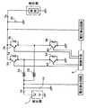
図1は、本発明の多相多重制御方式を実施するための電気回路構成図を示すもので低圧側の直流電源1の電圧をn倍に昇圧して高圧側の負荷10に供給する電圧にする機能と、逆に高圧側の電圧を1/nに降圧して低圧側に供給する機能を合わせ持っている。
図1において、直流電源1のプラス端子に接続された低圧側入出力端子Tlには2A、2B、…2XとN個のリアクトルが並列に接続されており、各リアクトルの他端には図のようにnpnトランジスタ3A、3B、…3Xと4A、4B、…4Xがブリッジ接続されている。そして、各トランジスタ3A、3B、…3Xと4A、4B、…4Xにはそれぞれダイオード7A、7B、…7Xと8A、8B、…8Xが並列に接続されている。
トランジスタ3A、3B、…3Xはエミッタが各リアクトル2A、2B、…2Xとそれぞれ接続されており、コレクタは高圧側入出力端子Thに接続されている。また、トランジスタ4A、4B、…4Xはコレクタが各リアクトル2A、2B、…2Xとそれぞれ接続されており、エミッタ側はグランドに接地されている。トランジスタ3A、3B、…3N及び4A、4B、…4Nのベース端子はそれぞれ制御手段5に接続されている。
【0013】
なお、nとNの関係は、nに最も近い整数をN’としてN’の整数倍をNとしている。例えば、n=2の場合はN=2、4、6、…となり、Nは2、4、6、…の中から本発明の多相多重制御方式の条件を考慮して任意の数を選定して本発明の多相多重制御方式を実施する回路を構成することとなる。
【0014】
低圧側入出力端子Tl側には平滑用コンデンサ10が、高圧側入出力端子Th側には平滑用コンデンサ20がそれぞれ接続されている。
また、低圧側電圧と高圧側電圧をそれぞれ検出して制御手段5にフイードバックするためにTl側には電圧検出回路6aが、Th側には電圧検出回路6bが接続されている。
制御手段5は、トランジスタ3A、3B、…3X及び4A、4B、…4Xを駆動するパルスを出力して各リアクトル2A、2B、…2Xに流れる電流を2π/Nずつ位相をずらして流すように制御する。
【0015】
上記の構成によれば、低圧側電圧を昇圧して高圧側に出力する場合の動作は次のようになる。
各トランジスタ4A、4B、…4Xが制御手段5からの駆動するパルスによって位相が2π/Nずれた状態で順次ONされる。各トランジスタ4A、4B、…4XがONのときには、各リアクトル2A、2B、…2Xのトランジスタ側は接地されることになるので、直流電源1から各リアクトル2A、2B、…2Xを通って順次電流が流れる。このとき各リアクトルには流れる電流の2乗とリアクトルのインダクタンスに比例するエネルギーが蓄えられる。
各トランジスタ4A、4B、…4XがONからOFFとなるとリアクトルに蓄えられたエネルギーに応じた電流がダイオード7A、7B、…7Xを通じて順次流れる。このとき高圧側の電圧は電圧検出回路6aによって監視されていて所定の設定電圧以上のときのみ各トランジスタ4A、4B、…4XをOFFとする構成としている。
【0016】
次に、高圧側電圧を降圧して低圧側に出力する場合の動作は次のようになる。
各トランジスタ3A、3B、…3Xが制御手段5からの駆動するパルスによって位相が2π/Nずれた状態で順次ONされる。各トランジスタ3A、3B、…3XがONすることにより高圧側からトランジスタ3A、3B、…3Xとリアクトル2A、2B、…2Xを通って直流電源1へと順次電流が流れる。
次に、トランジスタ3AがOFFとされるとリアクトル2Aから直流電源1、ダイオード8A、リアクトル2Aのループで電流が流れる降圧回路として動作する。トランジスタ3Aに引き続いて位相が2π/Nずれた状態で3B、3C、…3Xの順でOFFされて、リアクトル2B、直流電源1、ダイオード8B、リアクトル2Bのループ、リアクトル2C、直流電源1、ダイオード8C、リアクトル2Cのループの順で降圧回路として動作する。
【0017】
(実施例1)
以下に、本発明の実施例を図面を参照して説明する。図2は低圧側の電源電圧を昇圧比2倍で高圧側に出力し、高圧側の電圧を降圧比1/2倍で降圧して低圧側に供給する場合の電気回路構成図を示す。図1の電気回路構成図でn=N=2の場合である。
実施の形態で述べた如く昇圧時には、トランジスタ4A、4Bが位相がπ((2π/N)=(2π/2)=2)ずれた状態でスイッチングされる。このときの、スイッチング素子と流れる電流のタイミングと波形を図3に示す。
図3は、横軸は時間を表し、縦軸はトランジスタのON及びOFFの状態、あるいは電流量を表している。A相とはリアクトル2Aのルートであり、B相とはリアクトル2Bのルートである。
図3において、(a)、(b)はトランジスタ4A、4Bはπの位相差でON状態となっている。トランジスタ4AがON及びOFFのときリアクトル2Aに流れる電流の立上がりの勾配と立下がりの勾配は次のようになる。
リアクトルのインダクタンスをL、印可電圧をV、流れる電流をIとすると
V=L×I
の関係がある。図3のA相の場合、直流電源1の電圧をV0、リアクトル2AのインダクタンスをL、電流の勾配は流れる電流の時間微分値であるからΔI/Δtとすると
V0=L(ΔI/Δt)
よって、立上がりの勾配(ΔI/Δt)はV0/Lとなる。
一方、トランジスタ4AがOFFとなってリアクトル2Aから高圧側に電流が流れるときの勾配は、
2V0(高圧側電圧)−V0(低圧側電圧)=L(ΔI/Δt)
よって、立下がりの勾配(ΔI/Δt)もV0/Lとなる。
従って、(C)にに示すように立上がりの勾配と立下がりの勾配は同一の傾斜となる。その結果、A相入力電流とB相入力電流を合成したもの、すなわち、直流電源1からリアクトル側に流れる入力合成電流は(e)に示すようにリップルのないフラットなものとなる。
また、A相出力電流とB相出力電流及び出力合成電流は(f)、(g)、(h)に示されている。なお、出力合成電流は、図2の平滑コンデンサ20によって平滑される前の波形を示している。
【0018】
次に、実施例1の降圧時の入力電流及び出力電流の波形について説明する。
図4は、図2の電気回路構成図で高圧側の電圧を1/2倍に降圧して低圧側に供給する場合のタイミングチャートと電流の波形を表したものである。
図4の(a)、(b)に示すようにトランジスタ3Aと3Bは、πの位相差をもってON状態となるように制御手段5によってスイッチングされる。トランジスタ3AがON状態のとき、高圧側よりリアクトル2AへとA相入力電流が流れる。このときの入力電流の波形は(c)に示すように時間とともに増加する。そのときの勾配は昇圧動作の説明で述べたようにリアクトルに印加される電圧とリアクトルのインダクタンスLの関係から求められV0/Lとなる。
同様にB相の入力電流は、A相入力電流より位相がπずれた状態で(d)に示すように流れる。従って、入力合成電流は(e)に示すようになる。
次に、A相出力電流は、トランジスタ3AがONの期間は、V0/Lの勾配で増加し、トランジスタ3AがONからOFFとなると、ダイオード8A、リアクトル2A、直流電源1のループで流れる電流は減少していく。このときの勾配は直流電源1の電圧V0とリアクトルのインダクタンスLで定まりV0/Lである。
従って、A相出力電流は(f)に示す波形となる。同様にB相出力電流は(g)に示す波形となるので出力合成電流はフラットとなり、出力側(低圧側)のリップルの発生が押さえられる。
【0019】
(実施例2)
本発明に係わる実施例2は、N=4の場合で図1において、リアクトルが2A、2B、2C、2Dと、それぞれのリアクトルにブリッジ接続されるスイッチングトランジスタも3A、3B、3C、3D及び4A、4B、4C、4Dと各4組から構成され、昇圧比が4倍、降圧比が1/4倍の場合である。
なお、各トランジスタにはダイオード7A〜7D、8A〜8Dがそれぞれ並列に接続されている。
この回路構成の昇圧時の電流波形を図5に示す。図5には昇圧時の各相(A相、B相、C相、D相)のタイミングと電流波形が示されている。
例えば、A相の電流の立上がりの勾配は直流電源1の電圧をV0、リアクトルのインダクタンスをLとすると実施例1で述べたようにV0/Lとなる。立下がりの勾配は高圧側は4V0であるから
(4V0−V0)/L=3V0/L
となり、立下がりの勾配は立上がりの勾配の3倍の傾斜であることがわかる。B相、C相、D相も同様になる。
また、各相の位相のずれは2π/Nよりπ/2(N=4)となる。従って、A相、B相、C相、D相の入力電流は図5のようになり、その合成入力電流はフラットなリップルのないものとなる。
なお、図5は昇圧時の電流波形について述べられているが、降圧時も同様な波形なので低圧側の合成出力電流はリップルのないものが得られる。
【0020】
(実施例3)
実施例3は、請求項2の発明に係わるコンバータの多相多重制御方式で、電気自動車などで低圧側にバッテリを使用して高圧側ではインバータを介して電動発電機などを動作させる場合、バッテリの電圧変動に対して高圧側のインバータの電圧も可変として低圧側の電圧の整数倍(または整数に近い値)になるよう制御する方式である。
図6は、低圧側のバッテリの電圧が100〜300V間を変動するとしたとき高圧側(インバータ側)を500〜700V間で任意の電圧をとれるように制御する例を示している。
電気回路構成図としてはN=6とする。図6においてバッテリの電圧がP0〜P1にあるときは、昇降圧比が6倍となるように図1の制御手段5で制御する。このとき、インバータ側の電圧は600〜700Vの間で低圧側の電圧の6倍となるよう制御されている。
同様にバッテリの電圧がP2〜P3にあるときは昇降圧比が3倍となるように、バッテリの電圧がP4〜P5にあるときは昇降圧比が2倍となるように制御する。
この制御方式を行うことにより低圧側のバッテリの電圧が変動しても低圧側のリップルを最小限に抑えることが可能となる。
【0021】
(実施例4)
実施例4は、実施例3と同様に請求項2の発明に係わるコンバータの多相多重制御方式で、低圧側の電圧変動に対して高圧側のインバータの電圧を可変として昇降圧比を選択することで低圧側のリップルを抑えるものであるが、図7に示すように各リアクトルとスイッチングトランジスタの間にスイッチを設けることで相数を可変出来るようにしたものである。
図7は、図6の電圧条件に対応した電気回路でリアクトルは2A〜2Fと6個、スイッチもSW−A〜SW−Fと6個で構成されている。なお、図7では制御手段及び電圧検出回路は図示していない。
スイッチをON、OFF操作することにより相数を任意に設定するもので、例えば、スイッチSW−A〜SW−Eの5個をONとしてSW−FをOFFとすれば相数が5の回路となり、図6で昇降圧比5倍のものが実現できることになるので低圧側のリップルをさらに減少させる範囲を広げることが可能となる。
【0022】
【発明の効果】
以上述べたように、昇降圧比に基づいて相重数を選定すれば、特に低圧側のリップルを減少させることが出来て、他システムへの電源ノイズによる悪影響を防止する効果が大きい。また、平滑コンデンサの小型化など装置の小型化が可能となる。さらに、多相多重化により等価的に単相での高周波駆動を行うことに相当するため、各相単独では可聴域周波数での駆動であっても合成された結果、位相差による音圧相殺効果や可聴域外への高周波化が可能である。
【図面の簡単な説明】
【図1】本発明の電気回路構成図である。
【図2】本発明の実施例1の電気回路構成図である。
【図3】実施例1の昇圧時のタイミングチャートである。
【図4】実施例1の降圧時のタイミングチャートである。
【図5】実施例2の電流波形である。
【図6】実施例3の説明図である。
【図7】実施例4の電気回路構成図である。
【図8】従来例の電気回路構成図である。
【符号の説明】
1:直流電源
2A、2B、…2X:リアクトル
3A、3B、…3X:トランジスタ
4A、4B、…4X:トランジスタ
5:制御手段
6a、6b:電圧検出回路
7A、7B、…7X:ダイオード
8A、8B、…8X:ダイオード
10、20:平滑コンデンサ[0001]
TECHNICAL FIELD OF THE INVENTION
The present invention relates to a multi-phase multiplexed buck-boost converter having a function of obtaining a high-voltage output by boosting a low-voltage power supply by connecting a plurality of chopper devices in parallel, and a function of stepping down a high-voltage to a low-voltage side. Related to the control method.
[0002]
[Prior art]
2. Description of the Related Art Conventionally, as one of control methods of a switching type power supply device which boosts a low-voltage power supply to obtain a high-voltage output and operates a load connected to a high-voltage side, a plurality of chopper devices are connected in parallel and flow to each chopper device. A multi-phase multiplex chopper-type control method of operating a load on the output side by dividing a current and supplying the current with a phase shifted is used.
For example,
The multi-phase multiplex chopper type power supply device shown in FIG. 3 obtains a high-voltage output by boosting a low-voltage DC power supply by n (integer) times, and provides
[0003]
Here, if the switching timing of the transistors 14a to 14n is switched by the control means 15 in a state where the phases are shifted by 2π / n, the current flowing through the
[0004]
Further,
In the control method of the multi-phase multiplex chopper device of
Then, a deviation between the average current calculated from the total value of the output currents of the m chopper devices and the output current of each chopper device is obtained, and the deviation value is input to a PID controller (proportional-integral-differential controller). An output of an adjustment signal for reducing the input current deviation to zero is output from a PID controller and fed back to each chopper device to balance the output current of each chopper device.
[0005]
[Patent Document 1]
JP-A-10-127050 [Patent Document 2]
Japanese Patent Application Laid-Open No. 9-215322
[Problems to be solved by the invention]
However, the switching power supply device of
In an inverter system such as an electric vehicle, the voltage of a battery power supply on the low voltage side is boosted to drive various electric circuit devices and used as a drive power supply for a motor generator. On the other hand, since the regenerative power is stepped down and used for charging the battery power, it is desirable to have both the step-up and step-down functions.
Further, the control circuit of the polyphase multiplex chopper device disclosed in
[0007]
Therefore, in the present invention, in a multi-phase multiplex type buck-boost converter having both a step-up and a step-down function as a converter function, an optimal buck-boost ratio based on a buck-boost ratio for the purpose of ripple reduction and miniaturization or reduction of electronic components is proposed. It is an object of the present invention to provide a method for selecting an appropriate weight.
Further, when the voltage of the low-voltage side battery power source fluctuates, a control method for variably controlling the high-side voltage to appropriately select the step-up / step-down ratio between the low-side voltage and the high-side voltage is used to reduce the ripple. The task is to provide.
[0008]
[Means for Solving the Problems]
In order to solve the above-mentioned problem, a multi-phase multiplex control system according to
[0009]
That is, in a chopper type step-up / step-down converter in which the step-up ratio is n times and the step-down ratio is 1 / n times, the current flowing in each phase is controlled by shifting the phase by 2π / N by 2π / N as N-phase N-fold. In particular, when n is an integer, the ripple of the input current flowing from the low-voltage side power supply to the converter can be reduced to zero at the time of boosting. When the voltage on the high voltage side is reduced to the voltage on the low voltage side, the ripple of the current output from the converter to the low voltage side can be reduced to zero.
Further, even when n is not an integer, the ripple on the low voltage side can be suppressed low by setting the number of phases to the integer multiple N of the integer N ′ closest to n and setting N phases N times.
[0010]
According to a second aspect of the present invention, in the chopper type buck-boost converter according to the first aspect, the low-voltage side is controlled by controlling the high-side voltage with respect to a voltage fluctuation of the low-side DC power supply. It is characterized in that a ratio n between the side voltage and the high side voltage is selected.
[0011]
That is, in the buck-boost converter, when the voltage on the high voltage side is fixed and a battery or the like is used as the DC power supply on the low voltage side and the voltage fluctuates, the ratio n of the low voltage side voltage and the high voltage side fluctuates. Depending on the case, a large ripple may occur on the low pressure side.
Therefore, the voltage on the high voltage side is made variable within a certain range, and the voltage on the high voltage side is controlled with respect to the low voltage voltage so that n is positively set to be an integer (or a value close to an integer). The ripple on the low pressure side can be minimized.
[0012]
BEST MODE FOR CARRYING OUT THE INVENTION
Hereinafter, embodiments of the present invention will be described with reference to the drawings.
FIG. 1 shows an electric circuit configuration diagram for implementing the polyphase multiplexing control method of the present invention. The voltage of the low-voltage side
In FIG. 1,
The
[0013]
Note that the relationship between n and N is such that an integer closest to n is N ′ and an integer multiple of N ′ is N. For example, when n = 2, N = 2, 4, 6,..., And N is an arbitrary number selected from 2, 4, 6,... In consideration of the condition of the polyphase multiplex control system of the present invention. Thus, a circuit for implementing the multi-phase multiplex control method of the present invention is configured.
[0014]
A smoothing
A voltage detection circuit 6a is connected to the Tl side and a voltage detection circuit 6b is connected to the Th side in order to detect the low voltage side voltage and the high voltage side voltage, respectively, and feed them back to the control means 5.
The control means 5 outputs pulses for driving the
[0015]
According to the above configuration, the operation when the low voltage side voltage is boosted and output to the high voltage side is as follows.
The
When each of the
[0016]
Next, the operation when the high voltage side is stepped down and output to the low voltage side is as follows.
The
Next, when the transistor 3A is turned off, it operates as a step-down circuit in which a current flows from the
[0017]
(Example 1)
Hereinafter, embodiments of the present invention will be described with reference to the drawings. FIG. 2 shows an electric circuit configuration diagram in a case where the power supply voltage on the low voltage side is output to the high voltage side at a step-up ratio of twice, and the voltage on the high voltage side is stepped down at a step-down ratio of 1/2 and supplied to the low voltage side. This is the case where n = N = 2 in the electric circuit configuration diagram of FIG.
As described in the embodiment, at the time of boosting, the
In FIG. 3, the horizontal axis represents time, and the vertical axis represents the ON / OFF state of the transistor or the amount of current. The A phase is a route of the
In FIGS. 3A and 3B, in FIGS. 3A and 3B, the
When the inductance of the reactor is L, the applied voltage is V, and the flowing current is I, V = L × I
There is a relationship. In the case of the phase A in FIG. 3, the voltage of the
Therefore, the rising gradient (ΔI / Δt) is V0 / L.
On the other hand, when the
2V0 (high voltage) −V0 (low voltage) = L (ΔI / Δt)
Therefore, the falling slope (ΔI / Δt) is also V0 / L.
Accordingly, the rising slope and the falling slope have the same slope as shown in FIG. As a result, the combined A-phase input current and B-phase input current, that is, the combined input current flowing from the
The A-phase output current, the B-phase output current, and the output combined current are shown in (f), (g), and (h). The output combined current shows a waveform before being smoothed by the smoothing
[0018]
Next, waveforms of the input current and the output current at the time of step-down in the first embodiment will be described.
FIG. 4 shows a timing chart and a waveform of a current when the voltage on the high voltage side is reduced by half and supplied to the low voltage side in the electric circuit configuration diagram of FIG.
As shown in FIGS. 4A and 4B, the control means 5 switches the
Similarly, the B-phase input current flows as shown in (d) with the phase shifted by π from the A-phase input current. Therefore, the input combined current is as shown in FIG.
Next, the A-phase output current increases with a gradient of V0 / L while the transistor 3A is ON, and when the transistor 3A changes from ON to OFF, the current flowing through the loop of the
Therefore, the A-phase output current has a waveform shown in (f). Similarly, the B-phase output current has the waveform shown in (g), so that the output combined current becomes flat, and the generation of ripple on the output side (low voltage side) is suppressed.
[0019]
(Example 2)
Note that
FIG. 5 shows a current waveform at the time of boosting of this circuit configuration. FIG. 5 shows the timing and current waveform of each phase (A phase, B phase, C phase, and D phase) at the time of boosting.
For example, assuming that the voltage of the
It can be seen that the falling slope is three times the rising slope. The same applies to the B phase, C phase, and D phase.
Further, the phase shift of each phase becomes π / 2 (N = 4) from 2π / N. Therefore, the input currents of the A-phase, B-phase, C-phase, and D-phase are as shown in FIG. 5, and the combined input current has no flat ripple.
Although FIG. 5 describes the current waveform at the time of boosting, the waveform is the same at the time of step-down, so that the combined output current on the low voltage side has no ripple.
[0020]
(Example 3)
The third embodiment relates to a multi-phase multiplex control method of a converter according to the second aspect of the present invention. In a case where a battery is used on the low voltage side in an electric vehicle or the like and a motor generator or the like is operated via an inverter on the high voltage side, the battery is used. In this method, the voltage of the inverter on the high voltage side is also made variable with respect to the voltage fluctuation of (1), and is controlled to be an integral multiple (or a value close to an integer) of the voltage on the low voltage side.
FIG. 6 shows an example in which the high-voltage side (inverter side) is controlled to take an arbitrary voltage between 500 and 700 V when the voltage of the low-voltage side battery varies between 100 and 300 V.
It is assumed that N = 6 in the electric circuit configuration diagram. When the voltage of the battery is in the P0 to P1 in FIG. 6 is controlled by the
Similarly as in the buck-boost ratio when the voltage of the battery is in the P2 to P3 is 3-fold, when the voltage of the battery is in the P4 to P5 is controlled so as buck-boost ratio is doubled.
By performing this control method, it is possible to minimize the ripple on the low voltage side even if the voltage of the battery on the low voltage side fluctuates.
[0021]
(Example 4)
The fourth embodiment is a multi-phase multiplex control method of the converter according to the second aspect of the present invention, as in the third embodiment, wherein the step-up / step-down ratio is selected by making the voltage of the high-voltage inverter variable with respect to the low-voltage voltage fluctuation. In order to reduce the ripple on the low voltage side, the number of phases can be varied by providing a switch between each reactor and the switching transistor as shown in FIG.
FIG. 7 is an electric circuit corresponding to the voltage condition of FIG. 6 and includes six
The number of phases is arbitrarily set by operating the switches ON and OFF. For example, if five switches SW-A to SW-E are turned ON and SW-F is turned OFF, a circuit having five phases is obtained. 6, a step-up / step-down ratio of 5 can be realized, so that the range in which the ripple on the low voltage side can be further reduced can be expanded.
[0022]
【The invention's effect】
As described above, if the phase weight is selected based on the step-up / step-down ratio, the ripple on the low voltage side can be particularly reduced, and the effect of preventing the adverse effect of power supply noise on other systems is great. Also, the size of the device can be reduced, such as the size of the smoothing capacitor. Furthermore, since it is equivalent to performing high-frequency driving in a single phase equivalently by multi-phase multiplexing, the sound pressure canceling effect due to the phase difference as a result of combining each phase alone even if driving in the audible frequency range And higher frequencies outside the audible range.
[Brief description of the drawings]
FIG. 1 is an electric circuit configuration diagram of the present invention.
FIG. 2 is an electric circuit configuration diagram of
FIG. 3 is a timing chart at the time of boosting according to the first embodiment.
FIG. 4 is a timing chart at the time of step-down in the first embodiment.
FIG. 5 is a current waveform according to the second embodiment.
FIG. 6 is an explanatory diagram of a third embodiment.
FIG. 7 is an electric circuit configuration diagram of a fourth embodiment.
FIG. 8 is a configuration diagram of an electric circuit of a conventional example.
[Explanation of symbols]
1:
Claims (2)
Translated fromJapanesePriority Applications (1)
| Application Number | Priority Date | Filing Date | Title |
|---|---|---|---|
| JP2003151069AJP4110470B2 (en) | 2003-05-28 | 2003-05-28 | Multiphase multiple control system |
Applications Claiming Priority (1)
| Application Number | Priority Date | Filing Date | Title |
|---|---|---|---|
| JP2003151069AJP4110470B2 (en) | 2003-05-28 | 2003-05-28 | Multiphase multiple control system |
Publications (2)
| Publication Number | Publication Date |
|---|---|
| JP2004357388Atrue JP2004357388A (en) | 2004-12-16 |
| JP4110470B2 JP4110470B2 (en) | 2008-07-02 |
Family
ID=34046696
Family Applications (1)
| Application Number | Title | Priority Date | Filing Date |
|---|---|---|---|
| JP2003151069AExpired - Fee RelatedJP4110470B2 (en) | 2003-05-28 | 2003-05-28 | Multiphase multiple control system |
Country Status (1)
| Country | Link |
|---|---|
| JP (1) | JP4110470B2 (en) |
Cited By (29)
| Publication number | Priority date | Publication date | Assignee | Title |
|---|---|---|---|---|
| JP2006034091A (en)* | 2004-07-13 | 2006-02-02 | Marvell World Trade Ltd | Closed loop digital control system for single dc/dc converter |
| JP2006271062A (en)* | 2005-03-23 | 2006-10-05 | Advantest Corp | Power supply circuit and testing device |
| WO2008044619A1 (en)* | 2006-10-12 | 2008-04-17 | Toyota Jidosha Kabushiki Kaisha | Converter control device |
| WO2008047617A1 (en)* | 2006-10-20 | 2008-04-24 | Toyota Jidosha Kabushiki Kaisha | Converter control device |
| WO2009027523A1 (en)* | 2007-08-31 | 2009-03-05 | Kostal Industrie Elektrik Gmbh | Multi-channel dc controller operating independently of output power in critical conduction mode |
| EP2073364A1 (en) | 2007-12-21 | 2009-06-24 | Honda Motor Co., Ltd. | DC/DC converter apparatus, vehicle, fuel cell system, method of driving DC/DC converter, and DC/DC converter |
| EP2080662A1 (en) | 2008-01-16 | 2009-07-22 | Honda Motor Co., Ltd. | Fuel cell vehicle and DC/DC converter apparatus |
| JP2009171776A (en)* | 2008-01-18 | 2009-07-30 | Honda Motor Co Ltd | Power converter |
| US7576521B2 (en) | 2006-03-16 | 2009-08-18 | Fujitsu Ten Limited | Switching regulator |
| JP2009296775A (en)* | 2008-06-04 | 2009-12-17 | Sumitomo Heavy Ind Ltd | Converter |
| JP2009296774A (en)* | 2008-06-04 | 2009-12-17 | Sumitomo Heavy Ind Ltd | Converter |
| DE112008000189T5 (en) | 2007-01-24 | 2009-12-24 | Toyota Jidosha Kabushiki Kaisha, Toyota-shi | A multi-phase voltage conversion device, vehicle, and control method for a multi-phase voltage conversion device |
| JP2010104167A (en)* | 2008-10-24 | 2010-05-06 | Honda Motor Co Ltd | Power supply apparatus and power supply system of fuel cell vehicle |
| WO2010089888A1 (en)* | 2009-02-09 | 2010-08-12 | トヨタ自動車株式会社 | Power source system |
| US7932685B2 (en) | 2008-03-12 | 2011-04-26 | Denso Corporation | Control apparatus for power conversion apparatus and power conversion system |
| DE112009001399T5 (en) | 2008-06-13 | 2011-05-05 | Toyota Jidosha Kabushiki Kaisha, Toyota-shi | Signal control device |
| US7969039B2 (en) | 2008-03-25 | 2011-06-28 | Honda Motor Co., Ltd. | Method of controlling fuel cell vehicle and method of controlling DC/DC converter apparatus |
| KR101064764B1 (en) | 2009-12-30 | 2011-09-14 | 두산중공업 주식회사 | Expandable, non-isolated soft switching multiphase DC-DC converter with boost ratio and power capacity ratio |
| JP2011229315A (en)* | 2010-04-21 | 2011-11-10 | Sumitomo Heavy Ind Ltd | Charge/discharge inspection device |
| JP2012029487A (en)* | 2010-07-26 | 2012-02-09 | Mitsubishi Electric Corp | Multiple-chopper device |
| JP2012075201A (en)* | 2010-09-27 | 2012-04-12 | Panasonic Corp | Power supply device, and luminaire using the same |
| JP2012210138A (en)* | 2011-03-11 | 2012-10-25 | Denso Corp | Voltage conversion circuit, and voltage conversion system having the same |
| JP2013070614A (en)* | 2008-09-01 | 2013-04-18 | Mitsubishi Electric Corp | Converter circuit, and motor drive control device, air conditioner, refrigerator and induction heating cooker having the same |
| JP2013240133A (en)* | 2012-05-11 | 2013-11-28 | Tokyo Univ Of Science | Polyphase power conversion circuit |
| US8866331B2 (en) | 2008-10-24 | 2014-10-21 | Honda Motor Co., Ltd. | Power supply device and power supply system for fuel cell vehicle |
| JP2017085696A (en)* | 2015-10-23 | 2017-05-18 | トヨタ自動車株式会社 | Electric vehicle |
| JP2017099080A (en)* | 2015-11-19 | 2017-06-01 | 富士電機株式会社 | Battery connection method |
| JP2017143656A (en)* | 2016-02-10 | 2017-08-17 | トヨタ自動車株式会社 | Power supply |
| JP6771700B1 (en)* | 2020-01-28 | 2020-10-21 | 三菱電機株式会社 | Power converter |
Families Citing this family (1)
| Publication number | Priority date | Publication date | Assignee | Title |
|---|---|---|---|---|
| JP4611368B2 (en)* | 2007-12-21 | 2011-01-12 | 本田技研工業株式会社 | DC / DC converter device, vehicle, fuel cell system, and driving method of DC / DC converter device |
- 2003
- 2003-05-28JPJP2003151069Apatent/JP4110470B2/ennot_activeExpired - Fee Related
Cited By (42)
| Publication number | Priority date | Publication date | Assignee | Title |
|---|---|---|---|---|
| JP2006034091A (en)* | 2004-07-13 | 2006-02-02 | Marvell World Trade Ltd | Closed loop digital control system for single dc/dc converter |
| JP2006271062A (en)* | 2005-03-23 | 2006-10-05 | Advantest Corp | Power supply circuit and testing device |
| US7576521B2 (en) | 2006-03-16 | 2009-08-18 | Fujitsu Ten Limited | Switching regulator |
| WO2008044619A1 (en)* | 2006-10-12 | 2008-04-17 | Toyota Jidosha Kabushiki Kaisha | Converter control device |
| JP2008099455A (en)* | 2006-10-12 | 2008-04-24 | Toyota Motor Corp | Converter control device |
| US7633783B2 (en) | 2006-10-12 | 2009-12-15 | Toyota Jidosha Kabushiki Kaisha | Converter control device |
| KR101000425B1 (en) | 2006-10-12 | 2010-12-13 | 도요타 지도샤(주) | Converter Control |
| KR101002222B1 (en) | 2006-10-20 | 2010-12-20 | 도요타 지도샤(주) | Converter Control |
| JP2008104320A (en)* | 2006-10-20 | 2008-05-01 | Toyota Motor Corp | Converter control device |
| WO2008047617A1 (en)* | 2006-10-20 | 2008-04-24 | Toyota Jidosha Kabushiki Kaisha | Converter control device |
| US8159850B2 (en) | 2006-10-20 | 2012-04-17 | Toyota Jidosha Kabushiki Kaisha | Converter control device |
| DE112008000189T5 (en) | 2007-01-24 | 2009-12-24 | Toyota Jidosha Kabushiki Kaisha, Toyota-shi | A multi-phase voltage conversion device, vehicle, and control method for a multi-phase voltage conversion device |
| US8050065B2 (en) | 2007-01-24 | 2011-11-01 | Toyota Jidosha Kabushiki Kaisha | Multi-phase voltage converting device, vehicle and control method of multi-phase voltage converting device |
| WO2009027523A1 (en)* | 2007-08-31 | 2009-03-05 | Kostal Industrie Elektrik Gmbh | Multi-channel dc controller operating independently of output power in critical conduction mode |
| EP2073364A1 (en) | 2007-12-21 | 2009-06-24 | Honda Motor Co., Ltd. | DC/DC converter apparatus, vehicle, fuel cell system, method of driving DC/DC converter, and DC/DC converter |
| US7843713B2 (en) | 2007-12-21 | 2010-11-30 | Honda Motor Co., Ltd. | Method of driving DC/DC converter, and DC/DC converter |
| EP2080662A1 (en) | 2008-01-16 | 2009-07-22 | Honda Motor Co., Ltd. | Fuel cell vehicle and DC/DC converter apparatus |
| EP2080662B1 (en)* | 2008-01-16 | 2013-02-27 | Honda Motor Co., Ltd. | Fuel cell vehicle and DC/DC converter apparatus |
| JP2009171776A (en)* | 2008-01-18 | 2009-07-30 | Honda Motor Co Ltd | Power converter |
| US7932685B2 (en) | 2008-03-12 | 2011-04-26 | Denso Corporation | Control apparatus for power conversion apparatus and power conversion system |
| US7969039B2 (en) | 2008-03-25 | 2011-06-28 | Honda Motor Co., Ltd. | Method of controlling fuel cell vehicle and method of controlling DC/DC converter apparatus |
| JP2009296774A (en)* | 2008-06-04 | 2009-12-17 | Sumitomo Heavy Ind Ltd | Converter |
| JP2009296775A (en)* | 2008-06-04 | 2009-12-17 | Sumitomo Heavy Ind Ltd | Converter |
| DE112009001399T5 (en) | 2008-06-13 | 2011-05-05 | Toyota Jidosha Kabushiki Kaisha, Toyota-shi | Signal control device |
| US8378729B2 (en) | 2008-06-13 | 2013-02-19 | Toyota Jidosha Kabushiki Kaisha | Signal control device |
| US8817506B2 (en) | 2008-09-01 | 2014-08-26 | Mitsubishi Electric Corporation | Converter circuit, and motor drive control apparatus, air-conditioner, refrigerator, and induction heating cooker provided with the circuit |
| JP2013070614A (en)* | 2008-09-01 | 2013-04-18 | Mitsubishi Electric Corp | Converter circuit, and motor drive control device, air conditioner, refrigerator and induction heating cooker having the same |
| US8866331B2 (en) | 2008-10-24 | 2014-10-21 | Honda Motor Co., Ltd. | Power supply device and power supply system for fuel cell vehicle |
| JP2010104167A (en)* | 2008-10-24 | 2010-05-06 | Honda Motor Co Ltd | Power supply apparatus and power supply system of fuel cell vehicle |
| WO2010089888A1 (en)* | 2009-02-09 | 2010-08-12 | トヨタ自動車株式会社 | Power source system |
| KR101064764B1 (en) | 2009-12-30 | 2011-09-14 | 두산중공업 주식회사 | Expandable, non-isolated soft switching multiphase DC-DC converter with boost ratio and power capacity ratio |
| JP2011229315A (en)* | 2010-04-21 | 2011-11-10 | Sumitomo Heavy Ind Ltd | Charge/discharge inspection device |
| JP2012029487A (en)* | 2010-07-26 | 2012-02-09 | Mitsubishi Electric Corp | Multiple-chopper device |
| JP2012075201A (en)* | 2010-09-27 | 2012-04-12 | Panasonic Corp | Power supply device, and luminaire using the same |
| JP2012210138A (en)* | 2011-03-11 | 2012-10-25 | Denso Corp | Voltage conversion circuit, and voltage conversion system having the same |
| US8884564B2 (en) | 2011-03-11 | 2014-11-11 | Denso Corporation | Voltage converter and voltage converter system including voltage converter |
| JP2013240133A (en)* | 2012-05-11 | 2013-11-28 | Tokyo Univ Of Science | Polyphase power conversion circuit |
| JP2017085696A (en)* | 2015-10-23 | 2017-05-18 | トヨタ自動車株式会社 | Electric vehicle |
| JP2017099080A (en)* | 2015-11-19 | 2017-06-01 | 富士電機株式会社 | Battery connection method |
| JP2017143656A (en)* | 2016-02-10 | 2017-08-17 | トヨタ自動車株式会社 | Power supply |
| JP6771700B1 (en)* | 2020-01-28 | 2020-10-21 | 三菱電機株式会社 | Power converter |
| WO2021152688A1 (en)* | 2020-01-28 | 2021-08-05 | 三菱電機株式会社 | Power conversion device |
Also Published As
| Publication number | Publication date |
|---|---|
| JP4110470B2 (en) | 2008-07-02 |
Similar Documents
| Publication | Publication Date | Title |
|---|---|---|
| JP4110470B2 (en) | Multiphase multiple control system | |
| US10892686B2 (en) | Hysteretic control for transformer based power converters | |
| US7372239B2 (en) | Multi-output type DC/DC converter | |
| JP4196867B2 (en) | Bidirectional buck-boost chopper circuit, inverter circuit using the same, and DC-DC converter circuit | |
| US7733070B2 (en) | Multi-output type DC/DC converter | |
| JP5660025B2 (en) | Voltage conversion circuit and voltage conversion system including the voltage conversion circuit | |
| US9093901B2 (en) | Switching converter and method for controlling a switching converter | |
| US8354829B2 (en) | Apparatus, method and system for control of AC/AC conversion | |
| JP4672363B2 (en) | Converter power circuit | |
| US9236804B2 (en) | Regulated controller with self-adjusting output set-point control | |
| US7035125B2 (en) | Switching power supply and control method for the same | |
| US20080089102A1 (en) | Power converter control and power conversion method | |
| US11165339B2 (en) | Method for operating a power converter | |
| WO2009008223A1 (en) | Multi-output power supply device | |
| CN105871208A (en) | Multi-phase switching voltage regulator having asymmetric phase inductance | |
| JP2000092856A (en) | Switching amplifier apparatus | |
| JP2015015785A (en) | Buck dc/dc converter, controller for and method of controlling the same, and electronic apparatus using the same | |
| JP2008199808A (en) | Grid-connected inverter device | |
| CN107342681B (en) | Method and apparatus for efficient switching in a semi-resonant power converter | |
| JP2013021790A (en) | Control circuit and control method for switching power supply, and test device using them | |
| CA2746490A1 (en) | Converter device and method for controlling a converter device | |
| JP4252269B2 (en) | Multi-output DC-DC converter | |
| JP2014239579A (en) | Dc/dc converter and battery charging/discharging device | |
| US7298197B2 (en) | Multi-phase DC-DC converter with shared control | |
| US11190101B2 (en) | System and method for balancing current of converter phases |
Legal Events
| Date | Code | Title | Description |
|---|---|---|---|
| A621 | Written request for application examination | Free format text:JAPANESE INTERMEDIATE CODE: A621 Effective date:20050714 | |
| A977 | Report on retrieval | Free format text:JAPANESE INTERMEDIATE CODE: A971007 Effective date:20070816 | |
| A131 | Notification of reasons for refusal | Free format text:JAPANESE INTERMEDIATE CODE: A131 Effective date:20070911 | |
| A521 | Written amendment | Free format text:JAPANESE INTERMEDIATE CODE: A523 Effective date:20071109 | |
| TRDD | Decision of grant or rejection written | ||
| A01 | Written decision to grant a patent or to grant a registration (utility model) | Free format text:JAPANESE INTERMEDIATE CODE: A01 Effective date:20080313 | |
| A61 | First payment of annual fees (during grant procedure) | Free format text:JAPANESE INTERMEDIATE CODE: A61 Effective date:20080326 | |
| R150 | Certificate of patent or registration of utility model | Free format text:JAPANESE INTERMEDIATE CODE: R150 | |
| FPAY | Renewal fee payment (event date is renewal date of database) | Free format text:PAYMENT UNTIL: 20110418 Year of fee payment:3 | |
| FPAY | Renewal fee payment (event date is renewal date of database) | Free format text:PAYMENT UNTIL: 20120418 Year of fee payment:4 | |
| FPAY | Renewal fee payment (event date is renewal date of database) | Free format text:PAYMENT UNTIL: 20120418 Year of fee payment:4 | |
| FPAY | Renewal fee payment (event date is renewal date of database) | Free format text:PAYMENT UNTIL: 20130418 Year of fee payment:5 | |
| FPAY | Renewal fee payment (event date is renewal date of database) | Free format text:PAYMENT UNTIL: 20130418 Year of fee payment:5 | |
| FPAY | Renewal fee payment (event date is renewal date of database) | Free format text:PAYMENT UNTIL: 20140418 Year of fee payment:6 | |
| R250 | Receipt of annual fees | Free format text:JAPANESE INTERMEDIATE CODE: R250 | |
| R250 | Receipt of annual fees | Free format text:JAPANESE INTERMEDIATE CODE: R250 | |
| R250 | Receipt of annual fees | Free format text:JAPANESE INTERMEDIATE CODE: R250 | |
| LAPS | Cancellation because of no payment of annual fees |