JP2004356614A - Semiconductor storage device - Google Patents
Semiconductor storage deviceDownload PDFInfo
- Publication number
- JP2004356614A JP2004356614AJP2003416835AJP2003416835AJP2004356614AJP 2004356614 AJP2004356614 AJP 2004356614AJP 2003416835 AJP2003416835 AJP 2003416835AJP 2003416835 AJP2003416835 AJP 2003416835AJP 2004356614 AJP2004356614 AJP 2004356614A
- Authority
- JP
- Japan
- Prior art keywords
- memory device
- semiconductor memory
- memory cell
- gate
- metal
- Prior art date
- Legal status (The legal status is an assumption and is not a legal conclusion. Google has not performed a legal analysis and makes no representation as to the accuracy of the status listed.)
- Withdrawn
Links
- 239000004065semiconductorSubstances0.000titleclaimsabstractdescription75
- 229910052751metalInorganic materials0.000claimsabstractdescription52
- 239000002184metalSubstances0.000claimsabstractdescription52
- 229910021420polycrystalline siliconInorganic materials0.000claimsabstractdescription43
- 229920005591polysiliconPolymers0.000claimsabstractdescription43
- 239000011229interlayerSubstances0.000claimsabstractdescription9
- WFKWXMTUELFFGS-UHFFFAOYSA-NtungstenChemical compound[W]WFKWXMTUELFFGS-UHFFFAOYSA-N0.000claimsabstractdescription4
- 239000010937tungstenSubstances0.000claimsabstractdescription4
- 229910052721tungstenInorganic materials0.000claimsabstractdescription4
- 239000010410layerSubstances0.000claimsdescription58
- 239000010408filmSubstances0.000claimsdescription47
- 239000000758substrateSubstances0.000claimsdescription19
- 230000004888barrier functionEffects0.000claimsdescription16
- 239000003990capacitorSubstances0.000claimsdescription16
- 239000010409thin filmSubstances0.000claimsdescription6
- 238000009792diffusion processMethods0.000claimsdescription3
- NRTOMJZYCJJWKI-UHFFFAOYSA-NTitanium nitrideChemical compound[Ti]#NNRTOMJZYCJJWKI-UHFFFAOYSA-N0.000claimsdescription2
- 239000010941cobaltSubstances0.000claimsdescription2
- 229910017052cobaltInorganic materials0.000claimsdescription2
- GUTLYIVDDKVIGB-UHFFFAOYSA-Ncobalt atomChemical compound[Co]GUTLYIVDDKVIGB-UHFFFAOYSA-N0.000claimsdescription2
- 239000007772electrode materialSubstances0.000claimsdescription2
- 229910021332silicideInorganic materials0.000claimsdescription2
- FVBUAEGBCNSCDD-UHFFFAOYSA-Nsilicide(4-)Chemical compound[Si-4]FVBUAEGBCNSCDD-UHFFFAOYSA-N0.000claimsdescription2
- 229910021334nickel silicideInorganic materials0.000claims1
- RUFLMLWJRZAWLJ-UHFFFAOYSA-Nnickel silicideChemical compound[Ni]=[Si]=[Ni]RUFLMLWJRZAWLJ-UHFFFAOYSA-N0.000claims1
- 229910021341titanium silicideInorganic materials0.000claims1
- 239000012535impuritySubstances0.000abstractdescription57
- 230000008018meltingEffects0.000abstractdescription8
- 238000002844meltingMethods0.000abstractdescription8
- 230000009467reductionEffects0.000abstractdescription4
- 230000010485copingEffects0.000abstract1
- 238000009413insulationMethods0.000abstract1
- 238000003475laminationMethods0.000abstract1
- 229910000676Si alloyInorganic materials0.000description23
- 239000012212insulatorSubstances0.000description23
- 239000000872bufferSubstances0.000description19
- 238000010586diagramMethods0.000description14
- 238000000034methodMethods0.000description9
- 230000004048modificationEffects0.000description8
- 238000012986modificationMethods0.000description8
- 229910045601alloyInorganic materials0.000description5
- 239000000956alloySubstances0.000description5
- 230000008859changeEffects0.000description4
- 230000015572biosynthetic processEffects0.000description3
- 230000000694effectsEffects0.000description3
- 238000005530etchingMethods0.000description3
- 230000006870functionEffects0.000description3
- 239000000463materialSubstances0.000description3
- 239000011159matrix materialSubstances0.000description3
- 230000008569processEffects0.000description3
- 230000004044responseEffects0.000description3
- 230000003068static effectEffects0.000description3
- 230000000295complement effectEffects0.000description2
- 239000000126substanceSubstances0.000description2
- XUIMIQQOPSSXEZ-UHFFFAOYSA-NSiliconChemical compound[Si]XUIMIQQOPSSXEZ-UHFFFAOYSA-N0.000description1
- UGACIEPFGXRWCH-UHFFFAOYSA-N[Si].[Ti]Chemical compound[Si].[Ti]UGACIEPFGXRWCH-UHFFFAOYSA-N0.000description1
- 238000005229chemical vapour depositionMethods0.000description1
- 238000009434installationMethods0.000description1
- 238000010030laminatingMethods0.000description1
- 238000004518low pressure chemical vapour depositionMethods0.000description1
- PEUPIGGLJVUNEU-UHFFFAOYSA-Nnickel siliconChemical compound[Si].[Ni]PEUPIGGLJVUNEU-UHFFFAOYSA-N0.000description1
- 238000005498polishingMethods0.000description1
- 238000007517polishing processMethods0.000description1
- 238000010248power generationMethods0.000description1
- 229910052710siliconInorganic materials0.000description1
- 239000010703siliconSubstances0.000description1
- WNUPENMBHHEARK-UHFFFAOYSA-Nsilicon tungstenChemical compound[Si].[W]WNUPENMBHHEARK-UHFFFAOYSA-N0.000description1
Images


Classifications
- G—PHYSICS
- G11—INFORMATION STORAGE
- G11C—STATIC STORES
- G11C11/00—Digital stores characterised by the use of particular electric or magnetic storage elements; Storage elements therefor
- G11C11/21—Digital stores characterised by the use of particular electric or magnetic storage elements; Storage elements therefor using electric elements
- G11C11/34—Digital stores characterised by the use of particular electric or magnetic storage elements; Storage elements therefor using electric elements using semiconductor devices
- G11C11/40—Digital stores characterised by the use of particular electric or magnetic storage elements; Storage elements therefor using electric elements using semiconductor devices using transistors
- G11C11/41—Digital stores characterised by the use of particular electric or magnetic storage elements; Storage elements therefor using electric elements using semiconductor devices using transistors forming static cells with positive feedback, i.e. cells not needing refreshing or charge regeneration, e.g. bistable multivibrator or Schmitt trigger
- G11C11/412—Digital stores characterised by the use of particular electric or magnetic storage elements; Storage elements therefor using electric elements using semiconductor devices using transistors forming static cells with positive feedback, i.e. cells not needing refreshing or charge regeneration, e.g. bistable multivibrator or Schmitt trigger using field-effect transistors only
- H—ELECTRICITY
- H10—SEMICONDUCTOR DEVICES; ELECTRIC SOLID-STATE DEVICES NOT OTHERWISE PROVIDED FOR
- H10B—ELECTRONIC MEMORY DEVICES
- H10B10/00—Static random access memory [SRAM] devices
- H—ELECTRICITY
- H10—SEMICONDUCTOR DEVICES; ELECTRIC SOLID-STATE DEVICES NOT OTHERWISE PROVIDED FOR
- H10B—ELECTRONIC MEMORY DEVICES
- H10B10/00—Static random access memory [SRAM] devices
- H10B10/12—Static random access memory [SRAM] devices comprising a MOSFET load element
- H—ELECTRICITY
- H10—SEMICONDUCTOR DEVICES; ELECTRIC SOLID-STATE DEVICES NOT OTHERWISE PROVIDED FOR
- H10B—ELECTRONIC MEMORY DEVICES
- H10B10/00—Static random access memory [SRAM] devices
- H10B10/15—Static random access memory [SRAM] devices comprising a resistor load element
- Y—GENERAL TAGGING OF NEW TECHNOLOGICAL DEVELOPMENTS; GENERAL TAGGING OF CROSS-SECTIONAL TECHNOLOGIES SPANNING OVER SEVERAL SECTIONS OF THE IPC; TECHNICAL SUBJECTS COVERED BY FORMER USPC CROSS-REFERENCE ART COLLECTIONS [XRACs] AND DIGESTS
- Y10—TECHNICAL SUBJECTS COVERED BY FORMER USPC
- Y10S—TECHNICAL SUBJECTS COVERED BY FORMER USPC CROSS-REFERENCE ART COLLECTIONS [XRACs] AND DIGESTS
- Y10S257/00—Active solid-state devices, e.g. transistors, solid-state diodes
- Y10S257/903—FET configuration adapted for use as static memory cell
- Y10S257/904—FET configuration adapted for use as static memory cell with passive components,, e.g. polysilicon resistors
Landscapes
- Engineering & Computer Science (AREA)
- Microelectronics & Electronic Packaging (AREA)
- Computer Hardware Design (AREA)
- Semiconductor Memories (AREA)
Abstract
Description
Translated fromJapaneseこの発明は、半導体記憶装置に関し、特に、スタティック型のメモリセルを備える半導体記憶装置に関する。 The present invention relates to a semiconductor memory device, and more particularly, to a semiconductor memory device including a static memory cell.
代表的な半導体記憶装置の1つであるSRAM(Static Random Access Memory)は、記憶データを保持するためのリフレッシュ動作が不要なRAMである。SRAMのメモリセルは、負荷素子およびドライバトランジスタからなる2つのインバータが交差接続されたフリップフロップがアクセストランジスタを介してビット線対に接続される構成となっている。 An SRAM (Static Random Access Memory), which is one of the typical semiconductor storage devices, is a RAM that does not require a refresh operation for holding stored data. The SRAM memory cell has a configuration in which a flip-flop in which two inverters each including a load element and a driver transistor are cross-connected is connected to a bit line pair via an access transistor.
SRAMにおける代表的なメモリセルとしては、負荷素子がPチャネルMOSトランジスタで構成され、ドライバトランジスタおよびアクセストランジスタがNチャネルMOSトランジスタで構成されるCMOS型メモリセルが一般的に知られている。このCMOS型メモリセルは、消費電力が小さく、また、CMOSの特性上、スタティックノイズマージン(Static Noise Margin、以下「SNM」とも称する。)特性に優れ、さらにソフトエラー耐性にも優れるという特性を有する。 As a typical memory cell in the SRAM, a CMOS memory cell in which a load element is configured by a P-channel MOS transistor and a driver transistor and an access transistor are configured by an N-channel MOS transistor is generally known. This CMOS type memory cell has characteristics of low power consumption, excellent static noise margin (hereinafter also referred to as “SNM”) characteristics, and excellent soft error resistance due to CMOS characteristics. .
SRAMにおけるその他の代表的なメモリセルとして、ポリシリコンからなる高抵抗素子で負荷素子が構成される高抵抗負荷型メモリセルや、ポリシリコンからなるPチャネル薄膜トランジスタ(以下、「PチャネルTFT(Thin Film Transistor)」とも称する。)で負荷素子が構成されるPチャネルTFT負荷型メモリセルも知られている。この高抵抗負荷型メモリセルおよびPチャネルTFT負荷型メモリセルは、1メモリセルあたりのバルクトランジスタの数が4つであるため、6つのバルクトランジスタで構成されるCMOS型メモリセルに比べてセル面積を小さくできるという利点を有する。 Other typical memory cells in an SRAM include a high resistance load type memory cell in which a load element is formed by a high resistance element made of polysilicon, a P-channel thin film transistor made of polysilicon (hereinafter, referred to as a “P-channel TFT (Thin Film TFT)”). Transistor) is also known as a P-channel TFT load type memory cell in which a load element is formed. Since the number of bulk transistors per memory cell of the high resistance load type memory cell and the P-channel TFT load type memory cell is four, the cell area is larger than that of the CMOS type memory cell composed of six bulk transistors. Can be reduced.
なお、ここで「バルクトランジスタ」とは、ポリシリコンからなる抵抗素子やPチャネルTFTのように基板上に形成される薄膜素子に対して、シリコン基板中に作り込まれるトランジスタを示している。 Here, the "bulk transistor" indicates a transistor formed in a silicon substrate with respect to a thin film element formed on the substrate, such as a resistance element made of polysilicon or a P-channel TFT.
また、低電圧化に対応するSRAMとして、特開平7−57476号公報には、アクセストランジスタがPチャネルMOSトランジスタで構成されたSRAMが開示されている。これにより、アクセストランジスタのゲート−ソース間電圧を電源電圧と等しくできるため、低電圧化によるセル電流の低下を防止することができ、低電圧下における動作が保証される(特許文献1参照)。
近年、電子機器の携帯化や省エネルギー化を背景に、半導体記憶装置に対する低消費電力化および小型化のニーズがますます高まってきている。消費電力は電源電圧の2乗に比例するため、低消費電力化に対しては、電源電圧の低電圧化が有効である。このことから、半導体記憶装置においては、低電圧下においても動作可能であって、かつ、高いパフォーマンスを有する半導体記憶装置を提供することが従来より課題とされている。 2. Description of the Related Art In recent years, with the background of portable electronic devices and energy saving, there is an increasing need for low power consumption and miniaturization of semiconductor memory devices. Since power consumption is proportional to the square of the power supply voltage, lowering the power supply voltage is effective in reducing power consumption. For this reason, it has conventionally been an issue to provide a semiconductor memory device that can operate even at a low voltage and has high performance.
ここで、「低電圧」とは、3V未満を示すことが一般的であり、近年は、従来よく用いられていた3.3Vから2.5V、1.8Vへと電源電圧が低電圧化する傾向にある。 Here, the “low voltage” generally indicates less than 3 V. In recent years, the power supply voltage has been reduced from 3.3 V, which has been conventionally used, to 2.5 V and 1.8 V. There is a tendency.
上記課題に対して、低電圧下で使用されるSRAMにおいては、上述したCMOS型メモリセルが従来より採用されている。その理由は、上述した従来の高抵抗負荷型メモリセルやPチャネルTFT負荷型メモリセルでは、これらの負荷素子の電流駆動能力が小さいためにSNMが小さく、低電圧下での動作が不安定になるところ、CMOS型メモリセルは、CMOSの特性上SNMが大きく、低電圧下においてもCMOSインバータが安定動作するからである。このため、現在の低電圧化の傾向においては、上述した従来の高抵抗負荷型メモリセルやPチャネルTFT負荷型メモリセルが採用されることはほとんどなく、CMOS型メモリセルが主流となっている。 In order to solve the above problem, in the SRAM used under a low voltage, the above-mentioned CMOS memory cell has been conventionally employed. The reason is that in the above-described conventional high-resistance load type memory cell and P-channel TFT load type memory cell, since the current driving capability of these load elements is small, the SNM is small, and the operation under low voltage becomes unstable. This is because the CMOS type memory cell has a large SNM due to CMOS characteristics, and the CMOS inverter operates stably even at a low voltage. For this reason, in the current trend of lowering the voltage, the above-described conventional high-resistance load type memory cells and P-channel TFT load type memory cells are rarely adopted, and CMOS type memory cells are mainly used. .
しかしながら、低電圧化が進むと、上述した従来のCMOS型メモリセルでも対応できなくなる。すなわち、このCMOS型メモリセルでは、NチャネルMOSトランジスタで構成されるアクセストランジスタのしきい値電圧によって、低電位である電源電位よりも記憶ノードの電位がさらに低下し、もはやドライバトランジスタをオンさせることができなくなるからである。 However, as the voltage is reduced, even the above-mentioned conventional CMOS memory cell cannot be used. In other words, in this CMOS type memory cell, the potential of the storage node is further reduced by the threshold voltage of the access transistor formed of the N-channel MOS transistor from the lower potential of the power supply potential, and the driver transistor is no longer turned on. Is no longer possible.
ここで、NチャネルMOSトランジスタのしきい値電圧を下げることも考えられるが、しきい値電圧の低下は、リーク電流の増加を招き、消費電力を逆に増加させてしまう。 Here, it is conceivable to lower the threshold voltage of the N-channel MOS transistor. However, the lowering of the threshold voltage causes an increase in leakage current and conversely increases power consumption.
そこで、上述した特開平7−57476号公報に記載されたSRAMは、記憶ノードの電位低下を招かないため、このような課題を解決するものとして有用であるといえるが、上述したように、近年は、低電力化に加え、電子機器の携帯化に伴なう小型化をさらに実現する半導体記憶装置の実現が望まれている。 Therefore, the SRAM described in the above-mentioned Japanese Patent Application Laid-Open No. 7-57476 does not cause a decrease in the potential of the storage node, and can be said to be useful as a solution to such a problem. Therefore, there is a demand for a semiconductor memory device that further realizes miniaturization accompanying the portability of electronic devices in addition to lower power consumption.
さらに、半導体記憶装置の小型化は、メモリセルに蓄えられる電荷量の減少を招くため、半導体記憶装置の小型化に伴なうソフトエラーの発生を防止することも重要な課題である。 Furthermore, miniaturization of a semiconductor memory device causes a reduction in the amount of electric charge stored in a memory cell. Therefore, it is also an important issue to prevent the occurrence of a soft error accompanying the miniaturization of a semiconductor memory device.
そこで、この発明は、かかる課題を解決するためになされたものであり、その目的は、低電力化に対応でき、かつ、小型化を実現する半導体記憶装置を提供することである。 Therefore, the present invention has been made to solve such a problem, and an object of the present invention is to provide a semiconductor memory device which can cope with low power consumption and realizes downsizing.
また、この発明の別の目的は、低電力化に対応でき、かつ、小型化を実現し、さらに、ソフトエラーの発生を防止して安定的に動作する半導体記憶装置を提供することである。 Another object of the present invention is to provide a semiconductor memory device which can cope with low power consumption, realizes miniaturization, and operates stably by preventing occurrence of soft errors.
この発明によれば、半導体記憶装置は、データを記憶するメモリセルと、メモリセルに接続されるワード線およびビット線対とを備え、メモリセルは、第1の負荷素子、およびNチャネルMOSトランジスタからなる第1の駆動素子で構成される第1のインバータと、第1のインバータと交差接続され、第2の負荷素子、およびNチャネルMOSトランジスタからなる第2の駆動素子で構成される第2のインバータと、第1および第2のインバータの出力ノードにそれぞれ接続される第1および第2の記憶ノードと、ワード線にゲート電極が接続されるPチャネルMOSトランジスタで各々が構成され、第1および第2の記憶ノードをビット線対の一方および他方のビット線にそれぞれ接続する第1および第2のゲート素子とを含み、第1の記憶ノードを構成する第1の金属配線は、基板表面に形成される第1の駆動素子および第1のゲート素子に積層して設けられ、第2の記憶ノードを構成する第2の金属配線は、基板表面に形成される第2の駆動素子および第2のゲート素子に積層して設けられ、第1および第2の負荷素子は、第1および第2の金属配線の上部に設けられる。 According to the present invention, a semiconductor memory device includes a memory cell for storing data, a word line and a bit line pair connected to the memory cell, and the memory cell includes a first load element and an N-channel MOS transistor. And a second drive element cross-connected to the first inverter and including a second load element and a second drive element including an N-channel MOS transistor. , First and second storage nodes respectively connected to output nodes of the first and second inverters, and P-channel MOS transistors each having a gate electrode connected to a word line. And first and second gate elements respectively connecting the second storage node to one and the other bit lines of the bit line pair. The first metal wiring forming the storage node is provided so as to be stacked on the first drive element and the first gate element formed on the substrate surface, and the second metal wiring forming the second storage node is And a second driving element and a second gate element formed on the surface of the substrate. The first and second load elements are provided above the first and second metal wirings.
この発明による半導体記憶装置によれば、メモリセルの構成において、PチャネルTFTまたはポリシリコンからなる高抵抗素子で負荷素子を構成し、かつ、アクセストランジスタをPチャネルMOSトランジスタで構成し、記憶ノードを構成する埋込配線および負荷素子をバルクトランジスタの上部に積層する構造としたので、低電圧化に対応でき、かつ、メモリセルを大幅に小型化することができる。 According to the semiconductor memory device of the present invention, in the configuration of a memory cell, a load element is formed by a high-resistance element made of a P-channel TFT or polysilicon, an access transistor is formed by a P-channel MOS transistor, and a storage node is formed. Since the embedded wiring and the load element are stacked on the bulk transistor, it is possible to cope with low voltage and to significantly reduce the size of the memory cell.
以下、本発明の実施の形態について、図面を参照しながら詳細に説明する。なお、図中同一または相当部分には同一符号を付してその説明は繰返さない。 Hereinafter, embodiments of the present invention will be described in detail with reference to the drawings. In the drawings, the same or corresponding portions have the same reference characters allotted, and description thereof will not be repeated.
実施の形態1.
図1は、この発明による半導体記憶装置の構成を概念的に示す全体ブロック図である。
FIG. 1 is an overall block diagram conceptually showing a configuration of a semiconductor memory device according to the present invention.
図1を参照して、半導体記憶装置10は、行アドレス端子12と、列アドレス端子14と、制御信号端子16と、データ入出力端子18と、電源端子20とを備える。また、半導体記憶装置10は、行アドレスバッファ22と、列アドレスバッファ24と、制御信号バッファ26と、入出力バッファ28とを備える。さらに、半導体記憶装置10は、行アドレスデコーダ30と、列アドレスデコーダ32と、センスアンプ/ライトドライバ34と、マルチプレクサ35と、メモリセルアレイ36と、内部電源発生回路38とを備える。 Referring to FIG. 1, a
行アドレス端子12および列アドレス端子14は、それぞれ行アドレス信号X0〜Xmおよび列アドレス信号Y0〜Yn(m,nは自然数)を受ける。制御信号端子16は、書込制御信号/W、出力許可信号/OEおよびチップセレクト信号/CSを受ける。
行アドレスバッファ22は、行アドレス信号X0〜Xmを取込み、内部行アドレス信号を発生して行アドレスデコーダ30へ出力する。列アドレスバッファ24は、列アドレス信号Y0〜Ynを取込み、内部列アドレス信号を発生して列アドレスデコーダ32へ出力する。制御信号バッファ26は、書込制御信号/W、出力許可信号/OE、およびチップセレクト信号/CSを取込み、書込許可信号WEおよび出力許可信号OEをセンスアンプ/ライトドライバ34へ出力する。
データ入出力端子18は、半導体記憶装置10において読み書きされるデータを外部とやり取りする端子であって、データ書込時は外部から入力されるデータDQ0〜DQi(iは自然数)を受け、データ読出時はデータDQ0〜DQiを外部へ出力する。 The data input /
入出力バッファ28は、データ書込時は、データDQ0〜DQiを取込んでラッチし、内部データIDQ0〜IDQiをセンスアンプ/ライトドライバ34へ出力する。一方、入出力バッファ28は、データ読出時は、センスアンプ/ライトドライバ34から受ける内部データIDQ0〜IDQiをデータ入出力端子18へ出力する。 When writing data, input /
電源端子20は、外部から外部電源電圧ext.Vccおよび設置電圧ext.Vssを受ける。内部電源発生回路38は、電源端子20から外部電源電圧ext.Vccおよび接地電圧ext.Vssを受けて所定の電位からなる電源電圧Vccを発生し、発生した電源電圧Vccを半導体記憶装置10の各内部回路へ出力する。そして、メモリセルアレイ36に含まれるメモリセルも、この電源電圧Vccに基づいて動作する。 The
この半導体記憶装置10においては、電源電圧Vccは1.8Vであり、電源電圧が低電圧化されている。しかしながら、後述するメモリセルの構成の説明で明らかになるように、この半導体記憶装置10においては、電源電圧Vccがこのような低電圧であっても、メモリセルを構成するトランジスタのしきい値電圧を下げることなく、メモリセルは安定して動作する。 In the
行アドレスデコーダ30は、行アドレス信号X0〜Xmに対応するメモリセルアレイ36上のワード線を選択する。行アドレスデコーダ30は、非選択のワード線に電源電圧Vccを印加し、選択されたワード線に接地電圧GNDを印加する。また、列アドレスデコーダ32は、列アドレス信号Y0〜Ynに対応するメモリセルアレイ36上のビット線対を選択するための列選択信号をマルチプレクサ35へ出力する。
センスアンプ/ライトドライバ34は、データ書込時は、制御信号バッファ26から書込許可信号WEを受け、入出力バッファ28から受ける内部データIDQ0〜IDQiの論理レベルに応じて、各内部データに対応するI/O線対のいずれか一方のI/O線に電源電圧Vccを印加し、他方のI/O線に接地電圧GNDを印加する。また、センスアンプ/ライトドライバ34は、データ読出時は、制御信号バッファ26から出力許可信号OEを受け、読出データに対応してI/O線対に発生する微小の電圧変化を検出/増幅し、読出データの論理レベルを判定して読出データを入出力バッファ28へ出力する。 At the time of data writing, sense amplifier /
マルチプレクサ35は、列アドレスデコーダ32から受ける列選択信号に応じて、対応するビット線対をI/O線対と接続する。
メモリセルアレイは36は、複数のメモリセルが行列状に配置された記憶素子群であり、各行にそれぞれ対応する複数のワード線を介して行アドレスデコーダ30と接続され、また、各列にそれぞれ対応する複数のビット線対を介してマルチプレクサ35と接続される。 The
この半導体記憶装置10においては、データ書込時は、行アドレス信号X0〜Xmに応じたワード線に行アドレスデコーダ30によって接地電圧GNDが印加され、列アドレス信号Y0〜Ynに応じたビット線対が列アドレスデコーダ30によって選択されてマルチプレクサ35によってI/O線対と接続される。そして、センスアンプ/ライトドライバ34は、入出力バッファ28から受ける内部データIDQ0〜IDQiをI/O線対に書込み、これによって、行アドレス信号X0〜Xmおよび列アドレス信号Y0〜Ynにより選択されたメモリセルに内部データIDQ0〜IDQiが書込まれる。 In data writing, in
一方、データ読出時は、各ビット線対が電源電位Vccにプリチャージされた後、列アドレス信号Y0〜Ynに応じたビット線対が列アドレスデコーダ30によって選択され、選択されたビット線対がマルチプレクサ35によってI/O線対と接続される。そして、行アドレス信号X0〜Xmに応じたワード線に行アドレスデコーダ30によって接地電位GNDが印加されると、選択されたメモリセルからビット線対およびI/O線対にデータが読出される。 On the other hand, at the time of data reading, after each bit line pair is precharged to power supply potential Vcc, a bit line pair corresponding to column address signals Y0 to Yn is selected by
そして、センスアンプ/ライトドライバ34は、読出データに対応してI/O線対に発生した微小の電圧変化を検出/増幅し、読出データを入出力バッファ28へ出力する。これによって、行アドレス信号X0〜Xmおよび列アドレス信号Y0〜Ynにより選択されたメモリセルから内部データIDQ0〜IDQiが読出される。 Then, the sense amplifier /
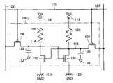
図2は、図1に示したメモリセルアレイ36上に行列状に配置されるメモリセルの構成を示す回路図である。 FIG. 2 is a circuit diagram showing a configuration of memory cells arranged in a matrix on
図2を参照して、メモリセル100は、NチャネルMOSトランジスタ102,104と、PチャネルMOSトランジスタ106,108と、PチャネルTFT110,112と、記憶ノード114,116とを備える。 Referring to FIG. 2,
PチャネルTFT110は、電源電圧Vccが印加される電源ノード118と記憶ノード114との間に接続され、ゲートが記憶ノード116に接続される。PチャネルTFT112は、電源ノード118と記憶ノード116との間に接続され、ゲートが記憶ノード114に接続される。 P-
PチャネルTFT110,112は、ポリシリコンからなるスイッチング機能を備えた抵抗素子であり、T(テラ、「T」は1012を表わす。)Ωオーダのオフ抵抗とG(ギガ、「G」は109を表わす。)Ωオーダのオン抵抗とを有する高抵抗素子である。 The P-
NチャネルMOSトランジスタ102は、記憶ノード114と接地電位GNDが印加される接地ノード120との間に接続され、ゲートが記憶ノード116に接続される。NチャネルMOSトランジスタ104は、記憶ノード116と接地ノード120との間に接続され、ゲートが記憶ノード114に接続される。 N-
NチャネルMOSトランジスタ102,104は、それぞれ記憶ノード114,116の電荷を引抜くドライバトランジスタである。なお、NチャネルMOSトランジスタ102,104は、それぞれ「第1の駆動素子」および「第2の駆動素子」を構成する。 N-
PチャネルTFT110およびNチャネルMOSトランジスタ102、ならびにPチャネルTFT112およびNチャネルMOSトランジスタ104は、それぞれインバータを構成し、この2つのインバータが交差接続されることによってフリップフロップが構成されている。これによって、記憶ノード114,116において相補なデータが双安定状態でラッチされ、メモリセル100にデータが記憶される。 P-
PチャネルMOSトランジスタ106は、ビット線122と記憶ノード114との間に接続され、ゲートがワード線126に接続される。PチャネルMOSトランジスタ108は、ビット線122に相補なビット線124と記憶ノード116との間に接続され、ゲートがワード線126に接続される。 P-
PチャネルMOSトランジスタ106,108は、ワード線126に接地電位GNDが印加されたときに、メモリセル100をそれぞれビット線対122,124に接続するアクセストランジスタである。なお、PチャネルMOSトランジスタ106,108は、それぞれ「第1のゲート素子」および「第2のゲート素子」を構成する。 P
次に、このメモリセル100の動作について説明する。 Next, the operation of the
(1)読出動作
メモリセル100にデータ“1”が書込まれている場合、すなわち、記憶ノード114,116の電位がそれぞれ“H(論理ハイ)レベル”,“L(論理ロー)レベル”に相当する電位の場合の読出動作について説明する。(1) Read Operation When data “1” is written in the
読出動作に先立って、ビット線122,124が電源電位Vccにプリチャージされる。その後、ワード線126が選択され、ワード線126に接地電位GNDが印加されると、アクセストランジスタであるPチャネルMOSトランジスタ106,108がオンする。そうすると、ビット線124からNチャネルMOSトランジスタ108を介して記憶ノード116に電荷が流れ込み、この流れ込んだ電荷は、NチャネルMOSトランジスタ104を介して放電される。これによって、ビット線124に電位変化が生じ、この変化を図示されないセンスアンプにより検出することによって、メモリセル100の記憶データ“1”が読出される。 Prior to the read operation,
ここで、このメモリセル100においては、負荷素子がPチャネルTFT110,112からなり、TFTは、電流駆動能力がバルクトランジスタに比べて大きく劣る。したがって、データ読出動作においては、負荷素子はほとんど機能せず、メモリセル100の動作特性は、アクセストランジスタおよびドライバトランジスタからなるCMOSインバータの特性が支配的になる。 Here, in the
図3は、図2に示したメモリセル100のデータ読出時におけるSNM特性図である。 FIG. 3 is an SNM characteristic diagram at the time of reading data from
図3を参照して、横軸および縦軸は、それぞれ記憶ノード114,116の電圧を示し、点S1,S2は、安定点を示す。曲線C1は、アクセストランジスタであるPチャネルMOSトランジスタ108およびドライバトランジスタであるNチャネルMOSトランジスタ104からなるインバータの伝達特性を示し、曲線C2は、アクセストランジスタであるPチャネルMOSトランジスタ106およびドライバトランジスタであるNチャネルMOSトランジスタ102からなるインバータの伝達特性を示す。 Referring to FIG. 3, the horizontal axis and the vertical axis indicate the voltages of
このメモリセル100は、アクセストランジスタがPチャネルMOSトランジスタで構成されるため、データ読出時は、アクセストランジスタおよびドライバトランジスタによってCMOSインバータが構成される。したがって、電源電圧Vccが低電圧であっても、図3に示すように、SNM(曲線C1,C2内部に形成される円の大きさがマージンを示す。)が十分に確保され、安定したデータ読出動作が実現される。 In
一方、図4は、アクセストランジスタをNチャネルMOSトランジスタで構成した場合のメモリセルのデータ読出時におけるSNM特性図である。 On the other hand, FIG. 4 is an SNM characteristic diagram at the time of reading data from a memory cell when the access transistor is formed of an N-channel MOS transistor.
図4を参照して、横軸および縦軸は、それぞれ記憶ノード114,116の電圧を示し、点S3,S4は、安定点を示す。曲線C3,C4は、アクセストランジスタおよびドライバトランジスタからなる各インバータの伝達特性を示す。このメモリセルにおいては、データ読出時は、アクセストランジスタおよびドライバトランジスタによってE−Eインバータが構成される。そして、データ読出時におけるこのメモリセルの動作特性は、このE−Eインバータによる動作特性が支配的になる。 Referring to FIG. 4, the horizontal axis and the vertical axis indicate the voltages of
したがって、図に示されるように、安定点S3,S4は、電源電圧VccからNチャネルMOSトランジスタのしきい値電圧Vthだけ低い値となり、特に、電源電圧Vccが低電圧になると、SNMマージンは極端に小さくなり、安定したデータ読出動作が実現できなくなる。 Therefore, as shown in the figure, the stable points S3 and S4 have a value lower than the power supply voltage Vcc by the threshold voltage Vth of the N-channel MOS transistor. In particular, when the power supply voltage Vcc is low, the SNM margin is extremely low. And a stable data read operation cannot be realized.
なお、上述した例では、メモリセル100にデータ“1”が記憶されている場合について説明したが、データ“0”が記憶されている場合についても同様に考えることができる。 In the above example, the case where data “1” is stored in the
(2)書込動作
再び図2を参照して、メモリセル100にデータ“0”を書込む場合、すなわち、記憶ノード114,116の電位をそれぞれ“Lレベル”,“Hレベル”に相当する電位にする場合について説明する。(2) Write Operation Referring to FIG. 2 again, when data "0" is written to
ワード線ドライバ(図示せず)によってワード線126に接地電圧GNDが印加され、PチャネルMOSトランジスタ106,108がオンした状態で、センスアンプ/ライトドライバ34(図示せず)によってビット線122,124にそれぞれ接地電圧GNDおよび電源電圧Vccが印加されると、ビット線124からPチャネルMOSトランジスタ108を介して記憶ノード116に電荷が供給される。一方、記憶ノード114からはNチャネルMOSトランジスタ106を介してビット線122に電荷が放電され、PチャネルTFT110,112およびNチャネルMOSトランジスタ102,104で構成されるフリップフロップの状態が設定される。 While the ground voltage GND is applied to the
なお、上述した例では、メモリセル100にデータ“0”を書込む場合について説明したが、データ“1”を書込む場合についても同様に考えることができる。 In the above example, the case where data “0” is written in the
次に、図2に示したメモリセル100の構造について説明する。負荷素子を構成するPチャネルTFT110,112は、バルクトランジスタであるNチャネルMOSトランジスタ102,104およびPチャネルMOSトランジスタ106,108の上部に形成される。これによって、このメモリセル100においては、低電圧化とともに小型化も同時に実現される。 Next, the structure of the
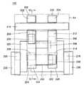
図5は、図2に示したメモリセル100の構造を示す平面図である。 FIG. 5 is a plan view showing the structure of the
図5を参照して、メモリセル100は、点線で示される不純物領域202〜216と、ゲート電極218と、L字型のゲート電極220,222と、埋込配線224〜230と、実線で示されるビット線コンタクト部232,234と、実線で示される接続開口部236,238と、一点鎖線で示されるTFTゲート部240,242とを含む。なお、後の断面図において説明するように、TFTゲート部240と埋込配線224との間にはTFTを構成するポリシリコン膜(ソース/ドレイン部)が形成されるが、図面による説明の関係上、その記載を省略している。 Referring to FIG. 5,
不純物領域202,210は、それぞれビット線コンタクト部232,234に接続される。不純物領域204,206は、埋込配線224に接続され、不純物領域212,214は、埋込配線226に接続される。また、不純物領域208,216は、それぞれ埋込配線228,230に接続される。
埋込配線224,226は、後述するように、ポリシリコン膜を形成する際の高温処理に耐えられる高融点の金属で構成される。そして、埋込配線224は、接続開口部236を介して図示されないPチャネルTFT110に接続され、さらに、PチャネルTFT112のゲートを構成するTFTゲート部242に接続される。また、埋込配線226は、接続開口部238を介して図示されないPチャネルTFT112に接続され、さらに、PチャネルTFT110のゲートを構成するTFTゲート部240に接続される。TFTゲート部240,242を含むPチャネルTFT110,112が形成される層の上部には、それぞれビット線コンタクト部232,234に接続される図示されないビット線122,124が形成されている。 The buried wirings 224 and 226 are made of a metal having a high melting point that can withstand high-temperature processing when forming a polysilicon film, as described later. The buried
なお、接続開口部236,238は、「第1の接続部」,「第2の接続部」を構成する。 The
埋込配線224およびゲート電極222の重なり部分である領域244は、埋込配線224およびゲート電極222が電気的に接続されている部分である。すなわち、ゲート電極は、絶縁体で周囲が覆われているところ、領域244においては、ゲート電極222の周囲の絶縁体が除去されており、埋込配線224がゲート電極222に直接接合されている。同様に、埋込配線226およびゲート電極220の重なり部分である領域246は、埋込配線226およびゲート電極220が電気的に接続されている部分である。 A
また、埋込配線224は、ゲート電極218,220とはゲート電極218,220の周囲に設けられる絶縁体によって絶縁されている。さらに、埋込配線226は、ゲート電極218,222とはゲート電極218,222の周囲に設けられる絶縁体によって絶縁されている。この埋込配線224,226は、それぞれ記憶ノード114,116を構成する。 Further, the embedded
不純物領域202,204,210,212は、半導体基板上に形成されるN型ウェル内に設けられるP型の不純物領域である。不純物領域202,204およびゲート電極218は、アクセストランジスタであるPチャネルMOSトランジスタ106を構成する。不純物領域210,212およびゲート電極218は、アクセストランジスタであるPチャネルMOSトランジスタ108を構成する。 The
不純物領域206,208,214,216は、半導体基板上に形成されるP型ウェル内に設けられるN型の不純物領域である。不純物領域206,208およびゲート電極220は、ドライバトランジスタであるNチャネルMOSトランジスタ102を構成する。不純物領域214,216およびゲート電極222は、ドライバトランジスタであるNチャネルMOSトランジスタ104を構成する。 The
なお、一点鎖線で示される領域A1は、このメモリセル100の面積を示している。 A region A1 indicated by a dashed line indicates the area of the
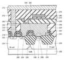
図6は、図5に示したメモリセル100の断面VI−VIの構造を示す断面図である。 FIG. 6 is a sectional view showing the structure of section VI-VI of
図6を参照して、半導体基板252上にN型ウェル254およびP型ウェル256が設けられる。N型ウェル254内には、不純物領域202,204が設けられ、P型ウェル256内には、不純物領域206が設けられる。フィールド酸化膜258,259は、N型ウェル254およびP型ウェル256上に形成される各素子を絶縁分離する。 Referring to FIG. 6, an N-
不純物領域202,204の間に形成されるチャネル形成領域の上部にゲート酸化膜260を介してゲート電極218が設けられる。また、フィールド酸化膜258,259の上部には、それぞれゲート電極220,222が設けられる。ゲート電極218〜222は、たとえば、高温プロセスに耐え得るポリシリコンや珪化タングステン(WSi)などからなる。 A
そして、ゲート電極218,220は、それぞれ絶縁体261,262で周囲が覆われ、ゲート電極222は、埋込配線224に接合される部分を除いて絶縁体264で周囲が覆われている。ここで、このゲート電極222が埋込配線224と接合されている部分が図5に示した領域244に相当する。 The periphery of the
記憶ノード114を構成する埋込配線224は、不純物領域204、絶縁体262で覆われたゲート電極220、不純物領域206、およびゲート電極222の上部に設けられる。より具体的には、絶縁体262,264よりも高くなる厚い膜厚からなる絶縁体266が各不純物領域および各ゲート電極の上部に堆積され、埋込配線224を形成するための溝が絶縁体266に設けられる。そして、この溝に導電性の金属が埋め込まれる。 The embedded
ここで、埋込配線224を構成する金属は、上述したゲート電極材よりも抵抗が低く、かつ、埋込配線224の上部に後述するポリシリコン膜270を形成する際に熱履歴を生じない高融点の金属からなる。 Here, the metal forming the embedded
埋込配線224に金属を用いるのは、極性の異なるトランジスタを電気的に接続するためである。また、埋込配線224に相当の厚さを設けるのは、埋込配線224における配線抵抗を低く抑え、電圧降下を抑制するためである。 The reason why metal is used for the embedded
また、埋込配線224に高融点の金属を用いるのは、以下の理由による。埋込配線224の上部には、層間絶縁膜268を介してポリシリコン膜270が形成される。ここで、ポリシリコン膜270の形成は、減圧CVD(Chemical Vapor Deposition)法によって行われることが一般的であり、このプロセスにおいては、たとえば600℃程度の高温処理がなされるところ、この処理温度に対して耐熱性を有する高融点の金属を埋込配線224に用いる必要がある。 The reason why the metal having a high melting point is used for the embedded
埋込配線224に用いる低抵抗かつ高融点の金属としては、たとえば、タングステンなどが好適である。 As a metal having a low resistance and a high melting point used for the buried
層間絶縁膜268を介して埋込配線224の上部に形成されたポリシリコン膜270は、接続開口部236を介して埋込配線224に接続される。そして、ポリシリコン膜270のさらに上部には、絶縁膜を介してTFTゲート部240が設けられ、ポリシリコン膜270およびTFTゲート部240によってPチャネルTFT110が構成される。 The
ポリシリコン膜270およびTFTゲート部240の上部には、層間絶縁膜274を介してビット線122を構成する金属配線276が設けられ、金属配線276は、ビット線コンタクト部272,232を介して不純物領域202と接続される。なお、埋込配線224およびビット線コンタクト部232と同層のその他の部分は、絶縁体266で構成される。 Above the
このように、このメモリセル100においては、ウェル上に形成されたバルクトランジスタの上部に記憶ノードを構成する埋込配線層を設け、さらにその上部に負荷素子であるPチャネルTFTを積層する構成としたので、メモリセル100の平面的な占有面積(図5に示した領域A1)は縮小される。 As described above, in the
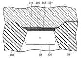
図7は、図6に示されるA部の拡大図である。 FIG. 7 is an enlarged view of a portion A shown in FIG.
図7を参照して、埋込配線224と不純物領域206とのコンタクト部には、第1のシリコン合金層278、第2のシリコン合金層280、およびバリアメタル層282が不純物領域206の上部に順に積層され、バリアメタル層282の上部に埋込配線224が設けられる。 Referring to FIG. 7, a first
第1のシリコン合金層278は、アロイスパイクによる接合不良を防止するために設けられる。ここで、アロイスパイクとは、不純物領域206に金属が侵入し、その侵入した金属がP型ウェル256にまで達することによって不純物領域206がP型ウェル256と短絡する現象であって、アロイスパイクの発生は、不純物領域206とP型ウェル256との接合不良を引き起こす。また、第1のシリコン合金層278は、上部に設けられる後述の第2のシリコン合金層280よりも耐熱性に優れ、不純物領域206中における拡散係数が第2のシリコン合金層280よりも小さいシリコン合金からなる。この第1のシリコン合金層278は、たとえば、珪化コバルト(CoSi)や珪化ニッケル(NiSi)などからなる。 The first
第2のシリコン合金層280は、埋込配線224と不純物領域206とのコンタクト部におけるオーミックコンタクトを形成するオーミックコンタクト材からなり、たとえば、珪化チタン(TiSi)などからなる。ここで、オーミックコンタクトとは、金属が半導体と接触する際の接触抵抗をデバイス性能に影響しないレベルまで低減させた接続のことをいう。 Second
バリアメタル層282は、埋込配線224の形成時に下層の第2のシリコン合金層280および/または第1のシリコン合金層278を保護するために設けられ、たとえば、窒化チタン(TiN)などからなる。
なお、上記において、第1のシリコン合金層278は、「第1の障壁層」を構成し、第2のシリコン合金層280は、「接続層」を構成し、バリアメタル層282は、「第2の障壁層」を構成する。 Note that, in the above description, the first
ここで、第2のシリコン合金層280の下部に第1のシリコン合金層278がさらに設けられるのは、以下の理由による。従来の高抵抗負荷型メモリセルやPチャネルTFT負荷型メモリセルにおいては、半導体基板中に形成される複数のバルクトランジスタは、いずれもN型であったため、これらのバルクトランジスタの接続に上記のような金属を用いる必要はなく、N型ポリシリコンなどによる接続が可能であった。 Here, the first
また、従来のCMOS型メモリセルにおいては、極性の異なるP型およびN形のバルクトランジスタが半導体基板中に形成されるため、これらの接続に金属が必要となる。しかしながら、CMOS型メモリセルにおいては、メモリセルを構成するトランジスタは、いずれも半導体基板中に形成されるので、高温処理されるポリシリコン層を上部に形成する必要はない。 Further, in a conventional CMOS memory cell, P-type and N-type bulk transistors having different polarities are formed in a semiconductor substrate, so that a metal is required for these connections. However, in the CMOS type memory cell, since all the transistors constituting the memory cell are formed in the semiconductor substrate, it is not necessary to form a polysilicon layer to be subjected to high temperature processing on the upper part.
一方、この実施の形態1においては、極性の異なるP型およびN形のバルクトランジスタが半導体基板中に形成され、これらを接続する金属(埋込配線224)が上部に形成され、さらにその上部に高温処理されるポリシリコン層270が形成される。したがって、この実施の形態1においては、アロイスパイクの発生を防止し、かつ、高温処理に対して耐熱性を有するコンタクト部の形成が要求されるところ、オーミックコンタクト材として機能する第2のシリコン合金層280と不純物領域206との間に、不純物領域206中における拡散係数が第2のシリコン合金層280よりも小さい、耐熱性に優れた第1のシリコン合金層278が設けられている。 On the other hand, in the first embodiment, P-type and N-type bulk transistors having different polarities are formed in a semiconductor substrate, and a metal (embedded wiring 224) connecting them is formed on the upper part, and further on the upper part. A
再び図6を参照して、絶縁体266およびそれに設けられる溝に金属を埋め込むことによって形成される埋込配線224の上面は、平坦加工される。具体的には、絶縁体266および埋込配線224の上面は、たとえばCMP(Chemical Mechanical Polishing:化学的機械的研磨)法やエッチングバック法によって、凹凸のない平面に加工される。ここで、CMP法とは、研磨剤の入った薬品を用いて砥石で対象面を研磨する方法である。また、エッチングバック法とは、レジスト膜の粘性を利用して表面を平坦化した後、上部から全面エッチングを行なう方法である。 Referring to FIG. 6 again, the upper surface of buried
ポリシリコン膜270の下地層、すなわち埋込配線224および絶縁体266からなる層の上面を平坦化するのは、ポリシリコン膜270によって構成されるPチャネルTFTの電気的特性が下地層表面の平坦性の影響を大きく受けるからである。そして、この平坦加工された面の上部に層間絶縁膜268を介してポリシリコン膜270が形成される。したがって、この実施の形態1によれば、PチャネルTFTの電気的特性が安定する。 The planarization of the underlayer of the
また、ポリシリコン膜270は、埋込配線224および絶縁体266からなる下地層に並行して設けられるので、ポリシリコン膜270によって構成されるPチャネルTFTの電気的特性を維持しつつ、ポリシリコン膜270を埋込配線224と接続するコンタクト部236のレイアウトパターンの自由度も向上する。 Also, since the
なお、特に図示しないが、図6における埋込配線224と不純物領域204とのコンタクト部、およびビット線コンタクト部232と不純物領域202とのコンタクト部においても、図7に示した埋込配線224と不純物領域206とのコンタクト部と同様に、第1のシリコン合金層278、第2のシリコン合金層280、およびバリアメタル層282が設けられる。 Although not particularly shown, the contact portions between the embedded
また、図5に示したもう1つの埋込配線226も、埋込配線224と同じ金属によって構成され、埋込配線226と不純物領域とのコンタクト部の構成、および埋込配線226の上面の平坦性についても、それぞれ図7および図6に示した構成と同じである。 Further, another buried
一方、図8は、アクセストランジスタがNチャネルMOSトランジスタで構成され、負荷素子がPチャネルMOSトランジスタで構成される場合のメモリセルの構造を示す平面図である。 On the other hand, FIG. 8 is a plan view showing the structure of a memory cell in the case where the access transistor is formed of an N-channel MOS transistor and the load element is formed of a P-channel MOS transistor.
図8を参照して、このメモリセルは、点線で示される不純物領域302〜317と、ゲート電極318と、T字型のゲート電極320と、L字型のゲート電極322と、埋込配線324〜330と、実線で示されるビット線コンタクト部332,334とを含む。これらの上部には、ビット線コンタクト部332,334に接続される図示されないビット線対が形成されている。 Referring to FIG. 8, this memory cell includes
不純物領域302,310は、それぞれビット線コンタクト部332,334に接続される。不純物領域304,306,307は、埋込配線324に接続され、不純物領域312,314,315は、埋込配線326に接続される。さらに、埋込配線328,330は、それぞれ不純物領域309,317に接続される。
埋込配線324およびゲート電極322の重なり部分である領域336は、埋込配線324およびゲート電極322が電気的に接続されている部分である。すなわち、ゲート電極は、絶縁体で周囲が覆われているところ、領域336においては、ゲート電極322の周囲の絶縁体が除去されており、埋込配線324がゲート電極322に直接接合されている。同様に、埋込配線326およびゲート電極320の重なり部分である領域338は、埋込配線326およびゲート電極320が電気的に接続されている部分である。 A
また、埋込配線324は、ゲート電極318,320とはゲート電極318,320の周囲に設けられる絶縁体によって絶縁されている。さらに、埋込配線326は、ゲート電極318,322とはゲート電極318,322の周囲に設けられる絶縁体によって絶縁されている。この埋込配線324,326は、このメモリセルにおける記憶ノードを構成する。 The embedded
不純物領域302〜306,308,310〜314,316は、半導体基板上に形成されるP型ウェル内に設けられるN型の不純物領域である。不純物領域302,304およびゲート電極318、ならびに不純物領域310,312およびゲート電極318は、それぞれアクセストランジスタであるNチャネルMOSトランジスタを構成する。また、不純物領域306,308およびゲート電極320、ならびに不純物領域314,316およびゲート電極322は、それぞれドライバトランジスタであるNチャネルMOSトランジスタを構成する。 The
不純物領域307,309,315,317は、半導体基板上に形成されるN型ウェル内に設けられるP型の不純物領域である。不純物領域307,309およびゲート電極320、ならびに不純物領域315,317およびゲート電極322は、それぞれ負荷素子であるPチャネルMOSトランジスタを構成する。 The
なお、一点鎖線で示される領域A2は、このメモリセルの面積を示している。 A region A2 indicated by a dashed line indicates the area of the memory cell.
図9は、図8に示したメモリセルの断面IX−IXの構造を示す断面図である。 FIG. 9 is a cross-sectional view showing a structure of a cross-section IX-IX of the memory cell shown in FIG.
図9を参照して、半導体基板352上にP型ウェル354およびN型ウェル356が設けられる。P型ウェル354内には、不純物領域302〜306が設けられ、N型ウェル356内には、不純物領域307が設けられる。フィールド酸化膜358〜360は、P型ウェル354およびN型ウェル356上に形成される各素子を絶縁分離する。 Referring to FIG. 9, a P-
不純物領域302,304の間に形成されるチャネル形成領域の上部にゲート酸化膜361を介してゲート電極318が設けられる。また、フィールド酸化膜359,360の上部には、それぞれゲート電極320,322が設けられる。ゲート電極318,320は、それぞれ絶縁体361,362で周囲が覆われ、ゲート電極322は、埋込配線324と接続される部分を除いて絶縁体364で周囲が覆われている。ここで、このゲート電極322が埋込配線324と接合されている部分が図8に示した領域336に相当する。 A
記憶ノードを構成する埋込配線324は、不純物領域304、フィールド酸化膜358、不純物領域306、絶縁体363で覆われたゲート電極320、不純物領域307、およびゲート電極322の上部に設けられる。そして、埋込配線324のさらに上部には、層間絶縁膜370を介してビット線を構成する金属配線372が設けられ、金属配線372は、ビット線コンタクト部368,332を介して不純物領域302と接続される。なお、埋込配線324およびビット線コンタクト部332と同層のその他の部分は、絶縁体366で構成される。 The embedded
再び図5および図8を参照して、両メモリセルの面積を示す領域A1,A2を比較すると、領域A1は、領域A2の約0.6倍である。すなわち、この発明におけるメモリセル100は、上述した積層構造によって、負荷素子がPチャネルMOSトランジスタで構成されるメモリセルに比べて、面積が約4割削減される。 Referring again to FIGS. 5 and 8, comparing regions A1 and A2 indicating the areas of both memory cells, region A1 is approximately 0.6 times as large as region A2. That is, the
実施の形態1の変形例.
図10は、図6に示したメモリセルの変形例を示す断面図である。Modification of the first embodiment.
FIG. 10 is a sectional view showing a modification of the memory cell shown in FIG.
図10を参照して、このメモリセルは、図6に示したメモリセル100の構成において、ポリシリコン膜270に代えてポリシリコン膜270Aを備え、接続開口部236に代えてもう1つの埋込配線284を備える。 Referring to FIG. 10, this memory cell has the same structure as
埋込配線284は、ポリシリコン膜270Aを埋込配線224と電気的に接続する。この埋込配線284も、埋込配線224と同様に、ポリシリコン膜270を形成する際の熱履歴に耐えられる高融点の金属からなり、たとえばタングステンなどからなる。 The buried
この実施の形態1の変形例においては、コンタクト部を構成するためにポリシリコン膜に窪みを設ける必要がない。したがって、ポリシリコン膜270Aをさらに精度よく均一化することができ、ポリシリコン膜270Aによって構成されるPチャネルTFTの電気的特性がさらに安定化する。 In the modification of the first embodiment, it is not necessary to provide a depression in the polysilicon film to form the contact portion. Therefore, the
以上のように、実施の形態1またはその変形例による半導体記憶装置10によれば、負荷素子およびアクセストランジスタをそれぞれPチャネルTFTおよびPチャネルMOSトランジスタで構成し、記憶ノードを構成する埋込配線および負荷素子を構成するPチャネルTFTをバルクトランジスタの上部に積層する構造としたので、低電圧化に対応でき、かつ、メモリセル100を大幅に小型化することができる。 As described above, according to the
また、この半導体記憶装置10によれば、記憶ノードを高融点の金属で埋込配線化したので、トランジスタ間の抵抗が低く抑えられ、電圧降下が抑制されるとともに、埋込配線においてその上部にポリシリコン膜を形成する際の高温処理による熱履歴を生じない。 Further, according to the
また、この半導体記憶装置10によれば、オーミックコンタクト材として機能する第2のシリコン合金層と不純物領域との間に耐熱性に優れる第1のシリコン合金層を設けたので、ポリシリコン膜を形成する際に高温処理がなされても、アロイスパイクの発生を防止することができる。 Further, according to the
また、この半導体記憶装置10によれば、ポリシリコン膜の下地層の上面を平坦化したので、そのポリシリコン膜によって構成されるPチャネルTFTの電気的特性が安定化され、さらに、ポリシリコン膜を埋込配線と接続するコンタクト部のレイアウトパターンの自由度が向上する。 Further, according to the
実施の形態2.
実施の形態2では、実施の形態1またはその変形例におけるメモリセルにおいて、記憶ノードにキャパシタが設けられる。これによって、記憶ノードの容量が増加し、ソフトエラー耐性が向上する。その結果、メモリセルの動作が安定する。
In the second embodiment, a capacitor is provided at a storage node in the memory cell according to the first embodiment or its modification. Thereby, the capacity of the storage node increases, and the soft error resistance improves. As a result, the operation of the memory cell is stabilized.
実施の形態2による半導体記憶装置の全体構成は、図1に示した半導体記憶装置10の構成と同じであるので、その説明は繰返さない。 The overall configuration of the semiconductor memory device according to the second embodiment is the same as that of
図11は、実施の形態2におけるメモリセルの構成を示す回路図である。 FIG. 11 is a circuit diagram showing a configuration of a memory cell according to the second embodiment.
図11を参照して、メモリセル100Aは、実施の形態1におけるメモリセル100の構成において、キャパシタ128,130と、定電位ノード132とをさらに備える。キャパシタ128は、記憶ノード114と定電位ノード132との間に接続される。キャパシタ130は、記憶ノード116と定電位ノード132との間に接続される。メモリセル100Aのその他の回路構成は、メモリセル100の構成と同じである。 Referring to FIG. 11,
このキャパシタ128,130は、基板の上部に積層して形成され、記憶ノード114,116を構成する埋込配線とコンタクトホールを介してそれぞれ接続される。これによって、記憶ノード114,116を構成する埋込配線の面積を増加させることなく、記憶ノード114,116の容量を増加させることができる。すなわち、キャパシタ128,130が設けられることによって、メモリセル100に比べて面積を増加させることなく、メモリセル100Aのソフトエラー耐性を向上させることができ、メモリセル100Aの動作を安定化することができる。 These
以上のように、実施の形態2による半導体記憶装置によれば、装置の小型化の伴なうソフトエラー対策として、記憶ノードにキャパシタを接続して記憶ノードの容量を増加させたので、低電圧化に対応可能であり、かつ、小型化が実現され、さらに、動作も安定化する。 As described above, according to the semiconductor memory device according to the second embodiment, since a capacitor is connected to the storage node to increase the capacitance of the storage node as a countermeasure against the soft error accompanying the miniaturization of the device, In addition, miniaturization is realized, and the operation is stabilized.
実施の形態3.
実施の形態3では、実施の形態1またはその変形例におけるメモリセルにおいて、ポリシリコンからなる抵抗値の高い抵抗素子で負荷素子が構成される。
In the third embodiment, in the memory cell according to the first embodiment or its modification, a load element is formed by a resistance element made of polysilicon and having a high resistance value.
実施の形態3による半導体記憶装置の全体構成は、図1に示した半導体記憶装置の構成と同じであるので、その説明は繰返さない。 The entire configuration of the semiconductor memory device according to the third embodiment is the same as the configuration of the semiconductor memory device shown in FIG. 1, and therefore, description thereof will not be repeated.
図12は、実施の形態3におけるメモリセルの構成を示す回路図である。 FIG. 12 is a circuit diagram showing a configuration of a memory cell according to the third embodiment.
図12を参照して、メモリセル100Bは、実施の形態1におけるメモリセル100の構成において、PチャネルTFT110,112に代えて、それぞれポリシリコンからなる高抵抗素子134,136を備える。メモリセル100Bのその他の回路構成は、メモリセル100の構成と同じである。 Referring to FIG. 12,
このポリシリコンからなる高抵抗素子134,136も、メモリセル100におけるPチャネルTFT110,112と同様に、記憶ノード114,116を構成する埋込配線の上部に層間絶縁膜を介してポリシリコン膜を積層することによって形成される。したがって、このメモリセル100Bも、実施の形態1におけるメモリセル100と同程度の面積からなり、図8に示したメモリセルに比べて、面積が約4割削減される。 Like the P-
なお、抵抗素子134,136の抵抗値の範囲は、ドライバトランジスタであるNチャネルMOSトランジスタ102,104のリーク電流や、このメモリセル100Bが搭載される半導体記憶装置のメモリ容量およびスタンバイ電流(スタンバイ期間中の消費電流)の仕様などによって決定される。 The range of the resistance values of
以上のように、実施の形態3による半導体記憶装置によっても、実施の形態1による半導体記憶装置と同様の効果が得られる。 As described above, the same effect as the semiconductor memory device according to the first embodiment can be obtained also by the semiconductor memory device according to the third embodiment.
実施の形態4.
実施の形態4では、実施の形態3におけるメモリセルにおいて、記憶ノードにキャパシタが設けられる。
In the fourth embodiment, in the memory cell in the third embodiment, a capacitor is provided at a storage node.
実施の形態4による半導体記憶装置の全体構成は、図1に示した半導体記憶装置の構成と同じであるので、その説明は繰返さない。 The entire configuration of the semiconductor memory device according to the fourth embodiment is the same as that of the semiconductor memory device shown in FIG. 1, and therefore, description thereof will not be repeated.
図13は、実施の形態4におけるメモリセルの構成を示す回路図である。 FIG. 13 is a circuit diagram showing a configuration of a memory cell according to the fourth embodiment.
図13を参照して、メモリセル100Cは、実施の形態3におけるメモリセル100Bの構成において、キャパシタ128,130と、定電位ノード132とをさらに備える。キャパシタ128,130については、実施の形態2において既に説明したので、その説明は繰返さない。また、メモリセル100Cのその他の回路構成も、メモリセル100Bの構成と同じであるので、説明は繰返さない。 Referring to FIG. 13, memory cell 100C has the same configuration as
この実施の形態4においても、実施の形態2と同様に、キャパシタ128,130は、基板の上部に積層して形成され、記憶ノード114,116を構成する埋込配線とコンタクトホールを介してそれぞれ接続される。これによって、記憶ノード114,116を構成する埋込配線の面積を増加させることなく、記憶ノード114,116の容量を増加させることができ、メモリセル100Cのソフトエラー耐性が向上する。 Also in the fourth embodiment, similarly to the second embodiment,
以上のように、実施の形態4による半導体記憶装置によっても、実施の形態2による半導体記憶装置と同様の効果が得られる。 As described above, the same effect as the semiconductor memory device according to the second embodiment can be obtained also by the semiconductor memory device according to the fourth embodiment.
なお、上記の実施の形態では、内部電源発生回路38が発生する電源電圧Vccは1.8Vとしたが、電源電圧Vccは、この大きさに限られるものではない。そして、特に、電源電圧Vccが3Vよりも低い低電圧環境下において、この発明による半導体記憶装置は、その効果を発揮することができる。 In the above embodiment, the power supply voltage Vcc generated by the internal power
また、上記の実施の形態では、半導体記憶装置10は、外部電源電圧ext.Vccおよび接地電圧ext.Vssを受けて低電位の電源電圧Vccを発生する内部電源発生回路38を備えるものとしたが、内部電源発生回路38を備えることなく、外部から低電位の電圧を受け、それを直接電源電圧Vccとして用いてもよい。 Further, in the above embodiment,
さらに、上記実施の形態2,4では、記憶ノード114,116にそれぞれキャパシタ128,130を接続することによって記憶ノード114,116の容量を増加させるものとしたが、記憶ノード114,116を構成する埋込配線の層を厚くすることが構造上可能であれば、キャパシタ128,130を設けることなく、埋込配線層の厚みを増すことによって、記憶ノード114,116の容量を増加させてもよい。この場合も、実施の形態1におけるメモリセル100に比べて面積を増加させることなく、メモリセルのソフトエラー耐性を向上させることができ、メモリセルの動作を安定化することができる。 Further, in the second and fourth embodiments, the capacitances of the
今回開示された実施の形態は、すべての点で例示であって制限的なものではないと考えられるべきである。本発明の範囲は、上記した実施の形態の説明ではなくて特許請求の範囲によって示され、特許請求の範囲と均等の意味および範囲内でのすべての変更が含まれることが意図される。 The embodiments disclosed this time are to be considered in all respects as illustrative and not restrictive. The scope of the present invention is defined by the terms of the claims, rather than the description of the embodiments, and is intended to include any modifications within the scope and meaning equivalent to the terms of the claims.
10 半導体記憶装置、12 行アドレス端子、14 列アドレス端子、16 制御信号端子、18 データ入出力端子、20 電源端子、22 行アドレスバッファ、24 列アドレスバッファ、26 制御信号バッファ、28 入出力バッファ、30 行アドレスデコーダ、32 列アドレスデコーダ、34 センスアンプ/ライトドライバ、35 マルチプレクサ、36 メモリセルアレイ、38 内部電源発生回路、100,100A〜100C メモリセル、102,104 NチャネルMOSトランジスタ、106,108 PチャネルMOSトランジスタ、110,112 PチャネルTFT、114,116 記憶ノード、118 電源ノード、120 接地ノード、122,124 ビット線、126 ワード線、128,130 キャパシタ、132 定電位ノード、134,136 抵抗素子、202〜216,302〜317 不純物領域、218〜222,318〜322 ゲート電極、224〜230,284,324〜330 埋込配線、232,234,272,332,334 ビット線コンタクト部、236,238 接続開口部、240,242 TFTゲート部、244,246,336,338 領域、252,352 半導体基板、254,356 N型ウェル、256,354 P型ウェル、258,259,358〜360 フィールド酸化膜、260,361 ゲート酸化膜、261〜266,362〜366 絶縁体、268,274,370 層間絶縁膜、270,270A ポリシリコン膜、276,372 金属配線、278 第1のシリコン合金層、280 第2のシリコン合金層、282 バリアメタル層。
10 semiconductor memory device, 12 row address terminals, 14 column address terminals, 16 control signal terminals, 18 data input / output terminals, 20 power supply terminals, 22 row address buffers, 24 column address buffers, 26 control signal buffers, 28 input / output buffers, 30 row address decoder, 32 column address decoder, 34 sense amplifier / write driver, 35 multiplexer, 36 memory cell array, 38 internal power generation circuit, 100, 100A to 100C memory cell, 102, 104 N channel MOS transistor, 106, 108P Channel MOS transistor, 110, 112 P-channel TFT, 114, 116 storage node, 118 power supply node, 120 ground node, 122, 124 bit line, 126 word line, 128, 130 capacitor, 132 constant potential , 134,136 resistance element, 202-216, 302-317 impurity region, 218-222, 318-322 gate electrode, 224-230, 284, 324-330 buried wiring, 232, 234, 272, 332 334 Bit line contact portion, 236, 238 Connection opening, 240, 242 TFT gate portion, 244, 246, 336, 338 region, 252, 352 Semiconductor substrate, 254, 356 N-type well, 256, 354 P-type well, 258 , 259, 358-360 Field oxide film, 260, 361 Gate oxide film, 261-266, 362-366 insulator, 268, 274, 370 interlayer insulating film, 270, 270A polysilicon film, 276, 372 metal wiring, 278 A first silicon alloy layer, 280 a second silicon alloy layer, 82 barrier metal layer.
Claims (19)
Translated fromJapanese前記メモリセルに接続されるワード線およびビット線対とを備え、
前記メモリセルは、
第1の負荷素子、およびNチャネルMOSトランジスタからなる第1の駆動素子で構成される第1のインバータと、
前記第1のインバータと交差接続され、第2の負荷素子、およびNチャネルMOSトランジスタからなる第2の駆動素子で構成される第2のインバータと、
前記第1および第2のインバータの出力ノードにそれぞれ接続される第1および第2の記憶ノードと、
前記ワード線にゲート電極が接続されるPチャネルMOSトランジスタで各々が構成され、前記第1および第2の記憶ノードを前記ビット線対の一方および他方のビット線にそれぞれ接続する第1および第2のゲート素子とを含み、
前記第1の記憶ノードを構成する第1の金属配線は、基板表面に形成される前記第1の駆動素子および前記第1のゲート素子に積層して設けられ、
前記第2の記憶ノードを構成する第2の金属配線は、前記基板表面に形成される前記第2の駆動素子および前記第2のゲート素子に積層して設けられ、
前記第1および第2の負荷素子は、前記第1および第2の金属配線の上部に設けられる、半導体記憶装置。A memory cell for storing data;
A word line and a bit line pair connected to the memory cell,
The memory cell comprises:
A first inverter including a first load element and a first drive element including an N-channel MOS transistor;
A second inverter cross-connected to the first inverter, the second inverter including a second load element and a second drive element including an N-channel MOS transistor;
First and second storage nodes respectively connected to output nodes of the first and second inverters;
A first and a second, each formed of a P-channel MOS transistor having a gate electrode connected to the word line, for connecting the first and second storage nodes to one and the other bit lines of the bit line pair, respectively. And a gate element of
A first metal wiring forming the first storage node is provided so as to be stacked on the first drive element and the first gate element formed on a substrate surface;
A second metal wiring forming the second storage node is provided so as to be stacked on the second drive element and the second gate element formed on the surface of the substrate;
The semiconductor memory device, wherein the first and second load elements are provided above the first and second metal wires.
前記第2の金属配線は、前記第2のゲート素子のドレイン電極、前記第2の駆動素子のドレイン電極、および前記第1の駆動素子のゲート電極を相互に接続し、
前記第1および第2の負荷素子は、前記第1および第2の金属配線の上部に層間絶縁膜を介して形成され、ぞれぞれ第1および第2の接続部を介して前記第1および第2の金属配線に接続される、請求項1に記載の半導体記憶装置。The first metal wiring interconnects a drain electrode of the first gate element, a drain electrode of the first drive element, and a gate electrode of the second drive element,
The second metal wiring interconnects a drain electrode of the second gate element, a drain electrode of the second drive element, and a gate electrode of the first drive element,
The first and second load elements are formed above the first and second metal wirings with an interlayer insulating film interposed therebetween, and the first and second load elements are respectively formed with first and second connection portions through first and second connection portions. 2. The semiconductor memory device according to claim 1, wherein said semiconductor memory device is connected to said second metal wiring.
前記第1および第2の金属配線の前記Pチャネル薄膜トランジスタと対向する面は、平坦加工される、請求項7に記載の半導体記憶装置。Each of the first and second load elements comprises a P-channel thin film transistor,
8. The semiconductor memory device according to claim 7, wherein a surface of said first and second metal wirings facing said P-channel thin film transistor is flattened.
前記第1および第2の金属配線の前記抵抗素子と対向する面は、平坦加工される、請求項7に記載の半導体記憶装置。Each of the first and second load elements is formed of polysilicon, and includes a resistance element having a resistance value higher than a predetermined resistance value,
8. The semiconductor memory device according to claim 7, wherein a surface of said first and second metal wirings facing said resistance element is flattened.
前記メモリセルは、前記内部電源発生回路によって発生される前記内部電圧に基づいて動作する、請求項1に記載の半導体記憶装置。An internal power supply generating circuit that receives an external power supply voltage and generates an internal voltage lower than a predetermined voltage,
2. The semiconductor memory device according to claim 1, wherein said memory cell operates based on said internal voltage generated by said internal power supply generation circuit.
前記第1の記憶ノードに一方の端子が接続され、他方の端子が定電位ノードに接続される第1の容量素子と、
前記第2の記憶ノードに一方の端子が接続され、他方の端子が前記定電位ノードに接続される第2の容量素子とをさらに含む、請求項1に記載の半導体記憶装置。
The memory cell comprises:
A first capacitor element having one terminal connected to the first storage node and the other terminal connected to a constant potential node;
2. The semiconductor memory device according to claim 1, further comprising: a second capacitor having one terminal connected to the second storage node and the other terminal connected to the constant potential node.
Priority Applications (6)
| Application Number | Priority Date | Filing Date | Title |
|---|---|---|---|
| JP2003416835AJP2004356614A (en) | 2003-05-08 | 2003-12-15 | Semiconductor storage device |
| US10/801,657US6984859B2 (en) | 2003-05-08 | 2004-03-17 | Semiconductor memory device with static memory cells |
| TW093107238ATW200426838A (en) | 2003-05-08 | 2004-03-18 | Semiconductor memory device with static memory cells |
| DE200410020677DE102004020677A1 (en) | 2003-05-08 | 2004-04-28 | Semiconductor memory device for use as static random access memory, has memory cell storing data, where memory cell includes to inverters including load elements and driving elements having N channel metal oxide semiconductor transistors |
| KR1020040032149AKR20040095709A (en) | 2003-05-08 | 2004-05-07 | Semiconductor memory device with static memory cells |
| CNA2004100445016ACN1551238A (en) | 2003-05-08 | 2004-05-08 | Semiconductor memory device with static memory cells |
Applications Claiming Priority (2)
| Application Number | Priority Date | Filing Date | Title |
|---|---|---|---|
| JP2003130244 | 2003-05-08 | ||
| JP2003416835AJP2004356614A (en) | 2003-05-08 | 2003-12-15 | Semiconductor storage device |
Publications (1)
| Publication Number | Publication Date |
|---|---|
| JP2004356614Atrue JP2004356614A (en) | 2004-12-16 |
Family
ID=33455441
Family Applications (1)
| Application Number | Title | Priority Date | Filing Date |
|---|---|---|---|
| JP2003416835AWithdrawnJP2004356614A (en) | 2003-05-08 | 2003-12-15 | Semiconductor storage device |
Country Status (6)
| Country | Link |
|---|---|
| US (1) | US6984859B2 (en) |
| JP (1) | JP2004356614A (en) |
| KR (1) | KR20040095709A (en) |
| CN (1) | CN1551238A (en) |
| DE (1) | DE102004020677A1 (en) |
| TW (1) | TW200426838A (en) |
Cited By (2)
| Publication number | Priority date | Publication date | Assignee | Title |
|---|---|---|---|---|
| JP2008085304A (en)* | 2006-08-31 | 2008-04-10 | Canon Inc | Method for manufacturing photoelectric conversion device |
| JP2016164988A (en)* | 2011-05-18 | 2016-09-08 | 株式会社半導体エネルギー研究所 | Semiconductor device |
Families Citing this family (6)
| Publication number | Priority date | Publication date | Assignee | Title |
|---|---|---|---|---|
| US6649456B1 (en)* | 2002-10-16 | 2003-11-18 | Taiwan Semiconductor Manufacturing Company | SRAM cell design for soft error rate immunity |
| JP5109403B2 (en)* | 2007-02-22 | 2012-12-26 | 富士通セミコンダクター株式会社 | Semiconductor memory device and manufacturing method thereof |
| US9245892B2 (en) | 2014-02-20 | 2016-01-26 | International Business Machines Corporation | Semiconductor structure having buried conductive elements |
| JP2016184676A (en)* | 2015-03-26 | 2016-10-20 | 力晶科技股▲ふん▼有限公司 | Semiconductor memory device |
| TWI619282B (en)* | 2016-01-20 | 2018-03-21 | 旺宏電子股份有限公司 | Memory device and operating method for resistive memory cell |
| US20200098934A1 (en)* | 2018-09-25 | 2020-03-26 | Shriram Shivaraman | Spacer and channel layer of thin-film transistors |
Family Cites Families (7)
| Publication number | Priority date | Publication date | Assignee | Title |
|---|---|---|---|---|
| KR940009608B1 (en)* | 1991-11-30 | 1994-10-15 | 삼성전자 주식회사 | Semiconductor memory device and manufacturing method thereof |
| JPH0757476A (en) | 1993-08-12 | 1995-03-03 | Nec Corp | Semiconductor memory integrated circuit |
| JPH08204029A (en)* | 1995-01-23 | 1996-08-09 | Mitsubishi Electric Corp | Semiconductor device and manufacturing method thereof |
| JP3428240B2 (en)* | 1995-07-31 | 2003-07-22 | 三菱電機株式会社 | Semiconductor storage device |
| EP0821412B1 (en)* | 1996-06-17 | 2006-09-13 | United Microelectronics Corporation | Hemispherical-grained silicon top-gate electrode for improved soft-error immunity in SRAMs |
| DE69727581D1 (en)* | 1997-11-28 | 2004-03-18 | St Microelectronics Srl | RAM memory cell with low power consumption |
| US6483139B1 (en)* | 2001-07-05 | 2002-11-19 | Mitsubishi Denki Kabushiki Kaisha | Semiconductor memory device formed on semiconductor substrate |
- 2003
- 2003-12-15JPJP2003416835Apatent/JP2004356614A/ennot_activeWithdrawn
- 2004
- 2004-03-17USUS10/801,657patent/US6984859B2/ennot_activeExpired - Lifetime
- 2004-03-18TWTW093107238Apatent/TW200426838A/enunknown
- 2004-04-28DEDE200410020677patent/DE102004020677A1/ennot_activeWithdrawn
- 2004-05-07KRKR1020040032149Apatent/KR20040095709A/ennot_activeCeased
- 2004-05-08CNCNA2004100445016Apatent/CN1551238A/enactivePending
Cited By (4)
| Publication number | Priority date | Publication date | Assignee | Title |
|---|---|---|---|---|
| JP2008085304A (en)* | 2006-08-31 | 2008-04-10 | Canon Inc | Method for manufacturing photoelectric conversion device |
| JP2016164988A (en)* | 2011-05-18 | 2016-09-08 | 株式会社半導体エネルギー研究所 | Semiconductor device |
| US10135446B2 (en) | 2011-05-18 | 2018-11-20 | Semiconductor Energy Laboratory Co., Ltd. | Semiconductor device and method of driving semiconductor device |
| US11356097B2 (en) | 2011-05-18 | 2022-06-07 | Semiconductor Energy Laboratory Co., Ltd. | Semiconductor device and method of driving semiconductor device |
Also Published As
| Publication number | Publication date |
|---|---|
| TW200426838A (en) | 2004-12-01 |
| US6984859B2 (en) | 2006-01-10 |
| US20040222451A1 (en) | 2004-11-11 |
| CN1551238A (en) | 2004-12-01 |
| DE102004020677A1 (en) | 2004-12-09 |
| KR20040095709A (en) | 2004-11-15 |
Similar Documents
| Publication | Publication Date | Title |
|---|---|---|
| US8592942B2 (en) | Non-volatile semiconductor memory device | |
| US8238142B2 (en) | Semiconductor memory device | |
| US6815839B2 (en) | Soft error resistant semiconductor memory device | |
| JP5019436B2 (en) | Semiconductor integrated circuit | |
| US6741492B2 (en) | Semiconductor memory device | |
| US6781915B2 (en) | Semiconductor memory device | |
| US6700166B2 (en) | Semiconductor memory device with improved soft-error resistance | |
| US8045414B2 (en) | Non-volatile semiconductor memory device | |
| US20170092649A1 (en) | Semiconductor device and method for manufacturing the same | |
| JPH077089A (en) | Memory cell | |
| US7259977B2 (en) | Semiconductor device having hierarchized bit lines | |
| CN101488502A (en) | non-volatile semiconductor storage device | |
| CN1965404B (en) | semiconductor storage device | |
| US10777564B2 (en) | Non-volatile memory device | |
| US11882696B2 (en) | One-time programmable (OTP) memory device and method of operating an OTP memory device | |
| JP2004356614A (en) | Semiconductor storage device | |
| US20240395709A1 (en) | Semiconductor memory device | |
| US6661700B2 (en) | Semiconductor memory device | |
| JP2001043694A (en) | Semiconductor memory element | |
| TW202137499A (en) | Semiconductor device and method for fabricating the same | |
| JPH02208964A (en) | semiconductor storage device | |
| JPH0478098A (en) | How semiconductor memory devices operate | |
| JP2001210727A (en) | Memory device | |
| JP2003272376A (en) | Ferroelectric memory | |
| JP2003133532A (en) | Flash memory by identical cell structure and dram hybrid circuit |
Legal Events
| Date | Code | Title | Description |
|---|---|---|---|
| A300 | Application deemed to be withdrawn because no request for examination was validly filed | Free format text:JAPANESE INTERMEDIATE CODE: A300 Effective date:20070306 |