JP2004341530A - Vertical alignment type liquid crystal display - Google Patents
Vertical alignment type liquid crystal displayDownload PDFInfo
- Publication number
- JP2004341530A JP2004341530AJP2004144019AJP2004144019AJP2004341530AJP 2004341530 AJP2004341530 AJP 2004341530AJP 2004144019 AJP2004144019 AJP 2004144019AJP 2004144019 AJP2004144019 AJP 2004144019AJP 2004341530 AJP2004341530 AJP 2004341530A
- Authority
- JP
- Japan
- Prior art keywords
- electrode
- liquid crystal
- crystal display
- data line
- substrate
- Prior art date
- Legal status (The legal status is an assumption and is not a legal conclusion. Google has not performed a legal analysis and makes no representation as to the accuracy of the status listed.)
- Pending
Links
Images


Classifications
- G—PHYSICS
- G02—OPTICS
- G02F—OPTICAL DEVICES OR ARRANGEMENTS FOR THE CONTROL OF LIGHT BY MODIFICATION OF THE OPTICAL PROPERTIES OF THE MEDIA OF THE ELEMENTS INVOLVED THEREIN; NON-LINEAR OPTICS; FREQUENCY-CHANGING OF LIGHT; OPTICAL LOGIC ELEMENTS; OPTICAL ANALOGUE/DIGITAL CONVERTERS
- G02F1/00—Devices or arrangements for the control of the intensity, colour, phase, polarisation or direction of light arriving from an independent light source, e.g. switching, gating or modulating; Non-linear optics
- G02F1/01—Devices or arrangements for the control of the intensity, colour, phase, polarisation or direction of light arriving from an independent light source, e.g. switching, gating or modulating; Non-linear optics for the control of the intensity, phase, polarisation or colour
- G02F1/13—Devices or arrangements for the control of the intensity, colour, phase, polarisation or direction of light arriving from an independent light source, e.g. switching, gating or modulating; Non-linear optics for the control of the intensity, phase, polarisation or colour based on liquid crystals, e.g. single liquid crystal display cells
- G02F1/133—Constructional arrangements; Operation of liquid crystal cells; Circuit arrangements
- G02F1/1333—Constructional arrangements; Manufacturing methods
- G02F1/1343—Electrodes
- G—PHYSICS
- G02—OPTICS
- G02F—OPTICAL DEVICES OR ARRANGEMENTS FOR THE CONTROL OF LIGHT BY MODIFICATION OF THE OPTICAL PROPERTIES OF THE MEDIA OF THE ELEMENTS INVOLVED THEREIN; NON-LINEAR OPTICS; FREQUENCY-CHANGING OF LIGHT; OPTICAL LOGIC ELEMENTS; OPTICAL ANALOGUE/DIGITAL CONVERTERS
- G02F1/00—Devices or arrangements for the control of the intensity, colour, phase, polarisation or direction of light arriving from an independent light source, e.g. switching, gating or modulating; Non-linear optics
- G02F1/01—Devices or arrangements for the control of the intensity, colour, phase, polarisation or direction of light arriving from an independent light source, e.g. switching, gating or modulating; Non-linear optics for the control of the intensity, phase, polarisation or colour
- G02F1/13—Devices or arrangements for the control of the intensity, colour, phase, polarisation or direction of light arriving from an independent light source, e.g. switching, gating or modulating; Non-linear optics for the control of the intensity, phase, polarisation or colour based on liquid crystals, e.g. single liquid crystal display cells
- G02F1/133—Constructional arrangements; Operation of liquid crystal cells; Circuit arrangements
- G02F1/1333—Constructional arrangements; Manufacturing methods
- G02F1/1337—Surface-induced orientation of the liquid crystal molecules, e.g. by alignment layers
- G02F1/133707—Structures for producing distorted electric fields, e.g. bumps, protrusions, recesses, slits in pixel electrodes
- G—PHYSICS
- G02—OPTICS
- G02F—OPTICAL DEVICES OR ARRANGEMENTS FOR THE CONTROL OF LIGHT BY MODIFICATION OF THE OPTICAL PROPERTIES OF THE MEDIA OF THE ELEMENTS INVOLVED THEREIN; NON-LINEAR OPTICS; FREQUENCY-CHANGING OF LIGHT; OPTICAL LOGIC ELEMENTS; OPTICAL ANALOGUE/DIGITAL CONVERTERS
- G02F1/00—Devices or arrangements for the control of the intensity, colour, phase, polarisation or direction of light arriving from an independent light source, e.g. switching, gating or modulating; Non-linear optics
- G02F1/01—Devices or arrangements for the control of the intensity, colour, phase, polarisation or direction of light arriving from an independent light source, e.g. switching, gating or modulating; Non-linear optics for the control of the intensity, phase, polarisation or colour
- G02F1/13—Devices or arrangements for the control of the intensity, colour, phase, polarisation or direction of light arriving from an independent light source, e.g. switching, gating or modulating; Non-linear optics for the control of the intensity, phase, polarisation or colour based on liquid crystals, e.g. single liquid crystal display cells
- G02F1/133—Constructional arrangements; Operation of liquid crystal cells; Circuit arrangements
- G02F1/1333—Constructional arrangements; Manufacturing methods
- G02F1/1343—Electrodes
- G02F1/134309—Electrodes characterised by their geometrical arrangement
- G02F1/134336—Matrix
- G—PHYSICS
- G02—OPTICS
- G02F—OPTICAL DEVICES OR ARRANGEMENTS FOR THE CONTROL OF LIGHT BY MODIFICATION OF THE OPTICAL PROPERTIES OF THE MEDIA OF THE ELEMENTS INVOLVED THEREIN; NON-LINEAR OPTICS; FREQUENCY-CHANGING OF LIGHT; OPTICAL LOGIC ELEMENTS; OPTICAL ANALOGUE/DIGITAL CONVERTERS
- G02F1/00—Devices or arrangements for the control of the intensity, colour, phase, polarisation or direction of light arriving from an independent light source, e.g. switching, gating or modulating; Non-linear optics
- G02F1/01—Devices or arrangements for the control of the intensity, colour, phase, polarisation or direction of light arriving from an independent light source, e.g. switching, gating or modulating; Non-linear optics for the control of the intensity, phase, polarisation or colour
- G02F1/13—Devices or arrangements for the control of the intensity, colour, phase, polarisation or direction of light arriving from an independent light source, e.g. switching, gating or modulating; Non-linear optics for the control of the intensity, phase, polarisation or colour based on liquid crystals, e.g. single liquid crystal display cells
- G02F1/137—Devices or arrangements for the control of the intensity, colour, phase, polarisation or direction of light arriving from an independent light source, e.g. switching, gating or modulating; Non-linear optics for the control of the intensity, phase, polarisation or colour based on liquid crystals, e.g. single liquid crystal display cells characterised by the electro-optical or magneto-optical effect, e.g. field-induced phase transition, orientation effect, guest-host interaction or dynamic scattering
- G02F1/139—Devices or arrangements for the control of the intensity, colour, phase, polarisation or direction of light arriving from an independent light source, e.g. switching, gating or modulating; Non-linear optics for the control of the intensity, phase, polarisation or colour based on liquid crystals, e.g. single liquid crystal display cells characterised by the electro-optical or magneto-optical effect, e.g. field-induced phase transition, orientation effect, guest-host interaction or dynamic scattering based on orientation effects in which the liquid crystal remains transparent
- G02F1/1393—Devices or arrangements for the control of the intensity, colour, phase, polarisation or direction of light arriving from an independent light source, e.g. switching, gating or modulating; Non-linear optics for the control of the intensity, phase, polarisation or colour based on liquid crystals, e.g. single liquid crystal display cells characterised by the electro-optical or magneto-optical effect, e.g. field-induced phase transition, orientation effect, guest-host interaction or dynamic scattering based on orientation effects in which the liquid crystal remains transparent the birefringence of the liquid crystal being electrically controlled, e.g. ECB-, DAP-, HAN-, PI-LC cells
Landscapes
- Physics & Mathematics (AREA)
- Nonlinear Science (AREA)
- Mathematical Physics (AREA)
- Chemical & Material Sciences (AREA)
- Crystallography & Structural Chemistry (AREA)
- General Physics & Mathematics (AREA)
- Optics & Photonics (AREA)
- Spectroscopy & Molecular Physics (AREA)
- Geometry (AREA)
- Liquid Crystal (AREA)
Abstract
Translated fromJapaneseDescription
Translated fromJapanese本発明は、垂直配向型液晶表示装置に関し、特に、ドメイン分割手段を利用して画素領域を複数の小ドメインに分割することによって広視野角を実現する垂直配向型液晶表示装置に関する。 The present invention relates to a vertical alignment type liquid crystal display device, and more particularly to a vertical alignment type liquid crystal display device which realizes a wide viewing angle by dividing a pixel region into a plurality of small domains using a domain dividing unit.
液晶表示装置は、一般に、基準電極やカラーフィルターなどが形成されている上部表示板と薄膜トランジスタや画素電極などが形成されている下部表示板との間に液晶物質を注入し、画素電極と基準電極とに互いに異なる電位を印加することによって電界を形成して液晶分子の配列を変更させ、これにより光の透過率を調節して画像を表現する装置である。 In general, a liquid crystal display device injects a liquid crystal material between an upper display panel on which a reference electrode and a color filter are formed and a lower display panel on which a thin film transistor, a pixel electrode, and the like are formed. In this device, an electric field is formed by applying different electric potentials to each other to change the arrangement of liquid crystal molecules, thereby adjusting the light transmittance to express an image.
その中でも、電界が印加されない状態で液晶分子の長軸が上下基板に対して垂直になるように配列された垂直配向型液晶表示装置は、コントラスト比が大きく、広視野角の実現が容易であるため、脚光を浴びている。 Among them, a vertical alignment type liquid crystal display device in which long axes of liquid crystal molecules are arranged perpendicular to the upper and lower substrates in a state where no electric field is applied has a large contrast ratio and is easy to realize a wide viewing angle. Because it is in the spotlight.
垂直配向型液晶表示装置における広視野角を実現するための手段として、電極に切開パターンを形成する方法や突起を形成する方法などがある。これらの方法は、全てが、フリンジフィールド(fringe field)を形成して液晶の傾斜方向を4方向に均一に分散させることにより広視野角を確保する方法である。このうち、電極に切開パターンを形成するPVA(patterned vertically aligned)モードは、IPS(In Plane Switching)モードに代替される広視野角技術として認められている。 As means for realizing a wide viewing angle in a vertical alignment type liquid crystal display device, there are a method of forming an incision pattern on an electrode and a method of forming a projection. All of these methods are methods for securing a wide viewing angle by forming a fringe field and uniformly dispersing the tilt direction of the liquid crystal in four directions. Among these, a PVA (patterned vertically aligned) mode in which an incision pattern is formed on an electrode has been recognized as a wide viewing angle technology that can be substituted for an IPS (In Plane Switching) mode.
また、PVAモードは、液晶分子の動きによじれがなく、電界方向に垂直な方向にスプレー(splay)したり、或いは曲がる方向に対して弾力性による動きだけがあるので、TN(Twisted nematic)方式に比べて相対的に速い応答特性を示す。 In addition, in the PVA mode, the liquid crystal molecules are not distorted and are sprayed in a direction perpendicular to the direction of the electric field, or are only resiliently moved in a bending direction. Therefore, the TN (Twisted nematic) method is used. It shows a relatively fast response characteristic as compared with.
ところが、液晶表示装置の薄膜トランジスタ表示板には、走査信号を伝達するゲート線や画像信号を伝達するデータ線など複数の配線が形成され、これらの配線は、自己の抵抗と周辺配線または上部基板の共通電極とのカップリングによる静電容量とを有する。このような自己の抵抗と静電容量とは、各配線に負荷として作用し、RC遅延などによって配線を通じて伝達される信号を歪曲させる。特に、データ線と共通電極との間のカップリングは、その2つの間に位置する液晶分子を駆動し、データ線周辺での光漏れを誘発して画質を低下させ、このような光漏れを遮断するためにブラックマトリックスを広く形成しなければならないため、開口率を低下させる原因になる。 However, a plurality of wirings such as a gate line for transmitting a scanning signal and a data line for transmitting an image signal are formed on a thin film transistor display panel of a liquid crystal display device. And a capacitance due to coupling with the common electrode. Such self-resistance and capacitance act as a load on each wiring, distorting a signal transmitted through the wiring due to RC delay or the like. In particular, the coupling between the data line and the common electrode drives the liquid crystal molecules located between the two, inducing light leakage around the data line and deteriorating the image quality. Since the black matrix must be formed widely to cut off the light, the aperture ratio is reduced.
本発明が目的とする技術的課題は、データ線の負荷を減少させて画質を向上させることである。 An object of the present invention is to improve image quality by reducing the load on data lines.
本発明が目的とする他の技術的課題は、データ線と基準電極との間のカップリングによる静電容量を減少させてデータ線周辺での光漏れを減少させることである。 Another object of the present invention is to reduce light leakage around the data line by reducing the capacitance due to coupling between the data line and the reference electrode.
このような課題を解決するために、本発明では、データ線と重畳する共通電極の領域に開口部を形成する。さらに詳細には、本発明の実施例による液晶表示装置は、第1配線、第1配線と絶縁されて交差している第2配線、第1配線と第2配線とが交差して定義する画素領域ごとに形成され、第1ドメイン分割手段によって複数の小部分に分割されている画素電極、第1配線、第2配線、及び画素電極と連結されている薄膜トランジスタを有する第1基板と、第1基板と対向して、第1ドメイン分割手段と共に画素電極を複数の小ドメインに分割する第2ドメイン分割手段及び第2ドメイン分割手段と分離され、第2配線と重畳する開口部を有する共通電極が形成されている第2基板とを含む。 In order to solve such a problem, in the present invention, an opening is formed in a region of a common electrode which overlaps with a data line. More specifically, the liquid crystal display device according to the embodiment of the present invention includes a first wiring, a second wiring insulated from and crossing the first wiring, and a pixel defined by the first and second wirings intersecting with each other. A first substrate having a pixel electrode, a first wiring, a second wiring, and a thin film transistor connected to the pixel electrode formed in each region and divided into a plurality of small parts by a first domain dividing unit; Opposite to the substrate, a second domain dividing unit that divides the pixel electrode into a plurality of small domains together with the first domain dividing unit, and a common electrode that is separated from the second domain dividing unit and has an opening overlapping with the second wiring. And a second substrate formed.
第1ドメイン分割手段は画素電極が有する切開部であり、第2ドメイン分割手段は共通電極が有する切開部である。 The first domain dividing means is a cutout of the pixel electrode, and the second domain dividing means is a cutout of the common electrode.
この時、第2ドメイン分割手段と開口部との間に位置する共通電極の幅は、3〜6μmの範囲であるのが好ましい。 At this time, the width of the common electrode located between the second domain dividing means and the opening is preferably in the range of 3 to 6 μm.
他の実施例による液晶表示装置は、一方向に沿って形成され、ゲート電極を有するゲート線、ゲート線上に形成されているゲート絶縁膜、ゲート電極上部のゲート絶縁膜上に形成されている半導体層、ゲート電極を中心に対向するソース電極及びドレーン電極とソース電極を含み、前記ゲート線と交差するデータ線、ドレーン電極と連結され、液晶分子を分割配向するための第1切開部を有する画素電極を有する第1基板と、第1基板と対向して、第1切開部と共に液晶分子を分割配向するための第2切開部及び第2切開部と分離され、データ線上部にデータ線に沿って延びている開口部を有する共通電極が形成されている第2基板とを含む。 A liquid crystal display device according to another embodiment is formed along one direction and has a gate line having a gate electrode, a gate insulating film formed on the gate line, and a semiconductor formed on the gate insulating film over the gate electrode. A pixel including a source electrode, a drain electrode, and a source electrode opposed to each other with a layer, a gate electrode as a center, and a first cutout for dividing and aligning liquid crystal molecules connected to the data line and the drain electrode crossing the gate line; A first substrate having electrodes, and a second cutout for dividing and orienting liquid crystal molecules together with the first cutout, which is opposed to the first substrate, is separated from the first cutout and along the data line above the data line. And a second substrate on which a common electrode having an opening extending therefrom is formed.
そして、第1基板上に前記ゲート線と同一層に形成され、画素電極と重畳して維持蓄電器を構成する維持電極線をさらに含む構成とすることができる。この時、開口部は、データ線に沿って少なくとも2つ以上に分離されて配列されているのが好ましく、第2切開部と開口部及び互いに隣接する開口部の間の共通電極の幅は、3〜6μmの範囲であるのが好ましい。 In addition, the storage device may further include a storage electrode line that is formed on the first substrate in the same layer as the gate line and overlaps the pixel electrode to form a storage capacitor. At this time, the openings are preferably separated and arranged at least two or more along the data line, and the width of the common electrode between the second cutout and the opening and the opening adjacent to each other is: It is preferably in the range of 3 to 6 μm.
そして、半導体層と前記データ線及び前記ドレーン電極との間に形成されている抵抗性接触部材をさらに含むことができ、半導体層と抵抗性接触部材とは、データ線及びドレーン電極に沿って形成されることができる。この時、薄膜トランジスタのチャンネル領域を除いた半導体層は、データ線及びドレーン電極と同一の平面形状を有する構成とすることができる。 The semiconductor device may further include a resistive contact member formed between the semiconductor layer and the data line and the drain electrode, wherein the semiconductor layer and the resistive contact member are formed along the data line and the drain electrode. Can be done. At this time, the semiconductor layer excluding the channel region of the thin film transistor may have the same planar shape as the data line and the drain electrode.
本発明では、データ線上の共通電極を除去してデータ線開口部を形成することによって、配線の負荷が減少し、配線にかかる液晶容量の変化量が縮少し、側面クロストークによる光漏れが減少して、開口率を増大させることができる。配線の負荷が減少すれば、データ線として用いられる導電物質の選択及び解像度の面における限界を克服することができる。また、配線にかかる液晶容量の変化量が縮少すれば、充電率が低い時に最も最初に発生する縦筋クロストークの問題が改善されるため、充電率における限界を克服することができる。この他にも、側面クロストークによる光漏れの減少と開口率の増大により、優れた画質の液晶表示装置を得ることができる。 In the present invention, by removing the common electrode on the data line and forming the data line opening, the load on the wiring is reduced, the amount of change in the liquid crystal capacitance applied to the wiring is reduced, and light leakage due to side crosstalk is reduced. Thus, the aperture ratio can be increased. If the load on the wiring is reduced, limitations on the selection and resolution of the conductive material used as the data line can be overcome. In addition, if the amount of change in the liquid crystal capacitance applied to the wiring is reduced, the problem of vertical streak crosstalk that occurs first when the charge rate is low can be improved, and the limit in the charge rate can be overcome. In addition, a liquid crystal display device having excellent image quality can be obtained by reducing light leakage and increasing the aperture ratio due to side crosstalk.
以下、添付した図面を参照して、本発明の実施例に対して、本発明の属する技術分野における通常の知識を有する者が容易に実施することができるように詳細に説明する。しかし、本発明は多様な形態で実現することができ、ここで説明する実施例に限定されない。 Hereinafter, embodiments of the present invention will be described in detail with reference to the accompanying drawings so that those skilled in the art to which the present invention pertains can easily carry out the embodiments. However, the present invention can be realized in various forms and is not limited to the embodiments described here.
図面は、各種層及び領域を明確に表現するために厚さを拡大して示している。明細書全体を通じて類似した部分については同一の図面符号を付けている。層、膜、領域、板などの部分が他の部分の“上に”あるとする時には、他の部分の“すぐ上に”ある場合に限らず、その中間に更に他の部分がある場合も含む。逆に、ある部分が他の部分の“すぐ上に”あるとする時には、中間に他の部分がない場合を意味する。 In the drawings, the thickness is enlarged to clearly show various layers and regions. Similar parts are denoted by the same reference numerals throughout the specification. When a part such as a layer, a film, a region, or a plate is referred to as being “above” another part, it is not limited to being “directly above” the other part, and may be another part in between. Including. Conversely, when an element is referred to as being “directly on” another element, there are no intervening elements present.
以下、図面を参照して、本発明の実施例による液晶表示装置の構造について説明する。 Hereinafter, a structure of a liquid crystal display according to an embodiment of the present invention will be described with reference to the drawings.
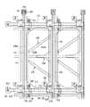
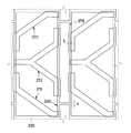
図1は本発明の第1実施例による液晶表示装置用薄膜トランジスタ表示板の配置図であり、図2は本発明の第1実施例による液晶表示装置用色フィルター表示板の配置図であり、図3は本発明の第1実施例による液晶表示装置の配置図であり、図4は図3の液晶表示装置のIV-IV'線の断面図である。 FIG. 1 is a layout diagram of a thin film transistor array panel for a liquid crystal display according to a first embodiment of the present invention, and FIG. 2 is a layout diagram of a color filter panel for a liquid crystal display according to a first embodiment of the present invention. FIG. 3 is a layout view of the liquid crystal display device according to the first embodiment of the present invention, and FIG. 4 is a sectional view taken along line IV-IV ′ of the liquid crystal display device of FIG.
液晶表示装置は、下側の薄膜トランジスタ表示板100、これに対向している上側の対向表示板200及びこれらの間に形成され、2つの表示板100、200に対してほぼ垂直に配向されている液晶分子310を含む液晶層3からなる。 The liquid crystal display device is formed so as to have a lower thin
ガラスなどの透明な絶縁物質からなる薄膜トランジスタ表示板100には、ITO(indium tin oxide)やIZO(indium zinc oxide)などの透明な導電物質からなり、切開部191、192、193を有する画素電極190が形成されており、各画素電極190は、薄膜トランジスタに連結されて画像信号電圧の印加を受ける。この時、薄膜トランジスタは、走査信号を伝達するゲート線121及び画像信号を伝達するデータ線171に各々連結され、走査信号によって画素電極190をオン・オフする。また、薄膜トランジスタ表示板100下面には下部偏光板12が取り付けられている。ここで反射型液晶表示装置の場合には、画素電極190が透明でない物質で形成される場合もあり、その場合には下部偏光板12も不要になる。 A thin
ガラスなどの透明な絶縁物質からなる対向表示板200には、画素の縁で発生する光漏れを防止するためのブラックマトリックス230、赤、緑、青の色フィルター240及びITOまたはIZOなどの透明な導電物質からなる基準電極270が形成されている。ここで、基準電極270には、切開部271、272、273と開口部279とが形成されている。ブラックマトリックス230は、画素領域の周囲部分だけでなく、基準電極270の切開部271、272、273と重畳する部分にも形成することも可能である。これは、切開部271、272、273によって生じる光漏れを防止するためである。 The
それでは、第1実施例による液晶表示装置について詳細に説明する。 Now, the liquid crystal display according to the first embodiment will be described in detail.
薄膜トランジスタ表示板100には、下部絶縁基板110上に横方向にゲート線121が形成されている。ゲート線121には、ゲート電極123が突起状に形成されており、ゲート線121の一端の付近に位置した部分125は外部からのゲート信号をゲート線121に伝達する。絶縁基板110上には、ゲート線121に沿って維持電極線131が形成されている。維持電極線131は、縦方向に形成されている2つの維持電極133a、133bと連結され、これら2つの維持電極133a、133bは横方向に形成されている維持電極133cによって互いに連結されている。この時、維持電極線131は2つ以上設けることもできる。ゲート線121、ゲート電極123、維持電極線131及び維持電極133は、アルミニウムまたはクロムなどの金属で形成される。この時、これらは単一層に形成することもでき、クロム層とアルミニウム層とを連続積層して構成した二重層に形成することもできる。その他にも、多様な金属を用いてゲート配線及び共通配線を形成することができる。 In the thin film
ゲート線121、維持電極線131及び維持電極133a、133b上には、窒化ケイ素(SiNx)などからなるゲート絶縁膜140が形成されている。 A
ゲート絶縁膜140上には、縦方向にデータ線171が形成されている。データ線171には、分枝としてソース電極173が形成され、ソース電極173に隣接してドレーン電極175が形成され、データ線171の一端付近に位置した部分179は外部からの画像信号をデータ線171に伝達する。また、ゲート絶縁膜140上には、データ線171及び重畳橋部金属片172が形成されている。データ線171、ドレーン電極175及び橋部金属片172もゲート線121と同様にクロムやアルミニウムなどの導電物質を含む導電膜で形成し、単一層または多重層に形成することができる。 The data lines 171 are formed on the
ソース電極173及びドレーン電極175下部には、薄膜トランジスタのチャンネル部として用いられる非晶質シリコン層151が形成され、データ線171下にもチャンネル部非晶質シリコン層151が縦に長く連結されている。非晶質シリコン層151上には、ソース及びドレーン電極173、175とチャンネル部非晶質シリコン層151との間の接触抵抗を減少させるための抵抗性接触部材163、165が形成されている。接触部材163もデータ線171に沿ってその下部にのび、n型不純物で高濃度にドーピングされた非晶質シリコンを用いる。 An
データ線171などの上には、窒化ケイ素などの無機絶縁物や樹脂などの有機絶縁物質からなる保護膜180が形成されている。保護膜180には、ドレーン電極175を露出させる接触孔185が形成されている。 A
保護膜180上には、切開部191、192、193を有する画素電極190が形成されている。画素電極190は、ITOやIZOなどのような透明導電体やアルミニウム(Al)のような光反射特性の優れた不透明導電体を用いて形成する。画素電極190に形成されている切開部191、192、193は、画素電極190を上下に両分する位置に横方向に形成されている横切開部192と、両分された画素電極190の上下に各々斜線方向に形成されている斜線開口部191、193とを含む。この時、上下の斜線開口部191、193は互いに垂直をなしている。これは、フリンジフィールドの方向を4方向に均一に分散させるためである。 On the
なお、画素電極190と同一層には、ゲート線121を介して互いに隣接する画素の維持電極133aと維持電極線131とを連結する維持配線連結橋91が形成されている。維持配線連結橋91は、保護膜180とゲート絶縁膜140とにかけて形成されている接触孔183、184を通じて維持電極133a及び維持電極線131に接触している。維持配線連結橋91は、橋部金属片172と重畳しており、これらは互いに電気的に連結されることもできる。維持配線連結橋91は、下部基板110上の維持配線全体を電気的に連結する役割をしている。このような維持配線は、必要に応じてゲート線121やデータ線171の欠陥修理に利用することができ、橋部金属片172は、このような修理のためにレーザーを照射する時にゲート線121と維持配線連結橋91との電気的連結を補助するために形成する。 In the same layer as the
保護膜180上には、ゲート接触補助部材95とデータ接触補助部材97とが形成されている。ゲート接触補助部材95は、保護膜180とゲート絶縁膜140とにかけて形成されている接触孔182を通じてゲート線の端部125に連結されており、データ接触補助部材97は、保護膜180に形成されている接触孔183を通じてデータ線の端部179に連結されている。 A gate contact
対向表示板200には、上部絶縁基板210に画素の縁での光漏れを防止するためのブラックマトリックス230が形成されている。ブラックマトリックス230上には、赤、緑、青の色フィルター240が形成されている。色フィルター230上には、全面的に平坦化膜250が形成され、その上には、切開部271、272、273及び開口部279を有する基準電極270が形成されている。基準電極270は、ITOまたはIZOなどの透明な導電体から形成される。 The opposing
基準電極270の切開部271、272、273は、画素電極190の斜線開口部191、193を間に挟んでおり、これと並ぶ斜線部と画素電極190の辺と重なっている屈折部とを含む。この時、屈折部は縦方向屈折部と横方向屈折部とに分けられる。また、データ線171に対応する基準電極270には、データ線171に沿って複数の開口部279が形成されている。 The
この時、開口部279と切開部271、271、273の縦方向屈折部との間の間隔(b)、及びデータ線171上部で互いに隣接する開口部279の間の間隔(a)は、製造工程における写真エッチング工程で用いられる露光器の解像度より広いのが好ましく、通常3〜6μm以上であるのが良い。このような構造は、開口部279と切開部271、271、273の縦方向屈折部との間の間隔(b)とデータ線171上部で互いに隣接する開口部279の間の間隔(a)とで基準電極270を連結することにより、基準電極270に印加される基準電圧の経路を様々な方向に確保することができる。 At this time, the interval (b) between the
前記のような本発明の実施例の構造では、データ線171と重畳する基準電極270に開口部279を設けることで、データ線に伝達されるデータ信号に対して遅延を最少化することができるので、表示装置の特性を向上させることができる。また、データ線171と基準電極270との間のカップリングによる静電容量を減少させ、データ線171周辺で発生する光漏れ現象を最少化することができる。 In the structure of the embodiment of the present invention as described above, by providing the
以上のような構造の薄膜トランジスタ基板と色フィルター基板とを位置合わせして結合し、その間に液晶物質を注入して垂直配向すれば、本発明による液晶表示装置の基本構造が形成される。薄膜トランジスタ基板と色フィルター基板とを位置合わせする時に、画素電極190の切開部191、192、193と基準電極270の切開部271、272、273とは画素領域を複数の小ドメインに分割する。これらの小ドメインは、その内部に位置する液晶分子の平均長軸方向によって4種類に分類される。 The basic structure of the liquid crystal display device according to the present invention is formed by aligning and coupling the thin film transistor substrate and the color filter substrate having the above-described structure, and injecting a liquid crystal material between them to perform vertical alignment. When aligning the thin film transistor substrate and the color filter substrate, the
次に、このような構造と効果を有する本発明の実施例による液晶表示装置用薄膜トランジスタ表示板を製造する方法について説明する。 Next, a method of manufacturing a TFT array panel for a liquid crystal display having the above-described structure and effects according to an embodiment of the present invention will be described.
まず、基板110上に物理化学的特性が優れたCrまたはMo合金、またはアルミニウムを含む導電膜などを蒸着した後に、マスクを用いた写真エッチング工程でパターニングし、ゲート線121、維持電極133a、133b、及び維持電極線131を形成する。 First, a conductive film including a Cr or Mo alloy or aluminum having excellent physicochemical properties is deposited on the
次に、窒化ケイ素からなるゲート絶縁膜140、非晶質シリコン層、ドーピングされた非晶質シリコン層の3層膜を連続積層し、非晶質シリコン層とドーピングされた非晶質シリコン層とを共にマスクを用いた写真エッチング工程でパターニングし、ゲート電極123上のゲート絶縁膜140上に半導体層151及びその上の抵抗性接触層を形成する(第2マスク)。 Next, three layers of a
次に、CrまたはMo合金、またはアルミニウムまたはアルミニウム合金などの導電膜を蒸着し、マスクを用いた写真エッチング工程でパターニングし、ゲート線121と交差するデータ線171、データ線171と連結されてゲート電極121上部まで延びているソース電極173、及びソース電極173と分離され、ゲート電極121を中心にソース電極173と対向するドレーン電極175を形成する。 Next, a conductive film such as a Cr or Mo alloy or an aluminum or an aluminum alloy is deposited and patterned by a photolithography process using a mask, and the
次に、データ線171及びドレーン電極175によって覆われないドーピングされた非晶質シリコン層をエッチングして、ゲート電極123を中心に両側に位置する抵抗性接触部材163、165を完成し、両側のドーピングされた非晶質シリコン層163、165の間の半導体層151を露出させる。その後、露出された半導体層151の表面を安定化するために酸素プラズマ処理を実施するのが好ましい。 Next, the doped amorphous silicon layer that is not covered by the
次に、a-Si:C:O膜またはa-Si:O:F膜を化学気相蒸着(CVD)法によって成長させたり、窒化ケイ素などの無機絶縁膜を蒸着したり、アクリル系物質などの有機絶縁膜を塗布して、保護膜180を形成する。この時、a-Si:C:O膜の場合には、気体状態のSiH(CH3)3、SiO2(CH3)4、(SiH)4O4(CH3)4、Si(C2H5O)4などを基本ソースとして用いて、N2OまたはO2などの酸化剤とArまたはHeなどとを混合した気体を流しながら蒸着する。また、a-Si:O:F膜の場合には、SiH4、SiF4などにO2を添加した気体を流しながら蒸着する。この時、フッ素の補助ソースとしてCF4を添加することもできる。Next, an a-Si: C: O film or an a-Si: O: F film is grown by a chemical vapor deposition (CVD) method, an inorganic insulating film such as silicon nitride is deposited, an acrylic material, etc. Is applied to form a
次に、写真エッチング工程でゲート絶縁膜140と共に保護膜180をパターニングし、ゲート線の端部125、ドレーン電極175、及びデータ線の端部179を露出する接触孔181、182、183を形成する。ここで、接触孔181、182、183は角のある形状や円形状に形成することもでき、パッド125、179を露出する接触孔125、179の形状寸法は2mm×60μmを超えず、0.5mm×15μm以上であるのが好ましく、接触孔181、182、183の側壁はテーパ構造であるのが好ましい。 Next, the
最後に、ITOまたはIZO膜を蒸着して写真エッチングして、接触孔181を通じてドレーン電極175と連結される画素電極190と、接触孔182、183を通じてゲート線の端部125及びデータ線の端部179と各々連結されるゲート接触補助部材95及びデータ接触補助部材97とを形成する。ITOやIZOを積層する前の予熱(pre-heating)工程で使用する気体としては、窒素が好ましい。これは、接触孔181、182、183を通じて露出されている金属膜上部に金属酸化膜が形成されるのを防止するためである。 Finally, an ITO or IZO layer is deposited and photo-etched, and the
以下、図5及び図6を参照して、本発明の第2実施例による薄膜トランジスタ表示板を含む液晶表示装置の構造について詳細に説明する。 Hereinafter, a structure of a liquid crystal display including a thin film transistor array panel according to a second embodiment of the present invention will be described in detail with reference to FIGS.
図5は本発明の第2実施例による薄膜トランジスタ表示板を含む液晶表示装置の構造を示す配置図であり、図6は図5の液晶表示装置のVI-VI'線の断面図である。 FIG. 5 is a layout view showing a structure of a liquid crystal display device including a thin film transistor panel according to a second embodiment of the present invention, and FIG. 6 is a cross-sectional view taken along line VI-VI 'of the liquid crystal display device of FIG.
図5及び図6に示すように、薄膜トランジスタ表示板には、横方向にのびているゲート線121と縦方向にのびているデータ線171とが交差して画素領域を定義し、各画素領域には、薄膜トランジスタと切開パターン191、192、193、194、195、196、197、198を有する画素電極190とが形成されている。薄膜トランジスタ表示板と対向する対向表示板200には、切開パターン271、272、273、274、275、276、277、278を有する共通電極270が形成されている。画素電極190の切開パターン191、192、193、194、195、196、197、198と共通電極270の切開パターン191、192、193、194、195、196、197、198とは、第1実施例のように、互いに交互に配置され、画素領域を複数の小ドメインに分割する。前記では、ドメイン分割手段として切開パターンを例として挙げたが、突起や溝もドメイン分割手段として使用することができる。 As shown in FIGS. 5 and 6, a pixel region is defined on a thin film transistor array panel by crossing a
図5及び図6のように、本発明の第2実施例による薄膜トランジスタ表示板100は、図3及び図4とほぼ類似している。しかし、複数の線状半導体151及び複数の抵抗性接触部材163、165が備えられている。 As shown in FIGS. 5 and 6, a thin film
線状半導体151は、ソース電極173とドレーン電極175との間にある薄膜トランジスタのチャンネル領域を除けば、複数のデータ線171及び複数のドレーン電極175とほぼ同一の平面形状である。つまり、チャンネル領域においてデータ線171とドレーン電極175とは互いに分離されているが、線状半導体151はここで切れずに連結されて薄膜トランジスタのチャンネル領域を形成する。抵抗性接触部材163、165は、各々データ線171及びドレーン電極175と同一の形状である。 The
ゲート線121、半導体151、及び抵抗性接触部材163、165は、テーパ構造を有する。 The
このような本発明の第2実施例による薄膜トランジスタ表示板の製造方法において、データ線171、ドレーン電極175、及び半導体層151は、1つの感光膜パターンを用いた写真エッチング工程でパターニングする。この時、感光膜パターンは、互いに異なる厚さの第1部分と第2部分とを含むが、第2部分は薄膜トランジスタのチャンネル領域に位置し、第1部分はデータ線及びドレーン電極領域に位置し、第2部分は第1部分より薄い厚さを有する。ここで、第1及び第2部分は半導体層151をパターニングするためのエッチングマスクとして用いられ、第1部分はデータ線及びドレーン電極をパターニングするためのエッチングマスクとして用いられる。このように位置によって感光膜パターンの厚さを異ならせる方法としては様々な方法があるが、例えば、光マスクに透明領域(transparent area)及び遮光領域(light blocking area)の他に半透明領域(translucent area)を設ける方法がある。半透明領域には、スリット(slit)パターン、格子パターン(lattice pattern)、または透過率が中間であるか厚さが中間である薄膜が備えられる。スリットパターンを利用する時には、スリットの幅やスリットの間の間隔が写真工程に用いられる露光器の分解能(resolution)より小さいのが好ましい。その他の例としては、リフローが可能な感光膜を用いる方法がある。つまり、透明領域及び遮光領域だけを有する通常のマスクでリフロー可能な感光膜パターンを形成した後にリフローして、感光膜が残留しない領域に流すことによって、薄い部分を形成するのである。 In the method of manufacturing a thin film transistor array panel according to the second embodiment of the present invention, the
第2実施例の効果は、第1実施例の効果と同一である。つまり、配線の負荷が減少し、配線にかかる液晶容量の変化量が縮少され、側面クロストークによる光漏れが減少して、開口率が増大する。 The effect of the second embodiment is the same as the effect of the first embodiment. That is, the load on the wiring is reduced, the amount of change in the liquid crystal capacitance applied to the wiring is reduced, light leakage due to side crosstalk is reduced, and the aperture ratio is increased.
また、本発明の実施例では、データ線に対応する基準電極に開口部を形成したが、他の実施例では、ゲート線に対応する基準電極に開口部を追加することもできる。 Further, in the embodiment of the present invention, the opening is formed in the reference electrode corresponding to the data line. However, in another embodiment, the opening may be added to the reference electrode corresponding to the gate line.
以上で、本発明の好ましい実施例について詳細に説明したが、本発明の実施例は、該当技術分野の熟練した当業者が、特許請求の範囲に記載された本発明の思想及び領域を超えない範囲内で多様に変形及び改良できることが理解できるであろう。特に、画素電極と共通電極とに形成する切開部の配置は多様に変形することができ、切開部を形成する代わりに突起を設ける等の変形も可能である。 Although the preferred embodiments of the present invention have been described in detail, the embodiments of the present invention do not exceed the spirit and scope of the present invention described in the claims by those skilled in the art. It will be understood that various modifications and improvements can be made within the scope. In particular, the arrangement of the cutouts formed in the pixel electrode and the common electrode can be variously modified, and a modification such as providing a projection instead of forming the cutout is also possible.
121 ゲート線
123 ゲート電極
171 データ線
173 ソース電極
175 ドレーン電極
190 画素電極
191、192、193 切開部
151、153 非晶質シリコン層
270 基準電極
279 開口部121
279 opening
Claims (10)
Translated fromJapanese前記第1基板上に形成されている第1配線と、
前記第1基板上に形成され、前記第1配線と絶縁されて交差している第2配線と、
前記第1配線と前記第2配線とが交差して定義する画素領域ごとに形成され、第1ドメイン分割手段によって複数の小部分に分割されている画素電極と、
前記第1配線、前記第2配線及び前記画素電極と連結されている薄膜トランジスタと、
前記第1基板と対向する絶縁第2基板と、
前記第2基板上に形成され、前記第1ドメイン分割手段と共に前記画素電極を複数の小ドメインに分割する第2ドメイン分割手段と、
前記第2ドメイン分割手段と分離され、前記第1配線または第2配線と重畳する開口部を有する共通電極と、
を含む液晶表示装置。An insulating first substrate;
A first wiring formed on the first substrate;
A second wiring formed on the first substrate and insulated from and crossing the first wiring;
A pixel electrode formed for each pixel region defined by the first wiring and the second wiring crossing each other and divided into a plurality of small parts by a first domain dividing unit;
A thin film transistor connected to the first wiring, the second wiring, and the pixel electrode;
An insulating second substrate facing the first substrate;
A second domain dividing unit formed on the second substrate and dividing the pixel electrode into a plurality of small domains together with the first domain dividing unit;
A common electrode separated from the second domain dividing means and having an opening overlapping with the first wiring or the second wiring;
Liquid crystal display device including.
前記第1基板上の一方向に沿って形成され、ゲート電極を有するゲート線と、
前記ゲート線上に形成されているゲート絶縁膜と、
前記ゲート電極上部の前記ゲート絶縁膜上に形成されている半導体層と、
前記ゲート電極を中心に対向するソース電極及びドレーン電極と前記ソース電極を含み、前記ゲート線と交差するデータ線と、
前記ドレーン電極と連結され、液晶分子を分割配向するための第1切開部を有する画素電極と、
前記第1基板と対向する絶縁第2基板と、
前記第1切開部と共に前記液晶分子を分割配向するための第2切開部と、前記第2切開部と分離され、前記ゲート線またはデータ線上に前記ゲート線またはデータ線に沿って延びている開口部を有する共通電極と、
を含む液晶表示装置。An insulating first substrate;
A gate line formed along one direction on the first substrate and having a gate electrode;
A gate insulating film formed on the gate line;
A semiconductor layer formed on the gate insulating film above the gate electrode;
Including a source electrode and a drain electrode facing the gate electrode and the source electrode, and a data line crossing the gate line;
A pixel electrode connected to the drain electrode and having a first cutout for dividing and aligning liquid crystal molecules;
An insulating second substrate facing the first substrate;
A second cutout for dividing and orienting the liquid crystal molecules together with the first cutout, and an opening separated from the second cutout and extending over the gate line or the data line along the gate line or the data line; A common electrode having a portion;
Liquid crystal display device including.
Applications Claiming Priority (1)
| Application Number | Priority Date | Filing Date | Title |
|---|---|---|---|
| KR1020030030195AKR100961946B1 (en) | 2003-05-13 | 2003-05-13 | Vertically Aligned Liquid Crystal Display |
Publications (1)
| Publication Number | Publication Date |
|---|---|
| JP2004341530Atrue JP2004341530A (en) | 2004-12-02 |
Family
ID=33411702
Family Applications (1)
| Application Number | Title | Priority Date | Filing Date |
|---|---|---|---|
| JP2004144019APendingJP2004341530A (en) | 2003-05-13 | 2004-05-13 | Vertical alignment type liquid crystal display |
Country Status (5)
| Country | Link |
|---|---|
| US (2) | US7110075B2 (en) |
| JP (1) | JP2004341530A (en) |
| KR (1) | KR100961946B1 (en) |
| CN (1) | CN100432803C (en) |
| TW (1) | TWI291234B (en) |
Cited By (6)
| Publication number | Priority date | Publication date | Assignee | Title |
|---|---|---|---|---|
| JP2006201344A (en)* | 2005-01-19 | 2006-08-03 | Sharp Corp | Substrate for liquid crystal display device and liquid crystal display device |
| JP2010128045A (en)* | 2008-11-26 | 2010-06-10 | Toppan Printing Co Ltd | Color filter and liquid crystal display device with the same |
| JP2011048396A (en)* | 2010-12-06 | 2011-03-10 | Sharp Corp | Substrate for display device and display device |
| US8610863B2 (en) | 2007-02-01 | 2013-12-17 | Samsung Display Co., Ltd. | Liquid crystal display panel |
| JP2015018182A (en)* | 2013-07-12 | 2015-01-29 | スタンレー電気株式会社 | Liquid crystal display |
| JP2024096185A (en)* | 2006-06-02 | 2024-07-12 | 株式会社半導体エネルギー研究所 | Liquid crystal display device |
Families Citing this family (36)
| Publication number | Priority date | Publication date | Assignee | Title |
|---|---|---|---|---|
| KR101061844B1 (en)* | 2004-06-29 | 2011-09-02 | 삼성전자주식회사 | Manufacturing method of thin film display panel |
| KR101160825B1 (en)* | 2004-08-18 | 2012-06-29 | 삼성전자주식회사 | Liquid crystal display |
| KR101061848B1 (en)* | 2004-09-09 | 2011-09-02 | 삼성전자주식회사 | Thin film transistor panel and multi-domain liquid crystal display including the same |
| US7639333B2 (en) | 2005-04-06 | 2009-12-29 | Samsung Electronics Co., Ltd. | Display panel and liquid crystal display apparatus including the same |
| KR101189270B1 (en)* | 2005-04-06 | 2012-10-15 | 삼성디스플레이 주식회사 | Panel and liquid crystal display includig the same |
| KR20060116878A (en)* | 2005-05-11 | 2006-11-15 | 삼성전자주식회사 | Display substrate, manufacturing method thereof and liquid crystal display device having same |
| KR101251994B1 (en)* | 2005-07-01 | 2013-04-08 | 삼성디스플레이 주식회사 | Liquid crystal display |
| US7656487B2 (en) | 2005-07-01 | 2010-02-02 | Samsung Electronics Co., Ltd. | Liquid crystal display |
| KR101261611B1 (en)* | 2005-09-15 | 2013-05-06 | 삼성디스플레이 주식회사 | Liquid crystal display |
| KR100643376B1 (en)* | 2005-10-24 | 2006-11-10 | 삼성전자주식회사 | Display device and manufacturing method |
| KR101279189B1 (en)* | 2005-11-10 | 2013-07-05 | 엘지디스플레이 주식회사 | Liquid crystal display device of horizontal electronic field applying type and fabricating method thereof |
| KR101251996B1 (en)* | 2005-12-07 | 2013-04-08 | 삼성디스플레이 주식회사 | Liquid crystal display |
| CN101038407B (en)* | 2006-03-17 | 2010-09-08 | 奇美电子股份有限公司 | Multi-display domain vertical alignment type liquid crystal display panel |
| KR101189090B1 (en)* | 2006-07-18 | 2012-11-09 | 삼성디스플레이 주식회사 | LCD and its driving method |
| KR101282402B1 (en)* | 2006-09-15 | 2013-07-04 | 삼성디스플레이 주식회사 | Liquid crystal display device |
| JP4606497B2 (en)* | 2006-09-29 | 2011-01-05 | シャープ株式会社 | Display device |
| TWI349138B (en)* | 2006-12-29 | 2011-09-21 | Chimei Innolux Corp | Multi-domain vertical alignment liquid crystal panel |
| TWI342428B (en)* | 2006-12-29 | 2011-05-21 | Chimei Innolux Corp | Mva liquid crystal display panel |
| CN101652805B (en)* | 2007-04-23 | 2011-06-15 | 夏普株式会社 | Display device, method of manufacturing display device |
| CN101354508B (en)* | 2007-07-23 | 2010-06-02 | 中华映管股份有限公司 | Liquid crystal display panel |
| KR20100005883A (en)* | 2008-07-08 | 2010-01-18 | 삼성전자주식회사 | Array substrate and liquid crystal display apparatus having the same |
| KR20100008566A (en)* | 2008-07-16 | 2010-01-26 | 삼성전자주식회사 | Liquid crystal display |
| KR101539953B1 (en)* | 2008-12-04 | 2015-07-29 | 삼성디스플레이 주식회사 | Liquid crystal display |
| KR101722501B1 (en)* | 2009-01-09 | 2017-04-04 | 삼성디스플레이 주식회사 | Thin film transistor and liquid crystal display having the same |
| US8411239B2 (en) | 2009-02-13 | 2013-04-02 | Sharp Kabushiki Kaisha | Array substrate, liquid crystal display device, electronic device |
| CN101840099B (en)* | 2009-03-18 | 2012-12-26 | 北京京东方光电科技有限公司 | Liquid crystal display panel and manufacture method thereof |
| KR101791579B1 (en)* | 2011-04-08 | 2017-10-31 | 삼성디스플레이 주식회사 | Liquid crystal display |
| JP5572603B2 (en)* | 2011-08-30 | 2014-08-13 | 株式会社ジャパンディスプレイ | Liquid crystal display |
| US9570365B2 (en) | 2014-03-14 | 2017-02-14 | Innolux Corporation | Display device and test pad thereof |
| US9750140B2 (en) | 2014-03-14 | 2017-08-29 | Innolux Corporation | Display device |
| US10324345B2 (en) | 2014-03-14 | 2019-06-18 | Innolux Corporation | Display device and display substrate |
| US9507222B2 (en) | 2014-03-14 | 2016-11-29 | Innolux Corporation | Display device |
| TWI537656B (en) | 2014-03-14 | 2016-06-11 | 群創光電股份有限公司 | Display device |
| US9659973B2 (en) | 2014-03-14 | 2017-05-23 | Innolux Corporation | Display device |
| US9513514B2 (en) | 2014-03-14 | 2016-12-06 | Innolux Corporation | Display device |
| CN113721395B (en)* | 2021-08-25 | 2022-09-09 | Tcl华星光电技术有限公司 | Display panel and display device |
Citations (4)
| Publication number | Priority date | Publication date | Assignee | Title |
|---|---|---|---|---|
| JPH06118447A (en)* | 1992-10-06 | 1994-04-28 | Sony Corp | Liquid crystal panel |
| JPH08286207A (en)* | 1995-04-14 | 1996-11-01 | Casio Comput Co Ltd | Liquid crystal display element |
| JP2001109009A (en)* | 1999-10-01 | 2001-04-20 | Samsung Electronics Co Ltd | Wide viewing angle LCD |
| JP2001343647A (en)* | 2000-05-30 | 2001-12-14 | Sharp Corp | Liquid crystal display device and manufacturing method thereof |
Family Cites Families (6)
| Publication number | Priority date | Publication date | Assignee | Title |
|---|---|---|---|---|
| KR100293809B1 (en)* | 1998-05-29 | 2001-10-26 | 박종섭 | IP-V Mode LCD Display with Multiple Domains |
| CN1139837C (en)* | 1998-10-01 | 2004-02-25 | 三星电子株式会社 | Film transistor array substrate for liquid crystal display and manufacture thereof |
| KR100357216B1 (en)* | 1999-03-09 | 2002-10-18 | 엘지.필립스 엘시디 주식회사 | Multi-domain liquid crystal display device |
| KR100635940B1 (en)* | 1999-10-29 | 2006-10-18 | 삼성전자주식회사 | Vertically Aligned Liquid Crystal Display |
| KR100366770B1 (en)* | 2001-04-06 | 2003-01-06 | 삼성전자 주식회사 | a liquid crystal display |
| KR100759978B1 (en)* | 2001-07-12 | 2007-09-18 | 삼성전자주식회사 | Vertically oriented liquid crystal display device and color filter substrate used therein |
- 2003
- 2003-05-13KRKR1020030030195Apatent/KR100961946B1/ennot_activeExpired - Fee Related
- 2004
- 2004-05-12USUS10/844,239patent/US7110075B2/ennot_activeExpired - Fee Related
- 2004-05-13JPJP2004144019Apatent/JP2004341530A/enactivePending
- 2004-05-13TWTW093113530Apatent/TWI291234B/ennot_activeIP Right Cessation
- 2004-05-13CNCNB2004100631575Apatent/CN100432803C/ennot_activeExpired - Fee Related
- 2006
- 2006-09-19USUS11/523,302patent/US7379142B2/ennot_activeExpired - Fee Related
Patent Citations (4)
| Publication number | Priority date | Publication date | Assignee | Title |
|---|---|---|---|---|
| JPH06118447A (en)* | 1992-10-06 | 1994-04-28 | Sony Corp | Liquid crystal panel |
| JPH08286207A (en)* | 1995-04-14 | 1996-11-01 | Casio Comput Co Ltd | Liquid crystal display element |
| JP2001109009A (en)* | 1999-10-01 | 2001-04-20 | Samsung Electronics Co Ltd | Wide viewing angle LCD |
| JP2001343647A (en)* | 2000-05-30 | 2001-12-14 | Sharp Corp | Liquid crystal display device and manufacturing method thereof |
Cited By (6)
| Publication number | Priority date | Publication date | Assignee | Title |
|---|---|---|---|---|
| JP2006201344A (en)* | 2005-01-19 | 2006-08-03 | Sharp Corp | Substrate for liquid crystal display device and liquid crystal display device |
| JP2024096185A (en)* | 2006-06-02 | 2024-07-12 | 株式会社半導体エネルギー研究所 | Liquid crystal display device |
| US8610863B2 (en) | 2007-02-01 | 2013-12-17 | Samsung Display Co., Ltd. | Liquid crystal display panel |
| JP2010128045A (en)* | 2008-11-26 | 2010-06-10 | Toppan Printing Co Ltd | Color filter and liquid crystal display device with the same |
| JP2011048396A (en)* | 2010-12-06 | 2011-03-10 | Sharp Corp | Substrate for display device and display device |
| JP2015018182A (en)* | 2013-07-12 | 2015-01-29 | スタンレー電気株式会社 | Liquid crystal display |
Also Published As
| Publication number | Publication date |
|---|---|
| KR100961946B1 (en) | 2010-06-10 |
| US20040227888A1 (en) | 2004-11-18 |
| KR20040097765A (en) | 2004-11-18 |
| TW200527679A (en) | 2005-08-16 |
| CN1550862A (en) | 2004-12-01 |
| TWI291234B (en) | 2007-12-11 |
| US20070008475A1 (en) | 2007-01-11 |
| US7379142B2 (en) | 2008-05-27 |
| CN100432803C (en) | 2008-11-12 |
| US7110075B2 (en) | 2006-09-19 |
Similar Documents
| Publication | Publication Date | Title |
|---|---|---|
| JP2004341530A (en) | Vertical alignment type liquid crystal display | |
| US6940573B2 (en) | Liquid crystal display and thin film transistor array panel | |
| US7782436B2 (en) | Liquid crystal display device | |
| US7889304B2 (en) | Liquid crystal display and fabricating method thereof | |
| JP4638221B2 (en) | Vertical alignment type liquid crystal display device | |
| TWI451155B (en) | Liquid crystal display device and fabricating method thereof | |
| US7206054B2 (en) | LCD with bent split pixel electrodes with transistor for each partition | |
| JP2006195455A (en) | Thin film transistor display panel | |
| US20010024247A1 (en) | Active matrix substrate and manufacturing method thereof | |
| US20060232721A1 (en) | Liquid crystal display and thin film transistor array panel | |
| JP2009218604A (en) | Production method of thin film transistor display panel | |
| KR20060040058A (en) | Multi Domain Thin Film Transistor Display Panel | |
| US20060131581A1 (en) | Thin film transistor array panel and method for manufacturing the same | |
| KR20040099749A (en) | Multi-domain liquid crystal display | |
| JP4782389B2 (en) | Display panel for display device and liquid crystal display device including the display panel | |
| JP2005182048A (en) | Multi-domain thin film transistor array panel and liquid crystal display device including the same | |
| KR101061856B1 (en) | Thin film transistor array panel | |
| JP2009151285A (en) | Liquid crystal display device and method for manufacturing the same | |
| CN100458533C (en) | Thin film transistor array panel and manufacturing method thereof | |
| US8294862B2 (en) | Liquid crystal display device and method of fabricating the same | |
| KR20050038116A (en) | Panel for liquid crystal display device and method for fabricating the same | |
| KR20070072275A (en) | Vertical alignment liquid crystal display device and manufacturing method thereof | |
| KR20060016502A (en) | Liquid crystal display device, color filter display panel and manufacturing method thereof | |
| KR20050082666A (en) | Thin film transistor panel and liquid crystal display including the panel | |
| KR20060074554A (en) | Thin film transistor array panel |
Legal Events
| Date | Code | Title | Description |
|---|---|---|---|
| A621 | Written request for application examination | Free format text:JAPANESE INTERMEDIATE CODE: A621 Effective date:20060518 | |
| A131 | Notification of reasons for refusal | Free format text:JAPANESE INTERMEDIATE CODE: A131 Effective date:20090630 | |
| A521 | Written amendment | Free format text:JAPANESE INTERMEDIATE CODE: A523 Effective date:20090911 | |
| A131 | Notification of reasons for refusal | Free format text:JAPANESE INTERMEDIATE CODE: A131 Effective date:20100302 | |
| A601 | Written request for extension of time | Free format text:JAPANESE INTERMEDIATE CODE: A601 Effective date:20100601 | |
| A602 | Written permission of extension of time | Free format text:JAPANESE INTERMEDIATE CODE: A602 Effective date:20100604 | |
| A521 | Written amendment | Free format text:JAPANESE INTERMEDIATE CODE: A523 Effective date:20100625 | |
| A02 | Decision of refusal | Free format text:JAPANESE INTERMEDIATE CODE: A02 Effective date:20101214 | |
| A521 | Written amendment | Free format text:JAPANESE INTERMEDIATE CODE: A523 Effective date:20110331 | |
| A911 | Transfer to examiner for re-examination before appeal (zenchi) | Free format text:JAPANESE INTERMEDIATE CODE: A911 Effective date:20110407 | |
| A912 | Re-examination (zenchi) completed and case transferred to appeal board | Free format text:JAPANESE INTERMEDIATE CODE: A912 Effective date:20110513 |