JP2004340702A - Microchip and liquid detection method - Google Patents
Microchip and liquid detection methodDownload PDFInfo
- Publication number
- JP2004340702A JP2004340702AJP2003136766AJP2003136766AJP2004340702AJP 2004340702 AJP2004340702 AJP 2004340702AJP 2003136766 AJP2003136766 AJP 2003136766AJP 2003136766 AJP2003136766 AJP 2003136766AJP 2004340702 AJP2004340702 AJP 2004340702A
- Authority
- JP
- Japan
- Prior art keywords
- light
- microchannel
- liquid
- scattering surface
- microchip
- Prior art date
- Legal status (The legal status is an assumption and is not a legal conclusion. Google has not performed a legal analysis and makes no representation as to the accuracy of the status listed.)
- Pending
Links
- 239000007788liquidSubstances0.000titleclaimsabstractdescription61
- 238000001514detection methodMethods0.000titleabstractdescription28
- 239000000758substrateSubstances0.000claimsabstractdescription66
- 238000000149argon plasma sinteringMethods0.000claimsabstractdescription51
- 238000007789sealingMethods0.000claimsabstractdescription8
- 238000000034methodMethods0.000claimsdescription18
- 230000001678irradiating effectEffects0.000claims6
- 229920000435poly(dimethylsiloxane)Polymers0.000description24
- 239000004205dimethyl polysiloxaneSubstances0.000description23
- 239000006061abrasive grainSubstances0.000description8
- XLYOFNOQVPJJNP-UHFFFAOYSA-NwaterChemical compoundOXLYOFNOQVPJJNP-UHFFFAOYSA-N0.000description6
- 238000004458analytical methodMethods0.000description5
- 238000006243chemical reactionMethods0.000description5
- 239000000463materialSubstances0.000description5
- 230000003746surface roughnessEffects0.000description5
- XUIMIQQOPSSXEZ-UHFFFAOYSA-NSiliconChemical compound[Si]XUIMIQQOPSSXEZ-UHFFFAOYSA-N0.000description4
- 230000007423decreaseEffects0.000description4
- 229920003229poly(methyl methacrylate)Polymers0.000description4
- 239000004926polymethyl methacrylateSubstances0.000description4
- 229910052710siliconInorganic materials0.000description4
- 239000010703siliconSubstances0.000description4
- 239000000126substanceSubstances0.000description4
- KFZMGEQAYNKOFK-UHFFFAOYSA-NIsopropanolChemical compoundCC(C)OKFZMGEQAYNKOFK-UHFFFAOYSA-N0.000description3
- 239000011521glassSubstances0.000description3
- 238000004519manufacturing processMethods0.000description3
- 230000035945sensitivityEffects0.000description3
- 238000005266castingMethods0.000description2
- 239000003795chemical substances by applicationSubstances0.000description2
- 238000005520cutting processMethods0.000description2
- 238000010586diagramMethods0.000description2
- 238000005516engineering processMethods0.000description2
- NBVXSUQYWXRMNV-UHFFFAOYSA-NfluoromethaneChemical compoundFCNBVXSUQYWXRMNV-UHFFFAOYSA-N0.000description2
- 239000000203mixtureSubstances0.000description2
- 238000000465mouldingMethods0.000description2
- 230000003287optical effectEffects0.000description2
- 238000001020plasma etchingMethods0.000description2
- 239000011347resinSubstances0.000description2
- 229920005989resinPolymers0.000description2
- 238000007788rougheningMethods0.000description2
- 239000004576sandSubstances0.000description2
- 239000000243solutionSubstances0.000description2
- 240000007049Juglans regiaSpecies0.000description1
- 235000009496Juglans regiaNutrition0.000description1
- 230000015572biosynthetic processEffects0.000description1
- 239000000919ceramicSubstances0.000description1
- 239000003153chemical reaction reagentSubstances0.000description1
- 238000003759clinical diagnosisMethods0.000description1
- 239000011248coating agentSubstances0.000description1
- 238000000576coating methodMethods0.000description1
- 229910021540colemaniteInorganic materials0.000description1
- 238000011109contaminationMethods0.000description1
- 230000006866deteriorationEffects0.000description1
- 238000011161developmentMethods0.000description1
- 239000012153distilled waterSubstances0.000description1
- 238000007877drug screeningMethods0.000description1
- 230000000694effectsEffects0.000description1
- 229920001971elastomerPolymers0.000description1
- 239000000806elastomerSubstances0.000description1
- 230000007613environmental effectEffects0.000description1
- 238000005530etchingMethods0.000description1
- 238000000605extractionMethods0.000description1
- 239000012467final productSubstances0.000description1
- 238000010030laminatingMethods0.000description1
- 238000003754machiningMethods0.000description1
- 238000005259measurementMethods0.000description1
- 239000011259mixed solutionSubstances0.000description1
- 238000012544monitoring processMethods0.000description1
- 239000003960organic solventSubstances0.000description1
- 239000002245particleSubstances0.000description1
- 229920002120photoresistant polymerPolymers0.000description1
- -1polydimethylsiloxanePolymers0.000description1
- 108090000623proteins and genesProteins0.000description1
- 238000000746purificationMethods0.000description1
- 238000005096rolling processMethods0.000description1
- 229920002379silicone rubberPolymers0.000description1
- 238000004381surface treatmentMethods0.000description1
- 238000003786synthesis reactionMethods0.000description1
- 238000012360testing methodMethods0.000description1
- 238000002834transmittanceMethods0.000description1
- 230000000007visual effectEffects0.000description1
- 235000020234walnutNutrition0.000description1
Images


Landscapes
- Optical Measuring Cells (AREA)
- Automatic Analysis And Handling Materials Therefor (AREA)
- Geophysics And Detection Of Objects (AREA)
- Micromachines (AREA)
Abstract
Description
Translated fromJapanese【0001】
【発明の属する技術分野】
本発明はマイクロチップに関する。更に詳細には、本発明は透明基板内にキャピラリチャネルや反応ポートなどの極微細構造を有するマイクロチップ及びそのキャピラリチャネルや反応ポートなどの内部の透明な液体の存在の有無を検出する方法に関する。
【0002】
【従来の技術】
最近、マイクロスケール・トータル・アナリシス・システムズ(μTAS)又はラブ・オン・チップ(Lab−on−Chip)などの名称で知られるように、基板内に所定の形状の流路を構成するマイクロチャネル及び反応ポートなどの微細構造を設け、該微細構造内で物質の化学反応、合成、精製、抽出、生成及び/又は分析など各種の操作を行うことが提案され、一部実用化されている。このような目的のために製作された、基板内にマイクロチャネル及び反応ポートなどの微細構造を有する構造物は総称して「マイクロチップ」と呼ばれる。
【0003】
マイクロチップは遺伝子解析、臨床診断、薬物スクリーニング及び環境モニタリングなどの幅広い用途に使用できる。常用サイズの同種の装置に比べて、マイクロチップは▲1▼サンプル及び試薬の使用量が著しく少ない、▲2▼分析時間が短い、▲3▼感度が高い、▲4▼現場に携帯し、その場で分析できる、及び▲5▼使い捨てできるなどの利点を有する。
【0004】
マイクロチップの材質や構造及び製造方法は例えば、特許文献1、特許文献2及び非特許文献1などに提案されている。図8に示されるように、マイクロチップ100は基本的に、透明基板102と、この透明基板102内に設けられたマイクロチャネル104を封止する対面基板110とからなる。また、透明基板102には前記マイクロチャネル104に連通するホール106,108が開設されている。しかし、場合により、ホール106,108は対面基板110に配設されることもある。
【0005】
透明基板102の形成材料としては前記各文献に開示されているように、例えば、エラストマータイプのシリコン樹脂であるPDMS(ポリジメチルシロキサン)が使用される。PDMSは良好なモールド転写性や透明性、耐薬品性、生体適合性などマイクロチップの部材として優れた特徴を有する。従って、PDMSにより形成されたマイクロチップは、微細構造たるマイクロチャネルを形成する際に、作業が繁雑なエッチングや、切削などの機械加工などの処理プロセスが不要であり、単純かつ安価な型取りと封止だけで極めて簡単にマイクロチャネルを形成することができる。PDMS以外の透明基板材料(例えば、ガラス又はポリメチルメタクリレート(PMMA)など)も同様に使用できる。
【0006】
【特許文献1】
特開2001−157855号公報
【特許文献2】
米国特許第5965237号明細書
【非特許文献1】
David C. Duffy et al, Rapid Prototyping of Microfluidic Systems in Poly(dimethylsiloxane), Analytical Chemistry, Vol.70, No.23, December 1, 1988, pp.4974−4984
【0007】
【発明が解決しようとする課題】
しかし、透明基板102に形成されたマイクロチャネル104の管路径は一般的に、数μm〜数百μm程度の範囲内である。従って、このような微細な流路を流れる薬液などの液体の目視による検出は、管路径が極微小であるばかりか、扱われる液体の量が極微量であるため極めて困難である。特に、薬液が透明な液体である場合、マイクロチャネル内におけるその有無を目視で確認することは殆ど不可能に近い。しかも、マイクロチャネル内における透明な液体の有無を目視以外の手段により簡便に検出する方法は未だ開発されていない。今後、マイクロチップなどの技術が広く普及していくにつれて、マイクロチャネル内の透明液体を簡便に、かつ確実に検出することは、マイクロチップを用いた分析の自動化や装置化を行う上で絶対的に必要な技術となってくる。
【0008】
従って、本発明の目的は、マイクロチャネル内の液体の有無を容易に検出することができるマイクロチップ及びその液体検出方法を提供することである。
【0009】
【課題を解決するための手段】
前記課題は、一方の表面に所定の形状の流路を構成するマイクロチャネルが配設された透明基板と、該マイクロチャネルを封止する透明対面基板とからなるマイクロチップにおいて、前記マイクロチャネルの内壁面の少なくとも一部に、光の散乱が発生するような微細な凹凸を形成した光散乱面を設け、その光散乱面の透過光又は反射光の強度により液体の有無を検出することにより解決される。
【0010】
【発明の実施の形態】
以下、図面を参照しながら本発明のマイクロチップ及び該マイクロチップにおける液体検出方法を具体的に説明する。
【0011】
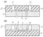
図1は本発明のマイクロチップの部分概要断面図である。図1において、本発明のマイクロチップ1は従来のマイクロチップと同様に、PDMSなどのような光を透過する透明な基板3の一方の面に、所定の形状の流路を構成するマイクロチャネル5が形成されており、このマイクロチャネル5を封止する透明対面基板7が前記基板3のマイクロチャネル5形成面に接合されている。本発明のマイクロチップ1は従来のマイクロチップと異なり、マイクロチャネル5の内壁面(例えば、上面)の少なくとも一部に、光の散乱が発生するような微細な凹凸を有する光散乱面9が形成されている。透明対面基板7は例えば、PDMS、ガラス、ポリメチルメタクリレート(PMMA)などから形成されている。図1において、(A)は透明基板3に、マイクロチャネル5と連通するホール11及び13が形成されている実施態様を示し、(B)は透明対面基板7にホール11及び13が形成されている実施態様を示す。説明の便宜上、下記においては、図1(A)の実施態様に係わるマイクロチップ1について説明する。
【0012】
図2は図1(A)に示されたマイクロチャネル5の部分平面図である。図2のドット面が光散乱面9である。光散乱面9はマイクロチャネル5の内壁面の一部分に形成することもできるが、マイクロチャネル5の内壁面の全てに形成することもできる。光散乱面9をマイクロチャネル5の内壁面の一部分に形成する場合、マイクロチャネル5内に流された液体が光散乱面9の部分にまで達しているか否かを検出するのに利用することができる。一方、光散乱面9をマイクロチャネル5の内壁面の全てに形成する場合、マイクロチャネル5内に流された液体に気泡が含まれているか否かを検出するのに利用できる。マイクロチャネル5において、光散乱面9が形成される部分は、図2に示されるようにマイクロチャネル5の他の部分の内径又は幅に比べて大きくすることができる。このように内径拡大部分に光散乱面9を設けることにより散乱光検出操作を容易にしたり、検出感度を上げることができる。しかし、特別に内径拡大部分を設けること無く、一定の幅のマイクロチャネル5の内壁面に光散乱面9を設けることもできる。図2では、マイクロチャネル5の上面に光散乱面9が配設されているが、側壁面に光散乱面9を設けることもできる。
【0013】
図3は図1に示されたマイクロチャネル5の製造方法を示す工程図である。先ず、ステップ(a)において、最終製品のマイクロチップ1のサイズ(例えば、20mmx20mm又は20mmx30mm)と概ね同じサイズのシリコンウエハ15を準備する。シリコンウエハ15は予め乾燥させたり、表面処理などの所望の前処理を施すこともできる。その後、ステップ(b)において、適当なレジスト材料(例えば、ネガティブフォトレジストSU−8など)を2000rpm〜5000rpmの回転速度で数秒間〜数十秒間にわたってスピン塗布し、オーブン中で乾燥させ、所望の厚さのレジスト膜17を形成する。次いで、ステップ(c)において、レジスト膜17上に第1のマスクパターン19を載置し、この第1のマスク19の上部から、サンドブラスター21により砥粒23を吹き付ける。第1のマスク19には所定の箇所に開口部25が配設されており、この開口部25を通して、下部のレジスト膜17の上面が砥粒23により粗面化される。この粗面化は例えば、砂、コールマン石、セラミック又は破砕クルミ殻などの砥粒を用いて実施することができる。砥粒の粒径は例えば、数μm〜数百μmの範囲内であることが好ましい。サンドブラスター21からの砥粒吐出圧力は例えば、約数KPa〜約数千KPaの範囲内であり、また、砥粒は約数g/分〜数千g/分の供給速度で吐出することが好ましい。このような砥粒23の吐出によりレジスト膜17の該当個所を平均表面粗さ約数十nm、表面粗さ約数十nm〜数μmの範囲内で粗面化させることができる。別法として、所定の表面粗さを有する梨地ローラ(図示されていない)をレジスト膜17の所望の個所で転圧することにより、該表面を粗面化させることもできる。その後、ステップ(d)において、第1のマスク19を除去すると、所望の箇所に粗面部27を有するレジスト膜17が得られる。次いで、ステップ(e)において、このレジスト膜17上に第2のマスク28を通して、適当な露光装置(図示されていない)で露光する。第2のマスク28は本発明のマイクロチップ1におけるマイクロチャネル5に対応するレイアウトパターンを有する。その後、ステップ(f)において、適当な現像液(例えば、1−メトキシ−2−プロピル酢酸)中で現像し、上面にマイクロチャネル5に対応する微細構造29を有するマスター30を生成する。微細構造29の所定箇所には粗面部27がそのまま残置されている。所望により、このマスター30を有機溶媒(例えば、イソプロピルアルコール)及び蒸留水で洗浄することができる。更に、マスター30の表面をフルオロカーボンの存在下で反応性イオンエッチングシステムにより処理することができる。このフルオロカーボン存在下の反応性イオンエッチング処理は、後のステップにおいて、PDMSのマスター30からの離型性を改善する。次いで、ステップ(g)において、前記のマスター30の上面に、PDMSプレポリマーと硬化剤を適度な割合で混合し、脱気したPDMSプレポリマー混合液を流し込む。この際、型枠を使用し、鋳込み型とし、その中にPDMSプレポリマー混合液を流し込んで型取りすることが好ましい。PDMSプレポリマー混合液としては、例えば、米国のダウ・コーニング社製のSYLGARD 184 SILICONE ELASTOMERが好適に使用できる。これは液状のPDMSプレポリマーと硬化剤を10対1の割合で混合するものである。塗布後、常温で十分な時間放置するか、又は、例えばオーブン中で65℃で1時間加熱するか若しくは135℃で15分間加熱して硬化させ、PDMS基板3を生成させる。PDMS基板3は透明性の高いゴム状の樹脂であり、マスター30の微細構造29が転写されている。その後、ステップ(h)において、PDMS基板3をマスター30から剥離し、対面基板7に貼り合わせる。最後に、ステップ(i)において、PDMS基板3の上面から下部のマイクロチャネル5に連通するホール11及び13を穿設し、本発明のマイクロチップ1を得る。別法として、ステップ(h)において、PDMS基板3の上面から下部のマイクロチャネル5に連通するホール11及び13を穿設してから、マスター30から剥離し、最後に、ステップ(i)において、透明対面基板7に貼り合わせて、本発明のマイクロチップ1を得ることもできる。
【0014】
図4は本発明のマイクロチャネル5内の液体検出方法の第1の実施態様を示す概念図である。本発明のマイクロチップ1のマイクロチャネル5内の液体検出部位(すなわち、光散乱面9が形成されている部位)に対応する透明基板3の上部に投光器31を配置し、その対応する対面基板7の下部に受光器33を配置する。別法として、透明基板3の上部に受光器33を配置し、その対応する対面基板7の下部に投光器31を配置することもできる。投光器31は光源(図示されていない)と、必要に応じて光線を所定の直径の平行光に収束させるためのコリメータレンズ及び/又は収束レンズを有する。光源としては可視光、赤外光、紫外光又はレーザ光などを適宜使用することができる。PDMSの透過光の波長は300〜1100nmの範囲でほぼ可視光全域をカバーするので、光源としては可視光を放射する発光ダイオード(LED)が好ましい。受光器33は、適当な光学系と受光素子とから構成される。受光素子としては、アバランシェフォトダイオード(APD)、フォトダイオード(PD)、電荷結合素子(CCD)又はホトマルチプライヤーなどが好ましい。比較的安価であり、しかも感度が高い点で、受光器33としてはアバランシェフォトダイオード(APD)が特に好ましい。受光器33を構成する光学系は例えば、集光レンズなどである。集光レンズとしては常用の対物レンズ又は屈折率分布型レンズなどを適宜使用することができる。受光器33は光検出回路35に接続されている。受光器33で受光された光は、先ず光検出回路35のプリアンプ37で増幅され、次いで、コンパレータ39で基準値(例えば、液体が存在しない場合の透過光強度値及び液体が存在する場合の透過光強度値)と比較される。コンパレータ39にはノイズをカットするための閾値電圧調整回路41が接続されている。コンパレータ39の結果はLED駆動回路43に送信され、LED45を点灯させることにより検出結果を目視可能に表示する。言うまでもなく、光検出回路35の構成は前記のような構成に限定されない。例えば、受光器33で受光した透過光をA/D変換器で電気信号に変換し、その強度を検出レベルメータで示すことによっても液体の有無を判定することができる。
【0015】
マイクロチャネル5内に流される液体が、投光器31の照射する光の波長に対して十分に透明であり、かつ、透明基板3及び対面基板7とその光に対する屈折率が同じか又はほぼ同等であるとすると、マイクロチャネル5内に液体が存在しない場合、投光器31からの照射光47は光散乱面9の凹凸により散乱されて散乱光49となり、受光器33に入射する透過光51は少なくなる。その結果、受光器33で検出される光の強度は低くなる。一方、マイクロチャネル5内に液体が存在する場合、液体は流れていても、静止していてもどちらでも差し支えないが、光散乱面9の凹凸に液体が入り込み、光散乱面9は光学的にほぼ一様な材質となる。そのため、光の散乱は無くなるか、又は軽減され、結果的に受光器33で検出される透過光の強度は高くなる。従って、受光器33が受光する光の強度を調べることにより、マイクロチャネル5内の液体の有無を検出することができる。
【0016】
透明基板3は複数枚積層させて使用することができる。図5はこのような複数枚の透明基板3a,3b,3cを有するマイクロチップ1における本発明の液体検出方法の第2の実施態様を示す概念図である。図5に示されるように、各透明基板3a,3b,3cの各マイクロチャネル5a,5b,5cの各光散乱面9a,9b,9cが同一直線上に整列するように設けられている。本発明によれば、この光散乱面に対応する位置に投光器31及び受光器33を配置し、各マイクロチャネル5a,5b,5cの光散乱面を通過する透過光の強度を検出することができる。前記図4に示された実施態様と同じ原理から、マイクロチャネル5a,5b,5cの何れか一つでも液体が満たされていない場合は、光散乱面で入射光が散乱されるために受光器33で検出される透過光の強度は低くなる。反対に、全てのマイクロチャネルが液体で満たされいる場合は、入射光の散乱は生じないので透過光強度は高くなる。従って、この実施態様によれば、受光器33で受光される光の強度を調べることにより、全てのマイクロチャネルに液体が満たされているか否かを検出することができる。
【0017】
本発明の液体検出方法の第3の実施態様を図6に示す。この実施態様によれば、前記第1の実施態様と同様に、投光器(1)31aと受光器(1)33aがマイクロチャネル5の光散乱面9の位置に対応する位置に配置してある。更に、その近傍でマイクロチャネル5が存在しない位置に投光器(2)31bと受光器(2)33bが配置してある。マイクロチャネル5は透明基板3に対して非常に微小な空間であり、マイクロチャネル5内に液体が満たされた場合と、マイクロチャネル5の無い透明基板3だけの所での光の透過度は非常に近い。従って、マイクロチャネル5内に液体が満たされている場合の受光器(1)の検出強度と、受光器(2)の検出強度は同じか、ほぼ同等となる。一方、マイクロチャネル5内に液体が存在しない場合は、受光器(1)の検出強度は受光器(2)の検出強度より低くなる。これにより、マイクロチャネル5内の液体の有無を検出することができる。
この実施態様の方法は絶対的な検出強度ではなく、2つの検出強度の比較により検出するもので、透明基板3の表面の汚れや投光器及び受光器の経時劣化、周辺からの外乱光などの影響が少なく、一層確実に液体の有無を検出することができる。また、この第3の実施態様の方法は前記実施態様2に示した複数の透明基板を有するマイクロチップにも適用することができる。
【0018】
本発明の液体検出方法の第4の実施態様を図7に示す。この実施態様によれば、反射光を用いて液体の有無を検出する。この実施態様によれば、投光器31及び受光器33が透明基板3の同じ側に配置される。別法として、投光器31及び受光器33を透明対面基板7の同じ側に配置することもできる。投光器31からの照射光47が透明基板3のマイクロチャネル5の光散乱面9に当たり、そこで反射する反射光53を受光器33で受光する。マイクロチャネル5内に液体が存在しない場合、光散乱面9で反射光53が発生するので、受光器33は或る強度の反射光53を検出する。マイクロチャネル5内に液体が満たされている場合、光散乱面9で反射光53は殆ど発生せず、殆どが透過光51となる。従って、受光器33における光検出強度は低くなる。このように、受光器33による光検出強度を比較することによりマイクロチャネル5内の液体の有無を検出することができる。この第4の実施態様の方法は、前記第1〜第3の実施態様の方法に比べ、投光器31と受光器33を透明基板3の同じ側に配置でき、装置への検出器の組込が容易になるという利点がある。その反面、光散乱面9で反射する反射光53は元々強度が低く、検出器に高い検出性能を必要としたり、外乱光などのノイズの悪影響を受け易いという欠点がある。
【0019】
【実施例】
以下、実施例により本発明の方法を具体的に例証する。
【0020】
実施例1
図4に示されるような構成の装置を用いてマイクロチャネル内の液体の有無について検出試験を行った。
透明基板3として屈折率1.43のPDMSを使用し、透明対面基板7として屈折率1.5のガラスを使用した。PDMS透明基板の透明対面基板接合面側に幅100μm、深さ25μmのマイクロチャネル5を形成し、このマイクロチャネルの途中に直径3mmの拡径部を設けた。PDMS基板をモールド成型するときのマスターの微細構造の表面を機械的に荒らすことにより、拡径部の上面に平均表面粗さ約250nm、表面粗さ約25nm〜約2μmの範囲内の粗面度を有する光散乱面9を形成した。投光器の光源としてLEDを使用し、レンズで平行光とした。透過光は5倍の対物レンズで、ピンフォトダイオードの受光面(受光面積41.3mm2)に集光させた。このマイクロチャネル内に水を流し、水の無い場合の受光器の受光強度を100%とし、水を満たした場合、110%の強度を検出した。マイクロチャネル内に水が満たされているか否か不明なマイクロチップについて同様な受光強度測定を行った。その結果、受光強度は110%であった。これにより、マイクロチャネル内に水が存在することが検出された。
【0021】
以上、本発明のマイクロチップの代表的な実施態様について具体的に説明したきたが、本発明のマイクロチップは上記の実施態様だけに限定されない。例えば、PDMS透明基板3内にマイクロチャネル5を形成し、このマイクロチャネル5の位置に対応する透明対面基板7の所定箇所に光散乱面9を形成することもできる。
【0022】
【発明の効果】
以上説明したように、本発明によれば、マイクロチップのマイクロチャネル内の液体の有無を容易に検出することができる。
【図面の簡単な説明】
【図1】(A)は本発明の第1の実施態様に係わるマイクロチップの部分概要断面図であり、(B)は本発明の第2の実施態様に係わるマイクロチップの部分概要断面図である。
【図2】図1(A)で示されたマイクロチップの部分平面図である。
【図3】図1(A)で示されたマイクロチップの製造方法を示す工程図である。
【図4】本発明の液体検出方法の第1の実施態様を示す部分概要図である。
【図5】本発明の液体検出方法の第2の実施態様を示す部分概要図である。
【図6】本発明の液体検出方法の第3の実施態様を示す部分概要図である。
【図7】本発明の液体検出方法の第4の実施態様を示す部分概要図である。
【図8】従来のマイクロチップの一例の部分概要断面図である。
【符号の説明】
1 本発明のマイクロチップ
3 透明基板
5 マイクロチャネル
7 透明対面基板
9 光散乱面
11,13 ホール
15 シリコン基板
17 レジスト膜
19 第1のマスク
21 サンドブラスター
23 砥粒
25 開口部
27 粗面部
28 第2のマスク
29 微細構造
30 マスター
31 投光器
33 受光器
35 検出回路
47 照射光
49 散乱光
51 透過光
53 反射光[0001]
TECHNICAL FIELD OF THE INVENTION
The present invention relates to a microchip. More specifically, the present invention relates to a microchip having an ultrafine structure such as a capillary channel or a reaction port in a transparent substrate and a method for detecting the presence or absence of a transparent liquid inside the capillary channel or the reaction port.
[0002]
[Prior art]
Recently, as known by a name such as Microscale Total Analysis Systems (μTAS) or Lab-on-Chip (Lab-on-Chip), a microchannel forming a flow path of a predetermined shape in a substrate and It has been proposed to provide a fine structure such as a reaction port and perform various operations such as chemical reaction, synthesis, purification, extraction, generation and / or analysis of a substance in the fine structure, and some of them have been put to practical use. Structures having microstructures such as microchannels and reaction ports in a substrate manufactured for such a purpose are collectively called "microchips".
[0003]
Microchips can be used for a wide range of applications such as gene analysis, clinical diagnosis, drug screening and environmental monitoring. Compared to the same type of equipment of ordinary size, microchips use (1) significantly less sample and reagents, (2) short analysis time, (3) high sensitivity, (4) carry on-site, It has the advantage that it can be analyzed in the field and (5) it can be disposable.
[0004]
The material, structure, and manufacturing method of the microchip are proposed in, for example,
[0005]
As disclosed in the above documents, for example, PDMS (polydimethylsiloxane), which is an elastomer type silicon resin, is used as a material for forming the
[0006]
[Patent Document 1]
JP 2001-157855 A [Patent Document 2]
US Pat. No. 5,965,237 [Non-Patent Document 1]
David C.M. Duffy et al, Rapid Prototyping of Microfluidic Systems in Poly (dimethylsiloxane), Analytical Chemistry, Vol. 70, No. 23, December 1, 1988, pp. 139-143. 4974-4984
[0007]
[Problems to be solved by the invention]
However, the channel diameter of the
[0008]
Therefore, an object of the present invention is to provide a microchip which can easily detect the presence or absence of a liquid in a microchannel, and a method for detecting the liquid.
[0009]
[Means for Solving the Problems]
The object is to provide a microchip comprising a transparent substrate having a microchannel forming a flow path of a predetermined shape on one surface, and a transparent facing substrate sealing the microchannel. At least a portion of the wall surface is provided with a light scattering surface having fine irregularities such that light scattering occurs, and the problem is solved by detecting the presence or absence of a liquid based on the intensity of transmitted light or reflected light of the light scattering surface. You.
[0010]
BEST MODE FOR CARRYING OUT THE INVENTION
Hereinafter, the microchip of the present invention and the method for detecting a liquid in the microchip will be specifically described with reference to the drawings.
[0011]
FIG. 1 is a partial schematic sectional view of a microchip of the present invention. In FIG. 1, a
[0012]
FIG. 2 is a partial plan view of the
[0013]
FIG. 3 is a process chart showing a method for manufacturing the
[0014]
FIG. 4 is a conceptual diagram showing a first embodiment of the method for detecting a liquid in the
[0015]
The liquid flowing in the
[0016]
The
[0017]
FIG. 6 shows a third embodiment of the liquid detection method of the present invention. According to this embodiment, similarly to the first embodiment, the light projector (1) 31a and the light receiver (1) 33a are arranged at positions corresponding to the position of the
The method of this embodiment detects not by absolute detection intensity but by comparison of two detection intensities, and is influenced by contamination of the surface of the
[0018]
FIG. 7 shows a fourth embodiment of the liquid detection method of the present invention. According to this embodiment, the presence or absence of the liquid is detected using the reflected light. According to this embodiment, the
[0019]
【Example】
Hereinafter, the method of the present invention will be specifically illustrated by way of examples.
[0020]
Example 1
A detection test was performed on the presence or absence of liquid in the microchannel using an apparatus having a configuration as shown in FIG.
PDMS having a refractive index of 1.43 was used as the
[0021]
As mentioned above, although the typical embodiment of the microchip of the present invention has been specifically described, the microchip of the present invention is not limited to the above embodiment. For example, a
[0022]
【The invention's effect】
As described above, according to the present invention, the presence or absence of a liquid in a microchannel of a microchip can be easily detected.
[Brief description of the drawings]
FIG. 1A is a partial schematic sectional view of a microchip according to a first embodiment of the present invention, and FIG. 1B is a partial schematic sectional view of a microchip according to a second embodiment of the present invention. is there.
FIG. 2 is a partial plan view of the microchip shown in FIG.
FIG. 3 is a process chart showing a method for manufacturing the microchip shown in FIG.
FIG. 4 is a partial schematic view showing a first embodiment of the liquid detection method of the present invention.
FIG. 5 is a partial schematic view showing a second embodiment of the liquid detection method of the present invention.
FIG. 6 is a partial schematic view showing a third embodiment of the liquid detection method of the present invention.
FIG. 7 is a partial schematic view showing a fourth embodiment of the liquid detection method of the present invention.
FIG. 8 is a partial schematic cross-sectional view of an example of a conventional microchip.
[Explanation of symbols]
1
Claims (3)
Translated fromJapanese(b)前記マイクロチャネル内に液体が存在しない状態で前記投光器から前記光散乱面に向けて光を照射し、該光散乱面を透過する光を受光器で受光することにより第1の透過光強度を得るステップと、
(c)前記マイクロチャネル内に液体が存在する状態で前記投光器から前記光散乱面に向けて光を照射し、該光散乱面を透過する光を受光器で受光することにより第2の透過光強度を得るステップと、
(d)前記マイクロチャネル内に液体が存在するか否か不明な状態で前記投光器から前記光散乱面に向けて光を照射し、該光散乱面を透過する光を受光器で受光することにより第3の透過光強度を得るステップと、
(e)前記第3の透過光強度を前記第1の透過光強度及び前記第2の透過光強度と比較することにより、前記マイクロチャネル内に液体が存在するか否か判定するステップとからなることを特徴とするマイクロチップのマイクロチャネル内の液体検出方法。(A) At least one transparent substrate provided with a microchannel constituting a flow path of a predetermined shape on one surface, and a transparent facing substrate sealing the microchannel; A microchip provided with a light scattering surface having fine irregularities such that light scattering occurs on at least a part of a wall surface is prepared, and a transparent substrate 3 corresponding to a portion where the light scattering surface 9 is formed is provided. Arranging a light emitter or a light receiver on the upper part of the light-emitting device, and arranging a light receiver or a light emitter corresponding to the light emitter or the light receiver below the corresponding transparent facing substrate 7;
(B) first transmitting light by irradiating light from the light projector toward the light scattering surface in a state where no liquid is present in the microchannel, and receiving light transmitted through the light scattering surface by a light receiver; Gaining strength;
(C) irradiating light from the light projector toward the light scattering surface in a state where the liquid is present in the microchannel, and receiving light transmitted through the light scattering surface by a light receiver to form second transmitted light. Gaining strength;
(D) irradiating light from the light projector toward the light scattering surface in a state where it is unknown whether or not a liquid exists in the microchannel, and receiving light transmitted through the light scattering surface by a light receiver. Obtaining a third transmitted light intensity;
(E) comparing the third transmitted light intensity with the first transmitted light intensity and the second transmitted light intensity to determine whether a liquid is present in the microchannel. A method for detecting a liquid in a microchannel of a microchip, comprising:
(b)前記マイクロチャネル内に液体が存在しない状態で前記投光器から前記光散乱面に向けて光を照射し、該光散乱面で反射される反射光を受光器で受光することにより第1の反射光強度を得るステップと、
(c)前記マイクロチャネル内に液体が存在する状態で前記投光器から前記光散乱面に向けて光を照射し、該光散乱面で反射される反射光を受光器で受光することにより第2の反射光強度を得るステップと、
(d)前記マイクロチャネル内に液体が存在するか否か不明な状態で前記投光器から前記光散乱面に向けて光を照射し、該光散乱面で反射される反射光を受光器で受光することにより第3の反射光強度を得るステップと、
(e)前記第3の反射光強度を前記第1の反射光強度及び前記第2の反射光強度と比較することにより、前記マイクロチャネル内に液体が存在するか否か判定するステップとからなることを特徴とするマイクロチップのマイクロチャネル内の液体検出方法。(A) At least one transparent substrate provided with a microchannel constituting a flow path of a predetermined shape on one surface, and a transparent facing substrate sealing the microchannel; A microchip provided with a light scattering surface having fine irregularities such that light scattering occurs on at least a part of a wall surface is prepared, and a transparent substrate 3 corresponding to a portion where the light scattering surface 9 is formed is provided. An upper part or a lower part of the transparent facing substrate, a light emitter is arranged, and a light receiver is arranged in parallel with the light emitter,
(B) irradiating light from the light projector toward the light scattering surface in a state where no liquid is present in the microchannel, and receiving light reflected by the light scattering surface with a light receiver, whereby the first Obtaining reflected light intensity;
(C) irradiating the light from the light projector toward the light scattering surface in a state where the liquid is present in the microchannel, and receiving the reflected light reflected by the light scattering surface with a light receiver, and Obtaining reflected light intensity;
(D) irradiating light from the light projector toward the light scattering surface in a state where it is unknown whether or not a liquid exists in the microchannel, and receiving light reflected by the light scattering surface with a light receiver Thereby obtaining a third reflected light intensity;
(E) comparing the third reflected light intensity with the first reflected light intensity and the second reflected light intensity to determine whether a liquid exists in the microchannel. A method for detecting a liquid in a microchannel of a microchip, comprising:
Priority Applications (1)
| Application Number | Priority Date | Filing Date | Title |
|---|---|---|---|
| JP2003136766AJP2004340702A (en) | 2003-05-15 | 2003-05-15 | Microchip and liquid detection method |
Applications Claiming Priority (1)
| Application Number | Priority Date | Filing Date | Title |
|---|---|---|---|
| JP2003136766AJP2004340702A (en) | 2003-05-15 | 2003-05-15 | Microchip and liquid detection method |
Publications (1)
| Publication Number | Publication Date |
|---|---|
| JP2004340702Atrue JP2004340702A (en) | 2004-12-02 |
Family
ID=33526597
Family Applications (1)
| Application Number | Title | Priority Date | Filing Date |
|---|---|---|---|
| JP2003136766APendingJP2004340702A (en) | 2003-05-15 | 2003-05-15 | Microchip and liquid detection method |
Country Status (1)
| Country | Link |
|---|---|
| JP (1) | JP2004340702A (en) |
Cited By (19)
| Publication number | Priority date | Publication date | Assignee | Title |
|---|---|---|---|---|
| JP2007307634A (en)* | 2006-05-16 | 2007-11-29 | Rohm Co Ltd | Microfluidic circuit manufacturing method and microfluidic circuit manufactured by the method |
| JP2008527375A (en)* | 2005-01-18 | 2008-07-24 | ソルス バイオシステムズ インコーポレイテッド | Infrared transmitting substrate, semiconductor substrate, silicon substrate, fluid sample analysis device, fluid sample analysis method, and computer-readable recording medium |
| JP2008298526A (en)* | 2007-05-30 | 2008-12-11 | Rohm Co Ltd | Microchip and method for manufacturing microchip |
| JP2009509331A (en)* | 2005-09-15 | 2009-03-05 | ダウ・コーニング・コーポレイション | Nano forming method |
| JP2009109429A (en)* | 2007-10-31 | 2009-05-21 | Rohm Co Ltd | Microchip and method using same |
| JP2009250710A (en)* | 2008-04-03 | 2009-10-29 | Rohm Co Ltd | Microchip |
| US8025853B2 (en) | 2004-12-13 | 2011-09-27 | Canon Kabushiki Kaisha | Biochemical processing apparatus |
| JP2012063366A (en)* | 2011-12-13 | 2012-03-29 | Rohm Co Ltd | Method of manufacturing microfluid circuit, and microfluid circuit manufactured by the method |
| JP2012225849A (en)* | 2011-04-21 | 2012-11-15 | Rohm Co Ltd | Microchip and method of manufacturing the same |
| US8367424B2 (en) | 2007-10-15 | 2013-02-05 | Rohm Co., Ltd. | Microchip and method of using the same |
| US8411277B2 (en) | 2009-10-27 | 2013-04-02 | Samsung Electronics Co., Ltd. | Method and apparatus for controlling quality of a microfluidic device |
| JP2013221918A (en)* | 2012-04-19 | 2013-10-28 | Rohm Co Ltd | Microchip |
| WO2013175833A1 (en)* | 2012-05-24 | 2013-11-28 | ソニー株式会社 | Microchip |
| JP2015047800A (en)* | 2013-09-03 | 2015-03-16 | ブラザー工業株式会社 | Liquid detection member, liquid discharge device, and production method of the liquid detection member |
| US9095851B2 (en) | 2012-05-18 | 2015-08-04 | Samsung Electronics Co., Ltd. | Apparatus and method of detecting and controlling fluid in microfluidic device |
| JP2017146226A (en)* | 2016-02-18 | 2017-08-24 | 株式会社日立ハイテクノロジーズ | Automatic analyzer |
| JP2020507770A (en)* | 2017-02-09 | 2020-03-12 | エッセンリックス コーポレーション | Colorimetric assay |
| CN112578135A (en)* | 2019-09-30 | 2021-03-30 | 希森美康株式会社 | Liquid feeding monitoring method and sample measuring apparatus |
| WO2022157859A1 (en)* | 2021-01-20 | 2022-07-28 | 株式会社エンプラス | Liquid handling device, liquid handling system, and liquid handling method |
- 2003
- 2003-05-15JPJP2003136766Apatent/JP2004340702A/enactivePending
Cited By (28)
| Publication number | Priority date | Publication date | Assignee | Title |
|---|---|---|---|---|
| US8025853B2 (en) | 2004-12-13 | 2011-09-27 | Canon Kabushiki Kaisha | Biochemical processing apparatus |
| US8831783B2 (en) | 2004-12-13 | 2014-09-09 | Canon Kabushiki Kaisha | Biochemical processing apparatus |
| JP2008527375A (en)* | 2005-01-18 | 2008-07-24 | ソルス バイオシステムズ インコーポレイテッド | Infrared transmitting substrate, semiconductor substrate, silicon substrate, fluid sample analysis device, fluid sample analysis method, and computer-readable recording medium |
| JP2009509331A (en)* | 2005-09-15 | 2009-03-05 | ダウ・コーニング・コーポレイション | Nano forming method |
| US7976748B2 (en) | 2005-09-15 | 2011-07-12 | The Board Of Trustees Of The University Of Illinois | Nano-molding process |
| US8377391B2 (en) | 2006-05-16 | 2013-02-19 | Rohm Co., Ltd. | Fabrication method of microfluidic circuit, and microfluidic circuit fabricated by method thereof |
| JP2007307634A (en)* | 2006-05-16 | 2007-11-29 | Rohm Co Ltd | Microfluidic circuit manufacturing method and microfluidic circuit manufactured by the method |
| US8377389B2 (en) | 2006-05-16 | 2013-02-19 | Rohm Co., Ltd. | Microfluidic circuit |
| US8143077B2 (en) | 2007-05-30 | 2012-03-27 | Rohm Co., Ltd. | Microchip and method of manufacturing microchip |
| JP2008298526A (en)* | 2007-05-30 | 2008-12-11 | Rohm Co Ltd | Microchip and method for manufacturing microchip |
| US8367424B2 (en) | 2007-10-15 | 2013-02-05 | Rohm Co., Ltd. | Microchip and method of using the same |
| JP2009109429A (en)* | 2007-10-31 | 2009-05-21 | Rohm Co Ltd | Microchip and method using same |
| JP2009250710A (en)* | 2008-04-03 | 2009-10-29 | Rohm Co Ltd | Microchip |
| US8411277B2 (en) | 2009-10-27 | 2013-04-02 | Samsung Electronics Co., Ltd. | Method and apparatus for controlling quality of a microfluidic device |
| JP2012225849A (en)* | 2011-04-21 | 2012-11-15 | Rohm Co Ltd | Microchip and method of manufacturing the same |
| JP2012063366A (en)* | 2011-12-13 | 2012-03-29 | Rohm Co Ltd | Method of manufacturing microfluid circuit, and microfluid circuit manufactured by the method |
| JP2013221918A (en)* | 2012-04-19 | 2013-10-28 | Rohm Co Ltd | Microchip |
| US9095851B2 (en) | 2012-05-18 | 2015-08-04 | Samsung Electronics Co., Ltd. | Apparatus and method of detecting and controlling fluid in microfluidic device |
| EP2664924A3 (en)* | 2012-05-18 | 2018-01-17 | Samsung Electronics Co., Ltd | Apparatus and method of detecting and controlling fluid in microfluidic device |
| US20150139866A1 (en)* | 2012-05-24 | 2015-05-21 | Sony Corporation | Microchip |
| WO2013175833A1 (en)* | 2012-05-24 | 2013-11-28 | ソニー株式会社 | Microchip |
| JPWO2013175833A1 (en)* | 2012-05-24 | 2016-01-12 | ソニー株式会社 | Microchip |
| EP2857846A4 (en)* | 2012-05-24 | 2016-02-24 | Sony Corp | Microchip |
| JP2015047800A (en)* | 2013-09-03 | 2015-03-16 | ブラザー工業株式会社 | Liquid detection member, liquid discharge device, and production method of the liquid detection member |
| JP2017146226A (en)* | 2016-02-18 | 2017-08-24 | 株式会社日立ハイテクノロジーズ | Automatic analyzer |
| JP2020507770A (en)* | 2017-02-09 | 2020-03-12 | エッセンリックス コーポレーション | Colorimetric assay |
| CN112578135A (en)* | 2019-09-30 | 2021-03-30 | 希森美康株式会社 | Liquid feeding monitoring method and sample measuring apparatus |
| WO2022157859A1 (en)* | 2021-01-20 | 2022-07-28 | 株式会社エンプラス | Liquid handling device, liquid handling system, and liquid handling method |
Similar Documents
| Publication | Publication Date | Title |
|---|---|---|
| JP2004340702A (en) | Microchip and liquid detection method | |
| US8926906B2 (en) | Microfluidic device and method for fabricating the microfluidic device | |
| KR101564149B1 (en) | Method for forming biochips and biochips with non-organic landings for improved thermal budget | |
| Seo et al. | Disposable integrated microfluidics with self-aligned planar microlenses | |
| AU746051B2 (en) | Analyzer | |
| CN104034656A (en) | Scalable biochip and method for making | |
| Courson et al. | Low-cost multilevel microchannel lab on chip: DF-1000 series dry film photoresist as a promising enabler | |
| EP1973646A2 (en) | Disposable reactor module and detection system | |
| JP2003004752A (en) | Microchip and inspection apparatus using the same | |
| Manor et al. | Microfabrication and characterization of liquid core waveguide glass channels coated with Teflon AF | |
| US9506870B2 (en) | Flow-channel device for detecting light emission | |
| Lindsay et al. | Heterogeneous integration of CMOS sensors and fluidic networks using wafer-level molding | |
| US20240310269A1 (en) | Multiplexed amplitude modulation photometer and performing multiplexed amplitude modulation photometry | |
| JP2006184010A (en) | Microfluid device, manufacturing method thereof, and chemical analysis device provided with microfluid device | |
| Rodríguez-Ruiz et al. | Broadcasting photonic lab on a chip concept through a low cost manufacturing approach | |
| Sekhar et al. | Wafer-bonded deep fluidics in BCB with in-plane coupling for lab-on-a-chip applications | |
| JP2016161546A (en) | Micro flow channel chip | |
| CN104718153A (en) | Method for producing structured microcarriers | |
| Rho et al. | Demonstration of an optical cavity sensor with a differential detection method by refractive index measurements | |
| JP6169367B2 (en) | Optical analyzer | |
| Seo et al. | Fluorescence amplification by self-aligned integrated microfluidic optical systems | |
| JP2020027002A (en) | Particle detector | |
| Demming et al. | Single and multiple internal reflection poly (dimethylsiloxane) absorbance-based biosensors | |
| Temiz et al. | Single-bead arrays for fluorescence-based immunoassays on capillary-driven microfluidic chips | |
| JP4106000B2 (en) | Microchip |
Legal Events
| Date | Code | Title | Description |
|---|---|---|---|
| A977 | Report on retrieval | Free format text:JAPANESE INTERMEDIATE CODE: A971007 Effective date:20050413 | |
| A131 | Notification of reasons for refusal | Free format text:JAPANESE INTERMEDIATE CODE: A131 Effective date:20050426 | |
| A521 | Written amendment | Free format text:JAPANESE INTERMEDIATE CODE: A821 Effective date:20050621 Free format text:JAPANESE INTERMEDIATE CODE: A523 Effective date:20050621 | |
| A02 | Decision of refusal | Free format text:JAPANESE INTERMEDIATE CODE: A02 Effective date:20050719 |