JP2004327767A - Plasma processing apparatus - Google Patents
Plasma processing apparatusDownload PDFInfo
- Publication number
- JP2004327767A JP2004327767AJP2003121214AJP2003121214AJP2004327767AJP 2004327767 AJP2004327767 AJP 2004327767AJP 2003121214 AJP2003121214 AJP 2003121214AJP 2003121214 AJP2003121214 AJP 2003121214AJP 2004327767 AJP2004327767 AJP 2004327767A
- Authority
- JP
- Japan
- Prior art keywords
- processing apparatus
- plasma
- exhaust
- plasma processing
- cylindrical member
- Prior art date
- Legal status (The legal status is an assumption and is not a legal conclusion. Google has not performed a legal analysis and makes no representation as to the accuracy of the status listed.)
- Granted
Links
- 238000000034methodMethods0.000claimsabstractdescription24
- 239000000758substrateSubstances0.000claimsdescription18
- 238000004519manufacturing processMethods0.000abstractdescription5
- 239000004065semiconductorSubstances0.000description21
- 238000005530etchingMethods0.000description11
- 238000010586diagramMethods0.000description4
- 238000009792diffusion processMethods0.000description4
- 238000001020plasma etchingMethods0.000description3
- XAGFODPZIPBFFR-UHFFFAOYSA-NaluminiumChemical compound[Al]XAGFODPZIPBFFR-UHFFFAOYSA-N0.000description2
- 229910052782aluminiumInorganic materials0.000description2
- 239000011521glassSubstances0.000description2
- 239000004973liquid crystal related substanceSubstances0.000description2
- 239000000463materialSubstances0.000description2
- 239000011148porous materialSubstances0.000description2
- 239000004020conductorSubstances0.000description1
- 230000000694effectsEffects0.000description1
- 230000005684electric fieldEffects0.000description1
- 238000009832plasma treatmentMethods0.000description1
- 229910001220stainless steelInorganic materials0.000description1
- 239000010935stainless steelSubstances0.000description1
Images


Landscapes
- Chemical Vapour Deposition (AREA)
- Drying Of Semiconductors (AREA)
- Physical Or Chemical Processes And Apparatus (AREA)
Abstract
Description
Translated fromJapanese【0001】
【発明の属する技術分野】
本発明は、被処理基板、例えば半導体ウエハや液晶表示装置用のガラス基板等に、プラズマを作用させてエッチング処理や成膜処理等の所定のプラズマ処理を施すためのプラズマ処理装置に関する。
【0002】
【従来の技術】
従来から、半導体装置の製造分野においては、真空チャンバ内にプラズマを発生させ、このプラズマを被処理基板、例えば半導体ウエハや液晶表示装置用のガラス基板等に作用させて、所定の処理、例えば、エッチング処理、成膜処理等を行うプラズマ処理装置が用いられている。
【0003】
このようなプラズマ処理装置、例えば、所謂平行平板型のプラズマ処理装置では、真空チャンバ内に、半導体ウエハ等を載置するための載置台が設けられるとともに、この載置台に対向して真空チャンバの天井部にはシャワーヘッドが設けられ、これらの載置台とシャワーヘッドによって一対の平行平板電極が構成されるようになっている。
【0004】
そして、シャワーヘッドから真空チャンバ内に所定の処理ガスを導入するとともに、真空チャンバの底部から真空排気することによって、真空チャンバ内を所定の真空度の処理ガス雰囲気とし、この状態で載置台とシャワーヘッドとの間に所定周波数の高周波電力を供給することによって、処理ガスのプラズマを発生させ、このプラズマを半導体ウエハに作用させることによって、半導体ウエハのエッチング等の処理を行うよう構成されている。
【0005】
上記のようなプラズマ処理装置においては、載置台の周囲から均等に排気を行い半導体ウエハの周囲に均一な処理ガスの流れを形成するとともに、プラズマの処理空間からのリークを防止するため、載置台の周囲に、環状の板状に形成され、多数の透孔やスリット状の排気路が形成された排気リングを設けたものが知られている(例えば、特許文献1参照。)。
【0006】
上記のように排気リングは、真空チャンバ内の処理空間からのプラズマのリークを防止する作用を有するものであるが、このようなプラズマのリークを防止する機能を向上させるためには、排気リング中の排気路の開口面積を少なくしたり、排気路の長さを長くして、排気路中を電子が通過し難くする必要がある。なお、プラズマリークが生じると、プラズマが不安定になり、半導体ウエハ等に所定のプラズマ処理を行うことが困難になる。このため、プラズマリークの発生する可能性は、できる限り低減する必要がある。
【0007】
しかしながら、上記のようにして排気リングのプラズマのリークを防止する機能を向上させると、ガスに対する充分なコンダクタンスを得ることができなくなる。このため、真空排気性能が低下することから、実行することのできるプロセスが制限されるという問題がある。一方、このような問題を回避するために高い真空排気能力を確保しようとすると、大型で高性能な真空ポンプが必要となり、装置の製造コストが上昇するという問題があった。
【0008】
【特許文献1】
実開平5−8937号公報(第1−3図)。
【0009】
【発明が解決しようとする課題】
上述したとおり、従来のプラズマ処理装置では、排気リングのプラズマのリークを防止する機能を向上させると、ガスに対するコンダクタンスが低下してしまい、これらを両立させることが困難であった。このため、プラズマリークの発生により所望のプラズマ処理を行うことができなくなったり、ガスに対するコンダクタンスの低下により、実行することのできるプロセスが制限される等の問題があった。
【0010】
本発明は、かかる従来の事情に対処してなされたもので、高いガスコンダクタンス能力を備え、製造コストの上昇を招くことなく、広範なプロセスに対応することができるとともに、プラズマのリークを防止する機能が高く、安定したプラズマにより良好なプラズマ処理を行うことのできるプラズマ処理装置を提供しようとするものである。
【0011】
【課題を解決するための手段】
すなわち、請求項1記載のプラズマ処理装置は、被処理基板を収容する真空チャンバと、前記真空チャンバ内に配置され、前記被処理基板が載置される載置台と、前記真空チャンバ内に、前記被処理基板に所定の処理を施すためのプラズマを発生させるプラズマ発生機構と、前記載置台の周囲を囲むように配置され、排気路が形成された排気リングと、前記排気路を介して前記真空チャンバ内を真空排気する真空排気機構とを具備したプラズマ処理装置であって、前記排気リングは、前記載置台の載置面に対して略垂直に形成された側壁部と、この側壁部の下端から内側に向かって延在する底部とを有し、少なくとも前記側壁部に、前記排気路が形成されていることを特徴とする。
【0012】
請求項2記載のプラズマ処理装置は、請求項1記載のプラズマ処理装置であって、前記排気リングの前記側壁部は、同心状に所定間隔を設けて配置された内側円筒状部材と外側円筒状部材とから構成され、前記内側円筒状部材に設けられた開口と、前記外側円筒状部材に設けられた開口とが、ずらして配置されていることを特徴とする。
【0013】
請求項3記載のプラズマ処理装置は、請求項2記載のプラズマ処理装置であって、前記内側円筒状部材に設けられた前記開口と、前記外側円筒状部材に設けられた前記開口は、縦長の矩形状に形成され、円周方向に沿って所定間隔で複数設けられていることを特徴とする。
【0014】
請求項4記載のプラズマ処理装置は、請求項3記載のプラズマ処理装置であって、前記内側円筒状部材に設けられた前記開口と、前記内側円筒状部材と前記外側円筒状部材との間に形成された間隙と、前記外側円筒状部材に設けられた前記開口と、から前記排気路が形成されていることを特徴とする。
【0015】
請求項5記載のプラズマ処理装置は、請求項1〜4いずれか1項記載のプラズマ処理装置であって、さらに前記排気リングの前記底部に前記排気路が設けられていることを特徴とする。
【0016】
請求項6記載のプラズマ処理装置は、被処理基板を収容する真空チャンバと、前記真空チャンバ内に配置され、前記被処理基板が載置される載置台と、前記真空チャンバ内に、前記被処理基板に所定の処理を施すためのプラズマを発生させるプラズマ発生機構と、前記載置台の周囲を囲むように配置され、排気路が形成された排気リングと、前記排気リングの下方から、前記排気路を介して前記真空チャンバ内を真空排気する真空排気機構とを具備したプラズマ処理装置であって、前記排気リングは、第1の開口を有する第1の部材と、前記第1の部材と間隙を設けて配置され前記第1の開口とはずれた位置に第2の開口を有する第2の部材とを具備し、前記第1の開口から前記間隙内に入り、前記間隙内を通って前記第2の開口から導出されるよう前記排気路が形成され、前記間隙内で前記プラズマがトラップされるよう構成されていることを特徴とする。
【0017】
【発明の実施の形態】
以下、本発明の詳細を、実施の形態について図面を参照して説明する。
【0018】
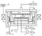
図1は、本発明を、半導体ウエハのエッチングを行う平行平板型のプラズマエッチング装置に適用した実施の形態の構成の概略を模式的に示すものであり、同図において、符号1は、材質が例えばアルミニウム等からなり、内部を気密に閉塞可能に構成された円筒状の真空チャンバを示している。
【0019】
この真空チャンバ1内には、半導体ウエハWを載置するための載置台2が設けられており、この載置台2は下部電極を兼ねている。また、真空チャンバ1内の天井部には、上部電極を構成するシャワーヘッド3が設けられており、これらの載置台2とシャワーヘッド3によって、一対の平行平板電極が構成されるようになっている。
【0020】
上記シャワーヘッド3には、ガス拡散用の空隙4が設けられるとともに、このガス拡散用の空隙4の下側に位置するように多数の細孔5が設けられている。そして、処理ガス供給系6から供給された所定の処理ガスを、ガス拡散用の空隙4内で拡散させ、細孔5から半導体ウエハWに向けてシャワー状に供給するよう構成されている。本実施形態では、このシャワーヘッド3は、接地電位とされているが、シャワーヘッド3に高周波電源が接続され、載置台2とシャワーヘッド3の双方に高周波電力が印加される構成としても良い。
【0021】
一方、載置台2には、2つの整合器7,8を介して2つの高周波電源9,10が接続されており、載置台2に、2種類の所定周波数(例えば、100MHzと3.2MHz)の高周波電力を重畳して供給可能とされている。なお、載置台2に高周波電力を供給する高周波電源を1台のみとして、1種類の周波数の高周波電力のみを供給する構成としても良い。
【0022】
また、載置台2の半導体ウエハWの載置面には、半導体ウエハWを吸着保持するための静電チャック11が設けられている。この静電チャック11は、絶縁層11a内に静電チャック用電極11bを配設した構成とされており、静電チャック用電極11bには、直流電源12が接続されている。さらに、載置台2の上面には、半導体ウエハWの周囲を囲むように、フォーカスリング13が設けられている。
【0023】
真空チャンバ1の底部には、排気ポート14が設けられ、この排気ポート14には、真空ポンプ等から構成された排気系15が接続されている。
【0024】
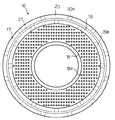
また、載置台2の周囲には、環状に形成された排気リング16が設けられている。この排気リング16は、図2にも示すように、下方に向かって略垂直に形成された側壁部17と、この側壁部17の下端から内側に向かって垂直方向に延在する底部18とを具備している。
【0025】
上記側壁部17は、図3に示すように、同心状に、所定間隔を設けて配置された内側円筒状部材19と、外側円筒状部材20とから構成されている。内側円筒状部材19には、円周方向に沿って所定間隔を設けて、排気路を構成する縦長の矩形状の複数の開口19aが設けられている。また、図3,4に示すように、外側円筒状部材20にも、同様に排気路を構成する縦長の矩形状の複数の開口20aが設けられており、開口19aと開口20aとは、円周方向に所定間隔(図4に示す距離C)ずらして配置されている。
【0026】
そして、図4に矢印で示すように、内側円筒状部材19の開口19aを通り、この後、内側円筒状部材19と外側円筒状部材20との間に形成された間隙21内を通り、しかる後、外側円筒状部材20の開口20aを通ってガスが排気されるように排気路が形成されている。
【0027】
図4に示す、寸法A〜D、すなわち間隙21の幅A、開口19aの幅B、開口19aと開口20aとのずれ幅C、内側円筒状部材19の厚さDについては、以下の条件、
C/A>1
B>2A
B/D>1
を満たすよう構成されている。
【0028】
すなわち、排気リング16においては、間隙21の部分においてプラズマをトラップする構造となっており、このため、間隙21の幅Aは比較的狭く設定され、開口19aと開口20aとのずれ幅Cはプラズマをトラップするのに充分な距離を有するよう設定されている。
【0029】
また、開口19aの幅Bについては、ここでプラズマをトラップする構造ではないため、充分な開口面積をとり、充分なコンダクタンスを確保することができるように広く設定され、同様な理由から、内側円筒状部材19の厚さDについては、薄く設定されている。なお、外側円筒状部材20の厚さ及び開口20aについても、同様な設定とされている。
【0030】
なお、図4は、排気リング16の構成を模式的に示すものであり、実際の寸法を示すものではない。実際の寸法については、例えば、間隙21の幅Aを1mmとした場合、開口19aの幅Bは2mmより大きくなり、例えば数ミリ程度とされる。また、開口19aと開口20aとのずれ幅C、内側円筒状部材19の厚さDについても、上記した条件から逆算される大きさで、かつ、加工のし易さ等を考慮して設定される。
【0031】
また、側壁部17の上下方向の長さについても、上記の開口19a及び開口20aの開口面積を充分にとれ、充分なコンダクタンスを確保することができる長さとされている。
【0032】
上記のように、排気リング16の側壁部17に排気路を形成することにより、側壁部17の上下方向の長さ長くすることによって、開口面積を充分にとれ、充分なコンダクタンスを確保することができる。また、このようにして、開口面積を広くしても、排気リング16の直径は一定であるので、真空チャンバ1の直径は大きくする必要がなく、装置のフットプリントが増大することがない。
【0033】
また、上記のように、側壁部17の排気路を、開口19aと、間隙21と、開口20aとから構成することによって、プラズマのリークを防止する機能を充分確保しつつ、開口面積を充分にとれ、充分なコンダクタンスを確保することができる。
【0034】
すなわち、開口19aの開口面積を大きくすることによって、図4に示した矢印のようなガスの流れとともに、プラズマ中の電子は、この開口19aを通り抜けるが、電子の進行方向には、外側円筒状部材20があるため、さらに、電子が間隙21内を通り抜け、開口20aから外部に導出される可能性は極めて低くなり、プラズマが開口20aの外までリークする可能性は極めて低くなるので、充分なコンダクタンスを確保できるように開口面積を大きくしても、プラズマのリークを防止する機能を充分確保することができるようになっている。
【0035】
さらに、本実施形態では、排気リング16の底部18にも、多数の円孔からなる開口18aが形成され、これらの開口18aによって排気路が形成されている。このように、底部18にも排気路を形成することにより、コンダクタンスをさらに高めることができる。
【0036】
上記のような排気リング16の底部18の排気路は、円孔等の開口でなく、側壁部17に設けた上述した構成の排気路とすることもできる。しかしながら、底部18は、プラズマが形成される領域からかなり離れているので、プラズマのリークを防止する機能については、さほど考慮する必要がなく、このため円孔等からなる開口とすることができる。また、側壁部17に設けた排気路によって充分なコンダクタンスを確保することができる場合は、底部18の排気路は設けなくとも良い。
【0037】
上記の排気リング16の材質は、導電性のものであれば、どのようなものでも良く、例えば、ステンレス、表面にアルマイト被膜や溶射膜が形成されたアルミニウム等を使用することができる。このように、導電性の材料から構成された排気リング16は、電気的に接地電位に接続されている。
【0038】
そして、上記のように構成された排気リング16を介して、排気系15により、排気ポート14から真空排気することによって、真空チャンバ1内を所定の真空雰囲気に設定できるよう構成されている。
【0039】
また、真空チャンバ1の周囲には、磁場形成機構22が設けられており、真空チャンバ1内の処理空間に、所望の磁場を形成できるようになっている。この磁場形成機構22には、回転機構23が設けられており、真空チャンバ1の周囲で磁場形成機構22を回転させることにより、真空チャンバ1内の磁場を回転可能に構成されている。
【0040】
次に、このように構成されたプラズマエッチング装置におけるエッチング処理について説明する。
【0041】
まず、図示しない搬入・搬出口に設けられた図示しないゲートバルブを開放し、搬送機構等により半導体ウエハWを真空チャンバ1内に搬入し、載置台2上に載置する。載置台2上に載置された半導体ウエハWは、この後、静電チャック11の静電チャック用電極11bに、直流電源12から所定の直流電圧を印加することにより、吸着保持される。
【0042】
次に、搬送機構を真空チャンバ1外へ退避させた後、ゲートバルブを閉じ、真空系15の真空ポンプ等により真空チャンバ1内を排気し、真空チャンバ1内が所定の真空度になった後、真空チャンバ1内に、ガス拡散用の空隙4、細孔5を介して、処理ガス供給系6から所定のエッチング処理用の処理ガスを、例えば100〜1000sccmの流量で導入し、真空チャンバ1内を所定の圧力、例えば1.33〜133Pa(10〜1000mTorr)程度に保持する。
【0043】
この状態で、高周波電源9,10から載置台2に、所定周波数(例えば、100MHzと3.2MHz)の高周波電力を供給する。
【0044】
上記のように、載置台2に高周波電力が印加されることにより、シャワーヘッド3と載置台2との間の処理空間には高周波電界が形成される。また、処理空間には、磁場形成機構22よる所定の磁場が形成される。これにより処理空間に供給された処理ガスから所定のプラズマが発生し、そのプラズマにより半導体ウエハW上の所定の膜がエッチングされる。
【0045】
この際、前述したとおり、排気リング16のコンダクタンスが高いので、真空チャンバ内から効率的に真空排気を行うことができ、大型で高性能な真空ポンプ等を使用しなくとも、容易に高真空度に設定することができる。また、排気リング16において確実にプラズマのリークを防止することができるため、安定したプラズマによって、所望のエッチング処理を高精度で実施することができる。
【0046】
そして、所定のエッチング処理が実行されると、高周波電源9,10からの高周波電力の供給を停止し、エッチング処理を停止して、上述した手順とは逆の手順で、半導体ウエハWを真空チャンバ1外に搬出する。
【0047】
なお、上記実施の形態においては、本発明を半導体ウエハのエッチングを行うプラズマエッチング装置に適用した場合について説明したが、本発明はかかる場合に限定されるものではない。例えば、半導体ウエハ以外の基板を処理するものであっても良く、エッチング以外の処理、例えばCVD等の成膜処理装置にも適用することができる。
【0048】
【発明の効果】
以上説明したとおり、本発明のプラズマ処理装置によれば、高いガスコンダクタンス能力を備え、製造コストの上昇を招くことなく、広範なプロセスに対応することができるとともに、プラズマのリークを防止する機能が高く、安定したプラズマにより良好なプラズマ処理を行うことができる。
【図面の簡単な説明】
【図1】本発明の一実施形態に係るプラズマ処理装置の全体概略構成を示す図。
【図2】図1のプラズマ処理装置の要部概略構成を示す図。
【図3】図1のプラズマ処理装置の要部概略構成を示す図。
【図4】図1のプラズマ処理装置の要部概略構成を示す図。
【符号の説明】
W……半導体ウエハ、1……真空チャンバ、2……載置台、3……シャワーヘッド、9,10……高周波電源、14……排気ポート、15……排気系、16……排気リング、17……側壁部、18……底部、18a……開口、19……内側円筒状部材、19a……開口、20……外側円筒状部材、20a……開口、21……間隙。[0001]
TECHNICAL FIELD OF THE INVENTION
The present invention relates to a plasma processing apparatus for performing a predetermined plasma process such as an etching process or a film forming process by applying plasma to a substrate to be processed, for example, a semiconductor wafer or a glass substrate for a liquid crystal display device.
[0002]
[Prior art]
Conventionally, in the field of manufacturing semiconductor devices, a plasma is generated in a vacuum chamber, and this plasma is applied to a substrate to be processed, for example, a semiconductor wafer or a glass substrate for a liquid crystal display device. A plasma processing apparatus that performs an etching process, a film forming process, and the like is used.
[0003]
In such a plasma processing apparatus, for example, in a so-called parallel-plate type plasma processing apparatus, a mounting table for mounting a semiconductor wafer or the like is provided in a vacuum chamber, and a vacuum chamber of the vacuum chamber is opposed to the mounting table. A shower head is provided on the ceiling, and the mounting table and the shower head form a pair of parallel plate electrodes.
[0004]
Then, a predetermined processing gas is introduced into the vacuum chamber from the shower head, and the processing chamber is evacuated from the bottom of the vacuum chamber to form a processing gas atmosphere having a predetermined degree of vacuum. By supplying high frequency power of a predetermined frequency to the head, plasma of a processing gas is generated, and the plasma is applied to the semiconductor wafer, thereby performing processing such as etching of the semiconductor wafer.
[0005]
In the plasma processing apparatus as described above, the mounting table is evacuated evenly from the periphery of the mounting table to form a uniform flow of the processing gas around the semiconductor wafer and to prevent the plasma from leaking from the processing space. There is known a device provided with an exhaust ring which is formed in an annular plate shape and has a large number of through-holes and a slit-shaped exhaust passage formed therearound (see, for example, Patent Document 1).
[0006]
As described above, the exhaust ring has the function of preventing plasma leakage from the processing space in the vacuum chamber. However, in order to improve the function of preventing such plasma leakage, it is necessary to use an exhaust ring. It is necessary to reduce the opening area of the exhaust path or lengthen the exhaust path to make it difficult for electrons to pass through the exhaust path. When a plasma leak occurs, the plasma becomes unstable, and it becomes difficult to perform a predetermined plasma process on a semiconductor wafer or the like. Therefore, it is necessary to reduce the possibility of occurrence of plasma leak as much as possible.
[0007]
However, if the function of preventing the plasma leakage of the exhaust ring is improved as described above, it becomes impossible to obtain a sufficient conductance for the gas. For this reason, there is a problem that the process that can be performed is limited because the vacuum evacuation performance is reduced. On the other hand, if an attempt is made to secure a high evacuation capacity in order to avoid such a problem, a large-sized, high-performance vacuum pump is required, and there is a problem that the manufacturing cost of the apparatus increases.
[0008]
[Patent Document 1]
Japanese Utility Model Laid-Open No. 5-8937 (FIG. 1-3).
[0009]
[Problems to be solved by the invention]
As described above, in the conventional plasma processing apparatus, when the function of preventing the leakage of the plasma of the exhaust ring is improved, the conductance to the gas is reduced, and it is difficult to achieve both. For this reason, there has been a problem that a desired plasma process cannot be performed due to occurrence of a plasma leak, and a process that can be performed is limited due to a decrease in conductance to gas.
[0010]
The present invention has been made in view of such a conventional situation, has a high gas conductance capability, can cope with a wide range of processes without increasing manufacturing costs, and prevents plasma leakage. It is an object of the present invention to provide a plasma processing apparatus capable of performing good plasma processing with high function and stable plasma.
[0011]
[Means for Solving the Problems]
That is, the plasma processing apparatus according to
[0012]
The plasma processing apparatus according to claim 2 is the plasma processing apparatus according to
[0013]
The plasma processing apparatus according to claim 3 is the plasma processing apparatus according to claim 2, wherein the opening provided in the inner cylindrical member and the opening provided in the outer cylindrical member are vertically long. It is characterized by being formed in a rectangular shape and being provided at a predetermined interval along the circumferential direction.
[0014]
The plasma processing apparatus according to
[0015]
A plasma processing apparatus according to a fifth aspect is the plasma processing apparatus according to any one of the first to fourth aspects, wherein the exhaust path is provided at the bottom of the exhaust ring.
[0016]
7. The plasma processing apparatus according to
[0017]
BEST MODE FOR CARRYING OUT THE INVENTION
Hereinafter, embodiments of the present invention will be described with reference to the accompanying drawings.
[0018]
FIG. 1 schematically shows an outline of the configuration of an embodiment in which the present invention is applied to a parallel plate type plasma etching apparatus for etching a semiconductor wafer. In FIG. This shows a cylindrical vacuum chamber made of, for example, aluminum or the like and configured so that the inside can be hermetically closed.
[0019]
A mounting table 2 on which the semiconductor wafer W is mounted is provided in the
[0020]
The shower head 3 is provided with a
[0021]
On the other hand, two high-
[0022]
An
[0023]
An
[0024]
A ring-shaped
[0025]
As shown in FIG. 3, the
[0026]
Then, as shown by an arrow in FIG. 4, it passes through the
[0027]
The dimensions A to D, ie, the width A of the
C / A> 1
B> 2A
B / D> 1
It is configured to satisfy.
[0028]
That is, the
[0029]
In addition, the width B of the
[0030]
FIG. 4 schematically shows the configuration of the
[0031]
In addition, the vertical length of the
[0032]
As described above, by forming the exhaust path in the
[0033]
Further, as described above, by forming the exhaust passage of the
[0034]
That is, by increasing the opening area of the
[0035]
Further, in the present embodiment,
[0036]
The exhaust path at the bottom 18 of the
[0037]
The material of the
[0038]
Then, the interior of the
[0039]
Further, a magnetic
[0040]
Next, an etching process in the plasma etching apparatus configured as described above will be described.
[0041]
First, a gate valve (not shown) provided at a loading / unloading port (not shown) is opened, and the semiconductor wafer W is loaded into the
[0042]
Next, after the transfer mechanism is retracted out of the
[0043]
In this state, high frequency power of a predetermined frequency (for example, 100 MHz and 3.2 MHz) is supplied from the high
[0044]
As described above, by applying the high-frequency power to the mounting table 2, a high-frequency electric field is formed in the processing space between the shower head 3 and the mounting table 2. A predetermined magnetic field is formed in the processing space by the magnetic
[0045]
At this time, as described above, since the conductance of the
[0046]
When the predetermined etching process is performed, the supply of the high-frequency power from the high-
[0047]
In the above embodiment, the case where the present invention is applied to a plasma etching apparatus for etching a semiconductor wafer has been described, but the present invention is not limited to such a case. For example, a substrate other than a semiconductor wafer may be processed, and the present invention can be applied to a process other than etching, for example, a film forming apparatus such as CVD.
[0048]
【The invention's effect】
As described above, according to the plasma processing apparatus of the present invention, it has a high gas conductance capability, can cope with a wide range of processes without increasing production costs, and has a function of preventing plasma leakage. Good plasma treatment can be performed with high and stable plasma.
[Brief description of the drawings]
FIG. 1 is a diagram showing an overall schematic configuration of a plasma processing apparatus according to an embodiment of the present invention.
FIG. 2 is a diagram showing a schematic configuration of a main part of the plasma processing apparatus of FIG. 1;
FIG. 3 is a diagram showing a schematic configuration of a main part of the plasma processing apparatus of FIG. 1;
FIG. 4 is a diagram showing a schematic configuration of a main part of the plasma processing apparatus of FIG. 1;
[Explanation of symbols]
W ... Semiconductor wafer, 1 ... Vacuum chamber, 2 ... Placement table, 3 ... Shower head, 9,10 ... High frequency power supply, 14 ... Exhaust port, 15 ... Exhaust system, 16 ... Exhaust ring, 17 ... side wall part, 18 ... bottom part, 18a ... opening, 19 ... inner cylindrical member, 19a ... opening, 20 ... outer cylindrical member, 20a ... opening, 21 ... gap.
Claims (6)
Translated fromJapanese前記真空チャンバ内に配置され、前記被処理基板が載置される載置台と、
前記真空チャンバ内に、前記被処理基板に所定の処理を施すためのプラズマを発生させるプラズマ発生機構と、
前記載置台の周囲を囲むように配置され、排気路が形成された排気リングと、前記排気路を介して前記真空チャンバ内を真空排気する真空排気機構とを具備したプラズマ処理装置であって、
前記排気リングは、前記載置台の載置面に対して略垂直に形成された側壁部と、この側壁部の下端から内側に向かって延在する底部とを有し、少なくとも前記側壁部に、前記排気路が形成されていることを特徴とするプラズマ処理装置。A vacuum chamber containing a substrate to be processed,
A mounting table that is disposed in the vacuum chamber and on which the substrate to be processed is mounted,
In the vacuum chamber, a plasma generation mechanism that generates plasma for performing a predetermined process on the substrate to be processed,
An plasma processing apparatus comprising: an exhaust ring arranged to surround the mounting table and an exhaust path formed therein; and a vacuum exhaust mechanism configured to evacuate the vacuum chamber through the exhaust path.
The exhaust ring has a side wall formed substantially perpendicular to the mounting surface of the mounting table, and a bottom extending inward from a lower end of the side wall, and at least the side wall includes A plasma processing apparatus, wherein the exhaust path is formed.
前記排気リングの前記側壁部は、同心状に所定間隔を設けて配置された内側円筒状部材と外側円筒状部材とから構成され、前記内側円筒状部材に設けられた開口と、前記外側円筒状部材に設けられた開口とが、ずらして配置されていることを特徴とするプラズマ処理装置。The plasma processing apparatus according to claim 1,
The side wall portion of the exhaust ring includes an inner cylindrical member and an outer cylindrical member that are concentrically arranged at a predetermined interval, and an opening provided in the inner cylindrical member, and the outer cylindrical member. A plasma processing apparatus, wherein an opening provided in a member is displaced.
前記内側円筒状部材に設けられた前記開口と、前記外側円筒状部材に設けられた前記開口は、縦長の矩形状に形成され、円周方向に沿って所定間隔で複数設けられていることを特徴とするプラズマ処理装置。The plasma processing apparatus according to claim 2,
The opening provided in the inner cylindrical member and the opening provided in the outer cylindrical member are formed in a vertically long rectangular shape, and a plurality of openings are provided at predetermined intervals along a circumferential direction. Characteristic plasma processing apparatus.
前記内側円筒状部材に設けられた前記開口と、前記内側円筒状部材と前記外側円筒状部材との間に形成された間隙と、前記外側円筒状部材に設けられた前記開口と、から前記排気路が形成されていることを特徴とするプラズマ処理装置。The plasma processing apparatus according to claim 3,
The exhaust provided from the opening provided in the inner cylindrical member, a gap formed between the inner cylindrical member and the outer cylindrical member, and the opening provided in the outer cylindrical member. A plasma processing apparatus, wherein a path is formed.
さらに前記排気リングの前記底部に前記排気路が設けられていることを特徴とするプラズマ処理装置。The plasma processing apparatus according to claim 1, wherein
Further, the exhaust path is provided at the bottom of the exhaust ring.
前記真空チャンバ内に配置され、前記被処理基板が載置される載置台と、
前記真空チャンバ内に、前記被処理基板に所定の処理を施すためのプラズマを発生させるプラズマ発生機構と、
前記載置台の周囲を囲むように配置され、排気路が形成された排気リングと、前記排気リングの下方から、前記排気路を介して前記真空チャンバ内を真空排気する真空排気機構とを具備したプラズマ処理装置であって、
前記排気リングは、
第1の開口を有する第1の部材と、
前記第1の部材と間隙を設けて配置され前記第1の開口とはずれた位置に第2の開口を有する第2の部材とを具備し、
前記第1の開口から前記間隙内に入り、前記間隙内を通って前記第2の開口から導出されるよう前記排気路が形成され、前記間隙内で前記プラズマがトラップされるよう構成されていることを特徴とするプラズマ処理装置。A vacuum chamber containing a substrate to be processed,
A mounting table that is disposed in the vacuum chamber and on which the substrate to be processed is mounted,
In the vacuum chamber, a plasma generation mechanism that generates plasma for performing a predetermined process on the substrate to be processed,
An exhaust ring arranged to surround the mounting table and having an exhaust path formed therein, and a vacuum exhaust mechanism configured to evacuate the inside of the vacuum chamber through the exhaust path from below the exhaust ring. A plasma processing apparatus,
The exhaust ring,
A first member having a first opening;
A second member having a second opening disposed at a position deviated from the first opening and provided with a gap with the first member;
The exhaust path is formed so as to enter the gap from the first opening, pass through the gap, and be led out of the second opening, and is configured to trap the plasma in the gap. A plasma processing apparatus characterized by the above-mentioned.
Priority Applications (4)
| Application Number | Priority Date | Filing Date | Title |
|---|---|---|---|
| JP2003121214AJP4286576B2 (en) | 2003-04-25 | 2003-04-25 | Plasma processing equipment |
| US10/830,355US20040261712A1 (en) | 2003-04-25 | 2004-04-23 | Plasma processing apparatus |
| US12/405,432US20090255631A1 (en) | 2003-04-25 | 2009-03-17 | Plasma Processing Apparatus and the Upper Electrode Unit |
| US12/894,803US8083891B2 (en) | 2003-04-25 | 2010-09-30 | Plasma processing apparatus and the upper electrode unit |
Applications Claiming Priority (1)
| Application Number | Priority Date | Filing Date | Title |
|---|---|---|---|
| JP2003121214AJP4286576B2 (en) | 2003-04-25 | 2003-04-25 | Plasma processing equipment |
Publications (2)
| Publication Number | Publication Date |
|---|---|
| JP2004327767Atrue JP2004327767A (en) | 2004-11-18 |
| JP4286576B2 JP4286576B2 (en) | 2009-07-01 |
Family
ID=33499853
Family Applications (1)
| Application Number | Title | Priority Date | Filing Date |
|---|---|---|---|
| JP2003121214AExpired - LifetimeJP4286576B2 (en) | 2003-04-25 | 2003-04-25 | Plasma processing equipment |
Country Status (1)
| Country | Link |
|---|---|
| JP (1) | JP4286576B2 (en) |
Cited By (16)
| Publication number | Priority date | Publication date | Assignee | Title |
|---|---|---|---|---|
| JP2008205327A (en)* | 2007-02-22 | 2008-09-04 | Hitachi Kokusai Electric Inc | Substrate processing equipment |
| JP2009129942A (en)* | 2007-11-20 | 2009-06-11 | Utec:Kk | Plasma processing equipment |
| JP2010016021A (en)* | 2008-07-01 | 2010-01-21 | Tokyo Electron Ltd | Plasma processing apparatus |
| JP2012197246A (en)* | 2011-03-22 | 2012-10-18 | Air Water Inc | Method for causing protein to be of low molecular weight |
| JP2013503495A (en)* | 2009-08-31 | 2013-01-31 | ラム リサーチ コーポレーション | Local plasma confinement and pressure control arrangement and method |
| JP2013506301A (en)* | 2009-09-28 | 2013-02-21 | ラム リサーチ コーポレーション | Integrated confinement ring device and method |
| WO2015194397A1 (en)* | 2014-06-19 | 2015-12-23 | 東京エレクトロン株式会社 | Plasma processing device |
| JP2016127260A (en)* | 2014-12-26 | 2016-07-11 | 東京エレクトロン株式会社 | Substrate processing equipment |
| JP2016162997A (en)* | 2015-03-05 | 2016-09-05 | 東京エレクトロン株式会社 | Plasma processing apparatus |
| KR101737014B1 (en) | 2010-05-25 | 2017-05-17 | 도쿄엘렉트론가부시키가이샤 | Plasma processing apparatus |
| WO2017104442A1 (en)* | 2015-12-16 | 2017-06-22 | 東京エレクトロン株式会社 | Plasma treatment device |
| JP2020188194A (en)* | 2019-05-16 | 2020-11-19 | 東京エレクトロン株式会社 | Plasma processing apparatus |
| CN112216586A (en)* | 2019-07-12 | 2021-01-12 | 中微半导体设备(上海)股份有限公司 | Double-station processor for realizing uniform exhaust and plasma processing equipment |
| CN113990732A (en)* | 2017-06-23 | 2022-01-28 | 东京毅力科创株式会社 | Plasma processing apparatus |
| KR20220100524A (en) | 2021-01-08 | 2022-07-15 | 도쿄엘렉트론가부시키가이샤 | Exhaust ring assembly and plasma processing apparatus |
| JP2023152365A (en)* | 2022-04-04 | 2023-10-17 | 東京エレクトロン株式会社 | Plasma processing apparatus |
- 2003
- 2003-04-25JPJP2003121214Apatent/JP4286576B2/ennot_activeExpired - Lifetime
Cited By (28)
| Publication number | Priority date | Publication date | Assignee | Title |
|---|---|---|---|---|
| JP2008205327A (en)* | 2007-02-22 | 2008-09-04 | Hitachi Kokusai Electric Inc | Substrate processing equipment |
| JP2009129942A (en)* | 2007-11-20 | 2009-06-11 | Utec:Kk | Plasma processing equipment |
| JP2010016021A (en)* | 2008-07-01 | 2010-01-21 | Tokyo Electron Ltd | Plasma processing apparatus |
| JP2013503495A (en)* | 2009-08-31 | 2013-01-31 | ラム リサーチ コーポレーション | Local plasma confinement and pressure control arrangement and method |
| JP2013503494A (en)* | 2009-08-31 | 2013-01-31 | ラム リサーチ コーポレーション | Multi-peripheral ring configuration for implementing plasma confinement |
| JP2013506301A (en)* | 2009-09-28 | 2013-02-21 | ラム リサーチ コーポレーション | Integrated confinement ring device and method |
| KR101737014B1 (en) | 2010-05-25 | 2017-05-17 | 도쿄엘렉트론가부시키가이샤 | Plasma processing apparatus |
| JP2012197246A (en)* | 2011-03-22 | 2012-10-18 | Air Water Inc | Method for causing protein to be of low molecular weight |
| WO2015194397A1 (en)* | 2014-06-19 | 2015-12-23 | 東京エレクトロン株式会社 | Plasma processing device |
| JP2016021548A (en)* | 2014-06-19 | 2016-02-04 | 東京エレクトロン株式会社 | Plasma processing device |
| CN108878324A (en)* | 2014-12-26 | 2018-11-23 | 东京毅力科创株式会社 | Substrate processing apparatus |
| CN108878324B (en)* | 2014-12-26 | 2022-04-12 | 东京毅力科创株式会社 | Substrate processing apparatus |
| JP2019212923A (en)* | 2014-12-26 | 2019-12-12 | 東京エレクトロン株式会社 | Substrate processing apparatus |
| JP2016127260A (en)* | 2014-12-26 | 2016-07-11 | 東京エレクトロン株式会社 | Substrate processing equipment |
| JP2016162997A (en)* | 2015-03-05 | 2016-09-05 | 東京エレクトロン株式会社 | Plasma processing apparatus |
| WO2017104442A1 (en)* | 2015-12-16 | 2017-06-22 | 東京エレクトロン株式会社 | Plasma treatment device |
| JP2017112217A (en)* | 2015-12-16 | 2017-06-22 | 東京エレクトロン株式会社 | Plasma processing equipment |
| CN113990732A (en)* | 2017-06-23 | 2022-01-28 | 东京毅力科创株式会社 | Plasma processing apparatus |
| JP7232705B2 (en) | 2019-05-16 | 2023-03-03 | 東京エレクトロン株式会社 | Plasma processing equipment |
| JP2020188194A (en)* | 2019-05-16 | 2020-11-19 | 東京エレクトロン株式会社 | Plasma processing apparatus |
| TWI833017B (en)* | 2019-05-16 | 2024-02-21 | 日商東京威力科創股份有限公司 | Plasma treatment device |
| CN112216586B (en)* | 2019-07-12 | 2023-03-10 | 中微半导体设备(上海)股份有限公司 | Double-station processor for realizing uniform exhaust and plasma processing equipment |
| CN112216586A (en)* | 2019-07-12 | 2021-01-12 | 中微半导体设备(上海)股份有限公司 | Double-station processor for realizing uniform exhaust and plasma processing equipment |
| JP2022107392A (en)* | 2021-01-08 | 2022-07-21 | 東京エレクトロン株式会社 | Exhaust ring assembly and plasma processing equipment |
| KR20220100524A (en) | 2021-01-08 | 2022-07-15 | 도쿄엘렉트론가부시키가이샤 | Exhaust ring assembly and plasma processing apparatus |
| JP7586598B2 (en) | 2021-01-08 | 2024-11-19 | 東京エレクトロン株式会社 | Exhaust ring assembly and plasma processing apparatus |
| JP2023152365A (en)* | 2022-04-04 | 2023-10-17 | 東京エレクトロン株式会社 | Plasma processing apparatus |
| JP7633205B2 (en) | 2022-04-04 | 2025-02-19 | 東京エレクトロン株式会社 | Plasma Processing Equipment |
Also Published As
| Publication number | Publication date |
|---|---|
| JP4286576B2 (en) | 2009-07-01 |
Similar Documents
| Publication | Publication Date | Title |
|---|---|---|
| KR0151769B1 (en) | Plasma etching equipment | |
| US8152925B2 (en) | Baffle plate and substrate processing apparatus | |
| JP4255747B2 (en) | Plasma processing apparatus and plasma processing method | |
| US8236106B2 (en) | Shower head and substrate processing apparatus | |
| CN101689492B (en) | Apparatus and method for processing edge region of substrate | |
| CN1217388C (en) | Plasma treatment device and exhaust ring | |
| JP4141234B2 (en) | Plasma processing equipment | |
| JP4286576B2 (en) | Plasma processing equipment | |
| CN101740298B (en) | Plasma processing apparatus and constituent part thereof | |
| JP5702968B2 (en) | Plasma processing apparatus and plasma control method | |
| JPH0955374A (en) | Plasma treatment apparatus | |
| JP2001077088A (en) | Plasma processing device | |
| JP2016506592A (en) | Capacitively coupled plasma device with uniform plasma density | |
| JP2009200184A (en) | Plasma processing apparatus, and baffle plate of plasma processing apparatus | |
| JP2009239014A (en) | Electrode structure and substrate processing device | |
| JP5432629B2 (en) | Baffle plate and plasma processing apparatus | |
| JPH05114583A (en) | Dry etching equipment | |
| CN100570818C (en) | Plasma processing apparatus | |
| CN205529029U (en) | Diffusion of gases device, process chamber room and semiconductor processing equipment | |
| JP3940467B2 (en) | Reactive ion etching apparatus and method | |
| TW202008459A (en) | Plasma processing device | |
| JP4357849B2 (en) | Plasma processing equipment | |
| JPH08148295A (en) | Plasma treatment apparatus | |
| KR100725614B1 (en) | Plasma processing apparatus | |
| JP4087674B2 (en) | Semiconductor manufacturing equipment |
Legal Events
| Date | Code | Title | Description |
|---|---|---|---|
| A621 | Written request for application examination | Free format text:JAPANESE INTERMEDIATE CODE: A621 Effective date:20060322 | |
| A977 | Report on retrieval | Free format text:JAPANESE INTERMEDIATE CODE: A971007 Effective date:20080623 | |
| A131 | Notification of reasons for refusal | Free format text:JAPANESE INTERMEDIATE CODE: A131 Effective date:20080701 | |
| A521 | Written amendment | Free format text:JAPANESE INTERMEDIATE CODE: A523 Effective date:20080819 | |
| TRDD | Decision of grant or rejection written | ||
| A01 | Written decision to grant a patent or to grant a registration (utility model) | Free format text:JAPANESE INTERMEDIATE CODE: A01 Effective date:20090324 | |
| A01 | Written decision to grant a patent or to grant a registration (utility model) | Free format text:JAPANESE INTERMEDIATE CODE: A01 | |
| A61 | First payment of annual fees (during grant procedure) | Free format text:JAPANESE INTERMEDIATE CODE: A61 Effective date:20090325 | |
| FPAY | Renewal fee payment (event date is renewal date of database) | Free format text:PAYMENT UNTIL: 20120403 Year of fee payment:3 | |
| R150 | Certificate of patent or registration of utility model | Free format text:JAPANESE INTERMEDIATE CODE: R150 | |
| FPAY | Renewal fee payment (event date is renewal date of database) | Free format text:PAYMENT UNTIL: 20150403 Year of fee payment:6 | |
| R250 | Receipt of annual fees | Free format text:JAPANESE INTERMEDIATE CODE: R250 | |
| R250 | Receipt of annual fees | Free format text:JAPANESE INTERMEDIATE CODE: R250 |