JP2004281863A - Nitride semiconductor device and method of manufacturing the same - Google Patents
Nitride semiconductor device and method of manufacturing the sameDownload PDFInfo
- Publication number
- JP2004281863A JP2004281863AJP2003073311AJP2003073311AJP2004281863AJP 2004281863 AJP2004281863 AJP 2004281863AJP 2003073311 AJP2003073311 AJP 2003073311AJP 2003073311 AJP2003073311 AJP 2003073311AJP 2004281863 AJP2004281863 AJP 2004281863A
- Authority
- JP
- Japan
- Prior art keywords
- layer
- nitride semiconductor
- electrode
- type
- bonding
- Prior art date
- Legal status (The legal status is an assumption and is not a legal conclusion. Google has not performed a legal analysis and makes no representation as to the accuracy of the status listed.)
- Granted
Links
Images


Landscapes
- Led Devices (AREA)
- Electrodes Of Semiconductors (AREA)
- Semiconductor Lasers (AREA)
Abstract
Translated fromJapaneseDescription
Translated fromJapanese【0001】
【発明の属する技術分野】
本発明は、発光ダイオード素子(LED)、レーザダイオード素子(LD)等の発光素子、太陽電池、光センサ等の受光素子、あるいはトランジスタ、パワーデバイス等の電子デバイスに用いられる窒化物半導体(InxAlyGa1−x−yN、0≦x、0≦y、x+y≦1)を用いた窒化物半導体素子及びその製造方法に関する。
【0002】
【従来の技術】
サファイアは、そのエピタキシャル成長工程の高温アンモニア雰囲気中における安定性の為、高効率の窒化物半導体の発光素子を成長させる為の基板として望ましいものであることは実証されている。具体的にはサファイア基板上に成長させた窒化物半導体素子は高輝度青色LED、純緑色LEDやLD(レーザーダイオード)に利用されており、その用途はフルカラーディスプレイや信号表示機、イメージスキャナー、光ディスク用光源等大容量の情報を記憶するDVD等のメディアや通信用の光源、又は印刷機器等である。さらに電界効果トランジスタ(FET)のような電子デバイスへの応用も期待されている。
【0003】
窒化物半導体は有望な半導体材料でありながら、バルク単結晶の製造が難しい。したがって、現状ではサファイア、SiC等の異種基板の上に有機金属気相成長法(MOCVD)を利用してGaNを成長させるヘテロエピタキシ技術が汎用されている。特にサファイア基板を用いる場合はサファイア基板上に600℃程度の低温でAlGaNを緩衝層として形成後、その上に窒化物半導体層を成長させる方法が使用されている。これにより、窒化物半導体層の結晶性向上が実現された。
【0004】
しかしながら、サファイアは熱伝導率が悪い絶縁体であり、これにより素子は限定された構造となってしまう。例えば、GaAsやGaPのような導電体基板であれば、電極を半導体装置の上面に1つ、また底面にはもう1つの電極を設けることができるが、サファイア上に成長させた発光素子は上面(同一面)に2つの電極を設けることになる。そのため、サファイア等の絶縁体基板を用いると、導電体基板に比べて同一基板面積における有効発光面積を狭めてしまう。さらに、絶縁体基板を用いた場合、同一φのウェハーから取れる素子(チップ)数が少ないことになる。
【0005】
また、サファイア等の絶縁体基板を用いた窒化物半導体素子はフェイスアップ型やフェイスダウン型があるが、これらは同一面に両電極を有するため、電流密度が局部的に高くなり素子(チップ)が発熱する。また、電極に対するワイヤーボンディング工程においてpn両電極にそれぞれワイヤーが必要なためチップサイズが大きくなりチップの収率が落ちる。更にサファイアは硬度が高く、六方晶の結晶構造である。そのため、サファイアを成長基板として使われた場合はサファイア基板をスクライブによりチップ分離する必要があり、他の基板に比べて製造工程を増加しなければならない。
【0006】
これに対し、p電極とn電極とを対向配置した構造を有する素子が提案されている。例えば、特許文献2には、n型のGaN基板裏面には、Ti/Alからなるn電極を形成させ、p型のGaNからなるp型コンタクト層表面には、Ni/Auからなるp電極を形成させる窒化物半導体素子が記載されている。また、特許文献3には、サファイア基板上に窒化ガリウム層を積層した窒化物半導体結晶において、サファイア基板とGaNバッファー層とを研削除去し、露出したn型GaNにn電極を形成し、p型電極、n型電極を対向した両端面に形成する半導体発光デバイスチップが記載されている。p電極とn電極とを対向配置することにより、電流分布を均一化して素子の発熱を抑制できることが期待できる。
【0007】
このp電極とn電極とを対向配置した素子のn電極には、Ti/Al電極を用いることが特許文献2に記載されている。このTi/Al電極は、例えば、特許文献3に、n型窒化ガリウム系化合物半導体層とオーミック接触が得られる電極として、チタンとアルミニウムとの合金よりなるか、またはチタンとアルミニウムとが積層された多層膜からなる電極と記載の通り、同一面にp電極とn電極が形成された素子におけるn電極としては代表的なものである。その他代表的なn電極としては、W/Al電極などがある。
【0008】
【特許文献1】
特開平7−45867号
【特許文献2】
特開2000−340892号
【特許文献3】
特開平11−238913号
【0009】
【発明が解決しようとする課題】
しかしながら、p電極とn電極とを対向配置した構造を有する素子のn電極に上記のTi/Al電極を用いても、接触抵抗が大きく良好なオーミック特性が得られず、対向配置した構造を有する素子に期待される特性が十分得られないという問題があった。
【0010】
そこで、本発明は上記問題を解決し、p電極とn電極とが対向配置された構造を有し、良好なオーミック特性が得られるn電極を備えた窒化物半導体素子及びその製造方法を提供することを目的とした。
【0011】
【課題を解決するための手段】
上記課題を解決するため、本発明の窒化物半導体素子は、窒化物半導体からなる積層体の一方の主面にp電極を形成する一方、他方の主面にn電極を形成し、両電極を対向配置してなる窒化物半導体素子であって、上記の他方の主面がn型窒化物半導体層の(000−1)面であり、上記n電極が、該(000−1)面に接しn型不純物を含む合金層を有することを特徴とする。
【0012】
本発明によれば、n型不純物を含む合金層を有するn電極を、その合金層がn型窒化物半導体層の(000−1)面に接するように形成することにより、従来のTi/Al電極では困難であった、(000−1)面と良好なオーミック接触を有するn電極を得ることができる。この理由については明らかではないが、以下の理由が考えられる。
ウルツ鉱型の結晶構造を持つGaNは、c軸方向に非対称で、Ga面(0001)(以下、+c面と呼ぶ。)とN面(000−1)(以下、−c面と呼ぶ。)の二つの極性を有し、−c面の表面にはN原子が配列している。従来のn電極、例えばTi/Al電極は+c面上に形成されているのに対し、本発明のn電極は−c面上に形成されている。合金層のn型不純物は、−c面の露出したN原子のダングリングボンドと結合し安定な、例えば、SiN等に変化する。n型不純物は元々窒化物半導体の結晶格子内に取り込まれ易いものであり、結晶格子を壊さない程度に表面のN原子と反応することができる。これにより、GaN層表面近傍(数原子層)がGaN層の層内より高キャリア濃度となり、接触抵抗が低減され、オーミック特性が向上すると考えられる。
本発明の素子は、両電極を対向配置した素子において、接触抵抗を小さくすることができるので、電極面積を小さくすることができ、これにより素子をより小型化することができる。また、接触抵抗が小さくなるので、電流分布が均一化され、素子の発熱を抑制することができ、また発光素子の場合、発光層全体に電流が流れるようになり、より均一かつ高強度に発光させることができる。また、電極が対向配置されているので、p電極とn電極との短絡を防止できることは言うまでもない。
【0013】
また、本発明の素子は、n型窒化物半導体層に含まれるn型不純物に、上記合金層に含まれるn型不純物と同じものを用いることができる。これにより、良好なオーミック接触を得ることができる。
【0014】
また、本発明の素子は、n型不純物にSi又はGeを用いることができる。さらに、合金層を構成する金属には、Al、Ag、Ti、Mo、Nb、Ta、Hf、Pt及びWからなる群から選択された少なくとも1種の金属を用いることができる。
【0015】
また、本発明の素子は、上記積層体が、p電極に接して形成された接合層により接合された導電性基板を有する積層体を用いることができる。導電性基板を有しているので素子の放熱性を向上させることができる。
【0016】
本発明の素子は、例えば、以下の製造方法により作製することができる。すなわち、対向する二つの主面を有する導電性基板の一方の主面上に、p電極、複数の窒化物半導体層からなる積層体、そしてn電極が積層されてなる窒化物半導体素子の製造方法であって、対向する二つの主面を有する絶縁性成長用基板の一方の主面上に、少なくとも、n型窒化物半導体層と、活性層と、p型窒化物半導体層と、を成長させて接合用積層体を形成し、上記p型窒化物半導体層の上に1層以上の金属層から成る第1の接合層を設ける一方、上記導電性基板の一方の主面上に1層以上の金属層から成る第2の接合層を設け、第1の接合層と第2の接合層とを対向させ、上記接合用積層体と上記導電性基板とを加熱圧接して接合し、上記接合用積層体の絶縁性成長用基板を除去して、n型窒化物半導体層を露出せしめ、n型不純物を含み上記露出させたn型窒化物半導体層に接する合金層を有するn電極を形成することを特徴とする。
【0017】
また、本発明の製造方法では、第1の接合層と第2の接合層が、それぞれ第1の共晶形成層と第2の共晶形成層を有し、接合時には、第1及び第2の共晶形成層を構成する金属を互いに拡散させて共晶を形成することができる。
【0018】
また、本発明の製造方法では、絶縁性成長用基板の一方の主面に接して、GaeAl1−eN(0<e≦1)から成るバッファ層と、アンドープのGaN及びn型不純物をドープしたGaNのいずれかから成る高温成長層と、を含む下地層を設けることができる。
【0019】
また、特に380nm以下の紫外領域の窒化物半導体素子においては、上記成長用基板の一方の主面に接して、GaeAl1−eN(0<e≦1)から成るバッファ層と、アンドープのGaN及びn型不純物をドープしたGaNのいずれかから成る高温成長層と、を含む下地層を設けることができる。下地層はその上に成長させる窒化物半導体の結晶性を向上させる効果を有する。さらに、アンドープのGaNまたはn型不純物をドープしたGaNのいずれかから成る高温成長層は、この層を成長させることで、その上に成長させる窒化物半導体層の結晶性を大きく向上させることができる。結晶性の良い窒化物半導体素子を得るためには、成長用基板、さらにはバッファ層の上に高温でGaN層を成長させることが必要となる。この層を成長させずに活性層等を成長させても結晶性が非常に悪く、窒化物半導体発光素子などにおいては、発光出力が非常に弱く、実用的でない。
【0020】
このように、GaNからなる高温成長層を設けることで、結晶性の良い窒化物半導体素子を得ることができるが、下地層としてGaNを含む場合、紫外領域ではGaNの自己吸収により、活性層からの光の一部がこのGaN層で吸収されてしまい、発光出力が低下してしまう。本発明においては、導電性基板を接合した後、成長用基板と下地層のGaNとを除去するようにしたので、素子を構成する窒化物半導体の結晶性を良好に維持しながら、自己吸収を抑制することが可能となる。
【0021】
また、本発明の製造方法では、絶縁性成長用基板を除去後、バッファ層及び高温成長層を除去することができる。
【0022】
また、本発明の製造方法では、上記の除去する工程において、成長用基板の他方の主面の全面に電磁波を照射して成長用基板と下地層とを除去することができる。
【0023】
また、本発明の製造方法によると、窒化物半導体素子の表面の少なくとも一部に、蛍光物質を含有するコーティング層を形成することができる。また、本発明の発光素子は、発光素子からの光を吸収し、その光と異なる波長の光を発光する蛍光物質を含有するコーティング層を発光素子の表面の少なくとも一部に形成してなることができる。
【0024】
本発明の素子、特に発光素子において、導電性基板と接合させて形成された窒化物半導体素子に、活性層のAlaInbGa1−a−bN(0≦a≦1、0≦b≦1、a+b≦1)からの光の一部もしくは全部を吸収して異なる波長の光を発光する蛍光物質が含有されたコーティング層を形成することで、様々な波長の光を発光することができる。特にYAGを含有させることで、白色光を発光することができ、照明用光源など用途も格段に広がる。
【0025】
また、光の一部もしくは全部を吸収して異なる波長の光を発光する蛍光物質について、可視光を吸収して異なる光を発する材料は限られており、材料の選択性に問題がある。しかしながら、紫外光を吸収して異なる光を発する材料は非常に多く、様々な用途に応じてその材料を選択することができる。材料が選択できる要因の一つとしては、紫外光で吸収する蛍光物質は光の変換効率が可視光の変換効率と比べて高いということである。特に白色光においては、演色性の高い白色光を得るなど、可能性はさらに広がる。本発明は、紫外領域で発光する窒化物半導体素子において、自己吸収の少ない窒化物半導体発光素子が得られ、さらに蛍光物質をコーティングすることで、非常に変換効率の高い白色の発光素子を得ることができる。
【0026】
【発明の実施の形態】
以下、図面を参照して本発明の実施の形態について説明する。
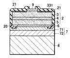
図1は、本発明に係る窒化物半導体素子の構造の一例を示す模式断面図である。素子は、導電性基板8上に、接合層7、p電極6、窒化物半導体から成る積層体2、そしてn電極9が順次積層され、p電極6とn電極9とが対向するように配置され、p電極6とn電極9の露出面以外にそれぞれp側保護膜20とn側保護膜21が形成された構造を有している。ここで、積層体2は、p電極6側から、p型窒化物半導体層5、活性層4、そして露出面にディンブル331を有するn型窒化物半導体層3が順次積層された構造を有している。なお、接合層7は、導電性基板8と積層体2とを接合する役割を果たすものであり、第1の接合層71と第2の接合層72とが一体化して構成されている。
【0027】
より詳しくは、n型窒化物半導体層3の表面は、露出した−c面を有しており、n電極9は−c面に接しn型不純物を含む合金層(不図示)を有している。ここで、n型不純物には、窒化物半導体に用いられる公知の物質を用いることができ、例えば、C、Si、Ge、Se、Sを挙げることができる。なかでもSiを用いることで、表面近傍に高キャリア濃度のGaN層ができるので好ましい。
【0028】
また、合金層を形成する金属は、n型不純物と合金を形成する金属であって、例えば、Al、Ag、Ti、Mo、Nb、Ta、Hf、Pt及びWから成る群から選択された少なくとも1種の金属を用いることができる。好ましい合金層の組成は、W−Al−Si、W−Si、より好ましくはW−Siであり、これらを用いることでSiを含んだ合金を形成しやすい。さらに、WxSi1−xの場合、0.3≦x<1であることが好ましい。xが0.3より小さいとn電極が剥がれやすくなるからである。
【0029】
なお、n電極は上記合金層にさらに1以上の金属層を積層した多層膜とすることが好ましく、例えば、上記合金層にさらにPt/Au、W/Au、Ti/Au、Ni/Auなどの金属多層膜を形成することが好ましい。上記合金層が、Alを含む場合はAlが拡散しやすいので、Alの拡散を防止する層としてTiなどの拡散バリア層をこの金属多層膜層の前記合金層の最も近くに含める。最も好ましくは、合金層を含んだ構成として、W−Si/Pt/Auである。n電極は、合金層あるいは合金形成層に1以上の金属層を蒸着法あるいはスパッタリング法により形成して多層膜とした後、アニールすることにより作製することができる。また、n電極の厚さは、0.1〜1.5μmが好ましい。
【0030】
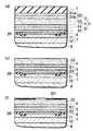
以下、本発明に係る窒化物半導体発光素子の製造方法について説明する。図2から4は、本発明に係る窒化物半導体発光素子の製造工程の一例を示す模式断面図である。成長用基板1の表面に、バッファ層31aと高温成長層31bとから成る下地層32を形成する(図2(a))。次いで、下地層32上にn型クラッド層33を積層してn型窒化物半導体層3を形成し、活性層4、そしてp型クラッド層51とp型コンタクト層52とから成るp型窒化物半導体層5を順次積層する(図2(a))。
【0031】
次に、p型コンタクト層52の上にp電極6を形成する(図2(b))。ここで、p型コンタクト層52の上にp電極6を形成した後、オーミック接触を得るためのアニール処理を行う。さらに、p電極6の露出面以外を覆うように絶縁性のp側保護膜20を形成する。
【0032】
次に、p電極6の上に1層以上の金属層から成る第1の接合層71を形成する(図2(c))。一方、導電性基板8の表面に1層以上の金属層から成る第2の接合層72を形成する(図2(c))。
【0033】
次に、導電性基板8を、第1の接合層71と第2の接合層72とが対向するように成長用基板1の上に積層し、加熱圧接して接合する(図3(d))。ここで、第1の接合層71と第2の接合層72とは接合時に一体化して接合層7を形成する。
【0034】
次に、導電性基板8と接合した成長用基板1を研磨器に設置し、成長用基板1のラッピングを行い、成長用基板1と下地層32を除去して、n型クラッド層33を露出させる(図3(e))。そして、n型クラッド層33の表面を、例えば、ウエットエッチングして、−c面を露出させる。
【0035】
次に、光の取出し効率を向上させるため、n型クラッド層33の露出面を所定パターンのレジストでマスクし、RIEによりエッチングしてn型クラッド層33の表面に凹凸面からなるディンブル331を形成する(図4(f))。なお、この工程は省略することもできる。
【0036】
次に、n型クラッド層33の露出面に所定パターンのSiO2マスクを形成し、素子分離用の分離溝10を形成する(図4(g))。
【0037】
次に、n型クラッド層33上に、n型不純物と、そのn型不純物と合金を形成する金属を含む多層膜を形成し、アニールしてn電極9を形成し、さらにn電極9の露出面以外を覆うように絶縁性のn側保護膜21を形成する(図4(h))。そして、ダイシングにより素子をチップ状に分離する(図4(i))。
【0038】
本発明の方法において、成長用基板には、C面、R面及びA面のいずれかを主面とするサファイヤ、スピネル(MgAl2O4のような絶縁性基板)、そして窒化物半導体と格子整合する酸化物基板等を挙げることができるが、サファイヤやスピネルが好ましい。さらに、成長用基板は、オフアングルしたものを用いることが好ましい。この場合ステップ状にオフアングルしたものを用いることにより、窒化ガリウムから成る下地層の結晶性を向上させることができる。
【0039】
本発明の窒化物半導体発光素子に用いる成長用基板は、凹凸形状を有するディンプルを成長表面に有することが好ましい。凹凸形状を有するディンプルの成長用基板に成長することで、結晶欠陥の少ない窒化物半導体のファセット成長によって、窒化物半導体層を成長させることができ好ましい。ディンプルは具体的には、少なくとも凹部の段差が5nm以上とし、特に凹部および凸部に平面が存在することで、活性層が平滑になり易いので好ましい。活性層が凹凸を有すると、発光特性における歩留が悪くなる。
【0040】
また、成長用基板上に窒化物半導体層を積層する場合、下地層上にELOG(Epitaxially Lateral Overgrowth)成長させることにより結晶性の向上した窒化物半導体を得ることもできる。具体的には、成長用基板上に下地層を成長させ、その下地層上にストライプ状のマスクを複数形成し、マスクの開口部から窒化物半導体を選択成長させ、横方向の成長を伴った成長により成膜された窒化物半導体層(横方向成長層)を形成する。この横方向成長層は貫通転位が低減されているので、横方向成長層の上に形成する窒化物半導体の結晶性を向上させることができる。
【0041】
成長用基板としては、成長用基板となる材料の主面をオフアングルさせた基板、さらにステップ状にオフアングルさせた基板を用いるほうが好ましい。オフアングルさせた基板を用いると、表面の3次元成長が見られず、ステップ成長があらわれ表面が平坦になり易い。さらに、ステップ状にオフアングルされているサファイヤ基板のステップに沿う方向(段差方向)が、サファイヤのA面に対して垂直に形成されていると、窒化物半導体のステップ面がレーザの共振器方向と一致し、レーザ光が表面粗さにより乱反射されることが少なくなり好ましい。
【0042】
また、導電性基板は導電性を有する基板材料であれば良く、例えば、Si、SiC等の半導体から成る半導体基板、又は、金属単体基板、又は相互に非固溶あるいは固溶限界の小さい2種以上の金属の複合体から成る金属基板を用いることができるが、金属基板を用いることが好ましい。金属基板は、半導体基板に比べ機械的特性が優れており、弾性変形、さらには塑性変形し易く、割れにくいからである。さらに、金属基板には、Ag,Cu,Au,Pt等の高導電性金属から選択された1種以上の金属と、W,Mo,Cr,Ni等の高硬度の金属から選択された1種以上の金属と、から成るものを用いることができる。さらに、金属基板としては、Cu−WあるいはCu−Moの複合体を用いることが好ましい。熱伝導率の高いCuを有し放熱性が優れているからである。さらに、Cu−Wの複合体の場合、Cuの含有率xが0<x≦30重量%、Cu−Moの複合体の場合、Cuの含有率xが0<x≦50重量%であることが好ましい。また、Cu−ダイヤ等の金属とセラミックスの複合体などを用いることができる。なお、導電性基板の厚さは、放熱性を高めるため50〜500μmが好ましい。
【0043】
また、第1の接合層は、少なくとも、p型窒化物半導体層とオーミック接触し、高い反射率を有するp電極をp型窒化物半導体層に接して有することが好ましい。p電極には、Rh、Ag、Ni/Au、Ni/Au/Rh及びRh/Irのいずれか、より好ましくは、Rh/Irを用いることができる。ここで、p電極は、n型窒化物半導体層に比べ抵抗率の高いp型窒化物半導体層上に形成するため、p型窒化物半導体層のほぼ全面に形成することが好ましい。なお、p電極の厚さは、0.05〜0.5μmが好ましい。
【0044】
また、第1の接合層のp電極を形成したp型窒化物半導体層の露出面に絶縁性の保護膜を形成することが好ましい。この保護膜の材料には、SiO2、Al2O3、ZrO2、TiO2、Ta2O5、Nb2O5、MgF2、SiN等が挙げられ、これらを単層または多層で形成する。多層で形成する場合は、屈折率が相対的に(低屈折率/高屈折率)となるように窒化物半導体層側から繰り返して形成するとよい。これら単層膜、多層膜の膜厚を調整して反射させる。活性層からの光が反射するような膜厚に調整しない場合は、その保護膜の上にAl、Ag、Rh等の高反射率の金属膜を形成してもよい。これらの構成とすることで、光の取り出し効率を向上させることができる。
【0045】
また、第1の接合層のp電極の上に第1の共晶形成層を設けるとともに、第2の接合層に、導電性基板の主面の上に第2の共晶形成層を設けることが好ましい。第1及び第2の共晶形成層は、接合時に互いに拡散して共晶を形成する層であり、それぞれ、Au、Sn、Pd、In等の金属から成る。第1及び第2の共晶形成層の組合せは、Au−Sn、Sn−Pd、又はIn−Pdが好ましい。さらに好ましくは、第1の共晶形成層にSnを、そして第2の共晶形成層にAuを用いる組合せである。
【0046】
また、第1の接合層の第1の共晶形成層とp電極との間に、p電極側から密着層とバリア層を設けることが好ましい。密着層はp電極との間に高い密着性を確保する層であり、Ti、Ni、W及びMoのいずれかの金属が好ましい。また、バリア層は、第1の共晶形成層を構成する金属が密着層へ拡散するのを防止する層であり、PtあるいはWが好ましい。また、第1の共晶形成層の金属が密着層へ拡散するのをさらに防止するため、バリア層と第1の共晶形成層との間に、0.3μm程度の厚さのAu膜を形成しても良い。なお、第2の共晶層と導電性基板との間に、上記の密着層とバリア層及びAu膜を設けることが好ましい。
【0047】
また、接合用積層体と導電性基板とを加熱圧接する際の温度は、150℃以上500℃以下、好ましくは150℃以上350℃以下が好ましい。150℃以上とすることにより、共晶形成層の金属の拡散が促進され均一な密度分布の共晶が形成され、接合用積層体と導電性基板との密着性を向上させることができる。500℃より大きいと、共晶形成層の金属がバリア層、さらには密着層まで拡散して、良好な密着性が得られないからである。
【0048】
また、導電性基板を接合後に成長用基板を除去するには、研磨、エッチング、電磁波照射、あるいはこれらの方法を組合せた方法を用いることができる。電磁波照射は、電磁波に例えばレーザを用い、導電性基板を接合後、成長用基板の下地層の形成されていない面の全面にレーザを照射して、下地層を分解させることにより成長用基板と下地層とを除去することができる。さらに、成長用基板と下地層とを除去した後、露出した窒化物半導体層の表面をCMP処理して所望の膜を露出させる。これにより、ダメージ層の除去や、窒化物半導体層の厚み及び表面粗さの調整を行うことができる。
【0049】
なお、電磁波照射には、以下の方法を用いることもできる。すなわち、成長用基板上に窒化物半導体からなる下地層を形成し、次いで、その下地層を部分的に成長用基板までエッチングして凹凸を形成した後、凹凸を有する下地層上にELOG成長させて横方向成長層を形成する。次いで、横方向成長層の上にn型窒化物半導体層、活性層、p型窒化物半導体層を順次形成した後、p型窒化物半導体層の上に導電性基板を接合する。次いで、成長用基板の下地層の形成されていない面の全面にレーザを照射して、下地層を分解させることにより成長用基板と下地層とを除去することができる。この方法によれば、電磁波照射時に窒化物半導体の分解により発生するN2ガスが上記の凹凸と横方向成長層との間に形成された空隙に広がり、ガス圧による成長用基板の割れを防止し、さらにその割れに起因する下地層のえぐれ傷を防止して、面状態及び結晶性の良好な窒化物半導体基板を得ることができる。また、研磨による方法に比べ、作業工程を簡略化することができるので、歩留まりが向上するという効果も得られる。
【0050】
また、成長用基板を除去した後、光の取出し効率を向上させるため、n型窒化物半導体層の露出面をRIEにより凹凸(ディンプル加工)を形成しても良い。その凹凸の断面形状は、メサ型あるいは逆メサ型、そして、平面形状は島状、格子状、矩形状、円状あるいは多角形状とすることができる。
【0051】
また、n電極以外の露出面を覆うように、SiO2、Al2O3、ZrO2、TiO2、Si3N4、MgF2、Nb2O5、Ta2O5等の絶縁性の保護膜を形成する。この層は単層または多層で、反射しないような無反射コート(ARコート)膜とする。
【0052】
なお、p電極とn電極は、窒化物半導体素子の一方の主面にp電極が、他方の主面にn電極が形成されている限り、大きさや形状は特に限定されない。好ましくは、両電極が窒化物半導体層の積層方向から見て、互いに重ならないように対向配置されている限り、大きさや形状は特に限定されない。これにより、フェイスダウン構造の場合、発光した光を、n電極により遮られることなく効率良く取出すことができる。例えば、p電極をp型窒化物半導体層の概ね全面に形成した場合、n電極を、n型窒化物半導体層の隅部の2つ又は4つに形成しても良く、格子状に全面に形成しても良く、さらには、隅部に格子状に形成することもできる。
【0053】
以下、本実施の形態に係る窒化物半導体素子の具体的構成について、図2から4を参照して説明する。
本発明において、n型窒化物半導体層、活性層、及びp型窒化物半導体層は、いずれも窒化物半導体からなり、好ましくはAlxInyGa1−x−yN(0≦x、0≦y、x+y≦1)からなる。またいずれの層もAlxInyGa1−x−yN(0≦x、0≦y、x+y<1)、すなわちGaを含む窒化物半導体を少なくとも1層有する。n型窒化物半導体層およびp型窒化物半導体層は、複数の層から成り、クラッド層として機能する層を少なくとも有する。またn型窒化物半導体層においては、基板との接合面に、基板上に窒化物半導体層をエピタキシャル成長させるための、バッファ層を有する。また活性層は、単一量子井戸構造、多重量子井戸構造のいずれでも良く、好ましくは、井戸層と障壁層とが繰り返し積層されてなる多重量子井戸構造とする。本発明の窒化物半導体発光素子をレーザ素子として形成する場合は、さらに活性層とクラッド層との間に光ガイド層も設ける。
また380nm以下で発光する窒化物半導体発光素子を得る場合、次のように、下地層からp型コンタクト層までを形成することで、発光効率のよい発光素子を得ることができる。
【0054】
(下地層)
下地層32は、少なくとも1層以上の窒化物半導体で構成することができるが、成長用基板1上に低温成長させたバッファ層31aと、そのバッファ層31a上に高温成長させた高温成長層31bとで構成することが好ましい。
【0055】
バッファ層31aとしては、GaiAl1−iN(0<i≦1)からなる窒化物半導体であり、好ましくはAlの割合が小さいもの、より好ましくはGaNを用いることによりバッファ層上に成長させる窒化物半導体の結晶性が向上する。バッファ層の膜厚は、好ましくは0.002〜0.5μm、より好ましくは0.005〜0.2μm、さらに好ましくは0.01〜0.02μmである。バッファ層の成長温度は、好ましくは200〜900℃、より好ましくは400〜800℃である。
【0056】
高温成長層31bとしては、好ましくはアンドープのGaN又はn型不純物をドープしたGaNを用いることができる。高温成長層の膜厚は、500Å以上、より好ましくは5μm以上、さらに好ましくは10μm以上である。また、高温成長層の成長温度は、900〜1100℃、好ましくは1050℃以上である。
【0057】
(n型クラッド層)
n型クラッド層33としては、活性層4のバンドギャップエネルギーより大きくなる組成であり、活性層4へのキャリア閉じ込めが可能であれば特に限定されないが、AljGa1−jN(0<j<0.3)が好ましい。ここで、さらに好ましくは、0.1<j<0.2である。n型クラッド層の膜厚は特に限定されるものではないが、好ましくは0.01〜0.1μm、より好ましくは0.03〜0.06μmである。また、n型クラッド層のn型不純物濃度は特に限定されるものではないが、好ましくは1×10¹⁷〜1×10²⁰/cm3、より好ましくは1×1018〜1×1019/cm3である。また、本発明においては、導電性基板を接合した後、成長用基板と下地層および高温成長層のGaNとを除去する場合、ある程度の膜厚が必要であり、その場合は1μm〜10μm、より好ましくは1μm〜5μmとする。
【0058】
(活性層)
本発明に用いる活性層4は、少なくとも、AlaInbGa1−a−bN(0≦a≦1、0≦b≦1、a+b≦1)から成る井戸層と、AlcIndGa1−c−dN(0≦c≦1、0≦d≦1、c+d≦1)から成る障壁層と、を含む量子井戸構造を有する。さらに好ましくは、上記井戸層及び障壁層が、それぞれ、AlaInbGa1−a−bN(0<a≦1、0<b≦1、a+b<1)と、AlcIndGa1−c−dN(0<c≦1、0≦d≦1、c+d<1)である。また、活性層における波長は380nm以下であり、具体的には井戸層のバンドギャップエネルギーが波長380nm以下のものである。
【0059】
活性層に用いられる窒化物半導体は、ノンドープ、n型不純物ドープ、p型不純物ドープのいずれでも良いが、好ましくは、ノンドープもしくはアンドープ、又はn型不純物ドープの窒化物半導体を用いることにより発光素子を高出力化することができる。さらに好ましくは、井戸層をアンドープとし、障壁層をn型不純物ドープとすることで、発光素子の出力と発光効率を高めることができる。
【0060】
(p型クラッド層)
p型クラッド層52としては、活性層4のバンドギャップエネルギーより大きくなる組成であり、活性層4へのキャリアの閉じ込めができるものであれば特に限定されないが、AlkGa1−kN(0≦k<1)が用いられ、特にAlkGa1−kN(0<k<0.4)が好ましい。ここで、より好ましくは、0.15<k<0.3である。p型クラッド層の膜厚は特に限定されないが、好ましくは0.01〜0.15μm、より好ましくは0.04〜0.08μmである。p型クラッド層のp型不純物濃度は、1×10¹⁸〜1×10²¹/cm3、1×1019〜5×1020cm3である。p型不純物濃度が上記の範囲にあると、結晶性を低下させることなくバルク抵抗を低下させることができる。
【0061】
(p型コンタクト層)
p型コンタクト層51は、AlfGa1−fN(0≦f<1)が用いられ、特に、AlfGa1−fN(0<f<0.3)で構成することによりオーミック電極6と良好なオーミックコンタクトが可能となる。p型不純物濃度は1×10¹⁷/cm3以上が好ましい。
【0062】
また、p型コンタクト層は、導電性基板側でp型不純物濃度が高く、かつ、Alの混晶比が小さくなる組成勾配を有することが好ましい。この場合、組成勾配は、連続的に組成を変化させても、あるいは、不連続に段階的に組成を変化させても良い。例えば、p型コンタクト層を、p電極と接し、p型不純物濃度が高くAl組成比の低い第1のp型コンタクト層と、p型不純物濃度が低くAl組成比の高い第2のp型コンタクト層とで構成することもできる。第1のp型コンタクト層により良好なオーミック接触が得られ、第2のp型コンタクト層により自己吸収を防止することが可能となる。
【0063】
第1のp型コンタクト層の組成は、AlgGa1−gN(0≦g<0.05)が好ましく、より好ましくはgが、0<g<0.01である。Al組成比が上記の範囲内であれば、p型不純物を高濃度にドープしても不純物の不活性化を防止でき、良好なオーミック接触が得られる。また、第1のp型コンタクト層のp型不純物濃度は、好ましくは1×10¹⁹〜1×10²²/cm3、より好ましくは5×1020〜5×1021/cm3である。また、第1のp型コンタクト層の膜厚は、好ましくは100〜500Å、より好ましくは150〜300Åである。
【0064】
また、第2のp型コンタクト層の組成は、AlhGa1−hN(0≦h<0.1)が好ましく、より好ましくはhが、0.1<h<0.05である。Al組成比が上記の範囲内であれば、自己吸収を防止することが可能となる。また、第2のp型コンタクト層のp型不純物濃度は、好ましくは1×10²⁰/cm3以下、より好ましくは5×1018〜5×1019/cm3である。また、第2のp型コンタクト層の膜厚は、好ましくは400〜1200Å、より好ましくは800〜1200Åである。
以上のような構成とし、成長用基板と下地層、さらには高温成長層のGaNを除去することで、自己吸収のない窒化物半導体発光素子を得ることができる。
【0065】
【実施例】
以下、実施例を用いて本発明をさらに詳細に説明する。
実施例1.
本実施例に用いた窒化物半導体の積層体の構造を図5に示す。n型窒化物半導体層3は、成長基板1に、バッファ層31aと高温成長層31bとから成る下地層32、n型コンタクト層34、n型第1多層膜層35、そしてn型超格子多層膜層36とを順次積層して構成されている。また、p型窒化物半導体層5は、活性層4に、多層膜p型クラッド層51、p型低濃度ドープ層53、そしてp型コンタクト層52とを順次積層して構成されている。以下、この積層体の作製方法及びこの積層体を用いたLED素子の作製方法について、図2〜5を参照して説明する。
【0066】
(成長用基板)
サファイア(C面)よりなる成長用基板1をMOVPEの反応容器内にセットし、水素を流しながら、基板の温度を1050℃まで上昇させ、基板のクリーニングを行った。
【0067】
(下地層)
バッファ層:続いて、温度を510℃まで下げ、キャリアガスに水素、原料ガスにアンモニアとTMG(トリメチルガリウム)とを用い、基板1上にAlGaNよりなるバッファ層31aを約200Åの膜厚で成長させた。なおこの低温で成長させるバッファ層は基板の種類、成長方法等によっては省略できる。
【0068】
高温成長層:バッファ層31a成長後、TMGのみ止めて、温度を1050℃まで上昇させた。1050℃になったら、同じく原料ガスにTMG、アンモニアガスを用い、アンドープGaN層31bを1.5μmの膜厚で成長させた。
【0069】
(n型コンタクト層)
続いて1050℃で、同じく原料ガスにTMG、アンモニアガス、不純物ガスにシランガスを用い、Siを6×10¹⁸/cm3ドープしたGaNよりなるn型コンタクト層34を1.85μmの膜厚で成長させた。
【0070】
(第1多層膜層)
次にシランガスのみを止め、1050℃で、TMG、アンモニアガスを用い、アンドープGaNからなる下層を3000Åの膜厚で成長させ、続いて同温度にてシランガスを追加しSiを6×10¹⁸/cm3ドープしたGaNからなる中間層を300Åの膜厚で成長させ、更に続いてシランガスのみを止め、同温度にてアンドープGaNからなる上層を50Åの膜厚で成長させ、3層からなる総膜厚3350Åの第1多層膜層35を成長させた。
【0071】
(n型超格子多層膜層)
次に、同様の温度で、アンドープGaNよりなる第1の窒化物半導体層を40Å成長させ、次に温度を800℃にして、TMG、TMI、アンモニアを用い、アンドープIn0.02Ga0.98Nよりなる第2の窒化物半導体層を20Å成長させた。そしてこれらの操作を繰り返し、第1+第2の順で交互に10層づつ積層させ、最後にGaNよりなる第1の窒化物半導体層を40Å成長させた超格子構造の多層膜よりなるn型超格子多層膜層36を640Åの膜厚で成長させた。
【0072】
(活性層)
次に、アンドープGaNよりなる障壁層を200Åの膜厚で成長させ、続いて温度を800℃にして、TMG、TMI、アンモニアを用いアンドープIn0.4Ga0.6Nよりなる井戸層を30Åの膜厚で成長させた。そして障壁+井戸+障壁+井戸・・・・+障壁の順で障壁層を5層、井戸層4層交互に積層して、総膜厚1120Åの多重量子井戸構造よりなる活性層4を成長させた。
【0073】
(中濃度ドープの多層膜p型クラッド層)
次に、温度1050℃でTMG、TMA、アンモニア、Cp2Mg(シクロペンタジエニルマグネシウム)を用い、Mgを5×10¹⁹/cm3ドープしたp型Al0.2Ga0.8Nよりなる第1の窒化物半導体層を40Åの膜厚で成長させ、続いて温度を800℃にして、TMG、TMI、アンモニア、Cp2Mgを用いMgを5×1019/cm3ドープしたIn0.03Ga0.97Nよりなる第2の窒化物半導体層を25Åの膜厚で成長させた。そしてこれらの操作を繰り返し、第1+第2の順で交互に5層ずつ積層し、最後に第1の窒化物半導体層を40Åの膜厚で成長させた超格子構造の多層膜よりなるp側多層膜クラッド層51を365Åの膜厚で成長させた。
【0074】
(低濃度ドープのp型低濃度ドープ層)
続いて、1050℃で、TMG、アンモニアを用い、アンドープのGaNよりなるp型低濃度ドープ層53を2000Åの膜厚で成長させた。この低濃度ドープ層は、成長時はアンドープとして成長させるが、中濃度ドープの多層膜p型クラッド層51にドープされているMgが、低濃度ドープ層53を成長する間に拡散し、さらに下記の高濃度ドープのp型コンタクト層52を成長させる際にMgが拡散し、低濃度ドープ層はp型を示す。
この低濃度ドープ層53のMg濃度は、最も濃度が低い部分では、2×10¹⁸/cm3となる。また低濃度ドープ層53のMg濃度の変化は、p型クラッド層51に接している部分ではp型クラッド層51のMg濃度とほぼ同様の値を示すが、p型クラッド層51から離れるに従い徐々に減少し、後で成長させるp型コンタクト層52と接近している付近(p型コンタクト層52を成長させる直前)でのMg濃度がほぼ最低値を示す。
【0075】
(高濃度ドープのp型コンタクト層)
続いて、1050℃で、TMG、アンモニア、Cp2Mgを用い、Mgを1×10²⁰/cm3ドープしたGaNよりなるp型コンタクト層52を1200Åの膜厚で成長させる。
反応終了後、温度を室温まで下げ、さらに窒素雰囲気中、ウェーハを反応容器内において、700℃でアニーリングを行い、p型層をさらに低抵抗化する。
【0076】
(p電極)
アニーリング後、ウェハを反応容器から取出し、p型コンタクト層52の上にRh/Ir/Pt膜を膜厚400Å/500Å/1000Åで形成してp電極6とした。その後、オーミックアニールを600℃で行った後、p電極6以外の露出面に絶縁性のp側保護膜20としてSiO2を膜厚0.3μmで形成した。
【0077】
(第1の接合層)
次に、p電極の上に、第1の接合層71として、Ti/Pt/Au/Sn/Auの多層膜を、膜厚1000Å/1000Å/1000Å/30000Å/1000Åで形成した。ここで、Tiは密着層、Ptはバリア層、Snは第1の共晶形成層、そしてPtとSnの間のAu層は、Snがバリア層へ拡散するのを防止する役割を果たし、最外層のAu層は第2の共晶形成層との密着性を向上させる役割を果たす。この第1の接合層71は、少なくともp電極上に形成され、好ましくは接合用積層体のp電極側の全面に形成する。
【0078】
(第2の接合層)
一方、導電性基板8として、膜厚が200μmで、Cu30%とW70%の複合体から成る金属基板を用い、その金属基板の表面に、第2の接合層72として、Tiから成る密着層、Ptから成るバリア層、そしてAuから成る第2の共晶形成層を、この順で、膜厚1000Å/1000Å/14000Åで形成した。
【0079】
次に、第1の接合層71と第2の接合層72とを対向させた状態で、接合用積層体2と導電性基板8とを、ヒータ温度を250℃でプレス加圧して加熱圧接した。これにより、第1の共晶形成層と第2の共晶形成層の金属を互いに拡散させて共晶を形成させた。
【0080】
(成長用基板の除去)
次に、導電性基板8を接合した接合用積層体2について、サファイヤ基板の下地層側の反対面から、波長248nmのKrFエキシマレーザを用いて、出力600J/cm2で、レーザ光を1mm×50mmの線状にして上記の反対面全面をスキャンしてレーザを照射した。レーザ照射により下地層の窒化物半導体を分解して、サファイヤ基板を除去した。さらに、バッファ層と、アンドープGaN層を、さらにはn型コンタクト層が露出するまで研磨し、露出したn型コンタクト層をKOH及びコロイダルシリカ(K2SiO3)を用いてケミカルポリッシュ研磨して面荒れをなくした。n型コンタクト層は、p型コンタクト層までの膜厚が3μm程度となるまで研磨した。
【0081】
(ディンプル形成)
次に、n型窒化物半導体層の露出面をRIEにより凹凸形状のディンプル331にする。この形状は直径4μm、深さ1μmの円柱状の凹部が規則的に配列されたものとする。
【0082】
(積層体分離)
次に、n型コンタクト層側から、n型コンタクト層からp型コンタクト層までをエッチングして、p側保護膜を露出させ、所望のチップサイズになるように窒化物半導体からなる積層体を分離する。
【0083】
(n電極)
次に、露出したn型コンタクト層上に、W−Si/Pt/Auから成るn電極9を、膜厚200Å/2000Å/6000Åで蒸着してn電極とし、n電極以外のn型コンタクト層の露出面と積層体の側面の全てを覆うようにn側保護膜21として、SiO2をARコートした。ここで、WSi合金の組成は、WxSi1−xである。なお、本実施例では、n電極のサイズを100μm×100μmとした。
【0084】
(素子分離)
その後、導電性基板を100μmまで研磨した後、導電性基板の裏面にp電極用のパッド電極として、Ti/Pt/Auから成る多層膜を1000Å/2000Å/3000Åで成膜した。次に、ダイシングにより素子を分離した。
【0085】
得られたLED素子は、サイズが250μm×250μmであり、順方向電流20mAにおいて、460nmの青色発光を示し、Vfは3.55Vであった。
【0086】
比較例1.
n電極に、W/Al/Ti/Pt/Auからなる多層電極(膜厚100Å/2500Å/1000Å/2000Å/6000Å)を用いた以外は、実施例1と同様の条件で素子を作製した。ここで、Pt/Auはパッド電極であり、TiはAlがPt/Auに拡散するのを防ぐ層として機能しており、従来オーミック電極としてAlを含む合金または多層膜を用いる場合は、Al拡散防止層としてTiなどを形成する必要がある。
【0087】
得られたLED素子は、順方向電流20mAにおいて、460nmの青色発光を示し、Vfは5.19Vであった。
【0088】
比較例2.
高濃度ドープのp型コンタクト層を形成し、700℃でアニーリングを行うまでは実施例1と同様である。
次に高濃度ドープのp型コンタクト層を形成後、p型コンタクト層側から、p型窒化物半導体層と活性層とn型窒化物半導体層の一部までをエッチングし、n型コンタクト層を露出させた。このn型コンタクト層の露出面に、W/Al/Ti/Pt/Auを形成した場合と、W−Si/Pt/Auを形成した場合とを、n電極のオーミック特性について調べたが、W−Si/Pt/Auを用いたことによるオーミック接触の向上は見られなかった。n型窒化物半導体層の(0001)面にn電極を形成する場合は、本発明の効果は見られないことがわかった。
【0089】
実施例2.
n電極9をW−Al−Si/Ti/Pt/Auからなる多層電極とし、膜厚を200Å/1000Å/2000Å/6000Åとした以外は、実施例1と同様にして素子を作製した。得られた素子は実施例1とほぼ同等の特性を示した。
【0090】
実施例3.
(成長用基板)
成長用基板として、サファイヤ(C面)よりなる基板を用い、MOCVD反応容器内において水素雰囲気中、1050℃で表面のクリーニングを行った。
【0091】
(下地層)
バッファ層:続いて、水素雰囲気中、510℃でアンモニアとTMG(トリメチルガリウム)を用い、基板上にGaNよりなるバッファ層を約200Åの膜厚で成長させた。
【0092】
高温成長層:バッファ層成長後、TMGのみを止めて、温度を1050℃まで上昇させ、1050℃になったら、原料ガスにTMG、アンモニアを用い、アンドープGaNよりなる高温成長の窒化物半導体を5μmの膜厚で成長させた。
【0093】
(n型クラッド層)
次に、1050℃でTMG、TMA、アンモニア、シランを用い、Siを5×10¹⁷/cm3ドープしたn型Al0.18Ga0.82Nよりなるn型クラッド層を400Åの膜厚で形成した。
【0094】
(活性層)
次に、温度を800℃にして、原料ガスにTMI(トリメチルインジウム)、TMG、TMAを用い、SiドープのAl0.1Ga0.9Nよりなる障壁層、その上にアンドープのIn0.03Al0.02Ga0.95Nよりなる井戸層を、障壁層▲1▼/井戸層▲1▼/障壁層▲2▼/井戸層▲2▼/障壁層▲3▼の順に積層した。この時、障壁層▲1▼を200Å、障壁層▲2▼と▲3▼を40Å、井戸層▲1▼と▲2▼を70Åの膜厚で形成した。活性層は、総膜厚約420Åの多重量子井戸構造(MQW)となる。
【0095】
(p型クラッド層)
次に、水素雰囲気中、1050℃でTMG、TMA、アンモニア、Cp2Mg(シクロペンタジエニルマグネシウム)を用い、Mgを1×10²⁰/cm3ドープしたAl0.2Ga0.8Nよりなるp型クラッド層を600Åの膜厚で成長させた。
【0096】
(p型コンタクト層)
続いて、p型クラッド層上に、TMG、TMA、アンモニア、Cp2Mgを用いて、Mgを1×10¹⁹/cm3ドープしたAl0.04Ga0.96Nよりなる第2のp型コンタクト層を0.1μmの膜厚で成長させ、その後、ガスの流量を調整してMgを2×1021/cm3ドープしたAl0.01Ga0.99Nよりなる第2のp型コンタクト層を0.02μmの膜厚で成長させた。
【0097】
成長終了後、窒素雰囲中、ウェハを反応容器内において、700℃でアニーリングを行い、p型層をさらに低抵抗化した。
【0098】
(p電極)
アニーリング後、ウェハを反応容器から取出し、p型コンタクト層の上にRh/Ir/Pt膜を膜厚400Å/500Å/1000Åで形成してp電極とした。その後、オーミックアニールを600℃で行った後、p電極以外の露出面に絶縁性のp側保護膜20としてSiO2を膜厚0.3μmで形成した。
【0099】
(第1の接合層)
次に、p電極の上に、第1の接合層71として、Ti/Pt/Au/Sn/Auの多層膜を、膜厚1000Å/1000Å/1000Å/30000Å/1000Åで形成した。ここでで、Tiは密着層、Ptはバリア層、Snは第1の共晶形成層、そしてPtとSnの間のAu層は、Snがバリア層へ拡散するのを防止する役割を果たし、最外層のAu層は第2の共晶形成層との密着性を向上させる役割を果たす。この第1の接合層71は、少なくともp電極上に形成され、好ましくは接合用積層体のp電極側の全面に形成する。
【0100】
(第2の接合層)
一方、導電性基板8として、膜厚が200μmで、Cu30%とW70%の複合体から成る金属基板を用い、その金属基板の表面に、第2の接合層72として、Tiから成る密着層、Ptから成るバリア層、そしてAuから成る第2の共晶形成層を、この順で、膜厚1000Å/1000Å/14000Åで形成した。
【0101】
次に、第1の接合層71と第2の接合層72とを対向させた状態で、接合用積層体2と導電性基板8とを、ヒータ温度を250℃でプレス加圧して加熱圧接した。これにより、第1の共晶形成層と第2の共晶形成層の金属を互いに拡散させて共晶を形成させた。
【0102】
(成長用基板の除去)
次に、導電性基板8を接合した接合用積層体2について、サファイヤ基板の下地層側の反対面から、波長248nmのKrFエキシマレーザを用いて、出力600J/cm2で、レーザ光を1mm×50mmの線状にして上記の反対面全面をスキャンしてレーザを照射した。レーザ照射により下地層の窒化物半導体を分解して、サファイヤ基板を除去した。さらに、バッファ層と、アンドープGaN層を、さらにはn型コンタクト層が露出するまで研磨し、露出したn型コンタクト層をKOH及びコロイダルシリカ(K2SiO3)を用いてケミカルポリッシュ研磨して面荒れをなくした。n型コンタクト層は、p型コンタクト層までの膜厚が3μm程度となるまで研磨した。
【0103】
(ディンプル形成)
次に、n型窒化物半導体層の露出面をRIEにより凹凸形状のディンプル331にする。この形状は直径4μm、深さ1μmの円柱状の凹部が規則的に配列されたものとした。
【0104】
(積層体分離)
次に、n型コンタクト層側から、n型コンタクト層からp型コンタクト層までをエッチングして、p側保護膜を露出させ、所望のチップサイズになるように窒化物半導体からなる積層体を分離した。
【0105】
(n電極)
次に、n型クラッド層上に、W−Si/Pt/Auから成るn電極9を、膜厚200Å/2000Å/6000Åで蒸着してn電極とした。n電極以外のn型コンタクト層露出面と積層体の側面の全てを覆うようにn側保護膜21として、SiO2をARコートした。ここで、WSi合金の組成は、WxSi1−xであった。なお、本実施例では、n電極のサイズを100μm×100μmとした。
【0106】
(素子分離)
その後、導電性基板を100μmまで研磨した後、導電性基板の裏面にp電極用のパッド電極として、Ti/Pt/Auから成る多層膜を1000Å/2000Å/3000Åで成膜した。次に、ダイシングにより素子を分離した。
【0107】
得られたLED素子は、サイズが250μm×250μmであり、373nmの紫外発光を示し、n電極がn型クラッド層と良好なオーミック接触が得られていることが確認された。
【0108】
以上説明したように、本発明のLED素子は、従来のn電極を用いた場合に比べ、Vfが低下し、発光効率を向上させることができた。また、n電極とn型コンタクト層とが良好なオーミック接触となるので、n電極のサイズを小さくすることができ、発光出力の向上も期待できる。
【0109】
次に実施例として窒化物半導体を用いた半導体レーザ素子について、図6を参照して説明するが、本発明の半導体素子は、これに限らず、本発明の技術的思想において、様々な半導体に実施できることは言うまでもない。
【0110】
実施例4.
(下地層)
バッファ層:2インチφ、C面を主面とするサファイアよりなる異種基板を成長用基板としMOVPE反応容器内にセットし温度を500℃にして、トリメチルガリウム(TMG)、アンモニア(NH3)を用い、GaNよりなるバッファ層を200Åの膜厚で成長させた。
【0111】
高温成長層:バッファ層形成後、温度を1050℃にして、TMG、アンモニアを用い、アンドープGaNよりなる窒化物半導体層を4μmの膜厚で成長させた。この層は、素子構造を形成する各層の成長において実質的な下地層(成長用基板)として作用する。下地層としてこの他にELOG(Epitaxially Laterally Overgrowth)成長させた窒化物半導体を用いると結晶性が良好な成長用基板が得られる。ELOG成長層の具体例としては、異種基板上に、窒化物半導体層を成長させ、その表面に窒化物半導体の成長が困難な保護膜を設ける等して形成したマスク領域と、窒化物半導体を成長させる非マスク領域とをストライプ状に設け、その非マスク領域から窒化物半導体を成長させることで、膜厚方向への成長に加えて横方向への成長が成されることにより、マスク領域にも窒化物半導体が成長して成膜させたものや、異種基板上に成長させた窒化物半導体層に開口部を設け、その開口部側面から横方向への成長が成されて成膜されたもの等が挙げられる。
次に、高温成長層の上に、積層体を構成する各層を形成する。
【0112】
(n型コンタクト層)
続いて1050℃で、同じく原料ガスにTMG、アンモニアガス、不純物ガスにシランガスを用い、Siを4.5×10¹⁸/cm3ドープしたGaNよりなるn型コンタクト層を2.25μmの膜厚で成長させた。このn型コンタクト層の膜厚は2〜30μmであればよい。
【0113】
(クラック防止層)
次に、TMG、TMI(トリメチルインジウム)、アンモニアを用い、温度を800℃にしてIn0.06Ga0.94Nよりなるクラック防止層を0.15μmの膜厚で成長させた。なお、このクラック防止層は省略可能である。
【0114】
(n型クラッド層)
次に、温度を1050℃にして、原料ガスにTMA(トリメチルアルミニウム)、TMG及びアンモニアを用い、アンドープのAlGaNよりなるA層を25Åの膜厚で成長させ、続いてTMAを止め、不純物ガスとしてシランガスを用い、Siを5×10¹⁸/cm3ドープしたGaNよりなるB層を25Åの膜厚で成長させた。そしてこの操作をそれぞれ160回繰り返してA層とB層を交互に積層し、総膜厚8000Åの多層膜(超格子構造)よりなるn型クラッド層を成長させた。この時、アンドープAlGaNのAlの混晶比としては、0.05以上0.3以下の範囲であれば、十分にクラッド層として機能する屈折率差を設けることができる。
【0115】
(n型光ガイド層)
次に、同様の温度で原料ガスにTMG及びアンモニアを用い、アンドープのGaNよりなるn型光ガイド層を0.1μmの膜厚で成長させた。この層は、n型不純物をドープさせてもよい。
【0116】
(活性層)
次に、温度を800℃にして、原料にTMI(トリメチルインジウム)、TMG及びアンモニアを用い、不純物ガスとしてシランガスを用い、Siを5×10¹⁸/cm3ドープしたIn0.05Ga0.95Nよりなる障壁層を100Åの膜厚で成長させた。続いてシランガスを止め、アンドープのIn0.1Ga0.9Nよりなる井戸層を50Åの膜厚で成長させる。この操作を3回繰り返し、最後に障壁層を積層させて総膜厚550Åの多重量子井戸構造(MQW)の活性層を成長させた。
【0117】
(p型キャップ層)
次に、同様の温度で、原料ガスにTMA、TMG及びアンモニアを用い、不純物ガスとしてCp2Mg(シクロペンタジエニルマグネシウム)を用い、Mgを1×10¹⁹/cm3ドープしたAlGaNよりなるp型電子閉じ込め層を100Åの膜厚で成長させた。
【0118】
(p型光ガイド層)
次に、温度を1050℃にして、原料ガスにTMG及びアンモニアを用い、アンドープのGaNよりなるp型光ガイド層を750Åの膜厚で成長させた。このp型光ガイド層はアンドープとして成長させるが、Mgをドープさせてもよい。
【0119】
(p型クラッド層)
続いて、1050℃でアンドープAl0.16Ga0.84Nよりなる層を25Åの膜厚で成長させ、続いてTMGを止め、Cp2Mgを用いてMgドープGaNよりなる層を25Åの膜厚で成長させ、総膜厚0.6μmの超格子層よりなるp型クラッド層を成長させた。p型クラッド層は少なくとも一方がAlを含む窒化物半導体層を含み、互いにバンドギャップエネルギーが異なる窒化物半導体層を積層した超格子で作製した場合、不純物はいずれも一方の層に多くドープして、いわゆる変調ドープを行うと結晶性がよくなる傾向にあるが、両方に同じようにドープさせてもよい。
【0120】
(p型コンタクト層)
最後に1050℃でp型クラッド層の上にMgを1×10²⁰/cm3ドープしたp型GaNよりなるp型コンタクト層を150Åの膜厚で成長させた。p型コンタクト層はp型のInxAlyGa1−x−yN(x≦0、y≦0、x+y≦1)で構成することができ、好ましくはMgをドープしたGaNとすればp電極と最も好ましいオーミック接触が得られる。反応終了後、反応容器内において窒素雰囲気中でウエハを700℃でアニーリングして、p型層を更に低抵抗化した。
【0121】
(n型層露出及び共振器面形成)
以上のようにして窒化物半導体を形成した後、ウエハを反応容器から取り出し、最上層のp型コンタクト層の表面にSiO2よりなる保護膜を形成してRIE(反応性イオンエッチング)を用いSiCl4ガスによりエッチングし、共振器面となる活性層端面を露出させてエッチング端面を共振器端面とした。
【0122】
(基板露出)
次に、SiO2をウエハ全面に形成した後、その上にn型コンタクト層の露出面を除いてレジスト膜を形成し、基板が露出するまでエッチングする。共振器面など側面にもレジスト膜が形成されているので、エッチング後には、先に形成させた共振器面などの側面(p型層15と、活性層14と、n型層13の一部と、を含む)と、共振器面と基板との間のn型層との2段になった端面が形成されることになる。
【0123】
(ストライプ状凸部形成)
次に、ストライプ状の導波路領域を形成するために、最上層のp型コンタクト層のほぼ全面にCVD装置により、Si酸化物(主としてSiO2)よりなる保護膜を0.5μmの膜厚で形成した後、保護膜の上に幅3μmのストライプ形状のマスクをかけ、RIE装置によりCF4ガスを用いてSiO2をエッチングし、その後SiCl4により窒化物半導体層をp型ガイド層が露出するまでエッチングし、活性層よりも上にストライプ状の凸部が形成される。
【0124】
(第1の絶縁膜)
SiO2マスクをつけたまま、p型半導体層表面にZrO2よりなる第1の絶縁膜22を形成した。この第1の絶縁膜は後に分割され易いように絶縁膜を形成させない部分を設けてもよい。第1の絶縁膜形成後、バッファード液に浸漬して、ストライプ状凸部の上面に形成したSiO2を溶解除去し、リフトオフ法によりSiO2と共に、p型コンタクト層上(更にはn型コンタクト層上)にあるZrO2を除去する。これにより、ストライプ状凸部の上面は露出され、凸部の側面はZrO2で覆われた構造となる。
【0125】
(p電極)
次に、p型コンタクト層上の凸部最表面にp電極16を形成した。このp電極は、Ni/Auからなる。電極形成後、それぞれを酸素:窒素が1:99の割合の雰囲気中で、600℃でアニーリングすることで、p電極を合金化し、良好なオーミック特性を得る。
【0126】
(第2の絶縁膜)
次に、Si酸化物(主としてSiO2)とTi酸化膜(TiO2)の多層膜からなる第2の絶縁膜23をλ/4nの膜厚で2ペア(4層)の条件で、エッチングされた底面及び側面に形成することでミラーを形成した。このときpパッド電極は露出するようにしておく。
【0127】
(pパッド電極)
次に、第1の絶縁膜を介してストライプ状凸部上面のp電極と電気的に接続する、Ti/Pt/Auからなるpパッド電極24を形成した。
【0128】
(接合層)
次に、pパッド電極の上に第1の接合層171を形成した。本発明の半導体レーザ素子の第1の接合層は、第1の共晶層からなり、各層は、p型半導体層側からSn/Auの順に膜厚30000Å/1000Åで形成した。
他方、導電性基板を用意する。膜厚が200μmでありCu20%、W80%から成る導電性基板の表面に第2の接合層172をTi/Pt/Auの順に膜厚2000Å/3000Å/12000Åで形成した。
次に前記第1の接合層171と、導電性基板の第2の接合層172とを接合させて、両者を貼り合わせた。240℃でプレス圧力をかけた。ここで共晶形成層が形成される。その後、研削によってサファイア基板を除去後、露出したn型コンタクト層をKOH及びコロイダルシリカ(K2SiO3)を用いてケミカルポリッシュ研磨して面荒れを無くした。
次に前記n型コンタクト層上にn電極19をW−Si/Pt/Auの順に膜厚200Å/2000Å/6000Åで形成した。その後、導電性基板を100μmまで研磨した後、導電性基板の裏面にTi/Pt/Auを1000Å/2000Å/3000Åで成膜した後、ダイシングを行って素子を分離した。
【0129】
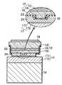
図6は、得られた窒化物半導体レーザ素子の構造を示す模式断面図である。
素子は、導電性基板18上に、接合層17、第1の絶縁膜22を介してp電極16と電気的に接続するpパッド電極24、p電極16、窒化物半導体から成る積層体12、そしてn電極19が順次積層され、p電極16とn電極19とが対向するように配置された構造を有している。さらに、積層体12はそのエッチングされた側面に、ミラーを形成する第2の絶縁膜23を有している。なお、接合層17は、導電性基板18と積層体12とを接合する役割を果たすものであり、第1の接合層171と第2の接合層172とが一体化して構成されている。
【0130】
以上のようにして得られる窒化物半導体レーザ素子は、従来のn電極にTi/Al/Ti/Pt/Auを用いたときと比べてしきい値電圧が低下し、n電極がn型コンタクト層と良好なオーミック接触が得られていることが確認された。
【0131】
【発明の効果】
以上述べたように、本発明の窒化物半導体素子は、p電極とn電極とが対向配置された構造を有し、n型不純物を含む合金層を有するn電極を、その合金層がn型窒化物半導体層の(000−1)面に接するように形成し、n電極が(000−1)面と良好なオーミック接触を得られるようにしたので、素子の小型化が可能で、放熱性に優れ、発光出力の高い素子を提供することが可能となる。
【図面の簡単な説明】
【図1】本発明に係る窒化物半導体素子の構造の一例を示す模式断面図である。
【図2】本発明に係る窒化物半導体素子の製造方法の一例を示す模式断面図(1)である。
【図3】本発明に係る窒化物半導体素子の製造方法の一例を示す模式断面図(2)である。
【図4】本発明に係る窒化物半導体素子の製造方法の一例を示す模式断面図(3)である。
【図5】本発明に係る窒化物半導体素子の製造に用いる窒化物半導体の積層体の構造の一例を示す模式断面図である。
【図6】本発明に係る窒化物半導体レーザ素子の構造の一例を示す模式断面図である。
【符号の説明】
1 成長用基板、2,12 積層体、3,13 n型窒化物半導体層、31aバッファ層、31b 高温成長層、32 下地層、33 n型クラッド層、331 ディンプル、34 n型コンタクト層、35 n型第1多層膜層、36 n型超格子多層膜層、4,14 活性層、5,15 p型窒化物半導体層、51p型クラッド層、52 p型コンタクト層、53 p型低濃度ドープ層、6,16 p電極、7,17 接合層、71,171 第1の接合層、72,172第2の接合層、8,18 導電性基板、9,19 n電極、10 分離溝、20 p側保護膜、21 n側保護膜、22 第1の絶縁膜、23 第2の絶縁膜、24 pパッド電極。[0001]
TECHNICAL FIELD OF THE INVENTION
The present invention relates to a light emitting element such as a light emitting diode element (LED) and a laser diode element (LD), a light receiving element such as a solar cell and an optical sensor, or a nitride semiconductor (In) used for an electronic device such as a transistor and a power device.x Aly Ga1-xy The present invention relates to a nitride semiconductor device using N, 0 ≦ x, 0 ≦ y, x + y ≦ 1) and a method of manufacturing the same.
[0002]
[Prior art]
It has been demonstrated that sapphire is desirable as a substrate for growing a highly efficient nitride semiconductor light emitting device because of its stability in a high temperature ammonia atmosphere in the epitaxial growth step. Specifically, nitride semiconductor elements grown on sapphire substrates are used for high-brightness blue LEDs, pure green LEDs, and LDs (laser diodes), and are used for full-color displays, signal displays, image scanners, optical disks, and the like. Media such as a DVD that stores a large amount of information such as a light source for communication; a light source for communication; or a printing device. Further, application to electronic devices such as a field effect transistor (FET) is also expected.
[0003]
Although a nitride semiconductor is a promising semiconductor material, it is difficult to manufacture a bulk single crystal. Therefore, at present, a heteroepitaxy technique for growing GaN on a heterogeneous substrate such as sapphire or SiC by using metal organic chemical vapor deposition (MOCVD) is widely used. In particular, when a sapphire substrate is used, a method of forming AlGaN as a buffer layer on a sapphire substrate at a low temperature of about 600 ° C. and then growing a nitride semiconductor layer thereon is used. Thereby, the crystallinity of the nitride semiconductor layer was improved.
[0004]
However, sapphire is an insulator having poor thermal conductivity, which results in the device having a limited structure. For example, in the case of a conductive substrate such as GaAs or GaP, one electrode can be provided on the top surface of the semiconductor device and another electrode can be provided on the bottom surface, but the light emitting element grown on sapphire has a top surface. Two electrodes will be provided on the same surface. Therefore, when an insulating substrate such as sapphire is used, the effective light emitting area in the same substrate area is reduced as compared with the conductive substrate. Furthermore, when an insulator substrate is used, the number of elements (chips) that can be obtained from a wafer having the same φ is small.
[0005]
In addition, there are face-up type and face-down type nitride semiconductor devices using an insulating substrate such as sapphire. Since these devices have both electrodes on the same surface, the current density locally increases and the device (chip) Generates heat. Further, in the wire bonding step for the electrodes, since wires are required for both the pn electrodes, the chip size increases and the chip yield decreases. Further, sapphire has a high hardness and a hexagonal crystal structure. Therefore, when sapphire is used as a growth substrate, the sapphire substrate must be separated into chips by scribing, and the number of manufacturing steps must be increased as compared with other substrates.
[0006]
On the other hand, an element having a structure in which a p-electrode and an n-electrode are opposed to each other has been proposed. For example, in
[0007]
[0008]
[Patent Document 1]
JP-A-7-45867
[Patent Document 2]
JP-A-2000-340892
[Patent Document 3]
JP-A-11-238913
[0009]
[Problems to be solved by the invention]
However, even when the above-mentioned Ti / Al electrode is used as the n-electrode of the element having the structure in which the p-electrode and the n-electrode are arranged to face each other, the contact resistance is large and good ohmic characteristics cannot be obtained, so that the element has a structure where the electrodes are opposed to each other. There has been a problem that the characteristics expected of the element cannot be sufficiently obtained.
[0010]
Therefore, the present invention solves the above problem, and provides a nitride semiconductor device having a structure in which a p-electrode and an n-electrode are arranged to face each other and having an n-electrode capable of obtaining good ohmic characteristics, and a method of manufacturing the same. It was aimed at.
[0011]
[Means for Solving the Problems]
In order to solve the above-mentioned problems, a nitride semiconductor device of the present invention has a structure in which a p-electrode is formed on one main surface of a stacked body made of a nitride semiconductor, and an n-electrode is formed on the other main surface. In the nitride semiconductor element arranged to face each other, the other main surface is the (000-1) plane of the n-type nitride semiconductor layer, and the n electrode is in contact with the (000-1) plane. It has an alloy layer containing an n-type impurity.
[0012]
According to the present invention, by forming an n-electrode having an alloy layer containing an n-type impurity such that the alloy layer is in contact with the (000-1) plane of the n-type nitride semiconductor layer, a conventional Ti / Al An n-electrode having good ohmic contact with the (000-1) plane, which was difficult with an electrode, can be obtained. Although the reason for this is not clear, the following may be considered.
GaN having a wurtzite crystal structure is asymmetric in the c-axis direction, and has a Ga plane (0001) (hereinafter, referred to as + c plane) and an N plane (000-1) (hereinafter, referred to as -c plane). N atoms are arranged on the surface of the −c plane. A conventional n-electrode, for example, a Ti / Al electrode is formed on a + c plane, whereas an n-electrode of the present invention is formed on a −c plane. The n-type impurity in the alloy layer is bonded to the dangling bond of the exposed N atom on the −c plane and changes to stable, for example, SiN. The n-type impurity is originally easily taken into the crystal lattice of the nitride semiconductor, and can react with N atoms on the surface to such an extent that the crystal lattice is not broken. Thereby, it is considered that the carrier concentration near the surface of the GaN layer (several atomic layers) becomes higher than that in the GaN layer, the contact resistance is reduced, and the ohmic characteristics are improved.
In the device of the present invention, the contact resistance can be reduced in the device in which both electrodes are arranged to face each other, so that the electrode area can be reduced, and thus the device can be further miniaturized. In addition, since the contact resistance is reduced, the current distribution is made uniform, and the heat generation of the element can be suppressed. In the case of a light emitting element, the current flows through the entire light emitting layer, and the light emission becomes more uniform and high intensity. Can be done. Since the electrodes are arranged to face each other, it goes without saying that a short circuit between the p-electrode and the n-electrode can be prevented.
[0013]
In the device of the present invention, the same n-type impurity contained in the alloy layer can be used as the n-type impurity contained in the n-type nitride semiconductor layer. Thereby, good ohmic contact can be obtained.
[0014]
In the device of the present invention, Si or Ge can be used as the n-type impurity. Furthermore, at least one metal selected from the group consisting of Al, Ag, Ti, Mo, Nb, Ta, Hf, Pt and W can be used as the metal constituting the alloy layer.
[0015]
Further, the element of the present invention can use a laminate in which the above laminate has a conductive substrate joined by a joining layer formed in contact with a p-electrode. Since the device has the conductive substrate, the heat dissipation of the device can be improved.
[0016]
The device of the present invention can be manufactured, for example, by the following manufacturing method. That is, a method of manufacturing a nitride semiconductor device in which a p-electrode, a laminate including a plurality of nitride semiconductor layers, and an n-electrode are laminated on one main surface of a conductive substrate having two opposing main surfaces And growing at least an n-type nitride semiconductor layer, an active layer, and a p-type nitride semiconductor layer on one main surface of an insulating growth substrate having two opposing main surfaces. To form a bonding laminate, and to provide a first bonding layer made of one or more metal layers on the p-type nitride semiconductor layer, and to form one or more layers on one main surface of the conductive substrate. A second bonding layer made of a metal layer is provided, the first bonding layer and the second bonding layer are opposed to each other, and the bonding laminate and the conductive substrate are bonded by heating and pressure bonding. The insulating growth substrate of the stack is removed to expose the n-type nitride semiconductor layer, and the n-type impurity is removed. And forming an n-electrode having an alloy layer in contact with the n-type nitride semiconductor layer formed by the exposed include.
[0017]
Further, in the manufacturing method of the present invention, the first bonding layer and the second bonding layer have a first eutectic forming layer and a second eutectic forming layer, respectively. Can be formed by diffusing the metals constituting the eutectic forming layer.
[0018]
Further, in the manufacturing method of the present invention, Ga in contact with one main surface of the insulating growth substrate is provided.e Al1-e An underlayer including a buffer layer made of N (0 <e ≦ 1) and a high-temperature growth layer made of either undoped GaN or GaN doped with an n-type impurity can be provided.
[0019]
In particular, in a nitride semiconductor device in the ultraviolet region of 380 nm or less, Ga is in contact with one main surface of the growth substrate.e Al1-e An underlayer including a buffer layer made of N (0 <e ≦ 1) and a high-temperature growth layer made of either undoped GaN or GaN doped with an n-type impurity can be provided. The underlayer has the effect of improving the crystallinity of the nitride semiconductor grown thereon. Furthermore, by growing this layer of a high-temperature growth layer made of either undoped GaN or GaN doped with an n-type impurity, the crystallinity of the nitride semiconductor layer grown thereon can be greatly improved. . In order to obtain a nitride semiconductor device having good crystallinity, it is necessary to grow a GaN layer at a high temperature on a growth substrate and further on a buffer layer. Even if an active layer or the like is grown without growing this layer, the crystallinity is very poor, and in a nitride semiconductor light emitting device or the like, the light emission output is very weak and not practical.
[0020]
By providing a high-temperature growth layer made of GaN in this way, a nitride semiconductor device having good crystallinity can be obtained. A part of the light is absorbed by the GaN layer, and the light output decreases. In the present invention, after bonding the conductive substrate, the growth substrate and the underlying layer, GaN, are removed, so that the self-absorption is maintained while the crystallinity of the nitride semiconductor constituting the device is maintained well. It can be suppressed.
[0021]
Further, in the manufacturing method of the present invention, after removing the insulating growth substrate, the buffer layer and the high-temperature growth layer can be removed.
[0022]
Further, in the manufacturing method of the present invention, in the removing step, the entire surface of the other main surface of the growth substrate can be irradiated with an electromagnetic wave to remove the growth substrate and the underlayer.
[0023]
According to the manufacturing method of the present invention, a coating layer containing a fluorescent substance can be formed on at least a part of the surface of the nitride semiconductor device. Further, the light-emitting element of the present invention is formed by forming a coating layer containing a fluorescent substance that absorbs light from the light-emitting element and emits light having a wavelength different from the light on at least a part of the surface of the light-emitting element. Can be.
[0024]
In the device of the present invention, in particular, in the light emitting device, the nitride semiconductor device formed by bonding to the conductive substrate has an active layer of Al.a Inb Ga1-ab By forming a coating layer containing a fluorescent substance that emits light of a different wavelength by absorbing a part or all of the light from N (0 ≦ a ≦ 1, 0 ≦ b ≦ 1, a + b ≦ 1). And can emit light of various wavelengths. In particular, when YAG is contained, white light can be emitted, and applications such as a light source for illumination are greatly expanded.
[0025]
Further, as for a fluorescent substance which emits light of different wavelengths by absorbing part or all of light, materials which absorb visible light and emit different light are limited, and there is a problem in material selectivity. However, there are so many materials that absorb ultraviolet light and emit different light, and the material can be selected according to various uses. One of the factors that can be selected for the material is that a fluorescent substance that absorbs ultraviolet light has higher light conversion efficiency than visible light conversion efficiency. Particularly in the case of white light, the possibility is further expanded, such as obtaining white light having high color rendering properties. The present invention provides a nitride semiconductor light emitting device that emits light in an ultraviolet region, a nitride semiconductor light emitting device having little self-absorption, and a white light emitting device having extremely high conversion efficiency can be obtained by coating with a fluorescent substance. Can be.
[0026]
BEST MODE FOR CARRYING OUT THE INVENTION
Hereinafter, embodiments of the present invention will be described with reference to the drawings.
FIG. 1 is a schematic sectional view showing an example of the structure of the nitride semiconductor device according to the present invention. In the element, a
[0027]
More specifically, the surface of the n-type
[0028]
Further, the metal forming the alloy layer is a metal forming an alloy with the n-type impurity, for example, at least one selected from the group consisting of Al, Ag, Ti, Mo, Nb, Ta, Hf, Pt and W. One type of metal can be used. A preferred composition of the alloy layer is W-Al-Si, W-Si, and more preferably W-Si, and by using these, an alloy containing Si is easily formed. Furthermore, Wx Si1-x In this case, it is preferable that 0.3 ≦ x <1. This is because if x is smaller than 0.3, the n-electrode tends to peel off.
[0029]
The n-electrode is preferably a multilayer film in which one or more metal layers are further laminated on the above-mentioned alloy layer. For example, Pt / Au, W / Au, Ti / Au, Ni / Au, etc. It is preferable to form a metal multilayer film. When the alloy layer contains Al, Al is easily diffused. Therefore, a diffusion barrier layer of Ti or the like as a layer for preventing the diffusion of Al is included in the metal multilayer film layer closest to the alloy layer. Most preferably, the structure including the alloy layer is W-Si / Pt / Au. The n-electrode can be manufactured by forming one or more metal layers on an alloy layer or an alloy-forming layer by a vapor deposition method or a sputtering method to form a multilayer film, and then annealing. Further, the thickness of the n-electrode is preferably 0.1 to 1.5 μm.
[0030]
Hereinafter, a method for manufacturing a nitride semiconductor light emitting device according to the present invention will be described. 2 to 4 are schematic cross-sectional views illustrating an example of a manufacturing process of the nitride semiconductor light emitting device according to the present invention. An
[0031]
Next, a p-
[0032]
Next, a
[0033]
Next, the
[0034]
Next, the
[0035]
Next, in order to improve the light extraction efficiency, the exposed surface of the n-
[0036]
Next, a predetermined pattern of
[0037]
Next, on the n-
[0038]
In the method of the present invention, the growth substrate includes sapphire and spinel (MgAl) having any one of C-plane, R-plane and A-plane as a main surface.2 O4 And an oxide substrate lattice-matched with a nitride semiconductor, and sapphire and spinel are preferred. Further, it is preferable to use an off-angle growth substrate. In this case, the crystallinity of the underlying layer made of gallium nitride can be improved by using a step-off angle.
[0039]
The growth substrate used for the nitride semiconductor light emitting device of the present invention preferably has dimples having irregularities on the growth surface. It is preferable that the nitride semiconductor layer be grown on the growth substrate of the dimple having the uneven shape because the nitride semiconductor layer having small crystal defects can be grown by facet growth. More specifically, the dimples are preferably formed so that at least the steps of the concave portions are 5 nm or more, and in particular, the presence of flat surfaces in the concave portions and the convex portions facilitates smoothing of the active layer. When the active layer has irregularities, the yield in the light emission characteristics is deteriorated.
[0040]
In the case where a nitride semiconductor layer is stacked over a growth substrate, a nitride semiconductor with improved crystallinity can be obtained by growing an epitaxially overgrown (ELOG) layer over the base layer. Specifically, a base layer was grown on a growth substrate, a plurality of stripe-shaped masks were formed on the base layer, and nitride semiconductors were selectively grown from openings of the masks. A nitride semiconductor layer (lateral growth layer) formed by growth is formed. Since the threading dislocation is reduced in the lateral growth layer, the crystallinity of the nitride semiconductor formed on the lateral growth layer can be improved.
[0041]
As the growth substrate, it is preferable to use a substrate in which the main surface of the material to be the growth substrate is off-angled, and further a substrate in which the main surface is stepped off-angled. When a substrate with an off-angle is used, three-dimensional growth of the surface is not observed, and step growth appears, and the surface tends to be flat. Furthermore, if the direction (step direction) along the step of the sapphire substrate that is off-angled in a step shape is formed perpendicular to the A-plane of the sapphire, the step surface of the nitride semiconductor is oriented in the laser cavity direction. This is preferable because laser light is less likely to be irregularly reflected due to surface roughness.
[0042]
Further, the conductive substrate may be any conductive substrate material. For example, a semiconductor substrate made of a semiconductor such as Si or SiC, a single metal substrate, or two types having a non-solid solution or a small solid solution limit mutually. Although a metal substrate made of a composite of the above metals can be used, it is preferable to use a metal substrate. This is because the metal substrate has better mechanical properties than the semiconductor substrate, is easily elastically deformed, and further easily plastically deformed, and is hard to crack. Further, the metal substrate includes at least one metal selected from highly conductive metals such as Ag, Cu, Au, and Pt, and one metal selected from metals with high hardness such as W, Mo, Cr, and Ni. Any of the above metals can be used. Further, it is preferable to use a Cu-W or Cu-Mo composite as the metal substrate. This is because Cu has high thermal conductivity and has excellent heat dissipation. Furthermore, in the case of a Cu-W composite, the Cu content x is 0 <x ≦ 30% by weight, and in the case of a Cu—Mo composite, the Cu content x is 0 <x ≦ 50% by weight. Is preferred. Further, a composite of metal and ceramic such as Cu-diamond can be used. In addition, the thickness of the conductive substrate is preferably 50 to 500 μm in order to enhance heat dissipation.
[0043]
Further, it is preferable that the first bonding layer has at least an ohmic contact with the p-type nitride semiconductor layer and has a p-electrode having high reflectance in contact with the p-type nitride semiconductor layer. Any of Rh, Ag, Ni / Au, Ni / Au / Rh and Rh / Ir, more preferably Rh / Ir can be used for the p-electrode. Here, since the p-electrode is formed on the p-type nitride semiconductor layer having higher resistivity than the n-type nitride semiconductor layer, it is preferable to form the p-electrode almost on the entire surface of the p-type nitride semiconductor layer. In addition, the thickness of the p electrode is preferably 0.05 to 0.5 μm.
[0044]
Further, it is preferable to form an insulating protective film on the exposed surface of the p-type nitride semiconductor layer on which the p-electrode of the first bonding layer is formed. The material of this protective film is SiO2 , Al2 O3 , ZrO2 , TiO2 , Ta2 O5 , Nb2 O5 , MgF2 , SiN, etc., which are formed in a single layer or a multilayer. In the case of forming a multilayer, it is preferable to repeatedly form the nitride semiconductor layer side so that the refractive index becomes relatively (low refractive index / high refractive index). The reflection is performed by adjusting the thickness of the single-layer film and the multilayer film. If the film thickness is not adjusted to reflect the light from the active layer, a metal film having a high reflectivity such as Al, Ag, and Rh may be formed on the protective film. With these configurations, the light extraction efficiency can be improved.
[0045]
In addition, a first eutectic forming layer is provided on the p-electrode of the first bonding layer, and a second eutectic forming layer is provided on the main surface of the conductive substrate in the second bonding layer. Is preferred. The first and second eutectic forming layers are layers that diffuse with each other at the time of joining to form a eutectic, and are each made of a metal such as Au, Sn, Pd, and In. The combination of the first and second eutectic layers is preferably Au-Sn, Sn-Pd, or In-Pd. More preferably, the combination is such that Sn is used for the first eutectic layer and Au is used for the second eutectic layer.
[0046]
In addition, it is preferable to provide an adhesion layer and a barrier layer from the p-electrode side between the first eutectic forming layer of the first bonding layer and the p-electrode. The adhesion layer is a layer that ensures high adhesion between the electrode and the p-electrode, and is preferably made of any one of Ti, Ni, W, and Mo. The barrier layer is a layer that prevents the metal constituting the first eutectic forming layer from diffusing into the adhesion layer, and is preferably Pt or W. In order to further prevent the metal of the first eutectic layer from diffusing into the adhesion layer, an Au film having a thickness of about 0.3 μm is provided between the barrier layer and the first eutectic layer. It may be formed. Note that the above-described adhesion layer, barrier layer, and Au film are preferably provided between the second eutectic layer and the conductive substrate.
[0047]
The temperature at which the bonding laminate and the conductive substrate are heated and pressed is preferably from 150 ° C to 500 ° C, more preferably from 150 ° C to 350 ° C. By setting the temperature to 150 ° C. or higher, diffusion of the metal in the eutectic forming layer is promoted, a eutectic having a uniform density distribution is formed, and the adhesion between the bonding laminate and the conductive substrate can be improved. If the temperature is higher than 500 ° C., the metal of the eutectic forming layer diffuses to the barrier layer and further to the adhesion layer, and good adhesion cannot be obtained.
[0048]
In addition, in order to remove the growth substrate after bonding the conductive substrate, polishing, etching, electromagnetic wave irradiation, or a method combining these methods can be used. The electromagnetic wave irradiation uses, for example, a laser as the electromagnetic wave, and after bonding the conductive substrate, irradiates the laser to the entire surface of the growth substrate on which the underlayer is not formed, and decomposes the underlayer to form the substrate with the growth substrate. The underlying layer can be removed. Further, after removing the growth substrate and the underlying layer, the exposed surface of the nitride semiconductor layer is subjected to a CMP treatment to expose a desired film. This makes it possible to remove the damaged layer and adjust the thickness and surface roughness of the nitride semiconductor layer.
[0049]
In addition, the following method can also be used for electromagnetic wave irradiation. That is, a base layer made of a nitride semiconductor is formed on a growth substrate, and then the base layer is partially etched to the growth substrate to form irregularities. Then, ELOG growth is performed on the irregular base layer. To form a lateral growth layer. Next, an n-type nitride semiconductor layer, an active layer, and a p-type nitride semiconductor layer are sequentially formed on the lateral growth layer, and then a conductive substrate is bonded on the p-type nitride semiconductor layer. Next, the entire surface of the growth substrate on which the underlayer is not formed is irradiated with a laser to decompose the underlayer, whereby the growth substrate and the underlayer can be removed. According to this method, the N generated by the decomposition of the nitride semiconductor upon irradiation with an electromagnetic wave is used.2 The gas spreads into the voids formed between the irregularities and the lateral growth layer, thereby preventing cracking of the growth substrate due to gas pressure, and further preventing scuffing of the underlayer caused by the cracking, A nitride semiconductor substrate having good state and crystallinity can be obtained. In addition, since the working process can be simplified as compared with the method using polishing, the effect of improving the yield can be obtained.
[0050]
Further, after removing the growth substrate, the exposed surface of the n-type nitride semiconductor layer may be formed with irregularities (dimple processing) by RIE in order to improve light extraction efficiency. The cross-sectional shape of the unevenness can be a mesa shape or an inverted mesa shape, and the planar shape can be an island shape, a lattice shape, a rectangular shape, a circular shape, or a polygonal shape.
[0051]
Also, the
[0052]
The size and shape of the p-electrode and the n-electrode are not particularly limited as long as the p-electrode is formed on one main surface of the nitride semiconductor element and the n-electrode is formed on the other main surface. Preferably, the size and shape are not particularly limited as long as the two electrodes are opposed to each other so as not to overlap each other when viewed from the lamination direction of the nitride semiconductor layers. Thus, in the case of the face-down structure, emitted light can be efficiently extracted without being blocked by the n-electrode. For example, when the p-electrode is formed on almost the entire surface of the p-type nitride semiconductor layer, the n-electrode may be formed at two or four corners of the n-type nitride semiconductor layer, It may be formed, or may be formed in a grid at the corner.
[0053]
Hereinafter, a specific configuration of the nitride semiconductor device according to the present embodiment will be described with reference to FIGS.
In the present invention, the n-type nitride semiconductor layer, the active layer, and the p-type nitride semiconductor layer are all made of a nitride semiconductor, and are preferably made of Al.x Iny Ga1-xy N (0 ≦ x, 0 ≦ y, x + y ≦ 1). In addition, each layer is made of Alx Iny Ga1-xy N (0 ≦ x, 0 ≦ y, x + y <1), that is, at least one layer of a nitride semiconductor containing Ga. The n-type nitride semiconductor layer and the p-type nitride semiconductor layer include a plurality of layers and have at least a layer functioning as a cladding layer. Further, the n-type nitride semiconductor layer has a buffer layer for epitaxially growing the nitride semiconductor layer on the substrate, on a bonding surface with the substrate. The active layer may have either a single quantum well structure or a multiple quantum well structure, and preferably has a multiple quantum well structure in which a well layer and a barrier layer are repeatedly stacked. When the nitride semiconductor light emitting device of the present invention is formed as a laser device, a light guide layer is further provided between the active layer and the cladding layer.
In the case of obtaining a nitride semiconductor light emitting device emitting light at 380 nm or less, a light emitting device with high luminous efficiency can be obtained by forming from a base layer to a p-type contact layer as follows.
[0054]
(Underlayer)
The
[0055]
As the
[0056]
As the high
[0057]
(N-type cladding layer)
The n-
[0058]
(Active layer)
The
[0059]
The nitride semiconductor used for the active layer may be any of non-doped, n-type impurity-doped, and p-type impurity-doped. Preferably, the light-emitting element is formed by using a non-doped or undoped or n-type impurity-doped nitride semiconductor. High output can be achieved. More preferably, the output and luminous efficiency of the light emitting element can be increased by undoping the well layer and doping the barrier layer with n-type impurities.
[0060]
(P-type cladding layer)
The p-
[0061]
(P-type contact layer)
The p-
[0062]
Further, it is preferable that the p-type contact layer has a composition gradient in which the p-type impurity concentration is high on the conductive substrate side and the mixed crystal ratio of Al is small. In this case, the composition gradient may change the composition continuously or may change the composition discontinuously and stepwise. For example, a p-type contact layer is in contact with a p-electrode, a first p-type contact layer having a high p-type impurity concentration and a low Al composition ratio, and a second p-type contact having a low p-type impurity concentration and a high Al composition ratio. It can also be composed of layers. Good ohmic contact can be obtained by the first p-type contact layer, and self-absorption can be prevented by the second p-type contact layer.
[0063]
The composition of the first p-type contact layer is Alg Ga1-g N (0 ≦ g <0.05) is preferable, and g is more preferably 0 <g <0.01. When the Al composition ratio is within the above range, even if a p-type impurity is doped at a high concentration, inactivation of the impurity can be prevented, and a good ohmic contact can be obtained. The p-type impurity concentration of the first p-type contact layer is preferably 1 × 10¹⁹ ~ 1 × 10²² / Cm3 , More preferably 5 × 10²⁰ ~ 5 × 10²¹ / Cm3 It is. Further, the thickness of the first p-type contact layer is preferably 100 to 500 °, more preferably 150 to 300 °.
[0064]
The composition of the second p-type contact layer is Alh Ga1-h N (0 ≦ h <0.1) is preferable, and more preferably h is 0.1 <h <0.05. If the Al composition ratio is within the above range, self-absorption can be prevented. The p-type impurity concentration of the second p-type contact layer is preferably 1 × 10²⁰ / Cm3 Below, more preferably 5 × 10¹⁸ ~ 5 × 10¹⁹ / Cm3 It is. The thickness of the second p-type contact layer is preferably 400 to 1200 °, more preferably 800 to 1200 °.
With the above configuration, a nitride semiconductor light-emitting device having no self-absorption can be obtained by removing GaN from the growth substrate, the underlayer, and the high-temperature growth layer.
[0065]
【Example】
Hereinafter, the present invention will be described in more detail with reference to Examples.
FIG. 5 shows the structure of the nitride semiconductor laminate used in this example. The n-type
[0066]
(Growth substrate)
The
[0067]
(Underlayer)
Buffer layer: Subsequently, the temperature is lowered to 510 ° C., and a
[0068]
High temperature growth layer: After growing the
[0069]
(N-type contact layer)
Subsequently, at 1050 ° C., TMG, ammonia gas and silane gas were used as the source gas and the18 / Cm3 An n-type contact layer made of doped GaN was grown to a thickness of 1.85 μm.
[0070]
(First multilayer film layer)
Next, only the silane gas was stopped, and a lower layer made of undoped GaN was grown at a temperature of 1050 ° C. using TMG and ammonia gas to a thickness of 3000 ° C. Then, silane gas was added at the same temperature to reduce the Si to 6 × 10 5.18 / Cm3 An intermediate layer made of doped GaN is grown to a thickness of 300 °, only the silane gas is stopped, and an upper layer made of undoped GaN is grown at the same temperature to a thickness of 50 °, and a total thickness of three layers of 3350 ° is formed. Was grown.
[0071]
(N-type superlattice multilayer film layer)
Next, at a similar temperature, a first nitride semiconductor layer made of undoped GaN is grown at 40 °, then the temperature is raised to 800 ° C., and undoped In is formed using TMG, TMI and ammonia.0.02 Ga0.98 A second nitride semiconductor layer made of N was grown at 20 °. These operations are repeated, and ten layers are alternately stacked in a first + second order. Finally, a first nitride semiconductor layer made of GaN is grown by 40 ° and an n-type super-layer made of a multilayer film having a super lattice structure is formed. The
[0072]
(Active layer)
Next, a barrier layer made of undoped GaN is grown to a thickness of 200 °, then the temperature is set to 800 ° C., and undoped In is formed using TMG, TMI and ammonia.0.4 Ga0.6 A well layer made of N was grown to a thickness of 30 °. Then, five barrier layers and four well layers are alternately laminated in the order of barrier + well + barrier + well... + Barrier to grow an
[0073]
(Medium-doped multilayer p-type cladding layer)
Next, at a temperature of 1050 ° C., TMG, TMA, ammonia, Cp2 Using Mg (cyclopentadienyl magnesium),19 / Cm3 Doped p-type Al0.2 Ga0.8 A first nitride semiconductor layer made of N is grown to a thickness of 40 °, and subsequently, the temperature is set to 800 ° C., and TMG, TMI, ammonia,
[0074]
(Lightly doped p-type lightly doped layer)
Subsequently, a p-type lightly doped
The Mg concentration of the lightly doped
[0075]
(Highly doped p-type contact layer)
Subsequently, at 1050 ° C., TMG, ammonia, Cp2 Using Mg, Mg is 1 × 10²⁰ / Cm3 A p-
After completion of the reaction, the temperature is lowered to room temperature, and the wafer is annealed in a reaction vessel at 700 ° C. in a nitrogen atmosphere to further reduce the resistance of the p-type layer.
[0076]
(P electrode)
After annealing, the wafer was taken out of the reaction vessel, and a Rh / Ir / Pt film was formed on the p-
[0077]
(First bonding layer)
Next, a multilayer film of Ti / Pt / Au / Sn / Au was formed on the p-electrode as the
[0078]
(Second bonding layer)
On the other hand, a metal substrate having a thickness of 200 μm and made of a composite of Cu 30% and W 70% is used as the
[0079]
Next, in a state where the
[0080]
(Removal of growth substrate)
Next, with respect to the
[0081]
(Dimple formation)
Next, the exposed surface of the n-type nitride semiconductor layer is formed into a
[0082]
(Laminate separation)
Next, the n-type contact layer to the p-type contact layer are etched from the n-type contact layer side to expose the p-side protective film, and the nitride semiconductor laminate is separated to a desired chip size. I do.
[0083]
(N electrode)
Next, on the exposed n-type contact layer, an n-
[0084]
(Element separation)
Thereafter, the conductive substrate was polished to 100 μm, and a multilayer film made of Ti / Pt / Au was formed on the back surface of the conductive substrate at 1000/2000/3000 as a pad electrode for a p-electrode. Next, the elements were separated by dicing.
[0085]
The obtained LED element was 250 μm × 250 μm in size, emitted blue light of 460 nm at a forward current of 20 mA, and had Vf of 3.55 V.
[0086]
Comparative Example 1
An element was manufactured under the same conditions as in Example 1 except that a multi-layer electrode (film thickness: 100 / 2,500 / 1000/2000/6000) having W / Al / Ti / Pt / Au was used as the n-electrode. Here, Pt / Au is a pad electrode, Ti functions as a layer for preventing Al from diffusing into Pt / Au, and when an alloy containing Al or a multilayer film is conventionally used as the ohmic electrode, Al diffusion is performed. It is necessary to form Ti or the like as the prevention layer.
[0087]
The obtained LED element emitted blue light of 460 nm at a forward current of 20 mA, and had Vf of 5.19 V.
[0088]
Comparative Example 2.
It is the same as the first embodiment until a highly doped p-type contact layer is formed and annealing is performed at 700 ° C.
Next, after forming a heavily doped p-type contact layer, the p-type contact layer, the active layer, and a part of the n-type nitride contact layer are etched from the p-type contact layer side to form an n-type contact layer. Exposed. The ohmic characteristics of the n-electrode were examined for the case where W / Al / Ti / Pt / Au was formed and the case where W-Si / Pt / Au were formed on the exposed surface of the n-type contact layer. No improvement in ohmic contact was observed by using -Si / Pt / Au. When an n-electrode was formed on the (0001) plane of the n-type nitride semiconductor layer, the effect of the present invention was not found.
[0089]
An element was manufactured in the same manner as in Example 1 except that the n-
[0090]
(Growth substrate)
Using a substrate made of sapphire (C-plane) as a growth substrate, the surface was cleaned at 1050 ° C. in a hydrogen atmosphere in a MOCVD reaction vessel.
[0091]
(Underlayer)
Buffer layer: Subsequently, a buffer layer made of GaN was grown to a thickness of about 200 ° on the substrate using ammonia and TMG (trimethylgallium) at 510 ° C. in a hydrogen atmosphere.
[0092]
High temperature growth layer: After growing the buffer layer, stop only TMG, raise the temperature to 1050 ° C., and when it reaches 1050 ° C., use TMG and ammonia as the source gas, and use a high-temperature grown nitride semiconductor of undoped GaN of 5 μm. The thickness was grown.
[0093]
(N-type cladding layer)
Next, at 1050 ° C., using TMG, TMA, ammonia and silane, Si17 / Cm3 Doped n-type Al0.18 Ga0.82 An n-type cladding layer made of N was formed with a thickness of 400 °.
[0094]
(Active layer)
Next, the temperature was increased to 800 ° C., and TMI (trimethylindium), TMG, and TMA were used as source gases, and Si-doped Al was used.0.1 Ga0.9 N barrier layer on which undoped In0.03 Al0.02 Ga0.95 N well layers were stacked in the order of barrier layer (1) / well layer (1) / barrier layer (2) / well layer (2) / barrier layer (3). At this time, the barrier layer (1) was formed with a thickness of 200 °, the barrier layers (2) and (3) with a thickness of 40 °, and the well layers (1) and (2) with a thickness of 70 °. The active layer has a multiple quantum well structure (MQW) with a total thickness of about 420 °.
[0095]
(P-type cladding layer)
Next, at 1050 ° C. in a hydrogen atmosphere, TMG, TMA, ammonia, Cp2 Using Mg (cyclopentadienyl magnesium),20 / Cm3 Doped Al0.2 Ga0.8 A N-type p-type cladding layer was grown to a thickness of 600 °.
[0096]
(P-type contact layer)
Subsequently, on the p-type cladding layer, TMG, TMA, ammonia, Cp2 Using Mg, 1 × 10 Mg19 / Cm3 Doped Al0.04 Ga0.96 A second p-type contact layer made of N is grown to a thickness of 0.1 μm, and then the flow rate of the gas is adjusted so that Mg is reduced to 2 × 10 2.21 / Cm3 Doped Al0.01 Ga0.99 A second p-type contact layer made of N was grown to a thickness of 0.02 μm.
[0097]
After the growth was completed, the wafer was annealed at 700 ° C. in a reaction vessel in a nitrogen atmosphere to further reduce the resistance of the p-type layer.
[0098]
(P electrode)
After annealing, the wafer was taken out of the reaction vessel, and a Rh / Ir / Pt film was formed on the p-type contact layer at a thickness of 400/500/1000 to form a p-electrode. Thereafter, ohmic annealing is performed at 600 ° C., and the exposed surface other than the p-electrode is made of
[0099]
(First bonding layer)
Next, a multilayer film of Ti / Pt / Au / Sn / Au was formed on the p-electrode as the
[0100]
(Second bonding layer)
On the other hand, a metal substrate having a thickness of 200 μm and made of a composite of Cu 30% and W 70% is used as the
[0101]
Next, in a state where the
[0102]
(Removal of growth substrate)
Next, with respect to the
[0103]
(Dimple formation)
Next, the exposed surface of the n-type nitride semiconductor layer is formed into a
[0104]
(Laminate separation)
Next, the n-type contact layer to the p-type contact layer are etched from the n-type contact layer side to expose the p-side protective film, and the nitride semiconductor laminate is separated to a desired chip size. did.
[0105]
(N electrode)
Next, on the n-type cladding layer, an n-
[0106]
(Element separation)
Thereafter, the conductive substrate was polished to 100 μm, and a multilayer film made of Ti / Pt / Au was formed on the back surface of the conductive substrate at 1000/2000/3000 as a pad electrode for a p-electrode. Next, the elements were separated by dicing.
[0107]
The obtained LED element was 250 μm × 250 μm in size, emitted ultraviolet light of 373 nm, and it was confirmed that the n-electrode had good ohmic contact with the n-type cladding layer.
[0108]
As described above, in the LED element of the present invention, Vf was reduced and luminous efficiency was able to be improved as compared with the case where the conventional n-electrode was used. Further, since good ohmic contact is established between the n-electrode and the n-type contact layer, the size of the n-electrode can be reduced, and improvement in light emission output can be expected.
[0109]
Next, a semiconductor laser device using a nitride semiconductor will be described as an example with reference to FIG. 6. However, the semiconductor device of the present invention is not limited to this. It goes without saying that it can be implemented.
[0110]
(Underlayer)
Buffer layer: 2 inches φ, a heterogeneous substrate made of sapphire having a C-plane as a main surface is set in a MOVPE reaction vessel as a growth substrate, the temperature is set to 500 ° C., and trimethylgallium (TMG), ammonia (NH3 ), A GaN buffer layer was grown to a thickness of 200 °.
[0111]
High temperature growth layer: After forming the buffer layer, the temperature was raised to 1050 ° C., and a nitride semiconductor layer made of undoped GaN was grown to a thickness of 4 μm using TMG and ammonia. This layer acts as a substantial underlayer (growth substrate) in the growth of each layer forming the element structure. If a nitride semiconductor grown by ELOG (Epitaxially Laterally Overgrowth) is used as the underlayer, a growth substrate having good crystallinity can be obtained. As a specific example of the ELOG growth layer, a mask region formed by growing a nitride semiconductor layer on a heterogeneous substrate and providing a protective film on which a nitride semiconductor is difficult to grow, and the like, A non-mask region to be grown is provided in a stripe shape, and a nitride semiconductor is grown from the non-mask region. In addition to the growth in the film thickness direction, the growth in the lateral direction is performed. Also, an opening was formed in a nitride semiconductor layer grown on a heterogeneous substrate or a nitride semiconductor layer grown on a heterogeneous substrate, and a film was formed by growing laterally from the side surface of the opening. And the like.
Next, on the high-temperature growth layer, each layer constituting the laminate is formed.
[0112]
(N-type contact layer)
Subsequently, at 1050 ° C., TMG, ammonia gas and silane gas were used as the source gas and the impurity gas, and Si was 4.5 × 10 418 / Cm3 An n-type contact layer made of doped GaN was grown to a thickness of 2.25 μm. The thickness of the n-type contact layer may be 2 to 30 μm.
[0113]
(Crack prevention layer)
Next, using TMG, TMI (trimethylindium), and ammonia, the temperature was set to 800 ° C., and In0.06 Ga0.94 A crack preventing layer made of N was grown to a thickness of 0.15 μm. Note that this crack prevention layer can be omitted.
[0114]
(N-type cladding layer)
Next, the temperature was set to 1050 ° C., and an A layer made of undoped AlGaN was grown to a thickness of 25 ° using TMA (trimethylaluminum), TMG, and ammonia as source gases. 5 × 10 Si using silane gas18 / Cm3 A B layer of doped GaN was grown to a thickness of 25 °. This operation was repeated 160 times to alternately laminate the A layer and the B layer, thereby growing an n-type clad layer composed of a multilayer film (superlattice structure) having a total film thickness of 8000 °. At this time, if the mixed crystal ratio of Al in the undoped AlGaN is in a range of 0.05 or more and 0.3 or less, a difference in refractive index that sufficiently functions as a cladding layer can be provided.
[0115]
(N-type light guide layer)
Next, at the same temperature, an n-type optical guide layer made of undoped GaN was grown to a thickness of 0.1 μm using TMG and ammonia as source gases. This layer may be doped with n-type impurities.
[0116]
(Active layer)
Next, the temperature was increased to 800 ° C., and TMI (trimethyl indium), TMG and ammonia were used as raw materials, silane gas was used as impurity gas, and18 / Cm3 Doped In0.05 Ga0.95 A barrier layer made of N was grown to a thickness of 100 °. Subsequently, the silane gas is stopped and undoped In0.1 Ga0.9 A well layer made of N is grown to a thickness of 50 °. This operation was repeated three times, and finally, an active layer having a multiple quantum well structure (MQW) having a total film thickness of 550 ° was grown by laminating a barrier layer.
[0117]
(P-type cap layer)
Next, at the same temperature, TMA, TMG and ammonia were used as source gases, and Cp was used as an impurity gas.2 Using Mg (cyclopentadienyl magnesium),19 / Cm3 A p-type electron confinement layer made of doped AlGaN was grown to a thickness of 100 °.
[0118]
(P-type light guide layer)
Next, at a temperature of 1050 ° C., a p-type optical guide layer made of undoped GaN was grown to a thickness of 750 ° using TMG and ammonia as source gases. The p-type light guide layer is grown as undoped, but may be doped with Mg.
[0119]
(P-type cladding layer)
Subsequently, undoped Al at 1050 ° C.0.16 Ga0.84 A layer of N is grown to a thickness of 25 °, then TMG is stopped and Cp2 A layer made of Mg-doped GaN was grown to a thickness of 25 ° using Mg, and a p-type clad layer consisting of a superlattice layer having a total thickness of 0.6 μm was grown. When the p-type cladding layer is made of a superlattice in which at least one includes a nitride semiconductor layer containing Al and has different band gap energies from each other, the p-type cladding layer is doped with one of the impurities in one of the layers. The so-called modulation doping tends to improve the crystallinity, but both may be doped in the same manner.
[0120]
(P-type contact layer)
Finally, at 1050 ° C., 1 × 10²⁰ / Cm3 A p-type contact layer made of doped p-type GaN was grown to a thickness of 150 °. The p-type contact layer is p-type Inx Aly Ga1-xy N (x ≦ 0, y ≦ 0, x + y ≦ 1), and preferably Mg-doped GaN can provide the most preferable ohmic contact with the p-electrode. After completion of the reaction, the wafer was annealed at 700 ° C. in a nitrogen atmosphere in a reaction vessel to further reduce the resistance of the p-type layer.
[0121]
(N-type layer exposure and resonator surface formation)
After the nitride semiconductor is formed as described above, the wafer is taken out of the reaction vessel, and
[0122]
(Substrate exposure)
Next,
[0123]
(Formation of stripe-shaped protrusions)
Next, in order to form a stripe-shaped waveguide region, an Si oxide (mainly SiO 2) is formed on almost the entire surface of the uppermost p-type contact layer by a CVD apparatus.2 ) Is formed to a thickness of 0.5 μm, a 3 μm-wide stripe-shaped mask is applied on the protective film, and CF is applied by an RIE apparatus.4 SiO using gas2 And then SiCl4 , The nitride semiconductor layer is etched until the p-type guide layer is exposed, and a stripe-shaped projection is formed above the active layer.
[0124]
(First insulating film)
SiO2 With the mask attached, the ZrO2 A first insulating film 22 was formed. The first insulating film may be provided with a portion where the insulating film is not formed so that the first insulating film is easily divided later. After the formation of the first insulating film, the first insulating film is immersed in a buffered solution to form
[0125]
(P electrode)
Next, a p-
[0126]
(Second insulating film)
Next, the Si oxide (mainly SiO 22 ) And Ti oxide film (TiO)2 The mirror was formed by forming the second insulating
[0127]
(P pad electrode)
Next, a p-
[0128]
(Joining layer)
Next, a
On the other hand, a conductive substrate is prepared. A
Next, the
Next, an n-
[0129]
FIG. 6 is a schematic sectional view showing the structure of the obtained nitride semiconductor laser device.
The element includes, on a
[0130]
In the nitride semiconductor laser device obtained as described above, the threshold voltage is lower than when the conventional n-electrode is made of Ti / Al / Ti / Pt / Au, and the n-electrode has an n-type contact layer. And good ohmic contact was obtained.
[0131]
【The invention's effect】
As described above, the nitride semiconductor device of the present invention has a structure in which a p-electrode and an n-electrode are arranged to face each other, and an n-electrode having an alloy layer containing an n-type impurity, wherein the alloy layer has Since the n-electrode was formed so as to be in contact with the (000-1) plane of the nitride semiconductor layer and a good ohmic contact was obtained with the (000-1) plane, it was possible to reduce the size of the element and to dissipate heat. It is possible to provide a device having excellent light emission output.
[Brief description of the drawings]
FIG. 1 is a schematic sectional view showing an example of the structure of a nitride semiconductor device according to the present invention.
FIG. 2 is a schematic sectional view (1) showing an example of a method for manufacturing a nitride semiconductor device according to the present invention.
FIG. 3 is a schematic sectional view (2) showing an example of the method for manufacturing a nitride semiconductor device according to the present invention.
FIG. 4 is a schematic sectional view (3) showing an example of the method for manufacturing a nitride semiconductor device according to the present invention.
FIG. 5 is a schematic sectional view showing an example of a structure of a nitride semiconductor laminate used for manufacturing a nitride semiconductor device according to the present invention.
FIG. 6 is a schematic sectional view showing an example of the structure of the nitride semiconductor laser device according to the present invention.
[Explanation of symbols]
DESCRIPTION OF
Claims (9)
Translated fromJapanese上記の他方の主面がn型窒化物半導体層の(000−1)面であり、上記n電極が、該(000−1)面に接しn型不純物を含む合金層を有する窒化物半導体素子。A nitride semiconductor device in which a p-electrode is formed on one main surface of a stacked body made of a nitride semiconductor, an n-electrode is formed on the other main surface, and both electrodes are arranged to face each other.
The other main surface is the (000-1) plane of the n-type nitride semiconductor layer, and the n-electrode has an alloy layer in contact with the (000-1) plane and containing an n-type impurity. .
対向する二つの主面を有する絶縁性成長用基板の一方の主面上に、少なくとも、n型窒化物半導体層と、活性層と、p型窒化物半導体層と、を成長させて接合用積層体を形成し、
上記p型窒化物半導体層の上に1層以上の金属層から成る第1の接合層を設ける一方、上記導電性基板の一方の主面上に1層以上の金属層から成る第2の接合層を設け、
第1の接合層と第2の接合層とを対向させ、上記接合用積層体と上記導電性基板とを加熱圧接して接合し、
上記接合用積層体の絶縁性成長用基板を除去して、n型窒化物半導体層を露出せしめ、
n型不純物を含み上記露出させたn型窒化物半導体層に接する合金層を有するn電極を形成する窒化物半導体素子の製造方法。A method for manufacturing a nitride semiconductor device in which a p-electrode, a stacked body including a plurality of nitride semiconductor layers, and an n-electrode are stacked on one main surface of a conductive substrate having two opposing main surfaces. hand,
At least one n-type nitride semiconductor layer, an active layer, and a p-type nitride semiconductor layer are grown on one main surface of an insulating growth substrate having two opposing main surfaces to form a bonding stack. Form the body,
A first bonding layer made of one or more metal layers is provided on the p-type nitride semiconductor layer, and a second bonding layer made of one or more metal layers is formed on one main surface of the conductive substrate. Layer,
A first bonding layer and a second bonding layer are opposed to each other, and the bonding laminate and the conductive substrate are bonded by heating and pressing;
Removing the insulating growth substrate of the bonding laminate to expose the n-type nitride semiconductor layer;
A method for manufacturing a nitride semiconductor device, comprising forming an n-electrode containing an n-type impurity and having an alloy layer in contact with the exposed n-type nitride semiconductor layer.
Priority Applications (1)
| Application Number | Priority Date | Filing Date | Title |
|---|---|---|---|
| JP2003073311AJP4325232B2 (en) | 2003-03-18 | 2003-03-18 | Nitride semiconductor device |
Applications Claiming Priority (1)
| Application Number | Priority Date | Filing Date | Title |
|---|---|---|---|
| JP2003073311AJP4325232B2 (en) | 2003-03-18 | 2003-03-18 | Nitride semiconductor device |
Publications (3)
| Publication Number | Publication Date |
|---|---|
| JP2004281863Atrue JP2004281863A (en) | 2004-10-07 |
| JP2004281863A5 JP2004281863A5 (en) | 2006-05-18 |
| JP4325232B2 JP4325232B2 (en) | 2009-09-02 |
Family
ID=33289236
Family Applications (1)
| Application Number | Title | Priority Date | Filing Date |
|---|---|---|---|
| JP2003073311AExpired - LifetimeJP4325232B2 (en) | 2003-03-18 | 2003-03-18 | Nitride semiconductor device |
Country Status (1)
| Country | Link |
|---|---|
| JP (1) | JP4325232B2 (en) |
Cited By (56)
| Publication number | Priority date | Publication date | Assignee | Title |
|---|---|---|---|---|
| JP2006210660A (en)* | 2005-01-28 | 2006-08-10 | Hitachi Cable Ltd | Manufacturing method of semiconductor substrate |
| JP2006278567A (en)* | 2005-03-28 | 2006-10-12 | Matsushita Electric Works Ltd | Led unit |
| JP2006294698A (en)* | 2005-04-06 | 2006-10-26 | Sumitomo Electric Ind Ltd | Light emitting device, method for manufacturing light emitting device, and GaN substrate |
| JP2006295124A (en)* | 2005-03-18 | 2006-10-26 | Sharp Corp | Nitride semiconductor device and manufacturing method thereof |
| JP2006319311A (en)* | 2005-04-12 | 2006-11-24 | Sharp Corp | Nitride-based semiconductor light-emitting device and manufacturing method thereof |
| JP2006324669A (en)* | 2005-05-19 | 2006-11-30 | Samsung Electro Mech Co Ltd | Nitride semiconductor light emitting device |
| JP2006339384A (en)* | 2005-06-01 | 2006-12-14 | Kyocera Corp | LIGHT EMITTING ELEMENT, ITS MANUFACTURING METHOD, AND LIGHTING DEVICE USING THE LIGHT EMITTING ELEMENT |
| JP2006339627A (en)* | 2005-05-31 | 2006-12-14 | Samsung Electro Mech Co Ltd | Vertical structure nitride semiconductor light emitting diode |
| JP2006344971A (en)* | 2005-06-09 | 2006-12-21 | Philips Lumileds Lightng Co Llc | Method for removing growth substrate of semiconductor light emitting device |
| WO2007015330A1 (en)* | 2005-08-03 | 2007-02-08 | Stanley Electric Co., Ltd. | Semiconductor light-emitting device and method for manufacturing same |
| JP2007109682A (en)* | 2005-10-11 | 2007-04-26 | Sanken Electric Co Ltd | Semiconductor device and method of manufacturing same |
| JP2007116065A (en)* | 2005-10-24 | 2007-05-10 | Shin Etsu Handotai Co Ltd | Light emitting element and process for fabrication thereof |
| JP2007525000A (en)* | 2003-04-15 | 2007-08-30 | ルミナス ディバイシズ インコーポレイテッド | Light emitting element |
| JP2007525817A (en)* | 2003-04-15 | 2007-09-06 | ルミナス ディバイシズ インコーポレイテッド | Light emitting element |
| JP2007335877A (en)* | 2006-06-16 | 2007-12-27 | Korai Kagi Kofun Yugenkoshi | Light emitting diode and manufacturing method thereof |
| JP2008047861A (en)* | 2006-08-14 | 2008-02-28 | Samsung Electro Mech Co Ltd | Vertical structure gallium nitride based light-emitting diode device and method of manufacturing the same |
| JP2008066704A (en)* | 2006-08-11 | 2008-03-21 | Sharp Corp | Nitride semiconductor light emitting device and manufacturing method thereof |
| JP2008518436A (en)* | 2004-10-22 | 2008-05-29 | ソウル オプト−デバイス カンパニー リミテッド | GaN-based compound semiconductor light emitting device and manufacturing method thereof |
| JP2008543032A (en)* | 2005-05-27 | 2008-11-27 | ラティス パワー (チアンシ) コーポレイション | InGaAlN light emitting device and manufacturing method thereof |
| JP2008294213A (en)* | 2007-05-24 | 2008-12-04 | Sanyo Electric Co Ltd | Semiconductor device and manufacturing method thereof |
| JP2009514197A (en)* | 2005-10-27 | 2009-04-02 | ラティス パワー (チアンシ) コーポレイション | Semiconductor light emitting device with electrode for N-polar InGaAlN surface |
| JP2009088495A (en)* | 2007-09-28 | 2009-04-23 | Samsung Electro-Mechanics Co Ltd | Semiconductor light emitting device and manufacturing method thereof |
| JP2009238834A (en)* | 2008-03-26 | 2009-10-15 | Sanyo Electric Co Ltd | Support substrate having nitride-based semiconductor layer, and method of forming same |
| WO2009145465A3 (en)* | 2008-04-01 | 2010-01-21 | Song June O | Light emitting device and manufacturing method for same |
| WO2009145483A3 (en)* | 2008-04-02 | 2010-01-21 | Song June O | Light-emitting element and a production method therefor |
| JP2010021546A (en)* | 2008-07-08 | 2010-01-28 | Seoul Opto Devices Co Ltd | Light emitting element and method of manufacturing the same |
| JP2010114374A (en)* | 2008-11-10 | 2010-05-20 | Stanley Electric Co Ltd | Method of manufacturing semiconductor element |
| JP2010114375A (en)* | 2008-11-10 | 2010-05-20 | Stanley Electric Co Ltd | Semiconductor element manufacturing method |
| JP2010114373A (en)* | 2008-11-10 | 2010-05-20 | Stanley Electric Co Ltd | Method of manufacturing semiconductor element |
| JP2010529696A (en)* | 2007-06-12 | 2010-08-26 | セミエルイーディーズ オプトエレクトロニクス カンパニー リミテッド | Method for forming low resistance contact |
| KR100999548B1 (en) | 2008-11-24 | 2010-12-08 | 고려대학교 산학협력단 | A support substrate for manufacturing a semiconductor light emitting device having a vertical structure, a method for manufacturing a semiconductor light emitting device having a vertical structure and a semiconductor light emitting device having a vertical structure |
| JP2011517851A (en)* | 2008-03-25 | 2011-06-16 | ラティス パワー (チアンシ) コーポレイション | Semiconductor light-emitting device with double-sided passivation |
| JP2011518438A (en)* | 2008-04-21 | 2011-06-23 | エルジー イノテック カンパニー リミテッド | Semiconductor light emitting device |
| JP2011138839A (en)* | 2009-12-26 | 2011-07-14 | Toyoda Gosei Co Ltd | Group iii nitride compound semiconductor element, and method of manufacturing the same |
| JP2011160010A (en)* | 2005-03-18 | 2011-08-18 | Sharp Corp | Method for manufacturing nitride semiconductor element |
| KR20110101464A (en)* | 2010-03-08 | 2011-09-16 | 엘지이노텍 주식회사 | Light emitting device, light emitting device package and manufacturing method |
| JP2011187496A (en)* | 2010-03-04 | 2011-09-22 | Dowa Electronics Materials Co Ltd | Semiconductor light-emitting element and method of manufacturing the same |
| JP2011223049A (en)* | 2005-02-23 | 2011-11-04 | Cree Inc | Method of removing substrate for high light extraction led |
| JP2012500479A (en)* | 2008-08-19 | 2012-01-05 | ラティス パワー (チアンシ) コーポレイション | Method for manufacturing a semiconductor light-emitting device with double-sided passivation |
| WO2012144046A1 (en)* | 2011-04-21 | 2012-10-26 | 創光科学株式会社 | Nitride semiconductor ultraviolet light-emitting element |
| KR101203137B1 (en) | 2004-10-22 | 2012-11-20 | 학교법인 포항공과대학교 | GaN compound semiconductor light emitting element and method of manufacturing the same |
| JP2012533873A (en)* | 2009-07-17 | 2012-12-27 | オスラム オプト セミコンダクターズ ゲゼルシャフト ミット ベシュレンクテル ハフツング | Optoelectronic semiconductor component and method of manufacturing inorganic optoelectronic semiconductor component |
| KR101286418B1 (en)* | 2006-02-16 | 2013-07-19 | 스미또모 가가꾸 가부시키가이샤 | Group iii nitride semiconductor light emitting device and process for producing the same |
| WO2013129805A1 (en)* | 2012-02-28 | 2013-09-06 | 한빔 주식회사 | Sub-mount substrate for semiconductor light-emitting device and method for manufacturing semiconductor light-emitting device using same |
| US8597969B2 (en) | 2009-08-19 | 2013-12-03 | Stanley Electric Co., Ltd. | Manufacturing method for optical semiconductor device having metal body including at least one metal layer having triple structure with coarse portion sandwiched by tight portions of a same material as coarse portion |
| EP2262014A3 (en)* | 2009-06-08 | 2014-01-15 | LG Innotek Co., Ltd. | Light emitting device, light emitting device package and lighting system having the same |
| CN103636007A (en)* | 2011-08-02 | 2014-03-12 | 东芝技术中心有限公司 | Led having a low defect N-type layer that has grown on a silicon substrate |
| JP2014045226A (en)* | 2009-10-15 | 2014-03-13 | Lg Innotek Co Ltd | Semiconductor light-emitting element |
| KR101428066B1 (en) | 2008-04-02 | 2014-08-07 | 엘지이노텍 주식회사 | vertical structured group 3 nitride-based light emitting diode and its fabrication methods |
| KR101427875B1 (en)* | 2007-12-03 | 2014-08-08 | 엘지전자 주식회사 | Light emitting device having vertical topology and method for manufacturing the same |
| US8946745B2 (en) | 2008-07-15 | 2015-02-03 | Lg Innotek Co., Ltd. | Supporting substrate for manufacturing vertically-structured semiconductor light-emitting device and semiconductor light-emitting device using the supporting substrate |
| US8987764B2 (en) | 2012-05-25 | 2015-03-24 | Kabushiki Kaisha Toshiba | Semiconductor light emitting device and light source unit |
| US9343641B2 (en) | 2011-08-02 | 2016-05-17 | Manutius Ip, Inc. | Non-reactive barrier metal for eutectic bonding process |
| WO2019078036A1 (en) | 2017-10-18 | 2019-04-25 | 新日本テクノカーボン株式会社 | SUSCEPTOR |
| JP2020505762A (en)* | 2017-01-12 | 2020-02-20 | 中国科学院蘇州納米技術与納米▲ファン▼生研究所 | Nitride semiconductor light emitting device and method of manufacturing the same |
| WO2024162073A1 (en)* | 2023-01-30 | 2024-08-08 | ヌヴォトンテクノロジージャパン株式会社 | Light emitting device, light emitting module, method for producing light emitting device, and method for producing light emitting module |
- 2003
- 2003-03-18JPJP2003073311Apatent/JP4325232B2/ennot_activeExpired - Lifetime
Cited By (89)
| Publication number | Priority date | Publication date | Assignee | Title |
|---|---|---|---|---|
| JP2007525000A (en)* | 2003-04-15 | 2007-08-30 | ルミナス ディバイシズ インコーポレイテッド | Light emitting element |
| JP2007525817A (en)* | 2003-04-15 | 2007-09-06 | ルミナス ディバイシズ インコーポレイテッド | Light emitting element |
| US8039861B2 (en) | 2004-10-22 | 2011-10-18 | Seoul Opto Device Co., Ltd. | GaN compound semiconductor light emitting element and method of manufacturing the same |
| JP2012124523A (en)* | 2004-10-22 | 2012-06-28 | Seoul Opto Devices Co Ltd | Gan-based compound semiconductor light-emitting element, and method of manufacturing the same |
| JP2014179654A (en)* | 2004-10-22 | 2014-09-25 | Seoul Viosys Co Ltd | GaN-BASED COMPOUND SEMICONDUCTOR LIGHT EMITTING ELEMENT, AND METHOD OF MANUFACTURING THE SAME |
| JP2008518436A (en)* | 2004-10-22 | 2008-05-29 | ソウル オプト−デバイス カンパニー リミテッド | GaN-based compound semiconductor light emitting device and manufacturing method thereof |
| KR101203137B1 (en) | 2004-10-22 | 2012-11-20 | 학교법인 포항공과대학교 | GaN compound semiconductor light emitting element and method of manufacturing the same |
| US8008101B2 (en) | 2004-10-22 | 2011-08-30 | Seoul Opto Device Co., Ltd. | GaN compound semiconductor light emitting element and method of manufacturing the same |
| US8274094B2 (en) | 2004-10-22 | 2012-09-25 | Seoul Opto Device Co., Ltd. | GaN compound semiconductor light emitting element and method of manufacturing the same |
| US7999279B2 (en) | 2004-10-22 | 2011-08-16 | Seoul Opto Device Co., Ltd. | GaN compound semiconductor light emitting element and method of manufacturing the same |
| US8143640B2 (en) | 2004-10-22 | 2012-03-27 | Seoul Opto Device Co., Ltd. | GaN compound semiconductor light emitting element and method of manufacturing the same |
| JP2006210660A (en)* | 2005-01-28 | 2006-08-10 | Hitachi Cable Ltd | Manufacturing method of semiconductor substrate |
| JP2011223049A (en)* | 2005-02-23 | 2011-11-04 | Cree Inc | Method of removing substrate for high light extraction led |
| US9559252B2 (en) | 2005-02-23 | 2017-01-31 | Cree, Inc. | Substrate removal process for high light extraction LEDs |
| JP2006295124A (en)* | 2005-03-18 | 2006-10-26 | Sharp Corp | Nitride semiconductor device and manufacturing method thereof |
| JP2011160010A (en)* | 2005-03-18 | 2011-08-18 | Sharp Corp | Method for manufacturing nitride semiconductor element |
| JP2006278567A (en)* | 2005-03-28 | 2006-10-12 | Matsushita Electric Works Ltd | Led unit |
| JP2006294698A (en)* | 2005-04-06 | 2006-10-26 | Sumitomo Electric Ind Ltd | Light emitting device, method for manufacturing light emitting device, and GaN substrate |
| JP2006319311A (en)* | 2005-04-12 | 2006-11-24 | Sharp Corp | Nitride-based semiconductor light-emitting device and manufacturing method thereof |
| JP2006324669A (en)* | 2005-05-19 | 2006-11-30 | Samsung Electro Mech Co Ltd | Nitride semiconductor light emitting device |
| JP2012212929A (en)* | 2005-05-27 | 2012-11-01 | Lattice Power (Jiangxi) Corp | InGaAlN LIGHT-EMITTING DEVICE AND METHOD OF MANUFACTURING THE SAME |
| JP2008543032A (en)* | 2005-05-27 | 2008-11-27 | ラティス パワー (チアンシ) コーポレイション | InGaAlN light emitting device and manufacturing method thereof |
| EP1885001A4 (en)* | 2005-05-27 | 2015-07-01 | Lattice Power Jiangxi Corp | GAIN ELECTROLUMINESCENT DEVICE AND METHOD FOR MANUFACTURING THE SAME |
| JP2006339627A (en)* | 2005-05-31 | 2006-12-14 | Samsung Electro Mech Co Ltd | Vertical structure nitride semiconductor light emitting diode |
| JP2006339384A (en)* | 2005-06-01 | 2006-12-14 | Kyocera Corp | LIGHT EMITTING ELEMENT, ITS MANUFACTURING METHOD, AND LIGHTING DEVICE USING THE LIGHT EMITTING ELEMENT |
| JP2006344971A (en)* | 2005-06-09 | 2006-12-21 | Philips Lumileds Lightng Co Llc | Method for removing growth substrate of semiconductor light emitting device |
| US7834371B2 (en) | 2005-08-03 | 2010-11-16 | Stanley Electric Co., Ltd. | Reflective type semiconductor light emitting device |
| JP4970265B2 (en)* | 2005-08-03 | 2012-07-04 | スタンレー電気株式会社 | Semiconductor light emitting device and manufacturing method thereof |
| US8043879B2 (en) | 2005-08-03 | 2011-10-25 | Stanley Electric Co., Ltd. | Semiconductor light emitting device manufacture method |
| JPWO2007015330A1 (en)* | 2005-08-03 | 2009-02-19 | スタンレー電気株式会社 | Semiconductor light emitting device and manufacturing method thereof |
| WO2007015330A1 (en)* | 2005-08-03 | 2007-02-08 | Stanley Electric Co., Ltd. | Semiconductor light-emitting device and method for manufacturing same |
| JP2007109682A (en)* | 2005-10-11 | 2007-04-26 | Sanken Electric Co Ltd | Semiconductor device and method of manufacturing same |
| JP2007116065A (en)* | 2005-10-24 | 2007-05-10 | Shin Etsu Handotai Co Ltd | Light emitting element and process for fabrication thereof |
| JP2009514197A (en)* | 2005-10-27 | 2009-04-02 | ラティス パワー (チアンシ) コーポレイション | Semiconductor light emitting device with electrode for N-polar InGaAlN surface |
| KR101286418B1 (en)* | 2006-02-16 | 2013-07-19 | 스미또모 가가꾸 가부시키가이샤 | Group iii nitride semiconductor light emitting device and process for producing the same |
| JP2007335877A (en)* | 2006-06-16 | 2007-12-27 | Korai Kagi Kofun Yugenkoshi | Light emitting diode and manufacturing method thereof |
| JP2008066704A (en)* | 2006-08-11 | 2008-03-21 | Sharp Corp | Nitride semiconductor light emitting device and manufacturing method thereof |
| US9029884B2 (en) | 2006-08-11 | 2015-05-12 | Sharp Kabushiki Kaisha | Nitride semiconductor light emitting device |
| US8324639B2 (en) | 2006-08-11 | 2012-12-04 | Sharp Kabushiki Kaisha | Nitride semiconductor light emitting device |
| TWI395351B (en)* | 2006-08-11 | 2013-05-01 | Sharp Kk | Nitride semiconductor light-emitting element and method of manufacturing same |
| JP2008047861A (en)* | 2006-08-14 | 2008-02-28 | Samsung Electro Mech Co Ltd | Vertical structure gallium nitride based light-emitting diode device and method of manufacturing the same |
| US8012779B2 (en) | 2006-08-14 | 2011-09-06 | Samsung Led Co., Ltd. | Gallium nitride-based light emitting diode and method of manufacturing the same |
| JP2008294213A (en)* | 2007-05-24 | 2008-12-04 | Sanyo Electric Co Ltd | Semiconductor device and manufacturing method thereof |
| JP2010529696A (en)* | 2007-06-12 | 2010-08-26 | セミエルイーディーズ オプトエレクトロニクス カンパニー リミテッド | Method for forming low resistance contact |
| JP2009088495A (en)* | 2007-09-28 | 2009-04-23 | Samsung Electro-Mechanics Co Ltd | Semiconductor light emitting device and manufacturing method thereof |
| KR101427875B1 (en)* | 2007-12-03 | 2014-08-08 | 엘지전자 주식회사 | Light emitting device having vertical topology and method for manufacturing the same |
| JP2011517851A (en)* | 2008-03-25 | 2011-06-16 | ラティス パワー (チアンシ) コーポレイション | Semiconductor light-emitting device with double-sided passivation |
| EP2257997A4 (en)* | 2008-03-25 | 2014-09-17 | Lattice Power Jiangxi Corp | SEMICONDUCTOR LIGHT EMITTING DEVICE WITH DOUBLE-SIDED PASSIVATION |
| JP2009238834A (en)* | 2008-03-26 | 2009-10-15 | Sanyo Electric Co Ltd | Support substrate having nitride-based semiconductor layer, and method of forming same |
| US8791481B2 (en) | 2008-04-01 | 2014-07-29 | Lg Innotek Co., Ltd. | Light emitting device and manufacturing method for same |
| WO2009145465A3 (en)* | 2008-04-01 | 2010-01-21 | Song June O | Light emitting device and manufacturing method for same |
| US9735327B2 (en) | 2008-04-01 | 2017-08-15 | Lg Innotek Co., Ltd. | Light emitting device and manufacturing method for same |
| CN102106001A (en)* | 2008-04-02 | 2011-06-22 | 宋俊午 | Light-emitting element and a production method therefor |
| KR101428066B1 (en) | 2008-04-02 | 2014-08-07 | 엘지이노텍 주식회사 | vertical structured group 3 nitride-based light emitting diode and its fabrication methods |
| JP2011517086A (en)* | 2008-04-02 | 2011-05-26 | ソン,ジュンオ | Light emitting device and manufacturing method thereof |
| US8829554B2 (en) | 2008-04-02 | 2014-09-09 | Lg Innotek Co., Ltd. | Light emitting element and a production method therefor |
| WO2009145483A3 (en)* | 2008-04-02 | 2010-01-21 | Song June O | Light-emitting element and a production method therefor |
| CN102106001B (en)* | 2008-04-02 | 2014-02-12 | 宋俊午 | Light emitting device and manufacturing method thereof |
| JP2011518438A (en)* | 2008-04-21 | 2011-06-23 | エルジー イノテック カンパニー リミテッド | Semiconductor light emitting device |
| JP2010021546A (en)* | 2008-07-08 | 2010-01-28 | Seoul Opto Devices Co Ltd | Light emitting element and method of manufacturing the same |
| US8946745B2 (en) | 2008-07-15 | 2015-02-03 | Lg Innotek Co., Ltd. | Supporting substrate for manufacturing vertically-structured semiconductor light-emitting device and semiconductor light-emitting device using the supporting substrate |
| JP2012500479A (en)* | 2008-08-19 | 2012-01-05 | ラティス パワー (チアンシ) コーポレイション | Method for manufacturing a semiconductor light-emitting device with double-sided passivation |
| JP2010114374A (en)* | 2008-11-10 | 2010-05-20 | Stanley Electric Co Ltd | Method of manufacturing semiconductor element |
| JP2010114375A (en)* | 2008-11-10 | 2010-05-20 | Stanley Electric Co Ltd | Semiconductor element manufacturing method |
| JP2010114373A (en)* | 2008-11-10 | 2010-05-20 | Stanley Electric Co Ltd | Method of manufacturing semiconductor element |
| KR100999548B1 (en) | 2008-11-24 | 2010-12-08 | 고려대학교 산학협력단 | A support substrate for manufacturing a semiconductor light emitting device having a vertical structure, a method for manufacturing a semiconductor light emitting device having a vertical structure and a semiconductor light emitting device having a vertical structure |
| EP2262014A3 (en)* | 2009-06-08 | 2014-01-15 | LG Innotek Co., Ltd. | Light emitting device, light emitting device package and lighting system having the same |
| JP2012533873A (en)* | 2009-07-17 | 2012-12-27 | オスラム オプト セミコンダクターズ ゲゼルシャフト ミット ベシュレンクテル ハフツング | Optoelectronic semiconductor component and method of manufacturing inorganic optoelectronic semiconductor component |
| US8698178B2 (en) | 2009-07-17 | 2014-04-15 | Osram Opto Semiconductors Gmbh | Optoelectronic semiconductor component and method for producing an inorganic optoelectronic semiconductor component |
| US8597969B2 (en) | 2009-08-19 | 2013-12-03 | Stanley Electric Co., Ltd. | Manufacturing method for optical semiconductor device having metal body including at least one metal layer having triple structure with coarse portion sandwiched by tight portions of a same material as coarse portion |
| US9935245B2 (en) | 2009-10-15 | 2018-04-03 | Lg Innotek Co., Ltd. | Semiconductor light-emitting device and method for fabricating the same |
| JP2014045226A (en)* | 2009-10-15 | 2014-03-13 | Lg Innotek Co Ltd | Semiconductor light-emitting element |
| US10636944B2 (en) | 2009-10-15 | 2020-04-28 | Lg Innotek Co., Ltd. | Semiconductor light-emitting device and method for fabricating the same |
| US9117971B2 (en) | 2009-10-15 | 2015-08-25 | Lg Innotek Co., Ltd. | Semiconductor light-emitting device and method for fabricating the same |
| JP2011138839A (en)* | 2009-12-26 | 2011-07-14 | Toyoda Gosei Co Ltd | Group iii nitride compound semiconductor element, and method of manufacturing the same |
| JP2011187496A (en)* | 2010-03-04 | 2011-09-22 | Dowa Electronics Materials Co Ltd | Semiconductor light-emitting element and method of manufacturing the same |
| KR101648809B1 (en)* | 2010-03-08 | 2016-08-17 | 엘지이노텍 주식회사 | Light emitting device, light emitting device package and method for fabricating the same |
| KR20110101464A (en)* | 2010-03-08 | 2011-09-16 | 엘지이노텍 주식회사 | Light emitting device, light emitting device package and manufacturing method |
| WO2012144046A1 (en)* | 2011-04-21 | 2012-10-26 | 創光科学株式会社 | Nitride semiconductor ultraviolet light-emitting element |
| US9112115B2 (en) | 2011-04-21 | 2015-08-18 | Soko Kagaku Co., Ltd. | Nitride semiconductor ultraviolet light-emitting element |
| US9343641B2 (en) | 2011-08-02 | 2016-05-17 | Manutius Ip, Inc. | Non-reactive barrier metal for eutectic bonding process |
| CN103636007A (en)* | 2011-08-02 | 2014-03-12 | 东芝技术中心有限公司 | Led having a low defect N-type layer that has grown on a silicon substrate |
| JP2014522121A (en)* | 2011-08-02 | 2014-08-28 | 株式会社東芝 | Light emitting device and manufacturing method thereof |
| WO2013129805A1 (en)* | 2012-02-28 | 2013-09-06 | 한빔 주식회사 | Sub-mount substrate for semiconductor light-emitting device and method for manufacturing semiconductor light-emitting device using same |
| US8987764B2 (en) | 2012-05-25 | 2015-03-24 | Kabushiki Kaisha Toshiba | Semiconductor light emitting device and light source unit |
| JP2020505762A (en)* | 2017-01-12 | 2020-02-20 | 中国科学院蘇州納米技術与納米▲ファン▼生研究所 | Nitride semiconductor light emitting device and method of manufacturing the same |
| WO2019078036A1 (en) | 2017-10-18 | 2019-04-25 | 新日本テクノカーボン株式会社 | SUSCEPTOR |
| KR20200013796A (en) | 2017-10-18 | 2020-02-07 | 신닛뽄테크노카본 가부시키가이샤 | Susceptor |
| WO2024162073A1 (en)* | 2023-01-30 | 2024-08-08 | ヌヴォトンテクノロジージャパン株式会社 | Light emitting device, light emitting module, method for producing light emitting device, and method for producing light emitting module |
Also Published As
| Publication number | Publication date |
|---|---|
| JP4325232B2 (en) | 2009-09-02 |
Similar Documents
| Publication | Publication Date | Title |
|---|---|---|
| JP4325232B2 (en) | Nitride semiconductor device | |
| JP3920315B2 (en) | Nitride semiconductor light emitting device | |
| JP4507532B2 (en) | Nitride semiconductor device | |
| US7173277B2 (en) | Semiconductor light emitting device and method for fabricating the same | |
| US20090045431A1 (en) | Semiconductor light-emitting device having a current-blocking layer formed between a semiconductor multilayer film and a metal film and located at the periphery., method for fabricating the same and method for bonding the same | |
| JP4572597B2 (en) | Nitride semiconductor device | |
| JP2006135311A (en) | Light-emitting diode using nitride semiconductor | |
| JPH11219910A (en) | Method for growing nitride semiconductor and nitride semiconductor device | |
| JP2001203385A (en) | Nitride semiconductor light emitting diode | |
| JP2002185082A (en) | Nitride semiconductor laser array | |
| JP2004006662A (en) | Gallium nitride based compound semiconductor device | |
| JP3087829B2 (en) | Method for manufacturing nitride semiconductor device | |
| JP2007081368A (en) | Nitride semiconductor light emitting element | |
| JPH11191638A (en) | Nitride semiconductor device | |
| JP4043087B2 (en) | Nitride semiconductor device manufacturing method and nitride semiconductor device | |
| JP3951973B2 (en) | Nitride semiconductor device | |
| JP3847000B2 (en) | Nitride semiconductor device having nitride semiconductor layer with active layer on nitride semiconductor substrate and method for growing the same | |
| JP4457417B2 (en) | Nitride semiconductor laser device | |
| JP3434162B2 (en) | Nitride semiconductor device | |
| JPH118410A (en) | N-type nitride semiconductor electrode | |
| JP4360066B2 (en) | Gallium nitride light emitting device | |
| JPH11266034A (en) | Nitride semiconductor substrate and nitride semiconductor device | |
| JP2003273463A (en) | Nitride semiconductor laser device and method of manufacturing the same | |
| JP4481385B2 (en) | Semiconductor light emitting device and manufacturing method thereof | |
| JP2005101536A (en) | Nitride semiconductor laser device |
Legal Events
| Date | Code | Title | Description |
|---|---|---|---|
| A521 | Request for written amendment filed | Free format text:JAPANESE INTERMEDIATE CODE: A523 Effective date:20060320 Free format text:JAPANESE INTERMEDIATE CODE: A821 Effective date:20060320 | |
| A621 | Written request for application examination | Free format text:JAPANESE INTERMEDIATE CODE: A621 Effective date:20060320 | |
| RD02 | Notification of acceptance of power of attorney | Free format text:JAPANESE INTERMEDIATE CODE: A7422 Effective date:20060320 | |
| RD04 | Notification of resignation of power of attorney | Free format text:JAPANESE INTERMEDIATE CODE: A7424 Effective date:20060418 | |
| RD03 | Notification of appointment of power of attorney | Free format text:JAPANESE INTERMEDIATE CODE: A7423 Effective date:20080131 | |
| A131 | Notification of reasons for refusal | Free format text:JAPANESE INTERMEDIATE CODE: A131 Effective date:20081224 | |
| A977 | Report on retrieval | Free format text:JAPANESE INTERMEDIATE CODE: A971007 Effective date:20081224 | |
| A521 | Request for written amendment filed | Free format text:JAPANESE INTERMEDIATE CODE: A523 Effective date:20090219 | |
| RD03 | Notification of appointment of power of attorney | Free format text:JAPANESE INTERMEDIATE CODE: A7423 Effective date:20090219 | |
| TRDD | Decision of grant or rejection written | ||
| A01 | Written decision to grant a patent or to grant a registration (utility model) | Free format text:JAPANESE INTERMEDIATE CODE: A01 Effective date:20090519 | |
| A01 | Written decision to grant a patent or to grant a registration (utility model) | Free format text:JAPANESE INTERMEDIATE CODE: A01 | |
| A61 | First payment of annual fees (during grant procedure) | Free format text:JAPANESE INTERMEDIATE CODE: A61 Effective date:20090601 | |
| FPAY | Renewal fee payment (event date is renewal date of database) | Free format text:PAYMENT UNTIL: 20120619 Year of fee payment:3 | |
| R150 | Certificate of patent or registration of utility model | Free format text:JAPANESE INTERMEDIATE CODE: R150 Ref document number:4325232 Country of ref document:JP Free format text:JAPANESE INTERMEDIATE CODE: R150 | |
| FPAY | Renewal fee payment (event date is renewal date of database) | Free format text:PAYMENT UNTIL: 20120619 Year of fee payment:3 | |
| FPAY | Renewal fee payment (event date is renewal date of database) | Free format text:PAYMENT UNTIL: 20120619 Year of fee payment:3 | |
| FPAY | Renewal fee payment (event date is renewal date of database) | Free format text:PAYMENT UNTIL: 20130619 Year of fee payment:4 | |
| R250 | Receipt of annual fees | Free format text:JAPANESE INTERMEDIATE CODE: R250 | |
| FPAY | Renewal fee payment (event date is renewal date of database) | Free format text:PAYMENT UNTIL: 20130619 Year of fee payment:4 | |
| R250 | Receipt of annual fees | Free format text:JAPANESE INTERMEDIATE CODE: R250 | |
| R250 | Receipt of annual fees | Free format text:JAPANESE INTERMEDIATE CODE: R250 | |
| R250 | Receipt of annual fees | Free format text:JAPANESE INTERMEDIATE CODE: R250 | |
| R250 | Receipt of annual fees | Free format text:JAPANESE INTERMEDIATE CODE: R250 | |
| R250 | Receipt of annual fees | Free format text:JAPANESE INTERMEDIATE CODE: R250 | |
| R250 | Receipt of annual fees | Free format text:JAPANESE INTERMEDIATE CODE: R250 | |
| R250 | Receipt of annual fees | Free format text:JAPANESE INTERMEDIATE CODE: R250 | |
| R250 | Receipt of annual fees | Free format text:JAPANESE INTERMEDIATE CODE: R250 | |
| R250 | Receipt of annual fees | Free format text:JAPANESE INTERMEDIATE CODE: R250 | |
| EXPY | Cancellation because of completion of term |