JP2004281371A - Cascaded organic electroluminescent device having improved voltage stability - Google Patents
Cascaded organic electroluminescent device having improved voltage stabilityDownload PDFInfo
- Publication number
- JP2004281371A JP2004281371AJP2003349868AJP2003349868AJP2004281371AJP 2004281371 AJP2004281371 AJP 2004281371AJP 2003349868 AJP2003349868 AJP 2003349868AJP 2003349868 AJP2003349868 AJP 2003349868AJP 2004281371 AJP2004281371 AJP 2004281371A
- Authority
- JP
- Japan
- Prior art keywords
- layer
- interface layer
- organic
- unit according
- stoichiometric
- Prior art date
- Legal status (The legal status is an assumption and is not a legal conclusion. Google has not performed a legal analysis and makes no representation as to the accuracy of the status listed.)
- Granted
Links
Images


Classifications
- H—ELECTRICITY
- H10—SEMICONDUCTOR DEVICES; ELECTRIC SOLID-STATE DEVICES NOT OTHERWISE PROVIDED FOR
- H10K—ORGANIC ELECTRIC SOLID-STATE DEVICES
- H10K50/00—Organic light-emitting devices
- H10K50/10—OLEDs or polymer light-emitting diodes [PLED]
- H10K50/19—Tandem OLEDs
- H—ELECTRICITY
- H05—ELECTRIC TECHNIQUES NOT OTHERWISE PROVIDED FOR
- H05B—ELECTRIC HEATING; ELECTRIC LIGHT SOURCES NOT OTHERWISE PROVIDED FOR; CIRCUIT ARRANGEMENTS FOR ELECTRIC LIGHT SOURCES, IN GENERAL
- H05B33/00—Electroluminescent light sources
- H05B33/12—Light sources with substantially two-dimensional radiating surfaces
- H05B33/14—Light sources with substantially two-dimensional radiating surfaces characterised by the chemical or physical composition or the arrangement of the electroluminescent material, or by the simultaneous addition of the electroluminescent material in or onto the light source
- H—ELECTRICITY
- H10—SEMICONDUCTOR DEVICES; ELECTRIC SOLID-STATE DEVICES NOT OTHERWISE PROVIDED FOR
- H10K—ORGANIC ELECTRIC SOLID-STATE DEVICES
- H10K50/00—Organic light-emitting devices
- H10K50/10—OLEDs or polymer light-emitting diodes [PLED]
- H10K50/14—Carrier transporting layers
- H10K50/15—Hole transporting layers
- H10K50/155—Hole transporting layers comprising dopants
- H—ELECTRICITY
- H10—SEMICONDUCTOR DEVICES; ELECTRIC SOLID-STATE DEVICES NOT OTHERWISE PROVIDED FOR
- H10K—ORGANIC ELECTRIC SOLID-STATE DEVICES
- H10K50/00—Organic light-emitting devices
- H10K50/10—OLEDs or polymer light-emitting diodes [PLED]
- H10K50/14—Carrier transporting layers
- H10K50/16—Electron transporting layers
- H10K50/165—Electron transporting layers comprising dopants
- Y—GENERAL TAGGING OF NEW TECHNOLOGICAL DEVELOPMENTS; GENERAL TAGGING OF CROSS-SECTIONAL TECHNOLOGIES SPANNING OVER SEVERAL SECTIONS OF THE IPC; TECHNICAL SUBJECTS COVERED BY FORMER USPC CROSS-REFERENCE ART COLLECTIONS [XRACs] AND DIGESTS
- Y10—TECHNICAL SUBJECTS COVERED BY FORMER USPC
- Y10S—TECHNICAL SUBJECTS COVERED BY FORMER USPC CROSS-REFERENCE ART COLLECTIONS [XRACs] AND DIGESTS
- Y10S428/00—Stock material or miscellaneous articles
- Y10S428/917—Electroluminescent
Landscapes
- Physics & Mathematics (AREA)
- Optics & Photonics (AREA)
- Electroluminescent Light Sources (AREA)
Abstract
Description
Translated fromJapanese本発明は、カスケード式(cascaded)有機電場発光デバイスを形成するため複数の有機電場発光(EL)ユニットを提供することに関する。 The present invention relates to providing a plurality of organic electroluminescent (EL) units to form a cascaded organic electroluminescent device.
有機電場発光(EL)デバイスは20年以上にわたり知られているが、その性能上の制限が多くの望ましい用途にとって障害となっている。最も簡易な態様では、有機ELデバイスは、正孔注入用電極と、電子注入用電極と、そしてこれらの電極間に挟まれて光を放出させる電荷再結合を支援する有機層とを含んで成る。これらのデバイスは、一般に有機発光ダイオード、又はOLEDとも呼ばれている。初期のOLEDの代表例が、1965年3月9日発行のGurneeらの米国特許第3172862号明細書;1965年3月9日発行のGurneeらの米国特許第3173050号明細書;Dresnerの「Double Injection Electroluminescence in Anthracene」、RCA Review、第30巻、第322〜334頁、1969年;及び1973年1月9日発行のDresnerの米国特許第3710167号明細書に記載されている。これらのデバイスの有機層は、通常は多環式芳香族炭化水素を含み、非常に厚い(1μmをはるかに上回る)ものであった。その結果、動作電圧が非常に高く、100Vを超えることが多かった。 Although organic electroluminescent (EL) devices have been known for more than two decades, their performance limitations have been an obstacle to many desirable applications. In its simplest form, an organic EL device comprises a hole injecting electrode, an electron injecting electrode, and an organic layer sandwiched between these electrodes to support charge recombination for emitting light. . These devices are also commonly referred to as organic light emitting diodes, or OLEDs. Representative examples of early OLEDs include Gurnee et al., U.S. Pat. No. 3,172,862, issued Mar. 9, 1965; Gurnee et al., U.S. Pat. No. 3,173,050, issued Mar. 9, 1965; Injection Electroluminescence in Anthracene, "RCA Review, Vol. 30, pp. 322-334, 1969; and Dresner, U.S. Pat. No. 3,710,167, issued Jan. 9, 1973. The organic layers of these devices typically contained polycyclic aromatic hydrocarbons and were very thick (much greater than 1 μm). As a result, the operating voltage was very high, often exceeding 100V.
最近のOLEDは、アノードとカソードとの間に極めて薄い層(例、1.0μm未満)を配置してなる有機媒体を含む。本明細書中、「有機媒体」には、アノード電極とカソード電極との間の複数の層が包含される。層を薄化することにより有機層の抵抗が低下し、はるかに低い電圧で動作するデバイスが可能となった。Tangらの米国特許第4356429号明細書に最初に記載された基本的な2層形ELデバイス構造では、有機媒体のアノードに隣接する一方の有機層を特に正孔輸送用に選定し、したがってこれを正孔輸送層(HTL)と称し、そしてその他方の有機層を特に電子輸送用に選定し、これを電子輸送層(ETL)と称している。注入された正孔と電子とが有機媒体内で再結合することにより、効率的な電場発光が得られる。 Modern OLEDs include an organic medium with an extremely thin layer (eg, less than 1.0 μm) disposed between the anode and cathode. As used herein, "organic medium" includes a plurality of layers between an anode electrode and a cathode electrode. Thinning the layers reduced the resistance of the organic layers, allowing devices to operate at much lower voltages. In the basic two-layer EL device structure first described in US Pat. No. 4,356,429 to Tang et al., One organic layer adjacent to the anode of the organic medium was specifically selected for hole transport, and Is referred to as a hole transport layer (HTL), and the other organic layer is specifically selected for electron transport, which is referred to as an electron transport layer (ETL). Recombination of the injected holes and electrons in the organic medium results in efficient electroluminescence.
HTLとETLとの間に有機発光層(LEL)を含有する3層形OLEDも提案されており、例えば、Tangらの「Electroluminescence of Doped Organic Thin Films」、J. Applied Physics、第65巻、第3610〜3616頁、1989年に記載されている。LELは、ホスト材料にゲスト材料をドープしたものからなることが一般的である。さらに、Tangらの米国特許第4769292号明細書に、アノードとHTLとの間に正孔注入層(HIL)を追加した4層形OLEDも提案されている。これらの構造体によりデバイス効率が向上した。 Three-layer OLEDs containing an organic light emitting layer (LEL) between the HTL and the ETL have also been proposed, for example, Tang et al., "Electroluminescence of Doped Organic Thin Films", J. Applied Physics, Vol. 3610-3616, 1989. The LEL is generally made of a host material doped with a guest material. In addition, U.S. Pat. No. 4,769,292 to Tang et al. Also proposes a four-layer OLED in which a hole injection layer (HIL) is added between the anode and the HTL. These structures have improved device efficiency.
その上、OLEDの性能をさらに向上させるため、複数のOLED個体を垂直に積み上げて製造される、いわゆるスタック型OLEDという新種のOLED構造体も提案されている。Forrestらの米国特許第5703436号及びBurrowsらの米国特許第6274980号明細書に、彼等のスタック型OLEDが記載されている。彼等の発明では、同一色又は異色の光を別個独立に放出する複数のOLEDを垂直に積み上げることにより、スタック型OLEDが製造される。彼等のスタック型OLED構造体は、当該表示装置において積算濃度が一層高いフルカラー発光デバイスの製造を可能にするが、OLED毎に独立した電源が必要である。別の設計として、Jonesらの米国特許第6337492号明細書に、複数のOLEDを垂直に積み上げるに際し、当該スタックにおけるOLEDを個別にはアドレスしないで製造されたスタック型OLED構造体が提案されている。Jonesらは、彼等のスタック型構造体により発光出力及び動作寿命が向上できたと考えている。 Furthermore, in order to further improve the performance of the OLED, a new type of OLED structure called a so-called stacked OLED, which is manufactured by stacking a plurality of OLEDs vertically, has been proposed. U.S. Pat. No. 5,703,436 to Forrest et al. And U.S. Pat. No. 6,274,980 to Burrows et al. Describe their stacked OLEDs. In their invention, stacked OLEDs are manufactured by vertically stacking multiple OLEDs that independently emit the same or different colors of light. Their stacked OLED structure allows the manufacture of full-color light emitting devices with higher integrated density in the display, but requires an independent power supply for each OLED. As another design, US Pat. No. 6,337,492 to Jones et al. Proposes a stacked OLED structure manufactured by stacking a plurality of OLEDs vertically without individually addressing the OLEDs in the stack. . Jones and colleagues believe that their stacked structure has improved light emission output and operating life.
上述したスタック型OLEDは、該スタック型OLEDを製造するための構成ブロックとして個別のOLED(アノード/有機媒体/カソード)を使用している。このように設計上複雑な構造体は、製造上重大な問題を提起する。スタック内部に電極(内部電極)が存在するため、可視光領域において高い光学的透明性を実現することが困難である。このため、デバイスの全体効率が低下する。 The above-described stacked OLED uses individual OLEDs (anode / organic medium / cathode) as building blocks for manufacturing the stacked OLED. Such a complex structure by design raises significant manufacturing problems. Since electrodes (internal electrodes) exist inside the stack, it is difficult to achieve high optical transparency in the visible light region. This reduces the overall efficiency of the device.
本発明の目的は、全体的な動作安定性を向上させたカスケード式OLEDを製造することにある。
本発明の別の目的は、電圧安定性を向上させたカスケード式OLEDを製造することにある。It is an object of the present invention to produce a cascaded OLED with improved overall operation stability.
Another object of the present invention is to produce a cascaded OLED with improved voltage stability.
上述した目的は、
a)アノード;
b)カソード;
c)該アノードと該カソードとの間に配置された複数の有機電場発光ユニットであって、少なくとも正孔輸送層及び電子輸送層を含むもの;並びに
d)各隣接有機電場発光ユニット間に配置された連結ユニットであって、順に、n型ドープト有機層、界面層及びp型ドープト有機層を含み、該界面層が該n型ドープト有機層と該p型ドープト有機層との間における拡散又は反応を防止するもの
を含んで成るカスケード式有機電場発光デバイスによって達成される。The purpose mentioned above is
a) anode;
b) cathode;
c) a plurality of organic electroluminescent units disposed between the anode and the cathode, comprising at least a hole transport layer and an electron transport layer; and d) disposed between each adjacent organic electroluminescent unit. A connection unit comprising, in order, an n-type doped organic layer, an interface layer and a p-type doped organic layer, the interface layer diffusing or reacting between the n-type doped organic layer and the p-type doped organic layer. This is achieved by a cascaded organic electroluminescent device comprising:
本発明の有利な効果は、カスケード式OLEDを、内部電極を必要とすることなく機能させることができるため、光学的な損失を抑えることができる点にある。
本発明の別の有利な効果として、当該カスケード式OLEDは、動作時の駆動電圧が非常に安定していることが挙げられる。An advantageous effect of the present invention is that the cascade-type OLED can function without the need for internal electrodes, so that optical loss can be suppressed.
Another advantageous effect of the present invention is that the cascaded OLED has a very stable driving voltage during operation.
本発明の別の有利な効果として、当該カスケード式OLEDは、従来の非カスケード式OLEDデバイスと比較して、輝度効率(cd/A)が顕著に高くなることが挙げられる。
本発明の別の有利な効果として、当該カスケード式OLEDは、従来型のOLEDと同一電流下で動作させた場合に、明るさが増大することが挙げられる。Another advantageous effect of the present invention is that the cascaded OLED has significantly higher luminance efficiency (cd / A) compared to conventional non-cascaded OLED devices.
Another advantageous effect of the present invention is that the cascaded OLED has an increased brightness when operated under the same current as a conventional OLED.
別の有利な効果として、当該カスケード式OLEDは、従来型のOLEDと同一の明るさで動作させた場合に、寿命が延びることが挙げられる。
本発明の別の有利な効果として、当該カスケード式OLEDは、従来のスタック型OLEDと比較して、駆動電圧が低く、かつ、光学的出力が高いことが挙げられる。Another advantageous effect is that the cascaded OLED has a longer life when operated at the same brightness as a conventional OLED.
Another advantageous effect of the present invention is that the cascaded OLED has a lower driving voltage and a higher optical output than a conventional stacked OLED.
本発明の別の有利な効果として、当該カスケード式OLEDは、単一電源を使用し、当該デバイスを外部回路に接続する電気バス導体を2本しか使用せずに動作させ得ることが挙げられる。このため、そのデバイス構造が従来技術に報告されているものよりも顕著に簡素化され、その製造がはるかに容易に、かつ、低コストになる。 Another advantage of the present invention is that the cascaded OLED can be operated using a single power supply and using only two electrical bus conductors connecting the device to external circuitry. This significantly simplifies the device structure over that reported in the prior art, making its manufacture much easier and lower cost.
本発明の別の有利な効果として、当該カスケード式OLEDは、放出色の異なる有機電場発光ユニットを適宜組み合わせることにより当該デバイスの発光色を調整する新規な方法が可能となることが挙げられる。 Another advantageous effect of the present invention is that the cascaded OLED allows a new method of adjusting the emission color of the device by appropriately combining organic electroluminescent units with different emission colors.
本発明の別の有利な効果として、効率の高い白色電場発光が得られることが挙げられる。
本発明の別の有利な効果として、当該カスケード式OLEDをランプにおいて有効に使用できることが挙げられる。Another advantageous effect of the present invention is that highly efficient white electroluminescence can be obtained.
Another advantageous effect of the present invention is that the cascaded OLED can be effectively used in a lamp.
カスケード式OLEDを効率的に機能させるためには、有機ELユニット及び連結ユニットを構成する層の光学的透明性を可能な限り高くして、当該有機ELユニット内で発生した輻射線を当該デバイスから放出させることが必要である。さらに、当該輻射線をアノードから放出させる場合には、当該アノードは透明でなければならないが、カソードは不透明、反射性又は透明であってよい。当該輻射線をカソードから放出させる場合には、当該カソードは透明でなければならないが、アノードは不透明、反射性又は透明であってよい。有機ELユニットを構成する層は、一般に当該ELユニットで発生する輻射線に対して透光性であるため、それらの透明性がカスケード式OLEDを構築するに際し問題となることは一般にはない。同様に、連結ユニットを構成する層についても、透光性を可能な限り高くすることができるように選ばれた有機材料及び適切なn型又はp型ドーパントから構築することができる。 In order for the cascade type OLED to function efficiently, the optical transparency of the layers constituting the organic EL unit and the connection unit is made as high as possible, and the radiation generated in the organic EL unit is emitted from the device. It is necessary to release. Further, if the radiation is to be emitted from an anode, the anode must be transparent, while the cathode may be opaque, reflective or transparent. If the radiation is emitted from a cathode, the cathode must be transparent, but the anode may be opaque, reflective or transparent. Since the layers constituting the organic EL unit are generally transmissive to the radiation generated by the EL unit, their transparency does not generally pose a problem when constructing a cascaded OLED. Similarly, the layers constituting the connection unit can be made of an organic material selected to have the highest possible translucency and an appropriate n-type or p-type dopant.
カスケード式OLEDを効率的に機能させるための別の要件として、連結ユニットは、隣接する2つの有機ELユニットの電子輸送層に電子を注入し、かつ、正孔輸送層に正孔を注入することが必要である。これらのデバイス特性の組合せ、すなわち、高い光学的透明性と優れた電荷注入性とにより、カスケード式OLEDは、高い電場発光効率を発揮し、かつ、全体的に低い駆動電圧で動作することができる。 Another requirement for the cascaded OLED to function efficiently is that the connection unit injects electrons into the electron transport layer of two adjacent organic EL units and injects holes into the hole transport layer. is necessary. Due to the combination of these device characteristics, namely high optical transparency and excellent charge injection, cascaded OLEDs can exhibit high electroluminescent efficiency and can operate at low driving voltage overall. .
カスケード式OLEDの動作安定性は、連結ユニットの安定性に大きく左右される。具体的には、有機連結ユニットが必要な電子及び正孔注入を提供できるかどうかで、駆動電圧が大きな影響を受ける。一般に、異質の2種の材料が極めて近接していると、一方から他方へ物質が拡散する場合や、両者の境界を横断するように物質が相互拡散する場合のあることが知られている。カスケード式OLEDの場合、このような拡散が連結ユニットのn型ドープト有機層とp型ドープト有機層との間で起こるとするならば、個々のn型ドープト層又はp型ドープト層がもはや十分な導電性を発揮し得ないことから、当該有機連結ユニットの注入特性が相応に劣化し得る。拡散又は相互拡散は、温度依存性がある他、電界誘導型泳動のような別の因子にも左右される。カスケード式OLEDデバイスの場合、後者の影響がもっともらしい。というのも、OLEDの動作には、一般に106ボルト/cmもの高い電界が必要となるからである。カスケード式OLEDの連結ユニットにおけるこのような動作誘導型拡散を防止するため、n型ドープト層とp型ドープト層との間に本発明による界面層を導入し、相互拡散に対するバリヤを提供する。The operational stability of a cascaded OLED is largely dependent on the stability of the connecting unit. Specifically, whether the organic connection unit can provide the necessary electron and hole injection has a significant effect on the driving voltage. In general, it is known that when two different kinds of materials are extremely close to each other, the substance may diffuse from one to the other, or the substance may interdiffuse across the boundary between the two. In the case of a cascaded OLED, if such diffusion takes place between the n-type and p-type doped organic layers of the connection unit, the individual n-type or p-type doped layers are no longer sufficient. Since no conductivity can be exhibited, the injection characteristics of the organic linking unit can be correspondingly degraded. Diffusion or interdiffusion is temperature dependent and also depends on other factors such as electric field induced migration. In the case of cascaded OLED devices, the latter effect is likely. Because the operation of the OLED, because generally requires a high electric field as 106 volts / cm. To prevent such operation-induced diffusion in the cascaded OLED coupling unit, an interface layer according to the invention is introduced between the n-type and p-type doped layers to provide a barrier to interdiffusion.
図1に本発明によるカスケード式OLED100を示す。このカスケード式OLEDはアノード110及びカソード140を有し、その少なくとも一方は透明である。該アノードと該カソードとの間にはN個の有機ELユニット120が配置されている。ここで、Nは1より大なる整数である。これらの有機ELユニットは、相互に、そしてアノード及びカソードに対し、直列的に接続されており、120.1〜120.Nの符号が付けられている。ここで、120.1は第1番目のELユニット(アノードに隣接)であり、また120.Nは第N番目のユニット(カソードに隣接)である。用語「ELユニット120」は、本発明において120.1〜120.Nで称されるELユニットのすべてを表す。Nが2より大なる場合、アノードにもカソードにも隣接しない有機ELユニットが存在することになり、これらを中間有機ELユニットと称することができる。隣接する2つの有機ELユニット間には連結ユニット130が配置されている。N個の有機ELユニットには全部でN−1個の連結ユニットが組み合わされており、それらに130.1〜130.(N−1)の符号を付ける。連結ユニット130.1は有機ELユニットの120.1と120.2との間に配置され、連結ユニット130.2は有機ELユニットの120.2と120.3との間に配置され、そして連結ユニット130.(N−1)は有機ELユニットの120.(N−1)と120.Nとの間に配置される。用語「連結ユニット130」は、本発明において130.1〜130.(N−1)で称される連結ユニットのすべてを表す。カスケード式OLED100は、電気導体160を介して電源150に外部接続される。 FIG. 1 shows a cascaded
カスケード式OLED100は、一対の接触電極であるアノード110とカソード140との間に、アノード110がカソード140よりも正電位となるように電源150から電位差を印加することにより動作する。この外部印加電位差は、N個の有機ELユニット間に、各ユニットの電気抵抗に比例して分布する。カスケード式OLEDを差し渡す電位差により、アノード110から正孔(正電荷)が第1番目の有機ELユニット120.1に注入され、またカソード140から電子(負電荷)が第N番目の有機ELユニット120.Nに注入される。同時に、各連結ユニット130.1〜130.(N−1)において電子及び正孔が発生し、それらから分離される。例えば、連結ユニット130.(x−1)(1<x≦N)においてこのように発生した電子は、アノードに向かい、隣接有機ELユニット120.(x−1)に注入される。同様に、連結ユニット130.(x−1)においてこのように発生した正孔は、カソードに向かい、隣接有機ELユニット120.xに注入される。その後、これらの電子と正孔は、その対応する有機ELユニットにおいて再結合して光を発生させ、これが当該OLEDの透明電極(複数可)を介して観察される。換言すれば、カソードから注入された電子は第N番目の有機ELユニットから第1番目の有機ELユニットへとエネルギー的に流れ落ち、各有機ELユニットにおいて光を放出する。したがって、本発明においては、「スタック型OLED」の代わりに用語「カスケード式OLED」を使用する。 The
各有機ELユニット120は複数の層を含むことができる。当該技術分野では、本発明の有機ELユニットとして使用することができる多くの有機EL多層構造体が知られている。これらには、HTL/ETL、HTL/LEL/ETL、HIL/HTL/LEL/ETL、HIL/HTL/LEL/ETL/EIL、HIL/HTL/電子阻止層又は正孔阻止層/LEL/ETL/EIL、HIL/HTL/LEL/正孔阻止層/ETL/EILが含まれる。カスケード式OLEDの各有機ELユニットは、他の有機ELユニットと同一の又は異なる層構造体を有することができる。アノードに隣接する第1番目の有機ELユニットの層構造はHIL/HTL/LEL/ETLであることが好ましく、カソードに隣接する第N番目の有機ELユニットの層構造はHTL/LEL/ETL/EILであることが好ましく、そして中間有機ELユニットの層構造はHTL/LEL/ETLであることが好ましい。 Each
有機ELユニット120の有機層は、いずれも当該技術分野で知られている低分子OLED材料もしくは高分子LED材料又はこれらの組合せから形成することができる。カスケード式OLEDに含まれる各有機ELユニットの対応する有機層は、他の対応する有機層と同一であっても異なってもよい。有機ELユニットの一部が高分子型であり、その他のユニットが低分子型である、ということも可能である。 Any of the organic layers of the
各有機ELユニットは、性能を最適化し、又は所望の特性、例えば、OLED多層構造体を通る透光性、駆動電圧、輝度効率、発光色、製造適性、デバイス安定性、等を実現するように、選定することができる。 Each organic EL unit optimizes performance or achieves desired properties, such as light transmission through OLED multilayer structure, drive voltage, luminance efficiency, emission color, manufacturability, device stability, etc. , Can be selected.
カスケード式OLEDについて駆動電圧を最低化するためには、電場発光効率を損ねない範囲で可能な限り各有機ELユニットを薄くすることが望まれる。各有機ELユニットの厚さを500nm未満とすることが好ましく、これを2〜200nmの範囲内にすることが一層好ましい。また、有機ELユニット内の各層の厚さを200nm以下とすることが好ましく、これを0.1〜100nmの範囲内にすることが一層好ましい。 In order to minimize the driving voltage of the cascaded OLED, it is desirable to make each organic EL unit as thin as possible without impairing the electroluminescent efficiency. The thickness of each organic EL unit is preferably less than 500 nm, and more preferably in the range of 2 to 200 nm. Further, the thickness of each layer in the organic EL unit is preferably 200 nm or less, and more preferably 0.1 nm to 100 nm.
カスケード式OLEDにおける有機ELユニットの数は、原則的には2以上である。カスケード式OLEDにおける有機ELユニットの数が、輝度効率(単位cd/A)を向上させ、又は最大化するような数であることが好ましい。 The number of organic EL units in the cascade type OLED is, in principle, two or more. It is preferable that the number of the organic EL units in the cascade type OLED is such that the luminance efficiency (unit cd / A) is improved or maximized.
知られているように、従来型のOLEDは、アノードと、有機媒体と、カソードとで構成されている。本発明におけるカソード式OLEDは、アノードと、複数の有機ELユニットと、複数の連結ユニットと、カソードとで構成されている。ここでは、連結ユニットが当該カスケード式OLEDの新規な特徴となる。 As is known, conventional OLEDs consist of an anode, an organic medium, and a cathode. The cathode-type OLED of the present invention includes an anode, a plurality of organic EL units, a plurality of connection units, and a cathode. Here, the connecting unit is a novel feature of the cascaded OLED.
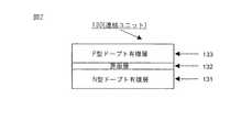
隣接有機ELユニット間に設けられる連結ユニットは、当該隣接有機ELユニットへ効率的に電子及び正孔を注入することが要求されるため、きわめて重要である。連結ユニットの層構造を図2に示す。連結ユニットは、順に、n型ドープト有機層131、界面層132及びp型ドープト有機層133を含んで成る。n型ドープト有機層131は、有機ELユニットのアノード側にあるETLに隣接し、そしてp型ドープト有機層133は、有機ELユニットのカソード側にあるHTLに隣接する。n型ドープト有機層は、隣接する電子輸送層に効率的に電子を注入するように選ばれる。p型ドープト有機層は、隣接する正孔輸送層に効率的に正孔を注入するように選ばれる。連結ユニットにおいて界面層を使用するのは、n型ドープト有機層とp型ドープト有機層との間で起こり得る相互拡散又は反応を防止するためである。カスケード式OLEDの動作特性を維持するため、この追加される界面層が、電気抵抗を上昇させたり、光学的透明性を低下させたりすることがあってはならない。そうでないと駆動電圧が上昇し、また光出力が低下してしまう。したがって、当該界面層は、スペクトルの可視領域において90%以上の光透過率を有する。当該界面層の化学組成及び厚さは、拡散遮断性と光学特性の双方に影響を及ぼすので、最適化する必要がある。特に有機層は付着に際して劣化を受けやすいので、付着方法についても最適化する必要がある。 The connecting unit provided between adjacent organic EL units is extremely important because it is required to efficiently inject electrons and holes into the adjacent organic EL unit. FIG. 2 shows the layer structure of the connection unit. The connection unit includes, in order, an n-type doped
n型ドープト有機層とは、当該層が導電性であり、かつ、その電荷担体が主として電子であることを意味する。当該導電性は、ドーパントからホスト材料へ電子が移動する結果として電荷移動錯体が形成されることによって付与される。電子をホスト材料へ供与する際の当該ドーパントの濃度及び有効性に依存して、当該層の導電性は半導体性から導体性までの範囲をとり得る。同様に、p型ドープト有機層とは、当該層が導電性であり、かつ、その電荷担体が主として正孔であることを意味する。当該導電性は、ドーパントからホスト材料へ正孔が移動する結果として電荷移動錯体が形成されることによって付与される。正孔をホスト材料へ供与する際の当該ドーパントの濃度及び有効性に依存して、当該層の導電性は半導体性から導体性までの範囲をとり得る。 An n-type doped organic layer means that the layer is conductive and its charge carriers are mainly electrons. The conductivity is imparted by the formation of a charge transfer complex as a result of the transfer of electrons from the dopant to the host material. Depending on the concentration and effectiveness of the dopant in donating electrons to the host material, the conductivity of the layer can range from semiconducting to conductive. Similarly, a p-type doped organic layer means that the layer is conductive and its charge carriers are mainly holes. The conductivity is imparted by the formation of a charge transfer complex as a result of the transfer of holes from the dopant to the host material. Depending on the concentration and effectiveness of the dopant in donating holes to the host material, the conductivity of the layer can range from semiconducting to conductive.
各連結ユニットにおけるn型ドープト有機層は、ホスト有機材料及び少なくとも1種のn型ドーパントを含む。n型ドープト有機層に含まれるホスト材料は、低分子材料もしくは高分子材料又はそれらの組合せを含む。このホスト材料が電子輸送を支援し得ることが好ましい。各連結ユニットにおけるp型ドープト有機層は、ホスト有機材料及び少なくとも1種のp型ドーパントを含む。当該ホスト材料は、低分子材料もしくは高分子材料又はそれらの組合せを含む。このホスト材料が正孔輸送を支援し得ることが好ましい。一般に、n型ドープト有機層のためのホスト材料とp型ドープト有機層のためのホスト材料とは、伝導の種類が違うため、異なるものとなる。しかしながら、場合によって、有機材料の中には、n型ドープト有機層又はp型ドープト有機層のいずれにおいてもホストとして使用できるものがある。こうした材料は正孔又は電子のどちらの輸送も支援することができる。適当なn型ドーパント又はp型ドーパントをドーピングすると、当該ドープト有機層は、それぞれ電子輸送性又は正孔輸送性を主に示すようになる。n型又はp型のドーピング濃度は、0.01〜20体積%の範囲内にすることが好ましい。各連結ユニットの全体厚は、典型的には200nm未満であり、好ましくは約1〜150nmの範囲内である。 The n-type doped organic layer in each connection unit includes a host organic material and at least one n-type dopant. The host material included in the n-type doped organic layer includes a low molecular material or a high molecular material, or a combination thereof. Preferably, the host material can support electron transport. The p-type doped organic layer in each connection unit includes a host organic material and at least one p-type dopant. The host material includes a low molecular weight material or a high molecular weight material or a combination thereof. Preferably, the host material can support hole transport. Generally, the host material for an n-type doped organic layer and the host material for a p-type doped organic layer are different because of the different types of conduction. However, in some cases, some organic materials can be used as hosts in either the n-type doped organic layer or the p-type doped organic layer. Such materials can assist in transporting either holes or electrons. When doped with an appropriate n-type dopant or p-type dopant, the doped organic layer mainly exhibits an electron transporting property or a hole transporting property, respectively. The n-type or p-type doping concentration is preferably in the range of 0.01 to 20% by volume. The total thickness of each connecting unit is typically less than 200 nm, and preferably is in the range of about 1 to 150 nm.
従来型のOLEDデバイスに使用されている電子輸送性材料が、n型ドープト有機層のためのホスト材料として有用な種類を代表する。好適な材料は、オキシン(通称8-キノリノール又は8-ヒドロキシキノリン)それ自体のキレートをはじめとする金属キレート化オキシノイド系化合物、例えばトリス(8-ヒドロキシキノリン)アルミニウム、である。他の材料として、Tangの米国特許第4356429号明細書に記載されている各種ブタジエン誘導体、Van Slykeらの米国特許第4539507号明細書に記載されている各種複素環式蛍光増白剤、トリアジン、ヒドロキシキノリン誘導体、及びベンズアゾール誘導体が挙げられる。また、シロール誘導体、例えば、村田ら(Applied Physics Letters, 80, 189, 2002)が報告した2,5-ビス(2',2"-ビピリジン-6-イル)-1,1-ジメチル-3,4-ジフェニルシラシクロペンタジエンも、有用なホスト材料である。 Electron transporting materials used in conventional OLED devices represent a useful class of host materials for n-type doped organic layers. Suitable materials are metal chelated oxinoid-based compounds, including chelates of oxine (commonly known as 8-quinolinol or 8-hydroxyquinoline) itself, such as aluminum tris (8-hydroxyquinoline). Other materials include various butadiene derivatives described in Tang U.S. Pat. No. 4,356,429, various heterocyclic optical brighteners described in Van Slyke et al., U.S. Pat. Examples include hydroxyquinoline derivatives and benzazole derivatives. Also, silole derivatives such as 2,5-bis (2 ', 2 "-bipyridin-6-yl) -1,1-dimethyl-3, reported by Murata et al. (Applied Physics Letters, 80, 189, 2002). 4-Diphenylsilacyclopentadiene is also a useful host material.
連結ユニットのn型ドープト有機層においてn型ドーパントとして使用される材料には、仕事関数が4.0eV未満である金属又は金属化合物が含まれる。特に有用なドーパントとして、アルカリ金属、アルカリ金属化合物、アルカリ土類金属及びアルカリ土類金属化合物が挙げられる。用語「金属化合物」には、有機金属錯体、金属有機塩並びに無機の塩、酸化物及びハロゲン化物が包含される。含金属n型ドーパントの種類の中では、特に、Li, Na, K, Rb, Cs, Mg, Ca, Sr, Ba, La, Ce, Sm, Eu, Tb, Dy又はYb及びこれらの無機化合物又は有機化合物が有用である。また、連結ユニットのn型ドープト有機層においてn型ドーパントとして使用される材料には、電子供与性が強い有機還元剤も含まれる。「電子供与性が強い」とは、当該有機ドーパントが、当該ホストとの電荷移動錯体を形成するため当該ホストに対して少なくとも一部の電子的電荷を供与できなければならないことを意味する。有機分子の非限定例として、ビス(エチレンジチオ)-テトラチアフルバレン(BEDT-TTF)、テトラチアフルバレン(TTF)及びそれらの誘導体が挙げられる。高分子ホストの場合には、当該ドーパントは、上記のいずれであってもよく、また当該ホストに対して、少量成分として、分子レベルで分散される又は共重合される材料であってもよい。 Materials used as n-type dopants in the n-type doped organic layer of the linking unit include metals or metal compounds having a work function of less than 4.0 eV. Particularly useful dopants include alkali metals, alkali metal compounds, alkaline earth metals and alkaline earth metal compounds. The term "metal compounds" includes organometallic complexes, metal organic salts and inorganic salts, oxides and halides. Among the types of metal-containing n-type dopants, in particular, Li, Na, K, Rb, Cs, Mg, Ca, Sr, Ba, La, Ce, Sm, Eu, Tb, Dy or Yb and their inorganic compounds or Organic compounds are useful. The material used as the n-type dopant in the n-type doped organic layer of the connection unit also includes an organic reducing agent having a strong electron-donating property. "Strong electron donating" means that the organic dopant must be able to donate at least some electronic charge to the host to form a charge transfer complex with the host. Non-limiting examples of organic molecules include bis (ethylenedithio) -tetrathiafulvalene (BEDT-TTF), tetrathiafulvalene (TTF) and derivatives thereof. In the case of a polymer host, the dopant may be any of the above, and may be a material that is dispersed or copolymerized at a molecular level as a minor component with respect to the host.
従来型のOLEDデバイスに使用されている正孔輸送性材料が、p型ドープト有機層のためのホスト材料として有用な種類を代表する。好適な材料として、少なくとも一つが芳香族環の環員である炭素原子にのみ結合している3価窒素原子を1個以上含有する芳香族第三アミンが挙げられる。一つの形態として、芳香族第三アミンはアリールアミン、例えば、モノアリールアミン、ジアリールアミン、トリアリールアミン又は高分子アリールアミンであることができる。1以上のビニル基で置換された、及び/又は少なくとも一つの活性水素含有基を含む、その他の好適なトリアリールアミンが、Brantleyら(米国特許第3567450号及び同第3658520号明細書)に記載されている。より好ましい種類の芳香族第三アミンは、Van Slykeら(米国特許第4720432号及び同第5061569号明細書)に記載されているような、2以上の芳香族第三アミン部分を含むものである。非限定例として、N,N'-ジ(ナフタレン-1-イル)-N,N'-ジフェニル-ベンジジン(NPB)、N,N'-ジフェニル-N,N'-ビス(3-メチルフェニル)-1,1-ビフェニル-4,4'-ジアミン(TPD)及びN,N,N',N'-テトラナフチル-ベンジジン(TNB)が挙げられる。 Hole transporting materials used in conventional OLED devices represent a useful class of host materials for p-type doped organic layers. Suitable materials include aromatic tertiary amines containing one or more trivalent nitrogen atoms, at least one of which is attached only to a carbon atom that is a ring member of an aromatic ring. In one form, the aromatic tertiary amine can be an arylamine, for example, a monoarylamine, diarylamine, triarylamine or polymeric arylamine. Other suitable triarylamines substituted with one or more vinyl groups and / or containing at least one active hydrogen-containing group are described in Brantley et al. (US Pat. Nos. 3,567,450 and 3,658,520). Have been. A more preferred class of aromatic tertiary amines are those containing two or more aromatic tertiary amine moieties, as described in Van Slyke et al. (US Pat. Nos. 4,720,432 and 5,061,569). Non-limiting examples include N, N'-di (naphthalen-1-yl) -N, N'-diphenyl-benzidine (NPB), N, N'-diphenyl-N, N'-bis (3-methylphenyl) -1,1-biphenyl-4,4′-diamine (TPD) and N, N, N ′, N′-tetranaphthyl-benzidine (TNB).
連結ユニットのp型ドープト有機層においてp型ドーパントとして使用される材料には、電子求引性が強い酸化剤が含まれる。「電子求引性が強い」とは、当該有機ドーパントが、当該ホストとの電荷移動錯体を形成するため当該ホストから一部の電子的電荷を受容できなければならないことを意味する。非限定例の一部として、2,3,5,6-テトラフルオロ-7,7,8,8-テトラシアノキノジメタン(F4-TCNQ)その他TCNQの誘導体のような有機化合物、及びヨウ素、FeCl3、FeF3、SbCl5その他の金属ハロゲン化物の一部のような無機酸化剤が挙げられる。高分子ホストの場合には、当該ドーパントは、上記のいずれであってもよく、また当該ホストに対して、少量成分として、分子レベルで分散される又は共重合される材料であってもよい。The material used as the p-type dopant in the p-type doped organic layer of the connection unit includes an oxidant having a strong electron-withdrawing property. “Strong electron-withdrawing” means that the organic dopant must be able to accept some electronic charge from the host to form a charge transfer complex with the host. Some non-limiting examples include organic compounds such as 2,3,5,6-tetrafluoro-7,7,8,8-tetracyanoquinodimethane (F4 -TCNQ) and other derivatives of TCNQ, and iodine , FeCl3 , FeF3 , SbCl5 and other inorganic halides such as some of the metal halides. In the case of a polymer host, the dopant may be any of the above, and may be a material that is dispersed or copolymerized at a molecular level as a minor component with respect to the host.
n型又はp型のどちらのドープト有機層のホストにも使用することができる材料の例として、米国特許第5972247号明細書に記載されている各種アントラセン誘導体、4,4-ビス(9-ジカルバゾリル)-ビフェニル(CBP)のような特定のカルバゾール誘導体、及び米国特許第5121029号明細書に記載されている4,4'-ビス(2,2'-ジフェニルビニル)-1,1'-ビフェニルのようなジスチリルアリーレン誘導体が挙げられるが、これらに限定はされない。 Examples of materials that can be used as hosts for either n-type or p-type doped organic layers include various anthracene derivatives described in US Pat. No. 5,972,247, and 4,4-bis (9-dicarbazolyl). ) -Biphenyl (CBP) and certain carbazole derivatives and 4,4′-bis (2,2′-diphenylvinyl) -1,1′-biphenyl described in US Pat. No. 5,121,029. Such distyrylarylene derivatives can be mentioned, but are not limited thereto.
連結ユニットにおいて有用な界面層132は、少なくとも1種の無機半導体又は該半導体を2種以上組み合わせたものを含む。好適な半導体は、電子エネルギーバンドギャップが4.0eV未満でなければならない。電子エネルギーバンドギャップは、当該分子の最高被占軌道と最低空軌道との間のエネルギー差として定義される。有用な種類の材料は、元素周期律表(例、VWR Scientific Productsの刊行物である元素周期律表)の第IVA族、第VA族、第VIA族、第VIIA族、第VIIIA族、第IB族、第IIB族、第IIIB族、第IVB族及び第VB族に列挙されている元素の化合物の中から選ぶことができる。これらの化合物には、炭化物、珪化物、窒化物、リン化物、ヒ化物、酸化物、硫化物、セレン化物及びテルル化物並びにこれらの混合物が含まれる。これらの半導体化合物は、化学量論状態であっても非化学量論状態であってもよい。すなわち、含まれる金属成分が過剰であったり欠乏したりしていてもよい。界面層132に特に有用な材料として、チタン、ジルコニウム、ハフニウム、バナジウム、ニオブ、タンタル、クロム、モリブデン、タングステン、マンガン、レニウム、鉄、ルテニウム、オスミウム、コバルト、ロジウム、イリジウム、ニッケル、パラジウム、白金、銅、亜鉛、カドミウム、ガリウム、タリウム、珪素、ゲルマニウム、鉛及びアンチモンの半導体酸化物又はこれらの組合せが挙げられる。界面層132に特に有用な材料には、セレン化亜鉛、窒化ガリウム、炭化珪素又はこれらの組合せが含まれる。 The
連結ユニットにおいて有用な界面層132は、少なくとも1種以上の金属材料を含むことができ、SzeのPhysics of Semiconducting Devices、第2版、Wiley、N.Y.、1981、第251頁に記載されているように、これら金属材料の少なくとも1種は4.0eVより高い仕事関数を有する。 The
連結ユニットの構築に適した界面層132の厚さは0.05nm〜10nmの範囲内にある。好ましくは、当該範囲は、無機半導体の場合は0.1nm〜5nmであり、また金属材料の場合は0.05nm〜1nmである。 The thickness of the
連結ユニットの構築に適した界面層132は、熱蒸発法、電子ビーム蒸発法又はイオンスパッタ蒸着法によって加工製作される。界面層132は、有機層を付着させる方法に適合する熱蒸発法によって加工製作されることが好ましい。 The
本発明のカスケード式OLEDは、カソード又はアノードのいずれが接触していてもよい支持基板の上に設けられることが典型的である。基板に接している電極を、便宜上、底部電極と称する。底部電極をアノードにすることが慣例的であるが、本発明はそのような構成に限定されるものではない。基板は、意図される発光方向に依存して、透光性又は不透明のいずれかであることができる。基板を介してEL発光を観察する場合には透光性が望まれる。このような場合、透明なガラス又はプラスチックが通常用いられる。上部電極を介してEL発光を観察する用途の場合には、底部支持体の透過性は問題とならないため、透光性、吸光性又は光反射性のいずれであってもよい。この場合の用途向け基板には、ガラス、プラスチック、半導体材料、シリコン、セラミックス及び回路基板材料が含まれるが、これらに限定はされない。もちろん、このようなデバイス構成には、透光性の上部電極を提供する必要はある。 Typically, the cascaded OLEDs of the present invention are provided on a support substrate that may be in contact with either the cathode or the anode. The electrode in contact with the substrate is called the bottom electrode for convenience. It is customary for the bottom electrode to be the anode, but the invention is not limited to such a configuration. The substrate can be either translucent or opaque, depending on the intended direction of light emission. When observing EL light emission through a substrate, translucency is desired. In such cases, clear glass or plastic is commonly used. In the case of observing the EL light emission through the upper electrode, the transmittance of the bottom support is not a problem, and therefore, any of light-transmitting, light-absorbing, and light-reflecting materials may be used. Application substrates in this case include, but are not limited to, glass, plastic, semiconductor materials, silicon, ceramics, and circuit board materials. Of course, such device configurations require the provision of a translucent top electrode.
アノード110は、これを介してEL発光を観察する場合には、当該発光に対して透明又は実質的に透明であることが必要である。本発明に用いられる一般的な透明アノード材料はインジウム錫酸化物(ITO)、インジウム亜鉛酸化物(IZO)及び酸化錫であるが、例示としてアルミニウム又はインジウムをドープした酸化亜鉛、マグネシウムインジウム酸化物及びニッケルタングステン酸化物をはじめとする他の金属酸化物でも使用することができる。これらの酸化物の他、窒化ガリウムのような金属窒化物、セレン化亜鉛のような金属セレン化物、及び硫化亜鉛のような金属硫化物をアノードとして使用することもできる。カソード電極を介してのみEL発光を観察する用途の場合には、アノードの透過性は問題とならず、透明、不透明又は反射性を問わずいずれの導電性材料でも使用することができる。このような用途向けの導体の例として、金、イリジウム、モリブデン、パラジウム及び白金が挙げられるが、これらに限定はされない。典型的なアノード材料は、透過性であってもそうでなくても、4.0eVより高い仕事関数を有する。望ましいアノード材料は、一般に、蒸発法、スパッタ法、化学的気相成長(CVD)法又は電気化学法のような適当な手段のいずれかによって付着される。アノードは、周知のフォトリソグラフ法によってパターン化することもできる。必要に応じ、短絡を極力抑え、又は反射性を高めるために、他の層を適用する前にアノードを磨き、その表面粗さを低下させてもよい。 When observing EL emission through this, the
常に必要であるわけではないが、第1番目の有機ELユニットに、アノード110と接触するようにHILを設けることがしばしば有用となる。HILは、後続の有機層の薄膜形成性を改良し、かつ、HTLへの正孔注入を促進することにより、カスケード式OLEDの駆動電圧を低下させるのに役立つことができる。HILに用いるのに好適な材料として、米国特許第4720432号明細書に記載されているポルフィリン系化合物、米国特許第6208075号明細書に記載されているプラズマ蒸着フルオロカーボンポリマー、及びある種の芳香族アミン、例えば、m-MTDATA(4,4',4"-トリス[(3-エチルフェニル)フェニルアミノ]トリフェニルアミン)が挙げられるが、これらに限定はされない。米国特許第6423429号に記載されているように、上記の連結ユニットにおいて使用されるp型ドープト有機層も有用である。有機ELデバイスに有用であることが報告されている別の代わりの正孔注入性材料が、欧州特許出願公開第0891121号及び同第1029909号明細書に記載されている。 Although not always necessary, it is often useful to provide the first organic EL unit with HIL in contact with the
有機ELユニットのHTLは、芳香族第三アミンのような少なくとも1種の正孔輸送性化合物を含む。芳香族第三アミンとは、少なくとも一つが芳香族環の環員である炭素原子にのみ結合している3価窒素原子を1個以上含有する化合物であると解される。一つの形態として、芳香族第三アミンはアリールアミン、例えば、モノアリールアミン、ジアリールアミン、トリアリールアミン又は高分子アリールアミンであることができる。トリアリールアミン単量体の例が、米国特許第3180730号(Klupfelら)に示されている。1以上のビニル基で置換された、及び/又は少なくとも一つの活性水素含有基を含む、その他の好適なトリアリールアミンが、Brantleyらの米国特許第3567450号及び同第3658520号に記載されている。 The HTL of the organic EL unit contains at least one hole transporting compound such as an aromatic tertiary amine. Aromatic tertiary amines are understood to be compounds containing one or more trivalent nitrogen atoms, at least one of which is bound only to carbon atoms which are ring members of an aromatic ring. In one form, the aromatic tertiary amine can be an arylamine, for example, a monoarylamine, diarylamine, triarylamine or polymeric arylamine. Examples of triarylamine monomers are given in U.S. Pat. No. 3,180,730 (Klupfel et al.). Other suitable triarylamines substituted with one or more vinyl groups and / or containing at least one active hydrogen-containing group are described in Brantley et al., US Pat. Nos. 3,567,450 and 3,658,520. .
より好ましい種類の芳香族第三アミンは、米国特許第4720432号及び同第5061569号に記載されているような芳香族第三アミン部分を2個以上含有するものである。HTLは、芳香族第三アミン化合物の単体又は混合物で形成することができる。有用な芳香族第三アミンを例示する。 A more preferred class of aromatic tertiary amines are those containing two or more aromatic tertiary amine moieties as described in U.S. Patent Nos. 4,720,432 and 5,061,569. The HTL can be formed from an aromatic tertiary amine compound alone or as a mixture. Illustrative of useful aromatic tertiary amines.
1,1-ビス(4-ジ-p-トリルアミノフェニル)シクロヘキサン
1,1-ビス(4-ジ-p-トリルアミノフェニル)-4-フェニルシクロヘキサン
4,4’-ビス(ジフェニルアミノ)クアドリフェニル
ビス(4-ジメチルアミノ-2-メチルフェニル)-フェニルメタン
N,N,N-トリ(p-トリル)アミン
4-(ジ-p-トリルアミノ)-4’-[4(ジ-p-トリルアミノ)-スチリル]スチルベン
N,N,N’,N’-テトラ-p-トリル-4,4’-ジアミノビフェニル
N,N,N’,N’-テトラフェニル-4,4’-ジアミノビフェニル
N,N,N’,N’-テトラ-1-ナフチル-4,4’-ジアミノビフェニル
N,N,N’,N’-テトラ-2-ナフチル-4,4’-ジアミノビフェニル
N-フェニルカルバゾール
4,4’-ビス[N-(1-ナフチル)-N-フェニルアミノ]ビフェニル
4,4’-ビス[N-(1-ナフチル)-N-(2-ナフチル)アミノ]ビフェニル
4,4”-ビス[N-(1-ナフチル)-N-フェニルアミノ]-p-ターフェニル
4,4’-ビス[N-(2-ナフチル)-N-フェニルアミノ]ビフェニル
4,4’-ビス[N-(3-アセナフテニル)-N-フェニルアミノ]ビフェニル
1,5-ビス[N-(1-ナフチル)-N-フェニルアミノ]ナフタレン
4,4’-ビス[N-(9-アントリル)-N-フェニルアミノ]ビフェニル
4,4”-ビス[N-(1-アントリル)-N-フェニルアミノ]-p-ターフェニル
4,4’-ビス[N-(2-フェナントリル)-N-フェニルアミノ]ビフェニル
4,4’-ビス[N-(8-フルオルアンテニル)-N-フェニルアミノ]ビフェニル
4,4’-ビス[N-(2-ピレニル)-N-フェニルアミノ]ビフェニル
4,4’-ビス[N-(2-ナフタセニル)-N-フェニルアミノ]ビフェニル
4,4’-ビス[N-(2-ペリレニル)-N-フェニルアミノ]ビフェニル
4,4’-ビス[N-(1-コロネニル)-N-フェニルアミノ]ビフェニル
2,6-ビス(ジ-p-トリルアミノ)ナフタレン
2,6-ビス[ジ-(1-ナフチル)アミノ]ナフタレン
2,6-ビス[N-(1-ナフチル)-N-(2-ナフチル)アミノ]ナフタレン
N,N,N’,N’-テトラ(2-ナフチル)-4,4”-ジアミノ-p-ターフェニル
4,4’-ビス{N-フェニル-N-[4-(1-ナフチル)-フェニル]アミノ}ビフェニル
4,4’-ビス[N-フェニル-N-(2-ピレニル)アミノ]ビフェニル
2,6-ビス[N,N-ジ(2-ナフチル)アミン]フルオレン
1,5-ビス[N-(1-ナフチル)-N-フェニルアミノ]ナフタレン
4,4',4"-トリス[(3-メチルフェニル)フェニルアミノ]トリフェニルアミン1,1-bis (4-di-p-tolylaminophenyl) cyclohexane
1,1-bis (4-di-p-tolylaminophenyl) -4-phenylcyclohexane
4,4'-bis (diphenylamino) quadriphenyl bis (4-dimethylamino-2-methylphenyl) -phenylmethane
N, N, N-tri (p-tolyl) amine
4- (di-p-tolylamino) -4 '-[4 (di-p-tolylamino) -styryl] stilbene
N, N, N ', N'-tetra-p-tolyl-4,4'-diaminobiphenyl
N, N, N ', N'-tetraphenyl-4,4'-diaminobiphenyl
N, N, N ', N'-tetra-1-naphthyl-4,4'-diaminobiphenyl
N, N, N ', N'-tetra-2-naphthyl-4,4'-diaminobiphenyl
N-phenylcarbazole
4,4'-bis [N- (1-naphthyl) -N-phenylamino] biphenyl
4,4'-bis [N- (1-naphthyl) -N- (2-naphthyl) amino] biphenyl
4,4 ”-bis [N- (1-naphthyl) -N-phenylamino] -p-terphenyl
4,4'-bis [N- (2-naphthyl) -N-phenylamino] biphenyl
4,4'-bis [N- (3-acenaphthenyl) -N-phenylamino] biphenyl
1,5-bis [N- (1-naphthyl) -N-phenylamino] naphthalene
4,4'-bis [N- (9-anthryl) -N-phenylamino] biphenyl
4,4 ”-bis [N- (1-anthryl) -N-phenylamino] -p-terphenyl
4,4'-bis [N- (2-phenanthryl) -N-phenylamino] biphenyl
4,4'-bis [N- (8-fluoroantenyl) -N-phenylamino] biphenyl
4,4'-bis [N- (2-pyrenyl) -N-phenylamino] biphenyl
4,4'-bis [N- (2-naphthacenyl) -N-phenylamino] biphenyl
4,4'-bis [N- (2-perylenyl) -N-phenylamino] biphenyl
4,4'-bis [N- (1-colonenyl) -N-phenylamino] biphenyl
2,6-bis (di-p-tolylamino) naphthalene
2,6-bis [di- (1-naphthyl) amino] naphthalene
2,6-bis [N- (1-naphthyl) -N- (2-naphthyl) amino] naphthalene
N, N, N ', N'-tetra (2-naphthyl) -4,4 "-diamino-p-terphenyl
4,4'-bis {N-phenyl-N- [4- (1-naphthyl) -phenyl] amino} biphenyl
4,4'-bis [N-phenyl-N- (2-pyrenyl) amino] biphenyl
2,6-bis [N, N-di (2-naphthyl) amine] fluorene
1,5-bis [N- (1-naphthyl) -N-phenylamino] naphthalene
4,4 ', 4 "-tris [(3-methylphenyl) phenylamino] triphenylamine
別の種類の有用な正孔輸送性材料として、欧州特許第1009041号に記載されているような多環式芳香族化合物が挙げられる。オリゴマー材料をはじめとする、アミン基を3個以上含有する芳香族第三アミンを使用してもよい。さらに、ポリ(N-ビニルカルバゾール)(PVK)、ポリチオフェン、ポリピロール、ポリアニリン及びPEDOT/PSSとも呼ばれているポリ(3,4-エチレンジオキシチオフェン)/ポリ(4-スチレンスルホネート)のようなコポリマー、といった高分子正孔輸送性材料を使用することもできる。 Another class of useful hole-transporting materials includes polycyclic aromatic compounds as described in EP 1009041. Aromatic tertiary amines containing three or more amine groups, including oligomeric materials, may be used. In addition, copolymers such as poly (N-vinylcarbazole) (PVK), polythiophene, polypyrrole, polyaniline and poly (3,4-ethylenedioxythiophene) / poly (4-styrenesulfonate), also called PEDOT / PSS For example, a polymer hole transporting material such as.
米国特許第4769292号及び同第5935721号に詳述されているように、有機ELユニットのLELは発光材料又は蛍光材料を含み、その領域において電子-正孔対が再結合する結果として電場発光が生じる。LELは、単一材料で構成することもできるが、より一般的には、ホスト材料に単一又は複数種のゲスト化合物をドーピングしてなり、そこで主として当該ドーパントから発光が生じ、その発光色にも制限はない。LELに含まれるホスト材料は、後述する電子輸送性材料、上述した正孔輸送性材料、又は正孔-電子再結合を支援する別の材料もしくはその組合せ、であることができる。ドーパントは、通常は高蛍光性色素の中から選ばれるが、リン光性化合物、例えば、国際公開第98/55561号、同第00/18851号、同第00/57676号及び同第00/70655号に記載されているような遷移金属錯体も有用である。ドーパントは、ホスト材料中、0.01〜10質量%の範囲内でコーティングされることが典型的である。ホスト材料として、ポリフルオレンやポリビニルアリーレン(例、ポリ(p-フェニレンビニレン)、PPV)のような高分子材料を使用することもできる。この場合、高分子ホスト中に低分子ドーパントを分子レベルで分散させること、又はホストポリマー中に二次成分を共重合させることによりドーパントを付加すること、が可能である。 As described in detail in U.S. Pat. Nos. 4,769,292 and 5,935,721, the LEL of an organic EL unit includes a luminescent or fluorescent material in which electro-hole pairs recombine in the region resulting in electroluminescence. Occurs. The LEL can be composed of a single material, but more generally, a host material is doped with a single or plural kinds of guest compounds, where light emission mainly occurs from the dopant and the emission color is increased. There are no restrictions. The host material included in the LEL can be an electron transporting material as described below, a hole transporting material as described above, or another material that supports hole-electron recombination or a combination thereof. The dopant is usually selected from highly fluorescent dyes, but phosphorescent compounds such as WO 98/55561, WO 00/18851, WO 00/57676 and WO 00/70655. Also useful are transition metal complexes as described in US Pat. Typically, the dopant is coated within the range of 0.01 to 10% by mass in the host material. As the host material, a polymer material such as polyfluorene or polyvinylarylene (eg, poly (p-phenylenevinylene), PPV) can be used. In this case, it is possible to disperse the low-molecular dopant in the polymer host at the molecular level, or to add the dopant by copolymerizing a secondary component in the host polymer.
ドーパントとしての色素を選定するための重要な関係は、当該分子の最高被占軌道と最低空軌道との間のエネルギー差として定義されるバンドギャップポテンシャルの対比である。ホストからドーパント分子へのエネルギー伝達の効率化を図るためには、当該ドーパントのバンドギャップがホスト材料のそれよりも小さいことが必須条件となる。リン光性発光体の場合には、ホストの三重項エネルギー準位が、ホストからドーパントへのエネルギー移動を可能ならしめるに十分な高さであることも重要である。 An important relationship for choosing a dye as a dopant is the contrast of the bandgap potential, defined as the energy difference between the highest occupied orbital and the lowest unoccupied orbital of the molecule. In order to improve the efficiency of energy transfer from the host to the dopant molecule, it is an essential condition that the band gap of the dopant is smaller than that of the host material. In the case of phosphorescent emitters, it is also important that the triplet energy level of the host be high enough to allow energy transfer from the host to the dopant.
有用性が知られているホスト及び発光性分子として、米国特許第4769292号、同第5141671号、同第5150006号、同第5151629号、同第5405709号、同第5484922号、同第5593788号、同第5645948号、同第5683823号、同第5755999号、同第5928802号、同第5935720号、同第5935721号及び同第6020078号に記載されているものが挙げられるが、これらに限定はされない。 As useful hosts and light-emitting molecules, US Pat. Nos. 4,769,292, 5,141,671, 5,515,0006, 5,151,629, 5,405,709, 5,484,922, 5,593,788, No. 5,645,948, No. 5,683,823, No. 5,755,999, No. 5,929,802, No. 5,935,720, No. 5,935,721, and No. 6,035,078, but are not limited thereto. .
8-ヒドロキシキノリン(オキシン)及び類似の誘導体の金属錯体は、電場発光を支援することができる有用なホスト化合物の一種である。以下、有用なキレート化オキシノイド系化合物の例を示す。
CO-1:アルミニウムトリスオキシン〔別名、トリス(8-キノリノラト)アルミニウム(III)〕
CO-2:マグネシウムビスオキシン〔別名、ビス(8-キノリノラト)マグネシウム(II)〕
CO-3:ビス[ベンゾ{f}-8-キノリノラト]亜鉛(II)
CO-4:ビス(2-メチル-8-キノリノラト)アルミニウム(III)-μ-オキソ-ビス(2-メチル-8-キノリノラト)アルミニウム(III)
CO-5:インジウムトリスオキシン〔別名、トリス(8-キノリノラト)インジウム〕
CO-6:アルミニウムトリス(5-メチルオキシン)〔別名、トリス(5-メチル-8-キノリノラト)アルミニウム(III)〕
CO-7:リチウムオキシン〔別名、(8-キノリノラト)リチウム(I)〕
CO-8:ガリウムオキシン〔別名、トリス(8-キノリノラト)ガリウム(III)〕
CO-9:ジルコニウムオキシン〔別名、テトラ(8-キノリノラト)ジルコニウム(IV)〕Metal complexes of 8-hydroxyquinoline (oxine) and similar derivatives are a class of useful host compounds that can support electroluminescence. The following are examples of useful chelated oxinoid compounds.
CO-1: Aluminum trisoxine [also known as tris (8-quinolinolato) aluminum (III)]
CO-2: magnesium bisoxin [also known as bis (8-quinolinolato) magnesium (II)]
CO-3: bis [benzo {f} -8-quinolinolato] zinc (II)
CO-4: Bis (2-methyl-8-quinolinolato) aluminum (III) -μ-oxo-bis (2-methyl-8-quinolinolato) aluminum (III)
CO-5: Indium trisoxin [also known as tris (8-quinolinolato) indium]
CO-6: aluminum tris (5-methyloxin) [also known as tris (5-methyl-8-quinolinolato) aluminum (III)]
CO-7: lithium oxine [also known as (8-quinolinolato) lithium (I)]
CO-8: gallium oxine [also known as tris (8-quinolinolato) gallium (III)]
CO-9: zirconium oxine [also known as tetra (8-quinolinolato) zirconium (IV)]
有用なホスト材料の別の種類として、米国特許第5935721号に記載されている9,10-ジ-(2-ナフチル)アントラセン及びその誘導体のようなアントラセン誘導体、米国特許第5121029号に記載されているジスチリルアリーレン誘導体、並びに2,2’,2”-(1,3,5-フェニレン)トリス[1-フェニル-1H-ベンズイミダゾール]のようなベンズアゾール誘導体が挙げられるが、これらに限定はされない。リン光性発光体の場合には、カルバゾール誘導体が特に有用なホストとなる。 Another class of useful host materials is an anthracene derivative such as 9,10-di- (2-naphthyl) anthracene and its derivatives described in U.S. Patent No. 5,935,721, described in U.S. Patent No. But also benzazole derivatives such as 2,2 ′, 2 ″-(1,3,5-phenylene) tris [1-phenyl-1H-benzimidazole], but are not limited thereto. In the case of phosphorescent emitters, carbazole derivatives are particularly useful hosts.
有用な蛍光性ドーパントには、アントラセン、テトラセン、キサンテン、ペリレン、ルブレン、クマリン、ローダミン、キナクリドン、ジシアノメチレンピラン、チオピラン、ポリメチン、ピリリウム及びチアピリリウムの各化合物の誘導体、フルオレン誘導体、ペリフランテン誘導体、インデノペリレン誘導体、ビス(アジニル)アミンホウ素化合物、ビス(アジニル)メタン化合物並びにカルボスチリル化合物が包含される。 Useful fluorescent dopants include derivatives of anthracene, tetracene, xanthene, perylene, rubrene, coumarin, rhodamine, quinacridone, dicyanomethylenepyran, thiopyran, polymethine, pyrylium and thiapyrylium compounds, fluorene derivatives, periflanthene derivatives, indenoperylene Derivatives, bis (azinyl) amine boron compounds, bis (azinyl) methane compounds and carbostyril compounds are included.
本発明の有機ELユニットのETLを形成するのに用いるのに好ましい薄膜形成性材料は、オキシン(通称8-キノリノール又は8-ヒドロキシキノリン)それ自体のキレートをはじめとする金属キレート化オキシノイド系化合物である。このような化合物は、電子の注入及び輸送を助長し、しかも高い性能レベルを示すと共に、薄膜への加工が容易である。オキシノイド系化合物の例は先に列挙した通り。 Preferred thin film-forming materials for use in forming the ETL of the organic EL unit of the present invention are metal chelated oxinoid compounds, including chelates of oxine (commonly known as 8-quinolinol or 8-hydroxyquinoline) itself. is there. Such compounds facilitate electron injection and transport, exhibit high performance levels, and are easy to process into thin films. Examples of oxinoid compounds are as listed above.
その他の電子輸送性材料として、米国特許第4356429号に記載されている各種ブタジエン誘導体、及び米国特許第4539507号に記載されている各種複素環式蛍光増白剤が挙げられる。ベンズアゾール及びトリアジンもまた有用な電子輸送性材料である。 Other electron transporting materials include various butadiene derivatives described in U.S. Pat. No. 4,356,429 and various heterocyclic fluorescent whitening agents described in U.S. Pat. No. 4,539,507. Benzazole and triazine are also useful electron transporting materials.
常に必要であるわけではないが、第N番目の有機ELユニットに、カソード140と接触するようにEILを設けることがしばしば有用となる。EILは、ETLへの電子注入を促進し、かつ、導電性を高めることで、カスケード式OLEDの駆動電圧を低下させるのに役立つことができる。EILに使用するのに好適な材料は、ドーパントとして強還元剤を含む又は、連結ユニットに使用される上記のn型ドープト有機層において記載したドーパントとして低仕事関数(<4.0eV)金属を含む、上記のETLである。有機ELユニットにおいては、後述するように、別の無機電子注入材料が有用となる場合もある。 Although not always necessary, it is often useful to provide an EIL in contact with the
発光をアノードのみを介して観察する場合には、本発明に用いられるカソード層140は、ほとんどすべての導電性材料を含んでなることができる。望ましい材料は、下部の有機層との良好な接触が確保されるよう良好な薄膜形成性を示し、低電圧での電子注入を促進し、かつ、良好な安定性を有する。有用なカソード材料は、低仕事関数金属(<4.0eV)又は合金を含むことが多い。好適なカソード材料の1種に、米国特許第4885221号明細書に記載されているMg:Ag合金(銀含有率1〜20%)を含むものがある。別の好適な種類のカソード材料として、有機層(例、ETL)に接している薄い無機EILに、これより厚い導電性金属層をキャップしてなる二層形が挙げられる。この場合、無機EILは低仕事関数の金属又は金属塩を含むことが好ましく、その場合には、当該より厚いキャップ層は低仕事関数を有する必要はない。このようなカソードの一つに、米国特許第5677572号明細書に記載されている、LiF薄層にこれより厚いAl層を載せてなるものがある。その他の有用なカソード材料のセットとして、米国特許第5059861号、同第5059862号及び同第6140763号明細書に記載されているものが挙げられるが、これらに限定はされない。 When light emission is observed only through the anode, the
カソードを介して発光を観察する場合には、当該カソードは透明又はほぼ透明でなければならない。このような用途の場合、金属が薄くなければならないか、又は透明導電性酸化物もしくはこれら材料の組合せを使用しなければならない。透光性カソードについては、米国特許第4885211号、米国特許第5247190号、米国特許第5703436号、米国特許第5608287号、米国特許第5837391号、米国特許第5677572号、米国特許第5776622号、米国特許第5776623号、米国特許第5714838号、米国特許第5969474号、米国特許第5739545号、米国特許第5981306号、米国特許第6137223号、米国特許第6140763号、米国特許第6172459号、米国特許第6278236号、米国特許第6284393号、JP3234963号及び欧州特許第1076368号に詳しく記載されている。カソード材料は、熱蒸発法、電子ビーム蒸発法、イオンスパッタ法又は化学的気相成長法により付着させることが典型的である。必要な場合には、例えば、マスク介在蒸着法、米国特許第5276380号及び欧州特許出願公開第0732868号明細書に記載の一体型シャドーマスク法、レーザーアブレーション法及び選択的化学的気相成長法をはじめとする多くの周知の方法により、パターンを形成させてもよい。 When light emission is observed through the cathode, the cathode must be transparent or nearly transparent. For such applications, the metal must be thin or a transparent conductive oxide or a combination of these materials must be used. Regarding the translucent cathode, US Pat. No. 4,885,211; US Pat. No. 5,247,190; US Pat. No. 5,703,436; US Pat. No. 5,608,287, US Pat. No. 5,837,391, US Pat. No. 5,677,572, US Pat. U.S. Patent No. 5,776,623; U.S. Patent No. 5,714,838; U.S. Patent No. 5,969,474; U.S. Patent No. 5,795,545; U.S. Patent No. 5,981,306; U.S. Patent No. 6,137,223; U.S. Patent No. 6,140,763; No. 6,278,236, U.S. Pat. No. 6,284,393, JP 32,349,63 and EP 107,368. Cathode materials are typically deposited by thermal evaporation, electron beam evaporation, ion sputtering, or chemical vapor deposition. If necessary, for example, a mask-interposed deposition method, an integrated shadow mask method described in US Pat. No. 5,276,380 and EP-A-0 732 868, a laser ablation method and a selective chemical vapor deposition method can be used. The pattern may be formed by any of a number of well-known methods, including the following.
場合によっては、必要に応じて、有機ELユニットのLELとETLを、発光と電子輸送の両方を支援する機能を発揮する単一層にすることが可能である。当該技術分野では、ホストとして使用できるHTLに発光性ドーパントを添加してもよいことも知られている。白色発光性OLEDを製造するため、1又は2以上の層に複数のドーパントを添加することができ、例えば、青色発光性材料と黄色発光性材料、シアン色発光性材料と赤色発光性材料又は赤色発光性材料と緑色発光性材料と青色発光性材料を組み合わせることができる。白色発光性デバイスについては、例えば、米国特許出願公開第2002/0025419号、米国特許第5683823号、同第5503910号、同第5405709号、同第5283182号、欧州特許第1187235号及び同第1182244号に記載されている。 In some cases, if necessary, the LEL and ETL of the organic EL unit can be formed into a single layer that functions to support both light emission and electron transport. It is also known in the art that a luminescent dopant may be added to an HTL that can be used as a host. To produce a white light emitting OLED, one or more layers can be added with multiple dopants, for example, a blue light emitting material and a yellow light emitting material, a cyan light emitting material and a red light emitting material, or a red light emitting material. A light-emitting material, a green light-emitting material, and a blue light-emitting material can be combined. Regarding white light-emitting devices, for example, US Patent Application Publication No. 2002/0025419, US Pat. No. 5,683,823, US Pat. No. 5,503,910, US Pat. No. 5,405,709, US Pat. No. 5,283,182, EP 1187235 and EP 1182244. It is described in.
本発明のデバイスには、当該技術分野で教示されているような追加の層、例えば、電子阻止層又は正孔阻止層を採用することができる。例えば、米国特許出願公開第2002/0015859号に記載されているように、正孔阻止層は、通常、リン光性発光体デバイスの効率を高めるために用いられる。 The device of the present invention may employ additional layers as taught in the art, for example, an electron blocking layer or a hole blocking layer. For example, as described in US Patent Application Publication No. 2002/0015859, hole blocking layers are commonly used to increase the efficiency of phosphorescent emitter devices.
上述した有機材料は、熱蒸発法のような気相法により適宜付着されるが、流体から、例えば、薄膜形成性を高める任意のバインダーと共に溶剤から付着させてもよい。当該材料がポリマーである場合には、溶剤付着法が有用であるが、その他の方法、例えば、スパッタ法やドナーシートからの熱転写法を採用することもできる。熱蒸発法により付着すべき材料は、例えば、米国特許第6237529号明細書に記載されているように、タンタル材料を含むことが多い蒸発「ボート」から気化させることができ、また、最初にドナー支持体上に被覆し、次いで基板に近接させて昇華させてもよい。複数材料の混合物を含む層は、独立した複数の蒸発ボートを利用してもよいし、当該複数材料を予め混合した後単一のボート又はドナーシートからコーティングしてもよい。パターン化付着は、シャドーマスク、一体式シャドーマスク(米国特許第5294870号)、ドナーシートからの空間画定型感熱色素転写(米国特許第5688551号、同第5851709号及び同第6066357号)並びにインクジェット法(米国特許第6066357号)を用いて行なうことができる。 The above-described organic material is appropriately attached by a gas phase method such as a thermal evaporation method, but may be attached from a fluid, for example, from a solvent together with an optional binder that enhances thin film forming properties. When the material is a polymer, a solvent deposition method is useful, but other methods, for example, a sputtering method or a thermal transfer method from a donor sheet can also be adopted. The material to be deposited by thermal evaporation can be vaporized from an evaporation "boat" often containing tantalum material, as described in, for example, U.S. Pat. It may be coated on a support and then sublimated close to the substrate. The layer containing the mixture of multiple materials may utilize independent evaporation boats, or may be premixed and coated from a single boat or donor sheet. Patterned deposition includes shadow masks, integral shadow masks (US Pat. No. 5,294,870), space-definable thermal dye transfer from donor sheets (US Pat. Nos. 5,688,551, 5,851,709 and 6,066,357) and ink jet methods. (US Pat. No. 6,066,357).
ほとんどのOLEDデバイスは湿分及び/又は酸素に対して感受性を示すため、窒素又はアルゴンのような不活性雰囲気において、アルミナ、ボーキサイト、硫酸カルシウム、クレー、シリカゲル、ゼオライト、アルカリ金属酸化物、アルカリ土類金属酸化物、スルフェート、金属ハロゲン化物及び金属過塩素酸塩のような乾燥剤と一緒に、封止されることが一般的である。封入法及び乾燥法として、米国特許第6226890号明細書に記載されている方法が挙げられるが、これらに限定はされない。さらに、当該技術分野では、封入用として、SiOx、テフロン(登録商標)及び無機/高分子交互層のようなバリア層が知られている。 Since most OLED devices are sensitive to moisture and / or oxygen, alumina, bauxite, calcium sulfate, clay, silica gel, zeolites, alkali metal oxides, alkaline earths, etc., in an inert atmosphere such as nitrogen or argon It is common to seal with desiccants such as metal oxides, sulfates, metal halides and metal perchlorates. Encapsulation and drying methods include, but are not limited to, those described in US Pat. No. 6,226,890. Further, barrier layers such as SiOx, Teflon and alternating inorganic / polymer layers are known in the art for encapsulation.
本発明のOLEDデバイスは、所望によりその特性を高めるため、周知の各種光学効果を利用することができる。これには、透光性を極大化するための層厚の最適化、誘電体ミラー構造の付与、反射性電極の吸光性電極への交換、表示装置への遮光又は反射防止コーティングの付与、表示装置への偏光媒体の付与、又は表示装置への着色、中性濃度もしくは色変換フィルタの付与が包含される。具体的には、フィルタ、偏光子及び遮光又は反射防止コーティングを、カバーの上に、又はカバーの一部として、設けることができる。
本明細書において引用した特許明細書その他の刊行物の内容全体を本明細書の一部とする。The OLED device of the present invention can utilize various known optical effects in order to enhance its characteristics as desired. This includes optimizing the layer thickness to maximize translucency, providing a dielectric mirror structure, replacing reflective electrodes with light-absorbing electrodes, applying light-blocking or anti-reflective coatings to display devices, and displaying images. This includes application of a polarizing medium to the device, or application of coloring, neutral density or color conversion filters to the display device. Specifically, filters, polarizers and light-blocking or anti-reflective coatings can be provided on the cover or as part of the cover.
The entire contents of patent specifications and other publications cited in this specification are incorporated herein by reference.
以下の実施例は本発明のさらなる理解のために提供されるものである。簡略化のため、材料及びそれから得られた層を、以下の略号で記載する。
ITO:インジウム錫酸化物;ガラス基板上に透明アノードを形成する際に使用
CFx:フルオロカーボン重合体層;ITO上に正孔注入層を形成する際に使用
NPB: N,N'-ジ(ナフタレン-1-イル)-N,N'-ジフェニル-ベンジジン;有機ELユニットの正孔輸送層を形成する際に使用し、また連結ユニットのp型ドープト有機層を形成する際にホストとして使用
Alq:トリス(8-ヒドロキシキノリン)アルミニウム(III);有機ELユニットの電子輸送層及び発光層の双方を形成する際に使用し、また連結ユニットのn型ドープト有機層を形成する際にホストとして使用
F4-TCNQ:2,3,5,6-テトラフルオロ-7,7,8,8-テトラシアノキノジメタン;連結ユニットのp型ドープト有機層を形成する際にp型ドーパントとして使用
Li:リチウム;連結ユニットのn型ドープト有機層を形成する際にn型ドーパントとして使用
Mg:Ag:容積比10:0.5のマグネシウム:銀;カソードを形成する際に使用The following examples are provided for a further understanding of the present invention. For simplicity, the materials and the layers obtained therefrom are described by the following abbreviations.
ITO: Indium tin oxide; used to form a transparent anode on a glass substrate
CFx: fluorocarbon polymer layer; used to form a hole injection layer on ITO
NPB: N, N'-di (naphthalen-1-yl) -N, N'-diphenyl-benzidine; used for forming a hole transport layer of an organic EL unit, and a p-type doped organic layer of a connecting unit Used as host when forming
Alq: tris (8-hydroxyquinoline) aluminum (III); used when forming both the electron transport layer and the light emitting layer of the organic EL unit, and as a host when forming the n-type doped organic layer of the connection unit use
F4 -TCNQ: 2,3,5,6-tetrafluoro-7,7,8,8-tetracyanoquinodimethane; used as a p-type dopant in forming a p-type doped organic layer of a connecting unit
Li: lithium; used as an n-type dopant when forming an n-type doped organic layer of the connection unit
Mg: Ag: magnesium: silver with a volume ratio of 10: 0.5; used to form cathode
製作したすべてのデバイスの電場発光特性を、室温において一定電源及び光度計を使用して評価した。動作安定性試験については、製作したデバイスを、20mA/cm2及び室温において動作させた。The electroluminescent properties of all fabricated devices were evaluated at room temperature using a constant power supply and a photometer. For the operation stability test, the fabricated device was operated at 20 mA / cm2 and room temperature.
例1(従来型OLED:比較例)
従来型の非カスケード式OLEDを以下のように製作した。市販のガラススクラバーツールを使用して、透明ITO導電層を被覆した厚さ1.1mm以下のガラス基板を洗浄して乾燥した。ITOの厚さは約42nmであり、ITOのシート抵抗は約68Ω/□である。次いで、そのITO面を酸化的プラズマで処理して当該表面をアノードとして状態調節した。きれいなITO面上に、RFプラズマ処理チャンバ内でCHF3ガスを分解させることにより、HILとして厚さ1nmのCFx層を付着させた。次いで、基板を真空蒸着チャンバ内に移送して、該基板上にその他すべての層を付着させた。下記の層を、約10-6Torrの真空下で加熱ボートから昇華させ、下記の順序で付着させた。
(1)NPBからなる厚さ75nmのHTL
(2)Alqからなる厚さ60nmのETL(発光層としても作用)
(3)Mg:Agからなる厚さ約210nmのカソードExample 1 (conventional OLED: comparative example)
A conventional non-cascaded OLED was fabricated as follows. Using a commercially available glass scrubber tool, a glass substrate having a thickness of 1.1 mm or less coated with the transparent ITO conductive layer was washed and dried. The thickness of ITO is about 42 nm, and the sheet resistance of ITO is about 68Ω / □. The ITO surface was then treated with oxidative plasma to condition the surface as an anode. On a clean ITO surface, a 1 nm thick CFx layer was deposited as HIL by decomposing CHF3 gas in an RF plasma processing chamber. The substrate was then transferred into a vacuum deposition chamber where all other layers were deposited on the substrate. The following layers were sublimed from a heated boat under a vacuum of about 10-6 Torr and deposited in the following order.
(1) 75 nm thick HTL made of NPB
(2) ETL made of Alq with a thickness of 60 nm (acts also as a light emitting layer)
(3) Mg: Ag cathode with a thickness of about 210 nm
これらの層を付着させた後、封入のため、デバイスを蒸着チャンバからドライボックスに移送した。完成したデバイス構造をITO/CFx/NPB(75)/Alq(60)/Mg:Agと表示する。 After depositing these layers, the device was transferred from the deposition chamber to a dry box for encapsulation. The completed device structure is indicated as ITO / CFx / NPB (75) / Alq (60) / Mg: Ag.
本デバイスは、20mA/cm2を流すのに7.3Vの駆動電圧を要した。その輝度は495cd/m2であり、その輝度効率は約2.5cd/Aであった。動作時間に対する輝度減衰を図3に、また動作時間に対する電圧変化を図4に示す。300時間動作後、輝度は約20%低下したが、駆動電圧は基本的には変化しなかった。This device required a driving voltage of 7.3 V to pass 20 mA / cm2 . Its luminance was 495 cd / m2 and its luminance efficiency was about 2.5 cd / A. FIG. 3 shows the luminance decay with respect to the operation time, and FIG. 4 shows the voltage change with respect to the operation time. After operating for 300 hours, the brightness was reduced by about 20%, but the drive voltage was basically unchanged.
例2(比較例)
カスケード式OLEDを以下のように製作した。市販のガラススクラバーツールを使用して、透明ITO導電層を被覆した厚さ1.1mm以下のガラス基板を洗浄して乾燥した。ITOの厚さは約42nmであり、ITOのシート抵抗は約68Ω/□である。次いで、そのITO面を酸化的プラズマで処理して当該表面をアノードとして状態調節した。きれいなITO面上に、RFプラズマ処理チャンバ内でCHF3ガスを分解させることにより、HILとして厚さ1nmのCFx層を付着させた。次いで、基板を真空蒸着チャンバ内に移送して、該基板上にその他すべての層を付着させた。下記の層を、約10-6Torrの真空下で加熱ボートから昇華させ、下記の順序で付着させた。Example 2 (comparative example)
A cascaded OLED was fabricated as follows. Using a commercially available glass scrubber tool, a glass substrate having a thickness of 1.1 mm or less coated with the transparent ITO conductive layer was washed and dried. The thickness of ITO is about 42 nm, and the sheet resistance of ITO is about 68Ω / □. The ITO surface was then treated with oxidative plasma to condition the surface as an anode. On a clean ITO surface, a 1 nm thick CFx layer was deposited as HIL by decomposing CHF3 gas in an RF plasma processing chamber. The substrate was then transferred into a vacuum deposition chamber where all other layers were deposited on the substrate. The following layers were sublimed from a heated boat under a vacuum of about 10-6 Torr and deposited in the following order.
(1)NPBからなる厚さ90nmのHTL
(2)Alqからなる厚さ30nmのETL(発光層としても作用)
[NPB(90nm)/Alq(30nm)、EL1と表示、第1ELユニットを構成]
(3)Alqホストに1.2体積%のLiをドープしてなる厚さ30nmのn型ドープト有機層
(4)NPBホストに6体積%のF4-TCNQをドープしてなる厚さ60nmのp型ドープト有機層
[Liドープ型Alq(30nm)/F4-TCNQドープ型NPB(60nm)が第1連結ユニットを構成]
(5)NPBからなる厚さ30nmのHTL
(6)Alqからなる厚さ30nmのLEL
(7)Alqホストに1.2体積%のLiをドープしてなる厚さ30nmのETL
[NPB(30nm)/Alq(30nm)/Alq:Li(30nm)、EL2と表示、第2ELユニットを構成]
(8)Mg:Agからなる厚さ約210nmのカソード(1) 90 nm thick HTL composed of NPB
(2) ETL made of Alq with a thickness of 30 nm (acts also as a light emitting layer)
[NPB (90 nm) / Alq (30 nm), displayed as EL1, constituting the first EL unit]
(3) 30 nm thick n-type doped organic layer obtained by doping Alq host with 1.2% by volume of Li
(4) A 60 nm thick p-type doped organic layer obtained by doping 6 vol% of F4 -TCNQ into an NPB host [Li doped Alq (30 nm) / F4 -TCNQ doped NPB (60 nm) is the first. Constructs a connection unit]
(5) 30 nm thick HTL composed of NPB
(6) 30nm thick LEL made of Alq
(7) ETL with a thickness of 30 nm made by doping Alq host with 1.2% by volume of Li
[NPB (30nm) / Alq (30nm) / Alq: Li (30nm), displayed as EL2, constituting the second EL unit]
(8) Mg: Ag cathode with a thickness of about 210 nm
これらの層を付着させた後、封入のため、デバイスを蒸着チャンバからドライボックスに移送した。完成したデバイス構造をITO/CFx/EL1/Alq:Li(30nm)/NPB:F4-TCNQ(60nm)/EL2/Mg:Agと表示する。After depositing these layers, the device was transferred from the deposition chamber to a dry box for encapsulation. Completed device structure ITO / CFx / EL1 / Alq: Li (30nm) / NPB: F 4 -TCNQ (60nm) / EL2 / Mg: Show the Ag.
このカスケード式OLEDは、20mA/cm2を流すのに14.3Vの駆動電圧を要した。その輝度は1166cd/m2、またその輝度効率は約5.8cd/Aと、例1よりも2倍程度高くなった。動作時間に対する輝度減衰を図3に示す。300時間動作後、輝度は約15%低下した。動作時間に対する電圧変化を図4に示す。動作時の駆動電圧が不安定であることが明らかである。300時間動作後、駆動電圧は50%上昇した。This cascade type OLED required a driving voltage of 14.3 V to flow 20 mA / cm2 . Its luminance was 1166 cd / m2 and its luminance efficiency was about 5.8 cd / A, which was about twice as high as that of Example 1. FIG. 3 shows the luminance decay with respect to the operation time. After 300 hours of operation, the brightness was reduced by about 15%. FIG. 4 shows a voltage change with respect to the operation time. It is clear that the driving voltage during operation is unstable. After 300 hours of operation, the drive voltage increased by 50%.
例3(発明例)
カスケード式OLEDを、例2と同様に製作したが、但し、当該連結ユニットのLiドープ型Alq層とF4-TCNQドープ型NPB層との間に厚さ2nmのPbOを配置した。
本カスケード式デバイス構造をITO/CFx/EL1/Alq:Li(30nm)/PbO(2nm)/NPB:F4-TCNQ(60nm)/EL2/Mg:Agと表示する。Example 3 (Invention example)
The cascaded OLED, was prepared like Example 2, except that disposed PbO thick 2nm between the Li doped Alq layer and the F4 -TCNQ doped NPB layer in the connecting unit.
This cascaded device structure ITO / CFx / EL1 / Alq: Li (30nm) / PbO (2nm) / NPB: F 4 -TCNQ (60nm) / EL2 / Mg: Show the Ag.
このカスケード式OLEDは、20mA/cm2を流すのに12.6Vの駆動電圧を要した。その輝度は1177cd/m2、またその輝度効率は約5.9cd/Aと、例1よりも2倍程度高くなった。動作時間に対する輝度減衰を図3に示す。300時間動作後、輝度は約10%低下した。動作時間に対する電圧変化を図4に示す。駆動電圧は、300時間動作後でも基本的に変化しなかった。これは、連結ユニットのn型ドープト有機層とp型ドープト有機層との間に、厚さ2nmのPbO半導体性界面層を挿入したことによるものである。This cascade type OLED required a driving voltage of 12.6 V to flow 20 mA / cm2 . Its luminance was 1177 cd / m2 and its luminance efficiency was about 5.9 cd / A, which was about twice as high as that of Example 1. FIG. 3 shows the luminance decay with respect to the operation time. After 300 hours of operation, the brightness was reduced by about 10%. FIG. 4 shows a voltage change with respect to the operation time. The driving voltage basically did not change even after 300 hours of operation. This is because a 2 nm thick PbO semiconductor interface layer was inserted between the n-type doped organic layer and the p-type doped organic layer of the connecting unit.
例4(発明例)
カスケード式OLEDを、例2と同様に製作したが、但し、当該連結ユニットのLiドープ型Alq層とF4-TCNQドープ型NPB層との間に厚さ4nmのSb2O5を配置した。
本カスケード式デバイス構造をITO/CFx/EL1/Alq:Li(30nm)/Sb2O5(4nm)/NPB:F4-TCNQ(60nm)/EL2/Mg:Agと表示する。Example 4 (Invention example)
A cascaded OLED was fabricated as in Example 2, except that a 4 nm thick Sb2 O5 was placed between the Li-doped Alq layer and the F4 -TCNQ-doped NPB layer of the connection unit.
This cascade type device structure is represented as ITO / CFx / EL1 / Alq: Li (30 nm) / Sb2 O5 (4 nm) / NPB: F4 -TCNQ (60 nm) / EL2 / Mg: Ag.
このカスケード式OLEDは、20mA/cm2を流すのに13Vの駆動電圧を要した。その輝度は1184cd/m2、またその輝度効率は約5.9cd/Aと、例1よりも2倍程度高くなった。動作時間に対する輝度減衰を図3に示す。300時間動作後、輝度は約15%低下した。動作時間に対する電圧変化を図4に示す。駆動電圧は、300時間動作後でも基本的に変化しなかった。これは、連結ユニットのn型ドープト有機層とp型ドープト有機層との間に、厚さ4nmのSb2O5半導体性界面層を挿入したことによるものである。This cascade type OLED required a driving voltage of 13 V to flow 20 mA / cm2 . Its luminance was 1184 cd / m2 and its luminance efficiency was about 5.9 cd / A, which was about twice as high as that of Example 1. FIG. 3 shows the luminance decay with respect to the operation time. After 300 hours of operation, the brightness was reduced by about 15%. FIG. 4 shows a voltage change with respect to the operation time. The driving voltage basically did not change even after 300 hours of operation. This is because the Sb2 O5 semiconductive interface layer having a thickness of 4 nm was inserted between the n-type doped organic layer and the p-type doped organic layer of the connection unit.
例5(発明例)
カスケード式OLEDを、例2と同様に製作したが、但し、当該連結ユニットのLiドープ型Alq層とF4-TCNQドープ型NPB層との間に厚さ0.5nmのAgを配置した。
本カスケード式デバイス構造をITO/CFx/EL1/Alq:Li(30nm)/Ag(0.5nm)/NPB:F4-TCNQ(60nm)/EL2/Mg:Agと表示する。Example 5 (Invention example)
A cascaded OLED was fabricated as in Example 2, except that a 0.5 nm thick Ag was placed between the Li-doped Alq layer and the F4 -TCNQ-doped NPB layer of the connection unit.
This cascaded device structure ITO / CFx / EL1 / Alq: Li (30nm) / Ag (0.5nm) / NPB: F 4 -TCNQ (60nm) / EL2 / Mg: Show the Ag.
このカスケード式OLEDは、20mA/cm2を流すのに12.7Vの駆動電圧を要した。その輝度は1121cd/m2、またその輝度効率は約5.6cd/Aと、例1よりも2倍程度高くなった。動作時間に対する輝度減衰を図3に示す。300時間動作後、輝度は約15%低下した。動作時間に対する電圧変化を図4に示す。駆動電圧は、300時間動作後でも基本的に変化しなかった。これは、連結ユニットのn型ドープト有機層とp型ドープト有機層との間に、厚さ0.5nmのAg金属性界面層を挿入したことによるものである。This cascaded OLED required a drive voltage of 12.7 V to pass 20 mA / cm2 . Its luminance was 1121 cd / m2 and its luminance efficiency was about 5.6 cd / A, which was about twice as high as that of Example 1. FIG. 3 shows the luminance decay with respect to the operation time. After 300 hours of operation, the brightness was reduced by about 15%. FIG. 4 shows a voltage change with respect to the operation time. The driving voltage basically did not change even after 300 hours of operation. This is because an Ag metallic interface layer having a thickness of 0.5 nm was inserted between the n-type doped organic layer and the p-type doped organic layer of the connecting unit.
上記の実施例は、本発明によるカスケード式OLED構造を採用することにより、従来型のOLEDと比較して顕著に高い輝度効率が実現し得ることを例証するものである。また、同一輝度で動作させた場合には、本発明によるカスケード式OLED構造を採用することにより、従来型のOLEDと比較して顕著に長い動作寿命が実現し得る。その上、動作中には、連結ユニットに界面層を挿入したことにより、駆動電圧を安定化させることができる。 The above examples illustrate that employing a cascaded OLED structure according to the present invention can achieve significantly higher luminance efficiency as compared to conventional OLEDs. Also, when operated at the same luminance, the cascaded OLED structure according to the present invention can achieve a significantly longer operating life than conventional OLEDs. In addition, during operation, the driving voltage can be stabilized by inserting the interface layer into the connection unit.
Claims (15)
Translated fromJapaneseb)カソード;
c)該アノードと該カソードとの間に配置された複数の有機電場発光ユニットであって、少なくとも正孔輸送層及び電子輸送層を含むもの;並びに
d)各隣接有機電場発光ユニット間に配置された連結ユニットであって、順に、n型ドープト有機層、界面層及びp型ドープト有機層を含み、該界面層が該n型ドープト有機層と該p型ドープト有機層との間における拡散又は反応を防止するもの
を含んで成るカスケード式有機電場発光デバイス。a) anode;
b) cathode;
c) a plurality of organic electroluminescent units disposed between the anode and the cathode, comprising at least a hole transport layer and an electron transport layer; and d) disposed between each adjacent organic electroluminescent unit. A connection unit comprising, in order, an n-type doped organic layer, an interface layer and a p-type doped organic layer, the interface layer diffusing or reacting between the n-type doped organic layer and the p-type doped organic layer. Cascaded organic electroluminescent device comprising:
Applications Claiming Priority (1)
| Application Number | Priority Date | Filing Date | Title |
|---|---|---|---|
| US10/267,252US6717358B1 (en) | 2002-10-09 | 2002-10-09 | Cascaded organic electroluminescent devices with improved voltage stability |
Publications (3)
| Publication Number | Publication Date |
|---|---|
| JP2004281371Atrue JP2004281371A (en) | 2004-10-07 |
| JP2004281371A5 JP2004281371A5 (en) | 2006-11-02 |
| JP4570017B2 JP4570017B2 (en) | 2010-10-27 |
Family
ID=32030356
Family Applications (1)
| Application Number | Title | Priority Date | Filing Date |
|---|---|---|---|
| JP2003349868AExpired - LifetimeJP4570017B2 (en) | 2002-10-09 | 2003-10-08 | Cascade organic electroluminescent device with improved voltage stability |
Country Status (6)
| Country | Link |
|---|---|
| US (1) | US6717358B1 (en) |
| EP (1) | EP1408563B1 (en) |
| JP (1) | JP4570017B2 (en) |
| KR (1) | KR100973473B1 (en) |
| DE (1) | DE60333530D1 (en) |
| TW (1) | TWI309142B (en) |
Cited By (25)
| Publication number | Priority date | Publication date | Assignee | Title |
|---|---|---|---|---|
| WO2005020643A1 (en)* | 2003-08-25 | 2005-03-03 | Semiconductor Energy Laboratory Co., Ltd. | Electrode for organic device and electronic device employing same |
| WO2006013990A1 (en)* | 2004-08-03 | 2006-02-09 | Semiconductor Energy Laboratory Co., Ltd. | Light-emitting element and light-emitting device |
| WO2006035973A1 (en)* | 2004-09-30 | 2006-04-06 | Semiconductor Energy Laboratory Co., Ltd. | Light-emitting element and light-emitting device |
| JP2006179869A (en)* | 2004-11-05 | 2006-07-06 | Semiconductor Energy Lab Co Ltd | Light emitting element and light emitting device using the same |
| JP2007242733A (en)* | 2006-03-06 | 2007-09-20 | Fujifilm Corp | Organic electroluminescence device |
| JP2007273969A (en)* | 2006-03-08 | 2007-10-18 | Semiconductor Energy Lab Co Ltd | Light-emitting element, light-emitting device, electronic equipment |
| JP2008511100A (en)* | 2004-08-20 | 2008-04-10 | イーストマン コダック カンパニー | White OLED with multiple white electroluminescence units |
| JP2008532229A (en)* | 2005-02-23 | 2008-08-14 | イーストマン コダック カンパニー | Tandem OLED with organic intermediate connection layer |
| JP2008263123A (en)* | 2007-04-13 | 2008-10-30 | Ulvac Japan Ltd | Organic EL device, organic EL device manufacturing method |
| JP2010003652A (en)* | 2008-06-23 | 2010-01-07 | Panasonic Electric Works Co Ltd | Manufacturing method of organic electroluminescent element |
| WO2010113357A1 (en)* | 2009-04-03 | 2010-10-07 | シャープ株式会社 | Donor substrate, process for production of transfer film, and process for production of organic electroluminescent element |
| WO2011010696A1 (en)* | 2009-07-23 | 2011-01-27 | 株式会社カネカ | Organic electroluminescent element |
| US7956349B2 (en) | 2001-12-05 | 2011-06-07 | Semiconductor Energy Laboratory Co., Ltd. | Organic semiconductor element |
| WO2011132773A1 (en) | 2010-04-22 | 2011-10-27 | 出光興産株式会社 | Organic electroluminescent element and lighting device |
| JP2011254094A (en)* | 2004-07-23 | 2011-12-15 | Semiconductor Energy Lab Co Ltd | Light-emitting element, light-emitting device, lighting apparatus, and electronic apparatus |
| US8202630B2 (en) | 2004-11-05 | 2012-06-19 | Semiconductor Energy Laboratory Co., Ltd. | Light emitting element and light emitting device using the same |
| WO2012132842A1 (en)* | 2011-03-31 | 2012-10-04 | パナソニック株式会社 | Organic electroluminescent element |
| KR20130132843A (en)* | 2010-11-09 | 2013-12-05 | 코닌클리케 필립스 엔.브이. | Organic electroluminescent device |
| DE112012001417T5 (en) | 2011-03-24 | 2013-12-24 | Panasonic Corp. | White light emitting organic electroluminescent element and white light emitting organic electroluminescent plate |
| US8633475B2 (en) | 2010-07-16 | 2014-01-21 | Idemitsu Kosan Co., Ltd. | Organic electroluminescence device and a method for producing the device |
| US8742407B2 (en) | 2006-03-08 | 2014-06-03 | Semiconductor Energy Laboratory Co., Ltd. | Light emitting element with layers having complementary colors for absorbing light |
| US8987726B2 (en) | 2009-07-23 | 2015-03-24 | Kaneka Corporation | Organic electroluminescent element |
| JP2015179876A (en)* | 2003-12-26 | 2015-10-08 | 株式会社半導体エネルギー研究所 | light-emitting element |
| JP2016028394A (en)* | 2004-05-21 | 2016-02-25 | 株式会社半導体エネルギー研究所 | Light-emitting device |
| US9276221B2 (en) | 2010-03-31 | 2016-03-01 | Semiconductor Energy Laboratory Co., Ltd. | Light-emitting element, light-emitting device, electronic device, and lighting device comprising a phthalocyanine-based material |
Families Citing this family (154)
| Publication number | Priority date | Publication date | Assignee | Title |
|---|---|---|---|---|
| KR100721656B1 (en)* | 2005-11-01 | 2007-05-23 | 주식회사 엘지화학 | Organic electrical devices |
| US6872472B2 (en)* | 2002-02-15 | 2005-03-29 | Eastman Kodak Company | Providing an organic electroluminescent device having stacked electroluminescent units |
| JP3933591B2 (en) | 2002-03-26 | 2007-06-20 | 淳二 城戸 | Organic electroluminescent device |
| EP1367659B1 (en)* | 2002-05-21 | 2012-09-05 | Semiconductor Energy Laboratory Co., Ltd. | Organic field effect transistor |
| JP4027164B2 (en)* | 2002-06-21 | 2007-12-26 | 株式会社日立製作所 | Display device |
| US6876144B2 (en)* | 2002-09-09 | 2005-04-05 | Kuan-Chang Peng | Organic electroluminescent device having host material layer intermixed with luminescent material |
| JP2006500461A (en)* | 2002-09-24 | 2006-01-05 | イー・アイ・デュポン・ドウ・ヌムール・アンド・カンパニー | Water-dispersible polyaniline produced using polymer acid colloids for electronics applications |
| US7317047B2 (en)* | 2002-09-24 | 2008-01-08 | E.I. Du Pont De Nemours And Company | Electrically conducting organic polymer/nanoparticle composites and methods for use thereof |
| WO2004029176A1 (en)* | 2002-09-24 | 2004-04-08 | E.I. Du Pont De Nemours And Company | Electrically conducting organic polymer/nanoparticle composites and methods for use thereof |
| AU2003275203A1 (en) | 2002-09-24 | 2004-04-19 | E.I. Du Pont De Nemours And Company | Water dispersible polythiophenes made with polymeric acid colloids |
| JP2004200141A (en)* | 2002-10-24 | 2004-07-15 | Toyota Industries Corp | Organic EL device |
| US6991859B2 (en)* | 2003-03-18 | 2006-01-31 | Eastman Kodak Company | Cascaded organic electroluminescent devices |
| US7390438B2 (en)* | 2003-04-22 | 2008-06-24 | E.I. Du Pont De Nemours And Company | Water dispersible substituted polydioxythiophenes made with fluorinated polymeric sulfonic acid colloids |
| EP1633169B1 (en)* | 2003-04-24 | 2012-06-06 | Idemitsu Kosan Co., Ltd. | Organic electroluminescent device and display |
| US6936961B2 (en)* | 2003-05-13 | 2005-08-30 | Eastman Kodak Company | Cascaded organic electroluminescent device having connecting units with N-type and P-type organic layers |
| KR101196558B1 (en) | 2003-07-02 | 2012-11-01 | 이데미쓰 고산 가부시키가이샤 | Organic electroluminescent device and display using same |
| US7504049B2 (en)* | 2003-08-25 | 2009-03-17 | Semiconductor Energy Laboratory Co., Ltd. | Electrode device for organic device, electronic device having electrode device for organic device, and method of forming electrode device for organic device |
| TW200513138A (en)* | 2003-09-23 | 2005-04-01 | Guan-Chang Peng | Organic light Emitting Device (OLED) |
| JP4243237B2 (en)* | 2003-11-10 | 2009-03-25 | 淳二 城戸 | Organic element, organic EL element, organic solar cell, organic FET structure, and organic element manufacturing method |
| US7351358B2 (en) | 2004-03-17 | 2008-04-01 | E.I. Du Pont De Nemours And Company | Water dispersible polypyrroles made with polymeric acid colloids for electronics applications |
| US8147962B2 (en) | 2004-04-13 | 2012-04-03 | E. I. Du Pont De Nemours And Company | Conductive polymer composites |
| KR101197688B1 (en)* | 2004-04-28 | 2012-11-05 | 가부시키가이샤 한도오따이 에네루기 켄큐쇼 | Light-emitting element and method of manufacturing the same, and light-emitting device using the light-emitting element |
| JP4461367B2 (en)* | 2004-05-24 | 2010-05-12 | ソニー株式会社 | Display element |
| US7126267B2 (en)* | 2004-05-28 | 2006-10-24 | Eastman Kodak Company | Tandem OLED having stable intermediate connectors |
| US7169232B2 (en)* | 2004-06-01 | 2007-01-30 | Eastman Kodak Company | Producing repetitive coatings on a flexible substrate |
| JP4925569B2 (en)* | 2004-07-08 | 2012-04-25 | ローム株式会社 | Organic electroluminescent device |
| US7951470B2 (en)* | 2004-08-23 | 2011-05-31 | Semiconductor Energy Laboratory Co., Ltd. | Light emitting element, light emitting device, and lighting system |
| DE102004042461A1 (en)* | 2004-08-31 | 2006-03-30 | Novaled Gmbh | Top-emitting, electroluminescent device with frequency conversion centers |
| KR101362468B1 (en) | 2004-09-13 | 2014-02-11 | 가부시키가이샤 한도오따이 에네루기 켄큐쇼 | Lighting Device |
| US8008652B2 (en)* | 2004-09-24 | 2011-08-30 | Semiconductor Energy Laboratory Co., Ltd. | Light emitting device |
| KR100719991B1 (en)* | 2004-09-30 | 2007-05-21 | 산요덴키가부시키가이샤 | Electroluminescence element |
| US7560862B2 (en)* | 2004-10-22 | 2009-07-14 | Eastman Kodak Company | White OLEDs with a color-compensated electroluminescent unit |
| WO2006046678A1 (en) | 2004-10-29 | 2006-05-04 | Semiconductor Energy Laboratory Co., Ltd. | Composite material, light-emittintg element, light-emitting device, and manufacturing method thereof |
| DE102004053631B4 (en)* | 2004-11-01 | 2008-04-30 | Samsung Sdi Germany Gmbh | Display element based on organic light-emitting materials |
| US7564052B2 (en)* | 2004-11-05 | 2009-07-21 | Semiconductor Energy Laboratory Co., Ltd. | Light-emitting element and light emitting device using the same |
| US7776456B2 (en)* | 2004-12-03 | 2010-08-17 | Universal Display Corporation | Organic light emitting devices with an emissive region having emissive and non-emissive layers and method of making |
| US7075231B1 (en)* | 2005-01-03 | 2006-07-11 | Eastman Kodak Company | Tandem OLEDs having low drive voltage |
| US7166169B2 (en)* | 2005-01-11 | 2007-01-23 | Eastman Kodak Company | Vaporization source with baffle |
| US8906517B2 (en)* | 2005-04-04 | 2014-12-09 | Sony Corporation | Organic electroluminescence device |
| US20060250079A1 (en)* | 2005-04-05 | 2006-11-09 | The Hong Kong University Of Science And Technology | Intermediate layers treated by cf4-plasma for stacked organic light-emitting devices |
| US20060240277A1 (en)* | 2005-04-20 | 2006-10-26 | Eastman Kodak Company | Tandem OLED device |
| US8057916B2 (en)* | 2005-04-20 | 2011-11-15 | Global Oled Technology, Llc. | OLED device with improved performance |
| US20060244371A1 (en)* | 2005-05-02 | 2006-11-02 | Eastman Kodak Company | OLED device having improved lifetime and output |
| US20060244370A1 (en)* | 2005-05-02 | 2006-11-02 | Eastman Kodak Company | Light-emitting layer spacing in tandem OLED devices |
| US7777407B2 (en)* | 2005-05-04 | 2010-08-17 | Lg Display Co., Ltd. | Organic light emitting devices comprising a doped triazine electron transport layer |
| US8487527B2 (en)* | 2005-05-04 | 2013-07-16 | Lg Display Co., Ltd. | Organic light emitting devices |
| US7943244B2 (en)* | 2005-05-20 | 2011-05-17 | Lg Display Co., Ltd. | Display device with metal-organic mixed layer anodes |
| US7795806B2 (en)* | 2005-05-20 | 2010-09-14 | Lg Display Co., Ltd. | Reduced reflectance display devices containing a thin-layer metal-organic mixed layer (MOML) |
| US7750561B2 (en)* | 2005-05-20 | 2010-07-06 | Lg Display Co., Ltd. | Stacked OLED structure |
| US7728517B2 (en)* | 2005-05-20 | 2010-06-01 | Lg Display Co., Ltd. | Intermediate electrodes for stacked OLEDs |
| US7811679B2 (en)* | 2005-05-20 | 2010-10-12 | Lg Display Co., Ltd. | Display devices with light absorbing metal nanoparticle layers |
| TWI295900B (en)* | 2005-06-16 | 2008-04-11 | Au Optronics Corp | Method for improving color-shift of serially connected organic electroluminescence device |
| US20070001583A1 (en)* | 2005-06-17 | 2007-01-04 | Fuji Photo Film Co., Ltd. | Light source, exposure apparatus, image display unit and medical device |
| WO2007002737A2 (en) | 2005-06-28 | 2007-01-04 | E. I. Du Pont De Nemours And Company | High work function transparent conductors |
| CN101595532B (en) | 2005-06-28 | 2013-07-31 | E.I.内穆尔杜邦公司 | Buffer compositions |
| US7564182B2 (en)* | 2005-06-29 | 2009-07-21 | Eastman Kodak Company | Broadband light tandem OLED display |
| US7531959B2 (en)* | 2005-06-29 | 2009-05-12 | Eastman Kodak Company | White light tandem OLED display with filters |
| KR100672535B1 (en)* | 2005-07-25 | 2007-01-24 | 엘지전자 주식회사 | Organic EL element and its manufacturing method |
| KR100806812B1 (en)* | 2005-07-25 | 2008-02-25 | 엘지.필립스 엘시디 주식회사 | Organic EL element and its manufacturing method |
| TW200714131A (en)* | 2005-07-29 | 2007-04-01 | Sanyo Electric Co | Organic electroluminescent element and organic electroluminescent display device |
| US20070046179A1 (en)* | 2005-08-26 | 2007-03-01 | Chan-Ching Chang | Organic electro-luminescent device |
| US20070046189A1 (en)* | 2005-08-31 | 2007-03-01 | Eastman Kodak Company | Intermediate connector for a tandem OLED device |
| US7772761B2 (en)* | 2005-09-28 | 2010-08-10 | Osram Opto Semiconductors Gmbh | Organic electrophosphorescence device having interfacial layers |
| KR100734842B1 (en)* | 2005-10-28 | 2007-07-03 | 한국전자통신연구원 | Organic / Inorganic Nanocomposite Thin Film for High Power / Wideband Optical Devices, Optical Devices Comprising the Same, and Manufacturing Method Thereof |
| US20070098891A1 (en)* | 2005-10-31 | 2007-05-03 | Eastman Kodak Company | Vapor deposition apparatus and method |
| US20070134512A1 (en)* | 2005-12-13 | 2007-06-14 | Eastman Kodak Company | Electroluminescent device containing an anthracene derivative |
| EP1808909A1 (en)* | 2006-01-11 | 2007-07-18 | Novaled AG | Electroluminescent light-emitting device |
| WO2007083918A1 (en)* | 2006-01-18 | 2007-07-26 | Lg Chem. Ltd. | Oled having stacked organic light-emitting units |
| US8216680B2 (en) | 2006-02-03 | 2012-07-10 | E I Du Pont De Nemours And Company | Transparent composite conductors having high work function |
| US20070210705A1 (en)* | 2006-03-09 | 2007-09-13 | Hajime Yokoi | Organic electroluminescent element and manufacturing method of an organic electroluminescent element and a display |
| JP2007287652A (en)* | 2006-03-23 | 2007-11-01 | Fujifilm Corp | Light emitting element |
| US7332860B2 (en)* | 2006-03-30 | 2008-02-19 | Eastman Kodak Company | Efficient white-light OLED display with filters |
| KR101279315B1 (en)* | 2006-04-18 | 2013-06-26 | 이 아이 듀폰 디 네모아 앤드 캄파니 | High energy-potential bilayer compositions |
| US7951421B2 (en)* | 2006-04-20 | 2011-05-31 | Global Oled Technology Llc | Vapor deposition of a layer |
| EP2355198B1 (en) | 2006-05-08 | 2015-09-09 | Global OLED Technology LLC | OLED electron-injecting layer |
| JP5097700B2 (en)* | 2006-05-11 | 2012-12-12 | 出光興産株式会社 | Organic electroluminescence device |
| US20070285001A1 (en)* | 2006-06-08 | 2007-12-13 | Toppoly Optoelectronics Corp. | System for displaying images |
| TWI317182B (en)* | 2006-07-07 | 2009-11-11 | Au Optronics Corp | Tandem organic electroluminescent elements and uses of the same |
| US20080032123A1 (en)* | 2006-08-02 | 2008-02-07 | Spindler Jeffrey P | Dual electron-transporting layer for oled device |
| WO2008033388A2 (en)* | 2006-09-12 | 2008-03-20 | Qd Vision, Inc. | A composite including nanoparticles, methods, and products including a composite |
| TW200816860A (en)* | 2006-09-22 | 2008-04-01 | Au Optronics Corp | Tandem organic electroluminescent elements and display using the same |
| US20080180023A1 (en)* | 2006-09-28 | 2008-07-31 | Fujifilm Corporation | Organic electroluminescence element |
| KR101426513B1 (en)* | 2006-09-29 | 2014-08-05 | 가부시키가이샤 한도오따이 에네루기 켄큐쇼 | Quinoxaline derivatives, light emitting devices, light emitting devices and electronic devices |
| US20080191172A1 (en)* | 2006-12-29 | 2008-08-14 | Che-Hsiung Hsu | High work-function and high conductivity compositions of electrically conducting polymers |
| US20080176099A1 (en)* | 2007-01-18 | 2008-07-24 | Hatwar Tukaram K | White oled device with improved functions |
| DE102007015468A1 (en)* | 2007-03-30 | 2008-10-02 | Osram Opto Semiconductors Gmbh | Organic radiation-emitting device, its use, and a method of manufacturing the device |
| US20080238300A1 (en)* | 2007-04-02 | 2008-10-02 | Sang Tae Park | Organic electroluminescence device and method for fabricating the same |
| KR100859821B1 (en)* | 2007-04-04 | 2008-09-23 | 박병주 | Organic Semiconductor Device with Double Interface Layer |
| US20080251768A1 (en) | 2007-04-13 | 2008-10-16 | Che-Hsiung Hsu | Electrically conductive polymer compositions |
| US7816859B2 (en)* | 2007-04-30 | 2010-10-19 | Global Oled Technology Llc | White light tandem OLED |
| US7948165B2 (en)* | 2007-05-09 | 2011-05-24 | Global Oled Technology Llc | High-performance tandem white OLED |
| US7911133B2 (en)* | 2007-05-10 | 2011-03-22 | Global Oled Technology Llc | Electroluminescent device having improved light output |
| US8241526B2 (en)* | 2007-05-18 | 2012-08-14 | E I Du Pont De Nemours And Company | Aqueous dispersions of electrically conducting polymers containing high boiling solvent and additives |
| US20090001885A1 (en)* | 2007-06-27 | 2009-01-01 | Spindler Jeffrey P | Tandem oled device |
| DE102007058005B4 (en)* | 2007-09-25 | 2018-05-17 | Osram Oled Gmbh | Radiation-emitting device and method for its production |
| US20090091242A1 (en)* | 2007-10-05 | 2009-04-09 | Liang-Sheng Liao | Hole-injecting layer in oleds |
| JP4936069B2 (en)* | 2007-10-31 | 2012-05-23 | 株式会社デンソー | Motor control device |
| WO2009067678A2 (en)* | 2007-11-24 | 2009-05-28 | Display Photonics, Inc. | Projection system based on self emitting display panel |
| TWI364840B (en)* | 2007-12-03 | 2012-05-21 | Chimei Innolux Corp | Tandem organic light emitting device and method for assembling the same |
| US8877350B2 (en) | 2007-12-11 | 2014-11-04 | Global Oled Technology Llc | White OLED with two blue light-emitting layers |
| US7804245B2 (en)* | 2008-01-24 | 2010-09-28 | Global Oled Technology Llc | Electroluminescent device having improved brightness uniformity |
| US7955719B2 (en) | 2008-01-30 | 2011-06-07 | Global Oled Technology Llc | Tandem OLED device with intermediate connector |
| US7821201B2 (en)* | 2008-01-31 | 2010-10-26 | Global Oled Technology Llc | Tandem OLED device with intermediate connector |
| US8115399B2 (en)* | 2008-02-19 | 2012-02-14 | General Electric Company | OLED light source |
| US7977872B2 (en)* | 2008-09-16 | 2011-07-12 | Global Oled Technology Llc | High-color-temperature tandem white OLED |
| US20100102706A1 (en)* | 2008-10-28 | 2010-04-29 | Miller Michael E | Electroluminescent device with increased fill factor |
| EP2355625B1 (en)* | 2008-11-13 | 2015-10-07 | LG Chem, Ltd. | Low voltage-driven organic electroluminescence device, and manufacturing method thereof |
| CN102349115B (en) | 2009-03-12 | 2013-06-19 | E.I.内穆尔杜邦公司 | Electrically conductive polymer compositions for coating applications |
| US8283054B2 (en) | 2009-04-03 | 2012-10-09 | Global Oled Technology Llc | Tandem white OLED with efficient electron transfer |
| JP5587980B2 (en) | 2009-04-21 | 2014-09-10 | イー・アイ・デュポン・ドウ・ヌムール・アンド・カンパニー | Conductive polymer composition and film made therefrom |
| EP2421919A4 (en) | 2009-04-24 | 2014-01-22 | Du Pont | Electrically conductive polymer compositions and films made therefrom |
| US8603642B2 (en)* | 2009-05-13 | 2013-12-10 | Global Oled Technology Llc | Internal connector for organic electronic devices |
| JP5054737B2 (en)* | 2009-08-05 | 2012-10-24 | 財団法人山形県産業技術振興機構 | Organic electroluminescence device |
| KR101872925B1 (en) | 2010-12-24 | 2018-06-29 | 가부시키가이샤 한도오따이 에네루기 켄큐쇼 | Lighting device |
| US8552440B2 (en) | 2010-12-24 | 2013-10-08 | Semiconductor Energy Laboratory Co., Ltd. | Lighting device |
| CN103262656B (en) | 2010-12-28 | 2016-08-24 | 株式会社半导体能源研究所 | Luminescence unit, light-emitting device and illuminator |
| US9516713B2 (en) | 2011-01-25 | 2016-12-06 | Semiconductor Energy Laboratory Co., Ltd. | Light-emitting device |
| JP5925511B2 (en) | 2011-02-11 | 2016-05-25 | 株式会社半導体エネルギー研究所 | Light emitting unit, light emitting device, lighting device |
| US8735874B2 (en) | 2011-02-14 | 2014-05-27 | Semiconductor Energy Laboratory Co., Ltd. | Light-emitting device, display device, and method for manufacturing the same |
| US8772795B2 (en) | 2011-02-14 | 2014-07-08 | Semiconductor Energy Laboratory Co., Ltd. | Light-emitting device and lighting device |
| EP2503616A1 (en) | 2011-03-21 | 2012-09-26 | Polyphotonix Limited | Emissive element for light emitting device, light emitting device and method for manufacturing such element and device |
| KR101429924B1 (en)* | 2011-12-08 | 2014-08-14 | 엘지디스플레이 주식회사 | Tandem White Organic Emitting Device |
| KR101894332B1 (en)* | 2011-12-29 | 2018-09-04 | 엘지디스플레이 주식회사 | Organic light emitting display device |
| CN103377908B (en)* | 2012-04-27 | 2016-12-07 | 陈枕流 | LED chip is cut sth. askew segmentation method, LED luminescence primitive and LED light device |
| US9190623B2 (en)* | 2012-11-20 | 2015-11-17 | Universal Display Corporation | Organic electroluminescent materials and devices |
| CN104051640A (en)* | 2013-03-12 | 2014-09-17 | 海洋王照明科技股份有限公司 | Organic electroluminescent device and manufacturing method thereof |
| SE537191C2 (en)* | 2013-05-31 | 2015-03-03 | Scania Cv Ab | Intrinsic overload protection for battery cell |
| DE102013106800A1 (en)* | 2013-06-28 | 2014-12-31 | Osram Oled Gmbh | Optoelectronic component and method for producing an optoelectronic component |
| US9494792B2 (en) | 2013-07-30 | 2016-11-15 | Global Oled Technology Llc | Local seal for encapsulation of electro-optical element on a flexible substrate |
| US9287522B2 (en) | 2013-07-30 | 2016-03-15 | Global Oled Technology Llc | Local seal for encapsulation of electro-optical element on a flexible substrate |
| US9385342B2 (en) | 2013-07-30 | 2016-07-05 | Global Oled Technology Llc | Local seal for encapsulation of electro-optical element on a flexible substrate |
| KR102173045B1 (en)* | 2014-03-11 | 2020-11-03 | 삼성디스플레이 주식회사 | Organic light emitting devices |
| EP2918701A1 (en)* | 2014-03-14 | 2015-09-16 | Nederlandse Organisatie voor toegepast- natuurwetenschappelijk onderzoek TNO | Method of manufacturing a stacked organic light emitting diode, stacked OLED device, and apparatus for manufacturing thereof |
| KR20160056444A (en)* | 2014-11-11 | 2016-05-20 | 삼성디스플레이 주식회사 | Method of manufacturing organic light emitting display device |
| KR102600474B1 (en) | 2016-03-10 | 2023-11-13 | 삼성디스플레이 주식회사 | Organic light emitting device |
| KR102774157B1 (en)* | 2016-05-12 | 2025-02-28 | 삼성디스플레이 주식회사 | Organic light emitting device |
| KR102611206B1 (en) | 2016-07-13 | 2023-12-08 | 삼성디스플레이 주식회사 | Organic light emitting device |
| US11282981B2 (en)* | 2017-11-27 | 2022-03-22 | Seoul Viosys Co., Ltd. | Passivation covered light emitting unit stack |
| US12100696B2 (en) | 2017-11-27 | 2024-09-24 | Seoul Viosys Co., Ltd. | Light emitting diode for display and display apparatus having the same |
| US11527519B2 (en) | 2017-11-27 | 2022-12-13 | Seoul Viosys Co., Ltd. | LED unit for display and display apparatus having the same |
| US10892296B2 (en) | 2017-11-27 | 2021-01-12 | Seoul Viosys Co., Ltd. | Light emitting device having commonly connected LED sub-units |
| US10892297B2 (en) | 2017-11-27 | 2021-01-12 | Seoul Viosys Co., Ltd. | Light emitting diode (LED) stack for a display |
| US10748881B2 (en) | 2017-12-05 | 2020-08-18 | Seoul Viosys Co., Ltd. | Light emitting device with LED stack for display and display apparatus having the same |
| US10886327B2 (en) | 2017-12-14 | 2021-01-05 | Seoul Viosys Co., Ltd. | Light emitting stacked structure and display device having the same |
| US11552057B2 (en) | 2017-12-20 | 2023-01-10 | Seoul Viosys Co., Ltd. | LED unit for display and display apparatus having the same |
| US11522006B2 (en) | 2017-12-21 | 2022-12-06 | Seoul Viosys Co., Ltd. | Light emitting stacked structure and display device having the same |
| US11552061B2 (en) | 2017-12-22 | 2023-01-10 | Seoul Viosys Co., Ltd. | Light emitting device with LED stack for display and display apparatus having the same |
| US11114499B2 (en) | 2018-01-02 | 2021-09-07 | Seoul Viosys Co., Ltd. | Display device having light emitting stacked structure |
| US10784240B2 (en) | 2018-01-03 | 2020-09-22 | Seoul Viosys Co., Ltd. | Light emitting device with LED stack for display and display apparatus having the same |
| CN117042491A (en) | 2019-10-17 | 2023-11-10 | 北京夏禾科技有限公司 | Organic electroluminescent device |
| CN112017547A (en)* | 2020-09-28 | 2020-12-01 | 京东方科技集团股份有限公司 | Display module stack structure and display device |
| CN114843410B (en) | 2021-01-30 | 2024-10-18 | 北京夏禾科技有限公司 | Laminated organic electroluminescent device |
| DE102023120027A1 (en) | 2023-07-27 | 2025-01-30 | Heliatek Gmbh | Organic electronic component with a conversion contact arranged between two photoactive layers |
| CN118712282A (en)* | 2024-08-28 | 2024-09-27 | 宜宾英发德耀科技有限公司 | A method for improving graphite boat printing suitable for N-type batteries |
Citations (8)
| Publication number | Priority date | Publication date | Assignee | Title |
|---|---|---|---|---|
| JPH04192376A (en)* | 1990-11-22 | 1992-07-10 | Sekisui Chem Co Ltd | Tandem organic solar battery |
| JPH11307261A (en)* | 1998-04-16 | 1999-11-05 | Tdk Corp | Organic el element |
| JPH11329748A (en)* | 1998-05-20 | 1999-11-30 | Idemitsu Kosan Co Ltd | Organic EL light emitting element and light emitting device using the same |
| US6337492B1 (en)* | 1997-07-11 | 2002-01-08 | Emagin Corporation | Serially-connected organic light emitting diode stack having conductors sandwiching each light emitting layer |
| JP2002083692A (en)* | 2001-09-10 | 2002-03-22 | Pioneer Electronic Corp | Organic electroluminescence device |
| JP2002168757A (en)* | 2000-11-28 | 2002-06-14 | National Institute For Materials Science | Probe for scanning tunneling microscope and method of manufacturing the same |
| JP2002289360A (en)* | 2001-03-27 | 2002-10-04 | Univ Toyama | Organic electroluminescent device |
| JP2008249705A (en)* | 2000-12-11 | 2008-10-16 | Univ Harvard | Nano sensor |
Family Cites Families (13)
| Publication number | Priority date | Publication date | Assignee | Title |
|---|---|---|---|---|
| US3172862A (en) | 1960-09-29 | 1965-03-09 | Dow Chemical Co | Organic electroluminescent phosphors |
| US3173050A (en) | 1962-09-19 | 1965-03-09 | Dow Chemical Co | Electroluminescent cell |
| US3710167A (en) | 1970-07-02 | 1973-01-09 | Rca Corp | Organic electroluminescent cells having a tunnel injection cathode |
| US4356429A (en) | 1980-07-17 | 1982-10-26 | Eastman Kodak Company | Organic electroluminescent cell |
| US4769292A (en) | 1987-03-02 | 1988-09-06 | Eastman Kodak Company | Electroluminescent device with modified thin film luminescent zone |
| US5006915A (en)* | 1989-02-14 | 1991-04-09 | Ricoh Company, Ltd. | Electric device and photoelectric conversion device comprising the same |
| US5703436A (en) | 1994-12-13 | 1997-12-30 | The Trustees Of Princeton University | Transparent contacts for organic devices |
| US6447879B1 (en)* | 1996-09-17 | 2002-09-10 | Kabushiki Kaisha Toshiba | Electronic Device and method of manufacturing the same |
| US6274980B1 (en) | 1998-11-16 | 2001-08-14 | The Trustees Of Princeton University | Single-color stacked organic light emitting device |
| JP2000268968A (en)* | 1999-03-16 | 2000-09-29 | Sharp Corp | Organic electroluminescence device |
| KR100329571B1 (en)* | 2000-03-27 | 2002-03-23 | 김순택 | Organic electroluminescent device |
| US6603150B2 (en)* | 2001-09-28 | 2003-08-05 | Eastman Kodak Company | Organic light-emitting diode having an interface layer between the hole-transporting layer and the light-emitting layer |
| SG113443A1 (en)* | 2001-12-05 | 2005-08-29 | Semiconductor Energy Laboratao | Organic semiconductor element |
- 2002
- 2002-10-09USUS10/267,252patent/US6717358B1/ennot_activeExpired - Lifetime
- 2003
- 2003-08-20TWTW092122882Apatent/TWI309142B/ennot_activeIP Right Cessation
- 2003-09-29DEDE60333530Tpatent/DE60333530D1/ennot_activeExpired - Lifetime
- 2003-09-29EPEP03078085Apatent/EP1408563B1/ennot_activeExpired - Lifetime
- 2003-10-08JPJP2003349868Apatent/JP4570017B2/ennot_activeExpired - Lifetime
- 2003-10-08KRKR1020030069854Apatent/KR100973473B1/ennot_activeExpired - Lifetime
Patent Citations (8)
| Publication number | Priority date | Publication date | Assignee | Title |
|---|---|---|---|---|
| JPH04192376A (en)* | 1990-11-22 | 1992-07-10 | Sekisui Chem Co Ltd | Tandem organic solar battery |
| US6337492B1 (en)* | 1997-07-11 | 2002-01-08 | Emagin Corporation | Serially-connected organic light emitting diode stack having conductors sandwiching each light emitting layer |
| JPH11307261A (en)* | 1998-04-16 | 1999-11-05 | Tdk Corp | Organic el element |
| JPH11329748A (en)* | 1998-05-20 | 1999-11-30 | Idemitsu Kosan Co Ltd | Organic EL light emitting element and light emitting device using the same |
| JP2002168757A (en)* | 2000-11-28 | 2002-06-14 | National Institute For Materials Science | Probe for scanning tunneling microscope and method of manufacturing the same |
| JP2008249705A (en)* | 2000-12-11 | 2008-10-16 | Univ Harvard | Nano sensor |
| JP2002289360A (en)* | 2001-03-27 | 2002-10-04 | Univ Toyama | Organic electroluminescent device |
| JP2002083692A (en)* | 2001-09-10 | 2002-03-22 | Pioneer Electronic Corp | Organic electroluminescence device |
Cited By (53)
| Publication number | Priority date | Publication date | Assignee | Title |
|---|---|---|---|---|
| US7956349B2 (en) | 2001-12-05 | 2011-06-07 | Semiconductor Energy Laboratory Co., Ltd. | Organic semiconductor element |
| US9312507B2 (en) | 2001-12-05 | 2016-04-12 | Semiconductor Energy Laboratory Co., Ltd. | Organic semiconductor element |
| US7956353B2 (en) | 2001-12-05 | 2011-06-07 | Semiconductor Energy Laboratory Co., Ltd. | Organic semiconductor element |
| US11217764B2 (en) | 2001-12-05 | 2022-01-04 | Semiconductor Energy Laboratory Co., Ltd. | Organic semiconductor element |
| US8941096B2 (en) | 2001-12-05 | 2015-01-27 | Semiconductor Energy Laboratory Co., Ltd. | Organic semiconductor element |
| JP2011040412A (en)* | 2003-08-25 | 2011-02-24 | Semiconductor Energy Lab Co Ltd | Organic device |
| WO2005020643A1 (en)* | 2003-08-25 | 2005-03-03 | Semiconductor Energy Laboratory Co., Ltd. | Electrode for organic device and electronic device employing same |
| US7511421B2 (en) | 2003-08-25 | 2009-03-31 | Semiconductor Energy Laboratory Co., Ltd. | Mixed metal and organic electrode for organic device |
| US8629429B2 (en) | 2003-08-25 | 2014-01-14 | Semiconductor Energy Laboratory Co., Ltd. | Electrode device for organic device and electronic device having the same |
| US10886497B2 (en) | 2003-12-26 | 2021-01-05 | Semiconductor Energy Laboratory Co., Ltd. | Light-emitting element |
| JP2017175159A (en)* | 2003-12-26 | 2017-09-28 | 株式会社半導体エネルギー研究所 | Light emitting element |
| JP2015179876A (en)* | 2003-12-26 | 2015-10-08 | 株式会社半導体エネルギー研究所 | light-emitting element |
| US9570697B2 (en) | 2003-12-26 | 2017-02-14 | Semiconductor Energy Laboratory Co., Ltd. | Light-emitting element |
| JP2016184769A (en)* | 2003-12-26 | 2016-10-20 | 株式会社半導体エネルギー研究所 | Light emitting element |
| JP2016028394A (en)* | 2004-05-21 | 2016-02-25 | 株式会社半導体エネルギー研究所 | Light-emitting device |
| US8872169B2 (en) | 2004-07-23 | 2014-10-28 | Semiconductor Energy Laboratory Co., Ltd. | Light emitting element and light emitting device using the same |
| JP2011254094A (en)* | 2004-07-23 | 2011-12-15 | Semiconductor Energy Lab Co Ltd | Light-emitting element, light-emitting device, lighting apparatus, and electronic apparatus |
| US9520532B2 (en) | 2004-07-23 | 2016-12-13 | Semiconductor Energy Laboratory Co., Ltd. | Light emitting element and light emitting device using the same |
| US8008651B2 (en) | 2004-08-03 | 2011-08-30 | Semiconductor Energy Laboratory Co., Ltd. | Light-emitting element and light-emitting device |
| WO2006013990A1 (en)* | 2004-08-03 | 2006-02-09 | Semiconductor Energy Laboratory Co., Ltd. | Light-emitting element and light-emitting device |
| US8502210B2 (en) | 2004-08-03 | 2013-08-06 | Semiconductor Energy Laboratory Co., Ltd. | Light-emitting element and light-emitting device |
| JP2008511100A (en)* | 2004-08-20 | 2008-04-10 | イーストマン コダック カンパニー | White OLED with multiple white electroluminescence units |
| JP2006128100A (en)* | 2004-09-30 | 2006-05-18 | Semiconductor Energy Lab Co Ltd | LIGHT EMITTING ELEMENT AND LIGHT EMITTING DEVICE |
| US7964864B2 (en) | 2004-09-30 | 2011-06-21 | Semiconductor Energy Laboratory Co., Ltd. | Light-emitting element and light-emitting device |
| US8878159B2 (en) | 2004-09-30 | 2014-11-04 | Semiconductor Energy Laboratory Co., Ltd. | Light-emitting element and light-emitting device |
| WO2006035973A1 (en)* | 2004-09-30 | 2006-04-06 | Semiconductor Energy Laboratory Co., Ltd. | Light-emitting element and light-emitting device |
| US10497894B2 (en) | 2004-09-30 | 2019-12-03 | Semiconductor Energy Laboratory Co., Ltd. | Light-emitting element and light-emitting device |
| JP2006179869A (en)* | 2004-11-05 | 2006-07-06 | Semiconductor Energy Lab Co Ltd | Light emitting element and light emitting device using the same |
| US8455114B2 (en) | 2004-11-05 | 2013-06-04 | Semiconductor Energy Laboratory Co., Ltd. | Light emitting element and light emitting device using the same |
| US8202630B2 (en) | 2004-11-05 | 2012-06-19 | Semiconductor Energy Laboratory Co., Ltd. | Light emitting element and light emitting device using the same |
| JP2008532229A (en)* | 2005-02-23 | 2008-08-14 | イーストマン コダック カンパニー | Tandem OLED with organic intermediate connection layer |
| JP2007242733A (en)* | 2006-03-06 | 2007-09-20 | Fujifilm Corp | Organic electroluminescence device |
| JP2007273969A (en)* | 2006-03-08 | 2007-10-18 | Semiconductor Energy Lab Co Ltd | Light-emitting element, light-emitting device, electronic equipment |
| US8742407B2 (en) | 2006-03-08 | 2014-06-03 | Semiconductor Energy Laboratory Co., Ltd. | Light emitting element with layers having complementary colors for absorbing light |
| US8946698B2 (en) | 2006-03-08 | 2015-02-03 | Semiconductor Energy Laboratory Co., Ltd. | Light emitting element with layers having complementary colors for absorbing light |
| JP2008263123A (en)* | 2007-04-13 | 2008-10-30 | Ulvac Japan Ltd | Organic EL device, organic EL device manufacturing method |
| JP2010003652A (en)* | 2008-06-23 | 2010-01-07 | Panasonic Electric Works Co Ltd | Manufacturing method of organic electroluminescent element |
| WO2010113357A1 (en)* | 2009-04-03 | 2010-10-07 | シャープ株式会社 | Donor substrate, process for production of transfer film, and process for production of organic electroluminescent element |
| JPWO2011010696A1 (en)* | 2009-07-23 | 2013-01-07 | 株式会社カネカ | Organic electroluminescent device |
| US8987726B2 (en) | 2009-07-23 | 2015-03-24 | Kaneka Corporation | Organic electroluminescent element |
| US8664647B2 (en) | 2009-07-23 | 2014-03-04 | Kaneka Corporation | Organic electroluminescent element |
| WO2011010696A1 (en)* | 2009-07-23 | 2011-01-27 | 株式会社カネカ | Organic electroluminescent element |
| US9276221B2 (en) | 2010-03-31 | 2016-03-01 | Semiconductor Energy Laboratory Co., Ltd. | Light-emitting element, light-emitting device, electronic device, and lighting device comprising a phthalocyanine-based material |
| WO2011132773A1 (en) | 2010-04-22 | 2011-10-27 | 出光興産株式会社 | Organic electroluminescent element and lighting device |
| US8633475B2 (en) | 2010-07-16 | 2014-01-21 | Idemitsu Kosan Co., Ltd. | Organic electroluminescence device and a method for producing the device |
| KR20130132843A (en)* | 2010-11-09 | 2013-12-05 | 코닌클리케 필립스 엔.브이. | Organic electroluminescent device |
| KR101871289B1 (en)* | 2010-11-09 | 2018-08-02 | 코닌클리케 필립스 엔.브이. | Organic electroluminescent device |
| JP2014502041A (en)* | 2010-11-09 | 2014-01-23 | コーニンクレッカ フィリップス エヌ ヴェ | Organic electroluminescence device |
| US9184404B2 (en) | 2011-03-24 | 2015-11-10 | Panasonic Intellectual Property Management Co., Ltd. | White light-emitting organic electroluminescent element and white light-emitting organic electroluminescent panel |
| DE112012001417T5 (en) | 2011-03-24 | 2013-12-24 | Panasonic Corp. | White light emitting organic electroluminescent element and white light emitting organic electroluminescent plate |
| US9012902B2 (en) | 2011-03-31 | 2015-04-21 | Panasonic Intellectual Property Management Co., Ltd. | Organic electroluminescent element |
| DE112012001477B4 (en) | 2011-03-31 | 2018-04-05 | Panasonic Intellectual Property Management Co., Ltd. | Organic electroluminescent element |
| WO2012132842A1 (en)* | 2011-03-31 | 2012-10-04 | パナソニック株式会社 | Organic electroluminescent element |
Also Published As
| Publication number | Publication date |
|---|---|
| EP1408563B1 (en) | 2010-07-28 |
| TW200415936A (en) | 2004-08-16 |
| KR100973473B1 (en) | 2010-08-03 |
| EP1408563A3 (en) | 2006-10-04 |
| DE60333530D1 (en) | 2010-09-09 |
| TWI309142B (en) | 2009-04-21 |
| KR20040032765A (en) | 2004-04-17 |
| JP4570017B2 (en) | 2010-10-27 |
| EP1408563A2 (en) | 2004-04-14 |
| US6717358B1 (en) | 2004-04-06 |
Similar Documents
| Publication | Publication Date | Title |
|---|---|---|
| JP4570017B2 (en) | Cascade organic electroluminescent device with improved voltage stability | |
| JP4837900B2 (en) | Cascade organic electroluminescent device | |
| JP4430435B2 (en) | Cascade organic electroluminescent device | |
| US7126267B2 (en) | Tandem OLED having stable intermediate connectors | |
| US6872472B2 (en) | Providing an organic electroluminescent device having stacked electroluminescent units | |
| US7528545B2 (en) | Color organic OLED device | |
| KR101221534B1 (en) | Broadband light tandem oled display | |
| JP4813769B2 (en) | P-type material mixture for electronic devices | |
| EP1668717B1 (en) | Metal sub-layer within a hole-transporting region | |
| US20060087225A1 (en) | White OLEDs with a color-compensated electroluminescent unit | |
| JP4828787B2 (en) | Organic electroluminescent device and manufacturing method thereof | |
| KR101200860B1 (en) | Tandem oled having stable intermediate connectors |
Legal Events
| Date | Code | Title | Description |
|---|---|---|---|
| A521 | Request for written amendment filed | Free format text:JAPANESE INTERMEDIATE CODE: A523 Effective date:20060920 | |
| A621 | Written request for application examination | Free format text:JAPANESE INTERMEDIATE CODE: A621 Effective date:20060920 | |
| A977 | Report on retrieval | Free format text:JAPANESE INTERMEDIATE CODE: A971007 Effective date:20091201 | |
| A131 | Notification of reasons for refusal | Free format text:JAPANESE INTERMEDIATE CODE: A131 Effective date:20091208 | |
| A601 | Written request for extension of time | Free format text:JAPANESE INTERMEDIATE CODE: A601 Effective date:20100305 | |
| A602 | Written permission of extension of time | Free format text:JAPANESE INTERMEDIATE CODE: A602 Effective date:20100310 | |
| A521 | Request for written amendment filed | Free format text:JAPANESE INTERMEDIATE CODE: A523 Effective date:20100608 | |
| TRDD | Decision of grant or rejection written | ||
| A01 | Written decision to grant a patent or to grant a registration (utility model) | Free format text:JAPANESE INTERMEDIATE CODE: A01 Effective date:20100706 | |
| A01 | Written decision to grant a patent or to grant a registration (utility model) | Free format text:JAPANESE INTERMEDIATE CODE: A01 | |
| A711 | Notification of change in applicant | Free format text:JAPANESE INTERMEDIATE CODE: A711 Effective date:20100802 | |
| A61 | First payment of annual fees (during grant procedure) | Free format text:JAPANESE INTERMEDIATE CODE: A61 Effective date:20100805 | |
| FPAY | Renewal fee payment (event date is renewal date of database) | Free format text:PAYMENT UNTIL: 20130820 Year of fee payment:3 | |
| R150 | Certificate of patent or registration of utility model | Ref document number:4570017 Country of ref document:JP Free format text:JAPANESE INTERMEDIATE CODE: R150 Free format text:JAPANESE INTERMEDIATE CODE: R150 | |
| R250 | Receipt of annual fees | Free format text:JAPANESE INTERMEDIATE CODE: R250 | |
| R250 | Receipt of annual fees | Free format text:JAPANESE INTERMEDIATE CODE: R250 | |
| R250 | Receipt of annual fees | Free format text:JAPANESE INTERMEDIATE CODE: R250 | |
| R250 | Receipt of annual fees | Free format text:JAPANESE INTERMEDIATE CODE: R250 | |
| R250 | Receipt of annual fees | Free format text:JAPANESE INTERMEDIATE CODE: R250 | |
| R250 | Receipt of annual fees | Free format text:JAPANESE INTERMEDIATE CODE: R250 | |
| R250 | Receipt of annual fees | Free format text:JAPANESE INTERMEDIATE CODE: R250 | |
| R250 | Receipt of annual fees | Free format text:JAPANESE INTERMEDIATE CODE: R250 | |
| R250 | Receipt of annual fees | Free format text:JAPANESE INTERMEDIATE CODE: R250 | |
| R250 | Receipt of annual fees | Free format text:JAPANESE INTERMEDIATE CODE: R250 | |
| R250 | Receipt of annual fees | Free format text:JAPANESE INTERMEDIATE CODE: R250 | |
| EXPY | Cancellation because of completion of term |