JP2004266240A - Method for manufacturing nitride semiconductor device and nitride semiconductor device - Google Patents
Method for manufacturing nitride semiconductor device and nitride semiconductor deviceDownload PDFInfo
- Publication number
- JP2004266240A JP2004266240AJP2003190549AJP2003190549AJP2004266240AJP 2004266240 AJP2004266240 AJP 2004266240AJP 2003190549 AJP2003190549 AJP 2003190549AJP 2003190549 AJP2003190549 AJP 2003190549AJP 2004266240 AJP2004266240 AJP 2004266240A
- Authority
- JP
- Japan
- Prior art keywords
- layer
- nitride semiconductor
- substrate
- type
- light
- Prior art date
- Legal status (The legal status is an assumption and is not a legal conclusion. Google has not performed a legal analysis and makes no representation as to the accuracy of the status listed.)
- Granted
Links
Images


Classifications
- H—ELECTRICITY
- H10—SEMICONDUCTOR DEVICES; ELECTRIC SOLID-STATE DEVICES NOT OTHERWISE PROVIDED FOR
- H10H—INORGANIC LIGHT-EMITTING SEMICONDUCTOR DEVICES HAVING POTENTIAL BARRIERS
- H10H20/00—Individual inorganic light-emitting semiconductor devices having potential barriers, e.g. light-emitting diodes [LED]
- H10H20/80—Constructional details
- H10H20/84—Coatings, e.g. passivation layers or antireflective coatings
- H—ELECTRICITY
- H01—ELECTRIC ELEMENTS
- H01L—SEMICONDUCTOR DEVICES NOT COVERED BY CLASS H10
- H01L21/00—Processes or apparatus adapted for the manufacture or treatment of semiconductor or solid state devices or of parts thereof
- H01L21/70—Manufacture or treatment of devices consisting of a plurality of solid state components formed in or on a common substrate or of parts thereof; Manufacture of integrated circuit devices or of parts thereof
- H01L21/71—Manufacture of specific parts of devices defined in group H01L21/70
- H01L21/76—Making of isolation regions between components
- H01L21/762—Dielectric regions, e.g. EPIC dielectric isolation, LOCOS; Trench refilling techniques, SOI technology, use of channel stoppers
- H01L21/7624—Dielectric regions, e.g. EPIC dielectric isolation, LOCOS; Trench refilling techniques, SOI technology, use of channel stoppers using semiconductor on insulator [SOI] technology
- H01L21/76251—Dielectric regions, e.g. EPIC dielectric isolation, LOCOS; Trench refilling techniques, SOI technology, use of channel stoppers using semiconductor on insulator [SOI] technology using bonding techniques
- H—ELECTRICITY
- H10—SEMICONDUCTOR DEVICES; ELECTRIC SOLID-STATE DEVICES NOT OTHERWISE PROVIDED FOR
- H10H—INORGANIC LIGHT-EMITTING SEMICONDUCTOR DEVICES HAVING POTENTIAL BARRIERS
- H10H20/00—Individual inorganic light-emitting semiconductor devices having potential barriers, e.g. light-emitting diodes [LED]
- H10H20/01—Manufacture or treatment
- H10H20/011—Manufacture or treatment of bodies, e.g. forming semiconductor layers
- H10H20/018—Bonding of wafers
- H—ELECTRICITY
- H10—SEMICONDUCTOR DEVICES; ELECTRIC SOLID-STATE DEVICES NOT OTHERWISE PROVIDED FOR
- H10H—INORGANIC LIGHT-EMITTING SEMICONDUCTOR DEVICES HAVING POTENTIAL BARRIERS
- H10H20/00—Individual inorganic light-emitting semiconductor devices having potential barriers, e.g. light-emitting diodes [LED]
- H10H20/80—Constructional details
- H10H20/81—Bodies
- H10H20/822—Materials of the light-emitting regions
- H10H20/824—Materials of the light-emitting regions comprising only Group III-V materials, e.g. GaP
- H10H20/825—Materials of the light-emitting regions comprising only Group III-V materials, e.g. GaP containing nitrogen, e.g. GaN
- H—ELECTRICITY
- H01—ELECTRIC ELEMENTS
- H01L—SEMICONDUCTOR DEVICES NOT COVERED BY CLASS H10
- H01L2224/00—Indexing scheme for arrangements for connecting or disconnecting semiconductor or solid-state bodies and methods related thereto as covered by H01L24/00
- H01L2224/01—Means for bonding being attached to, or being formed on, the surface to be connected, e.g. chip-to-package, die-attach, "first-level" interconnects; Manufacturing methods related thereto
- H01L2224/42—Wire connectors; Manufacturing methods related thereto
- H01L2224/44—Structure, shape, material or disposition of the wire connectors prior to the connecting process
- H01L2224/45—Structure, shape, material or disposition of the wire connectors prior to the connecting process of an individual wire connector
- H01L2224/45001—Core members of the connector
- H01L2224/45099—Material
- H01L2224/451—Material with a principal constituent of the material being a metal or a metalloid, e.g. boron (B), silicon (Si), germanium (Ge), arsenic (As), antimony (Sb), tellurium (Te) and polonium (Po), and alloys thereof
- H01L2224/45138—Material with a principal constituent of the material being a metal or a metalloid, e.g. boron (B), silicon (Si), germanium (Ge), arsenic (As), antimony (Sb), tellurium (Te) and polonium (Po), and alloys thereof the principal constituent melting at a temperature of greater than or equal to 950°C and less than 1550°C
- H01L2224/45144—Gold (Au) as principal constituent
- H—ELECTRICITY
- H01—ELECTRIC ELEMENTS
- H01L—SEMICONDUCTOR DEVICES NOT COVERED BY CLASS H10
- H01L2224/00—Indexing scheme for arrangements for connecting or disconnecting semiconductor or solid-state bodies and methods related thereto as covered by H01L24/00
- H01L2224/01—Means for bonding being attached to, or being formed on, the surface to be connected, e.g. chip-to-package, die-attach, "first-level" interconnects; Manufacturing methods related thereto
- H01L2224/42—Wire connectors; Manufacturing methods related thereto
- H01L2224/47—Structure, shape, material or disposition of the wire connectors after the connecting process
- H01L2224/48—Structure, shape, material or disposition of the wire connectors after the connecting process of an individual wire connector
- H01L2224/4805—Shape
- H01L2224/4809—Loop shape
- H01L2224/48091—Arched
- H—ELECTRICITY
- H01—ELECTRIC ELEMENTS
- H01L—SEMICONDUCTOR DEVICES NOT COVERED BY CLASS H10
- H01L2224/00—Indexing scheme for arrangements for connecting or disconnecting semiconductor or solid-state bodies and methods related thereto as covered by H01L24/00
- H01L2224/01—Means for bonding being attached to, or being formed on, the surface to be connected, e.g. chip-to-package, die-attach, "first-level" interconnects; Manufacturing methods related thereto
- H01L2224/42—Wire connectors; Manufacturing methods related thereto
- H01L2224/47—Structure, shape, material or disposition of the wire connectors after the connecting process
- H01L2224/48—Structure, shape, material or disposition of the wire connectors after the connecting process of an individual wire connector
- H01L2224/481—Disposition
- H01L2224/48151—Connecting between a semiconductor or solid-state body and an item not being a semiconductor or solid-state body, e.g. chip-to-substrate, chip-to-passive
- H01L2224/48221—Connecting between a semiconductor or solid-state body and an item not being a semiconductor or solid-state body, e.g. chip-to-substrate, chip-to-passive the body and the item being stacked
- H01L2224/48245—Connecting between a semiconductor or solid-state body and an item not being a semiconductor or solid-state body, e.g. chip-to-substrate, chip-to-passive the body and the item being stacked the item being metallic
- H01L2224/48247—Connecting between a semiconductor or solid-state body and an item not being a semiconductor or solid-state body, e.g. chip-to-substrate, chip-to-passive the body and the item being stacked the item being metallic connecting the wire to a bond pad of the item
- H—ELECTRICITY
- H01—ELECTRIC ELEMENTS
- H01L—SEMICONDUCTOR DEVICES NOT COVERED BY CLASS H10
- H01L2224/00—Indexing scheme for arrangements for connecting or disconnecting semiconductor or solid-state bodies and methods related thereto as covered by H01L24/00
- H01L2224/01—Means for bonding being attached to, or being formed on, the surface to be connected, e.g. chip-to-package, die-attach, "first-level" interconnects; Manufacturing methods related thereto
- H01L2224/42—Wire connectors; Manufacturing methods related thereto
- H01L2224/47—Structure, shape, material or disposition of the wire connectors after the connecting process
- H01L2224/49—Structure, shape, material or disposition of the wire connectors after the connecting process of a plurality of wire connectors
- H01L2224/491—Disposition
- H01L2224/4912—Layout
- H01L2224/49171—Fan-out arrangements
- H—ELECTRICITY
- H01—ELECTRIC ELEMENTS
- H01L—SEMICONDUCTOR DEVICES NOT COVERED BY CLASS H10
- H01L2924/00—Indexing scheme for arrangements or methods for connecting or disconnecting semiconductor or solid-state bodies as covered by H01L24/00
- H01L2924/01—Chemical elements
- H01L2924/01013—Aluminum [Al]
- H—ELECTRICITY
- H01—ELECTRIC ELEMENTS
- H01L—SEMICONDUCTOR DEVICES NOT COVERED BY CLASS H10
- H01L2924/00—Indexing scheme for arrangements or methods for connecting or disconnecting semiconductor or solid-state bodies as covered by H01L24/00
- H01L2924/01—Chemical elements
- H01L2924/01037—Rubidium [Rb]
- H—ELECTRICITY
- H01—ELECTRIC ELEMENTS
- H01L—SEMICONDUCTOR DEVICES NOT COVERED BY CLASS H10
- H01L2924/00—Indexing scheme for arrangements or methods for connecting or disconnecting semiconductor or solid-state bodies as covered by H01L24/00
- H01L2924/10—Details of semiconductor or other solid state devices to be connected
- H01L2924/11—Device type
- H01L2924/12—Passive devices, e.g. 2 terminal devices
- H01L2924/1203—Rectifying Diode
- H01L2924/12032—Schottky diode
- H—ELECTRICITY
- H01—ELECTRIC ELEMENTS
- H01L—SEMICONDUCTOR DEVICES NOT COVERED BY CLASS H10
- H01L2924/00—Indexing scheme for arrangements or methods for connecting or disconnecting semiconductor or solid-state bodies as covered by H01L24/00
- H01L2924/30—Technical effects
- H01L2924/301—Electrical effects
- H01L2924/3025—Electromagnetic shielding
- H—ELECTRICITY
- H10—SEMICONDUCTOR DEVICES; ELECTRIC SOLID-STATE DEVICES NOT OTHERWISE PROVIDED FOR
- H10H—INORGANIC LIGHT-EMITTING SEMICONDUCTOR DEVICES HAVING POTENTIAL BARRIERS
- H10H20/00—Individual inorganic light-emitting semiconductor devices having potential barriers, e.g. light-emitting diodes [LED]
- H10H20/80—Constructional details
- H10H20/85—Packages
- H10H20/8506—Containers
- H—ELECTRICITY
- H10—SEMICONDUCTOR DEVICES; ELECTRIC SOLID-STATE DEVICES NOT OTHERWISE PROVIDED FOR
- H10H—INORGANIC LIGHT-EMITTING SEMICONDUCTOR DEVICES HAVING POTENTIAL BARRIERS
- H10H20/00—Individual inorganic light-emitting semiconductor devices having potential barriers, e.g. light-emitting diodes [LED]
- H10H20/80—Constructional details
- H10H20/85—Packages
- H10H20/851—Wavelength conversion means
- H10H20/8516—Wavelength conversion means having a non-uniform spatial arrangement or non-uniform concentration, e.g. patterned wavelength conversion layer or wavelength conversion layer with a concentration gradient
- H—ELECTRICITY
- H10—SEMICONDUCTOR DEVICES; ELECTRIC SOLID-STATE DEVICES NOT OTHERWISE PROVIDED FOR
- H10H—INORGANIC LIGHT-EMITTING SEMICONDUCTOR DEVICES HAVING POTENTIAL BARRIERS
- H10H20/00—Individual inorganic light-emitting semiconductor devices having potential barriers, e.g. light-emitting diodes [LED]
- H10H20/80—Constructional details
- H10H20/85—Packages
- H10H20/857—Interconnections, e.g. lead-frames, bond wires or solder balls
Landscapes
- Engineering & Computer Science (AREA)
- Physics & Mathematics (AREA)
- Condensed Matter Physics & Semiconductors (AREA)
- General Physics & Mathematics (AREA)
- Manufacturing & Machinery (AREA)
- Computer Hardware Design (AREA)
- Microelectronics & Electronic Packaging (AREA)
- Power Engineering (AREA)
- Led Devices (AREA)
- Semiconductor Lasers (AREA)
- Led Device Packages (AREA)
Abstract
Translated fromJapaneseDescription
Translated fromJapanese【0001】
【発明の属する技術分野】
本発明は、発光ダイオード素子(LED)、レーザダイオード素子(LD)等の発光素子、太陽電池、光センサ等の受光素子、あるいはトランジスタ、パワーデバイス等の電子デバイスに用いられる、窒化物半導体(InxAlyGa1−x−yN、0≦x、0≦y、x+y≦1)を用いた窒化物半導体素子の製造方法に関する。
【0002】
【従来の技術】
サファイアは、そのエピタキシャル成長工程の高温アンモニア雰囲気中における安定性の為、高効率の窒化物半導体の発光素子を成長させる為の基板として望ましいものであることは実証されている。具体的にはサファイア基板上に成長させた窒化物半導体素子は高輝度青色LED、純緑色LEDやLD(レーザーダイオード)に利用されており、その用途はフルカラーディスプレイや信号表示機、イメージスキャナー、光ディスク用光源等大容量の情報を記憶するDVD等のメディアや通信用の光源、又は印刷機器等である。さらに電界効果トランジスタ(FET)のような電子デバイスへの応用も期待されている。
【0003】
窒化物半導体は有望な半導体材料でありながら、バルク単結晶の製造が難しい。したがって、現状ではサファイア、SiC等の異種基板の上に有機金属気相成長法(MOCVD)を利用してGaNを成長させるヘテロエピタキシ技術が汎用されている。特にサファイア基板を用いる場合はサファイア基板上に600℃程度の低温でAlGaNを緩衝層として形成後、その上に窒化物半導体層を成長させる方法が使用されている。これにより、窒化物半導体層の結晶性向上が実現された。特許文献1には、GaXAl1−XNをバッファ層として、その上に窒化ガリウム系化合物半導体の結晶を成長させた構造が開示されている。
【特許文献1】特開2002−154900号公報
【0004】
【発明が解決しようとする課題】
しかしながら、サファイアは熱伝導率が悪い絶縁体であり、これにより素子は限定された構造となってしまう。例えば、GaAsやGaPのような導電体基板であれば、電気接触部(電極)を半導体装置の上面に1つ、また底面にはもう1つの接触部を設けることができるが、サファイア上に成長させた発光素子は上面(同一面)に2つの電気接触部を設けることになる。そのため、サファイア等の絶縁体基板を用いると、導電体基板に比べて同一基板面積における有効発光面積を狭めてしまう。さらに、絶縁体基板を用いた場合、同一φのウェハーから取れる素子(チップ)数が少ないことになる。
【0005】
また、サファイア等の絶縁体基板を用いた窒化物半導体素子はフェイスアップ型やフェイスダウン型があるが、これらは同一面に両電極を有するため、電流密度が局部的に高くなり素子(チップ)が発熱する。また、電極に対するワイヤーボンディング工程においてpn両電極にそれぞれワイヤーが必要なためチップサイズが大きくなりチップの収率が落ちる。更にサファイアは硬度が高く、六方晶の結晶構造である。そのため、サファイアを成長基板として使われた場合はサファイア基板をスクライブによりチップ分離する必要があり、他の基板に比べて製造工程を増加しなければならない。
【0006】
一方、SiCを基板に用いた窒化物半導体素子では、SiCが導電性を示すため、素子の上下両面に電極を形成することができる。しかしながら、SiC基板の上に窒化物半導体素子を成長した場合、SiC基板と接する側の窒化物半導体層には電極を直接形成することができない。即ち、一方の電極は窒化物半導体に直接接するように形成できるが、他方の電極はSiC基板の裏面に形成する必要がある。このため、SiC基板を介して電流を流し、発熱を放熱することになるが、SiCの導電率や熱伝導率は十分でない。
【0007】
そこで、本発明は上記問題を鑑み、窒化物半導体の積層体の一方の主面にp電極が形成され、他方の主面にn電極が形成されるような、両電極が向かい合う対向電極構造を形成した窒化物半導体素子、及びその製造方法を提供することにある。
【0008】
さらにまた、近年、紫外領域等の短波長で発光するLEDが実用可能となっている。図21は、紫外領域で発光する窒化物半導体素子の構造の一例を示す模式図である。サファイヤ基板51上に、GaNバッファ層52、n型GaNコンタクト層53、n型AlGaNクラッド層54、InGaN活性層55、p型AlGaNクラッド層56、p型GaNコンタクト層57が積層され、そして、p型GaNコンタクト層57の上にはp電極58、エッチングにより露出させたn型GaNコンタクト層53の上にはn電極59が形成されている。活性層のIn組成比を変化させることにより発光波長を変化させることができ、In組成比を小さくすることにより発光波長の短波長化が図られている。
【0009】
しかしながら、発光波長を短く、例えばGaNのバンドギャップである365nmよりも短くしようとすると、活性層として従来用いられているInGaNの量子井戸構造を用いることが困難となり、十分な発光出力が得られないという問題もある。さらには、GaNコンタクト層等の、発光波長に近いバンドギャップを有する材料の吸収により光取り出し効率が著しく低下するという問題もある。
【0010】
そこで、本発明の別の目的は、上記課題を解決し、電流分布を均一化して素子の発熱を抑制することを可能とし、さらに紫外領域においても高い発光出力を有する窒化物半導体素子及びその製造方法を提供することである。
【0011】
【課題を解決するための手段】
上記課題を解決するため、本件第1発明の窒化物半導体素子の製造方法は、対向する二つの主面を有する基板の一方の主面上に、少なくとも、1層以上のp型窒化物半導体層と、AlaInbGa1−a−bN(0≦a≦1、0≦b≦1、a+b≦1)から成る井戸層とAlcIndGa1−c−dN(0≦c≦1、0≦d≦1、c+d≦1)から成る障壁層とを少なくとも含む量子井戸構造を有する活性層と、1層以上のn型窒化物半導体層と、を有する窒化物半導体素子の製造方法であって、対向する二つの主面を有し、上記n型及びp型窒化物半導体層よりも大きな熱膨張係数を有する成長用基板の一方の主面上に、少なくとも、n型窒化物半導体層と、活性層と、p型窒化物半導体層と、を成長させて接合用積層体を形成し、上記p型窒化物半導体層の上に1層以上の金属層から成る第1の接合層を設ける一方、対向する二つの主面を有し、上記n型及びp型窒化物半導体層よりも大きく、かつ上記成長用基板と同じか小さい熱膨張係数を有する基板の一方の主面上に1層以上の金属層から成る第2の接合層を設け、第1の接合層と第2の接合層とを対向させて、接合用積層体と基板とを加熱圧接して接合し、上記接合用積層体の成長用基板を除去することを特徴とする。
【0012】
基板は、導電性であることが好ましく、より好ましくは金属又は金属複合体であることが好ましい。金属又は金属複合体は、導電性が良好であるだけでなく、熱伝導率に優れるため、窒化物半導体素子の放熱性を向上することができる。尚、本件において「導電性」の基板には、金属伝導を示すものの他に、半導体も含まれる。
【0013】
本件第1発明の製造方法によれば、成長用基板上に上記の活性層を含む窒化物半導体層を成長させ、次いでp型窒化物半導体層上に形成した第1の接合層と基板側の第2の接合層とを介して接合用積層体と基板とを接合し、次いで成長用基板を除去するようにしたので、p型窒化物半導体層の上にはp型電極、そして露出させたn型窒化物半導体層の上にはn型電極を形成することができる。これにより、p電極とn電極とを対向して配置することができるので、電流分布を均一化して素子の発熱を抑制することが可能となる。これにより、紫外領域においても発光出力の高い窒化物半導体素子を提供することが可能となる。
【0014】
また、発明者らは鋭意研究した結果、窒化物半導体層への欠けや割れを防止するために、p型窒化物半導体層に接合する支持用の基板を選択する際、その支持基板と成長用基板の熱膨張係数の関係に着目すべきことを見出した。即ち、支持基板の熱膨張係数を成長用基板の熱膨張係数と同じあるいは小さくすることで、窒化物半導体層の欠けや割れを大幅に低減し、歩留において信頼性の高い窒化物半導体素子を得ることが可能となった。つまり、成長用基板と窒化物半導体層と支持基板との3つの熱膨張係数をそれぞれA、B、Cとしたとき、「A=C>B」もしくは「A>C>B」とする。
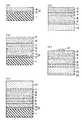
【0015】
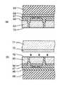
この熱膨張係数の関係によって窒化物半導体層の割れや欠けが防止できるメカニズムは、以下のように推定される。図2乃至4を参照しながら簡単に説明する。単純な例として、成長基板としてのサファイア基板22上に、GaN層23を成長し、GaN層23の上に支持基板24を接合する場合を考える。サファイアの熱膨張係数Aは、約7.5×10⁻⁶K−1であり、GaNの熱膨張係数Bは、c軸方向で約3.17×10⁻⁶K−1、a軸方向で約5.59×10⁻⁶K−1である。本件発明では、互いの接合界面の面方向における熱膨張係数の大小が問題となるため、サファイア基板のc面上にc軸成長させたGaNの場合、GaNのa軸方向での熱膨張係数に対する大小を調べれば良い。この上に種々の熱膨張係数Cを持った支持基板を形成する。
【0016】
まず、熱膨張係数の関係が「C>A>B」である場合、ウエハの反りは図2のようになる。サファイア基板22のc面上にGaN層23を形成した状態では、図2(a)に示すように、GaN層23の側が凸の反り形状となっている。そのGaN層23の上に、熱膨張係数Cがサファイア基板の熱膨張係数Aよりも大きな支持基板24を接合すると、図2(b)に示すように、反りの方向が逆転する。このとき、GaN層23には大きな歪みが加わるため、GaN層にクラックが生じたり、GaN層が剥がれるといった問題が生じ易い。
【0017】
次に、熱膨張係数の関係が「A>B>C」である場合、ウエハの反りは図3のようになる。まず、サファイア基板22のc面上にGaN層23を形成した状態では、図3(a)に示すように、GaN層23の側が凸の反り形状となっている。そのGaN層23の上に、熱膨張係数CがGaN層の熱膨張係数Bよりも小さな支持基板24を接合すると、図3(b)に示すように、反りの方向は変わらない。次に、図3(c)に示すように、ウエハを上下反転させた後、図3(d)に示すように、サファイア基板22を除去する。このとき、サファイア基板22を除去する過程で反りの方向は変わらず、サファイア基板22の側が凹状の反り形状となっている。このため、サファイア基板22を研磨によって除去しようとしても、周辺部のみ研磨が進み、均一な研磨が困難である。また、レーザ照射によってサファイア基板22を除去しようとしても、サファイア基板22がGaN層から浮上がりにくい。従って、サファイア基板22の除去が難しく、無理にサファイア基板22を除去しようとするとGaN層23に割れや剥離が生じてしまう。
【0018】
これに対し、熱膨張係数の関係が「A≧C>B」である場合、ウエハの反りは図4のようになる。まず、サファイア基板22のc面上にGaN層23を形成した状態では、図4(a)に示すように、GaN層23の側が凸の反り形状となっている。そのGaN層23の上に、熱膨張係数Cがサファイア基板22の熱膨張係数Aと同じか、やや小さな支持基板24を接合すると、図4(b)に示すように、反りが緩和される。次に、図4(c)に示すように、ウエハを上下反転させた後、図4(d)に示すように、サファイア基板22を除去する。このとき、サファイア基板22を除去すると、サファイア基板22の側が凸の反り形状に変化する。このため、サファイア基板22を研磨によって除去する際に、均一な研磨が行い易い。また、レーザ照射によってサファイア基板22を除去する場合にも、サファイア基板22がGaN層23から浮上がり易い。従って、サファイア基板22を除去する際に、GaN層23に割れや剥離が発生することを抑制できる。
【0019】
このように、成長用基板と窒化物半導体層と支持基板との3つの熱膨張係数をそれぞれA、B、Cとしたとき、「A≧C>B」とすることにより、窒化物半導体層に生じる欠けや割れを大幅に低減し、高い歩留で窒化物半導体素子を得ることが可能となる。また、上記のような熱膨張係数の関係とすることには、サファイア基板22を除去した後の工程が容易になる利点もある。即ち、図4(d)に示すように、最終的に窒化物半導体層23の側が凸の反り形状となるため、支持基板24の側を吸着する真空吸着によってフラットになり易い。従って、窒化物半導体層23の研磨工程において均一な研磨が可能となり、フォトリソグラフィ工程におけるレジストの均一な塗布が可能となる。
【0020】
尚、本発明における支持基板の熱膨張係数Cは、「A≧C>B」の関係を充たすものであれば良いが、より好ましくは、成長用基板上の窒化物半導体層の厚さに応じて熱膨張係数Cの値を調整する。即ち、窒化物半導体層の膜厚が成長用基板の膜厚に比べて十分に薄い場合(例えば、窒化物半導体層の膜厚が30μm以下の場合)、支持基板の熱膨張係数Cを成長用基板の熱膨張係数Aとほぼ同じにすることが好ましい。この場合、支持基板の熱膨張係数Cと成長用基板の熱膨張係数Aが完全に一致している必要はなく、支持基板の熱膨張係数Cが成長用基板の熱膨張係数Aの±10%程度であれば良い。一方、窒化物半導体層の膜厚が厚い場合(例えば、窒化物半導体層の膜厚が30μmを超える場合)、支持基板の好ましい熱膨張係数Cは、窒化物半導体層の膜厚に応じて、成長用基板の熱膨張係数Aから窒化物半導体層の熱膨張係数Bに近い方に変化していく。
【0021】
また、本件第1発明の製造方法では、上記第1の接合層がp型窒化物半導体層の直上に形成されたオーミック電極層を含むことが好ましい。さらに、第1の接合層が第1の共晶形成層を有し、かつ、第2の接合層が第2の共晶形成層を有することが好ましい。接合時には、第1及び第2の共晶形成層のそれぞれを構成する金属が互いに拡散して共晶を形成するので、接合力を高めることができる。
【0022】
次に、本件第2発明の製造方法は、対向する二つの主面を有する基板の一方の主面上に、少なくとも、1層以上のp型窒化物半導体層と、AlaInbGa1−a−bN(0≦a≦1、0≦b≦1、a+b≦1)から成る井戸層とAlcIndGa1−c−dN(0≦c≦1、0≦d≦1、c+d≦1)から成る障壁層とを少なくとも含む量子井戸構造を有する活性層と、1層以上のn型窒化物半導体層と、を有する窒化物半導体素子の製造方法であって、
(a)対向する二つの主面を有する成長用基板の一方の主面上に、上記活性層の発光を自己吸収する窒化物半導体を含んだ下地層を成長し、
(b)上記下地層の上に、少なくとも、前記n型窒化物半導体層と、活性層と、p型窒化物半導体層とを成長し、
(c)上記p型窒化物半導体層の上に、上記基板を接合し、
(d)上記成長用基板と上記下地層とを除去することを特徴とする。
【0023】
例えば380nm以下の紫外領域の窒化物半導体素子においては、上記成長用基板の一方の主面に接して、GaeAl1−eN(0<e≦1)から成るバッファ層と、アンドープのGaN及びn型不純物をドープしたGaNのいずれかから成る高温成長層と、を含む下地層を設けることができる。下地層はその上に成長させる窒化物半導体の結晶性を向上させる効果を有する。さらに、アンドープのGaNまたはn型不純物をドープしたGaNのいずれかから成る高温成長層は、この層を成長させることで、その上に成長させる窒化物半導体層の結晶性を大きく向上させることができる。結晶性の良い窒化物半導体素子を得るためには、成長用基板、さらにはバッファ層の上に高温でGaN層を成長させることが必要となる。この層を成長させずに活性層等を成長させても結晶性が非常に悪く、窒化物半導体発光素子などにおいては、発光出力が非常に弱く、実用的でない。
【0024】
このように、GaNからなる高温成長層を設けることで、結晶性の良い窒化物半導体素子を得ることができるが、下地層およびこの高温成長層としてGaNを含む場合、紫外領域ではGaNの自己吸収により、活性層からの光の一部がこのGaN層で吸収されてしまい、発光出力が低下してしまう。本発明においては、導電性基板を接合した後、成長用基板と下地層および高温成長層のGaNとを除去するようにしたので、素子を構成する窒化物半導体の結晶性を良好に維持しながら、自己吸収を抑制することが可能となる。
【0025】
尚、下地層を除去する際、下地層を完全に除去しなくても、発光の自己吸収を十分抑制できる程度に除去できていれば良い。例えば、上記の例において、発光を自己吸収するGaN層の膜厚が0.1μm、好ましくは0.01μmになるまで除去すれば、自己吸収を十分抑制することができる。GaN層の膜厚がが0.1μm以下に薄膜化されている場合、発光の約70%以上を取出すことができ、0.01μm以下に薄膜化されている場合、発光の96%以上を取出すことができる。成長用基板を除去するには、例えば、成長用基板の他方の主面の全面に電磁波を照射する方法を用いることができる。また、成長用基板を除去後にバッファ層及び高温成長層を除去するには、例えば、エッチングや研磨等の方法を用いることができる。
【0026】
また、本件第2発明における下地層は、GaNを含む場合に限定されない。その上に成長させるn型窒化物半導体層の結晶性を向上させるような下地層であって、活性層の発光を自己吸収する窒化物半導体を含む下地層であれば良い。例えば、GaNに少量のInやAlを添加した場合であっても、その上に形成する層に比べてInやAlの含有量が十分に少なければ、結晶性を向上させる効果が得られる。そのような下地層を介して素子構造を形成した後、成長用基板と共に下地層を除去することにより、素子を構成する窒化物半導体の結晶性を良好に維持しながら、自己吸収を抑制することができる。
【0027】
ここで、「活性層の発光を自己吸収する窒化物半導体」とは、活性層の発光波長に近いバンドギャップエネルギーを有する結果、発光の吸収が無視できないような窒化物半導体を指す。例えば、窒化物半導体のバンドギャップエネルギーが、次式で表されるように、発光ピークエネルギーよりも0.1eV大きいバンドギャップエネルギーを基準として、その基準よりも小さなバンドギャップエネルギーを持っていれば、活性層の発光を自己吸収する。
(自己吸収する窒化物半導体のバンドギャップエネルギー)≦(発光ピークエネルギー+0.1eV)
尚、窒化物半導体のバンドギャップエネルギーと組成の関係については、ボウイングパラメータを1として考えれば良い。例えば3元混晶A1−xBxCの窒化物半導体のバンドギャップエネルギーは、2元混晶ACとBCのバンドギャップエネルギーをEG,AC、EG、BCとして、次式で表すことができる。
EG(A1−xBxC)=(1−x)EG,AC+xEG、BC−(1−x)x
【0028】
また、「n型窒化物半導体の結晶性を向上させる下地層」とは、その下地層を省略した点を除いて同一の層構成を持つ窒化物半導体素子と対比して、素子中のn型窒化物半導体の結晶性が高くなるような下地層をいう。一般に、下地層の上に成長させる層に比べて、結晶性が良好になり易い組成から成る下地層であれば、結晶性を向上させる機能を有する。窒化物半導体の場合、四元混晶よりも三元混晶、三元混晶よりも二元混晶の方が、結晶性が良好になり易い。また、同じ四元混晶同士又は三元混晶同士であれば、In組成比やAl組成比が小さい方が結晶性が良好になり易い。
【0029】
本件第1発明及び第2発明の製造方法(以下、本件発明の製造方法)は、互いに組合せても良いことは言うまでもない。本件発明の製造方法において、活性層がAlaInbGa1−a−bN(0≦a≦1、0≦b≦1、a+b≦1)から成る窒化物半導体素子に関するもので、AlInGaN系で発光する発光素子において、様々な波長の光を発光する素子に適応可能であるが、特に380nm以下の紫外領域の窒化物半導体素子においてさらに特別な効果を奏する。InAlGaNの4元混晶から成る井戸層と、少なくともAlを含む窒化物半導体から成る障壁層とを少なくとも含む量子井戸構造を有する活性層を有することにより、380nm以下の短波長領域に好適に使用可能な窒化物半導体素子を製造することができる。上記の活性層は、井戸層がInAlGaNの4元混晶から形成されているので、構成元素数を最小限にしながら結晶性の悪化を抑制することができ、かつ発光効率を高めることができる。また、障壁層に少なくともAlを含む窒化物半導体を用いることにより井戸層よりもバンドギャップエネルギーを大きくして発光波長に合わせた量子井戸構造の活性層を形成できるとともに、活性層内の結晶性を良好に保つことができる。
【0030】
本発明の製造方法では、高温成長層の上にさらに、組成傾斜層を設けても良い。この組成傾斜層は、高温成長層と、その上に成長させる窒化物半導体との格子不整合を緩和させるためのもので、高温成長層の組成から、その上に成長させる窒化物半導体層の組成へと組成比を変化させていく。たとえば高温成長層がアンドープのGaNであり、上に成長させる窒化物半導体層がAlvGa1−vNのn型クラッド層であるとき、高温成長層とn型クラッド層との間にGaNからAlvGa1−vNへとAlの混晶比を徐々に大きくしていく組成傾斜層を設ける。この組成傾斜層は特に、紫外領域で発光するLEDに有効で、非常に欠陥が少なく、結晶性の良い窒化物半導体層を積層することが可能となる。また、組成傾斜層は、n型クラッド層にAl混晶比が高い(例えば5%以上)窒化物半導体を用いた場合に有効であり、格子不整合を緩和して、結晶性の良い窒化物半導体層を積層することが可能となる。また、この組成傾斜層は、導電性を決定する不純物を傾斜して設けた変調ドープとしても良い。たとえば上に成長させる窒化物半導体層がSiドープのAlvGa1−vNである場合、組成傾斜層を、アンドープから、n型クラッド層のSi濃度へと不純物濃度を大きくしていく構造とすることで、さらに欠陥が少なく、結晶性の良い窒化物半導体層を積層することが可能となる。
【0031】
また、本発明の製造方法において、窒化物半導体素子の表面の少なくとも一部に、蛍光物質を含有するコーティング層を形成することが好ましい。
【0032】
本件第3発明に係る窒化物半導体素子は、特に380nm以下の紫外領域の窒化物半導体素子では、対向する二つの主面を有し、窒化物半導体よりも大きい熱膨張係数を有する基板と、該基板の一方の主面上に形成され、共晶層を有する接合層と、該接合層の上に形成された1層以上のp型窒化物半導体層と、該p型窒化物半導体層の上に形成され、少なくとも、AlaInbGa1−a−bN(0<a≦1、0<b≦1、a+b<1)から成る井戸層とAlcIndGa1−c−dN(0<c≦1、0≦d≦1、c+d<1)から成る障壁層とを有する活性層と、該活性層の上に形成されたAlを含む1層以上のn型窒化物半導体層と、を有することを特徴とする。ここで、接合層は、前述の第1の接合層と第2の接合層とから構成され、第1の共晶形成層と第2の共晶形成層とは互いに拡散して共晶層を形成している。
【0033】
上記基板は、導電性であることが好ましく、より好ましくは、高導電性金属と高硬度の金属とを含むことが望ましい。高導電性で熱膨張係数の大きな金属材料と、高硬度で熱膨張係数の小さな金属材料とを複合することによって、高導電性でかつ窒化物半導体層よりも熱膨張係数の大きな基板を構成することができる。高硬度で熱膨張係数の小さな金属材料として、例えば、Ag、Cu、Au、Pt等が挙げられる。高硬度で熱膨張係数の小さな金属材料として、例えば、W、Mo、Cr、Ni等が挙げられる。
【0034】
尚、高導電性で熱膨張係数の大きな金属材料と、高硬度で熱膨張係数の小さな金属材料とが相互に非固溶あるいは固溶限界の小さい場合には、これらの複合体によって基板を構成することができる。相互に非固溶あるいは固溶限界の小さい金属材料同士を複合することによって、互いに性質が大きく異なる金属材料同士を組合せることが可能となり、高導電性を持ちながら、所望の熱膨張係数を持った支持基板を構成することができる。また、高導電性で熱膨張係数の大きな金属材料とダイヤ等のセラミックス材料との複合体によって基板を構成しても良い。この構成によっても、高い導電性を持ちながら所望の熱膨張係数を持った支持基板を構成することができる。
【0035】
また、本件第4発明の窒化物半導体素子は、対向する二つの主面を有する基板と、該基板の一方の主面上に設けられた、共晶層を有する接合層と、該接合層の上に設けられた1層以上のp型窒化物半導体層と、該p型窒化物半導体層の上に設けられ、少なくとも、AlaInbGa1−a−bN(0<a≦1、0<b≦1、a+b<1)から成る井戸層とAlcIndGa1−c−dN(0<c≦1、0≦d≦1、c+d<1)から成る障壁層とを有する活性層と、該活性層の上に設けられ、前記活性層の発光を実質的に自己吸収しない窒化物半導体から成るn型窒化物半導体層と、を有することを特徴とする。
【0036】
ここで、「活性層の発光を実質的に自己吸収しない窒化物半導体」とは、波長で表したバンドギャップエネルギーが十分短波長であるか、又は、膜厚が十分薄いことにより、活性層からの発光の自己吸収を無視できるような窒化物半導体をいう。窒化物半導体が、(発光ピークエネルギー+0.1eV)よりも大きなバンドギャッエネルギーを持っていれば、その窒化物半導体による発光の自己吸収は無視できる。また、窒化物半導体中に、自己吸収が起きるようなバンドギャップエネルギ−を有する層が含まれている場合であっても、その層の膜厚が0.1μm以下、より好ましくは0.01μm以下であれば良い。
【0037】
また、本件第3発明及び第4発明の窒化物半導体素子(以下、本発明の窒化物半導体素子)、特に380nm以下の紫外領域の窒化物半導体素子では、上記のp型窒化物半導体層は、AlfGa1−fN(0<f<1)から成るp型コンタクト層を有し、そのp型コンタクト層には、導電性基板側でp型不純物濃度が高く、かつ、Alの混晶比が小さくなる組成勾配を有するものを用いることができる。この場合、組成勾配は、連続的に組成を変化させても、あるいは、不連続に段階的に組成を変化させても良い。
【0038】
また、本発明の窒化物半導体素子、特に380nm以下の紫外領域の窒化物半導体素子では、上記p型コンタクト層は少なくとも2層からなり、その2層は、導電性電極側に形成されたAlgGa1−gN(0<g<0.05)から成る第1のp型コンタクト層と、活性層側に形成されたAlhGa1−hN(0<h<0.1)から成る第2のコンタクト層とからなり、第1のコンタクト層は第2のコンタクト層より高いp型不純物濃度を有するものを用いることができる。しかしながら、p型コンタクト層は、必ずしもAlfGa1−fN(0<f<1)である必要はなく、GaNでもよい。これはp型コンタクト層はp電極を形成するための層であり、p電極とオーミック性が得られれば良く、厚膜で形成する高温成長層と比較して膜厚は薄くても良いからであり、p型コンタクト層にGaNを用いても、この層における自己吸収による光取り出し効率の低下はそれほど大きいものではないからである。
【0039】
本発明の素子、特に発光素子において、導電性基板と接合させて形成された窒化物半導体素子に、活性層のAlaInbGa1−a−bN(0≦a≦1、0≦b≦1、a+b≦1)からの光の一部もしくは全部を吸収して異なる波長の光を発光する蛍光物質が含有されたコーティング層を形成することで、様々な波長の光を発光することができる。特にYAGを含有させることで、白色光を発光することができ、照明用光源など用途も格段に広がる。
【0040】
また、光の一部もしくは全部を吸収して異なる波長の光を発光する蛍光物質について、可視光を吸収して異なる光を発する材料は限られており、材料の選択性に問題がある。しかしながら、紫外光を吸収して異なる光を発する材料は非常に多く、様々な用途に応じてその材料を選択することができる。材料が選択できる要因の一つとしては、紫外光で吸収する蛍光物質は光の変換効率が可視光の変換効率と比べて高いということである。特に白色光においては、演色性の高い白色光を得るなど、可能性はさらに広がる。本発明は、紫外領域で発光する窒化物半導体素子において、自己吸収の少ない窒化物半導体発光素子が得られ、さらに蛍光物質をコーティングすることで、非常に変換効率の高い白色の発光素子を得ることができる。
【0041】
【発明の実施の形態】
以下、図面を参照して本発明の実施の形態について説明する。
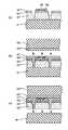
図1は、本発明に係る窒化物半導体発光素子の製造方法における製造工程の一例を示す模式断面図である。成長用基板1の表面に、バッファ層3と高温成長層4とから成る下地層2を形成する(図1(a))。次に、下地層2上にn型クラッド層5、活性層6、p型クラッド層7、p型コンタクト層8、そして、1層以上の金属層から成る第1の接合層9を形成する(図1(b))。ここで、第1の接合層9において、p型コンタクト層8上にp電極を形成した後、オーミック接触を得るためのアニール処理を行う。次に、1層以上の金属層から成る第2の接合層11を表面に形成した導電性基板10を、第1の接合層9と第2の接合層11とが対向するように成長用基板1の上に積層し、加熱圧接して接合する。
【0042】
次に、導電性基板10と接合した成長用基板1を研磨器に設置し、成長用基板1のラッピングを行い、成長用基板1と下地層2を除去して、n型クラッド層5を露出させる(図1(d))。
【0043】
次に、露出させたn型クラッド層5の表面をポリシングした後、n型クラッド層5上にn電極12を形成する一方、導電性基板10上にはp電極用パッド電極13を全面に形成する。次に、ダイシングにより発光素子をチップ状に分離する。これにより、導電性基板上に窒化物半導体層が積層され、電極が導電性基板上に形成された発光素子を得ることができる(図1(e))。
【0044】
本発明の方法において、成長用基板には、C面、R面及びA面のいずれかを主面とするサファイヤ、スピネル(MgAl2O4のような絶縁性基板)、SiC、Si、そして窒化物半導体と格子整合する酸化物基板等を挙げることができる。サファイヤやスピネルが好ましい。
【0045】
また、成長用基板上に窒化物半導体層を積層する場合、下地層上にELOG(Epitaxially Lateral Overgrowth)成長させることにより結晶性の向上した窒化物半導体を得ることができる。具体的には、成長用基板上に下地層を成長させ、その下地層上にストライプ状のマスクを複数形成し、マスクの開口部から窒化物半導体を選択成長させ、横方向の成長を伴った成長により成膜された窒化物半導体層(横方向成長層)を形成する。この横方向成長層は貫通転位が低減されているので、横方向成長層の上に形成する窒化物半導体の結晶性を向上させることができる。
【0046】
成長用基板としては、成長用基板となる材料の主面をオフアングルさせた基板、さらにステップ状にオフアングルさせた基板を用いるほうが好ましい。オフアングルさせた基板を用いると、表面の3次元成長が見られず、ステップ成長があらわれ表面が平坦になり易い。さらに、ステップ状にオフアングルされているサファイヤ基板のステップに沿う方向(段差方向)が、サファイヤのA面に対して垂直に形成されていると、窒化物半導体のステップ面がレーザの共振器方向と一致し、レーザ光が表面粗さにより乱反射されることが少なくなり好ましい。
【0047】
また、p型窒化物半導体層に接合する支持基板には、例えば、Si、SiC等の半導体から成る半導体基板、又は、金属単体基板、又は相互に非固溶あるいは固溶限界の小さい2種以上の金属の複合体から成る金属基板を用いることができる。金属基板を用いることが好ましい。金属基板は、半導体基板に比べ機械的特性が優れており、弾性変形、さらには塑性変形し易く、割れにくいからである。さらに、金属基板には、Ag,Cu,Au,Pt等の高導電性金属から選択された1種以上の金属と、W,Mo,Cr,Ni等の高硬度の金属から選択された1種以上の金属と、から成るものを用いることができる。さらに、金属基板としては、Cu−WあるいはCu−Moの複合体を用いることが好ましい。熱伝導率の高いCuを有し放熱性が優れているからである。さらに、Cu−Wの複合体の場合、Cuの含有率xが0<x≦30重量%、Cu−Moの複合体の場合、Cuの含有率xが0<x≦50重量%であることが好ましい。また、Cu−ダイヤ等の金属とセラミックスの複合体などを用いることができる。なお、p型窒化物半導体層に接合する基板の厚さは、放熱性を高めるため50〜500μmが好ましい。前記範囲に支持基板を薄くすることで放熱性が良くなる。また、支持基板には、窒化物半導体との張り合わせ面、又はその反対面に凹凸を有する構造としてもよい。
【0048】
支持基板の材料は、成長用基板と窒化物半導体層と支持基板との3つの熱膨張係数をそれぞれA、B、Cとしたとき、「A≧C>B」となるように選択することが好ましい。支持基板が金属複合体である場合には、複合する金属材料の組成比を制御することによって所望の熱膨張係数にすることができる。例えば、CuとMoとの複合体によって支持基板を構成する場合を考える。Cuの熱膨張係数は、約16×10−6K−1であり、Moの熱膨張係数は約5×10⁻⁶K−1である。従って、支持基板の熱膨張係数を小さくしたい場合には、複合体中のCu組成比を小さくし、熱膨張係数を大きくしたい場合には、Cu組成比を大きくすれば良い。
【0049】
また、第1の接合層は、少なくとも、p型窒化物半導体層とオーミック接触し、高い反射率を有するp電極をp型窒化物半導体層に接して有することが好ましい。p電極には、Ag、Rh、Ni、Au、Pd、Ir、Ti、Pt、W、Alから成る群から選択される少なくとも1種を含む金属材料を用いることが好ましい。より好ましくは、Rh,Ag,Ni−Au,Ni−Au−RhO及びRh−Irのいずれか、より好ましくは、Rhを用いることができる。ここで、p電極は、n型窒化物半導体層に比べ抵抗率の高いp型窒化物半導体層上に形成するため、p型窒化物半導体層のほぼ全面に形成することが好ましい。なお、p電極の厚さは、0.05〜0.5μmが好ましい。
【0050】
また、第1の接合層のp電極を形成したp型窒化物半導体層の露出面に絶縁性の保護膜を形成することが好ましい。この保護膜の材料には、SiO2、Al2O3、ZrO2、TiO2等から成る単層膜あるいは多層膜を用いることができる。さらに、その保護膜の上にAl、Ag、Rh等の高反射率の金属膜を形成しても良い。この金属膜により反射率が高くなり、光の取出し効率を向上させることができる。
【0051】
また、第1の接合層のp電極の上に第1の共晶形成層を設けるとともに、第2の接合層に、導電性基板の主面の上に第2の共晶形成層を設けることが好ましい。第1及び第2の共晶形成層は、接合時に互いに拡散して共晶を形成する層であり、それぞれ、Au、Sn、Pd、In、Ti、Ni、W、Mo、Au−Sn、Sn−Pd、In−Pd、Ti−Pt−Au、Ti−Pt−Sn等を用いることが好ましい。より好ましくは、第1及び第2の共晶形成層は、Au、Sn、Pd、In等の金属から成る。第1及び第2の共晶形成層の組合せは、Au−Sn、Sn−Pd、又はIn−Pdが好ましい。さらに好ましくは、第1の共晶形成層にSnを、そして第2の共晶形成層にAuを用いる組合せである。
【0052】
また、第1の接合層の第1の共晶形成層とp電極との間に、p電極側から密着層とバリア層を設けることが好ましい。密着層はp電極との間に高い密着性を確保する層であり、Ti、Ni、W及びMoのいずれかの金属が好ましい。また、バリア層は、第1の共晶形成層を構成する金属が密着層へ拡散するのを防止する層であり、PtあるいはWが好ましい。また、第1の共晶形成層の金属が密着層へ拡散するのをさらに防止するため、バリア層と第1の共晶形成層との間に、0.3μm程度の厚さのAu膜を形成しても良い。なお、第2の共晶層と導電性基板との間に、上記の密着層とバリア層及びAu膜を設けることが好ましい。
【0053】
密着層、バリア層、共晶層の組合せとして、例えばTi−Pt−Au、Ti−Pt−Sn、Ti−Pt−Pd又はTi−Pt−AuSn、W−Pt−Sn、RhO−Pt−Sn、RhO−Pt−Au、RhO−Pt−(Au、Sn)等を用いることができる。これらの金属膜は共晶により合金化され、後工程で導電層となる。また、第1の共晶層と第2の共晶層は異なることが好ましい。この理由は低温で共晶が可能で、共晶後の融点が上がるためである。
【0054】
また、接合用積層体と導電性基板とを加熱圧接する際の温度は、150℃〜350℃が好ましい。150℃以上とすることにより、共晶形成層の金属の拡散が促進され均一な密度分布の共晶が形成され、接合用積層体と導電性基板との密着性を向上させることができる。350℃より大きいと、共晶形成層の金属がバリア層、さらには密着層まで拡散して、良好な密着性が得られないからである。
【0055】
貼り合わせ時には、第1の接合層は、次のような構成となる。p電極/Ti―Pt―AuSn―Pt―Ti/導電性基板、p電極/RhO−Pt−AuSn―Pt―Ti/導電性基板、p電極/Ti―Pt―PdSn―Pt―Ti/導電性基板、p電極/Ti―Pt―AuSn―Pt―RhO/導電性基板等である。これにより剥がれにくい合金形成ができる。導電層を共晶とすることで低温での貼り合わせが可能となり、また接着力も強力になる。低温で貼り合わせることで反りの緩和効果を有する。
【0056】
また、導電性基板を接合後に成長用基板を除去するには、研磨、エッチング、電磁波照射、あるいはこれらの方法を組合せた方法を用いることができる。電磁波照射は、電磁波に例えばレーザを用い、導電性基板を接合後、成長用基板の下地層の形成されていない面の全面にレーザを照射して、下地層を分解させることにより成長用基板と下地層とを除去することができる。さらに、成長用基板と下地層とを除去した後、露出した窒化物半導体層の表面をCMP処理して所望の膜を露出させる。これにより、ダメージ層の除去や、窒化物半導体層の厚み及び表面粗さの調整を行うことができる。
【0057】
なお、電磁波照射には、以下の方法を用いることもできる。すなわち、成長用基板上に窒化物半導体からなる下地層を形成し、次いで、その下地層を部分的に成長用基板までエッチングして凹凸を形成した後、凹凸を有する下地層上にELOG成長させて横方向成長層を形成する。次いで、横方向成長層の上にn型窒化物半導体層、活性層、p型窒化物半導体層を順次形成した後、p型窒化物半導体層の上に導電性基板を接合する。次いで、成長用基板の下地層の形成されていない面の全面にレーザを照射して、下地層を分解させることにより成長用基板と下地層とを除去することができる。この方法によれば、電磁波照射時に窒化物半導体の分解により発生するN2ガスが上記の凹凸と横方向成長層との間に形成された空隙に広がり、ガス圧による成長用基板の割れを防止し、さらにその割れに起因する下地層のえぐれ傷を防止して、面状態及び結晶性の良好な窒化物半導体基板を得ることができる。また、研磨による方法に比べ、作業工程を簡略化することができるので、歩留まりが向上するという効果も得られる。
【0058】
また、成長用基板を除去した後、光の取出し効率を向上させるため、図15に示すように、n型窒化物半導体層5の露出面をRIEにより凹凸(ディンプル加工)を形成しても良い。凹凸(ディンプル加工)形成部は、窒化物半導体の光取り出し側となる。この表面の凹凸形成により光の全反射で出てこない光りを凹凸面で光の角度が変わることで取り出すことができる。即ち、発光した光を凹凸部で乱反射させることにより、従来は全反射していた光を上方へ導き、素子外部に取出すことができる。この凹凸形成は凹凸無しに比べて1.5倍以上の出力向上が期待できる。凹凸の平面形状は、丸状、または六角形や三角形の多角形状であることが好ましい。また、凹凸の平面形状を、ストライプ形状、格子形状、矩形等で形成してもよい。光の取り出し効率を上げるためには、凹凸がのパターンピッチができるだけ細かいことが好ましい。また、凹凸の断面形状は、フラットな直線で構成されているよりも、なだらかな波状であることが好ましい。凹凸の断面形状を波状とすることにより、凹凸の断面形状が角張った場合に比べて、光取り出し効率が上がる。さらに、凹部の深さは、0.2〜3μmであることが好ましく、より好ましくは1.0μm〜1.5μmである。凹部の深さが浅すぎると光取り出し向上の効果が薄れ、深すぎると横方向の抵抗が上がるためである。さらに、凹部の形状を、丸状や多角形状として抜き取った場合には、低抵抗値を維持して出力を向上させることができる。
【0059】
また、n型窒化物半導体層の露出面に形成するn電極には、Ti−Al−Ni−AuあるいはW−Al−W−Pt−Auの多層電極を用いることができる。n電極の厚さは、0.1〜1.5μmが好ましい。また、n電極以外の露出面を覆うように、SiO2、Al2O3、ZrO2、TiO2等の絶縁性の保護膜を設けることが好ましい。
【0060】
なお、p電極とn電極は、窒化物半導体素子の一方の主面にp電極が、他方の主面にn電極が形成されている限り、大きさや形状は特に限定されない。好ましくは、両電極が窒化物半導体層の積層方向から見て、互いに重ならないように対向配置されている。これにより、フェイスダウン構造の場合、発光した光を、n電極により遮られることなく効率良く取出すことができる。例えば、p電極をp型窒化物半導体層の概ね全面に形成した場合、n電極を、n型窒化物半導体層の隅部の2つ又は4つに形成しても良く、格子状に全面に形成しても良く、さらには、隅部に格子状に形成することもできる。
【0061】
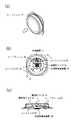
図5を参照しながら、p電極とn電極の好ましい形状について詳細に説明する。図5(a)及び(b)は、本件発明に係る窒化物半導体発光素子を示す平面図及び断面図である。支持基板10上に、第1接合層と第2接合層が共晶して形成された導電層15、p電極16、窒化物半導体17を順に設けられている。窒化物半導体17の上にはn電極12が設けられている。n電極12は、チップの対角線上の隅部にパッド電極形成領域12aを有し、パッド電極形成領域12aの間に、網目状に広がっている。n電極12を網目状、格子状等で発光範囲のほぼ全面に形成することにより、窒化物半導体層17に均一に電流を流すことができる。パッド電極形成領域12aは、対角上の2カ所に限らず、四隅全てに形成してもよい。また、p電極16とn電極12は、チップ上面から見て、互いに重ならないように形成されている。また、n電極12上には保護膜19が形成されている。保護膜19は、n電極のパッド電極形成領域12a以外であれば、窒化物半導体層17上だけでなく、p電極16上にも形成してもよい。
【0062】
図5(b)に示すように、窒化物半導体17と接しているp電極16には開口部が設けられ、その開口部内には絶縁性の保護膜20が形成されている。この保護膜20の材料には、SiO2、Al2O3、ZrO2、TiO2などの単層膜または多層膜を用いることができる。絶縁性である保護膜20を備えることにより、ショート等を防ぎ、歩留まりや信頼性を向上することができる。また、保護膜20は、反射膜(図示されていない)との2層構造であるのが好ましい。例えば、保護膜20の窒化物半導体17と接していない側に、Al、Ag、Rh等の反射膜(図示されていない)を500Å以上2000Å以下の膜厚で形成することにより、横方向に伝播する光を効率良く取り出せる。反射膜は、支持基板10側にあっても良いし、窒化物半導体17側にあっても良い。
【0063】
尚、p電極16と素子外部との電気接続は、導電層15を介して行うことができる。例えば、支持基板10が導電性である場合は、支持基板10の裏面にワイヤを接続することにより、導電層15と支持基板10を通じてp電極16と外部を電気接続することができる。支持基板10が導電性でない場合は、例えば、チップ側面から導電層15にワイヤを接続することにより、p電極16と外部を電気接続することができる。また、支持基板10と導電層15を窒化物半導体層17よりも広面積に形成しておき、窒化物半導体層17に覆われていない部分の導電層15にワイヤを接続しても良い。
【0064】
以下、本発明に係る窒化物半導体素子の具体的構成について説明する。
(下地層)
下地層2は、少なくとも1層以上の窒化物半導体で構成することができるが、成長用基板1上に低温成長させたバッファ層3と、そのバッファ層3上に高温成長させた高温成長層4とで構成することが好ましい。
【0065】
バッファ層3としては、GaiAl1−iN(0<i≦1)からなる窒化物半導体であり、好ましくはAlの割合が小さいもの、より好ましくはGaNを用いることによりバッファ層上に成長させる窒化物半導体の結晶性が向上する。バッファ層の膜厚は、好ましくは0.002〜0.5μm、より好ましくは0.005〜0.2μm、さらに好ましくは0.01〜0.02μmである。バッファ層の成長温度は、好ましくは200〜900℃、より好ましくは400〜800℃である。
【0066】
高温成長層4としては、アンドープのGaN又はn型不純物をドープしたGaNを用いることが好ましい。一般にGaNは結晶性が良好であるため、下地層としてGaNを成長させることにより、その上に成長する素子構造の結晶性も改善される。但し、高温成長層4は、結晶性改善効果を失わない程度にInやAlを含んでいても良い。高温成長層4のIn比率は、0.01以下とすることが望ましい。また、高温成長層4のAl比率は0.01以下とすることが望ましい。特に、高温成長層4にInを含んだ場合、高温成長層4の結晶性が柔らかくなり、成長用基板との界面で発生した歪みを緩和する効果も得られる。高温成長層の膜厚は、500Å以上、より好ましくは5μm以上、さらに好ましくは10μm以上である。また、高温成長層の成長温度は、900〜1100℃、好ましくは1050℃以上である。
【0067】
また、高温成長層4に用いる窒化物半導体が活性層からの発光を自己吸収する場合には、高温成長層4を最終的に除去することが好ましい。例えば、高温成長層4のバンドギャップエネルギーが、(発光ピークエネルギー+0.1eV)よりも小さな場合、高温成長層4によって活性層からの発光が吸収されてしまうため、そのような高温成長層4を除去することによって、発光強度を高めることができる。尚、発光の自己吸収が問題にならない程度の膜厚、例えば、0.1μm以下(より好ましくは0.01μm)の膜厚であれば、高温成長層4の一部を残しても良い。
【0068】
(n型クラッド層、兼n型コンタクト層5)
n型クラッド層5としては、活性層6のバンドギャップエネルギーより大きくなる組成であり、活性層6へのキャリア閉じ込めが可能であれば特に限定されないが、AljGa1−jN(0<j<0.3)が好ましい。ここで、さらに好ましくは、0.1<j<0.2である。n型クラッド層の膜厚は特に限定されるものではないが、好ましくは0.01〜0.1μm、より好ましくは0.03〜0.06μmである。また、n型クラッド層のn型不純物濃度は特に限定されるものではないが、好ましくは1×10¹⁷〜1×10²⁰/cm3、より好ましくは1×1018〜1×1019/cm3である。また、本発明においては、導電性基板を接合した後、成長用基板と下地層および高温成長層のGaNとを除去する場合、ある程度の膜厚が必要であり、その場合は1μm〜10μm、より好ましくは1μm〜5μmとする。尚、本実施の形態では、n型クラッド層5によってn型コンタクト層を兼用している。
【0069】
(n型コンタクト層の他の形態)
本実施の形態において、n型窒化物半導体層と良好なオーミック接触が得られる材料であればn電極として用いることができる。しかしながら、本発明のように、製造工程として、▲1▼p電極を形成する、▲2▼オーミックアニールする、▲3▼導電性基板を接合する、▲4▼成長用基板を除去する、▲5▼n電極を形成する、これらの▲1▼〜▲5▼工程が降順で行われる場合、特にn電極はオーミックアニールせずに設けられる。また、オーミックアニールをしようとしても、導電性基板の接合層内に含まれる共晶層が存在するため、高温でアニールすることは難しい。このため、n電極形成後に行われるクリーニング処理などの工程で、基板に150℃〜350℃の熱が加わり、これによりn電極が熱的に不安定になるという問題がある。またこの製造工程で形成された高出力の発光素子においては、発光時の熱によって、n電極が熱的に不安定になるという問題がある。さらにはこの熱的不安定によって、ショットキー接触になってしまう傾向がある。
【0070】
また本発明の構成においては、成長用基板側を除去することでn型窒化物半導体層を露出し、その露出面にn電極を形成するため、露出された面は研磨などによる微小なクラックの発生が見られる傾向にある。このクラックの発生は通電時に均一に電流を流すことの妨げになるほか、n電極とn型窒化物半導体層との密着特性(接着強度)が再現性よく得られなくなってしまう。
【0071】
さらに、本実施の形態では、活性層の発光を自己吸収する下地層を成長用基板と共に除去するため、n電極を形成するコンタクト層(本実施の形態ではn型クラッド層)のバンドギャップエネルギーは従来の窒化物半導体発光素子に比べて大きくなる。ところが、一般に半導体材料のバンドギャップエネルギーが大きくなる程、オーミック接触が取り難くなる傾向にある。
【0072】
これらの問題を解決する好ましい形態として、本発明の窒化物半導体素子は、n型窒化物半導体層に接するn電極を有し、該n型窒化物半導体層は、n電極と接する層としてn型不純物をドープした第1のn型窒化物半導体層と、前記第1のn型窒化物半導体層より活性層側に、アンドープの第2のn型窒化物半導体層、もしくは第1のn型窒化物半導体層のドープ量よりも少ないn型不純物をドープした第2のn型窒化物半導体層の、少なくとも2層を有する。例えば、図10に示すように、n型コンタクト層を兼用しているn型クラッド層5を、第1のn型窒化物半導体層5aと第2のn型窒化物半導体層5bに分ける。
【0073】
それぞれの好ましいn型不純物ドープ量としては、第1のn型窒化物半導体層5aが3×10¹⁸/cm3以上、1×1020/cm3以下、第2のn型窒化物半導体層5bが1×1017/cm3以上、3×1018/cm3未満、もしくはアンドープである。それぞれのn型窒化物半導体層は同一組成でも異なっていても良いが、上記n型クラッド層5に好ましい組成として記載した範囲で形成することが好ましい。
【0074】
活性層に近い第2のn型窒化物半導体層5bのn型不純物濃度を小さくするのは、n型不純物が活性層に悪影響を与えることを避けるためである。本件発明においては、導電性の支持基板を接合する際に加熱圧接を行い、n型窒化物半導体層の一部を研磨やレーザ照射で除去する等、特有の工程を経るため、活性層に近いn型窒化物半導体層にn型不純物が多く含まれていると活性層に悪影響を及ぼす。そこで、n電極を形成する第1のn型窒化物半導体層5aはn型不純物を高濃度でドープする一方、活性層に近い第2のn型窒化物半導体層5bのn型不純物濃度を下げることにより、特性の優れた窒化物半導体素子を構成することができる。
【0075】
第1のn型窒化物半導体層5aの膜厚は、成長用基板と下地層および高温成長層のGaNとを除去するので、ある程度の膜厚が必要で、1.5μm〜10μm、より好ましくは1μm〜5μmとする。特に研磨による精度が±0.5μmであるため、少なくとも1μm以上は必要である。第2のn型窒化物半導体層5bの膜厚は、成長用基板が除去されるとき及び第1の窒化物半導体層が露出されるときの機械的衝撃を緩和し、活性層が良好な発光特性を維持できる程度の膜厚が必要で、好ましくは0.1μm以上、1.5μm以下とする。また第2の窒化物半導体層5bは、第1の窒化物半導体層5aが高濃度で不純物がドープされていることによる結晶性の低下を回復する機能も有する。また、第1のn型窒化物半導体層5aと第2のn型窒化物半導体層5bとを含むn型窒化物半導体層の総膜厚は、p型窒化物半導体層の総膜厚よりも大きいことが好ましく、これによりn電極は、活性層からみて導電性基板側に有するp電極よりも活性層からの距離が離れているため、発光による熱的影響も受けにくくなる。
【0076】
(活性層)
本発明に用いる活性層6は、少なくとも、AlaInbGa1−a−bN(0≦a≦1、0≦b≦1、a+b≦1)から成る井戸層と、AlcIndGa1−c−dN(0≦c≦1、0≦d≦1、c+d≦1)から成る障壁層と、を含む量子井戸構造を有する。さらに好ましくは、上記井戸層及び障壁層が、それぞれ、AlaInbGa1−a−bN(0<a≦1、0<b≦1、a+b<1)と、AlcIndGa1−c−dN(0<c≦1、0≦d≦1、c+d<1)である。また、活性層における波長は380nm以下であることが好ましく、具体的には井戸層のバンドギャップエネルギーが波長380nm以下のものであることが好ましい。
【0077】
活性層に用いられる窒化物半導体は、ノンドープ、n型不純物ドープ、p型不純物ドープのいずれでも良いが、好ましくは、ノンドープもしくはアンドープ、又はn型不純物ドープの窒化物半導体を用いることにより発光素子を高出力化することができる。さらに好ましくは、井戸層をアンドープとし、障壁層をn型不純物ドープとすることで、発光素子の出力と発光効率を高めることができる。
【0078】
ここで、量子井戸構造としては、多重量子井戸構造、単一量子井戸構造のどちらでも良い。好ましくは、多重量子井戸構造とすることで、出力の向上、及び発振閾値の低下を図ることができる。
【0079】
[井戸層]
本発明の発光素子に用いる井戸層には、p型不純物又はn型不純物がドープされていても、アンドープでも良いが、n型不純物で好ましい。発光効率を向上させるからである。一方、AlInGaNの4元混晶では不純物濃度が大きくなると結晶性が低下するため、結晶性の良好な井戸層を形成するためには不純物濃度は低く抑える必要がある。具体的には、結晶性を最大限に良好なものとするためには井戸層をアンドープで成長させることであり、この場合、不純物濃度は5×10¹⁶/cm3以下と実質的に不純物を含まない井戸層とすることが好ましい。
【0080】
また、n型不純物をドープする場合、n型不純物濃度が1×10¹⁸/cm3以下5×1016/cm3以上の範囲でドープすることが好ましい。n型不純物濃度がこの範囲内であれば、結晶性の悪化を抑えながらキャリア濃度を高くすることができるので、閾値電流密度やVfを低下させることができる。また、井戸層にn型不純物をドープする場合、井戸層のn型不純物濃度を障壁層のn型不純物濃度とほぼ同じあるいは小さくすることが好ましい。井戸層での発光再結合を促し、発光出力が向上するからである。また、井戸層と障壁層をアンドープで成長させることもできる。また、多重量子井戸構造の場合、複数の井戸層の不純物濃度は必ずしも同一であることを要しない。
【0081】
なお、高出力のLDやハイパワーLEDなど、大電流で素子を駆動させる高出力素子の場合、井戸層がアンドープで実質的にn型不純物を含有しないと、井戸層でのキャリアの再結合が促進されて高い効率での発光再結合が実現される。一方、n型不純物を井戸層にドープすると、井戸層のキャリア密度が高くなり発光再結合の確率が減少し、これにより一定出力下で駆動電流の上昇を招く悪循環が発生し、素子寿命が低下する。したがって、高出力素子では、井戸層のn型不純物濃度を、少なくとも1×10¹⁸/cm3以下、好ましくはアンドープ又は実質的にn型不純物を含有しない濃度とするのが好ましい。これにより、高出力で安定した駆動が可能な発光素子が得られる。
【0082】
以下の、発明の実施の形態に示す井戸層の構成は、波長380nm以下の発光・発振が可能なバンドギャップエネルギーを有するものに好ましい構成である。
【0083】
本発明の発光素子に用いる井戸層は、従来のInGaNの井戸層では困難な波長域、具体的には、GaNのバンドギャップエネルギーである波長365nm付近、もしくはそれより短い波長を得るものであり、特に波長380nm以下の発光・発振が可能なバンドギャップエネルギーを有するものである。従来のInGaNの井戸層の場合、GaNのバンドギャップエネルギーである波長365nm付近、例えば、波長370nmを得ようとすると、In組成比を1%以下程度に調製する必要がある。しかし、このようにIn組成比が極端に小さくなると、発光効率が低下して十分な出力の発光素子が得ることができず、また成長を制御するのも困難である。本発明ではAlとInを含む窒化物半導体からなる井戸層を用い、Al組成比を大きくしてバンドギャップエネルギーを大きくし、かつInを含有させることにより、従来効率的な発光が困難であった380nmの波長域においても、良好な内部量子効率や発光効率を有する発光素子を得ることができる。
【0084】
ここで、井戸層に用いられるInAlGaNの4元混晶におけるIn組成比bは、好ましくは0.02以上0.1以下、より好ましくは0.03以上0.05以下である。In組成比bの下限を0.02以上とすることにより0.02未満の場合に比べ良好な発光効率と内部量子効率が得られ、さらに0.03以上とすることでその効率が向上する。また、上限を0.1以下とすることでInを含有することによる結晶性の悪化を抑制し、さらに0.05以下とすることで結晶性の悪化を抑制して井戸層を形成することができるので、多重量子井戸構造のように複数の井戸層を設ける場合に各井戸層の結晶性を良好なものとすることができる。
【0085】
また、井戸層に用いられるInAlGaNの4元混晶におけるAl組成比aは、良好な発光及び発振を得るためには、波長380nm以下となるバンドギャップエネルギーを設ける場合には0.02以上、さらにGaNのバンドギャップエネルギーである波長365nm以下の場合には0.05以上が好ましい。
【0086】
また、井戸層の膜厚は、好ましくは1nm以上30nm以下、より好ましくは2nm以上20nm以下、さらに好ましくは3.5nm以上20nm以下である。1nmより小さいと井戸層として良好に機能せず、30nmより大きいとInAlGaNの4元混晶の結晶性が低下し素子特性が低下するからである。また、2nm以上では膜厚に大きなむらがなく比較的均一な膜質の層が得られ、20nm以下では結晶欠陥の発生を抑制して結晶成長が可能となる。さらに膜厚を3.5nm以上とすることで出力を向上させることができる。これは井戸層の膜厚を大きくすることで、大電流で駆動させるLDのように多数のキャリア注入に対して、高い発光効率及び内部量子効率により発光再結合がなされるものであり、特に多重量子井戸構造において効果を有する。また、単一量子井戸構造では膜厚を5nm以上とすることで上記と同様に出力を向上させる効果が得られる。
【0087】
また特に井戸層InGaNのIn混晶比が0.01以下においては、井戸層の膜厚を10nm以上、障壁層をAlcGa1−cN(0<c<1)の範囲にすることによって、370nm以下での良好な発光効率の発光素子を得ることも可能である。
【0088】
[障壁層]
量子井戸構造の活性層において、障壁層を井戸層と交互に形成しても良く、1つの井戸層に対して複数の障壁層を設けても良い。例えば、井戸層に挟まれた障壁層を2層以上とし、多層膜の障壁層と井戸層とを交互に積層した構造とすることができる。
【0089】
また、障壁層は、井戸層の場合と同様に、好ましくはp型不純物又はn型不純物がドープされているか又はアンドープであること、より好ましくはn型不純物がドープされているか又はアンドープであることである。例えば、障壁層中にn型不純物をドープする場合、その濃度は少なくとも5×10¹⁶/cm3以上が必要である。例えば、LEDでは、5×1016/cm3以上2×1018/cm3以下が好ましい。また、高出力のLEDやLDでは、5×1017/cm3以上1×1020/cm3以下、より好ましくは1×1018/cm3以上5×1019/cm3以下である。この場合、井戸層はn型不純物を実質的に含有しないか、あるいはアンドープで成長させることが好ましい。
【0090】
また、障壁層にn型不純物をドープする場合、活性層内のすべての障壁層にドープしても良く、あるいは、一部をドープとし一部をアンドープとすることもできる。ここで、一部の障壁層にn型不純物をドープする場合、活性層内でn型層側に配置された障壁層にドープすることが好ましい。例えば、n型層側から数えてn番面の障壁層Bn(nは正の整数)にドープすることで、電子が効率的に活性層内に注入され、優れた発光効率と内部量子効率を有する発光素子が得られる。また、井戸層についても、n型層側から数えてm番目の井戸層Wm(mは正の整数)にドープすることにより上記の障壁層の場合と同様の効果が得られる。また、障壁層と井戸層の両方にドープしても同様の効果が得られる。
【0091】
以下の、発明の実施の形態に示す障壁層の構成は、波長380nm以下の発光・発振が可能なバンドギャップエネルギーを有するものに好ましい構成である。
【0092】
本発明の発光素子においては、障壁層は井戸層よりもバンドギャップエネルギーの大きな窒化物半導体を用いる必要がある。特に、井戸層の発光波長が380nm以下の領域では、障壁層には一般式AlcIndGa1−c−dN(0<c≦1、0≦d≦1、c+d<1)で表わされるAlInGaNの4元混晶、又はAlGaNの3元混晶を用いることが好ましい。障壁層のAl組成比cは、井戸層のAl組成比aよりも大きく、c>aとして、井戸層と障壁層との間に十分なバンドギャップエネルギーを設けることで、発光素子として良好な発光効率を有する量子井戸構造を形成することができる。また、障壁層がInを含有する場合(d>0)、In組成比dは0.1以下、より好ましくは0.05以下である。In組成比dが0.1を超えると、成長時にAlとInとの反応が促進され結晶性が悪化して良好な膜が形成されないためである。In組成比dを0.05以下とすることにより、さらに結晶性を向上させて良好な膜を形成することができる。
【0093】
また、主にAl組成比によりバンドギャップエネルギーの差を設けること、そして障壁層のIn組成比dは井戸層のIn組成比bに比べ広い組成比を適用できることから、d≧bとすることも可能である。その場合、井戸層と障壁層の臨界膜厚を変化させることができるので、量子井戸構造において自由に膜厚を設定でき、所望の特性の活性層を設計することができる。
【0094】
障壁層の膜厚は、好ましくは井戸層の場合と同様に1nm以上30nm以下、より好ましくは2nm以上20nm以下である。1nmより小さいと均一な膜が得られず障壁層として十分に機能せず、また、30nmより大きいと結晶性が悪化するからである。
【0095】
(p型クラッド層)
p型クラッド層7としては、活性層6のバンドギャップエネルギーより大きくなる組成であり、活性層6へのキャリアの閉じ込めができるものであれば特に限定されないが、AlkGa1−kN(0≦k<1)が用いられ、特にAlkGa1−kN(0<k<0.4)が好ましい。ここで、より好ましくは、0.15<k<0.3である。p型クラッド層の膜厚は特に限定されないが、好ましくは0.01〜0.15μm、より好ましくは0.04〜0.08μmである。p型クラッド層のp型不純物濃度は、1×10¹⁸〜1×10²¹/cm3、1×1019〜5×1020cm3である。p型不純物濃度が上記の範囲にあると、結晶性を低下させることなくバルク抵抗を低下させることができる。
【0096】
p型クラッド層は、単一層でも多層膜層(超格子構造)でも良い。多層膜層の場合、上記のAlkGa1−kNと、それよりバンドギャップエネルギーの小さい窒化物半導体層とからなる多層膜層であれば良い。例えばバンドギャップエネルギーの小さい層としては、n型クラッド層の場合と同様に、InlGa1−lN(0≦l<1)、AlmGa1−mN(0≦m<1、m>l)が挙げられる。多層膜層を形成する各層の膜厚は、超格子構造の場合は、一層の膜厚が好ましくは100Å以下、より好ましくは70Å以下、さらに好ましくは10〜40Åとすることができる。また、p型クラッド層がバンドギャップエネルギーの大きい層と、バンドギャップエネルギーの小さい層からなる多層膜層である場合、バンドギャップエネルギーの大きい層及び小さい層の少なくともいずれか一方にp型不純物をドープさせても良い。また、バンドギャップエネルギーの大きい層及び小さい層の両方にドープする場合は、ドープ量は同一でも異なっても良い。
【0097】
(p型コンタクト層)
p型コンタクト層8は、AlfGa1−fN(0≦f<1)が用いられ、特に、AlfGa1−fN(0<f<0.3)で構成することによりオーミック電極9と良好なオーミックコンタクトが可能となる。p型不純物濃度は1×10¹⁷/cm3以上が好ましい。
【0098】
また、p型コンタクト層8は、導電性基板側でp型不純物濃度が高く、かつ、Alの混晶比が小さくなる組成勾配を有することが好ましい。この場合、組成勾配は、連続的に組成を変化させても、あるいは、不連続に段階的に組成を変化させても良い。例えば、p型コンタクト層8を、オーミック電極9と接し、p型不純物濃度が高くAl組成比の低い第1のp型コンタクト層と、p型不純物濃度が低くAl組成比の高い第2のp型コンタクト層とで構成することもできる。第1のp型コンタクト層により良好なオーミック接触が得られ、第2のp型コンタクト層により自己吸収を防止することが可能となる。
【0099】
第1のp型コンタクト層の組成は、AlgGa1−gN(0≦g<0.05)が好ましく、より好ましくはgが、0<g<0.01である。Al組成比が上記の範囲内であれば、p型不純物を高濃度にドープしても不純物の不活性化を防止でき、良好なオーミック接触が得られる。また、第1のp型コンタクト層のp型不純物濃度は、好ましくは1×10¹⁹〜1×10²²/cm3、より好ましくは5×1020〜5×1021/cm3である。また、第1のp型コンタクト層の膜厚は、好ましくは100〜500Å、より好ましくは150〜300Åである。
【0100】
また、第2のp型コンタクト層の組成は、AlhGa1−hN(0≦h<0.1)が好ましく、より好ましくはhが、0.1<h<0.05である。Al組成比が上記の範囲内であれば、自己吸収を防止することが可能となる。また、第2のp型コンタクト層のp型不純物濃度は、好ましくは1×10²⁰/cm3以下、より好ましくは5×1018〜5×1019/cm3である。また、第2のp型コンタクト層の膜厚は、好ましくは400〜1200Å、より好ましくは800〜1200Åである。
【0101】
(蛍光体)
[蛍光体の種類]
本発明の窒化物半導体素子、特に発光素子において、支持基板と接合させて形成された窒化物半導体素子に、活性層からの光の一部もしくは全部を吸収して異なる波長の光を発光する蛍光物質が含有されたコーティング層や封止部材を形成することで、様々な波長の光を発光することができる。蛍光物質の一例を以下に示す。緑色系発光蛍光体(以下、グループ1と称することがある)としては、SrAl2O4:Eu、Y2SiO5:Ce,Tb、MgAl11O19:Ce,Tb、Sr7Al12O25:Eu、(Mg、Ca、Sr、Baのうち少なくとも1以上)Ga2S4:Eu、BaAl12O19:Eu,Mn、ZnS:Cu,Alがある。また、青色系発光蛍光体(以下にグループ2と称することがある)としてはSr5(PO4)3Cl:Eu、(SrCaBa)5(PO4)3Cl:Eu、(BaCa)5(PO4)3Cl:Eu、(Mg、Ca、Sr、Baのうち少なくとも1以上)2B5O9Cl:Eu,Mn、(Mg、Ca、Sr、Baのうち少なくとも1以上)(PO4)6Cl2:Eu,Mn、BaAl12O19:Mn、Ca(PO4)3Cl:Eu、CaB5O9Cl:Euがある。さらに、赤色系発光蛍光体(以下にグループ3と称することがある)としてはY2O2S:Eu、La2O2S:Eu、Y2O3:Eu、Gd2O2S:Euがある。さらに、黄色系発光蛍光体(以下にグループ4と称することがある)としてはYAG、Tb3Al5O12:Ce、(BaSrCa)2SiO4:Eu、CaGaS4:Euがある。この他、青緑系発光蛍光体としてはSr4Al14O25:Eu、黄赤色系発光蛍光体としてCa2Si5N8:Eu、橙色系発光蛍光体としてはZnS:Mnがある。
【0102】
特にYAGとグループ2から選択された蛍光体とを含有させることで、白色光を発光することができ、照明用光源など用途も格段に広がる。YAGは、(Y1−xGdx)3(Al1−yGay)5O12:R(Rは、Ce、Tb、Pr、Sm、Eu、Dy、Hoから選ばれる少なくとも1以上である。0<R<0.5である。)、例えば、(Y0.8Gd0.2)3Al5O12:Ce、Y3(Al0.8Ga0.2)5O12:Ceである。
【0103】
また、光の一部もしくは全部を吸収して異なる波長の光を発光する蛍光体について、可視光を吸収して異なる光を発する材料は限られており、材料の選択性に問題がある。しかしながら、紫外光を吸収して異なる光を発する材料は非常に多く、様々な用途に応じてその材料を選択することができる。材料が選択できる要因の一つとしては、紫外光で吸収する蛍光体は光の変換効率が可視光の変換効率と比べて高いということである。特に白色光においては、演色性の高い白色光を得るなど、可能性はさらに広がる。たとえば、グループ1とグループ2とグループ3からそれぞれ選択された蛍光体を用いたり、グループ2とグループ4からそれぞれ選択された蛍光体を用いたり、青緑系発光蛍光体とグループ3からそれぞれ選択された蛍光体を用いたりすることで、白色光を得ることができる。本発明は、なかでも紫外領域で発光する窒化物半導体素子において、自己吸収の少ない窒化物半導体発光素子が得られ、さらに蛍光物質をコーティングすることで、非常に変換効率の高い白色の発光素子を得ることができる。
【0104】
[蛍光体の粒径]
本発明で用いられる蛍光体の粒径は、中心粒径が6μm〜50μmの範囲が好ましく、より好ましくは15μm〜30μmであり、このような粒径を有する蛍光体は光の吸収率及び変換効率が高く且つ励起波長の幅が広い。6μmより小さい蛍光体は、比較的凝集体を形成しやすく、液状樹脂中において密になって沈降されるため、光の透過効率を減少させてしまう他、光の吸収率及び変換効率が悪く励起波長の幅も狭い。
【0105】
本件明細書において、蛍光体の粒径とは、体積基準粒度分布曲線により得られる値であり、体積基準粒度分布曲線は、レーザ回折・散乱法により蛍光体の粒度分布を測定し得られるものである。具体的には、気温25℃、湿度70%の環境下において、濃度が0.05%であるヘキサメタリン酸ナトリウム水溶液に蛍光体を分散させ、レーザ回折式粒度分布測定装置(SALD−2000A)により、粒径範囲0.03μm〜700μmにて測定し得られたものである。また、本件明細書において蛍光体の中心粒径とは、体積基準粒度分布曲線において積算値が50%のときの粒径値である。この中心粒径値を有する蛍光体が頻度高く含有されていることが好ましく、頻度値は20%〜50%が好ましい。このように粒径のバラツキが小さい蛍光体を用いることにより、色ムラが抑制され良好なコントラストを有する発光装置が得られる。
【0106】
[イットリウム・アルミニウム酸化物系蛍光体]
本件発明に用いることができる蛍光体の中でも、窒化物系半導体を発光層とする半導体発光素子から発光された光により励起されて発光し、セリウム(Ce)あるいはプラセオジウム(Pr)で付活されたイットリウム・アルミニウム酸化物系蛍光体をベースとした蛍光体(YAG系蛍光体)は、白色系発光が可能となる点で好ましい。具体的なイットリウム・アルミニウム酸化物系蛍光体としては、YAlO3:Ce、Y3Al5O12:Ce(YAG:Ce)やY4Al2O9:Ce、更にはこれらの混合物などが挙げられる。イットリウム・アルミニウム酸化物系蛍光体にBa、Sr、Mg、Ca、Znの少なくとも一種が含有されていてもよい。また、Siを含有させることによって、結晶成長の反応を抑制し蛍光体の粒子を揃えることができる。
【0107】
本明細書において、Ceで付活されたイットリウム・アルミニウム酸化物系蛍光体は特に広義に解釈するものとし、イットリウムの一部あるいは全体を、Lu、Sc、La、Gd及びSmからなる群から選ばれる少なくとも1つの元素に置換され、あるいは、アルミニウムの一部あるいは全体をBa、Tl、Ga、Inの何れが又は両方で置換され蛍光作用を有する蛍光体を含む広い意味に使用する。
【0108】
更に詳しくは、一般式(YzGd1−z)3Al5O12:Ce(但し、0<z≦1)で示されるフォトルミネッセンス蛍光体や一般式(Re1−aSma)3Re‘5O12:Ce(但し、0≦a<1、0≦b≦1、Reは、Y、Gd、La、Scから選択される少なくとも一種、Re’は、Al、Ga、Inから選択される少なくとも一種である。)で示されるフォトルミネッセンス蛍光体である。この蛍光体は、ガーネット構造のため、熱、光及び水分に強く、励起スペクトルのピークを450nm付近にさせることができる。また、発光ピークも、580nm付近にあり700nmまですそを引くブロードな発光スペクトルを持つ。
【0109】
またフォトルミネッセンス蛍光体は、結晶中にGd(ガドリニウム)を含有することにより、460nm以上の長波長域の励起発光効率を高くすることができる。Gdの含有量の増加により、発光ピーク波長が長波長に移動し全体の発光波長も長波長側にシフトする。すなわち、赤みの強い発光色が必要な場合、Gdの置換量を多くすることで達成できる。一方、Gdが増加すると共に、青色光によるフォトルミネッセンスの発光輝度は低下する傾向にある。さらに、所望に応じてCeに加えTb、Cu、Ag、Au、Fe、Cr、Nd、Dy、Co、Ni、Ti、Euらを含有させることもできる。しかも、ガーネット構造を持ったイットリウム・アルミニウム・ガーネット系蛍光体の組成のうち、Alの一部をGaで置換することで発光波長が短波長側へ、組成のYの一部をGdで置換することで、発光波長が長波長側へシフトすることができる。
【0110】
Yの一部をGdで置換する場合、Gdへの置換を1割未満にし、且つCeの含有(置換)を0.03から1.0にすることが好ましい。Gdへの置換が2割未満では緑色成分が大きく赤色成分が少なくなるが、Ceの含有量を増やすことで赤色成分を補え、輝度を低下させることなく所望の色調を得ることができる。このような組成にすると温度特性が良好となり発光ダイオードの信頼性を向上させることができる。また、赤色成分を多く有するように調整されたフォトルミネッセンス蛍光体を使用すると、ピンク等の中間色を発光することが可能な発光装置を形成することができる。
【0111】
このようなフォトルミネッセンス蛍光体は、Y、Gd、Al、及びCe、Prの原料として酸化物、又は高温で容易に酸化物になる化合物を使用し、それらを化学量論比で十分に混合して原料を得る。又は、Y、Gd、Ce、Prの希土類元素を化学量論比で酸に溶解した溶解液を蓚酸で共沈したものを焼成して得られる共沈酸化物と、酸化アルミニウムとを混合して混合原料を得る。これにフラックスとしてフッ化バリウムやフッ化アンモニウム等のフッ化物を適量混合して坩堝に詰め、空気中1350〜1450℃の温度範囲で2〜5時間焼成して焼成品を得、つぎに焼成品を水中でボールミルして、洗浄、分離、乾燥、最後に篩を通すことで得ることができる。
【0112】
本件発明の窒化物半導体素子において、このようなフォトルミネッセンス蛍光体は、2種類以上のセリウムで付活されたイットリウム・アルミニウム・ガーネット系蛍光体や他の蛍光体を混合させてもよい。YからGdへの置換量が異なる2種類のイットリウム・アルミニウム・ガーネット系蛍光体を混合することにより、容易に所望とする色調の光を容易に実現することができる。特に、前記置換量の多い蛍光体を上記蛍光体とし、前記置換量の少なく又はゼロである蛍光体を上記中粒径蛍光体とすると、演色性および輝度の向上を同時に実現することができる。
【0113】
[窒化物系蛍光体]
本発明で使用する蛍光体には、Nを含み、かつBe、Mg、Ca、Sr、Ba、及びZnから選択された少なくとも一種の元素と、C、Si、Ge、Sn、Ti、Zr、及びHfから選択された少なくとも一種の元素とを含み、希土類元素から選択された少なくとも一種の元素で付活された窒化物系蛍光体を含有させることができる。この窒化物系蛍光体は、発光素子から出光した可視光、紫外線、あるいはYAG系蛍光体からの発光を吸収することによって励起され発光することができる。窒化物系蛍光体の中でも、Mnが添加されたSr−Ca−Si−N:Eu、Ca−Si−N:Eu、Sr−Si−N:Eu、Sr−Ca−Si−O−N:Eu、Ca−Si−O−N:Eu、Sr−Si−O−N:Eu系シリコンナイトライドが好ましい。
【0114】
この蛍光体の基本構成元素は、一般式LXSiYN(2/3X+4/3Y):Eu若しくはLXSiYOZN(2/3X+4/3Y−2/3Z):Eu(Lは、Sr、Ca、SrとCaのいずれか。)で表される。一般式中、X及びYは、X=2、Y=5又は、X=1、Y=7であることが好ましいが、任意のものも使用できる。具体的には、蛍光体の基本構成元素は、Mnが添加された(SrXCa1−X)2Si5N8:Eu、Sr2Si5N8:Eu、Ca2Si5N8:Eu、SrXCa1−XSi7N10:Eu、SrSi7N10:Eu、CaSi7N10:Euとすることが好ましい。この蛍光体の組成中に、Mg、Sr、Ca、Ba、Zn、B、Al、Cu、Mn、Cr及びNiからなる群より選ばれる少なくとも1種以上が含有されていてもよい。また、SrとCaは、所望により配合比を変えることができる。蛍光体の組成にSiを用いることにより安価で結晶性の良好な蛍光体を提供することができる。
【0115】
窒化物系蛍光体において、発光中心に希土類元素であるユウロピウム(Eu)を用いるを用いることが好ましい。ユウロピウムは、主に2価と3価のエネルギー準位を持つ。本発明の蛍光体は、母体のアルカリ土類金属系窒化ケイ素に対して、Eu2+を付活剤として用いる。Eu2+は、酸化されやすく、3価のEu2O3の組成で市販されている。しかし、市販のEu2O3では、Oの関与が大きく、良好な蛍光体が得られにくい。そのため、Eu2O3からOを、系外へ除去したものを使用することが好ましい。たとえば、ユウロピウム単体、窒化ユウロピウムを用いることが好ましい。但し、Mnを添加した場合は、その限りではない。
【0116】
添加物であるMnは、Eu2+の拡散を促進し、発光輝度、エネルギー効率、量子効率等の発光効率の向上を図る。Mnは、原料中に含有させるか、又は、製造工程中にMn単体若しくはMn化合物を含有させ、原料と共に焼成する。但し、Mnは、焼成後の基本構成元素中に含有されていないか、含有されていても当初含有量と比べて少量しか残存していない。これは、焼成工程において、Mnが飛散したためであると思われる。
【0117】
窒化物系蛍光体には、基本構成元素中に、若しくは、基本構成元素とともに、Mg、Sr、Ca、Ba、Zn、B、Al、Cu、Mn、Cr、O及びNiからなる群より選ばれる少なくとも1種以上を含有することが好ましい。これらの元素は、粒径を大きくしたり、発光輝度を高めたりする等の作用を有している。また、B、Al、Mg、Cr及びNiは、残光を抑えることができるという作用を有している。
【0118】
このような窒化物系蛍光体は、発光素子によって発光された青色光の一部を吸収して黄から赤色領域の光を発光する。窒化物系蛍光体をYAG系蛍光体と共に上記の構成を有する発光装置に使用して、発光素子により発光された青色光と、窒化物系蛍光体による黄色から赤色光とが混色により暖色系の白色に発光する発光装置が得られる。窒化物系蛍光体の他に加える蛍光体には、セリウムで付活されたイットリウム・アルミニウム酸化物蛍光体が含有されていることが好ましい。前記イットリウム・アルミニウム酸化物蛍光体を含有することにより、所望の色度に調節することができるからである。セリウムで付活されたイットリウム・アルミニウム酸化物蛍光体は、発光素子により発光された青色光の一部を吸収して黄色領域の光を発光する。ここで、発光素子により発光された青色光と、イットリウム・アルミニウム酸化物蛍光体の黄色光とが混色により青白い白色に発光する。従って、このイットリウム・アルミニウム酸化物蛍光体と赤色発光する蛍光体とを、色変換層中に一緒に混合し、発光素子により発光された青色光とを組み合わせることにより白色系の混色光を発光する発光装置を提供することができる。特に好ましいのは、色度が色度図における黒体放射の軌跡上に位置する白色の発光装置である。但し、所望の色温度の発光装置を提供するため、イットリウム・アルミニウム酸化物蛍光体の蛍光体量と、赤色発光の蛍光体量を適宜変更することもできる。この白色系の混色光を発光する発光装置は、特殊演色評価数R9の改善を図っている。従来の青色系の光を出光する発光素子とセリウムで付活されたイットリウム・アルミニウム酸化物蛍光体との組合せのみの白色に発光する発光装置は、色温度Tcp=4600K付近において特殊演色評価数R9がほぼ0に近く、赤み成分が不足していた。そのため特殊演色評価数R9を高めることが解決課題となっていたが、本発明において赤色発光の蛍光体をイットリウム・アルミニウム酸化物蛍光体と共に用いることにより、色温度Tcp=4600K付近において特殊演色評価数R9を40付近まで高めることができる。
【0119】
次に、本発明に係る蛍光体((SrXCa1−X)2Si5N8:Eu)の製造方法を説明するが、本製造方法に限定されない。上記蛍光体には、Mn、Oが含有されている。
▲1▼原料のSr、Caを粉砕する。原料のSr、Caは、単体を使用することが好ましいが、イミド化合物、アミド化合物などの化合物を使用することもできる。また原料Sr、Caには、B、Al、Cu、Mg、Mn、Al2O3などを含有するものでもよい。原料のSr、Caは、アルゴン雰囲気中、グローブボックス内で粉砕を行う。粉砕により得られたSr、Caは、平均粒径が約0.1μmから15μmであることが好ましいが、この範囲に限定されない。Sr、Caの純度は、2N以上であることが好ましいが、これに限定されない。より混合状態を良くするため、金属Ca、金属Sr、金属Euのうち少なくとも1以上を合金状態としたのち、窒化し、粉砕後、原料として用いることもできる。
【0120】
▲2▼原料のSiを粉砕する。原料のSiは、単体を使用することが好ましいが、窒化物化合物、イミド化合物、アミド化合物などを使用することもできる。例えば、Si3N4、Si(NH2)2、Mg2Siなどである。原料のSiの純度は、3N以上のものが好ましいが、Al2O3、Mg、金属ホウ化物(Co3B、Ni3B、CrB)、酸化マンガン、H3BO3、B2O3、Cu2O、CuOなどの化合物が含有されていてもよい。Siも、原料のSr、Caと同様に、アルゴン雰囲気中、若しくは、窒素雰囲気中、グローブボックス内で粉砕を行う。Si化合物の平均粒径は、約0.1μmから15μmであることが好ましい。
【0121】
▲3▼次に、原料のSr、Caを、窒素雰囲気中で窒化する。この反応式を、以下の式1および式2にそれぞれ示す。
3Sr + N2 → Sr3N2 ・・・(式1)
3Ca + N2 → Ca3N2 ・・・(式2)
Sr、Caを、窒素雰囲気中、600〜900℃、約5時間、窒化する。Sr、Caは、混合して窒化しても良いし、それぞれ個々に窒化しても良い。これにより、Sr、Caの窒化物を得ることができる。Sr、Caの窒化物は、高純度のものが好ましいが、市販のものも使用することができる。
【0122】
▲4▼原料のSiを、窒素雰囲気中で窒化する。この反応式を、以下の式3に示す。
3Si + 2N2 → Si3N4 ・・・(式3)
ケイ素Siも、窒素雰囲気中、800〜1200℃、約5時間、窒化する。これにより、窒化ケイ素を得る。本発明で使用する窒化ケイ素は、高純度のものが好ましいが、市販のものも使用することができる。
【0123】
▲5▼Sr、Ca若しくはSr−Caの窒化物を粉砕する。Sr、Ca、Sr−Caの窒化物を、アルゴン雰囲気中、若しくは、窒素雰囲気中、グローブボックス内で粉砕を行う。同様に、Siの窒化物を粉砕する。また、同様に、Euの化合物Eu2O3を粉砕する。Euの化合物として、酸化ユウロピウムを使用するが、金属ユウロピウム、窒化ユウロピウムなども使用可能である。このほか、原料のZは、イミド化合物、アミド化合物を用いることもできる。酸化ユウロピウムは、高純度のものが好ましいが、市販のものも使用することができる。粉砕後のアルカリ土類金属の窒化物、窒化ケイ素及び酸化ユウロピウムの平均粒径は、約0.1μmから15μmであることが好ましい。
【0124】
上記原料中には、Mg、Sr、Ca、Ba、Zn、B、Al、Cu、Mn、Cr、O及びNiからなる群より選ばれる少なくとも1種以上が含有されていてもよい。また、Mg、Zn、B等の上記元素を以下の混合工程において、配合量を調節して混合することもできる。これらの化合物は、単独で原料中に添加することもできるが、通常、化合物の形態で添加される。この種の化合物には、H3BO3、Cu2O3、MgCl2、MgO・CaO、Al2O3、金属ホウ化物(CrB、Mg3B2、AlB2、MnB)、B2O3、Cu2O、CuOなどがある。
【0125】
▲6▼上記粉砕を行った後、Sr、Ca、Sr−Caの窒化物、Siの窒化物、Euの化合物Eu2O3を混合し、Mnを添加する。これらの混合物は、酸化されやすいため、Ar雰囲気中、又は、窒素雰囲気中、グローブボックス内で、混合を行う。
【0126】
▲7▼最後に、Sr、Ca、Sr−Caの窒化物、Siの窒化物、Euの化合物Eu2O3の混合物をアンモニア雰囲気中で、焼成する。焼成により、Mnが添加された(SrXCa1−X)2Si5N8:Euで表される蛍光体を得ることができる。ただし、各原料の配合比率を変更することにより、目的とする蛍光体の組成を変更することができる。焼成は、管状炉、小型炉、高周波炉、メタル炉などを使用することができる。焼成温度は、1200から1700℃の範囲で焼成を行うことができるが、1400から1700℃の焼成温度が好ましい。焼成は、徐々に昇温を行い1200から1500℃で数時間焼成を行う一段階焼成を使用することが好ましいが、800から1000℃で一段階目の焼成を行い、徐々に加熱して1200から1500℃で二段階目の焼成を行う二段階焼成(多段階焼成)を使用することもできる。蛍光体の原料は、窒化ホウ素(BN)材質のるつぼ、ボートを用いて焼成を行うことが好ましい。窒化ホウ素材質のるつぼの他に、アルミナ(Al2O3)材質のるつぼを使用することもできる。
以上の製造方法を使用することにより、目的とする蛍光体を得ることが可能である。
【0127】
本実施の形態において、赤味を帯びた光を発光する蛍光体として、特に窒化物系蛍光体を使用するが、本発明においては、上述したYAG系蛍光体と赤色系の光を発光可能な蛍光体とを備える発光装置とすることも可能である。このような赤色系の光を発光可能な蛍光体は、波長が400〜600nmの光によって励起されて発光する蛍光体であり、例えば、Y2O2S:Eu、La2O2S:Eu、CaS:Eu、SrS:Eu、ZnS:Mn、ZnCdS:Ag,Al、ZnCdS:Cu,Al等が挙げられる。このようにYAG系蛍光体とともに赤色系の光を発光可能な蛍光体を使用することにより発光装置の演色性を向上させることが可能である。
【0128】
以上のようにして形成されるYAG系蛍光体、および窒化物系蛍光体に代表される赤色系の光を発光可能な蛍光体は、発光素子の側方端面において一層からなる色変換層中に二種類以上存在してもよいし、二層からなる色変換層中にそれぞれ一種類あるいは二種類以上存在してもよい。このような構成にすると、異なる種類の蛍光体からの光の混色による混色光が得られる。この場合、各蛍光体から発光される光をより良く混色しかつ色ムラを減少させるために、各蛍光体の平均粒径及び形状は類似していることが好ましい。また、窒化物系蛍光体は、YAG蛍光体により波長変換された光の一部を吸収してしまうことを考慮して、窒化系蛍光体がYAG系蛍光体より発光素子の側方端面に近い位置に配置されるように色変換層を形成することが好ましい。このように構成することによって、YAG蛍光体により波長変換された光の一部が窒化物系蛍光体に吸収されてしまうことがなくなり、YAG系蛍光体と窒化物系蛍光体とを混合して含有させた場合と比較して、両蛍光体による混色光の演色性を向上させることができる。
【0129】
(パッケージ)
本発明によって得られる半導体発光素子を、例えば、以下のようなパッケージに実装して発光デバイスとすることができる。まず、図6(a)〜(c)に示すように、窒化物半導体発光素子30をリードフレーム34を備えたヒートシンク32に実装し、半導体発光素子30からリードフレーム34に導電性ワイヤー36をボンディングする。その後、透明性ガラス38でパッケージすることで発光デバイスを形成する。
【0130】
また、図6(a)〜(c)に代えて、図7(a)〜(c)に示すパッケージを用いても良い。図7では、ヒートシンク42を有するパッケージ樹脂40を準備して、ヒートシンク42上に半導体発光素子30を形成し、半導体発光素子30からリードフレーム44に導電性ワイヤー46をボンディングする。その後、シリコーン等の封止樹脂48を前記半導体発光素子30上に塗布する。さらに、その上にレンズ49を形成して発光デバイスとする。図6及び図7に示す発光装置には、静電気から半導体発光素子30を保護するための保護装置31を備えていることが好ましい。
【0131】
尚、上記実施の形態では、サファイア基板上に成長した紫外発光の発光ダイオードに本件発明を適用した場合を中心に説明したが、本件発明はこれに限定されない。サファイア以外の成長基板に成長した場合や、青色等の紫外以外の波長を発光するダイオードにも適用できる。また、発光ダイオードに限らず、レーザダイオードにも適用することができる。
【0132】
【実施例】
実施例1.
本実施例では、発光波長が375nmの発光ダイオードに本件発明を適用し、図1(a)〜(e)に示す製造方法に従って窒化物半導体素子を作成する。
(成長用基板)
成長用基板1として、サファイヤ(C面)よりなる基板を用い、MOCVD反応容器内において水素雰囲気中、1050℃で表面のクリーニングを行った。
【0133】
(下地層2)
バッファ層3:続いて、水素雰囲気中、510℃でアンモニアとTMG(トリメチルガリウム)を用い、基板上にGaNよりなるバッファ層3を約200Åの膜厚で成長させた。
【0134】
高温成長層4:バッファ層3成長後、TMGのみを止めて、温度を1050℃まで上昇させ、1050℃になったら、原料ガスにTMG、アンモニアを用い、アンドープGaNよりなる高温成長の窒化物半導体4を5μmの膜厚で成長させた。
【0135】
(n型クラッド層5)
次に、1050℃でTMG、TMA、アンモニア、シランを用い、Siを5×10¹⁷/cm3ドープしたn型Al0.18Ga0.82Nよりなるn型クラッド層5を400Åの膜厚で形成した。
【0136】
(活性層6)
次に、温度を800℃にして、原料ガスにTMI(トリメチルインジウム)、TMG、TMAを用い、SiドープのAl0.1Ga0.9Nよりなる障壁層、その上にアンドープのIn0.03Al0.02Ga0.95Nよりなる井戸層を、障壁層▲1▼/井戸層▲1▼/障壁層▲2▼/井戸層▲2▼/障壁層▲3▼の順に積層した。この時、障壁層▲1▼を200Å、障壁層▲2▼と▲3▼を40Å、井戸層▲1▼と▲2▼を70Åの膜厚で形成した。活性層6は、総膜厚約420Åの多重量子井戸構造(MQW)となる。
【0137】
(p型クラッド層7)
次に、水素雰囲気中、1050℃でTMG、TMA、アンモニア、Cp2Mg(シクロペンタジエニルマグネシウム)を用い、Mgを1×10²⁰/cm3ドープしたAl0.2Ga0.8Nよりなるp型クラッド層7を600Åの膜厚で成長させた。
【0138】
(p型コンタクト層8)
続いて、p型クラッド層上に、TMG、TMA、アンモニア、Cp2Mgを用いて、Mgを1×10¹⁹/cm3ドープしたAl0.04Ga0.96Nよりなる第1のp型コンタクト層を0.1μmの膜厚で成長させ、その後、ガスの流量を調整してMgを2×1021/cm3ドープしたAl0.01Ga0.99Nよりなる第2のp型コンタクト層を0.02μmの膜厚で成長させた。
【0139】
成長終了後、窒素雰囲中、ウェハを反応容器内において、700℃でアニーリングを行い、p型層7及び8をさらに低抵抗化した。
【0140】
(第1の接合層9)
アニーリング後、ウェハを反応容器から取出し、p型コンタクト層の上にRh膜を膜厚2000Åで形成してp電極とした。その後、オーミックアニールを600℃で行った後、p電極以外の露出面に絶縁性の保護膜SiO2を膜厚0.3μmで形成した。
【0141】
次に、p電極の上に、Ni−Pt−Au−Sn−Auの多層膜を、膜厚2000Å−3000Å−3000Å−30000Å−1000Åで形成した。ここでで、Niは密着層、Ptはバリア層、Snは第1の共晶形成層、そしてPtとSnの間のAu層は、Snがバリア層へ拡散するのを防止する役割を果たし、最外層のAu層は第2の共晶形成層との密着性を向上させる役割を果たす。
【0142】
(第2の接合層11)
一方、導電性の支持基板として、膜厚が200μmで、Cu30%とW70%の複合体から成る金属基板10を用い、その金属基板10の表面に、Tiから成る密着層、Ptから成るバリア層、そしてAuから成る第2の共晶形成層を、この順で、膜厚2000Å−3000Å−12000Åで形成した。
【0143】
次に、第1の接合層9と第2の接合層11とを対向させた状態で、接合用積層体と導電性の支持基板10とを、ヒータ温度を250℃でプレス加圧して加熱圧接した。これにより、第1の共晶形成層と第2の共晶形成層の金属を互いに拡散させて共晶を形成させた。
【0144】
(成長用基板1の除去)
次に、導電性の支持基板10を接合した接合用積層体から研削によってサファイア基板1を除去した後、露出したバッファ層3及び高温成長層4を研磨して、さらにn型クラッド層5のAlGaN層が露出するまで研磨して、面荒れを無くした。
【0145】
(n電極)
次に、n型コンタクトとしても機能するn型クラッド層5上に、Ti−Al−Ti−Pt−Auから成る多層電極を、膜厚100Å−2500Å−1000Å−2000Å−6000Åで形成してn電極とした。その後、導電性の支持基板10を100μmまで研磨した後、導電性の支持基板10の裏面にp電極用のパッド電極13として、Ti−Pt−Auから成る多層膜を1000Å−2000Å−3000Åで成膜した。尚、p電極用のパッド電極13は、パッケージへの接合部分となるため、パッケージとの接合に適した材料が選択される。次に、ダイシングにより素子を分離した。
【0146】
得られたLED素子は、サイズが1mm×1mmであり、順方向電流20mAにおいて、373nmの紫外発光を示し、出力は4.2mW、Vfは3.47Vであった。
【0147】
実施例2.
実施例1において、第1の接合層中のp型電極を、膜厚2000ÅのAgで形成する。他の条件は実施例1と同様とする。以上によって得られるLED素子は、出力5.8mW、Vfは4.2Vである。
【0148】
実施例3.
成長用基板1の除去に際し、研磨法に代えてレーザ照射法を用いた以外は、実施例1と同様の条件により行った。
【0149】
(成長用基板1の除去)
導電性の支持基板10を接合した接合用積層体について、サファイヤ基板1の下地層側の反対面から、波長248nmのKrFエキシマレーザを用いて、出力600J/cm2で、レーザ光を1mm×50mmの線状にして上記の反対面全面をスキャンしてレーザを照射した。レーザ照射により下地層2の窒化物半導体を分解して、サファイヤ基板1を除去した。
【0150】
得られたLED素子は、順方向電圧20mAにおいて、発光ピーク波長が373nmであり、Vfは3.47V、発光出力は4.2mWであった。さらに、実施例1と比較して、サファイア基板を研磨する必要がないので、製造に要する時間を大幅に短縮することができた。従来の素子に比べ、発光出力が大きく向上した。
【0151】
実施例4.
実施例3と同様の条件により、窒化物半導体素子を作製した。さらに、蛍光体としてYAGとグループ2から選択された青色系蛍光体とを含有したSiO2をコーティング層として窒化物半導体素子の全面に形成した。
これにより、演色性のよい白色を呈し、自己吸収が少なく、変換効率の高い窒化物半導体発光素子が得られた。
【0152】
実施例5.
実施例3と同様の条件により、窒化物半導体素子を作製したが、本実施例では導電性基板上に複数の窒化物半導体素子をドット状などに配列させて形成した。この複数の窒化物半導体素子を一部に露出面を設けて、パッケージングした。さらに露出面に蛍光体としてYAGとグループ2から選択された青色系蛍光体とを含有したSiO2をコーティング層として形成した。
これにより、演色性のよい白色を呈する窒化物半導体素子が複数個配列し、大面積で白色発光する窒化物半導体発光装置ができた。これは、照明用の光源として利用可能である。
【0153】
実施例6.
本実施例では、発光波長が365nmの発光ダイオードに本件発明を適用し、図1(a)〜(e)に示した製造方法に従い、図5(a)及び(b)に示す構造の窒化物半導体素子を作成する。
(成長用基板)
成長用基板1として、サファイヤ(C面)よりなる基板を用い、MOCVD反応容器内において水素雰囲気中、1050℃で表面のクリーニングを行った。
【0154】
(下地層2)
バッファ層3:続いて、水素雰囲気中、510℃でアンモニアとTMG(トリメチルガリウム)を用い、基板上にGaNよりなるバッファ層2を約200Åの膜厚で成長させた。
【0155】
高温成長層4:バッファ層成長後、TMGのみを止めて、温度を1050℃まで上昇させ、1050℃になったら、原料ガスにTMG、アンモニアを用い、アンドープGaNよりなる高温成長の窒化物半導体を5μmの膜厚で成長させた。
【0156】
(n型クラッド層5)
次に、1050℃でTMG、TMA、アンモニア、シランを用い、Siを1×10¹⁹/cm3ドープしたn型Al0.3Ga0.7Nよりなるn型クラッド層5を2.5μmの膜厚で形成した。
【0157】
(活性層6)
次に、温度を900℃にして、原料ガスにTMI(トリメチルインジウム)、TMG、TMAを用い、Siを1×10¹⁹/cm3ドープしたAl0.08Ga0.92Nよりなる障壁層、その上にアンドープのIn0.1Ga0.9Nよりなる井戸層を、障壁層▲1▼/井戸層▲1▼/障壁層▲2▼/井戸層▲2▼/障壁層▲3▼/井戸層▲3▼/障壁層▲4▼の順に積層した。この時、障壁層▲1▼と▲2▼と▲3▼と▲4▼をそれぞれ370Å、井戸層▲1▼と▲2▼と▲3▼をそれぞれ80Åの膜厚で形成した。障壁層▲4▼のみアンドープとした。活性層6は、総膜厚約1700Åの多重量子井戸構造(MQW)となる。
【0158】
(p型クラッド層7)
次に、水素雰囲気中、1050℃でTMG、TMA、アンモニア、Cp2Mg(シクロペンタジエニルマグネシウム)を用い、Mgを1×10²⁰/cm3ドープしたAl0.2Ga0.8Nよりなるp型クラッド層7を370Åの膜厚で成長させた。
【0159】
(p型コンタクト層8)
続いて、p型クラッド層上に、TMG、TMA、アンモニア、Cp2Mgを用いて、Mgを1×10¹⁹/cm3ドープしたAl0.07Ga0.93Nよりなる第1のp型コンタクト層を0.1μmの膜厚で成長させ、その後、ガスの流量を調整してMgを2×1021/cm3ドープしたAl0.07Ga0.93Nよりなる第2のp型コンタクト層を0.02μmの膜厚で成長させた。
【0160】
成長終了後、窒素雰囲中、ウェハを反応容器内において、700℃でアニーリングを行い、p型層7及び8をさらに低抵抗化した。
【0161】
(第1の接合層9)
アニーリング後、ウェハを反応容器から取出し、p型コンタクト層8の上にRh膜を膜厚2000Åで形成してp電極とした。その後、オーミックアニールを600℃で行った後、p電極以外の露出面に絶縁性の保護膜SiO2を膜厚0.3μmで形成した。
【0162】
次に、p電極の上に、Rh−Ir−Ptの多層膜を形成した。
【0163】
(第2の接合層11)
一方、導電性の支持基板10として、膜厚が200μmで、Cu30%とW70%の複合体から成る金属基板を用い、その金属基板10の表面に、Tiから成る密着層、Ptから成るバリア層、そしてPdから成る第2の共晶形成層を、この順で、膜厚2000Å−3000Å−12000Åで形成した。
【0164】
次に、第1の接合層9と第2の接合層11とを対向させた状態で、接合用積層体と導電性基板とを、ヒータ温度を250℃でプレス加圧して加熱圧接した。これにより、第1の共晶形成層と第2の共晶形成層の金属を互いに拡散させて共晶を形成させた。
【0165】
(成長用基板1の除去)
導電性の支持基板10を接合した接合用積層体について、サファイヤ基板1の下地層側の反対面から、波長248nmのKrFエキシマレーザを用いて、出力600J/cm2で、レーザ光を1mm×50mmの線状にして上記の反対面全面をスキャンしてレーザを照射した。レーザ照射により下地層2の窒化物半導体を分解して、サファイヤ基板1を除去した。さらにはn型Al0.3Ga0.7Nより成るn型クラッド層5の残り膜厚が2.2μm程度になるまで研磨して面荒れを無くした。
【0166】
(n電極)
次に、n型コンタクトとしても機能するn型クラッド層5上に、Ti−Al−Ni−Auから成る多層電極を形成してn電極12とした。その後、導電性の支持基板10を100μmまで研磨した後、導電性の支持基板10の裏面にp電極用のパッド電極13として、Ti−Pt−Au−Sn−Auから成る多層膜を2000Å−3000Å−3000Å−30000Å−1000Åで成膜した。次に、ダイシングにより素子を分離した。図5(a)及び(b)に示すように、n電極とp電極は、それぞれの半導体層表面の全面に亘って格子状に形成した。この時、格子間の開口部がn側とp側で互いに重ならないように、互い違いに形成した。
【0167】
得られたLED素子は、サイズが1mm×1mmであり、順方向電流20mAにおいて、365nmの紫外発光を示し、出力は2.4mW、Vfは3.6Vであった。
【0168】
実施例7.
本実施例は、実施例1〜6の紫外発光LED素子と異なり、青色LED素子に本件発明を適用する。本実施例では、発光波長が460nmと長いため、GaN層による発光の自己吸収は殆どない。従って、実施例1〜6と異なり、高温下地層であるGaN層を残してn型コンタクト層として機能させることができる。
(成長用基板)
成長用基板として、サファイヤ(C面)よりなる基板を用い、MOCVD反応容器内において水素雰囲気中、1050℃で表面のクリーニングを行った。
【0169】
(下地層)
バッファ層:続いて、水素雰囲気中、510℃でアンモニアとTMG(トリメチルガリウム)を用い、基板上にGaNよりなるバッファ層2を約200Åの膜厚で成長させた。
【0170】
(n型コンタクト層)
バッファ層成長後、TMGのみを止めて、温度を1050℃まで上昇させ、1050℃になったら、原料ガスにTMG、アンモニア、シランを用い、Siが1×10¹⁸/cm3ドープしたn型GaNよりなるn型コンタクト層を5μmの膜厚で成長させた。
【0171】
(n型クラッド層)
次に、1050℃でTMG、TMA、アンモニア、シランを用い、Siを5×10¹⁷/cm3ドープしたn型Al0.18Ga0.82Nよりなるn型クラッド層5を400Åの膜厚で形成した。
【0172】
(活性層)
次に、温度を800℃にして、原料ガスにTMI、TMG、TMAを用い、SiドープのGaNよりなる障壁層、その上にアンドープのInGaNよりなる井戸層を、障壁層/井戸層/障壁層/井戸層/障壁層の順に積層した。このとき、障壁層を200Å、井戸層を50Åの膜厚で形成した。活性層は、総膜厚約700Åの多重量子井戸構造(MQW)となる。
【0173】
(p型クラッド層)
次に、水素雰囲気中、1050℃でTMG、TMA、アンモニア、Cp2Mg(シクロペンタジエニルマグネシウム)を用い、Mgを1×10²⁰/cm3ドープしたAl0.2Ga0.8Nよりなるp型クラッド層7を600Åの膜厚で成長させた。
【0174】
(p型コンタクト層)
続いてクラッド層上にTMG、アンモニア、Cp2Mgを用いて、Mgを2×10²¹/cm3ドープしたGaNよりなるp型コンタクト層を0.15μmの膜厚で成長させた。
【0175】
成長終了後、窒素雰囲中、ウェハを反応容器内において、700℃でアニーリングを行い、p型層をさらに低抵抗化した。
【0176】
(第1の接合層)
アニーリング後、ウェハを反応容器から取出し、p型コンタクト層の上にRh膜を膜厚2000Åで形成してp電極とした。その後、オーミックアニールを600℃で行った後、p電極以外の露出面に絶縁性の保護膜SiO2を膜厚0.3μmで形成した。
【0177】
次に、p電極の上に、Ni−Pt−Au−Sn−Auの多層膜を、膜厚2000Å−3000Å−3000Å−30000Å−1000Åで形成した。ここでで、Niは密着層、Ptはバリア層、Snは第1の共晶形成層、そしてPtとSnの間のAu層は、Snがバリア層へ拡散するのを防止する役割を果たし、最外層のAu層は第2の共晶形成層との密着性を向上させる役割を果たす。
【0178】
(第2の接合層)
一方、導電性基板として、膜厚が200μmで、Cu30%とW70%の複合体から成る金属基板を用い、その金属基板の表面に、Tiから成る密着層、Ptから成るバリア層、そしてAuから成る第2の共晶形成層を、この順で、膜厚2000Å−3000Å−12000Åで形成した。
【0179】
次に、第1の接合層と第2の接合層とを対向させた状態で、接合用積層体と導電性基板とを、ヒータ温度を250℃でプレス加圧して加熱圧接した。これにより、第1の共晶形成層と第2の共晶形成層の金属を互いに拡散させて共晶を形成させた。
【0180】
次に、導電性基板を接合した接合用積層体について、サファイア基板の下地層側の反対面から、波長248nmのKrFエキシマレーザを用いて、出力600J/cm2で、レーザ光を1mm×50mmの線状にして上記の反対面全面をスキャンしてレーザを照射した。レーザ照射により下地層の窒化物半導体を分解して、サファイア基板を除去した。さらにn型コンタクト層が露出するまで研磨して面荒れを無くした。
【0181】
(n電極)
次に、n型コンタクト層上に、Ti−Al−Ti−Pt−Auから成る多層電極を、膜厚100Å−2500Å−1000Å−2000Å−6000Åで形成してn電極とした。その後、導電性基板を100μmまで研磨した後、導電性基板の裏面にp電極用のパッド電極として、Ti−Pt−Auから成る多層膜を1000Å−2000Å−3000Åで成膜した。次に、ダイシングにより素子を分離した。
【0182】
得られたLED素子は、サイズが1mm×1mmであり、順方向電流20mAにおいて、460nmの青色発光を呈した。
【0183】
実施例8.
実施例7と同様の条件により、窒化物半導体素子を作製した。さらに、蛍光物質としてYAGを含有したSiO2をコーティング層として窒化物半導体素子の全面に形成した。
これにより、白色を呈する窒化物半導体発光素子が得られた。
【0184】
実施例9.
実施例7と同様の条件により、窒化物半導体素子を作製したが、本実施例では導電性の支持基板上に複数の窒化物半導体素子をドット状などに配列させて形成した。この複数の窒化物半導体素子を一部に露出面を設けて、パッケージングした。さらに露出面に蛍光物質としてYAGを含有したSiO2をコーティング層として形成した。
これにより、白色を呈する窒化物半導体素子が複数個配列し、大面積で白色発光する窒化物半導体発光装置ができた。これは、照明用光源として利用可能である。
【0185】
実施例10.
本実施例では、発光波長365nmの発光ダイオードに本件発明を適用し、図8及び9に示すようにn型組成傾斜層を備えた層構成を有し、図5に示す電極構造を持った窒化物半導体素子を作成する。
(成長用基板)
成長用基板として、サファイヤ(C面)よりなる基板を用い、MOCVD反応容器内において水素雰囲気中、1050℃で表面のクリーニングを行った。
【0186】
(下地層2)
バッファ層:続いて、水素雰囲気中、510℃でアンモニアとTMG(トリメチルガリウム)を用い、基板上にGaNよりなるバッファ層2を約200Åの膜厚で成長させた。
高温成長層:バッファ層成長後、TMGのみを止めて、温度を1050℃まで上昇させ、1050℃になったら、原料ガスにTMG、アンモニアを用い、アンドープGaNよりなる高温成長の窒化物半導体を5μmの膜厚で成長させた。
【0187】
(組成傾斜層26)
組成傾斜層:高温成長層成長後、さらに同様の温度で、原料ガスにTMG、TMA、アンモニアを用い、組成傾斜AlGaN層26を0.4μmの膜厚で成長させた。この組成傾斜層26は、高温成長層とn型クラッド層との格子不整合を緩和させるためのもので、アンドープのGaNからSiを1×10¹⁹/cm3ドープしたn型Al0.07Ga0.93NまでAlの混晶比とSiのドープ量とを徐々に大きくして形成した。
【0188】
(n型クラッド層5)
次に、1050℃でTMG、TMA、アンモニア、シランを用い、Siを1×10¹⁹/cm3ドープしたn型Al0.07Ga0.93Nよりなるn型クラッド層5を2.5μmの膜厚で形成した。
【0189】
(活性層6)
次に、温度を900℃にして、原料ガスにTMI(トリメチルインジウム)、TMG、TMAを用い、Siを1×10¹⁹/cm3ドープしたAl0.09Ga0.91Nよりなる障壁層、その上にアンドープのIn0.01Ga0.99Nよりなる井戸層を、障壁層▲1▼/井戸層▲1▼/障壁層▲2▼/井戸層▲2▼/障壁層▲3▼/井戸層▲3▼/障壁層▲4▼の順に積層した。この時、障壁層▲1▼と▲2▼と▲3▼と▲4▼をそれぞれ200Å、井戸層▲1▼と▲2▼と▲3▼をそれぞれ60Åの膜厚で形成した。障壁層▲4▼のみアンドープとした。
【0190】
(p型クラッド層7)
次に、水素雰囲気中、1050℃でTMG、TMA、アンモニア、Cp2Mg(シクロペンタジエニルマグネシウム)を用い、Mgを1×10²⁰/cm3ドープしたAl0.38Ga0.62Nよりなるp型クラッド層7を270Åの膜厚で成長させた。
【0191】
(p型コンタクト層8)
続いて、p型クラッド層7上に、TMG、TMA、アンモニア、Cp2Mgを用いて、Mgを4×10¹⁸/cm3ドープしたAl0.07Ga0.93Nよりなる第1のp型コンタクト層を0.1μmの膜厚で成長させ、その後、ガスの流量を調整してMgを1×1020/cm3ドープしたAl0.07Ga0.93Nよりなる第2のp型コンタクト層を0.02μmの膜厚で成長させた。
【0192】
成長終了後、窒素雰囲中、ウェハを反応容器内において、700℃でアニーリングを行い、p型層7及び8をさらに低抵抗化した。
【0193】
(第1の接合層9)
アニーリング後、ウェハを反応容器から取出し、p型コンタクト層の上にRh膜を膜厚2000Åで形成してp電極とした。その後、オーミックアニールを600℃で行った後、p電極以外の露出面に絶縁性の保護膜SiO2を膜厚0.3μmで形成した。
【0194】
次に、p電極の上に、Rh−Ir−Ptの多層膜を形成した。
【0195】
(第2の接合層11)
一方、導電性基板10として、膜厚が200μmで、Cu15%とW85%の複合体から成る金属基板を用い、その金属基板の表面に、Tiから成る密着層、Ptから成るバリア層、そしてPdから成る第2の共晶形成層を、この順で、膜厚2000Å−3000Å−12000Åで形成した。
【0196】
次に、第1の接合層9と第2の接合層11とを対向させた状態で、接合用積層体と導電性基板10とを、ヒータ温度を230℃でプレス加圧して加熱圧接した。これにより、第1の共晶形成層と第2の共晶形成層の金属を互いに拡散させて共晶を形成させた。
【0197】
(成長用基板の除去)
導電性基板10を接合した接合用積層体について、サファイヤ基板1の下地層側の反対面から、波長248nmのKrFエキシマレーザを用いて、出力600J/cm2で、レーザ光を1mm×50mmの線状にして上記の反対面全面をスキャンしてレーザを照射した。レーザ照射により下地層2の窒化物半導体を分解して、サファイヤ基板1を除去した。さらに、下地層2と組成傾斜層26と、さらにはn型Al0.3Ga0.7Nより成るn型クラッド層5の残り膜厚が2.2μm程度になるまで研磨して面荒れを無くした。
【0198】
(n電極12)
次に、n型コンタクト層上に、Ti−Al−Ni−Auから成る多層電極を形成してn電極12とした。n電極12は、光取り出し効率を考慮して、全面に形成せず、開口率が70%となるように形成した。その後、導電性基板を100μmまで研磨した後、導電性基板10の裏面にp電極用のパッド電極13として、Ti−Pt−Au−Sn−Auから成る多層膜を2000Å−3000Å−3000Å−30000Å−1000Åで成膜した。次に、ダイシングにより素子を分離した。図5(a)及び(b)に示すように、n電極12とp電極16は、それぞれの半導体層表面の全面に亘って格子状に形成した。この時、格子間の開口部がn側とp側で互いに重ならないように、互い違いに形成した。
【0199】
得られたLED素子の特性は、図11のようになった。図11は、順方向電流に対する駆動電圧(Vf)と出力の変化をパルス電流(Pulse)と直流電流(DC)とについて示したものである。この素子は、室温でパルス電流500mA(パルス幅2μsec、デューティー1%)において、365nmの紫外発光を示し、出力は118mW、駆動電圧4.9V、外部量子効率6.9%で、さらに室温で直流電流500mAにおいて、365nmの紫外発光を示し、出力は100mW、駆動電圧4.6V、外部量子効率5.9%であった。
【0200】
比較例1.
(成長用基板)
成長用基板として、サファイヤ(C面)よりなる基板を用い、MOCVD反応容器内において水素雰囲気中、1050℃で表面のクリーニングを行った。
【0201】
(下地層)
バッファ層:続いて、水素雰囲気中、510℃でアンモニアとTMG(トリメチルガリウム)を用い、基板上にGaNよりなるバッファ層2を約200Åの膜厚で成長させた。
【0202】
高温成長層:バッファ層成長後、TMGのみを止めて、温度を1050℃まで上昇させ、1050℃になったら、原料ガスにTMG、アンモニアを用い、アンドープGaNよりなる高温成長の窒化物半導体を5μmの膜厚で成長させた。
【0203】
組成傾斜層:高温成長層成長後、さらに同様の温度で、原料ガスにTMG、TMA、アンモニアを用い、組成傾斜AlGaN層を0.4μmの膜厚で成長させた。この組成傾斜層は、高温成長層とn型クラッド層との格子不整合を緩和させるためのもので、アンドープのGaNからSiを1×10¹⁹/cm3ドープしたn型Al0.07Ga0.93NまでAlの混晶比とSiのドープ量とを徐々に大きくして形成した。
【0204】
(n型クラッド層)
次に、1050℃でTMG、TMA、アンモニア、シランを用い、Siを1×10¹⁹/cm3ドープしたn型Al0.07Ga0.93Nよりなるn型クラッド層5を2.5μmの膜厚で形成した。
【0205】
(活性層)
次に、温度を900℃にして、原料ガスにTMI(トリメチルインジウム)、TMG、TMAを用い、Siを1×10¹⁹/cm3ドープしたAl0.09Ga0.91Nよりなる障壁層、その上にアンドープのIn0.01Ga0.99Nよりなる井戸層を、障壁層▲1▼/井戸層▲1▼/障壁層▲2▼/井戸層▲2▼/障壁層▲3▼/井戸層▲3▼/障壁層▲4▼の順に積層した。この時、障壁層▲1▼と▲2▼と▲3▼と▲4▼をそれぞれ200Å、井戸層▲1▼と▲2▼と▲3▼をそれぞれ60Åの膜厚で形成した。障壁層▲4▼のみアンドープとした。
【0206】
(p型クラッド層)
次に、水素雰囲気中、1050℃でTMG、TMA、アンモニア、Cp2Mg(シクロペンタジエニルマグネシウム)を用い、Mgを1×10²⁰/cm3ドープしたAl0.38Ga0.62Nよりなるp型クラッド層7を270Åの膜厚で成長させた。
【0207】
(p型コンタクト層)
続いて、p型クラッド層上に、TMG、TMA、アンモニア、Cp2Mgを用いて、Mgを4×10¹⁸/cm3ドープしたAl0.07Ga0.93Nよりなる第2のp型コンタクト層を0.1μmの膜厚で成長させ、その後、ガスの流量を調整してMgを1×1020/cm3ドープしたAl0.07Ga0.93Nよりなる第2のp型コンタクト層を0.02μmの膜厚で成長させた。
【0208】
成長終了後、窒素雰囲中、ウェハを反応容器内において、700℃でアニーリングを行い、p型層をさらに低抵抗化した。
【0209】
(電極)
第2のp型コンタクト層から一部をn型クラッド層が露出するまでエッチングし、n電極を形成するための面を設け、第2のp型コンタクト層上にRh電極を、露出したn型クラッド層上にTi−Al−Ni−Auを形成した。
【0210】
得られたLED素子は、図12の(a)に示す発光スペクトルを示した。実施例10によって得られた発光スペクトルは図12の(b)であり、GaNの吸収が、発光スペクトルに大きく影響することがわかる。
【0211】
実施例11.
実施例10において、図10に示すように、n型クラッド層5を2層に分ける。その他の点は、実施例10と同様にしてLEDを作成する。
(n型クラッド層5)
1050℃でTMG、TMA、アンモニア、シランを用い、Siを1×10¹⁹/cm3ドープしたn型Al0.07Ga0.93Nよりなる第1のn型窒化物半導体層5aを1.7μmの膜厚で形成し、さらにその上に、Siを2×1017/cm3ドープしたn型Al0.07Ga0.93Nよりなる第2のn型窒化物半導体層5bを0.8μmの膜厚で形成し、第1のn型窒化物半導体層5aと第2のn型窒化物半導体層5bとでもって、n型クラッド層5とした。
これによって得られたLED素子は、実施例10よりも駆動電圧が0.3V程度下がり、また長時間発光でも素子劣化は小さかった。
【0212】
実施例12.
実施例11において、活性層6を次のようにした。他の点は、実施例11と同様にしてLEDを作製する。
(活性層6)
次に、温度を900℃にして、原料ガスにTMI、TMG、TMAを用い、Siを1×10¹⁹/cm3ドープしたAl0.09Ga0.91Nよりなる障壁層、その上にアンドープのIn0.01Ga0.99Nよりなる井戸層を、障壁層▲1▼/井戸層▲1▼/障壁層▲2▼/井戸層▲2▼/障壁層▲3▼/井戸層▲3▼/障壁層▲4▼/井戸層▲4▼/障壁層▲5▼/井戸層▲5▼/障壁層▲6▼の順に積層した。このとき、障壁層▲1▼〜▲6▼をそれぞれ200Å、井戸層▲1▼〜▲5▼をそれぞれ150Åの膜厚で形成した。これによって得られたLED素子は、出力が実施例11とほぼ同等で、さらに単色性が向上した。
【0213】
実施例13.
実施例10において、n型電極を形成後、露出しているn型コンタクト層の表面にストライプ形状で凹凸形成を行う。凹部の深さは1.5μmとし、凹部幅を3μm、凸部幅を3μmとする。その他の条件は同様とする。このディンプル加工により、さらに光取り出し効率を向上できる。
【0214】
実施例14.
実施例10もしくは11で得られる素子について、n型電極を形成後、絶縁性のZrO2(屈折率2.2)から成る保護膜19を膜厚1.5μmで成膜する。さらに、図13に示すように、保護膜19に3μm間隔で凹凸を形成する。凸部の平面形状は円形であって、凹部の深さは1.0μmとする。これにより、光取り出し効率がさらに向上する。本実施例ではZrO2を用いたが、その他に、Nb2O5(屈折率2.4)やTiO2(屈折率2.7)を用いても同程度の効果が得られる。
【0215】
実施例15.
実施例14において、形成する保護膜19の凸部を保護膜ZrO2の凸部をテーパー角60°形状とする。本実施例によれば、実施例12よりもさらに光取り出し効率が向上する。
【0216】
実施例16.
実施例10と同様の方法によりLED素子を得る。
続いて、金属パッケージ上にLED素子を載置し、導電性ワイヤーにて外部電極とLED素子との電気的導通を図った後、以下の方法により窒化物系半導体を含む発光素子の上に図14に示されるようなコーティング層14を形成する。
▲1▼まず、LED素子の電極上にレジストあるいはポリイミドによる膜を形成する。▲2▼次に、上述したように、セリウムで付活されたイットリウム・アルミニウム・ガーネット系蛍光体とエチルシリケートの加水分解溶液と高沸点溶媒との混合溶液を調整し、蛍光体が均一に分散するように撹拌して塗布液を調整する。▲3▼スプレーコーティング方法により、支持基板上および保護膜を形成した部分を除くLED素子の上面および側面上に塗布液を付着させる。▲4▼150℃の温度で30分間乾燥させることにより一次硬化を行い膜厚数十μmの層を形成する。▲5▼形成された層上に蛍光体を含まないエチルシリケートの加水分解溶液を含浸させる。▲6▼最後に、レジストあるいはポリイミドによる膜を除去し、240℃の温度で30分間乾燥させることにより二次硬化を行う。以上▲1▼から▲6▼の工程により、総膜厚が5〜10μmである窒化物系半導体層の少なくとも露出面上にある連続した層であり、且つ、LED素子の電極上を除く素子の上面、側面および角の上に配置され、ほぼ均一な膜厚20〜30μmのコーティング層14が形成される。
【0217】
本実施例にかかる発光装置は、青色から紫外線領域の光を出光する発光素子を共に使用しても劣化しない無機物を材料として蛍光体を発光素子の上に固着しており、長時間使用しても発光色のバラツキの少ない発光装置を提供できる。また、少なくとも発光素子の発光観測面をほぼ均一な膜厚で覆うコーティング層14を形成することにより、本実施例に係る発光装置は、発光観測方向が異なっても、色温度の変化が少ない発光装置とすることが可能である。さらに、発光素子からの発光が観測される全ての面に蛍光体を含有するコーティング層が形成され、支持基板を光が透過することはないため、従来のサファイア基板を使用した発光素子と比較して、蛍光体により波長変換された光の取り出し効率が向上する。また、熱伝導性の良い支持基板を使用することにより、従来のサファイア基板を使用した発光素子と比較して、放熱性が向上する。
【0218】
実施例17.
図14に示されるようにエッチングにより支持基板上のPN各半導体側面を露出させた後、実施例16と同様に調製した塗布液、あるいはセリウムで付活されたイットリウム・アルミニウム・ガーネット系蛍光体をシリコーン樹脂に含有させた材料を用いたスクリーン印刷によりコーティング層を形成させる。ここで、蛍光体をシリコーン樹脂に含有させた材料を使用する場合は、温度150℃1時間の条件のもとで硬化を行う。こうして出来上がった半導体ウエハーを、スクライブラインを引いた後、ダイシングにより分割させ発光素子としてLEDチップを形成させる。
【0219】
このように、ウェハ状態のときに蛍光体を含むコーティング層14を形成することにより、金属パッケージ等にLEDチップを載置して発光装置を形成する前段階、即ち蛍光体を含むコーティング層が形成されたLEDチップの段階で発光色の検査および選別を行うことが可能であるため、発光装置の製品歩留まりが向上する。また、本実施例に係るLEDチップは、上記コーティング層14を形成したLEDチップに対する発光観測方向が異なっても、色温度の変化が少ない発光素子とすることが可能である。
【0220】
実施例18.
図15は、本実施例にかかる半導体発光素子の模式的な断面図を示す。
実施例16において、成長用基板を除去した後、光の取り出しを向上させるため、n型窒化物半導体層の露出面および/または半導体層の側面をRIEにより凹凸(ディンプル加工)を形成する。本実施例においては、図15に示されるように特にn型クラッド層5に対してディンプル加工を行ったが、n型クラッド層5から活性層6、p型クラッド層7およびp型コンタクト層8にかけてディンプル加工を行っても構わない。その凹凸の断面形状は、メサ型あるいは逆メサ型、そして、平面形状は島状、格子状、矩形状、円状あるいは多角形状とすることができる。このようなディンプル加工を行った露出面および半導体層の側面に対して、実施例15と同様にコーティング層14を形成する。
このように形成することにより、発光素子からの光の取り出し効率を向上させ、また、長時間使用しても発光色のバラツキの少ない発光装置を提供できる。
【0221】
実施例19.
本実施例では、実施例16と同様の条件によって窒化物半導体素子を作製するが、支持基板上に複数の窒化物半導体素子をドット状などに配列させて形成する。エッチングにより窒化物半導体素子の側面の一部に露出面を設け、実施例15と同様の方法によりコーティング層14を形成する。最後に、支持基板を金属パッケージ等の支持体上に載置し、発光素子の正負一対の両電極と外部電極との電気的導通を図ることにより発光装置を形成する。
【0222】
これにより、発光素子からの光と、蛍光体により該発光素子からの光が波長変換された光との混色光が出光可能な発光素子が複数個配列し、大面積で混色光を発することが可能な発光装置とすることができる。このような発光装置は、照明用光源として利用可能である。
【0223】
実施例20.
本実施例では、実施例16において得られた半導体発光素子を、図7に示すようなパッケージに実装する。ヒートシンクを備えたパッケージ40の開口部底面に半導体発光素子30をエポキシ樹脂にてダイボンドする。ここでダイボンドに用いられる接合部材は特に限定されず、Au−Sn合金や導電性材料が含有された樹脂やガラス等を用いることができる。含有される導電性材料はAgが好ましく、含有量が80%〜90%であるAgペーストを用いると放熱性に優れて且つ接合後の応力が小さい発光装置が得られる。次に、ダイボンドされた半導体発光素子30の各電極と、パッケージ40の開口部底面から露出された各リード電極44とをそれぞれAuワイヤ46にて電気的に接続する。
【0224】
次に、フェニルメチル系シリコーン樹脂組成物100wt%(屈折率1.53)に対して、拡散剤として平均粒径1.0μm、吸油量70ml/100gである軽質炭酸カルシウム(屈折率1.62)を3wt%含有させ、自転公転ミキサーにて5分間攪拌を行う。次に攪拌処理により生じた熱を冷ますため、30分間放置し樹脂を定温に戻し安定化させる。こうして得られた硬化性組成物48をパッケージ40の開口部内に、開口部の両端部上面と同一平面ラインまで充填させる。最後に、70℃×3時間、及び150℃×1時間熱処理を施す。これにより、開口部の両端部上面から中央部にかけてほぼ左右対称の放物線状に凹みを有する発光面が得られる。また、硬化性組成物の硬化物からなる封止部材48は、拡散剤の含有量の多い第1の層と、第1の層より前記拡散剤の含有量の少ないもしくは含有していない第2の層との2層に分離しており、半導体発光素子の表面は第1の層にて被覆されている。これにより、半導体発光素子から発光される光を効率良く外部へ取り出すことができると共に、発光の均一性が良好となる。第1の層は、開口部の底面から半導体発光素子の表面にかけて連続して形成されていることが好ましく、これにより、発光面の形状を滑らかな開口部とすることができる。本実施例にかかる発光デバイスは、発光素子からの出光を無駄なく主面側から出光させることができ、従来と比較して薄型化しつつ導光板の光入射面に対して広範囲に光を入射させることができる。
【0225】
実施例21.
実施例20において、封止部材48中に蛍光物質を含有させる以外は、同様にして発光でデバイスを形成する。蛍光物質は、Y、Gd、Ceの希土類元素を化学量論比で酸に溶解した溶解液を蓚酸で共沈させ、これを焼成して得られる共沈酸化物と、酸化アルミニウムとを混合して混合原料を得る。さらにフラックスとしてフッ化バリウムを混合した後坩堝に詰め、空気中1400℃の温度で3時間焼成することにより焼成品が得られる。焼成品を水中でボールミルして、洗浄、分離、乾燥、最後に篩を通して中心粒径が8μmである(Y0.995Gd0.005)2.750Al5O12:Ce0.250蛍光物質を形成する。蛍光体を含有させることにより、半導体発光装置からの光と、該発光装置の光の一部が蛍光体により波長変換された光との混色光が得られる発光デバイスとすることができる。
【0226】
実施例22.
実施例16によって得られた発光素子に、蛍光体を備えた本発明に記載のパッケージ方法により、発光デバイスを形成する。蛍光体として、BaAl12O19:MnとSr4Al14O25:Euとを用いる。この発光デバイスは青緑色の発光を呈する。
【0227】
実施例23.
本実施例では、本発明を適用してレーザを構成した場合について説明する。図16〜18を参照しながら説明する。まず、図16(a)に示すように、サファイア基板61の上に、n型窒化物半導体層62、活性層63、p型窒化物半導体層64の積層体が形成される。
(バッファ層)
本実施例では、成長用基板61としてサファイアを用いる。まず、2インチφ、C面を主面とするサファイアよりなる異種基板61をMOVPE反応容器内にセットし温度を500℃にしてトリメチルガリウム(TMG)、アンモニア(NH3)を用い、GaNよりなるバッファ層を200Åの膜厚で成長させる。
【0228】
(下地層)
バッファ層形成後、温度を1050℃にして、TMG、アンモニアを用い、アンドープGaNよりなる窒化物半導体層を4μmの膜厚で成長させる。この層は、素子構造を形成する各層の成長において下地層(成長基板)として作用する。下地層としてこの他にELOG(Epitaxially LaterallyOvergrowth)成長させた窒化物半導体を用いると結晶性が良好な成長基板が得られる。ELOG成長層の具体例としては、異種基板上に、窒化物半導体層を成長させ、その表面に窒化物半導体の成長が困難な保護膜を設ける等して形成したマスク領域と、窒化物半導体を成長させる非マスク領域とをストライプ状に設け、その非マスク領域から窒化物半導体を成長させることで、膜厚方向への成長に加えて横方向への成長が成されることにより、マスク領域にも窒化物半導体が成長して成膜させたものや、異種基板上に成長させた窒化物半導体層に開口部を設け、その開口部側面から横方向への成長が成されて成膜されたもの等が挙げられる。
【0229】
次に、窒化物半導体からなる下地層の上に、積層構造体を構成する各層を形成する。
(n型コンタクト層)
続いて1050℃で、同じく原料ガスにTMG、アンモニアガス、不純物ガスにシランガスを用い、Siを4.5×10¹⁸/cm3ドープしたGaNよりなるn型コンタクト層を2.25μmの膜厚で成長させる。このn型コンタクト層の膜厚は2〜30μmであればよい。
【0230】
(クラック防止層)
次に、TMG、TMI(トリメチルインジウム)、アンモニアを用い、温度を800℃にしてIn0.06Ga0.94Nよりなるクラック防止層を0.15μmの膜厚で成長させる。なお、このクラック防止層は省略可能である。
【0231】
(n型クラッド層)
次に、温度を1050℃にして、原料ガスにTMA(トリメチルアルミニウム)、TMG及びアンモニアを用い、アンドープのAlGaNよりなるA層を25Åの膜厚で成長させ、続いてTMAを止め、不純物ガスとしてシランガスを用い、Siを5×10¹⁸/cm3ドープしたGaNよりなるB層を25Åの膜厚で成長させる。そしてこの操作をそれぞれ160回繰り返してA層とB層を交互に積層し、総膜厚8000Åの多層膜(超格子構造)よりなるn型クラッド層を成長させる。この時、アンドープAlGaNのAlの混晶比としては、0.05以上0.3以下の範囲であれば、十分にクラッド層として機能する屈折率差を設けることができる。
【0232】
(n型光ガイド層)
次に、同様の温度で原料ガスにTMG及びアンモニアを用い、アンドープのGaNよりなるn型光ガイド層を0.1μmの膜厚で成長させる。この層は、n型不純物をドープさせてもよい。
【0233】
(活性層)
次に、温度を800℃にして、原料にTMI(トリメチルインジウム)、TMG及びアンモニアを用い、不純物ガスとしてシランガスを用い、Siを5×10¹⁸/cm3ドープしたIn0.05Ga0.95Nよりなる障壁層を100Åの膜厚で成長させる。続いてシランガスを止め、アンドープのIn0.1Ga0.9Nよりなる井戸層を50Åの膜厚で成長させる。この操作を3回繰り返し、最後に障壁層を積層させて総膜厚550Åの多重量子井戸構造(MQW)の活性層を成長させる。
【0234】
(p型キャップ層)
次に、同様の温度で、原料ガスにTMA、TMG及びアンモニアを用い、不純物ガスとしてCp2Mg(シクロペンタジエニルマグネシウム)を用い、Mgを1×10¹⁹/cm3ドープしたAlGaNよりなるp型電子閉じ込め層を100Åの膜厚で成長させる。
【0235】
(p型光ガイド層)
次に、温度を1050℃にして、原料ガスにTMG及びアンモニアを用い、アンドープのGaNよりなるp型光ガイド層を750Åの膜厚で成長させる。このp型光ガイド層はアンドープとして成長させるが、Mgをドープさせてもよい。
【0236】
(p型クラッド層)
続いて、1050℃でアンドープAl0.16Ga0.84Nよりなる層を25Åの膜厚で成長させ、続いてTMGを止め、Cp2Mgを用いてMgドープGaNよりなる層を25Åの膜厚で成長させ、総膜厚0.6μmの超格子層よりなるp型クラッド層を成長させる。p型クラッド層は少なくとも一方がAlを含む窒化物半導体層を含み、互いにバンドギャップエネルギーが異なる窒化物半導体層を積層した超格子で作製した場合、不純物はいずれも一方の層に多くドープして、いわゆる変調ドープを行うと結晶性がよくなる傾向にあるが、両方に同じようにドープさせてもよい。
【0237】
(p型コンタクト層)
最後に1050℃でp型クラッド層の上にMgを1×10²⁰/cm3ドープしたp型GaNよりなるp型コンタクト層を150Åの膜厚で成長させる。p型コンタクト層はp型のInxAlyGa1−x−yN(x≦0、y≦0、x+y≦1)で構成することができ、好ましくはMgをドープしたGaNとすればp電極と最も好ましいオーミック接触が得られる。反応終了後、反応容器内において窒素雰囲気中でウエハを700℃でアニーリングして、p型層を更に低抵抗化する。
こうして、図16(a)に示すように、サファイア基板61の上に、n型窒化物半導体層62、活性層63、p型窒化物半導体層64の積層体が形成される。
【0238】
(n型層露出及び共振器面形成)
以上のようにして窒化物半導体を形成した後、ウエハを反応容器から取り出し、最上層のp型コンタクト層の表面にSiO2よりなる保護膜を形成してRIE(反応性イオンエッチング)を用いSiCl4ガスによりエッチングする。これによって、図16(b)に示すように、共振器面となる活性層端面を露出させてエッチング端面を共振器端面とする。
【0239】
(基板露出)
次に、SiO2をウエハ全面に形成した後、その上にn型コンタクト層の露出面を除いてレジスト膜を形成し、図16(c)に示すように、基板が露出するまでエッチングする。共振器面など側面にもレジスト膜が形成されているので、エッチング後には、先に形成させた共振器面などの側面(p型層と、活性層と、n型層の一部と、を含む)と、共振器面と基板との間のn型層との2段になった端面が形成されることになる。
【0240】
(ストライプ状凸部(リッジ)形成)
次に、図16(d)に示すように、ストライプ状の導波路領域を形成する。最上層のp型コンタクト層のほぼ全面にCVD装置により、Si酸化物(主としてSiO2)よりなる保護膜を0.5μmの膜厚で形成した後、保護膜の上に幅3μmのストライプ形状のマスクをかけ、RIE装置によりCF4ガスを用いてSiO2をエッチングしその後SiCl4により窒化物半導体層をp型ガイド層が露出するまでエッチングし、活性層よりも上にストライプ状の凸部64aが形成される。
【0241】
(第1の絶縁膜)
SiO2マスクをつけたまま、p型半導体層64の表面にZrO2よりなる第1の絶縁膜を形成する。この第1の絶縁膜65は後に分割され易いように絶縁膜を形成させない部分を設けてもよい。第1の絶縁膜を形成後、バッファード液に浸漬して、ストライプ状凸部の上面に形成したSiO2を溶解除去し、リフトオフ法によりSiO2と共に、p型コンタクト層上(更にはn型コンタクト層上)にあるZrO2を除去する。これにより、ストライプ状凸部の上面は露出され、凸部の側面はZrO2で覆われた構造となる。
【0242】
(p側オーミック電極)
次に、図17(a)に示すように、p型コンタクト層上の凸部最表面の第1の絶縁膜上にp側オーミック電極65を形成させる。このp側オーミック電極65は、NiとAuからなる。電極形成後、それぞれを酸素:窒素が1:99の割合の雰囲気中で、600℃でアニーリングすることで、p側オーミック電極を合金化し、良好なオーミック特性を得る。
【0243】
(第2の絶縁膜)
次いで、ストライプ状凸部上のp側オーミック電極の一部にレジストを塗布し、Si酸化物(主としてSiO2)とTi酸化膜(TiO2)の多層膜からなる第2の絶縁膜をλ/4nの膜厚で2ペア(4層)の条件で、エッチングされた底面及び側面に形成することでミラーを形成する。このときp側オーミック電極は露出するようにしておく。
【0244】
(p側パッド電極)
次に、図17(a)に示すように、上記の絶縁膜を覆うようにp側パッド電極66を形成する。p側パッド電極66は、密着層、バリア層、共晶層からなり、各層は、p型半導体層側からとしてRhO−Pt−Auの順に膜厚2000Å−3000Å−6000Åで形成する。
【0245】
(第1の支持基板貼り合わせ前保護膜)
p側パッド電極66形成後、ウエハのほぼ全面を覆うようにレジスト膜67を膜厚3μmで形成する。
【0246】
他方、第1の支持基板68を用意する。第1の支持基板68としては、膜厚が425μmであるサファイアを用いる。図17(b)に示すように、このサファイアと上記で得られる窒化物半導体層のp型半導体層側との間にエポキシ樹脂系接着シート69を挟んで貼り合わせる。この場合、前記窒化物半導体は、p側パッド電極形成後に設けられる保護膜を介して接合される。熱プレスによって温度約150℃で約1時間、加熱することで接合させる。
【0247】
(成長基板分離)
次に、図17(c)に示すように、成長基板であるサファイア基板61を研磨によって除去する。更に、n型コンタクト層が露出するまで研磨し、KOH及びコロイダルシリカ(K2SiO3)を用いてケミカルポリッシュ研磨して面の荒れを無くす。
【0248】
(n側電極及びn側メタライズ層)
次に、図18(a)に示すように、前記n型コンタクト層上にn側金属層70をTi−Al―Ti―Pt−Snの順に膜厚100Å−2500Å−1000Å−2000Å−6000Åで形成する。Ti−Al層がn側電極であり、その上のTi−Pt−Snは共晶のためのメタライズ層である。
【0249】
他方、第2の支持基板71を用意する。膜厚が200μmでありCu20%、W80%から成る第2の支持基板71の表面にメタライズ層72をTi−Pt−Auの順に膜厚2000Å−3000Å−12000Åで形成する。
【0250】
(第2の支持基板接合)
次に、図18(b)に示すように、前記n側金属層70と、第2の支持基板のメタライズ層72とを接合させて、両者を貼り合わせる。240℃でプレス圧力をかける。ここで共晶ができる。
【0251】
(第1の支持基板分離)
上記のように、第1の支持基板68と第2の支持基板71とによって挟まれた状態の窒化物半導体層のウエハを、約200℃まで昇温させる。これにより、エポキシ系接着シート69の接着力を低下させて、図19(a)に示すように、第1の支持基板68を分離させることができる。その後、図19(b)に示すように、p側パッド電極の上に形成していた保護膜(レジスト)67を除去し、ダイシングを行ってチップ化する。
【0252】
以上のようにして、図19(c)に示す窒化物半導体レーザ素子が得られる。このレーザ素子は、しきい値電流密度1.5kA/cm2、しきい値電圧3.5Vである。
【0253】
実施例24.
本実施例では、第2の保護膜形成工程までは実施例23と同様に形成する。
(充填材)
図17(a)に示すように、RhO−Pt−Auの順で積層されてなるp側パッド電極66をp側オーミック電極65の上に形成させる。p側パッド電極66は、密着層、バリア層、共晶層からなり、各層は、p型半導体層側からRhO−Pt−Auの順に膜厚2000Å−3000Å−6000Åで形成する。次いで、エッチングされた溝部にポリイミドを塗布法により形成し、ウエハ全体の平坦化を行う。
【0254】
他方、第1の支持基板68を用意する。第1の支持基板68としては、膜厚が425μmであるサファイアを用い、接合剤としてAuSnからなる共晶材を用いる。図17(b)に示すように、この共晶材を上記で得られる窒化物半導体層のp型半導体層側と接合させる。この場合、前記p側パッド電極形成後に設けられる保護膜を介して接合される。熱プレスによって温度240℃で10分間、加熱することで接合させる。
【0255】
(成長基板分離)
次に、図17(c)に示すように、成長基板であるサファイア基板61を研磨によって除去する。更に、n型コンタクト層が露出するまで研磨し、KOH及びコロイダルシリカ(K2SiO3)を用いてケミカルポリッシュ研磨して面の荒れを無くす。
【0256】
(n側電極及びn側メタライズ層)
フッ酸を用いて第2の保護膜として形成したSi酸化膜を除去する。次に、図18(a)に示すように、n型コンタクト層上にn型金属層70をTi−Al―Ti―Pt−Auの順に膜厚100Å−2500Å−1000Å−2000Å−6000Åで形成する。
【0257】
他方、第2の支持基板71を用意する。膜厚が200μmでありCu20%、W80%から成る第2の支持基板71の表面にメタライズ層72をTi−Pt−Pdの順に膜厚2000Å−3000Å−12000Åで形成する。
【0258】
(第2の支持基板接合)
次に、図18(b)に示すように、前記n側金属層70と、第2の基板のメタライズ層72とを接合させて、両者を貼り合わせる。240℃でプレス圧力をかける。ここで共晶ができる。
【0259】
(第1の支持基板分離)
上記のように、第1の支持基板68と第2の支持基板71とによって挟まれた状態の窒化物半導体層のウエハを、約200℃に昇温する。これにより、図19(a)に示すように、エポキシ系樹脂シート69の接着力を低下させて、第1の基板68を分離させることができる。その後、図19(b)に示すように、p側パッド電極の上に形成していた保護膜(ポリイミド)を除去した後、酸素プラズマによりポリイミド充填層の除去を行った後、ダイシングを行う。
【0260】
以上のようにして得られる窒化物半導体レーザ素子は、しきい値電流密度1.5kA/cm2、しきい値電圧3.5Vである。
【0261】
実施例25.
本実施例では、幅3μmのリッジを、60μm間隔で30本有するマルチストライプ型の窒化物半導体レーザ素子を形成させる。その他の点は、実施例23と同様である。図20(a)にマルチストライプ型の窒化物半導体レーザを示す。図面の簡単のため、図20(a)ではリッジ本数を15本にしている。このようなマルチストライプ型の場合、リッジ本数が多くなることで横幅(リッジと垂直な方向の端面の幅)が大きくなり、バー状のレーザ素子となる。リッジがこのように1次元方向に複数形成されることで、高出力を有することができる。本実施例で得られた窒化物半導体レーザ素子は、室温において1.5kA/cm2、しきい値電圧3.5Vであった。このとき、各ストライプからは均一にレーザ光が発振されており、最大出力は10Wである。
【0262】
また、本実施例で得られるマルチストライプ型の窒化物半導体レーザは、重ねて(スタック化)用いることもできる。例えば、図20(b)のように、バー状のレーザ素子を重ねて2次元方向に複数のリッジを設けてスタック型半導体レーザとすることで、超高出力の半導体レーザ素子とすることができる。本実施例のマルチストライプ型窒化物半導体レーザ素子ひとつで最大出力が10Wであるが、これらを10個重ねて用いるスタック型窒化物半導体レーザ素子では、約100Wという超高出力とすることができる。また、このとき、室温において1.5kA/cm2、しきい値電圧3.5Vであり、各ストライプからは均一にレーザ光が発振される。
【0263】
【発明の効果】
本発明の窒化物半導体素子の製造方法によれば、成長用基板上に窒化物半導体の積層体を良好な結晶性で成長させた後、所定の熱膨張係数を持った支持基板を貼り合せて、成長用基板の剥離を行うため、窒化物半導体層の欠けや割れを防止しながら、歩留まり良く製造することができる。また、活性層からの発光を自己吸収する窒化物半導体層を成長用基板と共に除去することにより、高効率の発光素子を実現することができる。
【図面の簡単な説明】
【図1】図1は、本発明に係る窒化物半導体素子の製造方法の一実施形態における製造工程を示す模式断面図である。
【図2】図2(a)及び(b)は、成長基板、窒化物半導体層、及び支持基板の熱膨張係数A、B、及びCの間にC>A>Bの関係がある場合のウエハの反りを示す模式図である。
【図3】図3(a)〜(d)は、成長基板、窒化物半導体層、及び支持基板の熱膨張係数A、B、及びCの間にA>B>Cの関係がある場合のウエハの反りを示す模式図である。
【図4】図4(a)〜(d)は、成長基板、窒化物半導体層、及び支持基板の熱膨張係数A、B、及びCの間にA≧C>Bの関係がある場合のウエハの反りを示す模式図である。
【図5】図5(a)及び(b)は、本発明に係る窒化物半導体素子の一実施形態を示す平面図及び断面図である。
【図6】図6(a)〜(c)は、本発明に係る窒化物半導体素子に用いるパッケージの一例を示す斜視図、上面図及び断面図である。
【図7】図7(a)〜(c)は、本発明に係る窒化物半導体素子に用いるパッケージの別例を示す斜視図、上面図及び断面図である。
【図8】図8は、図1とは別の実施形態を示す工程図である。
【図9】図9は、図8に示す実施形態における窒化物半導体素子の層構成を示す模式断面図である。
【図10】図10は、図8とはさらに別の実施形態を示す工程図である。
【図11】図11(a)及び(b)は、実施例10に係る窒化物半導体素子の特性を示す図である。
【図12】図12は、実施例10に係る窒化物半導体素子と従来の窒化物半導体との特性を比較した図である。
【図13】図13は、図5と異なる実施形態の窒化物半導体素子を示す模式断面図である。
【図14】図14は、蛍光体を含むコーティング層を形成した実施形態を示す模式断面図である。
【図15】図15は、n型窒化物半導体層の表面にディンプルを形成した実施形態を示す模式断面図である。
【図16】図16(a)〜(d)は、実施例23に係る窒化物半導体素子の製造方法を示す工程図である。
【図17】図17(a)〜(c)は、図16の続きの工程を示す工程図である。
【図18】図18(a)〜(b)は、図17の続きの工程を示す工程図である。
【図19】図19(a)〜(c)は、図18の続きの工程を示す工程図である。
【図20】図20(a)及び(b)は、実施例25に係る窒化物半導体レーザを示す模式断面図である。
【図21】従来の窒化物半導体素子の構造を示す模式断面図である。
【符号の説明】
1 成長用基板、2 下地層、3 バッファ層、4 高温成長層、5 n型クラッド層、6 活性層、7 p型クラッド層、8 p型コンタクト層、9 第1の接合層、10 導電性基板、11 第2の接合層、12 n電極、13 p電極用パッド電極、14 コーティング層。[0001]
TECHNICAL FIELD OF THE INVENTION
The present invention relates to a nitride semiconductor (In) used for a light emitting element such as a light emitting diode element (LED) and a laser diode element (LD), a light receiving element such as a solar cell and an optical sensor, or an electronic device such as a transistor and a power device.xAlyGa1-xyThe present invention relates to a method for manufacturing a nitride semiconductor device using N, 0 ≦ x, 0 ≦ y, x + y ≦ 1).
[0002]
[Prior art]
It has been demonstrated that sapphire is desirable as a substrate for growing a highly efficient nitride semiconductor light emitting device because of its stability in a high temperature ammonia atmosphere in the epitaxial growth step. Specifically, nitride semiconductor elements grown on sapphire substrates are used for high-brightness blue LEDs, pure green LEDs, and LDs (laser diodes), and are used for full-color displays, signal displays, image scanners, optical disks, and the like. Media such as a DVD that stores a large amount of information such as a light source for communication; a light source for communication; or a printing device. Further, application to electronic devices such as a field effect transistor (FET) is also expected.
[0003]
Although a nitride semiconductor is a promising semiconductor material, it is difficult to manufacture a bulk single crystal. Therefore, at present, a heteroepitaxy technique for growing GaN on a heterogeneous substrate such as sapphire or SiC by using metal organic chemical vapor deposition (MOCVD) is widely used. In particular, when a sapphire substrate is used, a method of forming AlGaN as a buffer layer on a sapphire substrate at a low temperature of about 600 ° C. and then growing a nitride semiconductor layer thereon is used. Thereby, the crystallinity of the nitride semiconductor layer was improved.
[Patent Document 1] JP-A-2002-154900
[0004]
[Problems to be solved by the invention]
However, sapphire is an insulator having poor thermal conductivity, which results in the device having a limited structure. For example, in the case of a conductive substrate such as GaAs or GaP, one electrical contact (electrode) can be provided on the top surface of the semiconductor device and another contact portion can be provided on the bottom surface. The light-emitting element thus provided has two electric contacts on the upper surface (the same surface). Therefore, when an insulating substrate such as sapphire is used, the effective light emitting area in the same substrate area is reduced as compared with the conductive substrate. Furthermore, when an insulator substrate is used, the number of elements (chips) that can be obtained from a wafer having the same φ is small.
[0005]
In addition, there are face-up type and face-down type nitride semiconductor devices using an insulating substrate such as sapphire. Since these devices have both electrodes on the same surface, the current density locally increases and the device (chip) Generates heat. Further, in the wire bonding step for the electrodes, since wires are required for both the pn electrodes, the chip size increases and the chip yield decreases. Further, sapphire has a high hardness and a hexagonal crystal structure. Therefore, when sapphire is used as a growth substrate, the sapphire substrate must be separated into chips by scribing, and the number of manufacturing steps must be increased as compared with other substrates.
[0006]
On the other hand, in a nitride semiconductor device using SiC as a substrate, electrodes can be formed on both upper and lower surfaces of the device since SiC exhibits conductivity. However, when a nitride semiconductor device is grown on a SiC substrate, an electrode cannot be directly formed on the nitride semiconductor layer in contact with the SiC substrate. That is, one electrode can be formed so as to be in direct contact with the nitride semiconductor, while the other electrode needs to be formed on the back surface of the SiC substrate. For this reason, an electric current flows through the SiC substrate to dissipate heat, but the electrical conductivity and thermal conductivity of SiC are not sufficient.
[0007]
In view of the above problems, the present invention provides a counter electrode structure in which both electrodes face each other such that a p-electrode is formed on one main surface of a nitride semiconductor laminate and an n-electrode is formed on the other main surface. An object of the present invention is to provide a formed nitride semiconductor device and a method of manufacturing the same.
[0008]
Furthermore, in recent years, LEDs that emit light at short wavelengths such as in the ultraviolet region have become practical. FIG. 21 is a schematic diagram illustrating an example of the structure of a nitride semiconductor device that emits light in the ultraviolet region. On a
[0009]
However, if the emission wavelength is reduced to be shorter than, for example, 365 nm, which is the band gap of GaN, it becomes difficult to use an InGaN quantum well structure conventionally used as an active layer, and a sufficient emission output cannot be obtained. There is also a problem. Furthermore, there is a problem that light extraction efficiency is significantly reduced due to absorption of a material having a band gap close to the emission wavelength, such as a GaN contact layer.
[0010]
Therefore, another object of the present invention is to solve the above-mentioned problems, make it possible to suppress the heat generation of the element by making the current distribution uniform, and further provide a nitride semiconductor element having a high luminous output even in the ultraviolet region and its manufacture. Is to provide a way.
[0011]
[Means for Solving the Problems]
In order to solve the above-mentioned problems, a method for manufacturing a nitride semiconductor device according to the first aspect of the present invention provides a method for manufacturing a nitride semiconductor device, the method comprising: forming at least one or more p-type nitride semiconductor layers on one main surface of a substrate having two opposing main surfaces; And AlaInbGa1-abA well layer composed of N (0 ≦ a ≦ 1, 0 ≦ b ≦ 1, a + b ≦ 1) and AlcIndGa1-cdNitride having an active layer having a quantum well structure including at least a barrier layer made of N (0 ≦ c ≦ 1, 0 ≦ d ≦ 1, c + d ≦ 1), and one or more n-type nitride semiconductor layers A method for manufacturing a semiconductor device, comprising: two main surfaces facing each other; and at least one main surface of a growth substrate having a larger thermal expansion coefficient than the n-type and p-type nitride semiconductor layers. , An n-type nitride semiconductor layer, an active layer, and a p-type nitride semiconductor layer are grown to form a bonding laminate, and one or more metal layers are formed on the p-type nitride semiconductor layer. Of a substrate having two opposing main surfaces, having a larger thermal expansion coefficient than the n-type and p-type nitride semiconductor layers, and having the same or smaller thermal expansion coefficient as the growth substrate. A second bonding layer comprising one or more metal layers is provided on one main surface, and the first bonding layer And a second bonding layer facing, bonded by heating contact between the substrate bonding laminates, and removing the growth substrate of the bonding laminate.
[0012]
The substrate is preferably conductive, more preferably a metal or metal composite. The metal or the metal composite not only has good conductivity, but also has excellent thermal conductivity, so that the heat dissipation of the nitride semiconductor element can be improved. Note that, in the present case, the “conductive” substrate includes a semiconductor in addition to a substrate exhibiting metal conductivity.
[0013]
According to the manufacturing method of the first aspect of the present invention, the nitride semiconductor layer including the active layer is grown on the growth substrate, and then the first bonding layer formed on the p-type nitride semiconductor layer and the substrate side are formed. Since the bonding laminate and the substrate were bonded via the second bonding layer, and then the growth substrate was removed, a p-type electrode was exposed on the p-type nitride semiconductor layer and exposed. An n-type electrode can be formed on the n-type nitride semiconductor layer. Thus, the p-electrode and the n-electrode can be arranged to face each other, so that the current distribution can be made uniform and the heat generation of the element can be suppressed. As a result, it is possible to provide a nitride semiconductor device having a high emission output even in the ultraviolet region.
[0014]
In addition, as a result of the inventors' earnest research, when selecting a supporting substrate to be bonded to the p-type nitride semiconductor layer, in order to prevent chipping or cracking of the nitride semiconductor layer, It was found that attention should be paid to the relationship between the thermal expansion coefficients of the substrates. That is, by making the thermal expansion coefficient of the supporting substrate equal to or smaller than the thermal expansion coefficient of the growth substrate, chipping or cracking of the nitride semiconductor layer is greatly reduced, and a nitride semiconductor element having high reliability in yield can be obtained. It became possible to obtain. That is, when three coefficients of thermal expansion of the growth substrate, the nitride semiconductor layer, and the support substrate are A, B, and C, respectively, “A = C> B” or “A> C> B”.
[0015]
The mechanism that can prevent the nitride semiconductor layer from cracking or chipping based on the relationship between the thermal expansion coefficients is estimated as follows. This will be briefly described with reference to FIGS. As a simple example, a case is considered in which a
[0016]
First, when the relationship between the coefficients of thermal expansion is “C> A> B”, the warpage of the wafer is as shown in FIG. In a state where the
[0017]
Next, when the relationship between the coefficients of thermal expansion is “A> B> C”, the warpage of the wafer is as shown in FIG. First, in a state where the
[0018]
On the other hand, when the relationship between the coefficients of thermal expansion is “A ≧ C> B”, the warpage of the wafer is as shown in FIG. First, in a state where the
[0019]
As described above, when the three thermal expansion coefficients of the growth substrate, the nitride semiconductor layer, and the support substrate are A, B, and C, respectively, by setting “A ≧ C> B”, the nitride semiconductor layer Chips and cracks that occur are greatly reduced, and a nitride semiconductor device can be obtained with a high yield. In addition, the above-described relationship of the thermal expansion coefficient has an advantage that the process after removing the
[0020]
Incidentally, the thermal expansion coefficient C of the support substrate in the present invention may be any one that satisfies the relationship of “A ≧ C> B”, and more preferably depends on the thickness of the nitride semiconductor layer on the growth substrate. To adjust the value of the coefficient of thermal expansion C. That is, when the film thickness of the nitride semiconductor layer is sufficiently smaller than the film thickness of the growth substrate (for example, when the film thickness of the nitride semiconductor layer is 30 μm or less), the thermal expansion coefficient C of the support substrate is determined. It is preferable that the thermal expansion coefficient A be substantially the same as the substrate. In this case, the thermal expansion coefficient C of the support substrate and the thermal expansion coefficient A of the growth substrate need not completely match, and the thermal expansion coefficient C of the support substrate is ± 10% of the thermal expansion coefficient A of the growth substrate. Any degree is acceptable. On the other hand, when the thickness of the nitride semiconductor layer is large (for example, when the thickness of the nitride semiconductor layer exceeds 30 μm), the preferable thermal expansion coefficient C of the support substrate is determined according to the thickness of the nitride semiconductor layer. The coefficient of thermal expansion changes from the coefficient of thermal expansion A of the growth substrate to the coefficient of thermal expansion B of the nitride semiconductor layer.
[0021]
Further, in the manufacturing method according to the first aspect of the present invention, it is preferable that the first bonding layer includes an ohmic electrode layer formed immediately above the p-type nitride semiconductor layer. Further, it is preferable that the first bonding layer has a first eutectic forming layer and the second bonding layer has a second eutectic forming layer. At the time of joining, the metals constituting each of the first and second eutectic forming layers diffuse with each other to form a eutectic, so that the joining force can be increased.
[0022]
Next, in the manufacturing method of the second invention, at least one p-type nitride semiconductor layer and at least one p-type nitride semiconductor layer are formed on one main surface of the substrate having two opposing main surfaces.aInbGa1-abA well layer composed of N (0 ≦ a ≦ 1, 0 ≦ b ≦ 1, a + b ≦ 1) and AlcIndGa1-cdNitride having an active layer having a quantum well structure including at least a barrier layer made of N (0 ≦ c ≦ 1, 0 ≦ d ≦ 1, c + d ≦ 1), and one or more n-type nitride semiconductor layers A method of manufacturing a semiconductor device,
(A) growing an underlying layer containing a nitride semiconductor that self-absorbs light emitted from the active layer on one main surface of a growth substrate having two opposing main surfaces;
(B) growing at least the n-type nitride semiconductor layer, the active layer, and the p-type nitride semiconductor layer on the underlayer;
(C) bonding the substrate on the p-type nitride semiconductor layer,
(D) removing the growth substrate and the underlayer.
[0023]
For example, in a nitride semiconductor device in an ultraviolet region of 380 nm or less, Ga is in contact with one main surface of the growth substrate.eAl1-eAn underlayer including a buffer layer made of N (0 <e ≦ 1) and a high-temperature growth layer made of either undoped GaN or GaN doped with an n-type impurity can be provided. The underlayer has the effect of improving the crystallinity of the nitride semiconductor grown thereon. Furthermore, by growing this layer of a high-temperature growth layer made of either undoped GaN or GaN doped with an n-type impurity, the crystallinity of the nitride semiconductor layer grown thereon can be greatly improved. . In order to obtain a nitride semiconductor device having good crystallinity, it is necessary to grow a GaN layer at a high temperature on a growth substrate and further on a buffer layer. Even if an active layer or the like is grown without growing this layer, the crystallinity is very poor, and in a nitride semiconductor light emitting device or the like, the light emission output is very weak and not practical.
[0024]
By providing the high-temperature growth layer made of GaN in this way, a nitride semiconductor device having good crystallinity can be obtained. However, when the underlying layer and this high-temperature growth layer include GaN, self-absorption of GaN in the ultraviolet region. As a result, part of the light from the active layer is absorbed by the GaN layer, and the light emission output is reduced. In the present invention, after bonding the conductive substrate, the growth substrate and the underlying layer and the GaN of the high-temperature growth layer are removed, so that the crystallinity of the nitride semiconductor constituting the element can be maintained well. , Self-absorption can be suppressed.
[0025]
When removing the underlayer, it is sufficient that the underlayer is removed to the extent that self-absorption of light emission can be sufficiently suppressed without completely removing the underlayer. For example, in the above example, if the thickness of the GaN layer that absorbs light emission is removed to a thickness of 0.1 μm, preferably 0.01 μm, the self absorption can be sufficiently suppressed. When the thickness of the GaN layer is reduced to 0.1 μm or less, about 70% or more of light emission can be obtained. When the thickness of the GaN layer is reduced to 0.01 μm or less, 96% or more of light emission can be obtained. be able to. In order to remove the growth substrate, for example, a method of irradiating the entire surface of the other main surface of the growth substrate with an electromagnetic wave can be used. Further, in order to remove the buffer layer and the high-temperature growth layer after removing the growth substrate, for example, a method such as etching or polishing can be used.
[0026]
Further, the underlayer according to the second aspect of the present invention is not limited to the case including GaN. Any underlying layer that improves the crystallinity of the n-type nitride semiconductor layer grown thereon and that includes a nitride semiconductor that self-absorbs light emitted from the active layer may be used. For example, even when a small amount of In or Al is added to GaN, an effect of improving crystallinity can be obtained if the content of In or Al is sufficiently small as compared with a layer formed thereon. After forming the element structure through such an underlayer, by removing the underlayer together with the growth substrate, it is possible to suppress self-absorption while maintaining good crystallinity of the nitride semiconductor constituting the element. Can be.
[0027]
Here, “a nitride semiconductor that self-absorbs light emitted from the active layer” refers to a nitride semiconductor having a bandgap energy close to the emission wavelength of the active layer and thus having a nonnegligible absorption of light emission. For example, assuming that the band gap energy of the nitride semiconductor has a band gap energy smaller than the reference by 0.1 eV larger than the emission peak energy as represented by the following equation, Self-absorbs light emitted from the active layer.
(Band gap energy of self-absorbing nitride semiconductor) ≦ (Emission peak energy + 0.1 eV)
The relationship between the band gap energy and the composition of the nitride semiconductor may be considered assuming that the bowing parameter is 1. For example, ternary mixed crystal A1-xBxThe band gap energy of the nitride semiconductor of C is the band gap energy of the binary mixed crystal AC and BC.G, AC,EG, BCCan be expressed by the following equation.
EG(A1-xBxC) = (1-x) EG, AC+ XEG, BC-(1-x) x
[0028]
The term “underlayer for improving the crystallinity of the n-type nitride semiconductor” refers to an n-type nitride semiconductor device having the same layer configuration except that the underlayer is omitted. It refers to an underlayer that increases the crystallinity of the nitride semiconductor. In general, an underlayer having a composition that tends to have good crystallinity as compared with a layer grown on the underlayer has a function of improving crystallinity. In the case of a nitride semiconductor, crystallinity tends to be better in a ternary mixed crystal than in a quaternary mixed crystal and in a binary mixed crystal than in a ternary mixed crystal. In addition, if the quaternary mixed crystals or the ternary mixed crystals are the same, the smaller the In composition ratio or the Al composition ratio, the better the crystallinity tends to be.
[0029]
Needless to say, the manufacturing methods of the first invention and the second invention (hereinafter, the manufacturing method of the present invention) may be combined with each other. In the manufacturing method of the present invention, the active layer is made of AlaInbGa1-abThe present invention relates to a nitride semiconductor element composed of N (0 ≦ a ≦ 1, 0 ≦ b ≦ 1, a + b ≦ 1), and is applicable to an element that emits light of various wavelengths among light-emitting elements that emit light in an AlInGaN system. However, a further special effect is exhibited particularly in a nitride semiconductor device in the ultraviolet region of 380 nm or less. By having an active layer having a quantum well structure including at least a well layer made of a quaternary mixed crystal of InAlGaN and a barrier layer made of a nitride semiconductor containing at least Al, it can be suitably used in a short wavelength region of 380 nm or less. A nitride semiconductor device can be manufactured. In the active layer, since the well layer is formed of a quaternary mixed crystal of InAlGaN, deterioration in crystallinity can be suppressed while minimizing the number of constituent elements, and luminous efficiency can be increased. In addition, by using a nitride semiconductor containing at least Al for the barrier layer, the bandgap energy can be made larger than that of the well layer to form an active layer having a quantum well structure adapted to the emission wavelength, and the crystallinity in the active layer can be reduced. Can be kept good.
[0030]
In the manufacturing method of the present invention, a composition gradient layer may be further provided on the high-temperature growth layer. The composition gradient layer is used to alleviate lattice mismatch between the high-temperature growth layer and the nitride semiconductor grown thereon. From the composition of the high-temperature growth layer, the composition of the nitride semiconductor layer grown thereon is reduced. The composition ratio is changed. For example, the high temperature growth layer is undoped GaN, and the nitride semiconductor layer grown thereon is AlvGa1-vWhen the N-type cladding layer is N, GaN is converted to Al between the high-temperature growth layer and the n-type cladding layer.vGa1-vA composition gradient layer that gradually increases the mixed crystal ratio of Al to N is provided. This composition gradient layer is particularly effective for an LED that emits light in the ultraviolet region, and allows a nitride semiconductor layer having very few defects and excellent crystallinity to be laminated. Further, the composition gradient layer is effective when a nitride semiconductor having a high Al mixed crystal ratio (for example, 5% or more) is used for the n-type cladding layer. Semiconductor layers can be stacked. In addition, the composition gradient layer may be a modulation dope in which impurities for determining conductivity are provided with inclination. For example, when the nitride semiconductor layer to be grown thereon is Si-doped AlvGa1-vIn the case of N, the composition gradient layer has a structure in which the impurity concentration is increased from undoped to the Si concentration of the n-type cladding layer, so that a nitride semiconductor layer with less defects and good crystallinity is laminated. It is possible to do.
[0031]
In the manufacturing method of the present invention, it is preferable to form a coating layer containing a fluorescent substance on at least a part of the surface of the nitride semiconductor device.
[0032]
The nitride semiconductor device according to the third aspect of the present invention includes a substrate having two opposing main surfaces and having a larger thermal expansion coefficient than a nitride semiconductor, particularly in a nitride semiconductor device in an ultraviolet region of 380 nm or less. A bonding layer formed on one main surface of the substrate and having a eutectic layer; one or more p-type nitride semiconductor layers formed on the bonding layer; And at least AlaInbGa1-abA well layer composed of N (0 <a ≦ 1, 0 <b ≦ 1, a + b <1) and AlcIndGa1-cdAn active layer having a barrier layer made of N (0 <c ≦ 1, 0 ≦ d ≦ 1, c + d <1), and one or more n-type nitride semiconductors containing Al formed on the active layer And a layer. Here, the bonding layer is composed of the above-described first bonding layer and second bonding layer, and the first eutectic forming layer and the second eutectic forming layer are mutually diffused to form the eutectic layer. Has formed.
[0033]
The substrate is preferably conductive, and more preferably contains a highly conductive metal and a metal with high hardness. By combining a metal material with high conductivity and a large thermal expansion coefficient with a metal material with high hardness and a small thermal expansion coefficient, a substrate having a high conductivity and a larger thermal expansion coefficient than the nitride semiconductor layer is formed. be able to. Ag, Cu, Au, Pt, etc. are mentioned as a metal material with high hardness and a small thermal expansion coefficient, for example. Examples of the metal material having high hardness and a small coefficient of thermal expansion include W, Mo, Cr, and Ni.
[0034]
When a metal material having high conductivity and a large coefficient of thermal expansion and a metal material having a high hardness and a small coefficient of thermal expansion do not mutually dissolve or have a small solid solution limit, a substrate is constituted by a composite of these materials. can do. By compounding metallic materials that do not form a solid solution or have a small solid solution limit with each other, it is possible to combine metallic materials with greatly different properties from each other, and to have a desired coefficient of thermal expansion while having high conductivity. The supporting substrate can be configured. Alternatively, the substrate may be formed of a composite of a highly conductive metal material having a large thermal expansion coefficient and a ceramic material such as diamond. According to this configuration, it is also possible to configure a supporting substrate having a desired coefficient of thermal expansion while having high conductivity.
[0035]
The nitride semiconductor device according to the fourth aspect of the present invention includes a substrate having two opposing main surfaces, a bonding layer having an eutectic layer provided on one main surface of the substrate, One or more p-type nitride semiconductor layers provided thereon, and at least one p-type nitride semiconductor layer provided on the p-type nitride semiconductor layer.aInbGa1-abA well layer composed of N (0 <a ≦ 1, 0 <b ≦ 1, a + b <1) and AlcIndGa1-cdAn active layer having a barrier layer made of N (0 <c ≦ 1, 0 ≦ d ≦ 1, c + d <1); and an active layer provided on the active layer and not substantially self-absorbing light emitted from the active layer. And an n-type nitride semiconductor layer made of a nitride semiconductor.
[0036]
Here, “a nitride semiconductor that does not substantially self-absorb light emitted from the active layer” means that the bandgap energy represented by the wavelength is a sufficiently short wavelength or the film thickness is sufficiently small, Refers to a nitride semiconductor in which self-absorption of light emission can be ignored. If the nitride semiconductor has a bandgap energy larger than (emission peak energy + 0.1 eV), self-absorption of light emission by the nitride semiconductor can be ignored. Further, even when the nitride semiconductor includes a layer having band gap energy such that self-absorption occurs, the thickness of the layer is 0.1 μm or less, more preferably 0.01 μm or less. Is fine.
[0037]
In the nitride semiconductor device of the third and fourth inventions (hereinafter, the nitride semiconductor device of the present invention), in particular, in the nitride semiconductor device in the ultraviolet region of 380 nm or less, the p-type nitride semiconductor layer is AlfGa1-fA p-type contact layer made of N (0 <f <1), wherein the p-type contact layer has a composition gradient in which the p-type impurity concentration is high on the conductive substrate side and the mixed crystal ratio of Al is small. Can be used. In this case, the composition gradient may change the composition continuously or may change the composition discontinuously and stepwise.
[0038]
Further, in the nitride semiconductor device of the present invention, particularly in the nitride semiconductor device in the ultraviolet region of 380 nm or less, the p-type contact layer is composed of at least two layers, and the two layers are formed on the conductive electrode side.gGa1-gA first p-type contact layer made of N (0 <g <0.05) and Al formed on the active layer sidehGa1-hThe second contact layer is made of N (0 <h <0.1), and the first contact layer can have a higher p-type impurity concentration than the second contact layer. However, the p-type contact layer is not necessarily made of AlfGa1-fIt is not necessary that N (0 <f <1), but GaN may be used. This is because the p-type contact layer is a layer for forming a p-electrode, and it is sufficient that ohmic properties are obtained with the p-electrode, and the thickness may be smaller than that of a high-temperature growth layer formed of a thick film. That is, even if GaN is used for the p-type contact layer, the decrease in light extraction efficiency due to self-absorption in this layer is not so large.
[0039]
In the device of the present invention, in particular, in the light emitting device, the nitride semiconductor device formed by bonding to the conductive substrate has an active layer of Al.aInbGa1-abBy forming a coating layer containing a fluorescent substance that emits light of a different wavelength by absorbing a part or all of the light from N (0 ≦ a ≦ 1, 0 ≦ b ≦ 1, a + b ≦ 1). And can emit light of various wavelengths. In particular, when YAG is contained, white light can be emitted, and applications such as a light source for illumination are greatly expanded.
[0040]
Further, as for a fluorescent substance which emits light of different wavelengths by absorbing part or all of light, materials which absorb visible light and emit different light are limited, and there is a problem in material selectivity. However, there are so many materials that absorb ultraviolet light and emit different light, and the material can be selected according to various uses. One of the factors that can be selected for the material is that a fluorescent substance that absorbs ultraviolet light has higher light conversion efficiency than visible light conversion efficiency. Particularly in the case of white light, the possibility is further expanded, such as obtaining white light having high color rendering properties. The present invention provides a nitride semiconductor light emitting device that emits light in an ultraviolet region, a nitride semiconductor light emitting device having little self-absorption, and a white light emitting device having extremely high conversion efficiency can be obtained by coating with a fluorescent substance. Can be.
[0041]
BEST MODE FOR CARRYING OUT THE INVENTION
Hereinafter, embodiments of the present invention will be described with reference to the drawings.
FIG. 1 is a schematic cross-sectional view showing an example of a manufacturing process in a method for manufacturing a nitride semiconductor light emitting device according to the present invention. An
[0042]
Next, the
[0043]
Next, after polishing the exposed surface of the n-
[0044]
In the method of the present invention, the growth substrate includes sapphire and spinel (MgAl) having any one of C-plane, R-plane and A-plane as a main surface.2O4Such as an insulating substrate), SiC, Si, and an oxide substrate lattice-matched with a nitride semiconductor. Sapphire and spinel are preferred.
[0045]
In the case where a nitride semiconductor layer is stacked over a growth substrate, a nitride semiconductor with improved crystallinity can be obtained by growing an epitaxially overgrown (ELOG) layer over the base layer. Specifically, a base layer was grown on a growth substrate, a plurality of stripe-shaped masks were formed on the base layer, and nitride semiconductors were selectively grown from openings of the masks. A nitride semiconductor layer (lateral growth layer) formed by growth is formed. Since the threading dislocation is reduced in the lateral growth layer, the crystallinity of the nitride semiconductor formed on the lateral growth layer can be improved.
[0046]
As the growth substrate, it is preferable to use a substrate in which the main surface of the material to be the growth substrate is off-angled, and further a substrate in which the main surface is stepped off-angled. When a substrate with an off-angle is used, three-dimensional growth of the surface is not observed, and step growth appears, and the surface tends to be flat. Furthermore, if the direction (step direction) along the step of the sapphire substrate that is off-angled in a step shape is formed perpendicular to the A-plane of the sapphire, the step surface of the nitride semiconductor is oriented in the laser cavity direction. This is preferable because laser light is less likely to be irregularly reflected due to surface roughness.
[0047]
The supporting substrate bonded to the p-type nitride semiconductor layer may be, for example, a semiconductor substrate made of a semiconductor such as Si or SiC, a single metal substrate, or two or more kinds of which have a non-solid solution or a small solid solution limit mutually. A metal substrate made of a composite of the above metals can be used. It is preferable to use a metal substrate. This is because the metal substrate has better mechanical properties than the semiconductor substrate, is easily elastically deformed, and further easily plastically deformed, and is hard to crack. Further, the metal substrate includes at least one metal selected from highly conductive metals such as Ag, Cu, Au, and Pt, and one metal selected from metals with high hardness such as W, Mo, Cr, and Ni. Any of the above metals can be used. Further, it is preferable to use a Cu-W or Cu-Mo composite as the metal substrate. This is because Cu has high thermal conductivity and has excellent heat dissipation. Furthermore, in the case of the Cu-W composite, the Cu content x is 0 <x ≦ 30% by weight, and in the case of the Cu—Mo composite, the Cu content x is 0 <x ≦ 50% by weight. Is preferred. Further, a composite of metal and ceramic such as Cu-diamond can be used. Note that the thickness of the substrate bonded to the p-type nitride semiconductor layer is preferably 50 to 500 μm in order to enhance heat dissipation. By reducing the thickness of the support substrate in the above range, heat dissipation is improved. Further, the support substrate may have a structure having unevenness on a surface bonded to the nitride semiconductor or on a surface opposite thereto.
[0048]
The material of the support substrate may be selected such that “A ≧ C> B” when the three thermal expansion coefficients of the growth substrate, the nitride semiconductor layer, and the support substrate are A, B, and C, respectively. preferable. When the supporting substrate is a metal composite, a desired coefficient of thermal expansion can be obtained by controlling the composition ratio of the metal material to be composited. For example, consider a case where a supporting substrate is formed of a composite of Cu and Mo. The thermal expansion coefficient of Cu is about 16 × 10-6K-1And the thermal expansion coefficient of Mo is about 5 × 10⁻⁶K-1It is. Therefore, if the thermal expansion coefficient of the supporting substrate is to be reduced, the Cu composition ratio in the composite should be reduced, and if the thermal expansion coefficient should be increased, the Cu composition ratio should be increased.
[0049]
Further, it is preferable that the first bonding layer has at least an ohmic contact with the p-type nitride semiconductor layer and has a p-electrode having high reflectance in contact with the p-type nitride semiconductor layer. It is preferable to use a metal material containing at least one selected from the group consisting of Ag, Rh, Ni, Au, Pd, Ir, Ti, Pt, W, and Al for the p-electrode. More preferably, any of Rh, Ag, Ni-Au, Ni-Au-RhO and Rh-Ir can be used, and more preferably Rh can be used. Here, since the p-electrode is formed on the p-type nitride semiconductor layer having higher resistivity than the n-type nitride semiconductor layer, it is preferable to form the p-electrode almost on the entire surface of the p-type nitride semiconductor layer. In addition, the thickness of the p electrode is preferably 0.05 to 0.5 μm.
[0050]
Further, it is preferable to form an insulating protective film on the exposed surface of the p-type nitride semiconductor layer on which the p-electrode of the first bonding layer is formed. The material of this protective film is SiO2, Al2O3, ZrO2, TiO2A single-layer film or a multi-layer film made of the above-described method can be used. Further, a metal film having high reflectivity such as Al, Ag, Rh or the like may be formed on the protective film. The reflectance is increased by the metal film, and the light extraction efficiency can be improved.
[0051]
In addition, a first eutectic forming layer is provided on the p-electrode of the first bonding layer, and a second eutectic forming layer is provided on the main surface of the conductive substrate in the second bonding layer. Is preferred. The first and second eutectic forming layers are layers that diffuse into each other at the time of joining to form a eutectic, and are Au, Sn, Pd, In, Ti, Ni, W, Mo, Au-Sn, and Sn, respectively. It is preferable to use -Pd, In-Pd, Ti-Pt-Au, Ti-Pt-Sn, or the like. More preferably, the first and second eutectic forming layers are made of a metal such as Au, Sn, Pd, and In. The combination of the first and second eutectic layers is preferably Au-Sn, Sn-Pd, or In-Pd. More preferably, the combination is such that Sn is used for the first eutectic layer and Au is used for the second eutectic layer.
[0052]
In addition, it is preferable to provide an adhesion layer and a barrier layer from the p-electrode side between the first eutectic forming layer of the first bonding layer and the p-electrode. The adhesion layer is a layer that ensures high adhesion between the electrode and the p-electrode, and is preferably made of any one of Ti, Ni, W, and Mo. The barrier layer is a layer that prevents the metal constituting the first eutectic forming layer from diffusing into the adhesion layer, and is preferably Pt or W. In order to further prevent the metal of the first eutectic layer from diffusing into the adhesion layer, an Au film having a thickness of about 0.3 μm is provided between the barrier layer and the first eutectic layer. It may be formed. Note that the above-described adhesion layer, barrier layer, and Au film are preferably provided between the second eutectic layer and the conductive substrate.
[0053]
As a combination of the adhesion layer, the barrier layer, and the eutectic layer, for example, Ti-Pt-Au, Ti-Pt-Sn, Ti-Pt-Pd or Ti-Pt-AuSn, W-Pt-Sn, RhO-Pt-Sn, RhO-Pt-Au, RhO-Pt- (Au, Sn) and the like can be used. These metal films are alloyed by eutectic and become conductive layers in a later step. Preferably, the first eutectic layer and the second eutectic layer are different. This is because eutectic is possible at low temperatures and the melting point after eutectic rises.
[0054]
Moreover, the temperature at the time of heating and press-contacting the bonding laminate and the conductive substrate is preferably 150 ° C to 350 ° C. By setting the temperature to 150 ° C. or higher, diffusion of the metal in the eutectic forming layer is promoted, a eutectic having a uniform density distribution is formed, and the adhesion between the bonding laminate and the conductive substrate can be improved. If the temperature is higher than 350 ° C., the metal of the eutectic forming layer diffuses to the barrier layer and further to the adhesion layer, and good adhesion cannot be obtained.
[0055]
At the time of bonding, the first bonding layer has the following configuration. p-electrode / Ti-Pt-AuSn-Pt-Ti / conductive substrate, p-electrode / RhO-Pt-AuSn-Pt-Ti / conductive substrate, p-electrode / Ti-Pt-PdSn-Pt-Ti / conductive substrate , P-electrode / Ti-Pt-AuSn-Pt-RhO / conductive substrate. As a result, it is possible to form an alloy that is difficult to peel off. By making the conductive layer eutectic, bonding at a low temperature becomes possible, and the adhesive strength becomes strong. Bonding at a low temperature has an effect of reducing warpage.
[0056]
In addition, in order to remove the growth substrate after bonding the conductive substrate, polishing, etching, electromagnetic wave irradiation, or a method combining these methods can be used. The electromagnetic wave irradiation uses, for example, a laser as the electromagnetic wave, and after bonding the conductive substrate, irradiates the laser to the entire surface of the growth substrate on which the underlayer is not formed, and decomposes the underlayer to form the substrate with the growth substrate. The underlying layer can be removed. Further, after removing the growth substrate and the underlying layer, the exposed surface of the nitride semiconductor layer is subjected to a CMP treatment to expose a desired film. This makes it possible to remove the damaged layer and adjust the thickness and surface roughness of the nitride semiconductor layer.
[0057]
In addition, the following method can also be used for electromagnetic wave irradiation. That is, a base layer made of a nitride semiconductor is formed on a growth substrate, and then the base layer is partially etched to the growth substrate to form irregularities. Then, ELOG growth is performed on the irregular base layer. To form a lateral growth layer. Next, an n-type nitride semiconductor layer, an active layer, and a p-type nitride semiconductor layer are sequentially formed on the lateral growth layer, and then a conductive substrate is bonded on the p-type nitride semiconductor layer. Next, the entire surface of the growth substrate on which the underlayer is not formed is irradiated with a laser to decompose the underlayer, whereby the growth substrate and the underlayer can be removed. According to this method, the N generated by the decomposition of the nitride semiconductor upon irradiation with an electromagnetic wave is used.2The gas spreads into the voids formed between the irregularities and the lateral growth layer, thereby preventing cracking of the growth substrate due to gas pressure, and further preventing scuffing of the underlayer caused by the cracking, A nitride semiconductor substrate having good state and crystallinity can be obtained. In addition, since the working process can be simplified as compared with the method using polishing, the effect of improving the yield can be obtained.
[0058]
In addition, after removing the growth substrate, the exposed surface of the n-type
[0059]
Further, as the n-electrode formed on the exposed surface of the n-type nitride semiconductor layer, a multilayer electrode of Ti-Al-Ni-Au or W-Al-W-Pt-Au can be used. The thickness of the n-electrode is preferably 0.1 to 1.5 μm. Also, the
[0060]
The size and shape of the p-electrode and the n-electrode are not particularly limited as long as the p-electrode is formed on one main surface of the nitride semiconductor element and the n-electrode is formed on the other main surface. Preferably, the two electrodes are opposed to each other so as not to overlap with each other when viewed from the laminating direction of the nitride semiconductor layers. Thus, in the case of the face-down structure, emitted light can be efficiently extracted without being blocked by the n-electrode. For example, when the p-electrode is formed on almost the entire surface of the p-type nitride semiconductor layer, the n-electrode may be formed at two or four corners of the n-type nitride semiconductor layer, It may be formed, or may be formed in a grid at the corner.
[0061]
The preferred shapes of the p-electrode and the n-electrode will be described in detail with reference to FIG. FIGS. 5A and 5B are a plan view and a cross-sectional view showing a nitride semiconductor light emitting device according to the present invention. On a
[0062]
As shown in FIG. 5B, an opening is provided in the p-
[0063]
The electrical connection between the p-
[0064]
Hereinafter, a specific configuration of the nitride semiconductor device according to the present invention will be described.
(Underlayer)
The
[0065]
As the buffer layer 3, GaiAl1-iThe crystallinity of the nitride semiconductor grown on the buffer layer is improved by using a nitride semiconductor composed of N (0 <i ≦ 1), preferably having a small Al content, and more preferably using GaN. The buffer layer preferably has a thickness of 0.002 to 0.5 μm, more preferably 0.005 to 0.2 μm, and still more preferably 0.01 to 0.02 μm. The growth temperature of the buffer layer is preferably from 200 to 900C, more preferably from 400 to 800C.
[0066]
As the high
[0067]
When the nitride semiconductor used for the high-
[0068]
(N-type clad layer and n-type contact layer 5)
The n-
[0069]
(Other forms of n-type contact layer)
In the present embodiment, any material that can obtain good ohmic contact with the n-type nitride semiconductor layer can be used as the n-electrode. However, as in the present invention, as manufacturing steps, (1) forming a p-electrode, (2) performing ohmic annealing, (3) bonding a conductive substrate, (4) removing a growth substrate, (5) In the case where the steps (1) to (5) for forming the n-electrode are performed in descending order, the n-electrode is provided without ohmic annealing. Further, even if an attempt is made to perform ohmic annealing, it is difficult to perform annealing at a high temperature because the eutectic layer contained in the bonding layer of the conductive substrate exists. Therefore, there is a problem that heat of 150 ° C. to 350 ° C. is applied to the substrate in a process such as a cleaning process performed after the formation of the n-electrode, and the n-electrode becomes thermally unstable. Further, in the high-power light-emitting element formed in this manufacturing process, there is a problem that heat during light emission makes the n-electrode thermally unstable. Further, due to this thermal instability, a Schottky contact tends to occur.
[0070]
In the structure of the present invention, the n-type nitride semiconductor layer is exposed by removing the growth substrate side and an n-electrode is formed on the exposed surface. Occurrence tends to be seen. The generation of the cracks hinders a uniform current flow during energization, and makes it impossible to obtain good adhesion characteristics (adhesion strength) between the n-electrode and the n-type nitride semiconductor layer with good reproducibility.
[0071]
Further, in the present embodiment, since the underlying layer for self-absorbing light emission of the active layer is removed together with the growth substrate, the band gap energy of the contact layer (n-type cladding layer in this embodiment) forming the n-electrode is reduced. The size is larger than that of a conventional nitride semiconductor light emitting device. However, in general, as the band gap energy of the semiconductor material increases, ohmic contact tends to be difficult to take.
[0072]
As a preferred mode for solving these problems, the nitride semiconductor device of the present invention has an n-electrode in contact with an n-type nitride semiconductor layer, and the n-type nitride semiconductor layer has an n-type as a layer in contact with the n-electrode. A first n-type nitride semiconductor layer doped with an impurity and an undoped second n-type nitride semiconductor layer or a first n-type nitride semiconductor layer closer to the active layer than the first n-type nitride semiconductor layer; At least two second n-type nitride semiconductor layers doped with n-type impurities smaller than the doping amount of the compound semiconductor layer. For example, as shown in FIG. 10, the n-
[0073]
Each preferable n-type impurity doping amount is such that the first n-type
[0074]
The reason why the concentration of the n-type impurity in the second n-type
[0075]
The first n-type
[0076]
(Active layer)
The
[0077]
The nitride semiconductor used for the active layer may be any of non-doped, n-type impurity-doped, and p-type impurity-doped. Preferably, the light-emitting element is formed by using a non-doped or undoped or n-type impurity-doped nitride semiconductor. High output can be achieved. More preferably, the output and luminous efficiency of the light emitting element can be increased by undoping the well layer and doping the barrier layer with n-type impurities.
[0078]
Here, the quantum well structure may be either a multiple quantum well structure or a single quantum well structure. Preferably, by using a multiple quantum well structure, output can be improved and oscillation threshold can be reduced.
[0079]
[Well layer]
The well layer used in the light emitting element of the present invention may be doped with a p-type impurity or an n-type impurity or may be undoped, but is preferably an n-type impurity. This is because the luminous efficiency is improved. On the other hand, in the case of a quaternary mixed crystal of AlInGaN, the crystallinity decreases as the impurity concentration increases, so that it is necessary to keep the impurity concentration low in order to form a well layer with good crystallinity. Specifically, in order to maximize the crystallinity, the well layer is grown undoped. In this case, the impurity concentration is 5 × 10¹⁶/ Cm3It is preferable that the well layer be substantially free of impurities as follows.
[0080]
When doping with n-type impurities, the n-type impurity concentration is 1 × 10¹⁸/ Cm3Below 5 × 10¹⁶/ Cm3It is preferable to dope in the above range. When the n-type impurity concentration is within this range, the carrier concentration can be increased while suppressing the deterioration of the crystallinity.fCan be reduced. When the well layer is doped with an n-type impurity, it is preferable that the n-type impurity concentration of the well layer is substantially equal to or lower than the n-type impurity concentration of the barrier layer. This is because light emission recombination in the well layer is promoted, and light emission output is improved. Also, the well layer and the barrier layer can be grown undoped. In the case of a multiple quantum well structure, the impurity concentrations of a plurality of well layers do not necessarily have to be the same.
[0081]
In the case of a high-power element such as a high-power LD or a high-power LED that drives the element with a large current, if the well layer is undoped and substantially does not contain an n-type impurity, recombination of carriers in the well layer occurs. Enhanced and efficient radiative recombination is realized. On the other hand, when an n-type impurity is doped into the well layer, the carrier density of the well layer increases, and the probability of radiative recombination decreases. This causes a vicious cycle that causes an increase in the drive current under a constant output, thereby shortening the device life. I do. Therefore, in the high-power element, the n-type impurity concentration of the well layer is set to at least 1 × 10¹⁸/ Cm3Hereinafter, it is preferable that the concentration be undoped or substantially not contain an n-type impurity. As a result, a light-emitting element capable of high-output and stable driving can be obtained.
[0082]
The following configuration of the well layer described in the embodiment of the present invention is a preferable configuration for those having a band gap energy capable of emitting and oscillating at a wavelength of 380 nm or less.
[0083]
The well layer used in the light-emitting element of the present invention obtains a wavelength range that is difficult with a conventional InGaN well layer, specifically, a wavelength around 365 nm, which is the band gap energy of GaN, or a wavelength shorter than that. In particular, it has a band gap energy capable of emitting and oscillating at a wavelength of 380 nm or less. In the case of a conventional InGaN well layer, it is necessary to adjust the In composition ratio to about 1% or less in order to obtain a wavelength around 365 nm, for example, a wavelength of 370 nm, which is the bandgap energy of GaN. However, when the In composition ratio becomes extremely small as described above, the luminous efficiency is reduced, so that a light-emitting element having a sufficient output cannot be obtained, and it is difficult to control the growth. In the present invention, efficient light emission has conventionally been difficult by using a well layer made of a nitride semiconductor containing Al and In, increasing the bandgap energy by increasing the Al composition ratio, and including In. A light-emitting element having good internal quantum efficiency and luminous efficiency can be obtained even in a wavelength range of 380 nm.
[0084]
Here, the In composition ratio b in the quaternary mixed crystal of InAlGaN used for the well layer is preferably 0.02 or more and 0.1 or less, more preferably 0.03 or more and 0.05 or less. By setting the lower limit of the In composition ratio b to 0.02 or more, better luminous efficiency and internal quantum efficiency can be obtained as compared with the case where the In composition ratio b is less than 0.02, and further improving the efficiency to 0.03 or more. In addition, by setting the upper limit to 0.1 or less, deterioration of crystallinity due to containing In is suppressed, and by setting it to 0.05 or less, deterioration of crystallinity is suppressed to form a well layer. Therefore, when a plurality of well layers are provided as in a multiple quantum well structure, the crystallinity of each well layer can be improved.
[0085]
Further, the Al composition ratio a in the quaternary mixed crystal of InAlGaN used for the well layer is 0.02 or more when a band gap energy having a wavelength of 380 nm or less is provided in order to obtain good emission and oscillation. When the wavelength is 365 nm or less, which is the band gap energy of GaN, 0.05 or more is preferable.
[0086]
The thickness of the well layer is preferably 1 nm or more and 30 nm or less, more preferably 2 nm or more and 20 nm or less, and still more preferably 3.5 nm or more and 20 nm or less. If it is less than 1 nm, it will not function well as a well layer, and if it is more than 30 nm, the crystallinity of the quaternary mixed crystal of InAlGaN will be reduced and the device characteristics will be reduced. When the thickness is 2 nm or more, a layer having a relatively uniform film quality without large unevenness in film thickness can be obtained. When the thickness is 20 nm or less, crystal defects can be suppressed and crystal growth can be achieved. Further, the output can be improved by setting the film thickness to 3.5 nm or more. This is because, by increasing the thickness of the well layer, luminescence recombination is performed with high luminous efficiency and internal quantum efficiency for a large number of carrier injections such as an LD driven by a large current. It has an effect in a quantum well structure. In the single quantum well structure, the effect of improving the output can be obtained in the same manner as described above by setting the film thickness to 5 nm or more.
[0087]
In particular, when the In mixed crystal ratio of the well layer InGaN is 0.01 or less, the thickness of the well layer is 10 nm or more, and the barrier layer is made of Al.cGa1-cBy setting the range of N (0 <c <1), it is possible to obtain a light-emitting element having good luminous efficiency at 370 nm or less.
[0088]
[Barrier layer]
In the active layer having the quantum well structure, the barrier layers may be formed alternately with the well layers, or a plurality of barrier layers may be provided for one well layer. For example, a structure in which two or more barrier layers are sandwiched between well layers and barrier layers and well layers of a multilayer film are alternately stacked can be employed.
[0089]
Further, the barrier layer is preferably doped or undoped with a p-type impurity or an n-type impurity, more preferably doped or undoped with an n-type impurity, as in the case of the well layer. It is. For example, when the barrier layer is doped with an n-type impurity, its concentration is at least 5 × 10¹⁶/ Cm3The above is necessary. For example, for an LED, 5 × 10¹⁶/ Cm3More than 2 × 10¹⁸/ Cm3The following is preferred. For high output LEDs and LDs, 5 × 10¹⁷/ Cm3More than 1 × 10²⁰/ Cm3Below, more preferably 1 × 10¹⁸/
[0090]
When the barrier layer is doped with an n-type impurity, all the barrier layers in the active layer may be doped, or a part may be doped and a part may be undoped. Here, when doping some barrier layers with an n-type impurity, it is preferable to dope the barrier layer disposed on the n-type layer side in the active layer. For example, the n-th barrier layer B counted from the n-type layer sidenBy doping (n is a positive integer), electrons are efficiently injected into the active layer, and a light-emitting element having excellent luminous efficiency and internal quantum efficiency is obtained. The well layer W is also the m-th well layer W counted from the n-type layer side.mBy doping (m is a positive integer), the same effect as in the case of the barrier layer described above can be obtained. The same effect can be obtained by doping both the barrier layer and the well layer.
[0091]
The following structure of the barrier layer described in the embodiment of the invention is a preferable structure for a material having a band gap energy capable of emitting and oscillating at a wavelength of 380 nm or less.
[0092]
In the light emitting device of the present invention, it is necessary to use a nitride semiconductor having a larger band gap energy than the well layer for the barrier layer. In particular, in the region where the emission wavelength of the well layer is 380 nm or less, the barrier layer has the general formula AlcIndGa1-cdIt is preferable to use a quaternary mixed crystal of AlInGaN or a ternary mixed crystal of AlGaN represented by N (0 <c ≦ 1, 0 ≦ d ≦ 1, c + d <1). The Al composition ratio c of the barrier layer is larger than the Al composition ratio a of the well layer, and when c> a, a sufficient band gap energy is provided between the well layer and the barrier layer, so that good light emission as a light emitting element is obtained. An efficient quantum well structure can be formed. When the barrier layer contains In (d> 0), the In composition ratio d is 0.1 or less, more preferably 0.05 or less. When the In composition ratio d exceeds 0.1, the reaction between Al and In is promoted during growth, and the crystallinity is deteriorated, so that a good film cannot be formed. By setting the In composition ratio d to 0.05 or less, it is possible to further improve crystallinity and form a good film.
[0093]
In addition, since the difference in band gap energy is mainly provided by the Al composition ratio, and since the In composition ratio d of the barrier layer can be applied to a wider composition ratio than the In composition ratio b of the well layer, d ≧ b may be satisfied. It is possible. In that case, since the critical thickness of the well layer and the barrier layer can be changed, the thickness can be freely set in the quantum well structure, and an active layer having desired characteristics can be designed.
[0094]
The thickness of the barrier layer is preferably 1 nm or more and 30 nm or less, more preferably 2 nm or more and 20 nm or less as in the case of the well layer. If the thickness is smaller than 1 nm, a uniform film cannot be obtained, and the film does not function sufficiently as a barrier layer, and if it is larger than 30 nm, the crystallinity deteriorates.
[0095]
(P-type cladding layer)
The p-
[0096]
The p-type cladding layer may be a single layer or a multilayer film (superlattice structure). In the case of a multilayer film layer, the above AlkGa1-kIt may be a multilayer film layer composed of N and a nitride semiconductor layer having a smaller band gap energy. For example, as a layer having a small band gap energy, as in the case of the n-type cladding layer, InlGa1-1N (0 ≦ l <1), AlmGa1-mN (0 ≦ m <1, m> l). In the case of a superlattice structure, the thickness of each layer forming the multilayer film layer is preferably 100 ° or less, more preferably 70 ° or less, and further preferably 10 to 40 °. In the case where the p-type cladding layer is a multilayer film layer including a layer having a large bandgap energy and a layer having a small bandgap energy, at least one of the layer having a large bandgap energy and the layer having a small bandgap energy is doped with a p-type impurity. May be. When doping both the layer having a large band gap energy and the layer having a small band gap energy, the doping amount may be the same or different.
[0097]
(P-type contact layer)
The p-
[0098]
Further, it is preferable that the p-
[0099]
The composition of the first p-type contact layer is AlgGa1-gN (0 ≦ g <0.05) is preferable, and g is more preferably 0 <g <0.01. When the Al composition ratio is within the above range, even if the p-type impurity is doped at a high concentration, inactivation of the impurity can be prevented, and a good ohmic contact can be obtained. The p-type impurity concentration of the first p-type contact layer is preferably 1 × 10¹⁹~ 1 × 10²²/ Cm3, More preferably 5 × 10²⁰~ 5 × 10²¹/ Cm3It is. The thickness of the first p-type contact layer is preferably 100 to 500 °, more preferably 150 to 300 °.
[0100]
The composition of the second p-type contact layer is AlhGa1-hN (0 ≦ h <0.1) is preferable, and more preferably h is 0.1 <h <0.05. If the Al composition ratio is within the above range, self-absorption can be prevented. The p-type impurity concentration of the second p-type contact layer is preferably 1 × 10²⁰/ Cm3Below, more preferably 5 × 10¹⁸~ 5 × 10¹⁹/ Cm3It is. Further, the thickness of the second p-type contact layer is preferably 400 to 1200 °, more preferably 800 to 1200 °.
[0101]
(Phosphor)
[Type of phosphor]
In the nitride semiconductor device of the present invention, in particular, a light emitting device, the nitride semiconductor device formed by bonding to the support substrate absorbs part or all of the light from the active layer and emits light of a different wavelength. By forming a coating layer or a sealing member containing a substance, light of various wavelengths can be emitted. An example of the fluorescent substance is shown below. The green light-emitting phosphor (hereinafter sometimes referred to as group 1) includes SrAl2O4: Eu, Y2SiO5: Ce, Tb, MgAl11O19: Ce, Tb, Sr7Al12O25: Eu, (at least one of Mg, Ca, Sr, Ba) Ga2S4: Eu, BaAl12O19: Eu, Mn, ZnS: Cu, Al. The blue light-emitting phosphor (hereinafter sometimes referred to as group 2) is Sr.5(PO4)3Cl: Eu, (SrCaBa)5(PO4)3Cl: Eu, (BaCa)5(PO4)3Cl: Eu, (at least one of Mg, Ca, Sr, and Ba)2B5O9Cl: Eu, Mn, (at least one of Mg, Ca, Sr, and Ba) (PO4)6Cl2: Eu, Mn, BaAl12O19: Mn, Ca (PO4)3Cl: Eu, CaB5O9Cl: Eu is present. Further, as a red light emitting phosphor (hereinafter sometimes referred to as group 3), Y2O2S: Eu, La2O2S: Eu, Y2O3: Eu, Gd2O2S: There is Eu. Further, as a yellow light-emitting phosphor (hereinafter sometimes referred to as Group 4), YAG, Tb3Al5O12: Ce, (BaSrCa)2SiO4: Eu, CaGaS4: There is Eu. In addition, as a blue-green light emitting phosphor, Sr4Al14O25: Eu, Ca as a yellow-red emitting phosphor2Si5N8: Eu, and an orange light emitting phosphor include ZnS: Mn.
[0102]
In particular, by containing YAG and a phosphor selected from
[0103]
Further, with respect to a phosphor that emits light of different wavelengths by absorbing part or all of light, materials that absorb visible light and emit different light are limited, and there is a problem in material selectivity. However, there are so many materials that absorb ultraviolet light and emit different light, and the material can be selected according to various uses. One of the factors that can be selected for the material is that the phosphor that absorbs ultraviolet light has higher light conversion efficiency than visible light conversion efficiency. Particularly in the case of white light, the possibility is further expanded, such as obtaining white light having high color rendering properties. For example, a phosphor selected from each of
[0104]
[Phosphor particle size]
The particle diameter of the phosphor used in the present invention is preferably such that the center particle diameter is in the range of 6 μm to 50 μm, more preferably 15 μm to 30 μm, and the phosphor having such a particle diameter has a light absorption rate and a conversion efficiency. And the width of the excitation wavelength is wide. Phosphors smaller than 6 μm are relatively easy to form aggregates and densely settle in the liquid resin, so that light transmission efficiency is reduced, and light absorption and conversion efficiency are poor, resulting in excitation. The width of the wavelength is also narrow.
[0105]
In the present specification, the particle size of the phosphor is a value obtained by a volume-based particle size distribution curve, and the volume-based particle size distribution curve is obtained by measuring the particle size distribution of the phosphor by a laser diffraction / scattering method. is there. Specifically, under an environment of a temperature of 25 ° C. and a humidity of 70%, the phosphor is dispersed in an aqueous solution of sodium hexametaphosphate having a concentration of 0.05%, and a laser diffraction particle size distribution analyzer (SALD-2000A) is used. It is obtained by measuring in a particle size range of 0.03 μm to 700 μm. In the present specification, the central particle size of the phosphor is a particle size value when the integrated value is 50% in a volume-based particle size distribution curve. It is preferable that the phosphor having this center particle value is contained frequently, and the frequency value is preferably 20% to 50%. By using a phosphor having a small variation in particle diameter as described above, a light-emitting device having suppressed color unevenness and excellent contrast can be obtained.
[0106]
[Yttrium / aluminum oxide phosphor]
Among the phosphors that can be used in the present invention, light is emitted by being excited by light emitted from a semiconductor light-emitting element having a nitride-based semiconductor as a light-emitting layer, and is activated by cerium (Ce) or praseodymium (Pr). Phosphors based on yttrium / aluminum oxide-based phosphors (YAG-based phosphors) are preferable in that they can emit white light. Specific yttrium / aluminum oxide phosphors include YAlO3: Ce, Y3Al5O12: Ce (YAG: Ce) or Y4Al2O9: Ce, and mixtures thereof. The yttrium / aluminum oxide-based phosphor may contain at least one of Ba, Sr, Mg, Ca, and Zn. In addition, by containing Si, the crystal growth reaction can be suppressed and the phosphor particles can be made uniform.
[0107]
In the present specification, the yttrium / aluminum oxide-based phosphor activated with Ce shall be interpreted particularly broadly, and a part or the whole of yttrium is selected from the group consisting of Lu, Sc, La, Gd and Sm. At least one element is substituted, or a part or the whole of aluminum is used in a broad sense including a phosphor having a fluorescent action, which is substituted by any or both of Ba, Tl, Ga and In.
[0108]
More specifically, the general formula (YzGd1-z)3Al5O12: Ce (where 0 <z ≦ 1), a photoluminescent phosphor represented by the general formula (Re)1-aSma)3Re ‘5O12: Ce (where 0 ≦ a <1, 0 ≦ b ≦ 1, Re is at least one selected from Y, Gd, La, Sc, and Re ′ is at least one selected from Al, Ga, In.) Is a photoluminescent phosphor represented by the formula: Since this phosphor has a garnet structure, it is resistant to heat, light and moisture, and can make the peak of the excitation spectrum near 450 nm. Also, the emission peak is near 580 nm and has a broad emission spectrum extending down to 700 nm.
[0109]
In addition, the photoluminescence phosphor can increase the excitation light emission efficiency in a long wavelength region of 460 nm or more by containing Gd (gadolinium) in the crystal. As the Gd content increases, the emission peak wavelength shifts to a longer wavelength, and the overall emission wavelength shifts to the longer wavelength side. That is, when a reddish luminescent color is required, it can be achieved by increasing the replacement amount of Gd. On the other hand, as Gd increases, the emission luminance of photoluminescence due to blue light tends to decrease. Further, Tb, Cu, Ag, Au, Fe, Cr, Nd, Dy, Co, Ni, Ti, Eu, etc. can be contained in addition to Ce as required. Moreover, in the yttrium-aluminum-garnet-based phosphor having a garnet structure, a part of Al is replaced with Ga to thereby reduce the emission wavelength to a shorter wavelength side and a part of Y in the composition is replaced with Gd. Thereby, the emission wavelength can be shifted to the longer wavelength side.
[0110]
When a part of Y is substituted with Gd, it is preferable that the substitution with Gd is less than 10% and the content (substitution) of Ce is 0.03 to 1.0. If the substitution with Gd is less than 20%, the green component is large and the red component is small, but by increasing the content of Ce, the red component can be supplemented and a desired color tone can be obtained without lowering the luminance. With such a composition, the temperature characteristics are improved and the reliability of the light emitting diode can be improved. When a photoluminescent phosphor adjusted to have many red components is used, a light-emitting device capable of emitting an intermediate color such as pink can be formed.
[0111]
Such a photoluminescent phosphor uses an oxide or a compound which easily becomes an oxide at a high temperature as a raw material of Y, Gd, Al, and Ce and Pr, and sufficiently mixes them in a stoichiometric ratio. To obtain the raw material. Alternatively, a co-precipitated oxide obtained by calcining a solution obtained by dissolving a rare earth element of Y, Gd, Ce, and Pr in an acid at a stoichiometric ratio with oxalic acid and aluminum oxide are mixed. Obtain a mixed raw material. An appropriate amount of a fluoride such as barium fluoride or ammonium fluoride is mixed into a crucible as a flux, and baked in air at a temperature of 1350 to 1450 ° C. for 2 to 5 hours to obtain a baked product. Can be obtained by ball milling in water, washing, separating, drying and finally sieving.
[0112]
In the nitride semiconductor device of the present invention, such a photoluminescent phosphor may be a mixture of two or more kinds of yttrium / aluminum / garnet-based phosphors activated with cerium and other phosphors. By mixing two kinds of yttrium / aluminum / garnet-based phosphors having different substitution amounts of Y to Gd, light having a desired color tone can be easily realized. In particular, when the phosphor with a large amount of substitution is the above-mentioned phosphor and the phosphor with a small or no substitution amount is the above-mentioned medium-sized phosphor, it is possible to simultaneously improve color rendering properties and luminance.
[0113]
[Nitride phosphor]
The phosphor used in the present invention contains N, and at least one element selected from Be, Mg, Ca, Sr, Ba, and Zn, and C, Si, Ge, Sn, Ti, Zr, and A nitride phosphor containing at least one element selected from Hf and activated by at least one element selected from rare earth elements can be contained. The nitride-based phosphor can emit light when excited by absorbing visible light, ultraviolet light emitted from the light-emitting element, or light emitted from the YAG-based phosphor. Among the nitride phosphors, Mn-added Sr-Ca-Si-N: Eu, Ca-Si-N: Eu, Sr-Si-N: Eu, Sr-Ca-Si-ON: Eu , Ca-Si-ON: Eu and Sr-Si-ON: Eu-based silicon nitride are preferable.
[0114]
The basic constituent elements of this phosphor are represented by the general formula LXSiYN(2 / 3X + 4 / 3Y): Eu or LXSiYOZN(2 / 3X + 4 / 3Y-2 / 3Z): Eu (L is Sr, Ca, any of Sr and Ca). In the general formula, X and Y are preferably X = 2, Y = 5 or X = 1, Y = 7, but any one can be used. Specifically, Mn is added as a basic constituent element of the phosphor (SrXCa1-X)2Si5N8: Eu, Sr2Si5N8: Eu, Ca2Si5N8: Eu, SrXCa1-XSi7N10: Eu, SrSi7N10: Eu, CaSi7N10: Eu is preferable. The composition of the phosphor may include at least one selected from the group consisting of Mg, Sr, Ca, Ba, Zn, B, Al, Cu, Mn, Cr and Ni. The mixing ratio of Sr and Ca can be changed as desired. By using Si for the composition of the phosphor, an inexpensive phosphor having good crystallinity can be provided.
[0115]
In the nitride-based phosphor, it is preferable to use europium (Eu), which is a rare earth element, for the emission center. Europium has mainly divalent and trivalent energy levels. The phosphor of the present invention is based on the alkaline earth metal-based silicon nitride as a base material.2+Is used as an activator. Eu2+Is easily oxidized, and trivalent Eu2O3It is commercially available in the composition of However, commercially available Eu2O3In this case, O is greatly involved and it is difficult to obtain a good phosphor. Therefore, Eu2O3It is preferable to use one obtained by removing O from the system. For example, it is preferable to use europium alone or europium nitride. However, this is not always the case when Mn is added.
[0116]
Mn as an additive is Eu.2+Is promoted, and the luminous efficiency such as luminous brightness, energy efficiency, and quantum efficiency is improved. Mn is contained in the raw material, or Mn alone or a Mn compound is contained in the manufacturing process, and is fired together with the raw material. However, Mn is not contained in the basic constituent elements after firing, or even if it is contained, only a small amount remains as compared with the initial content. This is considered to be because Mn was scattered in the firing step.
[0117]
The nitride-based phosphor is selected from the group consisting of Mg, Sr, Ca, Ba, Zn, B, Al, Cu, Mn, Cr, O, and Ni in or together with the basic constituent elements. It is preferable to contain at least one or more. These elements have an effect of increasing the particle size, increasing the emission luminance, and the like. Further, B, Al, Mg, Cr and Ni have an effect of suppressing afterglow.
[0118]
Such a nitride-based phosphor absorbs a part of the blue light emitted by the light emitting element and emits light in a yellow to red region. The nitride-based phosphor is used together with the YAG-based phosphor in the light-emitting device having the above configuration, and the blue light emitted by the light-emitting element and the yellow to red light by the nitride-based phosphor are mixed to produce a warm color. A light-emitting device that emits white light is obtained. The phosphor added in addition to the nitride-based phosphor preferably contains a yttrium / aluminum oxide phosphor activated with cerium. This is because by containing the yttrium / aluminum oxide phosphor, the desired chromaticity can be adjusted. The yttrium aluminum oxide phosphor activated with cerium absorbs part of the blue light emitted by the light emitting element and emits light in a yellow region. Here, the blue light emitted by the light emitting element and the yellow light of the yttrium / aluminum oxide phosphor are mixed to emit a pale white color. Therefore, the yttrium / aluminum oxide phosphor and the phosphor that emits red light are mixed together in the color conversion layer, and white light is emitted by combining the blue light emitted by the light emitting element. A light emitting device can be provided. Particularly preferred are white light emitting devices whose chromaticity is located on the locus of blackbody radiation in the chromaticity diagram. However, in order to provide a light emitting device having a desired color temperature, the amount of the yttrium / aluminum oxide phosphor and the amount of the red light emitting phosphor can be appropriately changed. The light-emitting device that emits the white-based mixed color light improves the special color rendering index R9. A conventional light-emitting device that emits white light only by a combination of a light-emitting element that emits blue light and a yttrium aluminum oxide phosphor activated with cerium has a special color rendering index R9 near a color temperature Tcp = 4600K. Was almost 0, and the redness component was insufficient. Therefore, increasing the special color rendering index R9 has been a problem to be solved. However, in the present invention, by using a phosphor emitting red light together with a phosphor of yttrium / aluminum, the special color rendering index at a color temperature of about Tcp = 4600K. R9 can be increased to around 40.
[0119]
Next, the phosphor according to the present invention ((SrXCa1-X)2Si5N8: Eu), but the present invention is not limited to this method. The phosphor contains Mn and O.
(1) Sr and Ca as raw materials are pulverized. Sr and Ca as raw materials are preferably used alone, but compounds such as imide compounds and amide compounds can also be used. The raw materials Sr and Ca include B, Al, Cu, Mg, Mn, Al2O3And the like may be contained. Raw materials Sr and Ca are pulverized in a glove box in an argon atmosphere. Sr and Ca obtained by the pulverization preferably have an average particle size of about 0.1 μm to 15 μm, but are not limited to this range. The purity of Sr and Ca is preferably 2N or more, but is not limited thereto. In order to further improve the mixing state, at least one of metal Ca, metal Sr, and metal Eu may be alloyed, then nitrided, pulverized, and used as a raw material.
[0120]
{Circle over (2)} The raw material Si is pulverized. As the raw material Si, it is preferable to use a simple substance, but a nitride compound, an imide compound, an amide compound, or the like can also be used. For example, Si3N4, Si (NH2)2, Mg2Si or the like. The purity of the raw material Si is preferably 3N or more.2O3, Mg, metal borides (Co3B, Ni3B, CrB), manganese oxide, H3BO3, B2O3, Cu2Compounds such as O and CuO may be contained. Similar to the raw materials Sr and Ca, Si is also pulverized in an argon atmosphere or a nitrogen atmosphere in a glove box. The average particle size of the Si compound is preferably about 0.1 μm to 15 μm.
[0121]
(3) Next, the raw materials Sr and Ca are nitrided in a nitrogen atmosphere. This reaction formula is shown in the following
3Sr + N2 → Sr3N2 ... (Equation 1)
3Ca + N2 → Ca3N2 ... (Equation 2)
Sr and Ca are nitrided in a nitrogen atmosphere at 600 to 900 ° C. for about 5 hours. Sr and Ca may be mixed and nitrided, or may be individually nitrided. Thereby, nitrides of Sr and Ca can be obtained. The Sr and Ca nitrides are preferably of high purity, but commercially available ones can also be used.
[0122]
{Circle around (4)} The raw material Si is nitrided in a nitrogen atmosphere. This reaction formula is shown in the following formula 3.
3Si + 2N2 → Si3N4 ... (Equation 3)
Silicon Si is also nitrided in a nitrogen atmosphere at 800 to 1200 ° C. for about 5 hours. Thereby, silicon nitride is obtained. The silicon nitride used in the present invention preferably has a high purity, but a commercially available silicon nitride can also be used.
[0123]
(5) Sr, Ca or Sr-Ca nitride is pulverized. The nitride of Sr, Ca and Sr-Ca is crushed in an argon atmosphere or a nitrogen atmosphere in a glove box. Similarly, the nitride of Si is ground. Similarly, a compound Eu of Eu2O3Crush. Europium oxide is used as the Eu compound, but metal europium, europium nitride, and the like can also be used. In addition, as the raw material Z, an imide compound or an amide compound can be used. Europium oxide is preferably of high purity, but commercially available one can also be used. It is preferable that the average particle diameter of the pulverized alkaline earth metal nitride, silicon nitride and europium oxide is about 0.1 μm to 15 μm.
[0124]
The raw material may contain at least one selected from the group consisting of Mg, Sr, Ca, Ba, Zn, B, Al, Cu, Mn, Cr, O and Ni. Further, the above elements such as Mg, Zn, and B can be mixed in the following mixing step by adjusting the blending amount. These compounds can be added alone to the raw materials, but are usually added in the form of a compound. Such compounds include H3BO3, Cu2O3, MgCl2, MgO ・ CaO, Al2O3, Metal borides (CrB, Mg3B2, AlB2, MnB), B2O3, Cu2O, CuO and the like.
[0125]
{Circle around (6)} After the above pulverization, Sr, Ca, Sr—Ca nitride, Si nitride, Eu compound Eu2O3And add Mn. Since these mixtures are easily oxidized, they are mixed in an Ar atmosphere or a nitrogen atmosphere in a glove box.
[0126]
{Circle around (7)} Finally, nitrides of Sr, Ca, Sr—Ca, nitrides of Si, and compounds of Eu2O3Is calcined in an ammonia atmosphere. By firing, Mn was added (SrXCa1-X)2Si5N8: A phosphor represented by Eu can be obtained. However, by changing the mixing ratio of each raw material, the composition of the target phosphor can be changed. For firing, a tubular furnace, a small furnace, a high-frequency furnace, a metal furnace, or the like can be used. The firing temperature can be in the range of 1200 to 1700 ° C., but a firing temperature of 1400 to 1700 ° C. is preferable. For firing, it is preferable to use a single-stage firing in which the temperature is gradually increased and firing is performed at 1200 to 1500 ° C. for several hours, but the first-stage firing is performed at 800 to 1000 ° C., and gradually heating is performed. Two-stage firing (multi-stage firing) in which the second-stage firing is performed at 1500 ° C. can also be used. It is preferable that the raw material of the phosphor is fired using a crucible or boat made of boron nitride (BN). In addition to the crucible made of boron nitride, alumina (Al2O3) A crucible made of a material can also be used.
By using the above manufacturing method, a target phosphor can be obtained.
[0127]
In the present embodiment, in particular, a nitride-based phosphor is used as a phosphor that emits reddish light. In the present invention, the above-described YAG-based phosphor and red-based light can be emitted. It is also possible to provide a light emitting device including a phosphor. Such a phosphor capable of emitting red light is a phosphor that emits light when excited by light having a wavelength of 400 to 600 nm.2O2S: Eu, La2O2S: Eu, CaS: Eu, SrS: Eu, ZnS: Mn, ZnCdS: Ag, Al, ZnCdS: Cu, Al and the like. As described above, by using a phosphor capable of emitting red light together with the YAG-based phosphor, it is possible to improve the color rendering properties of the light emitting device.
[0128]
The YAG-based phosphor formed as described above, and a phosphor capable of emitting red-based light typified by a nitride-based phosphor are provided in a color conversion layer composed of one layer at the side end surface of the light-emitting element. Two or more types may be present, and one type or two or more types may be present in each of the two color conversion layers. With such a configuration, mixed color light can be obtained by mixing colors of light from different types of phosphors. In this case, it is preferable that the average particle diameters and shapes of the phosphors are similar in order to better mix colors emitted from the phosphors and reduce color unevenness. Also, in consideration of the fact that the nitride-based phosphor absorbs a part of the light wavelength-converted by the YAG phosphor, the nitride-based phosphor is closer to the side end face of the light emitting element than the YAG-based phosphor. It is preferable to form the color conversion layer so as to be arranged at the position. With such a configuration, part of the light whose wavelength has been converted by the YAG phosphor is prevented from being absorbed by the nitride phosphor, and the YAG phosphor and the nitride phosphor are mixed. Compared with the case where the phosphor is contained, the color rendering properties of the mixed color light by both phosphors can be improved.
[0129]
(package)
The semiconductor light emitting device obtained by the present invention can be mounted on, for example, the following package to form a light emitting device. First, as shown in FIGS. 6A to 6C, the nitride semiconductor light emitting device 30 is mounted on a heat sink 32 having a lead frame 34, and a conductive wire 36 is bonded from the semiconductor light emitting device 30 to the lead frame 34. I do. Then, the light emitting device is formed by packaging with the
[0130]
Further, instead of the packages shown in FIGS. 6A to 6C, the packages shown in FIGS. 7A to 7C may be used. In FIG. 7, a package resin 40 having a heat sink 42 is prepared, the semiconductor light emitting element 30 is formed on the heat sink 42, and a conductive wire 46 is bonded from the semiconductor light emitting element 30 to the lead frame 44. Thereafter, a sealing resin 48 such as silicone is applied on the semiconductor light emitting element 30. Further, a lens 49 is formed thereon to form a light emitting device. The light emitting device shown in FIGS. 6 and 7 preferably includes a protection device 31 for protecting the semiconductor light emitting element 30 from static electricity.
[0131]
In the above embodiment, the case where the present invention is applied to a light emitting diode emitting ultraviolet light grown on a sapphire substrate has been mainly described, but the present invention is not limited to this. The present invention can also be applied to a case in which the substrate is grown on a growth substrate other than sapphire, or a diode that emits a wavelength other than ultraviolet light such as blue. Further, the present invention can be applied not only to light emitting diodes but also to laser diodes.
[0132]
【Example】
In this embodiment, the present invention is applied to a light emitting diode having an emission wavelength of 375 nm, and a nitride semiconductor device is manufactured according to the manufacturing method shown in FIGS.
(Growth substrate)
A substrate made of sapphire (C-plane) was used as the
[0133]
(Underlayer 2)
Buffer layer 3: Subsequently, a buffer layer 3 made of GaN was grown to a thickness of about 200 ° on the substrate using ammonia and TMG (trimethylgallium) at 510 ° C. in a hydrogen atmosphere.
[0134]
High temperature growth layer 4: After growth of buffer layer 3, only TMG is stopped and the temperature is raised to 1050 ° C., and when it reaches 1050 ° C., high temperature grown nitride semiconductor made of undoped GaN using TMG and ammonia as
[0135]
(N-type cladding layer 5)
Next, at 1050 ° C., using TMG, TMA, ammonia and silane, Si17/ Cm3Doped n-type Al0.18Ga0.82An n-type clad
[0136]
(Active layer 6)
Next, the temperature was increased to 800 ° C., and TMI (trimethylindium), TMG, and TMA were used as source gases, and Si-doped Al was used.0.1Ga0.9N barrier layer on which undoped In0.03Al0.02Ga0.95N well layers were stacked in the order of barrier layer (1) / well layer (1) / barrier layer (2) / well layer (2) / barrier layer (3). At this time, the barrier layer (1) was formed with a thickness of 200 °, the barrier layers (2) and (3) with a thickness of 40 °, and the well layers (1) and (2) with a thickness of 70 °. The
[0137]
(P-type cladding layer 7)
Next, at 1050 ° C. in a hydrogen atmosphere, TMG, TMA, ammonia, Cp2Using Mg (cyclopentadienyl magnesium),20/ Cm3Doped Al0.2Ga0.8A p-
[0138]
(P-type contact layer 8)
Subsequently, on the p-type cladding layer, TMG, TMA, ammonia, Cp2Using Mg, 1 × 10 Mg19/ Cm3Doped Al0.04Ga0.96A first p-type contact layer made of N is grown to a thickness of 0.1 μm.21/ Cm3Doped Al0.01Ga0.99A second p-type contact layer made of N was grown to a thickness of 0.02 μm.
[0139]
After the growth was completed, the wafer was annealed at 700 ° C. in a reaction vessel in a nitrogen atmosphere to further reduce the resistance of the p-
[0140]
(First bonding layer 9)
After annealing, the wafer was taken out of the reaction vessel, and a Rh film was formed on the p-type contact layer to a thickness of 2000 ° to form a p-electrode. After that, ohmic annealing is performed at 600 ° C., and an insulating protective film SiO2Was formed with a film thickness of 0.3 μm.
[0141]
Next, a multilayer film of Ni-Pt-Au-Sn-Au was formed on the p-electrode with a film thickness of 2000-3000-3000--30000-1000. Here, Ni is the adhesion layer, Pt is the barrier layer, Sn is the first eutectic forming layer, and the Au layer between Pt and Sn serves to prevent Sn from diffusing into the barrier layer, The outermost Au layer plays a role in improving the adhesion to the second eutectic layer.
[0142]
(Second bonding layer 11)
On the other hand, a
[0143]
Next, in a state where the
[0144]
(Removal of growth substrate 1)
Next, the
[0145]
(N electrode)
Next, on the n-
[0146]
The obtained LED element was 1 mm × 1 mm in size, emitted 373 nm ultraviolet light at a forward current of 20 mA, had an output of 4.2 mW, and Vf was 3.47 V.
[0147]
In the first embodiment, the p-type electrode in the first bonding layer is formed of Ag having a thickness of 2000 °. Other conditions are the same as in the first embodiment. The LED device obtained as described above has an output of 5.8 mW and Vf of 4.2 V.
[0148]
Embodiment 3 FIG.
The removal of the
[0149]
(Removal of growth substrate 1)
With respect to the bonding laminate in which the
[0150]
The obtained LED element had an emission peak wavelength of 373 nm, a Vf of 3.47 V and an emission output of 4.2 mW at a forward voltage of 20 mA. Further, as compared with Example 1, there is no need to polish the sapphire substrate, so that the time required for the manufacture can be significantly reduced. The light emission output was greatly improved as compared with the conventional device.
[0151]
Under the same conditions as in Example 3, a nitride semiconductor device was manufactured. Further,
As a result, a nitride semiconductor light-emitting device having a white color with good color rendering properties, low self-absorption, and high conversion efficiency was obtained.
[0152]
A nitride semiconductor device was manufactured under the same conditions as in Example 3, but in this example, a plurality of nitride semiconductor devices were arranged on a conductive substrate in a dot-like manner. The plurality of nitride semiconductor elements were partially provided with an exposed surface and packaged. Further, SiO2 containing YAG and a blue phosphor selected from
As a result, a plurality of nitride semiconductor elements exhibiting white with good color rendering properties were arranged, and a nitride semiconductor light emitting device emitting white light in a large area was obtained. This can be used as a light source for illumination.
[0153]
In this embodiment, the present invention is applied to a light emitting diode having an emission wavelength of 365 nm, and a nitride having a structure shown in FIGS. 5A and 5B is manufactured according to the manufacturing method shown in FIGS. Create a semiconductor device.
(Growth substrate)
A substrate made of sapphire (C-plane) was used as the
[0154]
(Underlayer 2)
Buffer layer 3: Subsequently, a
[0155]
High temperature growth layer 4: After growing the buffer layer, stop only TMG, raise the temperature to 1050 ° C., and when it reaches 1050 ° C., use TMG and ammonia for the source gas, and use a high temperature grown nitride semiconductor made of undoped GaN. It was grown to a thickness of 5 μm.
[0156]
(N-type cladding layer 5)
Next, at 1050 ° C., using TMG, TMA, ammonia, and silane,19/ Cm3Doped n-type Al0.3Ga0.7An n-
[0157]
(Active layer 6)
Next, the temperature was set to 900 ° C., and TMI (trimethyl indium), TMG, and TMA were used as source gases, and Si was added to 1 × 10¹⁹/ Cm3Doped Al0.08Ga0.92N barrier layer on which undoped In0.1Ga0.9The N well layers are arranged in the order of barrier layer (1) / well layer (1) / barrier layer (2) / well layer (2) / barrier layer (3) / well layer (3) / barrier layer (4). Laminated. At this time, the barrier layers (1), (2), (3) and (4) were formed with a thickness of 370 °, respectively, and the well layers (1), (2) and (3) were formed with a thickness of 80 °. Only the barrier layer (4) was undoped. The
[0158]
(P-type cladding layer 7)
Next, at 1050 ° C. in a hydrogen atmosphere, TMG, TMA, ammonia, Cp2Using Mg (cyclopentadienyl magnesium),20/ Cm3Doped Al0.2Ga0.8A p-
[0159]
(P-type contact layer 8)
Subsequently, on the p-type cladding layer, TMG, TMA, ammonia, Cp2Using Mg, 1 × 10 Mg19/ Cm3Doped Al0.07Ga0.93A first p-type contact layer made of N is grown to a thickness of 0.1 μm.21/ Cm3Doped Al0.07Ga0.93A second p-type contact layer made of N was grown to a thickness of 0.02 μm.
[0160]
After the growth was completed, the wafer was annealed at 700 ° C. in a reaction vessel in a nitrogen atmosphere to further reduce the resistance of the p-
[0161]
(First bonding layer 9)
After annealing, the wafer was taken out of the reaction vessel, and a Rh film was formed on the p-
[0162]
Next, a Rh-Ir-Pt multilayer film was formed on the p-electrode.
[0163]
(Second bonding layer 11)
On the other hand, a metal substrate having a thickness of 200 μm and made of a composite of Cu 30% and
[0164]
Next, in a state where the
[0165]
(Removal of growth substrate 1)
With respect to the bonding laminate in which the
[0166]
(N electrode)
Next, a multilayer electrode made of Ti-Al-Ni-Au was formed on the n-
[0167]
The obtained LED element was 1 mm × 1 mm in size, emitted ultraviolet light of 365 nm at a forward current of 20 mA, output 2.4 mW, and Vf was 3.6 V.
[0168]
In the present embodiment, unlike the ultraviolet light emitting LED elements of Examples 1 to 6, the present invention is applied to a blue LED element. In this embodiment, since the emission wavelength is as long as 460 nm, there is almost no self-absorption of the emission by the GaN layer. Therefore, unlike the first to sixth embodiments, the GaN layer serving as the high-temperature underlying layer can be left to function as an n-type contact layer.
(Growth substrate)
A substrate made of sapphire (C-plane) was used as a growth substrate, and the surface was cleaned at 1050 ° C. in a hydrogen atmosphere in a MOCVD reactor.
[0169]
(Underlayer)
Buffer layer: Subsequently, a
[0170]
(N-type contact layer)
After the growth of the buffer layer, only TMG was stopped, the temperature was raised to 1050 ° C., and when the temperature reached 1050 ° C., TMG, ammonia, and silane were used as source gases, and 1 × 10¹⁸/ Cm3An n-type contact layer made of doped n-type GaN was grown to a thickness of 5 μm.
[0171]
(N-type cladding layer)
Next, at 1050 ° C., using TMG, TMA, ammonia and silane, Si17/ Cm3Doped n-type Al0.18Ga0.82An n-type clad
[0172]
(Active layer)
Next, at a temperature of 800 ° C., a barrier layer made of Si-doped GaN and a well layer made of undoped InGaN were formed thereon using TMI, TMG, and TMA as source gases. / Well layer / barrier layer. At this time, the barrier layer was formed with a thickness of 200 ° and the well layer was formed with a thickness of 50 °. The active layer has a multiple quantum well structure (MQW) with a total thickness of about 700 °.
[0173]
(P-type cladding layer)
Next, at 1050 ° C. in a hydrogen atmosphere, TMG, TMA, ammonia, Cp2Using Mg (cyclopentadienyl magnesium),20/ Cm3Doped Al0.2Ga0.8A p-
[0174]
(P-type contact layer)
Subsequently, TMG, ammonia, and Cp are formed on the cladding layer.2Using Mg, Mg is 2 × 10²¹/ Cm3A p-type contact layer made of doped GaN was grown to a thickness of 0.15 μm.
[0175]
After the growth was completed, the wafer was annealed at 700 ° C. in a reaction vessel in a nitrogen atmosphere to further reduce the resistance of the p-type layer.
[0176]
(First bonding layer)
After annealing, the wafer was taken out of the reaction vessel, and a Rh film was formed on the p-type contact layer to a thickness of 2000 ° to form a p-electrode. After that, ohmic annealing is performed at 600 ° C., and an insulating protective film SiO2Was formed with a film thickness of 0.3 μm.
[0177]
Next, a multilayer film of Ni-Pt-Au-Sn-Au was formed on the p-electrode with a film thickness of 2000-3000-3000--30000-1000. Here, Ni is the adhesion layer, Pt is the barrier layer, Sn is the first eutectic forming layer, and the Au layer between Pt and Sn serves to prevent Sn from diffusing into the barrier layer, The outermost Au layer plays a role in improving the adhesion to the second eutectic layer.
[0178]
(Second bonding layer)
On the other hand, as a conductive substrate, a metal substrate having a thickness of 200 μm and made of a composite of 30% Cu and 70% W is used, and an adhesion layer made of Ti, a barrier layer made of Pt, and a metal layer made of Au are formed on the surface of the metal substrate. A second eutectic forming layer was formed in this order with a film thickness of 2000-3000-12000.
[0179]
Next, in a state where the first bonding layer and the second bonding layer were opposed to each other, the bonding laminate and the conductive substrate were press-pressed at a heater temperature of 250 ° C. under pressure. As a result, the metals of the first eutectic forming layer and the second eutectic forming layer were diffused with each other to form a eutectic.
[0180]
Next, with respect to the bonding laminate obtained by bonding the conductive substrates, the KrF excimer laser having a wavelength of 248 nm was used to output 600 J / cm from the opposite surface of the sapphire substrate from the underlayer side.2Then, the laser beam was made into a linear shape of 1 mm × 50 mm and the entire surface opposite to the above was scanned and irradiated with laser. The nitride semiconductor of the underlayer was decomposed by laser irradiation, and the sapphire substrate was removed. Polishing was performed until the n-type contact layer was exposed to eliminate surface roughness.
[0181]
(N electrode)
Next, on the n-type contact layer, a multilayer electrode made of Ti-Al-Ti-Pt-Au was formed with a film thickness of 100--2500-1000-2000-6000 to form an n-electrode. Then, after polishing the conductive substrate to 100 μm, a multilayer film made of Ti—Pt—Au was formed as a pad electrode for a p-electrode on the back surface of the conductive substrate at 1000-2000-3000. Next, the elements were separated by dicing.
[0182]
The obtained LED element was 1 mm × 1 mm in size, and emitted blue light of 460 nm at a forward current of 20 mA.
[0183]
Under the same conditions as in Example 7, a nitride semiconductor device was manufactured. Furthermore, SiO containing YAG as a fluorescent substance2Was formed on the entire surface of the nitride semiconductor device as a coating layer.
Thus, a nitride semiconductor light emitting device exhibiting white color was obtained.
[0184]
A nitride semiconductor device was manufactured under the same conditions as in Example 7, but in this example, a plurality of nitride semiconductor devices were arranged on a conductive support substrate in a dot shape or the like. The plurality of nitride semiconductor elements were partially provided with an exposed surface and packaged. Further, the exposed surface is made of SiO containing YAG as a fluorescent substance.2Was formed as a coating layer.
As a result, a plurality of nitride semiconductor elements exhibiting white color were arranged, and a nitride semiconductor light emitting device emitting white light in a large area was obtained. This can be used as a light source for illumination.
[0185]
In this embodiment, the present invention is applied to a light emitting diode having an emission wavelength of 365 nm, and has a layer structure including an n-type composition gradient layer as shown in FIGS. 8 and 9, and a nitride having an electrode structure shown in FIG. Create a semiconductor device.
(Growth substrate)
A substrate made of sapphire (C-plane) was used as a growth substrate, and the surface was cleaned at 1050 ° C. in a hydrogen atmosphere in a MOCVD reactor.
[0186]
(Underlayer 2)
Buffer layer: Subsequently, a
High temperature growth layer: After growing the buffer layer, stop only TMG, raise the temperature to 1050 ° C., and when it reaches 1050 ° C., use TMG and ammonia as source gases, and grow a high-temperature grown nitride semiconductor made of undoped GaN to 5 μm. The thickness was grown.
[0187]
(Composition gradient layer 26)
Gradient composition layer: After growing the high-temperature growth layer, a composition-graded
[0188]
(N-type cladding layer 5)
Next, at 1050 ° C., using TMG, TMA, ammonia, and silane,19/ Cm3Doped n-type Al0.07Ga0.93An n-
[0189]
(Active layer 6)
Next, the temperature was set to 900 ° C., and TMI (trimethyl indium), TMG, and TMA were used as source gases, and Si was added to 1 × 10¹⁹/ Cm3Doped Al0.09Ga0.91N barrier layer on which undoped In0.01Ga0.99The N well layers are arranged in the order of barrier layer (1) / well layer (1) / barrier layer (2) / well layer (2) / barrier layer (3) / well layer (3) / barrier layer (4). Laminated. At this time, the barrier layers (1), (2), (3), and (4) were formed with a thickness of 200 °, respectively, and the well layers (1), (2), and (3) were formed with a thickness of 60 °. Only the barrier layer (4) was undoped.
[0190]
(P-type cladding layer 7)
Next, at 1050 ° C. in a hydrogen atmosphere, TMG, TMA, ammonia, Cp2Using Mg (cyclopentadienyl magnesium),20/ Cm3Doped Al0.38Ga0.62A p-
[0191]
(P-type contact layer 8)
Subsequently, on the p-
[0192]
After the growth was completed, the wafer was annealed at 700 ° C. in a reaction vessel in a nitrogen atmosphere to further reduce the resistance of the p-
[0193]
(First bonding layer 9)
After annealing, the wafer was taken out of the reaction vessel, and a Rh film was formed on the p-type contact layer to a thickness of 2000 ° to form a p-electrode. After that, ohmic annealing is performed at 600 ° C., and an insulating protective film SiO2Was formed with a film thickness of 0.3 μm.
[0194]
Next, a Rh-Ir-Pt multilayer film was formed on the p-electrode.
[0195]
(Second bonding layer 11)
On the other hand, as the
[0196]
Next, in a state where the
[0197]
(Removal of growth substrate)
With respect to the bonding laminate obtained by bonding the
[0198]
(N electrode 12)
Next, a multilayer electrode made of Ti-Al-Ni-Au was formed on the n-type contact layer to form an n-
[0199]
The characteristics of the obtained LED element were as shown in FIG. FIG. 11 shows changes in the drive voltage (Vf) and the output with respect to the forward current with respect to the pulse current (Pulse) and the direct current (DC). This device emits 365 nm ultraviolet light at room temperature with a pulse current of 500 mA (
[0200]
Comparative Example 1
(Growth substrate)
A substrate made of sapphire (C-plane) was used as a growth substrate, and the surface was cleaned at 1050 ° C. in a hydrogen atmosphere in a MOCVD reactor.
[0201]
(Underlayer)
Buffer layer: Subsequently, a
[0202]
High temperature growth layer: After growing the buffer layer, stop only TMG, raise the temperature to 1050 ° C., and when it reaches 1050 ° C., use TMG and ammonia as source gases, and grow a high-temperature grown nitride semiconductor made of undoped GaN to 5 μm. The thickness was grown.
[0203]
Gradient composition layer: After the growth of the high-temperature-grown layer, a composition-graded AlGaN layer was grown to a thickness of 0.4 μm at the same temperature using TMG, TMA, and ammonia as source gases. This composition gradient layer is for alleviating the lattice mismatch between the high-temperature growth layer and the n-type cladding layer.19/ Cm3Doped n-type Al0.07Ga0.93It was formed by gradually increasing the mixed crystal ratio of Al and the doping amount of Si up to N.
[0204]
(N-type cladding layer)
Next, at 1050 ° C., using TMG, TMA, ammonia, and silane,19/ Cm3Doped n-type Al0.07Ga0.93An n-
[0205]
(Active layer)
Next, the temperature was set to 900 ° C., and TMI (trimethyl indium), TMG, and TMA were used as source gases, and Si was added to 1 × 10¹⁹/ Cm3Doped Al0.09Ga0.91N barrier layer on which undoped In0.01Ga0.99The N well layers are arranged in the order of barrier layer (1) / well layer (1) / barrier layer (2) / well layer (2) / barrier layer (3) / well layer (3) / barrier layer (4). Laminated. At this time, the barrier layers (1), (2), (3), and (4) were formed with a thickness of 200 mm, respectively, and the well layers (1), (2), and (3) were formed with a thickness of 60 mm. Only the barrier layer (4) was undoped.
[0206]
(P-type cladding layer)
Next, at 1050 ° C. in a hydrogen atmosphere, TMG, TMA, ammonia, Cp2Using Mg (cyclopentadienyl magnesium),20/ Cm3Doped Al0.38Ga0.62A p-
[0207]
(P-type contact layer)
Subsequently, on the p-type cladding layer, TMG, TMA, ammonia, Cp2Using Mg, 4 × 10 Mg18/ Cm3Doped Al0.07Ga0.93A second p-type contact layer made of N is grown to a thickness of 0.1 μm.20/ Cm3Doped Al0.07Ga0.93A second p-type contact layer made of N was grown to a thickness of 0.02 μm.
[0208]
After the growth was completed, the wafer was annealed at 700 ° C. in a reaction vessel in a nitrogen atmosphere to further reduce the resistance of the p-type layer.
[0209]
(electrode)
The second p-type contact layer is partially etched until the n-type cladding layer is exposed, a surface for forming an n-electrode is provided, and an Rh electrode is formed on the second p-type contact layer, and the exposed n-type Ti-Al-Ni-Au was formed on the cladding layer.
[0210]
The obtained LED element showed the emission spectrum shown in FIG. The emission spectrum obtained in Example 10 is shown in FIG. 12B, and it can be seen that the absorption of GaN greatly affects the emission spectrum.
[0211]
In Example 10, as shown in FIG. 10, the n-
(N-type cladding layer 5)
Using TMG, TMA, ammonia and silane at 1050 ° C., 1 × 10¹⁹/ Cm3Doped n-type Al0.07Ga0.93A first n-type
The driving voltage of the LED element thus obtained was lower than that of Example 10 by about 0.3 V, and deterioration of the element was small even with long-time light emission.
[0212]
In Example 11, the
(Active layer 6)
Next, the temperature was increased to 900 ° C., and TMI, TMG, and TMA were used as source gases, and Si was added at 1 × 10 919/ Cm3Doped Al0.09Ga0.91N barrier layer on which undoped In0.01Ga0.99The well layer made of N is divided into barrier layer (1) / well layer (1) / barrier layer (2) / well layer (2) / barrier layer (3) / well layer (3) / barrier layer (4) / well The layers were stacked in the order of layer (4) / barrier layer (5) / well layer (5) / barrier layer (6). At this time, the barrier layers (1) to (6) were formed to have a thickness of 200 °, and the well layers (1) to (5) were formed to have a thickness of 150 °. The output of the LED element obtained in this manner was almost the same as that of Example 11, and the monochromaticity was further improved.
[0213]
In Example 10, after forming the n-type electrode, unevenness is formed in a stripe shape on the exposed surface of the n-type contact layer. The depth of the concave portion is 1.5 μm, the width of the concave portion is 3 μm, and the width of the convex portion is 3 μm. Other conditions are the same. This dimple processing can further improve the light extraction efficiency.
[0214]
For the device obtained in Example 10 or 11, after forming an n-type electrode, insulating ZrO2A
[0215]
In the fourteenth embodiment, the projecting portion of the
[0216]
An LED element is obtained in the same manner as in the tenth embodiment.
Subsequently, the LED element is mounted on the metal package, and the electrical conduction between the external electrode and the LED element is achieved by a conductive wire. Then, the LED element is placed on the light emitting element including the nitride-based semiconductor by the following method. A
(1) First, a film made of resist or polyimide is formed on the electrodes of the LED element. (2) Next, as described above, a mixed solution of a yttrium-aluminum-garnet-based phosphor activated with cerium, a hydrolysis solution of ethyl silicate, and a high-boiling solvent is prepared, and the phosphor is uniformly dispersed. To adjust the coating liquid. {Circle over (3)} A coating solution is applied to the upper surface and side surfaces of the LED element except for the portion where the protective film is formed on the support substrate by the spray coating method. (4) Primary curing is performed by drying at 150 ° C. for 30 minutes to form a layer having a thickness of several tens μm. {Circle around (5)} Impregnated with a phosphor-free ethyl silicate hydrolysis solution on the formed layer. {Circle around (6)} Finally, the resist or polyimide film is removed, and dried at 240 ° C. for 30 minutes to perform secondary curing. By the above steps (1) to (6), a continuous layer on at least the exposed surface of the nitride-based semiconductor layer having a total film thickness of 5 to 10 μm, and excluding the electrode of the LED element The
[0217]
The light emitting device according to this embodiment has a phosphor fixed on the light emitting element using an inorganic material that does not deteriorate even when used together with a light emitting element that emits light in the blue to ultraviolet region, and is used for a long time. Also, it is possible to provide a light emitting device with less variation in emission color. Further, by forming the
[0218]
As shown in FIG. 14, after exposing the PN semiconductor side surfaces on the supporting substrate by etching, a coating solution prepared in the same manner as in Example 16 or a yttrium aluminum garnet phosphor activated with cerium was used. A coating layer is formed by screen printing using a material contained in a silicone resin. Here, when using a material containing a phosphor in a silicone resin, curing is performed under the condition of a temperature of 150 ° C. for one hour. After the scribe line is drawn on the semiconductor wafer thus completed, the semiconductor wafer is divided by dicing to form LED chips as light emitting elements.
[0219]
As described above, by forming the phosphor-containing
[0220]
Embodiment 18 FIG.
FIG. 15 is a schematic cross-sectional view of the semiconductor light emitting device according to the present example.
In Example 16, after removing the growth substrate, the exposed surface of the n-type nitride semiconductor layer and / or the side surface of the semiconductor layer are formed with RIE (dimple processing) by RIE to improve light extraction. In the present embodiment, as shown in FIG. 15, dimple processing was particularly performed on the n-
With such a structure, the light extraction efficiency of light from the light-emitting element can be improved, and a light-emitting device with less variation in emission color even when used for a long time can be provided.
[0221]
In this embodiment, a nitride semiconductor device is manufactured under the same conditions as those of the sixteenth embodiment, but a plurality of nitride semiconductor devices are formed on a support substrate by arranging them in a dot shape or the like. An exposed surface is provided on a part of the side surface of the nitride semiconductor device by etching, and a
[0222]
Accordingly, a plurality of light emitting elements capable of emitting mixed light of light from the light emitting element and light whose wavelength is converted from the light from the light emitting element by the phosphor are arranged, and the mixed light can be emitted in a large area. A possible light emitting device can be obtained. Such a light emitting device can be used as a light source for illumination.
[0223]
In this embodiment, the semiconductor light emitting device obtained in
[0224]
Next, light calcium carbonate having an average particle size of 1.0 μm and an oil absorption of 70 ml / 100 g (refractive index 1.62) is used as a diffusing agent with respect to 100 wt% (refractive index 1.53) of the phenylmethyl silicone resin composition. , And stirred for 5 minutes with a rotation and revolution mixer. Next, in order to cool the heat generated by the stirring treatment, the resin is left for 30 minutes to return to a constant temperature and stabilized. The curable composition 48 thus obtained is filled into the opening of the package 40 up to the same plane line as the upper surfaces of both ends of the opening. Finally, heat treatment is performed at 70 ° C. for 3 hours and at 150 ° C. for 1 hour. As a result, a light emitting surface having a parabolic depression substantially symmetrical from the upper surface to the center of both ends of the opening can be obtained. In addition, the sealing member 48 made of a cured product of the curable composition includes a first layer having a higher content of the diffusing agent and a second layer having a lower content or no content of the diffusing agent than the first layer. And the surface of the semiconductor light emitting element is covered with a first layer. Thereby, the light emitted from the semiconductor light emitting element can be efficiently extracted to the outside, and the uniformity of the light emission is improved. The first layer is preferably formed continuously from the bottom surface of the opening to the surface of the semiconductor light emitting element, whereby the shape of the light emitting surface can be made a smooth opening. The light-emitting device according to the present embodiment can emit light from the light-emitting element from the main surface side without waste, and allows light to enter a light-incident surface of the light guide plate over a wide range while being thinner than in the related art. be able to.
[0225]
Embodiment 21 FIG.
In Example 20, a device is formed by light emission in the same manner except that the sealing member 48 contains a fluorescent substance. The fluorescent substance is obtained by co-precipitating a solution obtained by dissolving rare earth elements of Y, Gd, and Ce in an stoichiometric ratio with an acid, co-precipitating the resultant with oxalic acid, and mixing the resulting oxide with aluminum oxide. To obtain a mixed raw material. Further, after mixing barium fluoride as a flux, the mixture is packed in a crucible and fired in air at 1400 ° C. for 3 hours to obtain a fired product. The calcined product is ball-milled in water, washed, separated, dried, and finally passed through a sieve to have a center particle size of 8 μm (Y0.995Gd0.005)2.750Al5O12: Ce0.250Form fluorescent material. By including a phosphor, a light-emitting device can be obtained in which mixed light of light from a semiconductor light-emitting device and light whose wavelength is partially converted by the phosphor from the light-emitting device can be obtained.
[0226]
A light-emitting device is formed on the light-emitting element obtained in Example 16 by using the package method according to the present invention including a phosphor. BaAl as a phosphor12O19: Mn and Sr4Al14O25: Eu is used. This light emitting device emits blue-green light.
[0227]
In this embodiment, a case where a laser is configured by applying the present invention will be described. This will be described with reference to FIGS. First, as shown in FIG. 16A, a stacked body of an n-type
(Buffer layer)
In this embodiment, sapphire is used as the
[0228]
(Underlayer)
After forming the buffer layer, the temperature is raised to 1050 ° C., and a nitride semiconductor layer made of undoped GaN is grown to a thickness of 4 μm using TMG and ammonia. This layer functions as an underlayer (growth substrate) in the growth of each layer forming the element structure. If a nitride semiconductor grown by ELOG (Epitaxially Laterally Overgrowth) is used as the underlayer, a growth substrate having good crystallinity can be obtained. As a specific example of the ELOG growth layer, a mask region formed by growing a nitride semiconductor layer on a heterogeneous substrate and providing a protective film on the surface of which a nitride semiconductor is difficult to grow, and the like, A non-mask region to be grown is provided in a stripe shape, and a nitride semiconductor is grown from the non-mask region. In addition to the growth in the film thickness direction, the growth in the lateral direction is performed. Also, an opening was formed in a nitride semiconductor layer grown on a heterogeneous substrate or a nitride semiconductor layer grown on a heterogeneous substrate, and a film was formed by growing laterally from the side surface of the opening. And the like.
[0229]
Next, each layer constituting the multilayer structure is formed on the underlying layer made of the nitride semiconductor.
(N-type contact layer)
Subsequently, at 1050 ° C., TMG, ammonia gas and silane gas were used as the source gas and the impurity gas, and Si was 4.5 × 10 418/ Cm3An n-type contact layer made of doped GaN is grown to a thickness of 2.25 μm. The thickness of the n-type contact layer may be 2 to 30 μm.
[0230]
(Crack prevention layer)
Next, using TMG, TMI (trimethylindium), and ammonia, the temperature was set to 800 ° C., and In0.06Ga0.94A crack preventing layer made of N is grown to a thickness of 0.15 μm. Note that this crack prevention layer can be omitted.
[0231]
(N-type cladding layer)
Next, the temperature is raised to 1050 ° C., and an A layer made of undoped AlGaN is grown to a thickness of 25 ° using TMA (trimethylaluminum), TMG and ammonia as source gases. 5 × 10 Si using silane gas18/ Cm3A B layer made of doped GaN is grown to a thickness of 25 °. This operation is repeated 160 times, and the A layer and the B layer are alternately laminated to grow an n-type clad layer composed of a multilayer film (superlattice structure) having a total film thickness of 8000 °. At this time, if the mixed crystal ratio of Al in the undoped AlGaN is in a range of 0.05 or more and 0.3 or less, a difference in refractive index that sufficiently functions as a cladding layer can be provided.
[0232]
(N-type light guide layer)
Next, at the same temperature, an n-type light guide layer made of undoped GaN is grown to a thickness of 0.1 μm using TMG and ammonia as source gases. This layer may be doped with n-type impurities.
[0233]
(Active layer)
Next, the temperature was increased to 800 ° C., and TMI (trimethyl indium), TMG and ammonia were used as raw materials, silane gas was used as impurity gas, and18/ Cm3Doped In0.05Ga0.95A barrier layer of N is grown to a thickness of 100 °. Subsequently, the silane gas is stopped and undoped In0.1Ga0.9A well layer made of N is grown to a thickness of 50 °. This operation is repeated three times, and finally, a barrier layer is stacked to grow an active layer of a multiple quantum well structure (MQW) having a total thickness of 550 °.
[0234]
(P-type cap layer)
Next, at the same temperature, TMA, TMG and ammonia were used as source gases, and Cp was used as an impurity gas.2Using Mg (cyclopentadienyl magnesium),19/ Cm3A p-type electron confinement layer made of doped AlGaN is grown to a thickness of 100 °.
[0235]
(P-type light guide layer)
Next, at a temperature of 1050 ° C., a p-type optical guide layer made of undoped GaN is grown to a thickness of 750 ° using TMG and ammonia as source gases. The p-type light guide layer is grown as undoped, but may be doped with Mg.
[0236]
(P-type cladding layer)
Subsequently, undoped Al at 1050 ° C.0.16Ga0.84A layer of N is grown to a thickness of 25 °, and then TMG is stopped and Cp2A layer made of Mg-doped GaN is grown to a thickness of 25 ° using Mg, and a p-type clad layer made of a superlattice layer having a total thickness of 0.6 μm is grown. When the p-type cladding layer is made of a superlattice in which at least one includes a nitride semiconductor layer containing Al and has different band gap energies from each other, the p-type cladding layer is doped with one of the impurities in one of the layers. The so-called modulation doping tends to improve the crystallinity, but both may be doped in the same manner.
[0237]
(P-type contact layer)
Finally, at 1050 ° C., 1 × 10²⁰/ Cm3A p-type contact layer made of doped p-type GaN is grown to a thickness of 150 °. The p-type contact layer is p-type InxAlyGa1-xyN (x ≦ 0, y ≦ 0, x + y ≦ 1), and preferably Mg-doped GaN can provide the most preferable ohmic contact with the p-electrode. After completion of the reaction, the wafer is annealed at 700 ° C. in a nitrogen atmosphere in a reaction vessel to further reduce the resistance of the p-type layer.
Thus, as shown in FIG. 16A, a stacked body of the n-type
[0238]
(N-type layer exposure and resonator surface formation)
After the nitride semiconductor is formed as described above, the wafer is taken out of the reaction vessel, and
[0239]
(Substrate exposure)
Next,
[0240]
(Formation of stripe-shaped protrusions (ridges))
Next, as shown in FIG. 16D, a stripe-shaped waveguide region is formed. Almost the entire surface of the uppermost p-type contact layer is subjected to Si oxide (mainly SiO2) Is formed to a thickness of 0.5 μm, and a stripe-shaped mask having a width of 3 μm is applied on the protective film.4SiO using gas2And then SiCl4By this, the nitride semiconductor layer is etched until the p-type guide layer is exposed, and a stripe-shaped
[0241]
(First insulating film)
SiO2With the mask attached, the surface of the p-
[0242]
(P-side ohmic electrode)
Next, as shown in FIG. 17A, a p-
[0243]
(Second insulating film)
Next, a resist is applied to a part of the p-side ohmic electrode on the stripe-shaped convex portion, and Si oxide (mainly SiO 22) And Ti oxide film (TiO)2A mirror is formed by forming a second insulating film composed of a multilayer film having a thickness of λ / 4n and two pairs (four layers) on the etched bottom surface and side surfaces. At this time, the p-side ohmic electrode is exposed.
[0244]
(P-side pad electrode)
Next, as shown in FIG. 17A, a p-
[0245]
(Protective film before first supporting substrate bonding)
After the formation of the p-
[0246]
On the other hand, a
[0247]
(Growth substrate separation)
Next, as shown in FIG. 17C, the
[0248]
(N-side electrode and n-side metallized layer)
Next, as shown in FIG. 18A, an n-
[0249]
On the other hand, a
[0250]
(Second support substrate bonding)
Next, as shown in FIG. 18B, the n-
[0251]
(1st support substrate separation)
As described above, the temperature of the nitride semiconductor layer wafer sandwiched between the
[0252]
As described above, the nitride semiconductor laser device shown in FIG. 19C is obtained. This laser device has a threshold current density of 1.5 kA / cm.2, And the threshold voltage is 3.5V.
[0253]
In this embodiment, the steps up to the second protective film forming step are performed in the same manner as in the twenty-third embodiment.
(Filling material)
As shown in FIG. 17A, a p-
[0254]
On the other hand, a
[0255]
(Growth substrate separation)
Next, as shown in FIG. 17C, the
[0256]
(N-side electrode and n-side metallized layer)
The Si oxide film formed as the second protective film is removed using hydrofluoric acid. Next, as shown in FIG. 18A, an n-
[0257]
On the other hand, a
[0258]
(Second support substrate bonding)
Next, as shown in FIG. 18B, the n-
[0259]
(1st support substrate separation)
As described above, the temperature of the nitride semiconductor layer wafer sandwiched between the
[0260]
The nitride semiconductor laser device obtained as described above has a threshold current density of 1.5 kA / cm.2, And the threshold voltage is 3.5V.
[0261]
Embodiment 25 FIG.
In this embodiment, a multi-striped nitride semiconductor laser device having 30 ridges having a width of 3 μm at intervals of 60 μm is formed. The other points are the same as in the twenty-third embodiment. FIG. 20A shows a multi-stripe type nitride semiconductor laser. For simplification of the drawing, the number of ridges is set to 15 in FIG. In the case of such a multi-stripe type, as the number of ridges increases, the lateral width (the width of the end face in the direction perpendicular to the ridge) increases, resulting in a bar-shaped laser element. By forming a plurality of ridges in the one-dimensional direction in this way, a high output can be obtained. The nitride semiconductor laser device obtained in the present example was 1.5 kA / cm at room temperature.2And the threshold voltage was 3.5V. At this time, laser light is oscillated uniformly from each stripe, and the maximum output is 10 W.
[0262]
Further, the multi-striped nitride semiconductor lasers obtained in this embodiment can be used in a stacked (stacked) manner. For example, as shown in FIG. 20B, by stacking bar-shaped laser elements and providing a plurality of ridges in a two-dimensional direction to form a stacked semiconductor laser, an ultra-high output semiconductor laser element can be obtained. . The maximum output of one multi-stripe type nitride semiconductor laser device of the present embodiment is 10 W. However, a stack type nitride semiconductor laser device using ten stacked layers can have an ultra-high output of about 100 W. At this time, at room temperature, 1.5 kA / cm2, The threshold voltage is 3.5 V, and laser light is oscillated uniformly from each stripe.
[0263]
【The invention's effect】
According to the method for manufacturing a nitride semiconductor device of the present invention, after growing a nitride semiconductor laminate with good crystallinity on a growth substrate, a support substrate having a predetermined coefficient of thermal expansion is attached. In addition, since the growth substrate is separated, the nitride semiconductor layer can be manufactured with a high yield while preventing chipping and cracking of the nitride semiconductor layer. Further, by removing the nitride semiconductor layer which absorbs light emitted from the active layer together with the growth substrate, a highly efficient light emitting element can be realized.
[Brief description of the drawings]
FIG. 1 is a schematic cross-sectional view showing a manufacturing process in one embodiment of a method for manufacturing a nitride semiconductor device according to the present invention.
FIGS. 2A and 2B show a case where there is a relationship of C> A> B among thermal expansion coefficients A, B, and C of a growth substrate, a nitride semiconductor layer, and a support substrate. It is a schematic diagram which shows the warpage of a wafer.
FIGS. 3 (a) to 3 (d) show the case where there is a relationship of A> B> C among the thermal expansion coefficients A, B, and C of the growth substrate, the nitride semiconductor layer, and the support substrate. It is a schematic diagram which shows the warpage of a wafer.
4 (a) to 4 (d) show a case where there is a relationship of A ≧ C> B among thermal expansion coefficients A, B, and C of a growth substrate, a nitride semiconductor layer, and a support substrate. It is a schematic diagram which shows the warpage of a wafer.
FIGS. 5A and 5B are a plan view and a cross-sectional view showing one embodiment of the nitride semiconductor device according to the present invention.
FIGS. 6A to 6C are a perspective view, a top view, and a cross-sectional view showing an example of a package used for the nitride semiconductor device according to the present invention.
FIGS. 7A to 7C are a perspective view, a top view, and a cross-sectional view showing another example of a package used for the nitride semiconductor device according to the present invention.
FIG. 8 is a process chart showing another embodiment different from FIG. 1;
FIG. 9 is a schematic sectional view showing a layer configuration of the nitride semiconductor device in the embodiment shown in FIG. 8;
FIG. 10 is a process chart showing still another embodiment different from FIG. 8;
FIGS. 11A and 11B are diagrams illustrating characteristics of the nitride semiconductor device according to Example 10. FIG.
FIG. 12 is a diagram comparing characteristics of the nitride semiconductor device according to Example 10 and a conventional nitride semiconductor.
FIG. 13 is a schematic sectional view showing a nitride semiconductor device of an embodiment different from that of FIG. 5;
FIG. 14 is a schematic sectional view showing an embodiment in which a coating layer containing a phosphor is formed.
FIG. 15 is a schematic cross-sectional view showing an embodiment in which dimples are formed on the surface of an n-type nitride semiconductor layer.
FIGS. 16A to 16D are process diagrams illustrating a method for manufacturing a nitride semiconductor device according to Example 23. FIGS.
17 (a) to 17 (c) are step diagrams showing a step that follows the step shown in FIG. 16;
18 (a) and 18 (b) are step diagrams showing a step that follows the step of FIG.
19 (a) to 19 (c) are step diagrams showing a step that follows the step in FIG.
FIGS. 20A and 20B are schematic sectional views illustrating a nitride semiconductor laser according to Example 25. FIGS.
FIG. 21 is a schematic sectional view showing a structure of a conventional nitride semiconductor device.
[Explanation of symbols]
REFERENCE SIGNS
Claims (23)
Translated fromJapanese対向する二つの主面を有し、前記n型及びp型窒化物半導体層よりも大きな熱膨張係数を有する成長用基板の一方の主面上に、少なくとも、n型窒化物半導体層と、活性層と、p型窒化物半導体層と、を成長させて接合用積層体を形成し、
前記p型窒化物半導体層の上に1層以上の金属層から成る第1の接合層を設ける一方、対向する二つの主面を有し、前記n型及びp型窒化物半導体層よりも大きく、かつ前記成長用基板と同じか小さい熱膨張係数を有する基板の一方の主面上に1層以上の金属層から成る第2の接合層を設け、第1の接合層と第2の接合層とを対向させて、接合用積層体と前記基板とを加熱圧接して接合し、
前記接合用積層体の成長用基板を除去する窒化物半導体素子の製造方法。On one main surface of a substrate having two opposed major surfaces, at least, the one or more layers of p-type nitride semiconductorlayer, Al a In b Ga 1- a-b N (0 ≦ a ≦ 1,0 comprising at least a ≦ b ≦ 1, a + b ≦ 1 well layer made of) andAl c In d Ga 1-c -d N (0 ≦ c ≦ 1,0 ≦ d ≦ 1, c + d ≦ 1) consisting of a barrier layer A method for manufacturing a nitride semiconductor device having an active layer having a quantum well structure and one or more n-type nitride semiconductor layers,
At least one n-type nitride semiconductor layer and an active layer are formed on one main surface of a growth substrate having two opposing main surfaces and having a larger coefficient of thermal expansion than the n-type and p-type nitride semiconductor layers. Growing a layer and a p-type nitride semiconductor layer to form a bonding laminate,
A first bonding layer made of one or more metal layers is provided on the p-type nitride semiconductor layer, and has two opposing main surfaces, and is larger than the n-type and p-type nitride semiconductor layers. A second bonding layer made of one or more metal layers is provided on one main surface of a substrate having a thermal expansion coefficient equal to or smaller than that of the growth substrate, and a first bonding layer and a second bonding layer are provided. And the bonding laminate and the substrate are bonded by heating and pressing,
A method for manufacturing a nitride semiconductor device, wherein a growth substrate of the bonding laminate is removed.
対向する二つの主面を有する成長用基板の一方の主面上に、前記活性層の発光を自己吸収する窒化物半導体を含んだ下地層を成長し、
前記下地層の上に、少なくとも、前記n型窒化物半導体層と、活性層と、p型窒化物半導体層とを成長し、
前記p型窒化物半導体層の上に、前記基板を接合し、
前記成長用基板と前記下地層とを除去する窒化物半導体素子の製造方法。On one main surface of a substrate having two opposed major surfaces, at least, the one or more layers of p-type nitride semiconductorlayer, Al a In b Ga 1- a-b N (0 ≦ a ≦ 1,0 comprising at least a ≦ b ≦ 1, a + b ≦ 1 well layer made of) andAl c In d Ga 1-c -d N (0 ≦ c ≦ 1,0 ≦ d ≦ 1, c + d ≦ 1) consisting of a barrier layer A method for manufacturing a nitride semiconductor device having an active layer having a quantum well structure and one or more n-type nitride semiconductor layers,
On one main surface of a growth substrate having two opposing main surfaces, a base layer containing a nitride semiconductor that self-absorbs light emitted from the active layer is grown,
Growing at least the n-type nitride semiconductor layer, an active layer, and a p-type nitride semiconductor layer on the underlayer;
Bonding the substrate on the p-type nitride semiconductor layer;
A method for manufacturing a nitride semiconductor device, wherein the growth substrate and the underlayer are removed.
該基板の一方の主面上に形成され、共晶層を有する接合層と、
該接合層の上に形成された1層以上のp型窒化物半導体層と、
該p型窒化物半導体層の上に形成され、少なくとも、AlaInbGa1−a−bN(0<a≦1、0<b≦1、a+b<1)から成る井戸層とAlcIndGa1−c−dN(0<c≦1、0≦d≦1、c+d<1)から成る障壁層とを有する活性層と、
該活性層の上に形成されたAlを含む1層以上のn型窒化物半導体層と、を有する窒化物半導体素子。A substrate having two opposing main surfaces and having a larger coefficient of thermal expansion than the nitride semiconductor;
A bonding layer formed on one main surface of the substrate and having a eutectic layer;
One or more p-type nitride semiconductor layers formed on the bonding layer;
Formed on the p-type nitride semiconductor layer, atleast, Al a In b Ga 1- a-b N (0 <a ≦ 1,0 <b ≦ 1, a + b <1) consisting of well layers and Alc an active layer and a barrier layer made ofIn d Ga 1-c-d N (0 <c ≦ 1,0 ≦ d ≦ 1, c + d <1),
A nitride semiconductor element having at least one n-type nitride semiconductor layer containing Al formed on the active layer.
該基板の一方の主面上に設けられた、共晶層を有する接合層と、
該接合層の上に設けられた1層以上のp型窒化物半導体層と、
該p型窒化物半導体層の上に設けられ、少なくとも、AlaInbGa1−a−bN(0<a≦1、0<b≦1、a+b<1)から成る井戸層とAlcIndGa1−c−dN(0<c≦1、0≦d≦1、c+d<1)から成る障壁層とを有する活性層と、
該活性層の上に設けられ、前記活性層の発光を実質的に自己吸収しない窒化物半導体から成るn型窒化物半導体層と、を有する窒化物半導体素子。A substrate having two opposing main surfaces;
A bonding layer provided on one main surface of the substrate and having a eutectic layer;
One or more p-type nitride semiconductor layers provided on the bonding layer;
Provided on the p-type nitride semiconductor layer, atleast, Al a In b Ga 1- a-b N (0 <a ≦ 1,0 <b ≦ 1, a + b <1) consisting of well layers and Alc an active layer and a barrier layer made ofIn d Ga 1-c-d N (0 <c ≦ 1,0 ≦ d ≦ 1, c + d <1),
An n-type nitride semiconductor layer provided on the active layer and made of a nitride semiconductor that does not substantially self-absorb light emitted from the active layer.
Priority Applications (8)
| Application Number | Priority Date | Filing Date | Title |
|---|---|---|---|
| JP2003190549AJP3985742B6 (en) | 2002-07-08 | 2003-07-02 | Nitride semiconductor light emitting diode |
| KR20030045252AKR101030068B1 (en) | 2002-07-08 | 2003-07-04 | Nitride semiconductor device manufacturing method and nitride semiconductor device |
| CNB031466036ACN1290153C (en) | 2002-07-08 | 2003-07-07 | Nitride semiconductor element mfg. method and nitride semiconductor element |
| TW92118605ATWI309893B (en) | 2002-07-08 | 2003-07-08 | Nitride semiconductor device comprising bonded substrate and fabrication method of the same |
| EP20030015373EP1385215B1 (en) | 2002-07-08 | 2003-07-08 | Nitride semiconductor device comprising bonded substrate and fabrication method of the same |
| US10/614,342US7105857B2 (en) | 2002-07-08 | 2003-07-08 | Nitride semiconductor device comprising bonded substrate and fabrication method of the same |
| US11/344,197US7378334B2 (en) | 2002-07-08 | 2006-02-01 | Nitride semiconductor device comprising bonded substrate and fabrication method of the same |
| US12/113,030US8030665B2 (en) | 2002-07-08 | 2008-04-30 | Nitride semiconductor device comprising bonded substrate and fabrication method of the same |
Applications Claiming Priority (9)
| Application Number | Priority Date | Filing Date | Title |
|---|---|---|---|
| JP2002198761 | 2002-07-08 | ||
| JP2002198761 | 2002-07-08 | ||
| JP2002218199 | 2002-07-26 | ||
| JP2002218199 | 2002-07-26 | ||
| JP2002276309 | 2002-09-20 | ||
| JP2002276309 | 2002-09-20 | ||
| JP2003004919 | 2003-01-10 | ||
| JP2003004919 | 2003-01-10 | ||
| JP2003190549AJP3985742B6 (en) | 2002-07-08 | 2003-07-02 | Nitride semiconductor light emitting diode |
Related Child Applications (1)
| Application Number | Title | Priority Date | Filing Date |
|---|---|---|---|
| JP2006200847ADivisionJP2006324685A (en) | 2002-07-08 | 2006-07-24 | Nitride semiconductor device manufacturing method and nitride semiconductor device |
Publications (3)
| Publication Number | Publication Date |
|---|---|
| JP2004266240Atrue JP2004266240A (en) | 2004-09-24 |
| JP3985742B2 JP3985742B2 (en) | 2007-10-03 |
| JP3985742B6 JP3985742B6 (en) | 2007-12-12 |
Family
ID=
Cited By (76)
| Publication number | Priority date | Publication date | Assignee | Title |
|---|---|---|---|---|
| JP2006179922A (en)* | 2004-12-23 | 2006-07-06 | Osram Opto Semiconductors Gmbh | Method for fabricating a semiconductor chip |
| JP2006351640A (en)* | 2005-06-13 | 2006-12-28 | Furukawa Co Ltd | Group iii nitride semiconductor substrate |
| JP2007013046A (en)* | 2005-07-04 | 2007-01-18 | Hitachi Cable Ltd | Bonded body, junction type semiconductor epitaxial substrate, semiconductor device and manufacturing method thereof |
| JP2007036239A (en)* | 2005-07-22 | 2007-02-08 | Samsung Electro Mech Co Ltd | Vertical structure gallium nitride based light-emitting diode device and method for manufacturing the same |
| WO2007015330A1 (en)* | 2005-08-03 | 2007-02-08 | Stanley Electric Co., Ltd. | Semiconductor light-emitting device and method for manufacturing same |
| JP2007070154A (en)* | 2005-09-06 | 2007-03-22 | Hitachi Cable Ltd | III-V nitride semiconductor substrate and method for manufacturing the same |
| JP2007081089A (en)* | 2005-09-14 | 2007-03-29 | Showa Denko Kk | Nitride-based semiconductor light-emitting element |
| JP2007081313A (en)* | 2005-09-16 | 2007-03-29 | Showa Denko Kk | Nitride-based semiconductor light-emitting element and manufacturing method thereof |
| JP2007081332A (en)* | 2005-09-16 | 2007-03-29 | Showa Denko Kk | Nitride-based semiconductor light-emitting element and manufacturing method thereof |
| JP2007106665A (en)* | 2005-08-01 | 2007-04-26 | Avago Technologies Ecbu Ip (Singapore) Pte Ltd | Gallium nitride device substrate containing elements that change lattice parameters |
| JP2007180302A (en)* | 2005-12-28 | 2007-07-12 | Rohm Co Ltd | Nitride semiconductor light-emitting device and manufacturing method thereof |
| JP2007184615A (en)* | 2006-01-09 | 2007-07-19 | Mediana Electronic Co Ltd | Light-emitting diode element that generates light of composite wavelength |
| JP2007214480A (en)* | 2006-02-13 | 2007-08-23 | Showa Denko Kk | GaN-BASED SEMICONDUCTOR LIGHT EMITTING ELEMENT AND MANUFACTURING METHOD THEREFOR |
| JP2007234865A (en)* | 2006-03-01 | 2007-09-13 | Showa Denko Kk | Garium-nitride based semiconductor light emitting element and its manufacturing method |
| JP2007258326A (en)* | 2006-03-22 | 2007-10-04 | Matsushita Electric Ind Co Ltd | Light emitting element |
| JP2007294579A (en)* | 2006-04-24 | 2007-11-08 | Showa Denko Kk | GaN-BASED SEMICONDUCTOR LIGHT EMITTING ELEMENT, METHOD FOR MANUFACTURING SAME, AND LAMP |
| JP2007311420A (en)* | 2006-05-16 | 2007-11-29 | Sharp Corp | Nitride semiconductor light emitting device and method for manufacturing nitride semiconductor light emitting device |
| JPWO2005090513A1 (en)* | 2004-03-19 | 2008-01-31 | 中部キレスト株式会社 | Aluminate phosphor and process for producing the same |
| US7348601B2 (en) | 2004-08-31 | 2008-03-25 | Sharp Kabushiki Kaisha | Nitride-based compound semiconductor light emitting device |
| WO2008044769A1 (en)* | 2006-10-13 | 2008-04-17 | Sanyo Electric Co., Ltd. | Semiconductor light emitting device, lighting system and process for producing semiconductor light emitting device |
| KR100835076B1 (en)* | 2006-12-08 | 2008-06-03 | 삼성전기주식회사 | Vertical structure LED device and manufacturing method thereof |
| JP2008532281A (en)* | 2005-02-23 | 2008-08-14 | クリー インコーポレイテッド | Substrate removal method for high light extraction LED |
| US7430905B2 (en) | 2005-02-28 | 2008-10-07 | Sanyo Electric Co., Ltd. | Leg strength calculation device, leg strength calculation method, and program |
| US7439551B2 (en) | 2004-07-08 | 2008-10-21 | Sharp Kabushiki Kaisha | Nitride-based compound semiconductor light emitting device |
| US7488667B2 (en) | 2005-02-22 | 2009-02-10 | Sanyo Electric Co., Ltd. | Method for manufacturing nitride-base semiconductor element and nitride-base semiconductor element |
| JP2009060077A (en)* | 2007-08-29 | 2009-03-19 | Yiguang Electronic Ind Co Ltd | Method of applying fluorescent powder to light emitting semiconductor device and its application |
| US7554124B2 (en) | 2004-09-02 | 2009-06-30 | Sharp Kabushiki Kaisha | Nitride-based compound semiconductor light emitting device, structural unit thereof, and fabricating method thereof |
| JP2010041033A (en)* | 2008-08-01 | 2010-02-18 | Cree Inc | Improved bond pad design for enhancing light extraction from eld chip |
| JP2010056337A (en)* | 2008-08-28 | 2010-03-11 | Sanyo Electric Co Ltd | Light emitting device |
| JP2010109081A (en)* | 2008-10-29 | 2010-05-13 | Denki Kagaku Kogyo Kk | Metal matrix composite substrate for led light emitting device, and led light emitting device using the same |
| JP2010517289A (en)* | 2007-01-22 | 2010-05-20 | クリー インコーポレイテッド | Wafer level phosphor coating method and apparatus fabricated using the method |
| JP2010135490A (en)* | 2008-12-03 | 2010-06-17 | Showa Denko Kk | Group iii nitride semiconductor light emitting element, and method of manufacturing same |
| JP2010157774A (en)* | 2005-03-14 | 2010-07-15 | Philips Lumileds Lightng Co Llc | Wavelength-converted semiconductor light emitting device |
| JP2010164655A (en)* | 2009-01-13 | 2010-07-29 | Hitachi Chem Co Ltd | Method of manufacturing photoelectric composite member |
| US7795054B2 (en) | 2006-12-08 | 2010-09-14 | Samsung Led Co., Ltd. | Vertical structure LED device and method of manufacturing the same |
| JP2010205918A (en)* | 2009-03-03 | 2010-09-16 | Sumitomo Electric Ind Ltd | Power device and method of manufacturing the same |
| JP2010212719A (en)* | 2005-07-22 | 2010-09-24 | Samsung Electro-Mechanics Co Ltd | Method of manufacturing gallium nitride-based light emitting diode element of vertical structure |
| US7821018B2 (en) | 2006-02-16 | 2010-10-26 | Showa Denko K.K. | GaN-based semiconductor light-emitting device and method for the fabrication thereof |
| JP2010245542A (en)* | 2005-06-16 | 2010-10-28 | Lg Electronics Inc | Light emitting diode |
| JP2010541218A (en)* | 2007-09-28 | 2010-12-24 | オスラム オプト セミコンダクターズ ゲゼルシャフト ミット ベシュレンクテル ハフツング | Thin film LED having mirror layer and method of manufacturing the same |
| JP2011035017A (en)* | 2009-07-30 | 2011-02-17 | Hitachi Cable Ltd | Light-emitting device |
| US7892873B2 (en) | 2006-11-01 | 2011-02-22 | Sharp Kabushiki Kaisha | Fabrication method of nitride-based semiconductor device |
| JP2011505699A (en)* | 2007-11-30 | 2011-02-24 | ザ リージェンツ オブ ザ ユニバーシティ オブ カリフォルニア | Gallium nitride thin LED with enhanced light output |
| JP2011044477A (en)* | 2009-08-19 | 2011-03-03 | Stanley Electric Co Ltd | Optical semiconductor device and method for manufacturing the same |
| JP2011061036A (en)* | 2009-09-10 | 2011-03-24 | Toyoda Gosei Co Ltd | Group-iii nitride semiconductor light emitting element |
| JP2011077190A (en)* | 2009-09-29 | 2011-04-14 | Toyoda Gosei Co Ltd | Semiconductor light-emitting element and method of manufacturing the same |
| JP2011243733A (en)* | 2010-05-18 | 2011-12-01 | Stanley Electric Co Ltd | Semiconductor light-emitting device |
| US8167674B2 (en) | 2007-12-14 | 2012-05-01 | Cree, Inc. | Phosphor distribution in LED lamps using centrifugal force |
| WO2012091008A1 (en) | 2010-12-28 | 2012-07-05 | 日亜化学工業株式会社 | Semiconductor light-emitting device |
| JP2012238795A (en)* | 2011-05-13 | 2012-12-06 | Stanley Electric Co Ltd | Semiconductor element manufacturing method |
| JP2012248672A (en)* | 2011-05-27 | 2012-12-13 | Citizen Holdings Co Ltd | Semiconductor light-emitting element manufacturing method |
| US8368100B2 (en) | 2007-11-14 | 2013-02-05 | Cree, Inc. | Semiconductor light emitting diodes having reflective structures and methods of fabricating same |
| JP2013033978A (en)* | 2011-05-18 | 2013-02-14 | Toshiba Corp | Semiconductor light-emitting element |
| JP2013089732A (en)* | 2011-10-17 | 2013-05-13 | Nichia Chem Ind Ltd | Semiconductor device |
| JP2014017520A (en)* | 2007-08-30 | 2014-01-30 | Lg Innotek Co Ltd | Light-emitting element and method of manufacturing the same |
| US8741715B2 (en) | 2009-04-29 | 2014-06-03 | Cree, Inc. | Gate electrodes for millimeter-wave operation and methods of fabrication |
| US8748923B2 (en) | 2005-03-14 | 2014-06-10 | Philips Lumileds Lighting Company Llc | Wavelength-converted semiconductor light emitting device |
| US8778601B2 (en) | 2010-03-05 | 2014-07-15 | Rohm and Haas Electronic Materials | Methods of forming photolithographic patterns |
| US8835938B2 (en) | 2006-09-08 | 2014-09-16 | Sharp Kabushiki Kaisha | Nitride semiconductor light-emitting element and method of manufacturing the same |
| US8878245B2 (en) | 2006-11-30 | 2014-11-04 | Cree, Inc. | Transistors and method for making ohmic contact to transistors |
| US8878219B2 (en) | 2008-01-11 | 2014-11-04 | Cree, Inc. | Flip-chip phosphor coating method and devices fabricated utilizing method |
| US9024349B2 (en) | 2007-01-22 | 2015-05-05 | Cree, Inc. | Wafer level phosphor coating method and devices fabricated utilizing method |
| US9041285B2 (en) | 2007-12-14 | 2015-05-26 | Cree, Inc. | Phosphor distribution in LED lamps using centrifugal force |
| US9093616B2 (en) | 2003-09-18 | 2015-07-28 | Cree, Inc. | Molded chip fabrication method and apparatus |
| US9093356B2 (en) | 2010-12-28 | 2015-07-28 | Nichia Corporation | Semiconductor light emitting element |
| US9166126B2 (en) | 2011-01-31 | 2015-10-20 | Cree, Inc. | Conformally coated light emitting devices and methods for providing the same |
| US9196799B2 (en) | 2007-01-22 | 2015-11-24 | Cree, Inc. | LED chips having fluorescent substrates with microholes and methods for fabricating |
| JPWO2015019677A1 (en)* | 2013-08-09 | 2017-03-02 | 日産自動車株式会社 | Manufacturing method of semiconductor device |
| JPWO2015163075A1 (en)* | 2014-04-23 | 2017-04-13 | シャープ株式会社 | Light emitting device substrate, light emitting device, and method of manufacturing light emitting device substrate |
| US9634191B2 (en) | 2007-11-14 | 2017-04-25 | Cree, Inc. | Wire bond free wafer level LED |
| KR101733225B1 (en)* | 2015-04-23 | 2017-05-08 | 광주과학기술원 | Method for integrating different kind of light emitting structure |
| JP2018014519A (en)* | 2017-09-12 | 2018-01-25 | キヤノン株式会社 | Photoelectric conversion device, imaging system, and method of manufacturing photoelectric conversion device |
| JP2018032820A (en)* | 2016-08-26 | 2018-03-01 | ローム株式会社 | Semiconductor light emitting element |
| US10109776B2 (en) | 2014-07-09 | 2018-10-23 | Nichia Corporation | Light emitting device having curved light emitting element |
| US10546846B2 (en) | 2010-07-23 | 2020-01-28 | Cree, Inc. | Light transmission control for masking appearance of solid state light sources |
| JP2020194837A (en)* | 2019-05-27 | 2020-12-03 | 日亜化学工業株式会社 | Manufacturing method of nitride semiconductor light emitting device |
Cited By (106)
| Publication number | Priority date | Publication date | Assignee | Title |
|---|---|---|---|---|
| US10546978B2 (en) | 2003-09-18 | 2020-01-28 | Cree, Inc. | Molded chip fabrication method and apparatus |
| US10164158B2 (en) | 2003-09-18 | 2018-12-25 | Cree, Inc. | Molded chip fabrication method and apparatus |
| US9105817B2 (en) | 2003-09-18 | 2015-08-11 | Cree, Inc. | Molded chip fabrication method and apparatus |
| US9093616B2 (en) | 2003-09-18 | 2015-07-28 | Cree, Inc. | Molded chip fabrication method and apparatus |
| JPWO2005090513A1 (en)* | 2004-03-19 | 2008-01-31 | 中部キレスト株式会社 | Aluminate phosphor and process for producing the same |
| JP4847860B2 (en)* | 2004-03-19 | 2011-12-28 | 中部キレスト株式会社 | Aluminate phosphor and process for producing the same |
| US7439551B2 (en) | 2004-07-08 | 2008-10-21 | Sharp Kabushiki Kaisha | Nitride-based compound semiconductor light emitting device |
| US7348601B2 (en) | 2004-08-31 | 2008-03-25 | Sharp Kabushiki Kaisha | Nitride-based compound semiconductor light emitting device |
| US7554124B2 (en) | 2004-09-02 | 2009-06-30 | Sharp Kabushiki Kaisha | Nitride-based compound semiconductor light emitting device, structural unit thereof, and fabricating method thereof |
| JP2006179922A (en)* | 2004-12-23 | 2006-07-06 | Osram Opto Semiconductors Gmbh | Method for fabricating a semiconductor chip |
| US7488667B2 (en) | 2005-02-22 | 2009-02-10 | Sanyo Electric Co., Ltd. | Method for manufacturing nitride-base semiconductor element and nitride-base semiconductor element |
| US9559252B2 (en) | 2005-02-23 | 2017-01-31 | Cree, Inc. | Substrate removal process for high light extraction LEDs |
| JP2011223049A (en)* | 2005-02-23 | 2011-11-04 | Cree Inc | Method of removing substrate for high light extraction led |
| JP2008532281A (en)* | 2005-02-23 | 2008-08-14 | クリー インコーポレイテッド | Substrate removal method for high light extraction LED |
| US7430905B2 (en) | 2005-02-28 | 2008-10-07 | Sanyo Electric Co., Ltd. | Leg strength calculation device, leg strength calculation method, and program |
| US8748923B2 (en) | 2005-03-14 | 2014-06-10 | Philips Lumileds Lighting Company Llc | Wavelength-converted semiconductor light emitting device |
| JP2010157774A (en)* | 2005-03-14 | 2010-07-15 | Philips Lumileds Lightng Co Llc | Wavelength-converted semiconductor light emitting device |
| JP2006351640A (en)* | 2005-06-13 | 2006-12-28 | Furukawa Co Ltd | Group iii nitride semiconductor substrate |
| JP2010245542A (en)* | 2005-06-16 | 2010-10-28 | Lg Electronics Inc | Light emitting diode |
| JP2007013046A (en)* | 2005-07-04 | 2007-01-18 | Hitachi Cable Ltd | Bonded body, junction type semiconductor epitaxial substrate, semiconductor device and manufacturing method thereof |
| JP2010212719A (en)* | 2005-07-22 | 2010-09-24 | Samsung Electro-Mechanics Co Ltd | Method of manufacturing gallium nitride-based light emitting diode element of vertical structure |
| JP2007036239A (en)* | 2005-07-22 | 2007-02-08 | Samsung Electro Mech Co Ltd | Vertical structure gallium nitride based light-emitting diode device and method for manufacturing the same |
| JP2007106665A (en)* | 2005-08-01 | 2007-04-26 | Avago Technologies Ecbu Ip (Singapore) Pte Ltd | Gallium nitride device substrate containing elements that change lattice parameters |
| JPWO2007015330A1 (en)* | 2005-08-03 | 2009-02-19 | スタンレー電気株式会社 | Semiconductor light emitting device and manufacturing method thereof |
| JP4970265B2 (en)* | 2005-08-03 | 2012-07-04 | スタンレー電気株式会社 | Semiconductor light emitting device and manufacturing method thereof |
| US7834371B2 (en) | 2005-08-03 | 2010-11-16 | Stanley Electric Co., Ltd. | Reflective type semiconductor light emitting device |
| KR101232881B1 (en) | 2005-08-03 | 2013-02-13 | 스탄레 덴끼 가부시키가이샤 | Semiconductor light emitting device and its manufacture method |
| US8043879B2 (en) | 2005-08-03 | 2011-10-25 | Stanley Electric Co., Ltd. | Semiconductor light emitting device manufacture method |
| WO2007015330A1 (en)* | 2005-08-03 | 2007-02-08 | Stanley Electric Co., Ltd. | Semiconductor light-emitting device and method for manufacturing same |
| JP2007070154A (en)* | 2005-09-06 | 2007-03-22 | Hitachi Cable Ltd | III-V nitride semiconductor substrate and method for manufacturing the same |
| JP2007081089A (en)* | 2005-09-14 | 2007-03-29 | Showa Denko Kk | Nitride-based semiconductor light-emitting element |
| JP2007081332A (en)* | 2005-09-16 | 2007-03-29 | Showa Denko Kk | Nitride-based semiconductor light-emitting element and manufacturing method thereof |
| JP2007081313A (en)* | 2005-09-16 | 2007-03-29 | Showa Denko Kk | Nitride-based semiconductor light-emitting element and manufacturing method thereof |
| JP2007180302A (en)* | 2005-12-28 | 2007-07-12 | Rohm Co Ltd | Nitride semiconductor light-emitting device and manufacturing method thereof |
| US8748902B2 (en) | 2006-01-09 | 2014-06-10 | Samsung Electronics Co., Ltd. | Light-emitting diode device generating light of multi-wavelengths |
| JP2007184615A (en)* | 2006-01-09 | 2007-07-19 | Mediana Electronic Co Ltd | Light-emitting diode element that generates light of composite wavelength |
| US7965036B2 (en) | 2006-01-09 | 2011-06-21 | Samsung Co., Ltd. | Light-emitting diode device generating light of multi-wavelengths |
| JP2007214480A (en)* | 2006-02-13 | 2007-08-23 | Showa Denko Kk | GaN-BASED SEMICONDUCTOR LIGHT EMITTING ELEMENT AND MANUFACTURING METHOD THEREFOR |
| US7821018B2 (en) | 2006-02-16 | 2010-10-26 | Showa Denko K.K. | GaN-based semiconductor light-emitting device and method for the fabrication thereof |
| JP2007234865A (en)* | 2006-03-01 | 2007-09-13 | Showa Denko Kk | Garium-nitride based semiconductor light emitting element and its manufacturing method |
| JP2007258326A (en)* | 2006-03-22 | 2007-10-04 | Matsushita Electric Ind Co Ltd | Light emitting element |
| JP2007294579A (en)* | 2006-04-24 | 2007-11-08 | Showa Denko Kk | GaN-BASED SEMICONDUCTOR LIGHT EMITTING ELEMENT, METHOD FOR MANUFACTURING SAME, AND LAMP |
| JP2007311420A (en)* | 2006-05-16 | 2007-11-29 | Sharp Corp | Nitride semiconductor light emitting device and method for manufacturing nitride semiconductor light emitting device |
| US8835938B2 (en) | 2006-09-08 | 2014-09-16 | Sharp Kabushiki Kaisha | Nitride semiconductor light-emitting element and method of manufacturing the same |
| US7880177B2 (en) | 2006-10-13 | 2011-02-01 | Sanyo Electric Co., Ltd. | Semiconductor light-emitting device, illuminator and method of manufacturing semiconductor light-emitting device |
| WO2008044769A1 (en)* | 2006-10-13 | 2008-04-17 | Sanyo Electric Co., Ltd. | Semiconductor light emitting device, lighting system and process for producing semiconductor light emitting device |
| US7892873B2 (en) | 2006-11-01 | 2011-02-22 | Sharp Kabushiki Kaisha | Fabrication method of nitride-based semiconductor device |
| US8878245B2 (en) | 2006-11-30 | 2014-11-04 | Cree, Inc. | Transistors and method for making ohmic contact to transistors |
| US8753910B2 (en) | 2006-12-08 | 2014-06-17 | Samsung Electronics Co., Ltd. | Vertical structure LED device and method of manufacturing the same |
| KR100835076B1 (en)* | 2006-12-08 | 2008-06-03 | 삼성전기주식회사 | Vertical structure LED device and manufacturing method thereof |
| US7795054B2 (en) | 2006-12-08 | 2010-09-14 | Samsung Led Co., Ltd. | Vertical structure LED device and method of manufacturing the same |
| US8309970B2 (en) | 2006-12-08 | 2012-11-13 | Samsung Led Co., Ltd. | Vertical structure LED device and method of manufacturing the same |
| JP2010517289A (en)* | 2007-01-22 | 2010-05-20 | クリー インコーポレイテッド | Wafer level phosphor coating method and apparatus fabricated using the method |
| US9159888B2 (en) | 2007-01-22 | 2015-10-13 | Cree, Inc. | Wafer level phosphor coating method and devices fabricated utilizing method |
| US9196799B2 (en) | 2007-01-22 | 2015-11-24 | Cree, Inc. | LED chips having fluorescent substrates with microholes and methods for fabricating |
| US9024349B2 (en) | 2007-01-22 | 2015-05-05 | Cree, Inc. | Wafer level phosphor coating method and devices fabricated utilizing method |
| US8173455B2 (en) | 2007-08-29 | 2012-05-08 | Everlight Electronics Co., Ltd. | Phosphor coating method for fabricating light emitting semiconductor device and applications thereof |
| US8258535B2 (en) | 2007-08-29 | 2012-09-04 | Everlight Electronics Co., Ltd. | Phosphor coating method for fabricating light emitting semiconductor device and applications thereof |
| US8299491B2 (en) | 2007-08-29 | 2012-10-30 | Everlight Electronics Co., Ltd. | Phosphor coating method for fabricating light emitting semiconductor device and applications thereof |
| JP2009060077A (en)* | 2007-08-29 | 2009-03-19 | Yiguang Electronic Ind Co Ltd | Method of applying fluorescent powder to light emitting semiconductor device and its application |
| US9647173B2 (en) | 2007-08-30 | 2017-05-09 | Lg Innotek Co., Ltd. | Light emitting device (LED) having an electrode hole extending from a nonconductive semiconductor layer to a surface of a conductive semiconductor layer |
| JP2014017520A (en)* | 2007-08-30 | 2014-01-30 | Lg Innotek Co Ltd | Light-emitting element and method of manufacturing the same |
| US9252331B2 (en) | 2007-09-28 | 2016-02-02 | Osram Opto Semiconductors Gmbh | Thin-film LED having a mirror layer and method for the production thereof |
| JP2010541218A (en)* | 2007-09-28 | 2010-12-24 | オスラム オプト セミコンダクターズ ゲゼルシャフト ミット ベシュレンクテル ハフツング | Thin film LED having mirror layer and method of manufacturing the same |
| US8368100B2 (en) | 2007-11-14 | 2013-02-05 | Cree, Inc. | Semiconductor light emitting diodes having reflective structures and methods of fabricating same |
| US10199360B2 (en) | 2007-11-14 | 2019-02-05 | Cree, Inc. | Wire bond free wafer level LED |
| US9634191B2 (en) | 2007-11-14 | 2017-04-25 | Cree, Inc. | Wire bond free wafer level LED |
| JP2011505699A (en)* | 2007-11-30 | 2011-02-24 | ザ リージェンツ オブ ザ ユニバーシティ オブ カリフォルニア | Gallium nitride thin LED with enhanced light output |
| US8167674B2 (en) | 2007-12-14 | 2012-05-01 | Cree, Inc. | Phosphor distribution in LED lamps using centrifugal force |
| US9041285B2 (en) | 2007-12-14 | 2015-05-26 | Cree, Inc. | Phosphor distribution in LED lamps using centrifugal force |
| US8878219B2 (en) | 2008-01-11 | 2014-11-04 | Cree, Inc. | Flip-chip phosphor coating method and devices fabricated utilizing method |
| JP2010041033A (en)* | 2008-08-01 | 2010-02-18 | Cree Inc | Improved bond pad design for enhancing light extraction from eld chip |
| US8384115B2 (en) | 2008-08-01 | 2013-02-26 | Cree, Inc. | Bond pad design for enhancing light extraction from LED chips |
| JP2010056337A (en)* | 2008-08-28 | 2010-03-11 | Sanyo Electric Co Ltd | Light emitting device |
| JP2010109081A (en)* | 2008-10-29 | 2010-05-13 | Denki Kagaku Kogyo Kk | Metal matrix composite substrate for led light emitting device, and led light emitting device using the same |
| US8642992B2 (en) | 2008-12-03 | 2014-02-04 | Toyoda Gosei Co., Ltd. | Group III nitride compound semiconductor light emitting device |
| JP2010135490A (en)* | 2008-12-03 | 2010-06-17 | Showa Denko Kk | Group iii nitride semiconductor light emitting element, and method of manufacturing same |
| JP2010164655A (en)* | 2009-01-13 | 2010-07-29 | Hitachi Chem Co Ltd | Method of manufacturing photoelectric composite member |
| JP2010205918A (en)* | 2009-03-03 | 2010-09-16 | Sumitomo Electric Ind Ltd | Power device and method of manufacturing the same |
| US8741715B2 (en) | 2009-04-29 | 2014-06-03 | Cree, Inc. | Gate electrodes for millimeter-wave operation and methods of fabrication |
| JP2011035017A (en)* | 2009-07-30 | 2011-02-17 | Hitachi Cable Ltd | Light-emitting device |
| JP2011044477A (en)* | 2009-08-19 | 2011-03-03 | Stanley Electric Co Ltd | Optical semiconductor device and method for manufacturing the same |
| US8597969B2 (en) | 2009-08-19 | 2013-12-03 | Stanley Electric Co., Ltd. | Manufacturing method for optical semiconductor device having metal body including at least one metal layer having triple structure with coarse portion sandwiched by tight portions of a same material as coarse portion |
| JP2011061036A (en)* | 2009-09-10 | 2011-03-24 | Toyoda Gosei Co Ltd | Group-iii nitride semiconductor light emitting element |
| JP2011077190A (en)* | 2009-09-29 | 2011-04-14 | Toyoda Gosei Co Ltd | Semiconductor light-emitting element and method of manufacturing the same |
| US8778601B2 (en) | 2010-03-05 | 2014-07-15 | Rohm and Haas Electronic Materials | Methods of forming photolithographic patterns |
| JP2011243733A (en)* | 2010-05-18 | 2011-12-01 | Stanley Electric Co Ltd | Semiconductor light-emitting device |
| US10546846B2 (en) | 2010-07-23 | 2020-01-28 | Cree, Inc. | Light transmission control for masking appearance of solid state light sources |
| WO2012091008A1 (en) | 2010-12-28 | 2012-07-05 | 日亜化学工業株式会社 | Semiconductor light-emitting device |
| US9093356B2 (en) | 2010-12-28 | 2015-07-28 | Nichia Corporation | Semiconductor light emitting element |
| US8878214B2 (en) | 2010-12-28 | 2014-11-04 | Nichia Corporation | Semiconductor light emitting device |
| US9166126B2 (en) | 2011-01-31 | 2015-10-20 | Cree, Inc. | Conformally coated light emitting devices and methods for providing the same |
| JP2012238795A (en)* | 2011-05-13 | 2012-12-06 | Stanley Electric Co Ltd | Semiconductor element manufacturing method |
| JP2014042059A (en)* | 2011-05-18 | 2014-03-06 | Toshiba Corp | Semiconductor light-emitting element |
| JP2013033978A (en)* | 2011-05-18 | 2013-02-14 | Toshiba Corp | Semiconductor light-emitting element |
| JP2012248672A (en)* | 2011-05-27 | 2012-12-13 | Citizen Holdings Co Ltd | Semiconductor light-emitting element manufacturing method |
| JP2013089732A (en)* | 2011-10-17 | 2013-05-13 | Nichia Chem Ind Ltd | Semiconductor device |
| JPWO2015019677A1 (en)* | 2013-08-09 | 2017-03-02 | 日産自動車株式会社 | Manufacturing method of semiconductor device |
| JPWO2015163075A1 (en)* | 2014-04-23 | 2017-04-13 | シャープ株式会社 | Light emitting device substrate, light emitting device, and method of manufacturing light emitting device substrate |
| US10109776B2 (en) | 2014-07-09 | 2018-10-23 | Nichia Corporation | Light emitting device having curved light emitting element |
| KR101733225B1 (en)* | 2015-04-23 | 2017-05-08 | 광주과학기술원 | Method for integrating different kind of light emitting structure |
| JP2018032820A (en)* | 2016-08-26 | 2018-03-01 | ローム株式会社 | Semiconductor light emitting element |
| JP2018014519A (en)* | 2017-09-12 | 2018-01-25 | キヤノン株式会社 | Photoelectric conversion device, imaging system, and method of manufacturing photoelectric conversion device |
| JP2020194837A (en)* | 2019-05-27 | 2020-12-03 | 日亜化学工業株式会社 | Manufacturing method of nitride semiconductor light emitting device |
| US11355662B2 (en) | 2019-05-27 | 2022-06-07 | Nichia Corporation | Method of manufacturing nitride semiconductor light emitting element |
| JP7140978B2 (en) | 2019-05-27 | 2022-09-22 | 日亜化学工業株式会社 | Manufacturing method of nitride semiconductor light emitting device |
Also Published As
| Publication number | Publication date |
|---|---|
| US7105857B2 (en) | 2006-09-12 |
| EP1385215A2 (en) | 2004-01-28 |
| CN1476050A (en) | 2004-02-18 |
| JP3985742B2 (en) | 2007-10-03 |
| EP1385215A3 (en) | 2007-04-04 |
| US7378334B2 (en) | 2008-05-27 |
| US20040072383A1 (en) | 2004-04-15 |
| KR20040005612A (en) | 2004-01-16 |
| EP1385215B1 (en) | 2014-09-17 |
| TWI309893B (en) | 2009-05-11 |
| TW200409382A (en) | 2004-06-01 |
| CN1290153C (en) | 2006-12-13 |
| US20060128118A1 (en) | 2006-06-15 |
| KR101030068B1 (en) | 2011-04-19 |
| US20080296609A1 (en) | 2008-12-04 |
| US8030665B2 (en) | 2011-10-04 |
Similar Documents
| Publication | Publication Date | Title |
|---|---|---|
| US8030665B2 (en) | Nitride semiconductor device comprising bonded substrate and fabrication method of the same | |
| JP4978595B2 (en) | Nitride semiconductor device | |
| JP2006324685A (en) | Nitride semiconductor device manufacturing method and nitride semiconductor device | |
| JP3985742B6 (en) | Nitride semiconductor light emitting diode | |
| JP2006332501A (en) | Light-emitting diode (led) and its manufacturing method | |
| HK1128820B (en) | Nitride semiconductor device having support substrate and its manufacturing method |
Legal Events
| Date | Code | Title | Description |
|---|---|---|---|
| A621 | Written request for application examination | Free format text:JAPANESE INTERMEDIATE CODE: A621 Effective date:20041014 | |
| A131 | Notification of reasons for refusal | Free format text:JAPANESE INTERMEDIATE CODE: A131 Effective date:20060221 | |
| A521 | Request for written amendment filed | Free format text:JAPANESE INTERMEDIATE CODE: A821 Effective date:20060324 | |
| RD02 | Notification of acceptance of power of attorney | Free format text:JAPANESE INTERMEDIATE CODE: A7422 Effective date:20060324 | |
| A521 | Request for written amendment filed | Free format text:JAPANESE INTERMEDIATE CODE: A523 Effective date:20060424 | |
| A131 | Notification of reasons for refusal | Free format text:JAPANESE INTERMEDIATE CODE: A131 Effective date:20060523 | |
| RD04 | Notification of resignation of power of attorney | Free format text:JAPANESE INTERMEDIATE CODE: A7424 Effective date:20060526 | |
| A521 | Request for written amendment filed | Free format text:JAPANESE INTERMEDIATE CODE: A523 Effective date:20060724 | |
| A02 | Decision of refusal | Free format text:JAPANESE INTERMEDIATE CODE: A02 Effective date:20061219 | |
| A521 | Request for written amendment filed | Free format text:JAPANESE INTERMEDIATE CODE: A523 Effective date:20070216 | |
| A911 | Transfer to examiner for re-examination before appeal (zenchi) | Free format text:JAPANESE INTERMEDIATE CODE: A911 Effective date:20070403 | |
| TRDD | Decision of grant or rejection written | ||
| A01 | Written decision to grant a patent or to grant a registration (utility model) | Free format text:JAPANESE INTERMEDIATE CODE: A01 Effective date:20070619 | |
| A61 | First payment of annual fees (during grant procedure) | Free format text:JAPANESE INTERMEDIATE CODE: A61 Effective date:20070702 | |
| R150 | Certificate of patent or registration of utility model | Ref document number:3985742 Country of ref document:JP Free format text:JAPANESE INTERMEDIATE CODE: R150 Free format text:JAPANESE INTERMEDIATE CODE: R150 | |
| FPAY | Renewal fee payment (event date is renewal date of database) | Free format text:PAYMENT UNTIL: 20100720 Year of fee payment:3 | |
| FPAY | Renewal fee payment (event date is renewal date of database) | Free format text:PAYMENT UNTIL: 20100720 Year of fee payment:3 | |
| R154 | Certificate of patent or utility model (reissue) | Free format text:JAPANESE INTERMEDIATE CODE: R154 | |
| FPAY | Renewal fee payment (event date is renewal date of database) | Free format text:PAYMENT UNTIL: 20100720 Year of fee payment:3 | |
| FPAY | Renewal fee payment (event date is renewal date of database) | Free format text:PAYMENT UNTIL: 20100720 Year of fee payment:3 | |
| FPAY | Renewal fee payment (event date is renewal date of database) | Free format text:PAYMENT UNTIL: 20110720 Year of fee payment:4 | |
| R250 | Receipt of annual fees | Free format text:JAPANESE INTERMEDIATE CODE: R250 | |
| FPAY | Renewal fee payment (event date is renewal date of database) | Free format text:PAYMENT UNTIL: 20110720 Year of fee payment:4 | |
| FPAY | Renewal fee payment (event date is renewal date of database) | Free format text:PAYMENT UNTIL: 20120720 Year of fee payment:5 | |
| R250 | Receipt of annual fees | Free format text:JAPANESE INTERMEDIATE CODE: R250 | |
| FPAY | Renewal fee payment (event date is renewal date of database) | Free format text:PAYMENT UNTIL: 20120720 Year of fee payment:5 | |
| FPAY | Renewal fee payment (event date is renewal date of database) | Free format text:PAYMENT UNTIL: 20120720 Year of fee payment:5 | |
| FPAY | Renewal fee payment (event date is renewal date of database) | Free format text:PAYMENT UNTIL: 20130720 Year of fee payment:6 | |
| R250 | Receipt of annual fees | Free format text:JAPANESE INTERMEDIATE CODE: R250 | |
| R250 | Receipt of annual fees | Free format text:JAPANESE INTERMEDIATE CODE: R250 | |
| R250 | Receipt of annual fees | Free format text:JAPANESE INTERMEDIATE CODE: R250 | |
| R250 | Receipt of annual fees | Free format text:JAPANESE INTERMEDIATE CODE: R250 | |
| R250 | Receipt of annual fees | Free format text:JAPANESE INTERMEDIATE CODE: R250 | |
| R250 | Receipt of annual fees | Free format text:JAPANESE INTERMEDIATE CODE: R250 | |
| R250 | Receipt of annual fees | Free format text:JAPANESE INTERMEDIATE CODE: R250 | |
| R250 | Receipt of annual fees | Free format text:JAPANESE INTERMEDIATE CODE: R250 | |
| R250 | Receipt of annual fees | Free format text:JAPANESE INTERMEDIATE CODE: R250 | |
| R250 | Receipt of annual fees | Free format text:JAPANESE INTERMEDIATE CODE: R250 | |
| EXPY | Cancellation because of completion of term |