JP2004265918A - Silicon semiconductor substrate and method of manufacturing the same - Google Patents
Silicon semiconductor substrate and method of manufacturing the sameDownload PDFInfo
- Publication number
- JP2004265918A JP2004265918AJP2003030642AJP2003030642AJP2004265918AJP 2004265918 AJP2004265918 AJP 2004265918AJP 2003030642 AJP2003030642 AJP 2003030642AJP 2003030642 AJP2003030642 AJP 2003030642AJP 2004265918 AJP2004265918 AJP 2004265918A
- Authority
- JP
- Japan
- Prior art keywords
- semiconductor substrate
- silicon semiconductor
- plane
- silicon
- main surface
- Prior art date
- Legal status (The legal status is an assumption and is not a legal conclusion. Google has not performed a legal analysis and makes no representation as to the accuracy of the status listed.)
- Granted
Links
Images


Classifications
- H—ELECTRICITY
- H01—ELECTRIC ELEMENTS
- H01L—SEMICONDUCTOR DEVICES NOT COVERED BY CLASS H10
- H01L21/00—Processes or apparatus adapted for the manufacture or treatment of semiconductor or solid state devices or of parts thereof
- H01L21/02—Manufacture or treatment of semiconductor devices or of parts thereof
- H01L21/02002—Preparing wafers
- H01L21/02005—Preparing bulk and homogeneous wafers
- H01L21/02008—Multistep processes
- H—ELECTRICITY
- H01—ELECTRIC ELEMENTS
- H01L—SEMICONDUCTOR DEVICES NOT COVERED BY CLASS H10
- H01L21/00—Processes or apparatus adapted for the manufacture or treatment of semiconductor or solid state devices or of parts thereof
- H01L21/02—Manufacture or treatment of semiconductor devices or of parts thereof
- H01L21/02002—Preparing wafers
- H01L21/02005—Preparing bulk and homogeneous wafers
- H01L21/02027—Setting crystal orientation
- H—ELECTRICITY
- H01—ELECTRIC ELEMENTS
- H01L—SEMICONDUCTOR DEVICES NOT COVERED BY CLASS H10
- H01L21/00—Processes or apparatus adapted for the manufacture or treatment of semiconductor or solid state devices or of parts thereof
- H01L21/02—Manufacture or treatment of semiconductor devices or of parts thereof
- H01L21/02104—Forming layers
- H01L21/02365—Forming inorganic semiconducting materials on a substrate
- H01L21/02367—Substrates
- H01L21/0237—Materials
- H01L21/02373—Group 14 semiconducting materials
- H01L21/02381—Silicon, silicon germanium, germanium
- H—ELECTRICITY
- H01—ELECTRIC ELEMENTS
- H01L—SEMICONDUCTOR DEVICES NOT COVERED BY CLASS H10
- H01L21/00—Processes or apparatus adapted for the manufacture or treatment of semiconductor or solid state devices or of parts thereof
- H01L21/02—Manufacture or treatment of semiconductor devices or of parts thereof
- H01L21/02104—Forming layers
- H01L21/02365—Forming inorganic semiconducting materials on a substrate
- H01L21/02367—Substrates
- H01L21/02428—Structure
- H—ELECTRICITY
- H01—ELECTRIC ELEMENTS
- H01L—SEMICONDUCTOR DEVICES NOT COVERED BY CLASS H10
- H01L21/00—Processes or apparatus adapted for the manufacture or treatment of semiconductor or solid state devices or of parts thereof
- H01L21/02—Manufacture or treatment of semiconductor devices or of parts thereof
- H01L21/02104—Forming layers
- H01L21/02365—Forming inorganic semiconducting materials on a substrate
- H01L21/02367—Substrates
- H01L21/02433—Crystal orientation
- H—ELECTRICITY
- H01—ELECTRIC ELEMENTS
- H01L—SEMICONDUCTOR DEVICES NOT COVERED BY CLASS H10
- H01L21/00—Processes or apparatus adapted for the manufacture or treatment of semiconductor or solid state devices or of parts thereof
- H01L21/02—Manufacture or treatment of semiconductor devices or of parts thereof
- H01L21/02104—Forming layers
- H01L21/02365—Forming inorganic semiconducting materials on a substrate
- H01L21/02518—Deposited layers
- H01L21/02521—Materials
- H01L21/02524—Group 14 semiconducting materials
- H01L21/02532—Silicon, silicon germanium, germanium
- H—ELECTRICITY
- H01—ELECTRIC ELEMENTS
- H01L—SEMICONDUCTOR DEVICES NOT COVERED BY CLASS H10
- H01L21/00—Processes or apparatus adapted for the manufacture or treatment of semiconductor or solid state devices or of parts thereof
- H01L21/02—Manufacture or treatment of semiconductor devices or of parts thereof
- H01L21/02104—Forming layers
- H01L21/02365—Forming inorganic semiconducting materials on a substrate
- H01L21/02656—Special treatments
- H01L21/02658—Pretreatments
- H—ELECTRICITY
- H01—ELECTRIC ELEMENTS
- H01L—SEMICONDUCTOR DEVICES NOT COVERED BY CLASS H10
- H01L21/00—Processes or apparatus adapted for the manufacture or treatment of semiconductor or solid state devices or of parts thereof
- H01L21/02—Manufacture or treatment of semiconductor devices or of parts thereof
- H01L21/04—Manufacture or treatment of semiconductor devices or of parts thereof the devices having potential barriers, e.g. a PN junction, depletion layer or carrier concentration layer
- H01L21/18—Manufacture or treatment of semiconductor devices or of parts thereof the devices having potential barriers, e.g. a PN junction, depletion layer or carrier concentration layer the devices having semiconductor bodies comprising elements of Group IV of the Periodic Table or AIIIBV compounds with or without impurities, e.g. doping materials
- H01L21/20—Deposition of semiconductor materials on a substrate, e.g. epitaxial growth solid phase epitaxy
- H01L21/2003—Deposition of semiconductor materials on a substrate, e.g. epitaxial growth solid phase epitaxy characterised by the substrate
- H01L21/2015—Deposition of semiconductor materials on a substrate, e.g. epitaxial growth solid phase epitaxy characterised by the substrate the substrate being of crystalline semiconductor material, e.g. lattice adaptation, heteroepitaxy
- H—ELECTRICITY
- H01—ELECTRIC ELEMENTS
- H01L—SEMICONDUCTOR DEVICES NOT COVERED BY CLASS H10
- H01L21/00—Processes or apparatus adapted for the manufacture or treatment of semiconductor or solid state devices or of parts thereof
- H01L21/02—Manufacture or treatment of semiconductor devices or of parts thereof
- H01L21/04—Manufacture or treatment of semiconductor devices or of parts thereof the devices having potential barriers, e.g. a PN junction, depletion layer or carrier concentration layer
- H01L21/18—Manufacture or treatment of semiconductor devices or of parts thereof the devices having potential barriers, e.g. a PN junction, depletion layer or carrier concentration layer the devices having semiconductor bodies comprising elements of Group IV of the Periodic Table or AIIIBV compounds with or without impurities, e.g. doping materials
- H01L21/28—Manufacture of electrodes on semiconductor bodies using processes or apparatus not provided for in groups H01L21/20 - H01L21/268
- H01L21/28008—Making conductor-insulator-semiconductor electrodes
- H01L21/28017—Making conductor-insulator-semiconductor electrodes the insulator being formed after the semiconductor body, the semiconductor being silicon
- H01L21/28158—Making the insulator
- H01L21/28167—Making the insulator on single crystalline silicon, e.g. using a liquid, i.e. chemical oxidation
- H—ELECTRICITY
- H10—SEMICONDUCTOR DEVICES; ELECTRIC SOLID-STATE DEVICES NOT OTHERWISE PROVIDED FOR
- H10D—INORGANIC ELECTRIC SEMICONDUCTOR DEVICES
- H10D62/00—Semiconductor bodies, or regions thereof, of devices having potential barriers
- H10D62/40—Crystalline structures
- H10D62/405—Orientations of crystalline planes
Landscapes
- Engineering & Computer Science (AREA)
- Microelectronics & Electronic Packaging (AREA)
- Computer Hardware Design (AREA)
- Power Engineering (AREA)
- Condensed Matter Physics & Semiconductors (AREA)
- General Physics & Mathematics (AREA)
- Manufacturing & Machinery (AREA)
- Physics & Mathematics (AREA)
- Chemical & Material Sciences (AREA)
- Crystallography & Structural Chemistry (AREA)
- Chemical Kinetics & Catalysis (AREA)
- General Chemical & Material Sciences (AREA)
- Materials Engineering (AREA)
- Insulated Gate Type Field-Effect Transistor (AREA)
- Recrystallisation Techniques (AREA)
- Crystals, And After-Treatments Of Crystals (AREA)
Abstract
Translated fromJapaneseDescription
Translated fromJapanese【0001】
【発明の属する技術分野】
本発明は、半導体集積回路素子の製造に使われる単結晶シリコン半導体基板及びその製造方法に関するものである。
【0002】
【関連技術】
単結晶シリコンウェーハを用いて製造されるMIS・FET(Metal−Insulator−Semiconductor Field Effect Transistor)のゲート絶縁膜には、低リーク電流特性、低界面準位密度、イオン注入に対する高耐性などの高性能電気特性と高信頼性が要求される。これらの要求を満足するゲート絶縁膜形成技術としては、熱酸化法による二酸化珪素膜(単に酸化膜という場合もある)の形成技術が主流である。いわゆる、MOS・FET(Metal−Oxide−Semiconductor Field Effect Transistor)である。この熱酸化法によって良好な酸化膜/シリコン界面特性、酸化膜耐圧特性、リーク電流特性が得られるのは、{100}を主面とするシリコンウェーハを基板とした場合である。それ以外の{110}や{111}方位を主面とするシリコンウェーハが集積回路素子の基板として活用されていない主な理由は、{110}面及び{111}面に形成された酸化膜の界面準位密度が高いからである。界面準位密度が高いと酸化膜の耐圧特性やリーク電流特性などの電気特性が劣る。
【0003】
したがって、MOS・FETが形成されるシリコンウェーハ基板には、今まで{100}方位のウェーハか、{100}から4°程度傾けられたウェーハが使用されてきた。
【0004】
しかし、{100}面の半導体素子ではn型FETと比較して、p型FETの電流駆動能力、つまりキャリア移動度が約0.3倍であることが問題とされてきた。近年、シリコンウェーハの表面の面方位に依存することのない良質の絶縁膜を形成する手法、つまりラジカル酸化法、あるいはラジカル窒化法が開発された(非特許文献1)。この手法を用いれば、{100}以外の面に対しても良質な絶縁膜を形成できることになる。
【0005】
したがって、MOSFETのチャネル方向のキャリア移動度が高くなる可能性のある{110}面を主面とするシリコン半導体基板を用いた半導体集積回路素子の実現性が高くなった。本発明者等は{110}面を主面とする半導体素子を作製し、その特性の評価を行い、種々の知見を得ることができた。
【0006】
そのp型FETの電流駆動能力は{100}に比べて約2.5倍も上昇するが、n型FETの電流駆動能力は約0.6倍に低下してしまうという期待に反する結果になった。このn型FETの電子移動度を{100}面の電子移動度と同等か、それ以上に挙げることができれば{110}面を用いた半導体集積回路素子が実用化され、広く用いられることになる。
【0007】
キャリア移動度は、不純物散乱、フォノン散乱(格子振動散乱)、表面ラフネス散乱の影響を受ける。これらの散乱の影響が大きい場合にはキャリア移動度は低下する。{100}面の電子移動度は、シリコン表面のラフネスに大きく影響を受け、ラフネスが悪いほど電子移動度は低下することが明らかにされた(非特許文献2)。その後、表面ラフネスを低減するための方法として次の2つの手法が提案されている。即ち、(1)酸素ラジカルを含む雰囲気下での半導体基板表面への酸化膜の形成(非特許文献3)、及び(2)RCA洗浄(非特許文献4)以外の基板表面の洗浄方法である。
【0008】
(1)のラジカル酸化では、酸化種であるラジカル酸素がシリコン表面の突起部に付着する確率が高いことと、負に帯電した突起部にO+やO2+の酸素イオンが引き寄せられる効果が相乗して、突起部が優先的に酸化されることによって表面ラフネスが低減すると考えられている。従来のドライ酸素(乾燥酸素)雰囲気下の酸化では20%程度の表面ラフネスの悪化が起こるが、ラジカル酸化では40%程度の表面ラフネスの低減が起こる。
【0009】
また、(2)の洗浄方法は既に特許文献1として公開されている。従来から広く用いられているRCA洗浄のアルカリ液による洗浄工程が表面のラフネスを悪化させることから、特許文献1として公開されている洗浄はアルカリ液を含まない洗浄工程で、かつRCA洗浄と同等以上のパーティクル除去、有機物汚染除去、金属不純物除去の能力を有する。この新しい洗浄工程は5つの工程で構成されることから、本明細書では以下5工程洗浄と略記することにする。
【0010】
RCA洗浄のアルカリ液を含む洗浄工程で表面ラフネスが悪化する理由は、Si−Si結合の弱い部分が水酸化物イオン(OHイオン)により優先的にエッチングされることにある。
【0011】
表面ラフネスを低減するための上記の2つの手法のうち、(1)のラジカル酸化法は表面ラフネスを低減させる方法であるが、(2)の5工程洗浄は表面ラフネスを低減させる方法というよりも、RCA洗浄で荒れる量を抑制する方法である。実際、従来のRCA洗浄によって50%程度悪化するところを5工程洗浄では0%から10%の悪化に留めることができる。
【0012】
ラジカル酸化法で表面ラフネスが低減することから、ゲート酸化膜を形成する前に、このラジカル酸化を繰り返すことによってさらに表面ラフネスを低減することが可能であるが、その繰り返しを行うことの弊害もある。ラジカル酸化は300℃〜500℃程度の低温で行われる。この温度では酸素ドナーが形成され、基板内部の電気抵抗率が変化してしまう。もし500℃以上で酸化する場合には、酸素析出核の形成とその成長が基板表層でも起こり、リーク電流やゲート酸化膜の絶縁破壊の原因になる。
【0013】
シリコン半導体基板の表面ラフネスを低減することは表面を原子レベルで平坦化することである。ある特定の結晶面をもつ鏡面研磨され洗浄されたシリコンウェーハの表面は、原子レベルで見ると無数の凹凸が存在し、これがマイクロラフネスと呼ばれる表面ラフネスの要因である。これは切り出し面と異なるマイクロファセットが研磨や洗浄で用いる薬液とシリコン表面との化学反応によって表面に多数出現することによって形成される。
【0014】
{111}面に切り出されたシリコンウェーハでは、{111}面自体がファセット面であるから、原子レベルで平坦な面が形成されやすい。Y.J.Chabal等はフッ化アンモニウム水溶液で洗浄することによって、表面シリコン原子のダングリングボンド(共有結合の相手が無い結合手)を水素原子で終端し安定化させ、原子的に平坦化できることを公表している(非特許文献5)。
【0015】
また、{111}面を
【0016】
【外1】
方向に数度だけ微傾斜させ、フッ化アンモニウム水溶液で洗浄することによって、原子レベルでステップとテラスを形成し原子的に平坦化できることも明らかにされた(非特許文献6)。しかし、最も広く使われている{100}面シリコン基板において、鏡面研磨された基板を洗浄だけによって原子レベルでの平坦化を実現したという報告はない。
【0018】
微傾斜した{100}面にエピタキシャル成長させたエピタキシャルシリコン半導体基板においては、ステップとテラスを形成することによって表面ラフネスを低減したという報告はある(非特許文献7)。また、水素雰囲気下で高温熱処理を行うことによってもシリコン半導体基板にステップとテラスを形成して、表面ラフネスを低減したという報告もある(非特許文献8)。しかし、本発明者等が注目している{110}面においては原子レベルでの平坦化の報告はない。
【0019】
超高真空下での加熱処理による{100}面の平坦化については、数多く報告されている。しかし、200mm以上の大口径シリコン基板に対しては、その熱処理炉が大型化することと生産性が低下することから、シリコン基板製造工程に導入することは困難である。
【0020】
【特許文献1】
特開平11−057636号公報
【非特許文献1】
2000 Synposium on VLSI Technology,Honolulu,Hawaii,June 13−15,2000“Advanced of Radical Oxidation for Improving Reliability of Ultra−Thin Gate Oxide”
【非特許文献2】
T.Ohmi et al.:IEEE Trans.Electron Devices, vol.137,p.537,1992
【非特許文献3】
M.Nagamine et al.,IEDM Tech.Dig. p.593,1998
【非特許文献4】
W.Kern et al.:RCA Review,vol.31,p.187,1970
【非特許文献5】
Y.J.Chabal et al.,J.Vac.Sci.&Technol.vol.A7,pp.2104,1989
【非特許文献6】
H.Sakaue et al.,Appl.Phys.Lett.vol.78,p.309,2001
【非特許文献7】
K.Izunome et al.:Jpn.J.Appl.Phys.vol.31,pp.L1277,1992
【非特許文献8】
O.Vatel et al.:Jpn.J.Appl.Phys.vol.32,pp.L1489,1993
【0021】
【発明が解決しようとする課題】
シリコン半導体基板を製造、供給する点からは、上記のラジカル酸化によって表面ラフネスを改善することは、工程が増えることになり生産性が低下する。現状のシリコン基板製造工程では、鏡面研磨した後にRCA洗浄を施す工程が一般的である。以下、研磨・洗浄処理されたシリコン半導体基板を鏡面研磨シリコン半導体基板と呼ぶ。エピタキシャルシリコン半導体基板などを含めて総称としてシリコン半導体基板と呼ぶことにする。鏡面研磨シリコン半導体基板の表面ラフネスは平方根平均ラフネス(root−mean−square roughness;Rms)で表すと、0.12nm程度である。半導体集積回路素子を製造するデバイスメーカーではシリコン半導体基板を受け入れた後、RCA洗浄を施す。前述のようにRCA洗浄を施すと一般に表面ラフネスは悪化する。
【0022】
従ってデバイスメーカーにおけるRCA洗浄後のシリコン半導体基板の一般的なRmsは0.18nm程度である。この基板にゲート酸化膜を形成するために従来のドライ酸素(乾燥酸素)雰囲気下で、5nm程度の酸化膜を形成した場合、その界面のRmsは0.22nmに悪化する。一方、前述のラジカル犠牲酸化の後にラジカル酸化により5nm程度の酸化膜を形成した場合のRmsは0.08nm程度になり、表面ラフネスは大幅に低減できる。このラジカル犠牲酸化の工程をシリコン半導体基板メーカーに導入することも表面ラフネス低減の1つの手法になるが、前述のように工程が増えることになり生産性の低下になる。したがって、半導体集積回路素子製造に使用されるシリコン半導体基板を製造する立場においては、ラジカル酸化などの犠牲酸化や特別な洗浄を施すことなく、表面ラフネスが低減されたシリコン半導体基板を製造することが必要になる。
【0023】
本発明は、{110}面のキャリア移動度、特にn型FETのキャリアである電子の移動度がより高い値を示す半導体集積回路素子用シリコン半導体基板を製造するためになされたものであり、上述の5工程洗浄のような特別な洗浄を用いず従来のRCA洗浄を用い、またラジカル酸化を行うことなく、原子レベルで表面が平坦化され、表面ラフネスが低減されたシリコン半導体基板及びその製造方法を提供することを目的とする。
【0024】
【課題を解決するための手段】
上記の目的を達成するために、本発明のシリコン半導体基板の第1の態様は、{110}面又は{110}面を傾けた面を主面とするシリコン半導体基板であって、その表面に平均的に<110>方向に沿った原子レベルのステップを有することを特徴とする。上記{110}面を傾けた面としては{110}面を<100>方向に傾けた面とするのが好適である。
【0025】
{110}面又は{110}面を傾けた面を主面とするシリコン半導体基板を半導体集積回路素子に用いることの最大の特長は、p型FETにおける正孔移動度が<110>方向で{100}面の場合に比べて約2.5倍も高くなることである。したがって、これらのシリコン半導体基板におけるn型FET電子移動度が{100}面の電子移動度以上に向上させた半導体集積回路素子では電子と正孔の流れるチャネル方向を<110>方向に作製することによって、さらに回路素子の微細化が実現できる。しかし、<110>方向に原子レベルのステップを有さない{110}面を主面とするシリコン半導体基板では、表面ラフネスが{100}面の表面ラフネス以下にならず、その電子移動度は{100}面の電子移動度よりも小さいというのが現状である。
【0026】
表面ラフネスを低減するためには、原子レベルでの表面平坦化が必要である。表面にステップを形成することによって、ステップ間にはテラスが形成され、そのテラス面では原子レベルで平坦な面となる。ステップのエッジを<110>方向になるようにすれば、<110>方向に流れるキャリアは、平坦なテラス面直下を流れるか、あるいはステップの段差による散乱を受けることなく流れることによって、表面ラフネスによる散乱の影響が低減され、高い移動度を実現できる。なお、ステップのエッジは原子レベルでは直線にはならず数原子の凹凸があり、その部分はキンク部と呼ばれる。したがって、<110>方向に沿ったステップというのは、マイクロメーターオーダーで平均的に見て、<110>方向に沿ったステップの意味である。
【0027】
本発明のシリコン半導体基板の第1の態様において、{110}面を<100>方向に傾けた面を主面とするシリコン半導体基板の表面にエピタキシャル成長法によりシリコン単結晶薄膜を形成することができる。このエピタキシャル成長法によりシリコン単結晶薄膜を表面に形成したシリコン半導体基板は、換言すれば、エピタキシャルシリコン半導体基板であり、以下、これを本発明のエピタキシャルシリコン半導体基板と称することがある。
【0028】
シリコン半導体基板のエピタキシャル成長は、テラス上にできるステップのキンク部にシリコン原子が堆積しながらステップが2次元的に成長するモデルで説明されている。主面が微傾斜されていない、研磨・洗浄処理されたままの{110}面の鏡面研磨シリコン半導体基板の表面には通常のRCA洗浄ではテラスとステップは形成されず、無数のマイクロファセットが存在する。これが表面ラフネス悪化の要因である。この表面にエピタキシャル成長を行うと、無数のマイクロファセットがキンクの役割を担いシリコン原子の堆積は均一に起こる。したがって、<110>方向に向いたステップとテラスは形成されない。
【0029】
しかし、本発明のエピタキシャルシリコン半導体基板においては、エピタキシャル成長を行う前の鏡面研磨シリコン半導体基板の主面が微傾斜された面である微斜面であるにも拘わらずテラスとステップは観察されないが、その表面にシリコン原子をエピタキシャル成長させると、その成長過程でテラスとステップが形成される。テラスの表面は原子レベルで平坦であることから、表面ラフネスが改善される。微傾斜された鏡面研磨シリコン半導体基板は、潜在的にテラスとステップが形成される要因を含んでいる。微傾斜の方向を本発明の<100>方向にすることによって、キャリアを流す方向とする<110>方向に平行にステップが現われ、ステップ間の平坦な面であるテラス面直下でキャリアを流すことができる。したがって、ステップの段差によるキャリアの散乱も起こらない。
【0030】
本発明のシリコン半導体基板の第1の態様において、{110}面を<100>方向に傾けた面を主面とするシリコン半導体基板を、水素ガス、あるいはアルゴンガス、またはこれらの混合ガス雰囲気中で熱処理を施すこともできる(以下、このシリコン半導体基板を熱処理シリコン半導体基板と称することがある)。水素ガスやアルゴンガス、あるいはこれらの混合ガス雰囲気下で高温で熱処理を施した、微傾斜{110}面シリコン基板においても、高温処理により表面のシリコン原子が再配列することによって、その表面にはステップとテラスが形成される。微傾斜の方向を<100>方向とすることによって、キャリアを流す方向とする<110>方向に平行にステップが現われ、ステップ間の平坦な面であるテラス面直下でキャリアを流すことができる。したがって、ステップの段差によるキャリアの散乱も起こらない。
【0031】
本発明のシリコン半導体基板の第2の態様は、{110}面を<100>方向に傾けた面を主面とするシリコン半導体基板であって、その表面を鏡面研磨したことを特徴とする(以下、このシリコン半導体基板を鏡面研磨シリコン半導体基板ということがある)。前述のように、{110}面を<100>方向に微傾斜し、研磨・洗浄処理を施されたままのシリコン基板においては、ステップとテラスは形成されないが、その基板にエピタキシャル成長や水素ガスやアルゴンガス雰囲気下で熱処理を施すことによって、ステップとテラスを形成することができることから、シリコン基板の表面にはステップとテラスを形成するための要因を内在している。半導体集積回路素子を形成するための初期工程の洗浄工程や熱処理工程においてステップとテラスを形成することができる。
【0032】
本発明のシリコン半導体基板における微傾斜角度は0°以上8°未満とすることが好ましい。{110}面を<100>方向に8°傾斜した面は、別の低指数面{551}面となり、この表面にステップとテラスを形成するためには{551}面を僅かに傾斜させる必要がある。したがって、8°未満が好ましい。微傾斜角度が大きくなるとテラス幅は小さくなり、ステップの密度が高くなる。{110}面の単原子層ステップの段差は0.192nmであるから、8°の場合の計算上のテラス幅は1.36nmであり、2原子ステップの段差は0.394nmであるからテラス幅は2.73nmとなり、テラス幅とステップ段差は同じオーダーになる。ステップの密度が高くなるとキンク密度も高くなり、ステップによる2次元エピタキシャル成長が難しくなり、特定の方向を向いたステップとテラスが形成されなくなる。0°を含めるのは装置精度の問題に因る。結晶インゴットからウェーハを切断する場合、0°に設定しても切断機と方位測定機の精度の問題で実際は10分程度の誤差を持つのが一般的である。したがって、0°のウェーハといえども完全に0°となることは極稀である。
【0033】
本発明のシリコン半導体基板においてオリエンテーションフラットあるいはノッチを<110>方向に形成することが好適である。このような構成とすることによって、結晶インゴットより切断されたウェーハの表裏に対して傾斜方向は同一方向になり、ウェーハの表裏管理を行う必要がないため、表裏を間違える危険性を排除することができる。
【0034】
本発明のシリコン半導体基板の製造方法の第1の態様は、{110}面を<100>方向に傾けた面を主面とするシリコン半導体基板を作製し、その表面にエピタキシャル成長法によりシリコン単結晶薄膜を成長させることにより上述した本発明の第1の態様のシリコン半導体基板を製造することを特徴とする。
【0035】
本発明のシリコン半導体基板の製造方法の第2の態様は、{110}面を<100>方向に傾けた面を主面とするシリコン半導体基板を作製し、そのシリコン半導体基板を水素ガス、あるいはアルゴンガス、またはこれらの混合ガス雰囲気中で熱処理することにより上述した本発明の第1の態様のシリコン半導体基板を製造することを特徴とする。
【0036】
【発明の実施の形態】
以下に本発明の実施の形態を添付図面に基づいて説明するが、図示例は例示的に示されるもので、本発明の技術思想から逸脱しない限り種々の変形が可能なことはいうまでもない。
【0037】
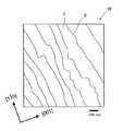
まず、本発明に係るシリコン半導体基板について、図1〜図6を用いて説明する。図1は{110}面を<110>方向に0.1°傾斜した本発明のエピタキシャルシリコン半導体基板WのAFM(Atomic Force Microscope)像を示し、図2はその模式図である。図3は{110}面を<110>方向に7.9°傾斜した本発明のエピタキシャルシリコン半導体基板WのAFM像を示し、図4はその模式図である。図5は{110}面を<110>方向に0.1°傾斜した水素熱処理シリコン半導体基板WのAFM像を示し、図6はその模式図である。
【0038】
本発明のシリコン半導体基板Wは、{110}面又は{110}面を傾けた面を主面とし、その表面に<110>方向に沿った原子レベルのステップSを有するものである(図1〜図6の図示例は{110}面を傾けた面を主面とした場合である)。
【0039】
シリコン半導体基板Wの表面ラフネスを低減するためには、原子レベルでの表面平坦化が必要である。シリコン半導体基板Wの表面にステップSを形成することによって、ステップS間にはテラスTが形成され、そのテラスT面では原子レベルで平坦な面となる。ステップSのエッジを<110>方向になるようにすれば、<110>方向に流れるキャリアは、平坦なテラスT面直下を流れるか、あるいはステップSの段差による散乱を受けることなく流れることによって、表面ラフネスによる散乱の影響が低減され、高い移動度を実現できる。なお、ステップSのエッジは原子レベルでは直線にはならず数原子の凹凸があり、その部分はキンク部と呼ばれる。したがって、<110>方向に沿ったステップSというのは、マイクロメーターオーダーで平均的に見て、<110>方向に沿ったステップSの意味である。
【0040】
{110}面又は{110}面を傾けた面上に形成される半導体集積回路素子のキャリア移動度を高めるには、キャリアが流れる<110>方向の表面が原子レベルで平坦であることが必要である。{110}面又は{110}面を傾けた面を主面とするシリコン半導体基板において、その表面に平均的に<110>方向にステップを形成することができれば、ステップ間に現われる平坦な面であるテラス面の直下を<110>方向に沿ってキャリアを流すことができる。本発明のエピタキシャルシリコン半導体基板は、<110>方向に沿ってステップを形成するために発明されたもので、{110}面を<100>方向に傾けた面を主面とする鏡面研磨シリコン半導体基板表面にエピタキシャル成長によりシリコン単結晶薄膜を形成したものである。
【0041】
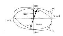
次に、主面が{110}面を<100>方向に傾けた面であるシリコン半導体基板において、オリエンテーションフラットあるいはノッチを<110>方向に形成することについて、図7を用いて説明する。図7は本発明のシリコン半導体基板においてオリエンテーションフラットを<100>方向に付けることによって表裏等価になることを示す説明図である。本発明の効果の一つは、シリコン半導体基板の表裏の管理を不要とすることにある。図7にシリコン半導体基板Wの{110}面を代表して(110)面とし、
【0042】
【外2】
方向にオリエンテーションフラットOF(以下ノッチの場合も同様なのでオリエンテーションフラットで代表する)を形成した場合を示す。(110)面に垂直な[110]軸(矢印OA)を[001]方向に傾けた場合、新たな軸は図中では矢印OA’になる。それにより主面は新たな軸OA’に垂直な面となる。ウェーハの表裏が反転して裏面側を研磨した場合には、傾斜方位はウェーハ下面側に示す矢印OA”となり、傾斜方位はオリエンテーションフラットOFに対して同一方向になる。言い換えれば、オリエンテーションフラットOFを基準にして傾斜方位はウェーハの表裏反転に対して同一方向になる。したがって、シリコン半導体基板の製造工程において、表裏の管理を実施することなく、オリエンテーションフラットOFを基準にして結晶学的に等価な構造をもつシリコン半導体基板を提供できる。
【0044】
比較のために、図8にシリコン半導体基板WのオリエンテーションフラットOFを[001]方向に形成した場合を示す。図7と同様に(110)面に垂直な[110]軸(矢印OA)を[001]方向に傾けた場合、新たな軸は図中では矢印OA’になる。それにより主面は新たな軸OA’に垂直な面となる。ウェーハの表裏が反転して裏面側を研磨した場合には、傾斜方位はウェーハ下面側に示す矢印OA”となり、傾斜方位はオリエンテーションフラットOFに対して180度回転した方向になる。あるウェーハでは傾斜方位はオリエンテーションフラットの方向([001])に向いているが、別のウェーハではオリエンテーションフラットの方向([001])と反対側になる。したがって、オリエンテーションフラットを基準にしてシリコン半導体基板の方向を揃えて種々の処理を施して半導体素子を作製するデバイス作製工程においては、傾斜方向が180度異なるウェーハが混在することになり、同一の特性を示す素子を作製することができなくなる。
【0045】
本発明のシリコン半導体基板の製造方法の第1の態様は、{110}面を<100>方向に傾けた面を主面とするシリコン半導体基板を作製し、その表面にエピタキシャル成長法によりシリコン単結晶薄膜を成長させることにより本発明のシリコン半導体基板を製造するものである。
【0046】
本発明のシリコン半導体基板の製造方法の第2の態様は、{110}面を<100>方向に傾けた面を主面とするシリコン半導体基板を作製し、そのシリコン半導体基板を水素ガス、あるいはアルゴンガス、またはこれらの混合ガス雰囲気中で熱処理することにより本発明のシリコン半導体基板を製造するものである。
【0047】
【実施例】
以下に実施例をあげて本発明をさらに詳細に説明するが、これらの実施例は例示的に示されるもので、限定的に解釈されるべきでないことはいうまでもない。
【0048】
(実施例1)
[110]方向に引き上げられたシリコン単結晶を[001]方向に0°、0.1°、1.0°、2.0°、4.0°、6.0°、7.9°、10.0°傾けて切断し、ウェーハを作製した。結晶はボロンを添加したp型で、電気抵抗率は10〜12Ωcmである。口径は150mmである。切断されたウェーハを通常の化学的機械的研磨によって鏡面ウェーハにした後、RCA洗浄を施した。これらの鏡面研磨シリコン半導体基板にエピタキシャル成長により厚さ約5μmのシリコン単結晶薄膜を形成した。原料ガスとしてトリクロロシラン(SiHCl3)を用い、水素雰囲気中にて1130℃の反応温度で成長させた。
【0049】
表面ラフネスの測定は、AFM(Atomic Force Microscope)の機能によって表面の微小な凹凸を測定することができるSEIKO INSTRUMENTS社のSPA360によって行い、その表面ラフネスの量をRmsによって表す。図9にエピタキシャルシリコン半導体基板のRmsの微傾斜角度依存性を示す。比較のためにそれぞれの傾斜角度をもつ鏡面研磨シリコン半導体基板についても表している。微傾斜角度が0°の場合、鏡面研磨シリコン半導体基板のRmsとエピタキシャルシリコン半導体基板のRmsはそれぞれ0.118nm、0.112nmである。
【0050】
なお、傾斜のない{110}面の鏡面研磨シリコン半導体基板のRms=0.118nmは傾斜のない{100}面の鏡面研磨半導体基板のRmsとほぼ同じ値である。微傾斜角が0.1°においてもエピタキシャルシリコン半導体基板の表面ラフネスは鏡面研磨シリコン半導体基板よりも低減されている。その低減効果は、少なくとも7.9°の傾斜角まで認められる。{110}面の単原子層ステップの段差は0.192nmであるから、7.9°の場合の計算上のテラス幅は1.38nmであり、2原子ステップの段差は0.394nmであるからテラス幅は2.76nmとなり、テラス幅とステップ段差は同じオーダーになる。ステップ間隔が狭くなりその密度が高くなるとキンク密度も高くなり、ステップによる2次元エピタキシャル成長が難しくなる。10.0°では表面ラフネスは悪くなっている。
【0051】
微傾斜角が0.1°のエピタキシャルシリコン半導体基板の表面ラフネスのAFM像を図1に示し、その模式図を図2に示す。図1及び図2に示したように、ステップSとテラスTを認めることができる。ステップSは平均的に<110>方向に形成されている。テラスTの幅は約100nmである。テラスTの幅Lは、簡略化したモデルでステップSの段差hと微傾斜角αの間に成り立つ式:tanα=h/Lによって予測することができる。{110}の場合、単原子ステップの段差は0.192nmで、2原子ステップの段差は0.384nmである。微傾斜角度が0.1°の場合、単原子ステップに対してテラス幅は110nmになる。予測とほぼ一致する。微傾斜角度が1°を超えると、見積もられる単原子ステップによるテラス幅は10nm以下になる。
【0052】
この場合のステップとテラスをAFMで観察することは困難である。表面ラフネスRmsが鏡面研磨シリコン半導体基板よりも低減していることから、ステップとテラスは形成されていると考えられる。このように微傾斜角度が大きくなるほどテラス幅は小さくなると予測されるが、微傾斜角度が7.9°の場合に例外が認められる。その場合のAFM像を図3に示し、その模式図を図4に示す。図3及び図4から明らかなように、予測されるテラス幅である1.38nmまたは2.76nmよりもかなり広いテラスTが形成されている。またステップSの方向は概ね<110>方向であるが、曲線的であることから、ステップSの成長が揺らいでいることを意味している。かなり広いテラスTが形成された理由は、{110}面を<100>方向に7.9°傾けた場合に、その主面は低指数面である{551}面が0.15°傾いた面になることから、その主面がファセット面{551}から僅かに傾いた面になっていることにある。これはファセット面である{111}面を<112>方向に僅かに傾けた場合にステップとテラスが形成されることから推察される。
【0053】
(実施例2)
次に、熱処理シリコン半導体基板の表面ラフネスについて説明する。エピタキシャルシリコン半導体基板の場合と同じように、[110]方向に引き上げられたシリコン単結晶を[001]方向に0°、0.1°、1.0°、2.0°、4.0°、6.0°、7.9°、10.0°傾けて切断し、ウェーハを作製した。通常の化学的機械的研磨によって鏡面ウェーハにした後、RCA洗浄を施した。これらの鏡面研磨シリコン半導体基板に水素ガス雰囲気中で1150℃で1時間の熱処理を施した。図10に水素熱処理シリコン半導体基板のRmsの微傾斜角度依存性を示す。
【0054】
比較のために鏡面研磨シリコン半導体基板についても表している。微傾斜角度が0°の場合、鏡面研磨シリコン半導体基板のRmsと水素熱処理シリコン半導体基板のRmsはそれぞれ0.118nm、0.111nmである。Rmsの微傾斜角度依存性はエピタキシャルシリコン半導体基板の場合と同じである。すなわち微傾斜角が0.1°から7.9°まで水素熱処理シリコン半導体基板の表面ラフネスは鏡面研磨シリコン半導体基板よりも低減されている。
【0055】
図5に微傾斜角が0.1°の場合のAFM像を示し、その模式図を図6に示す。エピタキシャルシリコン半導体基板の場合ほど明瞭ではないがステップとテラスは形成されている。このようにステップとテラスはエピタキシャルシリコン半導体基板に比べて形成され難いといえるが、微傾斜された熱処理シリコン半導体基板の表面ラフネスRmsは鏡面研磨シリコン半導体基板より低減することからキャリアの表面ラフネスによる散乱は低減できる。
【0056】
(実施例3)
以下に、本発明のシリコン半導体基板に半導体素子を形成し、キャリア移動度の測定について説明する。主面が{110}面を<100>方向に傾けた角度を0°、0.1°、7.9°とした鏡面研磨シリコン半導体基板とそれらの表面に厚さ5μmのシリコン単結晶薄膜を成膜されたエピタキシャルシリコン半導体基板及び水素雰囲気中で熱処理を施された熱処理シリコン半導体基板を用いた。鏡面研磨シリコン基板の直径、電気抵抗率、酸素濃度はそれぞれ150mm、p型10〜12Ωcm、16ppma(JEIDA換算)である。エピタキシャルシリコン層の電気抵抗率は11Ωcmを中心値とした。水素熱処理は1150℃で1時間の処理である。参照試料として、傾斜のない{100}面の鏡面研磨シリコン半導体基板も加えた。電気抵抗率、酸素濃度は上記の値とほぼ同じである。なお、JEIDAは日本電子工業振興協会(現在は、JEITA:日本電子情報技術産業協会に改称された)の略称である。
【0057】
電子移動度の改善効果を実証するためにn型電界効果トランジスタを形成した。最初に素子分離のために、STI(Shallow Trench Isolation)法により素子分離のためのトレンチを形成し、シリコン酸化膜(SiO2)によってトレンチを埋めた。次にRCA洗浄を施し、有機物、パーティクル、金属を除去した後、乾燥酸化雰囲気中で5nmのゲート酸化膜を形成した。ゲートの閾値電圧を制御するために基板全面にボロン(B)をイオン注入した。
【0058】
次に、基板全面に多結晶シリコン膜をCVD(Chemical VaporDeposition)法により堆積させ、これをパターニングしてトランジスタ形成領域のゲート酸化膜の上に多結晶シリコン電極を形成した。次に、リン(P)を低濃度でイオン注入して高電界を緩和するn―・ソースとn―・ドレイン領域を形成した。電子の流れる方向は<110>方向である。次にゲート電極を被覆するようにCVDによって基板全面にシリコン酸化膜を堆積させ、異方性エッチングを行ってゲート電極の側壁に側壁絶縁膜を形成した。最後に砒素(As)を高濃度にイオン注入してn+ソースとn+ドレイン領域を形成した。こうして作製されたn型電界効果トランジスタの電子移動度を評価した。
【0059】
基準になる{100}面の鏡面研磨シリコン半導体基板における電子移動度を1として、それぞれの基板の電子移動度を表1に示す。微傾斜エピタキシャルシリコン半導体基板の電子移動度は、現在広く用いられている{100}面鏡面研磨シリコン半導体基板の電子移動度の1.4倍になる。微傾斜された水素熱処理シリコン半導体基板の電子移動度でも約1.2倍になる。微傾斜された鏡面研磨シリコン半導体基板の電子移動度は、{100}面の場合に比べて約0.8倍であり、見劣りするが、傾斜のない{110}面の場合に比べると1.3倍になることから、傾斜することの効果は現われている。この実施例では、半導体素子作製工程で従来のRCA洗浄方法を用いたが、洗浄方法や熱処理方法を改善することによって、電子移動度はさらに改善される可能性がある。例えば、前述の5工程洗浄やラジカル犠牲酸価処理を施すことによって表面ラフネスはさらに改善され、キャリア移動度もさらに高くなるものと期待できる。
【0060】
【表1】
【発明の効果】
以上述べたごとく、本発明のシリコン半導体基板は、原子レベルで平坦化され、従来のシリコン半導体基板に比べて表面ラフネスが約10%低減されること、及び原子レベルの表面ステップが半導体素子のキャリアの流れる方向に沿って形成されることから半導体素子のキャリア移動度を従来のシリコン半導体基板の場合よりも最大で40%も向上させることができる。本発明のシリコン半導体基板を半導体集積回路素子の基板として用いることによって、素子性能の高性能化を実現できる。また、本発明方法によれば、本発明のシリコン半導体基板を効果的に製造することができる。
【図面の簡単な説明】
【図1】実施例1におけるエピタキシャルシリコン半導体基板で傾斜角が0.1°の場合に表面に形成されるステップとテラスの状態を示すAFM像である。
【図2】図1の模式図である。
【図3】実施例1におけるエピタキシャルシリコン半導体基板で微傾斜角が7.9°の場合に表面に形成されるステップとテラスの状態を示すAFM像である。
【図4】図3の模式図である。
【図5】本発明の水素熱処理シリコン半導体基板で微傾斜角が0.1°の場合に表面に形成されるステップとテラスの状態を示すAFM像である。
【図6】図5の模式図である。
【図7】本発明のシリコン半導体基板でオリエンテーションフラットを<110>方向に付けることによって表裏等価になることを示す説明図である。
【図8】シリコン半導体基板でオリエンテーションフラットを<100>方向に付ける場合には表裏等価にならず表裏管理が必要であることを示す説明図である。
【図9】実施例1における本発明のエピタキシャルシリコン半導体基板と鏡面研磨シリコン半導体基板の表面ラフネス(Rms)の微傾斜角度依存性を示すグラフである。
【図10】実施例2における水素熱処理シリコン半導体基板と鏡面研磨シリコン半導体基板の表面ラフネス(Rms)の微傾斜角度依存性を示すグラフである。
【符号の説明】
OF:オリエンテーションフラット、S:ステップ、T:テラス、W:シリコン半導体基板。[0001]
TECHNICAL FIELD OF THE INVENTION
The present invention relates to a single crystal silicon semiconductor substrate used for manufacturing a semiconductor integrated circuit device and a method for manufacturing the same.
[0002]
[Related technology]
A gate insulating film of a MIS • FET (Metal-Insulator-Semiconductor Field Effect Transistor) manufactured using a single crystal silicon wafer has high performance such as low leakage current characteristics, low interface state density, and high resistance to ion implantation. Electrical characteristics and high reliability are required. As a technique for forming a gate insulating film that satisfies these requirements, a technique for forming a silicon dioxide film (sometimes simply referred to as an oxide film) by a thermal oxidation method is mainly used. This is a so-called MOS-FET (Metal-Oxide-Semiconductor Field Effect Transistor). Good thermal oxide film / silicon interface characteristics, oxide film breakdown voltage characteristics, and leak current characteristics can be obtained by this thermal oxidation method when a silicon wafer having {100} as a main surface is used as a substrate. The other main reason why silicon wafers having the principal planes of {110} and {111} orientations are not used as substrates for integrated circuit devices is that oxide films formed on the {110} and {111} planes are not used. This is because the interface state density is high. If the interface state density is high, the electrical characteristics such as the breakdown voltage characteristics and the leak current characteristics of the oxide film are inferior.
[0003]
Therefore, as a silicon wafer substrate on which a MOS-FET is formed, a wafer having a {100} orientation or a wafer inclined about 4 ° from {100} has been used.
[0004]
However, in the case of the {100} plane semiconductor element, it has been a problem that the current driving capability of the p-type FET, that is, the carrier mobility is about 0.3 times that of the n-type FET. In recent years, a technique for forming a high-quality insulating film independent of the plane orientation of the surface of a silicon wafer, that is, a radical oxidation method or a radical nitridation method has been developed (Non-Patent Document 1). By using this method, a high-quality insulating film can be formed on a surface other than {100}.
[0005]
Therefore, the feasibility of a semiconductor integrated circuit device using a silicon semiconductor substrate having a {110} plane as a main surface, which may increase the carrier mobility in the channel direction of the MOSFET, has increased. The present inventors have manufactured a semiconductor device having a {110} plane as a main surface, evaluated its characteristics, and obtained various findings.
[0006]
Although the current driving capability of the p-type FET is increased by about 2.5 times compared to {100}, the result is contrary to the expectation that the current driving capability of the n-type FET is reduced by about 0.6 times. Was. If the electron mobility of this n-type FET can be equal to or higher than the electron mobility of the {100} plane, a semiconductor integrated circuit device using the {110} plane will be practically used and widely used. .
[0007]
Carrier mobility is affected by impurity scattering, phonon scattering (lattice vibration scattering), and surface roughness scattering. When the influence of these scatterings is large, the carrier mobility decreases. It has been clarified that the electron mobility of the {100} plane is greatly affected by the roughness of the silicon surface, and the electron mobility decreases as the roughness becomes worse (Non-Patent Document 2). Thereafter, the following two methods have been proposed as methods for reducing surface roughness. That is, there are methods for cleaning a substrate surface other than (1) forming an oxide film on the surface of a semiconductor substrate in an atmosphere containing oxygen radicals (Non-Patent Document 3) and (2) RCA cleaning (Non-Patent Document 4). .
[0008]
In the radical oxidation of (1), it is highly probable that radical oxygen, which is an oxidizing species, adheres to the protrusions on the silicon surface, and O+And O2+It is considered that the effect of attracting the oxygen ions is synergistic, and the surface roughness is reduced by preferentially oxidizing the protrusion. Conventional oxidation in a dry oxygen (dry oxygen) atmosphere deteriorates the surface roughness by about 20%, while radical oxidation reduces the surface roughness by about 40%.
[0009]
The cleaning method (2) has already been disclosed as Patent Document 1. The cleaning process disclosed in Patent Document 1 is a cleaning process that does not include an alkali solution, and is equal to or more than RCA cleaning, because a cleaning process using an alkaline solution of RCA cleaning that has been widely used conventionally deteriorates surface roughness. It has the ability to remove particles, remove organic contamination, and remove metal impurities. Since this new cleaning step is composed of five steps, it will be abbreviated as a five-step cleaning in this specification.
[0010]
The reason that the surface roughness is deteriorated in the cleaning step including the alkaline solution in the RCA cleaning is that a portion having a weak Si—Si bond is preferentially etched by hydroxide ions (OH ions).
[0011]
Of the above two methods for reducing surface roughness, the radical oxidation method of (1) is a method of reducing surface roughness, but the five-step cleaning of (2) is a method rather than a method of reducing surface roughness. And a method of suppressing the amount of roughness caused by RCA cleaning. Actually, the deterioration of about 50% by the conventional RCA cleaning can be limited to 0% to 10% by the five-step cleaning.
[0012]
Since the surface roughness is reduced by the radical oxidation method, it is possible to further reduce the surface roughness by repeating this radical oxidation before forming the gate oxide film, but there is also a disadvantage of performing the repetition. . The radical oxidation is performed at a low temperature of about 300 ° C. to 500 ° C. At this temperature, an oxygen donor is formed, and the electrical resistivity inside the substrate changes. If the oxidation is performed at 500 ° C. or higher, the formation and growth of oxygen precipitate nuclei also occur on the surface of the substrate, which causes a leak current and a dielectric breakdown of the gate oxide film.
[0013]
Reducing the surface roughness of a silicon semiconductor substrate is to flatten the surface at the atomic level. At the atomic level, the surface of a mirror-polished and cleaned silicon wafer having a specific crystal face has countless irregularities, which is a factor of surface roughness called micro-roughness. This is formed because a large number of micro facets different from the cut surface appear on the surface due to a chemical reaction between a chemical solution used for polishing and cleaning and the silicon surface.
[0014]
In the silicon wafer cut into the {111} plane, the {111} plane itself is a facet plane, so that a flat plane at the atomic level is easily formed. Y. J. Chabal et al. Disclosed that by washing with an aqueous solution of ammonium fluoride, dangling bonds (bonds without a covalent bond partner) of surface silicon atoms can be terminated and stabilized with hydrogen atoms, and atomically flattened. (Non-Patent Document 5).
[0015]
Also, the {111} plane
[0016]
[Outside 1]
It has also been clarified that, by slightly tilting the wafer by several degrees in the direction and washing with an aqueous solution of ammonium fluoride, steps and terraces can be formed at the atomic level and atomically flattened (Non-Patent Document 6). However, among the most widely used {100} plane silicon substrates, there is no report that flattening at the atomic level has been realized only by cleaning a mirror-polished substrate.
[0018]
There is a report that in an epitaxial silicon semiconductor substrate epitaxially grown on a slightly inclined {100} plane, surface roughness was reduced by forming steps and terraces (Non-Patent Document 7). There is also a report that surface roughness is reduced by forming steps and terraces in a silicon semiconductor substrate by performing high-temperature heat treatment in a hydrogen atmosphere (Non-Patent Document 8). However, there is no report on flattening at the atomic level on the {110} plane which the present inventors are paying attention to.
[0019]
Many reports have been made on the flattening of the {100} plane by heat treatment under ultrahigh vacuum. However, it is difficult to introduce a large-diameter silicon substrate having a diameter of 200 mm or more into a silicon substrate manufacturing process because the size of the heat treatment furnace increases and productivity decreases.
[0020]
[Patent Document 1]
JP-A-11-057636
[Non-patent document 1]
2000 Synopsium on VLSI Technology, Honolulu, Hawaii, June 13-15, 2000 "Advanced of Radical Oxidation for Improving Reliability of Ultra-Thin Gathering.
[Non-patent document 2]
T. Ohmi et al. : IEEE Trans. Electron Devices, vol. 137, p. 537, 1992
[Non-Patent Document 3]
M. Nagamine et al. , IEDM Tech. Dig. p. 593, 1998
[Non-patent document 4]
W. See Kern et al. : RCA Review, vol. 31, p. 187, 1970
[Non-Patent Document 5]
Y. J. Chabal et al. , J. et al. Vac. Sci. & Technol. vol. A7, pp. 2104, 1989
[Non-Patent Document 6]
H. Sakaue et al. , Appl. Phys. Lett. vol. 78, p. 309, 2001
[Non-Patent Document 7]
K. Izunom et al. : Jpn. J. Appl. Phys. vol. 31 pp. L1277, 1992
[Non-Patent Document 8]
O. Vatel et al. : Jpn. J. Appl. Phys. vol. 32, pp. L1489, 1993
[0021]
[Problems to be solved by the invention]
From the viewpoint of manufacturing and supplying a silicon semiconductor substrate, improving the surface roughness by the above-described radical oxidation increases the number of steps and lowers productivity. In the current silicon substrate manufacturing process, a process of performing RCA cleaning after mirror polishing is common. Hereinafter, the polished and cleaned silicon semiconductor substrate is referred to as a mirror-polished silicon semiconductor substrate. The term “silicon semiconductor substrate” is used to refer generically to an epitaxial silicon semiconductor substrate and the like. The surface roughness of the mirror-polished silicon semiconductor substrate is about 0.12 nm when expressed in terms of root-mean-square roughness (Rms). Device manufacturers that manufacture semiconductor integrated circuit elements perform RCA cleaning after receiving a silicon semiconductor substrate. As described above, when the RCA cleaning is performed, the surface roughness generally deteriorates.
[0022]
Therefore, a typical Rms of a silicon semiconductor substrate after RCA cleaning in a device maker is about 0.18 nm. When an oxide film of about 5 nm is formed in a conventional dry oxygen (dry oxygen) atmosphere to form a gate oxide film on this substrate, the Rms at the interface is deteriorated to 0.22 nm. On the other hand, when an oxide film of about 5 nm is formed by radical oxidation after the above-described radical sacrificial oxidation, Rms becomes about 0.08 nm, and the surface roughness can be significantly reduced. Introducing this radical sacrificial oxidation process to a silicon semiconductor substrate maker is also one method of reducing surface roughness. However, as described above, the number of processes is increased and productivity is reduced. Therefore, from the standpoint of manufacturing a silicon semiconductor substrate used for manufacturing a semiconductor integrated circuit element, it is possible to manufacture a silicon semiconductor substrate with reduced surface roughness without performing sacrificial oxidation such as radical oxidation or special cleaning. Will be needed.
[0023]
The present invention has been made to manufacture a silicon semiconductor substrate for a semiconductor integrated circuit device in which the carrier mobility of the {110} plane, particularly the mobility of electrons that are carriers of an n-type FET, shows a higher value, A silicon semiconductor substrate whose surface is flattened at an atomic level and surface roughness is reduced by using conventional RCA cleaning without using special cleaning such as the five-step cleaning described above, and without performing radical oxidation, and manufacturing thereof. The aim is to provide a method.
[0024]
[Means for Solving the Problems]
In order to achieve the above object, a first aspect of a silicon semiconductor substrate of the present invention is a silicon semiconductor substrate having a {110} plane or a plane inclined to a {110} plane as a main surface, and the silicon semiconductor substrate has It is characterized by having an atomic level step along the <110> direction on average. It is preferable that the {110} plane is inclined in the <100> direction as the inclined plane of the {110} plane.
[0025]
The greatest feature of using a silicon semiconductor substrate having a {110} plane or a plane inclined to the {110} plane as a main surface for a semiconductor integrated circuit element is that the hole mobility of a p-type FET is <110> in the <110> direction. This is about 2.5 times higher than in the case of the 100 ° plane. Therefore, in a semiconductor integrated circuit device in which the electron mobility of the n-type FET in these silicon semiconductor substrates is improved to the electron mobility of the {100} plane or more, the channel direction in which electrons and holes flow must be formed in the <110> direction. Thereby, further miniaturization of circuit elements can be realized. However, in a silicon semiconductor substrate having a {110} plane as a main surface having no atomic level step in the <110> direction, the surface roughness does not become lower than the surface roughness of the {100} plane, and the electron mobility is {. At present, it is smaller than the electron mobility of the 100 ° plane.
[0026]
In order to reduce the surface roughness, it is necessary to flatten the surface at the atomic level. By forming steps on the surface, terraces are formed between the steps, and the terrace surfaces are flat at the atomic level. If the edge of the step is set to be in the <110> direction, the carrier flowing in the <110> direction flows just below the flat terrace surface or flows without being scattered by the step, thereby causing the carrier to flow due to the surface roughness. The effect of scattering is reduced, and high mobility can be realized. Note that the edge of the step is not a straight line at the atomic level but has irregularities of several atoms, and that portion is called a kink portion. Therefore, a step along the <110> direction means a step along the <110> direction on average in the order of micrometers.
[0027]
In the first aspect of the silicon semiconductor substrate of the present invention, a silicon single crystal thin film can be formed by an epitaxial growth method on a surface of a silicon semiconductor substrate having a {110} plane inclined in the <100> direction as a main surface. . The silicon semiconductor substrate having a silicon single crystal thin film formed on the surface by the epitaxial growth method is, in other words, an epitaxial silicon semiconductor substrate, and may be hereinafter referred to as an epitaxial silicon semiconductor substrate of the present invention.
[0028]
The epitaxial growth of a silicon semiconductor substrate is described by a model in which steps grow two-dimensionally while silicon atoms are deposited on a kink portion of the step formed on the terrace. Terraces and steps are not formed by ordinary RCA cleaning, and countless micro facets are present on the surface of the mirror-polished silicon semiconductor substrate of the {110} plane, whose main surface is not slightly tilted and polished and cleaned. I do. This is the cause of the surface roughness deterioration. When epitaxial growth is performed on this surface, countless microfacets play the role of kinks, and silicon atoms are uniformly deposited. Therefore, steps and terraces oriented in the <110> direction are not formed.
[0029]
However, in the epitaxial silicon semiconductor substrate of the present invention, terraces and steps are not observed despite the fact that the main surface of the mirror-polished silicon semiconductor substrate before epitaxial growth is a finely inclined surface is not observed. When silicon atoms are epitaxially grown on the surface, terraces and steps are formed during the growth process. Since the terrace surface is flat at the atomic level, the surface roughness is improved. The finely polished mirror-polished silicon semiconductor substrate potentially involves the formation of terraces and steps. By setting the direction of the slight inclination to the <100> direction of the present invention, steps appear parallel to the <110> direction, which is the direction in which carriers flow, and the carriers flow just below the terrace surface, which is a flat surface between the steps. Can be. Therefore, carrier scattering due to the step difference does not occur.
[0030]
In the first aspect of the silicon semiconductor substrate of the present invention, a silicon semiconductor substrate having a {110} plane inclined in the <100> direction as a main surface is placed in a hydrogen gas, an argon gas, or a mixed gas atmosphere thereof. (Hereinafter, this silicon semiconductor substrate may be referred to as a heat-treated silicon semiconductor substrate). Even on a vicinal {110} plane silicon substrate that has been heat-treated at high temperature in an atmosphere of hydrogen gas, argon gas, or a mixture of these gases, the silicon atoms on the surface are rearranged by the high-temperature treatment, so that the surface has Steps and terraces are formed. By setting the direction of the slight inclination to be the <100> direction, steps appear parallel to the <110> direction, which is the carrier flowing direction, and the carriers can flow just below the terrace surface which is a flat surface between the steps. Therefore, carrier scattering due to the step difference does not occur.
[0031]
A second aspect of the silicon semiconductor substrate of the present invention is a silicon semiconductor substrate having a principal surface with a {110} plane inclined in the <100> direction, wherein the surface is mirror-polished ( Hereinafter, this silicon semiconductor substrate may be referred to as a mirror-polished silicon semiconductor substrate.) As described above, the steps and terraces are not formed on the silicon substrate that has been slightly polished with the {110} plane in the <100> direction and has been subjected to the polishing and cleaning treatments. Since steps and terraces can be formed by performing heat treatment in an argon gas atmosphere, factors for forming the steps and terraces are inherent in the surface of the silicon substrate. Steps and terraces can be formed in a cleaning step and a heat treatment step in an initial step for forming a semiconductor integrated circuit element.
[0032]
It is preferable that the fine inclination angle in the silicon semiconductor substrate of the present invention is 0 ° or more and less than 8 °. The {110} plane inclined by 8 ° in the <100> direction becomes another low-index plane {551} plane. The {551} plane needs to be slightly inclined to form steps and terraces on this surface. There is. Therefore, less than 8 ° is preferable. As the inclination angle increases, the terrace width decreases and the step density increases. Since the step of the monoatomic layer step on the {110} plane is 0.192 nm, the calculated terrace width in the case of 8 ° is 1.36 nm, and the step width of the two atom step is 0.394 nm, so the terrace width is Is 2.73 nm, and the terrace width and the step height are in the same order. As the density of the steps increases, the kink density also increases, making it difficult to perform two-dimensional epitaxial growth by the steps, so that steps and terraces oriented in a specific direction cannot be formed. The inclusion of 0 ° is due to device accuracy issues. When a wafer is cut from a crystal ingot, even if it is set to 0 °, there is generally an error of about 10 minutes due to accuracy problems between the cutting machine and the direction measuring machine. Therefore, it is extremely rare that a wafer of 0 ° completely becomes 0 °.
[0033]
In the silicon semiconductor substrate of the present invention, it is preferable to form an orientation flat or a notch in the <110> direction. With such a configuration, the inclination direction is the same direction with respect to the front and back of the wafer cut from the crystal ingot, and there is no need to manage the front and back of the wafer, so that the risk of mistaken front and back can be eliminated. it can.
[0034]
A first aspect of the method for manufacturing a silicon semiconductor substrate of the present invention is to manufacture a silicon semiconductor substrate having a {110} plane inclined in the <100> direction as a main surface, and to form a silicon single crystal on the surface by epitaxial growth. The method is characterized in that the silicon semiconductor substrate according to the first aspect of the present invention is manufactured by growing a thin film.
[0035]
In a second aspect of the method for manufacturing a silicon semiconductor substrate according to the present invention, a silicon semiconductor substrate having a principal surface with a {110} plane inclined in the <100> direction is manufactured, and the silicon semiconductor substrate is subjected to hydrogen gas or hydrogen gas. The above-described silicon semiconductor substrate according to the first aspect of the present invention is manufactured by performing heat treatment in an atmosphere of argon gas or a mixed gas thereof.
[0036]
BEST MODE FOR CARRYING OUT THE INVENTION
Hereinafter, embodiments of the present invention will be described with reference to the accompanying drawings. However, it is needless to say that various modifications can be made without departing from the technical idea of the present invention. .
[0037]
First, a silicon semiconductor substrate according to the present invention will be described with reference to FIGS. FIG. 1 shows an AFM (Atomic Force Microscope) image of the epitaxial silicon semiconductor substrate W of the present invention in which the {110} plane is inclined by 0.1 ° in the <110> direction, and FIG. 2 is a schematic diagram thereof. FIG. 3 shows an AFM image of the epitaxial silicon semiconductor substrate W of the present invention in which the {110} plane is inclined by 7.9 ° in the <110> direction, and FIG. 4 is a schematic diagram thereof. FIG. 5 shows an AFM image of the hydrogen heat-treated silicon semiconductor substrate W in which the {110} plane is inclined by 0.1 ° in the <110> direction, and FIG. 6 is a schematic view thereof.
[0038]
The silicon semiconductor substrate W of the present invention has a {110} plane or a plane tilted from the {110} plane as a main surface, and has a step S at an atomic level along the <110> direction on the surface (FIG. 1). 6 shows an example in which a plane inclined from the {110} plane is used as the main plane.
[0039]
In order to reduce the surface roughness of the silicon semiconductor substrate W, it is necessary to planarize the surface at the atomic level. By forming the step S on the surface of the silicon semiconductor substrate W, a terrace T is formed between the steps S, and the terrace T surface becomes a flat surface at an atomic level. If the edge of step S is set to be in the <110> direction, the carriers flowing in the <110> direction flow directly below the flat terrace T surface, or flow without being scattered by the step in step S. The influence of scattering due to surface roughness is reduced, and high mobility can be realized. Note that the edge of step S is not a straight line at the atomic level but has irregularities of several atoms, and that portion is called a kink portion. Therefore, the step S along the <110> direction means the step S along the <110> direction on average in the order of micrometers.
[0040]
In order to increase the carrier mobility of the semiconductor integrated circuit element formed on the {110} plane or the plane inclined from the {110} plane, the surface in the <110> direction in which carriers flow must be flat at the atomic level. It is. In a silicon semiconductor substrate having a {110} plane or a plane inclined to the {110} plane as a main surface, if steps can be formed on the surface in the <110> direction on average, a flat surface appearing between the steps can be formed. The carrier can flow along the <110> direction just below a certain terrace surface. The epitaxial silicon semiconductor substrate of the present invention is invented for forming steps along the <110> direction, and is a mirror-polished silicon semiconductor having a {110} plane inclined in the <100> direction as a main surface. A silicon single crystal thin film is formed on a substrate surface by epitaxial growth.
[0041]
Next, formation of an orientation flat or a notch in the <110> direction in a silicon semiconductor substrate whose main surface is a plane in which the {110} plane is inclined in the <100> direction will be described with reference to FIG. FIG. 7 is an explanatory view showing that the front and back sides are equivalent by attaching an orientation flat in the <100> direction in the silicon semiconductor substrate of the present invention. One of the effects of the present invention is that management of the front and back of a silicon semiconductor substrate is not required. FIG. 7 shows the {110} plane of the silicon semiconductor substrate W as a (110) plane,
[0042]
[Outside 2]
A case is shown in which an orientation flat OF is formed in the direction (hereinafter the same applies to a notch, and is therefore represented by an orientation flat). When the [110] axis (arrow OA) perpendicular to the (110) plane is inclined in the [001] direction, the new axis becomes the arrow OA 'in the figure. Thereby, the main surface becomes a surface perpendicular to the new axis OA '. When the front and back sides of the wafer are reversed and the back side is polished, the tilt direction becomes the arrow OA "shown on the lower surface side of the wafer, and the tilt direction becomes the same direction as the orientation flat OF. In other words, the orientation flat OF Since the tilt direction is the same as the direction of the reversal of the front and back of the wafer in the manufacturing process of the silicon semiconductor substrate, the front and back of the wafer are not crystallized and the crystallographically equivalent orientation is based on the orientation flat OF without performing the management of the front and back. A silicon semiconductor substrate having a structure can be provided.
[0044]
For comparison, FIG. 8 shows a case where the orientation flat OF of the silicon semiconductor substrate W is formed in the [001] direction. When the [110] axis (arrow OA) perpendicular to the (110) plane is inclined in the [001] direction as in FIG. 7, the new axis becomes the arrow OA 'in the figure. Thereby, the main surface becomes a surface perpendicular to the new axis OA '. When the front and back sides of the wafer are inverted and the back side is polished, the tilt direction becomes an arrow OA "shown on the lower surface side of the wafer, and the tilt direction becomes a direction rotated by 180 degrees with respect to the orientation flat OF. The orientation is oriented in the direction of the orientation flat ([001]), but is opposite to the orientation of the orientation flat ([001]) in another wafer. In a device manufacturing process in which semiconductor devices are manufactured by performing various processes in parallel, wafers having different inclination directions by 180 degrees are mixed, and devices having the same characteristics cannot be manufactured.
[0045]
A first aspect of the method for manufacturing a silicon semiconductor substrate of the present invention is to manufacture a silicon semiconductor substrate having a {110} plane inclined in the <100> direction as a main surface, and to form a silicon single crystal on the surface by epitaxial growth. A silicon semiconductor substrate of the present invention is manufactured by growing a thin film.
[0046]
In a second aspect of the method for manufacturing a silicon semiconductor substrate according to the present invention, a silicon semiconductor substrate having a principal surface with a {110} plane inclined in the <100> direction is manufactured, and the silicon semiconductor substrate is subjected to hydrogen gas or hydrogen gas. The silicon semiconductor substrate of the present invention is manufactured by performing heat treatment in an atmosphere of argon gas or a mixed gas thereof.
[0047]
【Example】
Hereinafter, the present invention will be described in more detail with reference to Examples. However, it is needless to say that these Examples are illustrative and should not be construed as limiting.
[0048]
(Example 1)
The silicon single crystal pulled in the [110] direction is moved in the [001] direction by 0 °, 0.1 °, 1.0 °, 2.0 °, 4.0 °, 6.0 °, 7.9 °, The wafer was cut at an angle of 10.0 ° to produce a wafer. The crystal is a p-type doped with boron and has an electrical resistivity of 10 to 12 Ωcm. The diameter is 150 mm. The cut wafer was turned into a mirror-finished wafer by ordinary chemical mechanical polishing, and then subjected to RCA cleaning. A silicon single crystal thin film having a thickness of about 5 μm was formed on these mirror-polished silicon semiconductor substrates by epitaxial growth. Trichlorosilane (SiHCl)3) Was grown at a reaction temperature of 1130 ° C. in a hydrogen atmosphere.
[0049]
The surface roughness is measured by SPA360 of SEIKO INSTRUMENTS, which can measure minute irregularities on the surface by an AFM (Atomic Force Microscope) function, and the amount of the surface roughness is represented by Rms. FIG. 9 shows the dependence of Rms on the inclination angle of the epitaxial silicon semiconductor substrate. For comparison, mirror-polished silicon semiconductor substrates having respective inclination angles are also shown. When the slight inclination angle is 0 °, Rms of the mirror-polished silicon semiconductor substrate and Rms of the epitaxial silicon semiconductor substrate are 0.118 nm and 0.112 nm, respectively.
[0050]
It should be noted that Rms = 0.118 nm of the {110} plane mirror-polished silicon semiconductor substrate without inclination is almost the same value as Rms of the {100} plane mirror-polished semiconductor substrate without inclination. Even at a slight inclination angle of 0.1 °, the surface roughness of the epitaxial silicon semiconductor substrate is lower than that of the mirror-polished silicon semiconductor substrate. The reduction effect is observed at least up to a tilt angle of 7.9 °. Since the step of the monoatomic layer step on the {110} plane is 0.192 nm, the calculated terrace width at 7.9 ° is 1.38 nm, and the step of the two atom step is 0.394 nm. The terrace width is 2.76 nm, and the terrace width and the step height are in the same order. As the step interval becomes narrower and the density increases, the kink density also increases, making it difficult to perform two-dimensional epitaxial growth by the steps. At 10.0 °, the surface roughness is poor.
[0051]
FIG. 1 shows an AFM image of the surface roughness of an epitaxial silicon semiconductor substrate having a fine inclination angle of 0.1 °, and FIG. 2 shows a schematic diagram thereof. As shown in FIGS. 1 and 2, step S and terrace T can be recognized. Step S is formed in the <110> direction on average. The width of the terrace T is about 100 nm. The width L of the terrace T can be predicted by a simplified model: tan α = h / L, which is established between the step h of the step S and the slight inclination angle α. In the case of {110}, the step in a single atom step is 0.192 nm, and the step in a two atom step is 0.384 nm. When the slight inclination angle is 0.1 °, the terrace width is 110 nm for a single atom step. It almost matches the prediction. When the slight inclination angle exceeds 1 °, the estimated terrace width by a single atom step becomes 10 nm or less.
[0052]
In this case, it is difficult to observe the steps and the terrace by the AFM. Since the surface roughness Rms is smaller than that of the mirror-polished silicon semiconductor substrate, it is considered that steps and terraces are formed. As described above, it is predicted that the terrace width becomes smaller as the inclination angle increases, but an exception is recognized when the inclination angle is 7.9 °. An AFM image in that case is shown in FIG. 3, and a schematic diagram thereof is shown in FIG. As is apparent from FIGS. 3 and 4, the terrace T is formed which is considerably wider than the expected terrace width of 1.38 nm or 2.76 nm. The direction of step S is generally the <110> direction, but is curved, which means that the growth of step S is fluctuating. The reason why the rather wide terrace T was formed is that when the {110} plane is tilted by 7.9 ° in the <100> direction, the main surface thereof is tilted by 0.15 ° from the {551} plane which is a low index plane. Therefore, the main surface is slightly inclined from the facet surface {551}. This is inferred from the fact that the steps and terraces are formed when the {111} plane, which is a facet plane, is slightly inclined in the <112> direction.
[0053]
(Example 2)
Next, the surface roughness of the heat-treated silicon semiconductor substrate will be described. As in the case of the epitaxial silicon semiconductor substrate, the silicon single crystal pulled in the [110] direction is moved in the [001] direction by 0 °, 0.1 °, 1.0 °, 2.0 °, and 4.0 °. , 6.0 °, 7.9 °, 10.0 ° and cut to produce a wafer. After turning into a mirror-finished wafer by ordinary chemical mechanical polishing, RCA cleaning was performed. These mirror-polished silicon semiconductor substrates were subjected to a heat treatment at 1150 ° C. for 1 hour in a hydrogen gas atmosphere. FIG. 10 shows the dependence of Rms of the hydrogen heat-treated silicon semiconductor substrate on the slight inclination angle.
[0054]
For comparison, a mirror-polished silicon semiconductor substrate is also shown. When the slight inclination angle is 0 °, Rms of the mirror-polished silicon semiconductor substrate and Rms of the hydrogen heat-treated silicon semiconductor substrate are 0.118 nm and 0.111 nm, respectively. The dependence of Rms on the slight tilt angle is the same as that of the epitaxial silicon semiconductor substrate. That is, the surface roughness of the hydrogen-heat-treated silicon semiconductor substrate is reduced from 0.1 ° to 7.9 ° at a slight inclination angle as compared with the mirror-polished silicon semiconductor substrate.
[0055]
FIG. 5 shows an AFM image when the fine tilt angle is 0.1 °, and FIG. 6 shows a schematic diagram thereof. Although not as clear as in the case of an epitaxial silicon semiconductor substrate, steps and terraces are formed. Thus, it can be said that the steps and terraces are harder to form than the epitaxial silicon semiconductor substrate. However, since the surface roughness Rms of the slightly inclined heat-treated silicon semiconductor substrate is smaller than that of the mirror-polished silicon semiconductor substrate, the scattering due to the surface roughness of the carrier. Can be reduced.
[0056]
(Example 3)
Hereinafter, measurement of carrier mobility by forming a semiconductor element on the silicon semiconductor substrate of the present invention will be described. A mirror-polished silicon semiconductor substrate whose main surface is inclined at an angle of 0 °, 0.1 °, or 7.9 ° with the {110} plane inclined in the <100> direction, and a silicon single crystal thin film having a thickness of 5 μm on the surface thereof An epitaxial silicon semiconductor substrate on which a film was formed and a heat-treated silicon semiconductor substrate heat-treated in a hydrogen atmosphere were used. The diameter, electrical resistivity, and oxygen concentration of the mirror-polished silicon substrate are 150 mm, p-
[0057]
An n-type field effect transistor was formed to demonstrate the effect of improving electron mobility. First, for element isolation, a trench for element isolation is formed by STI (Shallow Trench Isolation), and a silicon oxide film (SiO 2) is formed.2) Filled the trench. Next, RCA cleaning was performed to remove organic substances, particles, and metals, and then a 5 nm gate oxide film was formed in a dry oxidation atmosphere. In order to control the threshold voltage of the gate, boron (B) was ion-implanted over the entire surface of the substrate.
[0058]
Next, a polycrystalline silicon film was deposited on the entire surface of the substrate by a CVD (Chemical Vapor Deposition) method, and this was patterned to form a polycrystalline silicon electrode on the gate oxide film in the transistor formation region. Next, phosphorus (P) was ion-implanted at a low concentration to form n- source and n- drain regions for relaxing a high electric field. The direction in which electrons flow is the <110> direction. Next, a silicon oxide film was deposited on the entire surface of the substrate by CVD so as to cover the gate electrode, and anisotropic etching was performed to form a sidewall insulating film on the sidewall of the gate electrode. Finally, arsenic (As) was ion-implanted at a high concentration to form n + source and n + drain regions. The electron mobility of the n-type field effect transistor thus manufactured was evaluated.
[0059]
Table 1 shows the electron mobility of each of the {100} plane mirror-polished silicon semiconductor substrates as the reference, assuming that the electron mobility is 1. The electron mobility of a vicinal epitaxial silicon semiconductor substrate is 1.4 times the electron mobility of a {100} mirror-polished silicon semiconductor substrate that is currently widely used. The electron mobility of the slightly heat-treated hydrogen-treated silicon semiconductor substrate is also about 1.2 times. The electron mobility of the slightly polished mirror-polished silicon semiconductor substrate is about 0.8 times that of the {100} plane, which is inferior to that of the {110} plane without inclination. Since it is tripled, the effect of tilting is apparent. In this example, the conventional RCA cleaning method was used in the semiconductor element manufacturing process, but the electron mobility may be further improved by improving the cleaning method and the heat treatment method. For example, it is expected that the surface roughness is further improved and the carrier mobility is further increased by performing the above-described five-step cleaning and the radical sacrificial acid value treatment.
[0060]
[Table 1]
【The invention's effect】
As described above, the silicon semiconductor substrate of the present invention is flattened at the atomic level, the surface roughness is reduced by about 10% as compared with the conventional silicon semiconductor substrate, and the atomic level surface step is reduced by the carrier of the semiconductor element. , The carrier mobility of the semiconductor element can be improved by up to 40% as compared with the case of the conventional silicon semiconductor substrate. By using the silicon semiconductor substrate of the present invention as a substrate of a semiconductor integrated circuit device, high performance of the device performance can be realized. Further, according to the method of the present invention, the silicon semiconductor substrate of the present invention can be effectively manufactured.
[Brief description of the drawings]
FIG. 1 is an AFM image showing steps and terraces formed on the surface of an epitaxial silicon semiconductor substrate in Example 1 when the inclination angle is 0.1 °.
FIG. 2 is a schematic diagram of FIG.
FIG. 3 is an AFM image showing states of steps and terraces formed on the surface of the epitaxial silicon semiconductor substrate in Example 1 when the inclination angle is 7.9 °.
FIG. 4 is a schematic diagram of FIG. 3;
FIG. 5 is an AFM image showing states of steps and terraces formed on the surface of the hydrogen-heat-treated silicon semiconductor substrate of the present invention when the fine tilt angle is 0.1 °.
FIG. 6 is a schematic diagram of FIG.
FIG. 7 is an explanatory view showing that the front and back sides are equivalent by attaching an orientation flat in the <110> direction in the silicon semiconductor substrate of the present invention.
FIG. 8 is an explanatory view showing that when an orientation flat is provided in a <100> direction on a silicon semiconductor substrate, the front and back are not equivalent but front and back management is required.
FIG. 9 is a graph showing the dependence of the surface roughness (Rms) of the epitaxial silicon semiconductor substrate of the present invention and the mirror-polished silicon semiconductor substrate on the slight inclination angle in Example 1.
FIG. 10 is a graph showing a slight inclination angle dependency of surface roughness (Rms) of a hydrogen heat-treated silicon semiconductor substrate and a mirror-polished silicon semiconductor substrate in Example 2.
[Explanation of symbols]
OF: orientation flat, S: step, T: terrace, W: silicon semiconductor substrate.
Claims (9)
Translated fromJapanesePriority Applications (7)
| Application Number | Priority Date | Filing Date | Title |
|---|---|---|---|
| JP2003030642AJP4190906B2 (en) | 2003-02-07 | 2003-02-07 | Silicon semiconductor substrate and manufacturing method thereof |
| KR1020057012728AKR101030455B1 (en) | 2003-02-07 | 2004-01-29 | Silicon Semiconductor Substrate and Manufacturing Method Thereof |
| PCT/JP2004/000869WO2004070798A1 (en) | 2003-02-07 | 2004-01-29 | Silicon semiconductor substrate and its manufacturing method |
| US10/543,166US7411274B2 (en) | 2003-02-07 | 2004-01-29 | Silicon semiconductor substrate and its manufacturing method |
| CNB2004800035838ACN100380580C (en) | 2003-02-07 | 2004-01-29 | Silicon semiconductor substrate and manufacturing method thereof |
| EP04706361AEP1592045A4 (en) | 2003-02-07 | 2004-01-29 | SILICON SEMICONDUCTOR SUBSTRATE AND METHOD FOR PRODUCING SAME |
| TW093102420ATW200416806A (en) | 2003-02-07 | 2004-02-03 | Silicon semiconductor substrate and its manufacturing method |
Applications Claiming Priority (1)
| Application Number | Priority Date | Filing Date | Title |
|---|---|---|---|
| JP2003030642AJP4190906B2 (en) | 2003-02-07 | 2003-02-07 | Silicon semiconductor substrate and manufacturing method thereof |
Publications (2)
| Publication Number | Publication Date |
|---|---|
| JP2004265918Atrue JP2004265918A (en) | 2004-09-24 |
| JP4190906B2 JP4190906B2 (en) | 2008-12-03 |
Family
ID=32844274
Family Applications (1)
| Application Number | Title | Priority Date | Filing Date |
|---|---|---|---|
| JP2003030642AExpired - Fee RelatedJP4190906B2 (en) | 2003-02-07 | 2003-02-07 | Silicon semiconductor substrate and manufacturing method thereof |
Country Status (7)
| Country | Link |
|---|---|
| US (1) | US7411274B2 (en) |
| EP (1) | EP1592045A4 (en) |
| JP (1) | JP4190906B2 (en) |
| KR (1) | KR101030455B1 (en) |
| CN (1) | CN100380580C (en) |
| TW (1) | TW200416806A (en) |
| WO (1) | WO2004070798A1 (en) |
Cited By (14)
| Publication number | Priority date | Publication date | Assignee | Title |
|---|---|---|---|---|
| JP2007070131A (en)* | 2005-09-05 | 2007-03-22 | Sumco Corp | Method of manufacturing epitaxial wafer, and epitaxial wafer |
| JP2008177530A (en)* | 2006-12-21 | 2008-07-31 | Covalent Materials Corp | Semiconductor substrate and manufacturing method thereof |
| JP2008177529A (en)* | 2006-12-21 | 2008-07-31 | Covalent Materials Corp | Semiconductor substrate and manufacturing method thereof |
| WO2009044917A1 (en) | 2007-10-04 | 2009-04-09 | National University Corporation Tohoku University | Semiconductor substrate and semiconductor device |
| WO2009150896A1 (en)* | 2008-06-10 | 2009-12-17 | 株式会社Sumco | Silicon epitaxial wafer and method for production thereof |
| JP2010018504A (en)* | 2008-07-14 | 2010-01-28 | Japan Atomic Energy Agency | ONE-DIMENSIONAL NANOSTRUCTURE OF Si(110) SURFACE AND PRODUCTION METHOD OF THE SAME |
| US7989073B2 (en) | 2006-09-05 | 2011-08-02 | Sumco Corporation | Epitaxial silicon wafer and fabrication method thereof |
| JP2012043892A (en)* | 2010-08-17 | 2012-03-01 | Shin Etsu Handotai Co Ltd | Manufacturing method of silicon epitaxial wafer, and silicon epitaxial wafer |
| US8329520B2 (en) | 2009-04-02 | 2012-12-11 | Semiconductor Energy Laboratory Co., Ltd. | Method for manufacturing semiconductor device using a laser annealing process |
| DE112011101708T5 (en) | 2010-05-20 | 2013-02-28 | Shin-Etsu Handotai Co., Ltd. | Epitaxial silicon wafer and method of making the same |
| JPWO2011096417A1 (en)* | 2010-02-04 | 2013-06-10 | 国立大学法人東北大学 | Silicon wafer and semiconductor device |
| JP2013254982A (en)* | 2013-08-21 | 2013-12-19 | Tohoku Univ | Semiconductor substrate and semiconductor device |
| US9157681B2 (en) | 2010-02-04 | 2015-10-13 | National University Corporation Tohoku University | Surface treatment method for atomically flattening a silicon wafer and heat treatment apparatus |
| US9190464B2 (en) | 2013-01-14 | 2015-11-17 | Samsung Electronics Co., Ltd. | Nonvolatile memory devices with aligned trench isolation regions |
Families Citing this family (14)
| Publication number | Priority date | Publication date | Assignee | Title |
|---|---|---|---|---|
| JP2004296496A (en)* | 2003-03-25 | 2004-10-21 | Fujitsu Ltd | Method for manufacturing semiconductor device |
| JP3979412B2 (en)* | 2004-09-29 | 2007-09-19 | 株式会社Sumco | Manufacturing method of silicon epitaxial wafer |
| JP2008060355A (en)* | 2006-08-31 | 2008-03-13 | Sumco Corp | Bonded wafer manufacturing method and bonded wafer |
| US20080164572A1 (en)* | 2006-12-21 | 2008-07-10 | Covalent Materials Corporation | Semiconductor substrate and manufacturing method thereof |
| US8623137B1 (en) | 2008-05-07 | 2014-01-07 | Silicon Genesis Corporation | Method and device for slicing a shaped silicon ingot using layer transfer |
| DE102008026784A1 (en) | 2008-06-04 | 2009-12-10 | Siltronic Ag | Epitaxial silicon wafer with <110> crystal orientation and process for its preparation |
| US9064808B2 (en) | 2011-07-25 | 2015-06-23 | Synopsys, Inc. | Integrated circuit devices having features with reduced edge curvature and methods for manufacturing the same |
| US8609550B2 (en)* | 2011-09-08 | 2013-12-17 | Synopsys, Inc. | Methods for manufacturing integrated circuit devices having features with reduced edge curvature |
| KR102279113B1 (en)* | 2017-04-06 | 2021-07-16 | 가부시키가이샤 사무코 | Method of manufacturing epitaxial silicon wafer and epitaxial silicon wafer |
| US11139402B2 (en) | 2018-05-14 | 2021-10-05 | Synopsys, Inc. | Crystal orientation engineering to achieve consistent nanowire shapes |
| KR102662765B1 (en)* | 2018-08-02 | 2024-05-02 | 삼성전자주식회사 | Substrate, integrated circuit device including substrate, and method of manufacturing integrated circuit device |
| US11264458B2 (en) | 2019-05-20 | 2022-03-01 | Synopsys, Inc. | Crystal orientation engineering to achieve consistent nanowire shapes |
| KR102523367B1 (en)* | 2020-02-13 | 2023-04-21 | 세메스 주식회사 | Method for recovering surface of silicon structure and apparatus for treating substrate |
| CN111364097A (en)* | 2020-04-15 | 2020-07-03 | 晶科能源有限公司 | Single crystal silicon seed crystal, silicon ingot, silicon block, silicon wafer for directional solidification ingot, and preparation method and application thereof |
Family Cites Families (18)
| Publication number | Priority date | Publication date | Assignee | Title |
|---|---|---|---|---|
| US3476991A (en)* | 1967-11-08 | 1969-11-04 | Texas Instruments Inc | Inversion layer field effect device with azimuthally dependent carrier mobility |
| JPS5430004B2 (en) | 1971-09-20 | 1979-09-27 | ||
| JPS59217374A (en) | 1983-05-26 | 1984-12-07 | Toyota Central Res & Dev Lab Inc | Semiconductor strain converter |
| JPS6170748A (en) | 1984-09-14 | 1986-04-11 | Hitachi Ltd | semiconductor equipment |
| US4768076A (en)* | 1984-09-14 | 1988-08-30 | Hitachi, Ltd. | Recrystallized CMOS with different crystal planes |
| EP0354449A3 (en)* | 1988-08-08 | 1991-01-02 | Seiko Epson Corporation | Semiconductor single crystal substrate |
| JPH0274074A (en) | 1988-09-09 | 1990-03-14 | Seiko Epson Corp | semiconductor substrate |
| JPH02248046A (en)* | 1989-03-22 | 1990-10-03 | Nec Corp | Formation of sio2 film |
| CA2172233C (en)* | 1995-03-20 | 2001-01-02 | Lei Zhong | Slant-surface silicon wafer having a reconstructed atomic-level stepped surface structure |
| JPH10199813A (en)* | 1997-01-07 | 1998-07-31 | Mitsubishi Electric Corp | Semiconductor device manufacturing method and semiconductor device |
| JP2001523049A (en)* | 1997-11-10 | 2001-11-20 | スターメガ コーポレイション | Quantum ridges and quantum peaks |
| JP2000216378A (en) | 1999-01-21 | 2000-08-04 | Matsushita Electric Ind Co Ltd | MOS heterostructure, semiconductor device having the structure, and method of manufacturing the same |
| JP4521542B2 (en) | 1999-03-30 | 2010-08-11 | ルネサスエレクトロニクス株式会社 | Semiconductor device and semiconductor substrate |
| JP4016371B2 (en)* | 1999-11-10 | 2007-12-05 | 信越半導体株式会社 | Manufacturing method of silicon epitaxial wafer |
| JP3888416B2 (en)* | 2000-03-09 | 2007-03-07 | 信越半導体株式会社 | Method for manufacturing silicon epitaxial wafer and silicon epitaxial wafer |
| JP2002289819A (en)* | 2001-03-23 | 2002-10-04 | Nippon Steel Corp | SIMOX substrate |
| WO2003049189A1 (en)* | 2001-12-04 | 2003-06-12 | Shin-Etsu Handotai Co.,Ltd. | Pasted wafer and method for producing pasted wafer |
| US7494852B2 (en)* | 2005-01-06 | 2009-02-24 | International Business Machines Corporation | Method for creating a Ge-rich semiconductor material for high-performance CMOS circuits |
- 2003
- 2003-02-07JPJP2003030642Apatent/JP4190906B2/ennot_activeExpired - Fee Related
- 2004
- 2004-01-29CNCNB2004800035838Apatent/CN100380580C/ennot_activeExpired - Lifetime
- 2004-01-29WOPCT/JP2004/000869patent/WO2004070798A1/enactiveApplication Filing
- 2004-01-29KRKR1020057012728Apatent/KR101030455B1/ennot_activeExpired - Lifetime
- 2004-01-29USUS10/543,166patent/US7411274B2/ennot_activeExpired - Lifetime
- 2004-01-29EPEP04706361Apatent/EP1592045A4/ennot_activeCeased
- 2004-02-03TWTW093102420Apatent/TW200416806A/ennot_activeIP Right Cessation
Cited By (22)
| Publication number | Priority date | Publication date | Assignee | Title |
|---|---|---|---|---|
| JP2007070131A (en)* | 2005-09-05 | 2007-03-22 | Sumco Corp | Method of manufacturing epitaxial wafer, and epitaxial wafer |
| US7989073B2 (en) | 2006-09-05 | 2011-08-02 | Sumco Corporation | Epitaxial silicon wafer and fabrication method thereof |
| US8152919B2 (en) | 2006-09-05 | 2012-04-10 | Sumco Corporation | Epitaxial silicon wafer and fabrication method thereof |
| JP2008177530A (en)* | 2006-12-21 | 2008-07-31 | Covalent Materials Corp | Semiconductor substrate and manufacturing method thereof |
| JP2008177529A (en)* | 2006-12-21 | 2008-07-31 | Covalent Materials Corp | Semiconductor substrate and manufacturing method thereof |
| WO2009044917A1 (en) | 2007-10-04 | 2009-04-09 | National University Corporation Tohoku University | Semiconductor substrate and semiconductor device |
| KR101536020B1 (en)* | 2007-10-04 | 2015-07-10 | 고쿠리츠 다이가쿠 호진 도호쿠 다이가쿠 | Semiconductor substrate and semiconductor device |
| JP2009094156A (en)* | 2007-10-04 | 2009-04-30 | Tohoku Univ | Semiconductor substrate and semiconductor device |
| US8492879B2 (en) | 2007-10-04 | 2013-07-23 | National University Corporation Tohoku University | Semiconductor substrate and semiconductor device |
| WO2009150896A1 (en)* | 2008-06-10 | 2009-12-17 | 株式会社Sumco | Silicon epitaxial wafer and method for production thereof |
| JP5212472B2 (en)* | 2008-06-10 | 2013-06-19 | 株式会社Sumco | Manufacturing method of silicon epitaxial wafer |
| US8815710B2 (en) | 2008-06-10 | 2014-08-26 | Sumco Corporation | Silicon epitaxial wafer and method for production thereof |
| JP2010018504A (en)* | 2008-07-14 | 2010-01-28 | Japan Atomic Energy Agency | ONE-DIMENSIONAL NANOSTRUCTURE OF Si(110) SURFACE AND PRODUCTION METHOD OF THE SAME |
| US8329520B2 (en) | 2009-04-02 | 2012-12-11 | Semiconductor Energy Laboratory Co., Ltd. | Method for manufacturing semiconductor device using a laser annealing process |
| JPWO2011096417A1 (en)* | 2010-02-04 | 2013-06-10 | 国立大学法人東北大学 | Silicon wafer and semiconductor device |
| US9157681B2 (en) | 2010-02-04 | 2015-10-13 | National University Corporation Tohoku University | Surface treatment method for atomically flattening a silicon wafer and heat treatment apparatus |
| US8729676B2 (en) | 2010-05-20 | 2014-05-20 | Shin-Etsu Handotai Co., Ltd. | Silicon epitaxial wafer and method for manufacturing the same |
| DE112011101708T5 (en) | 2010-05-20 | 2013-02-28 | Shin-Etsu Handotai Co., Ltd. | Epitaxial silicon wafer and method of making the same |
| KR101625135B1 (en) | 2010-05-20 | 2016-05-27 | 신에쯔 한도타이 가부시키가이샤 | Silicon epitaxial wafer and method for producing same |
| JP2012043892A (en)* | 2010-08-17 | 2012-03-01 | Shin Etsu Handotai Co Ltd | Manufacturing method of silicon epitaxial wafer, and silicon epitaxial wafer |
| US9190464B2 (en) | 2013-01-14 | 2015-11-17 | Samsung Electronics Co., Ltd. | Nonvolatile memory devices with aligned trench isolation regions |
| JP2013254982A (en)* | 2013-08-21 | 2013-12-19 | Tohoku Univ | Semiconductor substrate and semiconductor device |
Also Published As
| Publication number | Publication date |
|---|---|
| TW200416806A (en) | 2004-09-01 |
| EP1592045A4 (en) | 2010-09-08 |
| EP1592045A1 (en) | 2005-11-02 |
| US7411274B2 (en) | 2008-08-12 |
| TWI326103B (en) | 2010-06-11 |
| KR101030455B1 (en) | 2011-04-25 |
| US20060131553A1 (en) | 2006-06-22 |
| CN100380580C (en) | 2008-04-09 |
| KR20050098860A (en) | 2005-10-12 |
| CN1748287A (en) | 2006-03-15 |
| JP4190906B2 (en) | 2008-12-03 |
| WO2004070798A1 (en) | 2004-08-19 |
Similar Documents
| Publication | Publication Date | Title |
|---|---|---|
| JP4190906B2 (en) | Silicon semiconductor substrate and manufacturing method thereof | |
| CN113196499B (en) | Vertical silicon carbide power MOSFET and IGBT and manufacturing method thereof | |
| US7029977B2 (en) | Fabrication method of semiconductor wafer | |
| US9984872B2 (en) | Fabrication and structures of crystalline material | |
| US6180497B1 (en) | Method for producing semiconductor base members | |
| US20070015333A1 (en) | Method for manufacturing silicon carbide semiconductor devices | |
| KR101232470B1 (en) | Semiconductor device and method of manufacturing the same | |
| JP3918565B2 (en) | Manufacturing method of semiconductor device | |
| US20110006310A1 (en) | Semiconductor device and semiconductor device manufacturing method | |
| JP4666200B2 (en) | Method for manufacturing SiC semiconductor device | |
| CN103718299A (en) | Method for manufacturing silicon carbide semiconductor device | |
| JP2008205296A (en) | Silicon carbide semiconductor device and manufacturing method thereof | |
| JP2009149481A (en) | Method for manufacturing semiconductor substrate | |
| JP2005039257A (en) | Semiconductor device and method for manufacturing the same | |
| JP2001035838A (en) | Method for manufacturing silicon carbide semiconductor device | |
| JPH09321323A (en) | Silicon carbide semiconductor substrate, method of manufacturing the same, and silicon carbide semiconductor device using the substrate | |
| JP3963154B2 (en) | Method for manufacturing silicon carbide Schottky barrier diode | |
| CN118610165B (en) | Preparation method of epitaxial GaN HEMT high voltage device on SiC JFET wafer | |
| JP5055687B2 (en) | Manufacturing method of semiconductor wafer | |
| JP4613656B2 (en) | Manufacturing method of semiconductor wafer | |
| CN115810544B (en) | Surface treatment method for gallium oxide-based semiconductor substrate and semiconductor device | |
| CN217158196U (en) | Transistor with a metal gate electrode | |
| US20240021724A1 (en) | GaN TRENCH MOSFET AND FABRICATION METHOD | |
| JP5278132B2 (en) | Manufacturing method of semiconductor device | |
| CN108417488B (en) | Composite insulation structure, transistor and manufacturing method of composite insulation structure and transistor |
Legal Events
| Date | Code | Title | Description |
|---|---|---|---|
| A621 | Written request for application examination | Free format text:JAPANESE INTERMEDIATE CODE: A621 Effective date:20041104 | |
| A131 | Notification of reasons for refusal | Free format text:JAPANESE INTERMEDIATE CODE: A131 Effective date:20080611 | |
| A521 | Request for written amendment filed | Free format text:JAPANESE INTERMEDIATE CODE: A523 Effective date:20080730 | |
| TRDD | Decision of grant or rejection written | ||
| A01 | Written decision to grant a patent or to grant a registration (utility model) | Free format text:JAPANESE INTERMEDIATE CODE: A01 Effective date:20080902 | |
| A01 | Written decision to grant a patent or to grant a registration (utility model) | Free format text:JAPANESE INTERMEDIATE CODE: A01 | |
| A61 | First payment of annual fees (during grant procedure) | Free format text:JAPANESE INTERMEDIATE CODE: A61 Effective date:20080917 | |
| FPAY | Renewal fee payment (event date is renewal date of database) | Free format text:PAYMENT UNTIL: 20110926 Year of fee payment:3 | |
| R150 | Certificate of patent or registration of utility model | Ref document number:4190906 Country of ref document:JP Free format text:JAPANESE INTERMEDIATE CODE: R150 Free format text:JAPANESE INTERMEDIATE CODE: R150 | |
| FPAY | Renewal fee payment (event date is renewal date of database) | Free format text:PAYMENT UNTIL: 20120926 Year of fee payment:4 | |
| R250 | Receipt of annual fees | Free format text:JAPANESE INTERMEDIATE CODE: R250 | |
| FPAY | Renewal fee payment (event date is renewal date of database) | Free format text:PAYMENT UNTIL: 20130926 Year of fee payment:5 | |
| R250 | Receipt of annual fees | Free format text:JAPANESE INTERMEDIATE CODE: R250 | |
| R250 | Receipt of annual fees | Free format text:JAPANESE INTERMEDIATE CODE: R250 | |
| R250 | Receipt of annual fees | Free format text:JAPANESE INTERMEDIATE CODE: R250 | |
| R250 | Receipt of annual fees | Free format text:JAPANESE INTERMEDIATE CODE: R250 | |
| S531 | Written request for registration of change of domicile | Free format text:JAPANESE INTERMEDIATE CODE: R313531 | |
| R350 | Written notification of registration of transfer | Free format text:JAPANESE INTERMEDIATE CODE: R350 | |
| R250 | Receipt of annual fees | Free format text:JAPANESE INTERMEDIATE CODE: R250 | |
| R250 | Receipt of annual fees | Free format text:JAPANESE INTERMEDIATE CODE: R250 | |
| R250 | Receipt of annual fees | Free format text:JAPANESE INTERMEDIATE CODE: R250 | |
| R250 | Receipt of annual fees | Free format text:JAPANESE INTERMEDIATE CODE: R250 | |
| R250 | Receipt of annual fees | Free format text:JAPANESE INTERMEDIATE CODE: R250 | |
| S111 | Request for change of ownership or part of ownership | Free format text:JAPANESE INTERMEDIATE CODE: R313115 | |
| R371 | Transfer withdrawn | Free format text:JAPANESE INTERMEDIATE CODE: R371 | |
| S111 | Request for change of ownership or part of ownership | Free format text:JAPANESE INTERMEDIATE CODE: R313115 | |
| R350 | Written notification of registration of transfer | Free format text:JAPANESE INTERMEDIATE CODE: R350 | |
| R250 | Receipt of annual fees | Free format text:JAPANESE INTERMEDIATE CODE: R250 | |
| LAPS | Cancellation because of no payment of annual fees |