JP2004260041A - Ceramics composite material - Google Patents
Ceramics composite materialDownload PDFInfo
- Publication number
- JP2004260041A JP2004260041AJP2003050408AJP2003050408AJP2004260041AJP 2004260041 AJP2004260041 AJP 2004260041AJP 2003050408 AJP2003050408 AJP 2003050408AJP 2003050408 AJP2003050408 AJP 2003050408AJP 2004260041 AJP2004260041 AJP 2004260041A
- Authority
- JP
- Japan
- Prior art keywords
- layer
- magnetic core
- ceramic
- composite material
- ferrite
- Prior art date
- Legal status (The legal status is an assumption and is not a legal conclusion. Google has not performed a legal analysis and makes no representation as to the accuracy of the status listed.)
- Granted
Links
Images


Landscapes
- Laminated Bodies (AREA)
- Magnetic Ceramics (AREA)
- Compositions Of Oxide Ceramics (AREA)
Abstract
Description
Translated fromJapanese【0001】
【発明の属する技術分野】
本発明はセラミックス複合材料に関するものである。さらに詳細には、磁気ギャップを有する磁心に適用可能であり、直流重畳特性を向上させるインダクタンス素子に有用なセラミックス複合材料に関する。
【0002】
【従来の技術】
一般に変成器やチョークコイル等のインダクタンス素子では直流に交流が重畳されるので、直流磁界による磁気飽和によるインダクタンス値の低下を避けるために磁心に空隙(磁気ギャップ)を設けている。
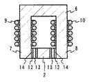
例えば特許文献1のインダクタンス素子では図7に示すように、U字型磁心6の両磁脚7,8に、巻線9,10を巻装し、この磁脚7,8の開放端間にI字状磁心11をギャップ12を形成するように配置した構成とするもので、このように構成することで磁気ギャップ寸法のばらつき要因を少なくし、U字状磁心とI字状磁心の寸法ばらつきだけが磁気ギャップの寸法ばらつきに影響することとなり、インダクタンス値のばらつきを2〜5%程度に低減している。
【0003】
【特許文献1】特開2000−182844
【0004】
【発明が解決しようとする課題】
従来のインダクタンス素子では、U字状磁心6とI字状磁心11とは磁気ギャップ12を形成するように紙材などからなるギャップスペーサ13を介して接着剤14で結合し、または接着剤14だけで結合している。このようなインダクタンス素子ではギャップスペーサ13を配置する手間や、磁気ギャップ12を埋める接着剤14が乾燥硬化するまでに時間がかかり、また硬化までの間、U字状磁心6とI字状磁心11とを保持することが必要であり生産性に劣るものであった。また、多くの接着剤を磁気ギャップに介在させると、膨潤等の経時変化により磁気ギャップ寸法に影響を及ぼしインダクタンス値が変化する問題もあった。
そこで本発明は上述の問題点を解決するためになされたもので、インダクタンス値のばらつきを抑えながら、長期的に電気的特性が安定し、組立が容易で直流重畳特性に優れたインダクタンス素子と、これを構成するセラミックス複合材料からなる磁心を提供することを目的とする。
【0005】
【課題を解決するための手段】
第1の発明は、フェライト層と、アルミナを主成分とするセラミック層と、前記フェライト層と前記セラミック層との間に存在し、FeとAlとが相反する傾斜組成を有する傾斜組成層を備えたセラミックス複合材料である。
前記フェライト層は例えばMn−Zn系、Ni−Zn系、Ni−Cu−Zn系、Mg−Zn系フェライト等であり、Fe、Mn、Zn、Cu、Mg等を主成分とする。またSi,Co,Mn,Mg,Ca等の金属元素を副成分として含有しても良い。また、前記セラミック層を構成するアルミナはα−Al2O3とし前記フェライト層の磁気特性に悪影響を与えないように、純度が少なくとも95wt%以上としておくのが好ましい。不純物として、Fe2O3、SiO2、Na2O、MgO、CaO等を含む場合がある。前記傾斜組成層は前記フェライト層を構成する主成分を含有し、前記フェライト層及び前記セラミック層よりも緻密質として構成される。そして、前記フェライト層の傾斜組成層との界面近傍に空孔を偏在するように構成するの好ましい。
前記傾斜組成層のセラミック層との界面近傍にはAl,Fe等を含む化合物が多く含有すると考えられ、これにより前記セラミック層と前記フェライト層とを傾斜組成層を介して強固に接合させていると推定される。さらにフェライト層の傾斜組成層との界面近傍に空孔を偏在するように構成したので、接合部においてクラックや割れなどのないセラミックス複合材料とすることが出来る。
【0006】
第2の発明は、第1の発明のセラミックス複合材料を用いて構成した磁心である。
【0007】
第3の発明は、第2の発明の磁心を用いて構成したインダクタンス素子である。
【0008】
【発明の実施の形態】
(実施例1)
初めにセラミックス複合材料の作製方法について説明する。
まずフェライト層を構成するMn−Zn系フェライトとして、Fe2O3、ZnO、MnOを焼結後にFe2O3 72wt%、ZnO 5wt%、MnO 23wt%となるように所定量秤量し、これに水及び分散剤を加えて攪拌ミルにて混合し、乾燥後、窒素中にて900℃にて1.5時間仮焼した。仮焼後の原料に水、分散剤を加えて攪拌ミルで混合・粉砕してスラリーとし。これにバインダーを加えてスプレードライヤーで乾燥、造粒した。この造粒粉を金型に充填して仮成形した。そして、所定形状に切り抜いた厚み70μmのAl2O3シートを前記金型内に配置し、さらにその上に造粒粉を充填して、圧力7.3MPaで本成形して、フェライト成形体、Al2O3シート、フェライト成形体が順次積み重なり、焼結後、およそ直径が30mmで厚みが30mmとなる複合成形体とした。
【0009】
ここで、前記Al2O3シートは以下のように準備した。純度が99.6wt%で平均粒子径が0.46μmのα−Al2O3粉末にバインダとしてPVB(ポリビニルブチラール)、可塑剤としてBPBG(ブチルフタリルグリコール酸ブチル)を添加し、エチルアルコールを溶媒としてボールミルにて混合してスラリーとし、脱泡と粘度調整を行い、ドクターブレード法によりグリーンシート(Al2O3シート)を作製した。
【0010】
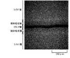
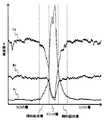
前記複合成形体を、酸素分圧が1〜2%に調整された焼成炉内で、焼成温度1300℃で5時間焼結してフェライト層と、アルミナを主成分とするセラミック層と、前記フェライト層と前記セラミック層との間に存在し傾斜組成層を備えたセラミックス複合材料図1に示すセラミックス複合材料1とした。図2はセラミックス複合材料を厚み方向に切断した断面におけるセラミック層、フェライト層、傾斜組成層を含む領域のSEM−EDX(X線エネルギー分散スペクトルによる走査型電子顕微鏡)による顕微鏡写真である。あわせてEDXでFe,Al、Mnについてライン分析した結果を図3に示す。そして、図2の走査型電子顕微鏡写真で暗色に観察される層(便宜上A層と呼ぶ)と、その両側に形成された組織に空孔が少なく緻密な層(B層と呼ぶ)と、この緻密な層と連続する層(C層と呼ぶ)についてEDX分析により、組成を定量した結果を表1に示す。
【0011】
【表1】
各層の厚みは、A層は40μm〜50μm、B層は60μm〜70μm、残部はC層である。各層の組成を定量した結果、A層は前記Al2O3シートが焼結されて成るアルミナを主成分とするセラミック層であり、C層はMn−Zn系フェライトからなるフェライト層であると特定した。前記セラミック層には、Mn−Zn系フェライトの組成分であるFe2O3とMnOを含有しており、これはMn−Zn系フェライトか拡散したと考えられる。そして、セラミック層とフェライト層との間に介在する空孔が極めて少ない緻密なB層は、セラミック層とフェライト層の組成成分(Fe,Mn、Zn,Al)を含むセラミック層であり、図3のライン分析によれば、FeとAlとが相反する傾斜組成を有するセラミック層、即ち、傾斜組成層であった。この傾斜組成層の厚みは、Al2O3シートを複数枚重ねてセラミック層を厚く形成しても、およそ60μm〜70μm程度の厚みであった。このことから、傾斜組成層はフェライト層とセラミック層の相互拡散層であると推察している。従って、傾斜組成層の厚みは焼成条件(焼成温度、時間等)で制御可能であると考えている。また、前記フェライト層の傾斜組成層との界面近傍を詳細に観察したところ、前記界面近傍でフェライト層側に50μm程度の領域に空孔が偏在していた。
【0013】
断面を詳細に観察したが、接合部においてクラックや割れなどの欠陥は観察されず、本実施例によれば、界面での接合性に優れたセラミックス複合材料を得ることが出来た。
【0014】
(実施例2)
次に、本発明の一実施例に係るセラミックス複合材料を用いて形成したインダクタンス素子20について説明する。図4はこのインダクタンス素子の基本構造を示す外観図である。
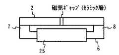
実施例1と同様にして得られたセラミックス複合材料から、長さ30mm、幅5mm、厚み3mmのI字状磁心2を切り出した。また、I字状磁心2のフェライト層を構成するMn−Zn系フェライトを用いてU字状磁心6を形成した。前記U字状磁心の外形寸法を、2つの磁脚7,8を繋ぐ連接部が長さ30mm、幅5mm、厚み3mmで、連接部11からの立設する磁脚の高さが2.5mmとした。前記連接部11にコイルボビンを配置して、前記コイルボビン25に線径φ0.5の線材を10回巻回し、前記磁脚7,8間に橋架けするように、前記I字状磁心2を配置し、I字状磁心2とU字状磁心6の磁脚7,8とが実質的に空隙なく当接するように配置して樹脂粘着テープによりテーピング固定して本実施例に係るインダクタンス素子を構成した。
【0015】
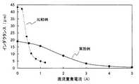
本発明の最も特徴的な所は前記I字状磁心2に形成されたセラミック層で磁気ギャップを構成する点である。この様に磁気ギャップを構成することで、寸法精度に優れ、かつ磁気ギャップの経時変化が実質的に無いインダクタンス素子とすることが出来る。寸法精度良く磁気ギャップを構成できることから、インダクタンス値のばらつきを極めて小さくすることが出来るとともに、従来のインダクタンス素子と比べて、その組み立ても容易となり、結果生産性が向上する。
このインダクタンス素子の直流重畳インダクタンスを室温状態で測定し評価した結果を図5に示す。測定条件はJIS
C2514の直流重畳インダクタンスの測定条件に従い、設定電圧を0.1V、周波数10kHzとした条件で行った。
比較例として、セラミック層を有さない、即ち磁気ギャップを設けないI字状磁心を用いて同様に直流重畳インダクタンスを測定した。本実施例によれば、比較例と比較し優れた直流重畳特性を発揮することがわかる。
【0016】
なお、本実施例では一つの構造体(I字状磁心)にセラミック層を一個所設けた構成であるが、複数個所にセラミック層を形成して一つの構造体に複数の磁気ギャップを構成することが可能である。また、本発明をU字状磁心にも採用することが出来、例えば図6に示すように、U字状磁心6の磁脚6,7の端部にセラミック層を成形することも当然可能である。また、あらためて説明するまでもないが、本発明はI字状磁心、U字状磁心といった形状に限定されず、E字状磁心、棒状磁心、リング状磁心等々、様々な磁心形状に適用可能である。
また、図7(a)(b)に示す磁心の様にセラミック層を一部開口させて形成させても良く、このような磁心を用いたインダクタンス素子では、直流重畳電流が小さい場合には大きなインダクタンス値を有し、直流重畳電流が大きい場合には小さなインダクタンス値となるインダクタンス素子を容易に構成できる。
また、本実施例ではフェライト層をMn−Zn系フェライトとしたが、Ni−Zn系、Ni−Cu−Zn系、Mg−Zn系フェライト等にも適用可能である。
【0017】
【発明の効果】
以上実施例により本発明を詳細に説明したが、本発明によればインダクタンス値のばらつきを抑えながら、長期的に電気的特性が安定し、組立が容易で直流重畳特性に優れたインダクタンス素子と、これを構成するセラミックス複合材料からなる磁心を提供することが出来る。
【図面の簡単な説明】
【図1】本発明の一実施例に係るセラミックス複合材料の斜視図である。
【図2】本発明の一実施例に係るセラミックス複合材料を厚み方向に切断した断面の顕微鏡写真である。
【図3】図2のセラミックス複合材料のEDXによるライン分析結果を示す図である。
【図4】本発明の一実施例に係る磁心を用いたインダクタンス素子の構成を示す外観図である。
【図5】本発明の一実施例に係る磁心を用いたインダクタンス素子と従来のインダクタンス素子の直流重畳特性である。
【図6】本発明の他の実施例に係る磁心を用いたインダクタンス素子の構成を示す外観図である。
【図7】本発明の他の実施例に係る磁心の断面図である。
【図8】従来のインダクタンス素子の構成を示す断面図である。
【符号の説明】
1 セラミックス複合材料
2 I字状磁心
6 U字状磁心
7,8 磁脚
9,10 巻線
12 磁気ギャップ
13 ギャップスペーサ
14 接着剤
20 インダクタンス素子
25 コイルボビン[0001]
TECHNICAL FIELD OF THE INVENTION
The present invention relates to a ceramic composite material. More specifically, the present invention relates to a ceramic composite material that is applicable to a magnetic core having a magnetic gap and is useful for an inductance element that improves DC bias characteristics.
[0002]
[Prior art]
In general, an alternating current is superimposed on a direct current in an inductance element such as a transformer or a choke coil. Therefore, an air gap (magnetic gap) is provided in the magnetic core in order to avoid a decrease in inductance value due to magnetic saturation due to a direct current magnetic field.
For example, in the inductance element of
[0003]
[Patent Document 1] JP-A-2000-182844
[0004]
[Problems to be solved by the invention]
In the conventional inductance element, the U-shaped magnetic core 6 and the I-shaped magnetic core 11 are connected with an adhesive 14 via a
Therefore, the present invention has been made to solve the above problems, while suppressing the variation in inductance value, the electrical characteristics are stable for a long time, the inductance element is easy to assemble and excellent in DC superposition characteristics, and An object of the present invention is to provide a magnetic core made of a ceramic composite material constituting the magnetic core.
[0005]
[Means for Solving the Problems]
The first invention comprises a ferrite layer, a ceramic layer mainly composed of alumina, and a gradient composition layer present between the ferrite layer and the ceramic layer and having a gradient composition in which Fe and Al are contradictory. Ceramic composite material.
The ferrite layer is, for example, a Mn-Zn-based, Ni-Zn-based, Ni-Cu-Zn-based, Mg-Zn-based ferrite or the like, and mainly includes Fe, Mn, Zn, Cu, Mg, and the like. Further, metal elements such as Si, Co, Mn, Mg, and Ca may be contained as auxiliary components. The alumina constituting the ceramic layer is preferably α-Al2 O3, and the purity is preferably at least 95 wt% or more so as not to adversely affect the magnetic properties of the ferrite layer. In some cases, impurities include Fe2 O3 , SiO2 , Na2 O, MgO, CaO, and the like. The gradient composition layer contains a main component constituting the ferrite layer, and is configured to be denser than the ferrite layer and the ceramic layer. It is preferable that the ferrite layer is configured so that holes are unevenly distributed near the interface with the gradient composition layer.
It is considered that a large amount of a compound containing Al, Fe, or the like is contained in the vicinity of the interface between the gradient composition layer and the ceramic layer, whereby the ceramic layer and the ferrite layer are firmly joined via the gradient composition layer. It is estimated to be. Furthermore, since the holes are unevenly distributed in the vicinity of the interface between the ferrite layer and the gradient composition layer, a ceramic composite material free from cracks and cracks at the joint can be obtained.
[0006]
A second invention is a magnetic core formed using the ceramic composite material of the first invention.
[0007]
A third invention is an inductance element configured using the magnetic core of the second invention.
[0008]
BEST MODE FOR CARRYING OUT THE INVENTION
(Example 1)
First, a method for manufacturing a ceramic composite material will be described.
First, as a Mn-Zn-based ferrite constituting a ferrite layer, a predetermined amount of Fe2 O3 , ZnO, and MnO is sintered and weighed so as to be 72 wt% of Fe2 O3 , 5 wt% of ZnO, and 23 wt% of MnO. Water and a dispersant were added, mixed with a stirring mill, dried, and calcined in nitrogen at 900 ° C. for 1.5 hours. Water and a dispersant are added to the calcined raw material and mixed and pulverized with a stirring mill to form a slurry. A binder was added thereto, and the mixture was dried and granulated with a spray drier. This granulated powder was filled in a mold and temporarily molded. Then, an Al2 O3 sheet having a thickness of 70 μm cut out into a predetermined shape is arranged in the mold, and further, granulated powder is filled thereon, and this is molded at a pressure of 7.3 MPa to form a ferrite molded body. An Al2 O3 sheet and a ferrite molded body were sequentially stacked, and after sintering, a composite molded body having a diameter of approximately 30 mm and a thickness of 30 mm was obtained.
[0009]
Here, the Al2 O3 sheet was prepared as follows. PVB (polyvinyl butyral) as a binder and BPBG (butyl butyl phthalyl glycolate) as a plasticizer are added to α-Al2 O3 powder having a purity of 99.6 wt% and an average particle diameter of 0.46 μm, and ethyl alcohol is added. As a solvent, the mixture was mixed with a ball mill to form a slurry, defoaming and viscosity adjustment were performed, and a green sheet (Al2 O3 sheet) was produced by a doctor blade method.
[0010]
Sintering the composite molded body at a firing temperature of 1300 ° C. for 5 hours in a firing furnace in which the oxygen partial pressure is adjusted to 1 to 2%, a ferrite layer, a ceramic layer mainly containing alumina, A ceramic composite material having a gradient composition layer between the ceramic layer and the ceramic layer was prepared as a ceramic
[0011]
[Table 1]
The thickness of each layer is 40 μm to 50 μm for the A layer, 60 μm to 70 μm for the B layer, and the C layer for the rest. As a result of quantifying the composition of each layer, it was specified that the A layer was a ceramic layer mainly composed of alumina obtained by sintering the Al2 O3 sheet, and the C layer was a ferrite layer composed of Mn—Zn ferrite. did. The ceramic layer contains Fe2 O3 and MnO, which are components of Mn—Zn-based ferrite, which is considered to have diffused from the Mn—Zn-based ferrite. The dense B layer having very few voids interposed between the ceramic layer and the ferrite layer is a ceramic layer containing the composition components (Fe, Mn, Zn, Al) of the ceramic layer and the ferrite layer. According to the line analysis, the ceramic layer having a gradient composition in which Fe and Al are opposite to each other, that is, a gradient composition layer. The thickness of the gradient composition layer was approximately 60 μm to 70 μm even when a plurality of Al2 O3 sheets were stacked to form a thick ceramic layer. This suggests that the graded composition layer is an interdiffusion layer between the ferrite layer and the ceramic layer. Therefore, it is considered that the thickness of the gradient composition layer can be controlled by firing conditions (firing temperature, time, etc.). When the vicinity of the interface between the ferrite layer and the gradient composition layer was observed in detail, it was found that vacancies were unevenly distributed in a region of about 50 μm on the ferrite layer side near the interface.
[0013]
Although the cross section was observed in detail, no defects such as cracks and cracks were observed at the joints, and according to this example, a ceramic composite material having excellent joint properties at the interface could be obtained.
[0014]
(Example 2)
Next, an
From the ceramic composite material obtained in the same manner as in Example 1, an I-shaped
[0015]
The most characteristic point of the present invention is that a magnetic gap is formed by the ceramic layer formed on the I-shaped
FIG. 5 shows the results of measuring and evaluating the DC superposed inductance of this inductance element at room temperature. Measurement conditions are JIS
According to the measurement conditions of the DC superimposed inductance of C2514, the measurement was performed under the conditions that the set voltage was 0.1 V and the frequency was 10 kHz.
As a comparative example, a DC superposed inductance was measured in the same manner using an I-shaped magnetic core having no ceramic layer, that is, having no magnetic gap. According to this example, it can be seen that a superior DC superimposition characteristic is exhibited as compared with the comparative example.
[0016]
In this embodiment, one structure (I-shaped magnetic core) is provided with one ceramic layer. However, a plurality of ceramic layers are formed at a plurality of positions to form a plurality of magnetic gaps in one structure. It is possible. Further, the present invention can be applied to a U-shaped magnetic core. For example, as shown in FIG. 6, it is naturally possible to form a ceramic layer on the ends of the magnetic legs 6 and 7 of the U-shaped magnetic core 6. is there. Further, it is needless to say that the present invention is not limited to shapes such as an I-shaped magnetic core and a U-shaped magnetic core, but can be applied to various magnetic core shapes such as an E-shaped magnetic core, a rod-shaped magnetic core, and a ring-shaped magnetic core. is there.
Further, the ceramic layer may be formed by partially opening the ceramic layer like the magnetic core shown in FIGS. 7A and 7B. In the inductance element using such a magnetic core, when the DC superimposed current is small, it is large. An inductance element having an inductance value and having a small inductance value when the DC superimposed current is large can be easily configured.
In this embodiment, the ferrite layer is made of Mn-Zn-based ferrite. However, the present invention can be applied to Ni-Zn-based, Ni-Cu-Zn-based, Mg-Zn-based ferrite, and the like.
[0017]
【The invention's effect】
Although the present invention has been described in detail with the above embodiments, according to the present invention, while suppressing variation in inductance value, electrical characteristics are stable for a long time, an inductance element which is easy to assemble and has excellent DC superimposition characteristics, It is possible to provide a magnetic core made of a ceramic composite material constituting the magnetic core.
[Brief description of the drawings]
FIG. 1 is a perspective view of a ceramic composite material according to one embodiment of the present invention.
FIG. 2 is a photomicrograph of a cross section of the ceramic composite material according to one embodiment of the present invention cut in a thickness direction.
FIG. 3 is a diagram showing a line analysis result of the ceramic composite material of FIG. 2 by EDX.
FIG. 4 is an external view showing a configuration of an inductance element using a magnetic core according to one embodiment of the present invention.
FIG. 5 shows a DC superposition characteristic of an inductance element using a magnetic core according to one embodiment of the present invention and a conventional inductance element.
FIG. 6 is an external view showing a configuration of an inductance element using a magnetic core according to another embodiment of the present invention.
FIG. 7 is a sectional view of a magnetic core according to another embodiment of the present invention.
FIG. 8 is a sectional view showing a configuration of a conventional inductance element.
[Explanation of symbols]
DESCRIPTION OF
Claims (6)
Translated fromJapanesePriority Applications (1)
| Application Number | Priority Date | Filing Date | Title |
|---|---|---|---|
| JP2003050408AJP4362807B2 (en) | 2003-02-27 | 2003-02-27 | Ceramic composite material |
Applications Claiming Priority (1)
| Application Number | Priority Date | Filing Date | Title |
|---|---|---|---|
| JP2003050408AJP4362807B2 (en) | 2003-02-27 | 2003-02-27 | Ceramic composite material |
Publications (2)
| Publication Number | Publication Date |
|---|---|
| JP2004260041Atrue JP2004260041A (en) | 2004-09-16 |
| JP4362807B2 JP4362807B2 (en) | 2009-11-11 |
Family
ID=33115823
Family Applications (1)
| Application Number | Title | Priority Date | Filing Date |
|---|---|---|---|
| JP2003050408AExpired - LifetimeJP4362807B2 (en) | 2003-02-27 | 2003-02-27 | Ceramic composite material |
Country Status (1)
| Country | Link |
|---|---|
| JP (1) | JP4362807B2 (en) |
Cited By (10)
| Publication number | Priority date | Publication date | Assignee | Title |
|---|---|---|---|---|
| JP2006156433A (en)* | 2004-11-25 | 2006-06-15 | Hitachi Metals Ltd | Magnetic core and electronic component using the same |
| JP2006278432A (en)* | 2005-03-28 | 2006-10-12 | Hitachi Metals Ltd | Electronic components |
| JP2006310811A (en)* | 2005-03-28 | 2006-11-09 | Hitachi Metals Ltd | Ferrite component, module and manufacturing methods thereof |
| JP2009266929A (en)* | 2008-04-23 | 2009-11-12 | Daido Steel Co Ltd | Powder magnetic core and its manufacturing method |
| JP2011086810A (en)* | 2009-10-16 | 2011-04-28 | Toyota Industries Corp | Pressed powder core |
| US8153117B2 (en) | 2003-09-08 | 2012-04-10 | Depuy Mitek, Inc. | Chondrocyte therapeutic delivery system |
| US8257963B2 (en) | 2007-06-01 | 2012-09-04 | Depuy Mitek, Inc. | Chondrocyte container and method of use |
| US8354100B2 (en) | 2003-09-08 | 2013-01-15 | Depuy Mitek, Inc. | Chondrocyte therapeutic delivery system |
| JP2015053464A (en)* | 2013-09-09 | 2015-03-19 | 台達電子企業管理(上海)有限公司 | Inductor, and switching circuit including the same |
| JP7613429B2 (en) | 2022-07-29 | 2025-01-15 | 株式会社村田製作所 | Coil parts |
- 2003
- 2003-02-27JPJP2003050408Apatent/JP4362807B2/ennot_activeExpired - Lifetime
Cited By (13)
| Publication number | Priority date | Publication date | Assignee | Title |
|---|---|---|---|---|
| US8354100B2 (en) | 2003-09-08 | 2013-01-15 | Depuy Mitek, Inc. | Chondrocyte therapeutic delivery system |
| US9125888B2 (en) | 2003-09-08 | 2015-09-08 | Depuy Mitek, Llc | Chondrocyte therapeutic delivery system |
| US8153117B2 (en) | 2003-09-08 | 2012-04-10 | Depuy Mitek, Inc. | Chondrocyte therapeutic delivery system |
| US8394369B2 (en) | 2003-09-08 | 2013-03-12 | Depuy Mitek, Inc. | Chondrocyte therapeutic delivery system |
| JP2006156433A (en)* | 2004-11-25 | 2006-06-15 | Hitachi Metals Ltd | Magnetic core and electronic component using the same |
| JP2006278432A (en)* | 2005-03-28 | 2006-10-12 | Hitachi Metals Ltd | Electronic components |
| JP2006310811A (en)* | 2005-03-28 | 2006-11-09 | Hitachi Metals Ltd | Ferrite component, module and manufacturing methods thereof |
| US8592201B2 (en) | 2007-06-01 | 2013-11-26 | Depuy Mitek, Llc | Chondrocyte container and method of use |
| US8257963B2 (en) | 2007-06-01 | 2012-09-04 | Depuy Mitek, Inc. | Chondrocyte container and method of use |
| JP2009266929A (en)* | 2008-04-23 | 2009-11-12 | Daido Steel Co Ltd | Powder magnetic core and its manufacturing method |
| JP2011086810A (en)* | 2009-10-16 | 2011-04-28 | Toyota Industries Corp | Pressed powder core |
| JP2015053464A (en)* | 2013-09-09 | 2015-03-19 | 台達電子企業管理(上海)有限公司 | Inductor, and switching circuit including the same |
| JP7613429B2 (en) | 2022-07-29 | 2025-01-15 | 株式会社村田製作所 | Coil parts |
Also Published As
| Publication number | Publication date |
|---|---|
| JP4362807B2 (en) | 2009-11-11 |
Similar Documents
| Publication | Publication Date | Title |
|---|---|---|
| JP5446262B2 (en) | Laminated parts | |
| US9741484B2 (en) | Laminated coil component | |
| JP5790702B2 (en) | Composite ferrite composition and electronic component | |
| EP1710814B1 (en) | Laminated coil | |
| CN101652336B (en) | Low-loss ferrite and electronic parts using it | |
| KR101475129B1 (en) | Ceramic electronic component and method for producing ceramic electronic component | |
| CN103608876B (en) | Laminated coil component and method of manufacturing the same | |
| KR20100127878A (en) | Multilayer Inductor and Manufacturing Method | |
| JPWO2009087928A1 (en) | Open magnetic circuit type multilayer coil component and manufacturing method thereof | |
| KR20150043038A (en) | Multilayered electronic component | |
| JP2004260041A (en) | Ceramics composite material | |
| JP4596008B2 (en) | Laminated coil | |
| KR101417333B1 (en) | Ferrite ceramic composition, ceramic electronic component, and process for producing ceramic electronic component | |
| WO2010038890A1 (en) | Composite electronic component | |
| JP3975051B2 (en) | Method for manufacturing magnetic ferrite, method for manufacturing multilayer chip ferrite component, and method for manufacturing LC composite multilayer component | |
| JP4524751B2 (en) | Magnetic core and electronic component using the same | |
| DE102008034691A1 (en) | Ceramic multi-layered body comprises ceramic layers with ceramic materials that consist of a determined ceramic sealing tape temperature, and a powder layer with ceramic powder arranged between the ceramic layers | |
| JPH0891919A (en) | Magnetic oxide material composition, its production and inductor, laminated chip inductor and composite laminated part | |
| JP3758464B2 (en) | Laminated electronic components | |
| JP5158829B2 (en) | Electronic components | |
| JP5717056B2 (en) | Ferrite porcelain manufacturing method | |
| JP2005093971A (en) | Multilayer ceramic electronic component | |
| JP2006310811A (en) | Ferrite component, module and manufacturing methods thereof | |
| KR20130006075A (en) | Multilayered coil materials and method for preparing the same | |
| JP2007099539A (en) | Ferrite powder, green sheet containing the ferrite powder, and ferrite sintered compact |
Legal Events
| Date | Code | Title | Description |
|---|---|---|---|
| A621 | Written request for application examination | Free format text:JAPANESE INTERMEDIATE CODE: A621 Effective date:20060113 | |
| A977 | Report on retrieval | Free format text:JAPANESE INTERMEDIATE CODE: A971007 Effective date:20080519 | |
| A131 | Notification of reasons for refusal | Free format text:JAPANESE INTERMEDIATE CODE: A131 Effective date:20080523 | |
| A521 | Request for written amendment filed | Free format text:JAPANESE INTERMEDIATE CODE: A523 Effective date:20080715 | |
| TRDD | Decision of grant or rejection written | ||
| A01 | Written decision to grant a patent or to grant a registration (utility model) | Free format text:JAPANESE INTERMEDIATE CODE: A01 Effective date:20090724 | |
| A01 | Written decision to grant a patent or to grant a registration (utility model) | Free format text:JAPANESE INTERMEDIATE CODE: A01 | |
| A61 | First payment of annual fees (during grant procedure) | Free format text:JAPANESE INTERMEDIATE CODE: A61 Effective date:20090806 | |
| FPAY | Renewal fee payment (event date is renewal date of database) | Free format text:PAYMENT UNTIL: 20120828 Year of fee payment:3 | |
| R150 | Certificate of patent or registration of utility model | Free format text:JAPANESE INTERMEDIATE CODE: R150 Ref document number:4362807 Country of ref document:JP Free format text:JAPANESE INTERMEDIATE CODE: R150 | |
| FPAY | Renewal fee payment (event date is renewal date of database) | Free format text:PAYMENT UNTIL: 20120828 Year of fee payment:3 | |
| FPAY | Renewal fee payment (event date is renewal date of database) | Free format text:PAYMENT UNTIL: 20130828 Year of fee payment:4 | |
| EXPY | Cancellation because of completion of term |