JP2004241504A - Method for manufacturing semiconductor device - Google Patents
Method for manufacturing semiconductor deviceDownload PDFInfo
- Publication number
- JP2004241504A JP2004241504AJP2003027515AJP2003027515AJP2004241504AJP 2004241504 AJP2004241504 AJP 2004241504AJP 2003027515 AJP2003027515 AJP 2003027515AJP 2003027515 AJP2003027515 AJP 2003027515AJP 2004241504 AJP2004241504 AJP 2004241504A
- Authority
- JP
- Japan
- Prior art keywords
- region
- polycrystalline silicon
- channel
- layer
- channel tft
- Prior art date
- Legal status (The legal status is an assumption and is not a legal conclusion. Google has not performed a legal analysis and makes no representation as to the accuracy of the status listed.)
- Pending
Links
Images


Landscapes
- Liquid Crystal (AREA)
- Thin Film Transistor (AREA)
- Recrystallisation Techniques (AREA)
Abstract
Translated fromJapaneseDescription
Translated fromJapanese【0001】
【発明の属する技術分野】
本発明は、アクティブマトリクス型の液晶表示装置及びELパネル表示装置のデータドライバ、ゲートドライバ及び画素スイッチング素子等として用いる多結晶Si薄膜トランジスタへの適用に好適な半導体装置の製造方法に関する。
【0002】
【従来の技術】
従来、薄膜トランジスタ(TFT)がガラス基板等の透明絶縁基板上に形成された液晶表示装置及びELパネル表示装置が製造されている。多くの場合、このような表示装置には、Nチャネル型トランジスタ及びPチャネル型トランジスタが形成されている。
【0003】
図6及び図7は、従来の半導体装置の製造方法を工程順に示す断面図である。従来の製造方法では、先ず、図6(a)に示すように、透明絶縁基板(ガラス基板)101上に、SiO2からなるバッファ層102を400nmの厚さで形成した後、PCVD法によってアモルファスシリコン(a−Si)層103を100nmの厚さで成膜する。このとき、a−Si層103には、成膜時にB2H6ガスを混ぜることにより、低濃度のボロンをドーピングする。
【0004】
次に、窒素雰囲気中で550℃、2時間の熱処理によるa−Si層103の脱水素化を行い、パターニングによって、a−Si層103を所定の帯状の平面形状とする。
【0005】
次いで、図6(b)に示すように、a−Si層103に対して、半導体励起(LD励起)の固体レーザ(DPSSレーザ)であるNd:YVO4により出力6.5W、スキャン速度20cm/秒の条件でレーザ光を照射することにより、a−Si層103を結晶化させ、poly−Si層104とする。その後、poly−Si層104のパターニングを行い、poly−Si層104を所定の島状の平面形状とする。
【0006】
続いて、poly−Si層104上に、SiO2からなるゲート絶縁膜105及びAlからなるゲート電極106を、夫々30nm、300nmの厚さで形成する。
【0007】
次に、図6(b)に示すように、Nチャネル型TFTを形成する領域にのみ開口部が存在するレジストマスク107を形成し、リンのイオン注入を行うことにより、Nチャネル型TFTのソース・ドレイン領域となるn+領域108をpoly−Si層104に形成する。
【0008】
次いで、図6(c)に示すように、レジストマスク107を除去した後、Pチャネル型TFTを形成する領域にのみ開口部が存在するレジストマスク109を形成し、ボロンのイオン注入を行うことにより、Pチャネル型TFTのソース・ドレイン領域となるp+領域110を形成する。
【0009】
その後、図7(a)に示すように、レジストマスク109を除去した後、エキシマレーザアニールにより、不純物の活性化を行う。
【0010】
続いて、図7(b)に示すように、水素注入又は水素プラズマ処理による水素化処理を行う。
【0011】
次に、層間絶縁膜(図示せず)として、厚さが30nmのSiO2膜及び厚さが370nmのSiN膜を順次堆積する。次いで、ソース・ドレイン領域及びゲート電極6に達するコンタクトホールを層間絶縁膜に形成し、Ti膜(100nm)、Al膜(200nm)及びTi膜(100nm)をコンタクトホール内に堆積した後、所定形状のレジストパターンをマスクとしてこれらの金属膜をエッチングすることにより、ソース・ドレイン電極及びゲート引出電極を形成する。
【0012】
ここで、一般的に、多結晶シリコンにおいては、結晶粒界に存在するダングリングボンド等の欠陥がキャリアに対するトラップ準位又は障壁として作用すると考えられている。このため、多結晶シリコン薄膜トランジスタの性能を向上させるためには、前記欠陥を低減させる必要がある。そこで、上述のような従来の半導体装置の製造方法では、水素化処理を行うことにより、水素による前記欠陥の終端化を行っているのである。このような水素化処理の中でも代表的な方法が水素プラズマ処理である。これらの方法を用いると、閾値電圧(スレッシュホルド電圧)Vthの絶対値が小さくなり、サブスレッシュホルド領域の立ち上がりが急峻になる。
【0013】
【特許文献1】
特開2000−196096号公報
【特許文献2】
特開2002−026332号公報
【0014】
【発明が解決しようとする課題】
しかしながら、前述のような水素化処理を行った場合には、オフリーク電流が上昇してしまうという問題点がある。
【0015】
本発明は、かかる問題点に鑑みてなされたものであって、閾値電圧の絶対値を低く抑えながら、オフリーク電流を低下させることができる半導体装置の製造方法を提供することを目的とする。
【0016】
【課題を解決するための手段】
本願発明者は、鋭意検討の結果、オフリーク電流が上昇している理由として、従来の技術では、Nチャネル型トランジスタのId−Vg曲線(ゲート電圧に対するドレイン電流の変化を示す曲線)がデプレッション方向に遷移(シフト)してしまい、その結果、閾値電圧Vthも遷移してしまい、オフリーク電流が上昇していることを見出した。
【0017】
そこで、本願発明者は、このようなNチャネル型トランジスタのId−Vg曲線の遷移を防止すべく、更に鋭意検討を重ねた結果、以下に示す発明の諸態様に想到した。
【0018】
本発明に係る第1の半導体装置の製造方法では、先ず、基板上に、Nチャネル型トランジスタのチャネル、ソース及びドレインとなる第1の多結晶シリコン膜、並びにPチャネル型トランジスタのチャネル、ソース及びドレインとなる第2の多結晶シリコン膜を形成する。次に、前記第1及び第2の多結晶シリコン膜上に、夫々ゲート電極用の導電膜を形成する。そして、前記第1の多結晶シリコン膜又は前記第2の多結晶シリコン膜のいずれか一方のみに水素注入を行う。
【0019】
また、本発明に係る第2の半導体装置の製造方法では、先ず、基板上に、Nチャネル型トランジスタのチャネル、ソース及びドレインとなる第1の多結晶シリコン膜、並びにPチャネル型トランジスタのチャネル、ソース及びドレインとなる第2の多結晶シリコン膜を形成する。次に、前記第1及び第2の多結晶シリコン膜上に、夫々ゲート電極用の導電膜を形成する。そして、前記第1及び第2の多結晶シリコン膜に互いに異なるドーズ量で水素注入を行う。
【0020】
これらの本発明においては、第1の多結晶シリコン膜若しくは第2の多結晶シリコン膜のいずれかのみに水素注入を行うか、又は第1及び第2の多結晶シリコン膜に互いに異なるドーズ量で水素注入を行うため、Pチャネル型トランジスタとNチャネル型トランジスタとの間で、水素注入の程度を互いに独立して制御することが可能である。従って、必要以上のトランジスタ特性(Id−Vg曲線)の遷移を回避することができ、閾値電圧Vthの絶対値が小さく、サブスレッシュホルド領域の立ち上がりが急峻な相補MOSトランジスタ、例えばCMOS多結晶シリコン薄膜トランジスタを得ることができる。更に、Pチャネル型トランジスタ及びNチャネル型トランジスタのいずれにも、エンハンス特性を具備させることも可能である。
【0021】
【発明の実施の形態】
以下、本発明の実施の形態に係る半導体装置の製造方法について添付の図面を参照して具体的に説明する。
【0022】
(第1の実施形態)
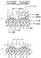
先ず、本発明の第1の実施形態について説明する。図1及び図2は、本発明の第1の実施形態に係る半導体装置の製造方法を工程順に示す断面図である。
【0023】
本実施形態では、先ず、図1(a)に示すように、透明絶縁基板、例えばガラス基板1上に、バッファ層2としてSiO2膜を形成する。バッファ層2の厚さは、例えば400nm程度とする。次に、例えばプラズマCVD法によってアモルファスシリコン(a−Si)層3を成膜する。a−Si層3の厚さは、40nm以上とすることが好ましく、例えば100nm程度とする。このとき、a−Si層3には、成膜時にB2H6ガスを混ぜることにより、P型不純物として、低濃度のボロンをドーピングする。
【0024】
次いで、窒素雰囲気中で550℃、2時間の熱処理によるa−Si層3の脱水素化を行う。その後、a−Si層3のパターニングを行うことにより、その平面形状を、例えば所定の帯状のものとする。
【0025】
続いて、図1(b)に示すように、a−Si層3に対して、例えば半導体励起(LD励起)の固体レーザ(DPSSレーザ)であるNd:YVO4を用い、出力6.5W、スキャン速度20cm/秒の条件でレーザ光を照射することにより、a−Si層3を結晶化させ、poly−Si層4とする。次に、poly−Si層4のパターニングを行うことにより、その平面形状を、例えば所定の島状のものとする。
【0026】
次いで、poly−Si層4上に、ゲート絶縁膜5及びゲート電極6を形成する。ゲート絶縁膜5は、例えばSiO2から形成し、その厚さは、例えば30nm程度とする。また、ゲート電極6は、例えばAlから形成し、その厚さは、例えば300nm程度とする。
【0027】
その後、図1(c)に示すように、Nチャネル型TFTを形成する領域(Nチャネル型TFT形成予定領域)にのみ開口部が存在するレジストマスク7を形成する。そして、レジストマスク7をマスクとして、N型不純物として、例えばリンのイオン注入を行うことにより、Nチャネル型TFTのソース・ドレイン領域となるn+領域8をpoly−Si層4に形成する。なお、Nチャネル型TFT形成予定領域内のpoly−Si層4のうち、ゲート電極6及びゲート絶縁膜5に覆われてリンが注入されない領域は、チャネル領域となる。
【0028】
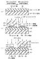
続いて、図2(a)に示すように、レジストマスク7を除去した後、Pチャネル型TFTを形成する領域(Pチャネル型TFT形成予定領域)にのみ開口部が存在するレジストマスク9を形成する。そして、レジストマスク9をマスクとして、P型不純物として、例えばボロンのイオン注入を行うことにより、Pチャネル型TFTのソース・ドレイン領域となるp+領域10を形成する。なお、Pチャネル型TFT形成予定領域内のpoly−Si層4のうち、ゲート電極6及びゲート絶縁膜5に覆われてボロンが注入されない領域は、チャネル領域となる。
【0029】
次に、レジストマスク9を残存させたまま、水素注入を行うことにより、Pチャネル型TFT形成予定領域内において、チャネル領域(poly−Si層4)及びソース・ドレイン領域(p+領域10)の水素化処理を行う。
【0030】
このとき、チャネル領域(poly−Si層4)及びソース・ドレイン領域(p+領域10)の全体にわたって、厚さ方向における水素濃度のプロファイルを実質的に均一なものとすることが好ましい。
【0031】
次いで、図2(b)に示すように、レジストマスク9を除去した後、エキシマレーザを用いたエキシマレーザアニールにより、不純物の活性化を行う。
【0032】
その後、層間絶縁膜(図示せず)として、例えば厚さが30nm程度のSiO2膜及び厚さが370nm程度のSiN膜を順次堆積する。続いて、ソース・ドレイン領域(n+領域8及びp+領域10)及びゲート電極6まで達するコンタクトホールを層間絶縁膜に形成し、Ti膜、Al膜及びTi膜からなる積層膜をコンタクトホール内に堆積する。両Ti膜の厚さ及びAl膜の厚さは、夫々例えば100nm、200nmとする。そして、所定の形状のレジストパターンをマスクとしてこれらの金属膜をエッチングすることにより、ソース・ドレイン電極及びゲート引出電極を形成する。
【0033】
このような第1の実施形態によれば、水素化処理を、レジストマスク9を残存させたまま行っているため、水素化処理はPチャネル型TFTに対してのみ行われる。従って、Nチャネル型TFTにおけるId−Vg曲線の遷移は生じず、閾値電圧Vthの遷移も生じない。
【0034】
(第2の実施形態)
次に、本発明の第2の実施形態について説明する。図3及び図4は、本発明の第2の実施形態に係る半導体装置の製造方法を工程順に示す断面図である。
【0035】
本実施形態では、先ず、図3(a)に示すように、透明絶縁基板、例えばガラス基板1上に、バッファ層2としてSiO2膜を形成する。バッファ層2の厚さは、例えば400nm程度とする。次に、例えばプラズマCVD法によってアモルファスシリコン(a−Si)層3を成膜する。a−Si層3の厚さは、40nm以上とすることが好ましく、例えば100nm程度とする。このとき、a−Si層3には、成膜時にB2H6ガスを混ぜることにより、P型不純物として、低濃度のボロンをドーピングする。
【0036】
次いで、窒素雰囲気中で550℃、2時間の熱処理によるa−Si層3の脱水素化を行う。その後、a−Si層3のパターニングを行うことにより、その平面形状を、例えば所定の帯状のものとする。
【0037】
続いて、図3(b)に示すように、a−Si層3に対して、例えば半導体励起(LD励起)の固体レーザ(DPSSレーザ)であるNd:YVO4を用い、出力6.5W、スキャン速度20cm/秒の条件でレーザ光を照射することにより、a−Si層3を結晶化させ、poly−Si層4とする。次に、poly−Si層4のパターニングを行うことにより、その平面形状を、例えば所定の島状のものとする。
【0038】
次いで、poly−Si層4上に、ゲート絶縁膜5及びゲート電極6を形成する。ゲート絶縁膜5は、例えばSiO2から形成し、その厚さは、例えば30nm程度とする。また、ゲート電極6は、例えばAlから形成し、その厚さは、例えば300nm程度とする。
【0039】
その後、図3(c)に示すように、Nチャネル型TFTを形成する領域(Nチャネル型TFT形成予定領域)にのみ開口部が存在するレジストマスク7を形成する。そして、レジストマスク7をマスクとして、N型不純物として、例えばリンのイオン注入を行うことにより、Nチャネル型TFTのソース・ドレイン領域となるn+領域18をpoly−Si層4に形成する。なお、Nチャネル型TFT形成予定領域内のpoly−Si層4のうち、ゲート電極6及びゲート絶縁膜5に覆われてリンが注入されない領域は、チャネル領域となる。
【0040】
次に、レジストマスク7を残存させたまま、水素注入を行うことにより、Nチャネル型TFT形成予定領域内において、チャネル領域(poly−Si層4)及びソース・ドレイン領域(n+領域18)の水素化処理を行う。この水素化処理では、例えば加速電圧を30keVとし、ドーズ量を5×1014cm−2とする。
【0041】
このとき、チャネル領域(poly−Si層4)及びソース・ドレイン領域(n+領域18)の全体にわたって、厚さ方向における水素濃度のプロファイルを実質的に均一なものとすることが好ましい。
【0042】
続いて、図4(a)に示すように、レジストマスク7を除去した後、Pチャネル型TFTを形成する領域(Pチャネル型TFT形成予定領域)にのみ開口部が存在するレジストマスク9を形成する。そして、レジストマスク9をマスクとして、P型不純物として、例えばボロンのイオン注入を行うことにより、Pチャネル型TFTのソース・ドレイン領域となるp+領域10を形成する。なお、Pチャネル型TFT形成予定領域内のpoly−Si層4のうち、ゲート電極6及びゲート絶縁膜5に覆われてボロンが注入されない領域は、チャネル領域となる。
【0043】
次に、レジストマスク9を残存させたまま、水素注入を行うことにより、Pチャネル型TFTにおいて、チャネル領域(poly−Si層4)及びソース・ドレイン領域(p+領域10)の水素化処理を行う。この水素化処理では、水素のドーズ量を、Nチャネル型TFTに対する水素化処理のときよりも高くし、例えば加速電圧を30keVとし、ドーズ量を1×1015cm−2とする。
【0044】
また、このとき、チャネル領域(poly−Si層4)及びソース・ドレイン領域(p+領域10)の全体にわたって、厚さ方向における水素濃度のプロファイルを実質的に均一なものとすることが好ましい。
【0045】
次いで、図4(b)に示すように、レジストマスク9を除去した後、エキシマレーザを用いたエキシマレーザアニールにより、不純物の活性化を行う。
【0046】
その後、層間絶縁膜(図示せず)として、例えば厚さが30nm程度のSiO2膜及び厚さが370nm程度のSiN膜を順次堆積する。続いて、ソース・ドレイン領域(n+領域8及びp+領域10)及びゲート電極6まで達するコンタクトホールを層間絶縁膜に形成し、Ti膜、Al膜及びTi膜からなる積層膜をコンタクトホール内に堆積する。両Ti膜の厚さ及びAl膜の厚さは、夫々例えば100nm、200nmとする。そして、所定の形状のレジストパターンをマスクとしてこれらの金属膜をエッチングすることにより、ソース・ドレイン電極及びゲート引出電極を形成する。
【0047】
このような第2の実施形態では、水素化処理をNチャネル型TFT形成予定領域に対しても行っているが、Pチャネル型TFT形成予定領域に対する水素化処理とは独立して行っている。このため、互いに独立して水素化処理の程度を制御することができる。従って、必要に応じて、適切な程度で両領域に対して水素化処理を行うことができる。
【0048】
図5は、第2の実施形態によるId−Vg曲線の遷移を示すグラフである。図5中の破線は水素化処理前のId−Vg曲線を示し、実線は水素化処理後のId−Vg曲線を示している。図5に示すように、第2の実施形態では、Nチャネル型TFT及びPチャネル型TFTの双方に水素化処理を施しているため、両TFTにおいて、Id−Vg曲線が遷移している。但し、第2の実施形態では、水素化処理におけるドーズ量を、Pチャネル型TFTでNチャネル型TFTよりも高くしているため、Nチャネル型TFTにおけるId−Vg曲線の遷移が小さく、適切な閾値電圧Vthが得られる。
【0049】
なお、第1の実施形態では、Pチャネル型TFTに対してのみ、第2の実施形態では、Pチャネル型TFT及びNチャネル型TFTの双方に対して、水素化処理を行っているが、水素化処理前のId−Vg曲線によっては、Nチャネル型TFTに対してのみ水素化処理を行うようにしてもよい。
【0050】
以下、本発明の諸態様を付記としてまとめて記載する。
【0051】
(付記1) 基板上に、Nチャネル型トランジスタのチャネル、ソース及びドレインとなる第1の多結晶シリコン膜、並びにPチャネル型トランジスタのチャネル、ソース及びドレインとなる第2の多結晶シリコン膜を形成する工程と、
前記第1及び第2の多結晶シリコン膜上に、夫々ゲート電極用の導電膜を形成する工程と、
前記第1の多結晶シリコン膜又は前記第2の多結晶シリコン膜のいずれか一方のみに水素注入を行う工程と、
を有することを特徴とする半導体装置の製造方法。
【0052】
(付記2) 前記第1の多結晶シリコン膜又は前記第2の多結晶シリコン膜のいずれか一方のみに水素注入を行う工程において、前記第2の多結晶シリコン膜のみに水素注入を行うことを特徴とする付記1に記載の半導体装置の製造方法。
【0053】
(付記3) 基板上に、Nチャネル型トランジスタのチャネル、ソース及びドレインとなる第1の多結晶シリコン膜、並びにPチャネル型トランジスタのチャネル、ソース及びドレインとなる第2の多結晶シリコン膜を形成する工程と、
前記第1及び第2の多結晶シリコン膜上に、夫々ゲート電極用の導電膜を形成する工程と、
前記第1及び第2の多結晶シリコン膜に互いに異なるドーズ量で水素注入を行う工程と、
を有することを特徴とする半導体装置の製造方法。
【0054】
(付記4) 前記第1及び第2の多結晶シリコン膜に互いに異なるドーズ量で水素注入を行う工程において、前記第2の多結晶シリコン膜に、前記第1の多結晶シリコン膜よりも高いドーズ量で水素注入を行うことを特徴とする付記3に記載の半導体装置の製造方法。
【0055】
(付記5) 前記第1及び第2の多結晶シリコン膜を形成する工程において、前記第1及び第2の多結晶シリコン膜にP型不純物を導入することを特徴とする付記1乃至4のいずれか1項に記載の半導体装置の製造方法。
【0056】
(付記6) 前記P型不純物としてボロンを導入することを特徴とする付記5に記載の半導体装置の製造方法。
【0057】
(付記7) 前記第1の多結晶シリコン膜内の厚さ方向における水素濃度のプロファイルを実質的に均一なものとすることを特徴とする付記1乃至6のいずれか1項に記載の半導体装置の製造方法。
【0058】
(付記8) 前記第2の多結晶シリコン膜内の厚さ方向における水素濃度のプロファイルを実質的に均一なものとすることを特徴とする付記1乃至7のいずれか1項に記載の半導体装置の製造方法。
【0059】
(付記9) 前記第1及び第2の多結晶シリコン膜の厚さを40nm以上とすることを特徴とする付記1乃至8のいずれか1項に記載の半導体装置の製造方法。
【0060】
(付記10) 前記水素注入を行う際に、レジストマスクを用いることを特徴とする付記1乃至9のいずれか1項に記載の半導体装置の製造方法。
【0061】
【発明の効果】
以上詳述したように、本発明によれば、一連の工程で用いるマスクの数を増加させることなく、Pチャネル型トランジスタとNチャネル型トランジスタとの間で、水素注入の程度を互いに独立して制御することができる。従って、必要以上の閾値電圧Vthの遷移を抑制することができる。このため、両トランジスタにエンハンスメント特性を具備させることができ、また、オフリーク電流を低下させることができる。このため、本発明を液晶表示装置(LCD)の周辺回路等に適用した場合には、消費電力を低減することが可能である。
【図面の簡単な説明】
【図1】本発明の第1の実施形態に係る半導体装置の製造方法を工程順に示す断面図である。
【図2】図1に引き続き、本発明の第1の実施形態に係る半導体装置の製造方法を工程順に示す断面図である。
【図3】本発明の第2の実施形態に係る半導体装置の製造方法を工程順に示す断面図である。
【図4】図3に引き続き、本発明の第2の実施形態に係る半導体装置の製造方法を工程順に示す断面図である。
【図5】本発明の第2の実施形態によるId−Vg曲線の遷移を示すグラフである。
【図6】従来の半導体装置の製造方法を工程順に示す断面図である。
【図7】図6に引き続き、従来の半導体装置の製造方法を工程順に示す断面図である。
【符号の説明】
1;ガラス基板
2;バッファ層
3;アモルファスシリコン層
4;ポリシリコン層
5;ゲート絶縁膜
6;ゲート電極
7、9;レジストマスク
8、18;n+領域
10;p+領域[0001]
TECHNICAL FIELD OF THE INVENTION
The present invention relates to a method for manufacturing a semiconductor device suitable for application to a polycrystalline Si thin film transistor used as a data driver, a gate driver, a pixel switching element, and the like of an active matrix liquid crystal display device and an EL panel display device.
[0002]
[Prior art]
Conventionally, liquid crystal display devices and EL panel display devices in which thin film transistors (TFTs) are formed on a transparent insulating substrate such as a glass substrate have been manufactured. In many cases, an N-channel transistor and a P-channel transistor are formed in such a display device.
[0003]
6 and 7 are sectional views showing a conventional method for manufacturing a semiconductor device in the order of steps. In the conventional manufacturing method, first, as shown in FIG. 6A, a
[0004]
Next, the a-Si
[0005]
Then, as shown in FIG. 6 (b), with respect to a-Si
[0006]
Subsequently, a
[0007]
Next, as shown in FIG. 6B, a resist mask 107 having an opening only in a region where an N-channel TFT is to be formed is formed, and phosphorus ions are implanted to thereby form a source of the N-channel TFT. -An n+ region 108 serving as a drain region is formed in the poly-
[0008]
Next, as shown in FIG. 6C, after removing the resist mask 107, a
[0009]
After that, as shown in FIG. 7A, the
[0010]
Subsequently, as shown in FIG. 7B, hydrogenation processing by hydrogen injection or hydrogen plasma processing is performed.
[0011]
Next, an SiO2 film having a thickness of 30 nm and a SiN film having a thickness of 370 nm are sequentially deposited as an interlayer insulating film (not shown). Next, a contact hole reaching the source / drain region and the
[0012]
Here, it is generally considered that in polycrystalline silicon, defects such as dangling bonds existing at crystal grain boundaries act as trap levels or barriers for carriers. Therefore, in order to improve the performance of the polycrystalline silicon thin film transistor, it is necessary to reduce the defects. Therefore, in the conventional method for manufacturing a semiconductor device as described above, the hydrogen is terminated to terminate the defect by hydrogen. A typical method among such hydrogenation treatments is a hydrogen plasma treatment. When these methods are used, the absolute value of the threshold voltage (threshold voltage) Vth becomes small, and the rise of the sub-threshold region becomes steep.
[0013]
[Patent Document 1]
JP 2000-196096 A [Patent Document 2]
JP 2002-026332 A
[Problems to be solved by the invention]
However, when the above-described hydrogenation treatment is performed, there is a problem that the off-leak current increases.
[0015]
The present invention has been made in view of such a problem, and an object of the present invention is to provide a method of manufacturing a semiconductor device capable of reducing an off-leak current while keeping an absolute value of a threshold voltage low.
[0016]
[Means for Solving the Problems]
As a result of intensive studies, the present inventor has found that the reason for the increase in off-leakage current is that in the related art, the Id-Vg curve (curve indicating a change in drain current with respect to gate voltage) of an N-channel transistor is in the depletion direction. It has been found that a transition (shift) has occurred, and as a result, the threshold voltage Vth has also transitioned, and the off-leakage current has increased.
[0017]
Then, the inventor of the present application has conducted intensive studies in order to prevent such a transition of the Id-Vg curve of the N-channel transistor, and as a result, came to the following aspects of the invention.
[0018]
In the first method of manufacturing a semiconductor device according to the present invention, first, a first polycrystalline silicon film serving as a channel, a source and a drain of an N-channel transistor, and a channel, a source and a P-channel transistor of a P-channel transistor are formed on a substrate. A second polycrystalline silicon film serving as a drain is formed. Next, a conductive film for a gate electrode is formed on each of the first and second polycrystalline silicon films. Then, hydrogen implantation is performed on only one of the first polycrystalline silicon film and the second polycrystalline silicon film.
[0019]
In the second method for manufacturing a semiconductor device according to the present invention, first, a channel of an N-channel transistor, a first polycrystalline silicon film serving as a source and a drain, and a channel of a P-channel transistor are formed on a substrate. A second polycrystalline silicon film serving as a source and a drain is formed. Next, a conductive film for a gate electrode is formed on each of the first and second polycrystalline silicon films. Then, hydrogen is implanted into the first and second polycrystalline silicon films at different doses.
[0020]
In the present invention, hydrogen is implanted into only either the first polysilicon film or the second polysilicon film, or the first and second polysilicon films are implanted with different doses from each other. Since hydrogen implantation is performed, the degree of hydrogen implantation between the P-channel transistor and the N-channel transistor can be controlled independently of each other. Therefore, it is possible to avoid a transition of the transistor characteristics (Id-Vg curve) more than necessary, a complementary MOS transistor having a small absolute value of the threshold voltage Vth and a steep rise of a sub-threshold region, for example, a CMOS polycrystalline silicon thin film transistor. Can be obtained. Further, both the P-channel transistor and the N-channel transistor can have enhanced characteristics.
[0021]
BEST MODE FOR CARRYING OUT THE INVENTION
Hereinafter, a method for manufacturing a semiconductor device according to an embodiment of the present invention will be specifically described with reference to the accompanying drawings.
[0022]
(1st Embodiment)
First, a first embodiment of the present invention will be described. 1 and 2 are sectional views showing a method of manufacturing a semiconductor device according to the first embodiment of the present invention in the order of steps.
[0023]
In this embodiment, first, as shown in FIG. 1A, an SiO2 film is formed as a buffer layer 2 on a transparent insulating substrate, for example, a
[0024]
Next, dehydrogenation of the
[0025]
Subsequently, as shown in FIG. 1B, an Nd: YVO4 which is a semiconductor-excited (LD-excited) solid-state laser (DPSS laser) is applied to the
[0026]
Next, a
[0027]
Thereafter, as shown in FIG. 1C, a resist mask 7 having an opening only in a region where an N-channel TFT is to be formed (a region where an N-channel TFT is to be formed) is formed. Then, by using the resist mask 7 as a mask and ion-implanting, for example, phosphorus as an N-type impurity, an n+ region 8 serving as a source / drain region of the N-channel TFT is formed in the poly-
[0028]
Subsequently, as shown in FIG. 2A, after removing the resist mask 7, a resist mask 9 having an opening only in a region where a P-channel TFT is to be formed (a region where a P-channel TFT is to be formed) is formed. I do. Then, using the resist mask 9 as a mask, for example, boron is ion-implanted as a P-type impurity to form ap+ region 10 serving as a source / drain region of the P-channel TFT. The region of the poly-
[0029]
Next, by implanting hydrogen with the resist mask 9 remaining, the channel region (poly-Si layer 4) and the source / drain region (p+ region 10) are formed in the region where the P-channel TFT is to be formed. Perform hydrotreating.
[0030]
At this time, it is preferable to make the profile of the hydrogen concentration in the thickness direction substantially uniform over the entire channel region (poly-Si layer 4) and the source / drain region (p+ region 10).
[0031]
Next, as shown in FIG. 2B, after the resist mask 9 is removed, the impurities are activated by excimer laser annealing using an excimer laser.
[0032]
Thereafter, as an interlayer insulating film (not shown), for example, a SiO2 film having a thickness of about 30 nm and a SiN film having a thickness of about 370 nm are sequentially deposited. Subsequently, a contact hole reaching the source / drain region (the n+ region 8 and the p+ region 10) and the
[0033]
According to the first embodiment, since the hydrogenation is performed with the resist mask 9 remaining, the hydrogenation is performed only on the P-channel TFT. Therefore, no transition of the Id-Vg curve occurs in the N-channel TFT, and no transition of the threshold voltage Vth occurs.
[0034]
(Second embodiment)
Next, a second embodiment of the present invention will be described. 3 and 4 are cross-sectional views illustrating a method for manufacturing a semiconductor device according to the second embodiment of the present invention in the order of steps.
[0035]
In this embodiment, first, as shown in FIG. 3A, an SiO2 film is formed as a buffer layer 2 on a transparent insulating substrate, for example, a
[0036]
Next, dehydrogenation of the
[0037]
Subsequently, as shown in FIG. 3B, an Nd: YVO4 which is a semiconductor-excited (LD-excited) solid-state laser (DPSS laser) is applied to the
[0038]
Next, a
[0039]
Thereafter, as shown in FIG. 3C, a resist mask 7 having an opening only in a region where an N-channel TFT is to be formed (a region where an N-channel TFT is to be formed) is formed. Then, using the resist mask 7 as a mask, for example, phosphorus ions are implanted as N-type impurities to form n+ regions 18 serving as source / drain regions of the N-channel TFT in the poly-
[0040]
Next, hydrogen is implanted while the resist mask 7 remains, so that the channel region (poly-Si layer 4) and the source / drain region (n+ region 18) are formed in the N-channel type TFT forming region. Perform hydrotreating. In this hydrogenation treatment, for example, the acceleration voltage is set to 30 keV, and the dose is set to 5 × 1014 cm−2 .
[0041]
At this time, it is preferable to make the profile of the hydrogen concentration in the thickness direction substantially uniform over the entire channel region (poly-Si layer 4) and the source / drain region (n+ region 18).
[0042]
Subsequently, as shown in FIG. 4A, after removing the resist mask 7, a resist mask 9 having an opening only in a region where a P-channel TFT is to be formed (a region where a P-channel TFT is to be formed) is formed. I do. Then, using the resist mask 9 as a mask, for example, boron is ion-implanted as a P-type impurity to form ap+ region 10 serving as a source / drain region of the P-channel TFT. The region of the poly-
[0043]
Next, hydrogen is implanted while the resist mask 9 is left, so that the channel region (poly-Si layer 4) and the source / drain region (p+ region 10) are hydrogenated in the P-channel TFT. Do. In this hydrogenation treatment, the dose of hydrogen is made higher than that in the hydrogenation treatment for the N-channel TFT, for example, the acceleration voltage is set to 30 keV, and the dose is set to 1 × 1015 cm−2 .
[0044]
At this time, it is preferable to make the profile of the hydrogen concentration in the thickness direction substantially uniform throughout the channel region (poly-Si layer 4) and the source / drain region (p+ region 10).
[0045]
Next, as shown in FIG. 4B, after removing the resist mask 9, the impurities are activated by excimer laser annealing using an excimer laser.
[0046]
Thereafter, as an interlayer insulating film (not shown), for example, a SiO2 film having a thickness of about 30 nm and a SiN film having a thickness of about 370 nm are sequentially deposited. Subsequently, a contact hole reaching the source / drain region (the n+ region 8 and the p+ region 10) and the
[0047]
In the second embodiment, the hydrogenation process is also performed on the N-channel TFT forming region, but is performed independently of the P-channel TFT forming region. For this reason, the degree of hydrogenation can be controlled independently of each other. Therefore, if necessary, both regions can be subjected to the hydrogenation treatment to an appropriate degree.
[0048]
FIG. 5 is a graph showing transition of an Id-Vg curve according to the second embodiment. The broken line in FIG. 5 shows the Id-Vg curve before the hydrogenation treatment, and the solid line shows the Id-Vg curve after the hydrogenation treatment. As shown in FIG. 5, in the second embodiment, both the N-channel TFT and the P-channel TFT are subjected to the hydrogenation treatment, so that the Id-Vg curve transitions in both TFTs. However, in the second embodiment, since the dose in the hydrogenation treatment is higher in the P-channel TFT than in the N-channel TFT, the transition of the Id-Vg curve in the N-channel TFT is small, and the The threshold voltage Vth is obtained.
[0049]
In the first embodiment, the hydrogenation is performed only on the P-channel TFT, and in the second embodiment, the hydrogenation is performed on both the P-channel TFT and the N-channel TFT. Depending on the Id-Vg curve before the hydrogenation treatment, the hydrogenation treatment may be performed only on the N-channel TFT.
[0050]
Hereinafter, various aspects of the present invention will be collectively described as supplementary notes.
[0051]
(Supplementary Note 1) A first polycrystalline silicon film serving as a channel, a source, and a drain of an N-channel transistor and a second polycrystalline silicon film serving as a channel, a source, and a drain of a P-channel transistor are formed on a substrate. The process of
Forming a conductive film for a gate electrode on each of the first and second polycrystalline silicon films;
Implanting hydrogen into only one of the first polycrystalline silicon film or the second polycrystalline silicon film;
A method for manufacturing a semiconductor device, comprising:
[0052]
(Supplementary Note 2) In the step of implanting hydrogen into only one of the first polycrystalline silicon film and the second polycrystalline silicon film, it is preferable to implant hydrogen into only the second polycrystalline silicon film. 3. The method for manufacturing a semiconductor device according to
[0053]
(Supplementary Note 3) A first polycrystalline silicon film serving as a channel, a source, and a drain of an N-channel transistor and a second polycrystalline silicon film serving as a channel, a source, and a drain of a P-channel transistor are formed on a substrate. The process of
Forming a conductive film for a gate electrode on each of the first and second polycrystalline silicon films;
Implanting hydrogen into the first and second polycrystalline silicon films at different doses from each other;
A method for manufacturing a semiconductor device, comprising:
[0054]
(Supplementary Note 4) In the step of implanting hydrogen into the first and second polycrystalline silicon films at different doses, the second polycrystalline silicon film may have a higher dose than the first polycrystalline silicon film. The method for manufacturing a semiconductor device according to
[0055]
(Supplementary note 5) Any of the
[0056]
(Supplementary Note 6) The method for manufacturing a semiconductor device according to
[0057]
(Supplementary Note 7) The semiconductor device according to any one of
[0058]
(Supplementary Note 8) The semiconductor device according to any one of
[0059]
(Supplementary Note 9) The method of manufacturing a semiconductor device according to any one of
[0060]
(Supplementary Note 10) The method of manufacturing a semiconductor device according to any one of
[0061]
【The invention's effect】
As described above in detail, according to the present invention, the degree of hydrogen implantation can be independently controlled between a P-channel transistor and an N-channel transistor without increasing the number of masks used in a series of steps. Can be controlled. Therefore, transition of the threshold voltage Vth more than necessary can be suppressed. Therefore, both transistors can be provided with enhancement characteristics, and the off-leak current can be reduced. Therefore, when the present invention is applied to a peripheral circuit of a liquid crystal display (LCD) or the like, power consumption can be reduced.
[Brief description of the drawings]
FIG. 1 is a sectional view illustrating a method for manufacturing a semiconductor device according to a first embodiment of the present invention in the order of steps.
FIG. 2 is a cross-sectional view showing a manufacturing method of the semiconductor device according to the first embodiment of the present invention in the order of steps, following FIG. 1;
FIG. 3 is a sectional view illustrating a method for manufacturing a semiconductor device according to a second embodiment of the present invention in the order of steps.
FIG. 4 is a cross-sectional view showing a manufacturing method of the semiconductor device according to the second embodiment of the present invention in the order of steps, following FIG. 3;
FIG. 5 is a graph showing a transition of an Id-Vg curve according to the second embodiment of the present invention.
FIG. 6 is a sectional view showing a conventional method for manufacturing a semiconductor device in the order of steps.
FIG. 7 is a cross-sectional view showing a conventional method of manufacturing a semiconductor device in the order of steps following FIG. 6;
[Explanation of symbols]
1, glass substrate 2,
Claims (5)
Translated fromJapanese前記第1及び第2の多結晶シリコン膜上に、夫々ゲート電極用の導電膜を形成する工程と、
前記第1の多結晶シリコン膜又は前記第2の多結晶シリコン膜のいずれか一方のみに水素注入を行う工程と、
を有することを特徴とする半導体装置の製造方法。Forming, on a substrate, a first polycrystalline silicon film serving as a channel, a source and a drain of an N-channel transistor, and a second polycrystalline silicon film serving as a channel, a source and a drain of a P-channel transistor;
Forming a conductive film for a gate electrode on each of the first and second polycrystalline silicon films;
Implanting hydrogen into only one of the first polycrystalline silicon film or the second polycrystalline silicon film;
A method for manufacturing a semiconductor device, comprising:
前記第1及び第2の多結晶シリコン膜上に、夫々ゲート電極用の導電膜を形成する工程と、
前記第1及び第2の多結晶シリコン膜に互いに異なるドーズ量で水素注入を行う工程と、
を有することを特徴とする半導体装置の製造方法。Forming, on a substrate, a first polycrystalline silicon film serving as a channel, a source and a drain of an N-channel transistor, and a second polycrystalline silicon film serving as a channel, a source and a drain of a P-channel transistor;
Forming a conductive film for a gate electrode on each of the first and second polycrystalline silicon films;
Implanting hydrogen into the first and second polycrystalline silicon films at different doses from each other;
A method for manufacturing a semiconductor device, comprising:
Priority Applications (1)
| Application Number | Priority Date | Filing Date | Title |
|---|---|---|---|
| JP2003027515AJP2004241504A (en) | 2003-02-04 | 2003-02-04 | Method for manufacturing semiconductor device |
Applications Claiming Priority (1)
| Application Number | Priority Date | Filing Date | Title |
|---|---|---|---|
| JP2003027515AJP2004241504A (en) | 2003-02-04 | 2003-02-04 | Method for manufacturing semiconductor device |
Publications (1)
| Publication Number | Publication Date |
|---|---|
| JP2004241504Atrue JP2004241504A (en) | 2004-08-26 |
Family
ID=32955226
Family Applications (1)
| Application Number | Title | Priority Date | Filing Date |
|---|---|---|---|
| JP2003027515APendingJP2004241504A (en) | 2003-02-04 | 2003-02-04 | Method for manufacturing semiconductor device |
Country Status (1)
| Country | Link |
|---|---|
| JP (1) | JP2004241504A (en) |
Cited By (2)
| Publication number | Priority date | Publication date | Assignee | Title |
|---|---|---|---|---|
| US9685542B2 (en) | 2014-12-30 | 2017-06-20 | Qualcomm Incorporated | Atomic layer deposition of P-type oxide semiconductor thin films |
| US9985139B2 (en) | 2014-11-12 | 2018-05-29 | Qualcomm Incorporated | Hydrogenated p-channel metal oxide semiconductor thin film transistors |
- 2003
- 2003-02-04JPJP2003027515Apatent/JP2004241504A/enactivePending
Cited By (2)
| Publication number | Priority date | Publication date | Assignee | Title |
|---|---|---|---|---|
| US9985139B2 (en) | 2014-11-12 | 2018-05-29 | Qualcomm Incorporated | Hydrogenated p-channel metal oxide semiconductor thin film transistors |
| US9685542B2 (en) | 2014-12-30 | 2017-06-20 | Qualcomm Incorporated | Atomic layer deposition of P-type oxide semiconductor thin films |
Similar Documents
| Publication | Publication Date | Title |
|---|---|---|
| US5834071A (en) | Method for forming a thin film transistor | |
| US20040195568A1 (en) | Thin film transistor substrate and method for manufacturing the same | |
| JP3865145B2 (en) | Method for manufacturing semiconductor device | |
| US7871872B2 (en) | Method of manufacturing thin film transistor having lightly doped drain regions | |
| JP2001028448A (en) | Method for manufacturing thin film transistor | |
| KR19980016968A (en) | Self-aligned thin film transistor manufacturing method | |
| KR100588174B1 (en) | Method of fabricating thin film transistor | |
| KR100776362B1 (en) | Crystallization Method of Amorphous Silicon Thin Film and Manufacturing Method of Polycrystalline Silicon Thin Film Transistor Using the Same | |
| KR100653298B1 (en) | Manufacturing Method of Thin Film Transistor | |
| JP5540723B2 (en) | Thin film transistor manufacturing method | |
| KR100815894B1 (en) | Manufacturing Method of CMOS Polycrystalline Silicon Thin Film Transistor of Ldd Structure | |
| JPH09321305A (en) | Thin film transistor and liquid crystal display device using the same | |
| KR100205069B1 (en) | Fabrication method of polysilicon thin film transistor | |
| JP2004241504A (en) | Method for manufacturing semiconductor device | |
| JP2933121B2 (en) | Method for manufacturing thin film transistor | |
| JP3398665B2 (en) | Method for manufacturing thin film transistor | |
| JP4354099B2 (en) | Thin film transistor manufacturing method | |
| JP3765936B2 (en) | Method for manufacturing semiconductor device | |
| JP3140304B2 (en) | Semiconductor device and manufacturing method thereof | |
| KR100552936B1 (en) | Method for manufacturing crystalline thin film transistor including metal offset region | |
| JP2705550B2 (en) | CMOS thin film transistor and method of manufacturing the same | |
| JP4461731B2 (en) | Thin film transistor manufacturing method | |
| JP3413699B2 (en) | Semiconductor device and manufacturing method thereof | |
| JP3765975B2 (en) | Semiconductor device | |
| JP2000004021A (en) | Active matrix array for thin film transistor and liquid crystal display device and method for manufacturing the same |
Legal Events
| Date | Code | Title | Description |
|---|---|---|---|
| A711 | Notification of change in applicant | Free format text:JAPANESE INTERMEDIATE CODE: A711 Effective date:20050713 | |
| RD02 | Notification of acceptance of power of attorney | Free format text:JAPANESE INTERMEDIATE CODE: A7422 Effective date:20050803 | |
| A621 | Written request for application examination | Free format text:JAPANESE INTERMEDIATE CODE: A621 Effective date:20051202 | |
| A977 | Report on retrieval | Free format text:JAPANESE INTERMEDIATE CODE: A971007 Effective date:20080827 | |
| A131 | Notification of reasons for refusal | Free format text:JAPANESE INTERMEDIATE CODE: A131 Effective date:20080902 | |
| A02 | Decision of refusal | Free format text:JAPANESE INTERMEDIATE CODE: A02 Effective date:20090127 |