JP2004233715A - Active driving type pixel structure and its inspecting method - Google Patents
Active driving type pixel structure and its inspecting methodDownload PDFInfo
- Publication number
- JP2004233715A JP2004233715AJP2003023034AJP2003023034AJP2004233715AJP 2004233715 AJP2004233715 AJP 2004233715AJP 2003023034 AJP2003023034 AJP 2003023034AJP 2003023034 AJP2003023034 AJP 2003023034AJP 2004233715 AJP2004233715 AJP 2004233715A
- Authority
- JP
- Japan
- Prior art keywords
- tft
- dummy load
- current
- control
- inspection
- Prior art date
- Legal status (The legal status is an assumption and is not a legal conclusion. Google has not performed a legal analysis and makes no representation as to the accuracy of the status listed.)
- Granted
Links
- 238000000034methodMethods0.000titleclaimsdescription38
- 238000007689inspectionMethods0.000claimsabstractdescription75
- 239000003990capacitorSubstances0.000claimsabstractdescription47
- 238000012360testing methodMethods0.000claimsdescription31
- 238000012545processingMethods0.000claimsdescription4
- 238000010276constructionMethods0.000claims1
- 239000010409thin filmSubstances0.000abstractdescription2
- 238000010586diagramMethods0.000description13
- 239000011159matrix materialSubstances0.000description12
- 230000007547defectEffects0.000description11
- 230000000694effectsEffects0.000description11
- 239000011265semifinished productSubstances0.000description8
- 239000000758substrateSubstances0.000description5
- 238000012937correctionMethods0.000description4
- 230000002950deficientEffects0.000description4
- 230000008901benefitEffects0.000description2
- 239000010408filmSubstances0.000description2
- 238000005259measurementMethods0.000description2
- 239000000047productSubstances0.000description2
- 230000009471actionEffects0.000description1
- 238000007664blowingMethods0.000description1
- 230000008859changeEffects0.000description1
- 230000007423decreaseEffects0.000description1
- 238000005401electroluminescenceMethods0.000description1
- 239000004973liquid crystal related substanceSubstances0.000description1
- 150000002894organic compoundsChemical class0.000description1
- 239000011368organic materialSubstances0.000description1
- 230000008569processEffects0.000description1
- 230000009467reductionEffects0.000description1
- 239000000523sampleSubstances0.000description1
Images


Classifications
- G—PHYSICS
- G09—EDUCATION; CRYPTOGRAPHY; DISPLAY; ADVERTISING; SEALS
- G09G—ARRANGEMENTS OR CIRCUITS FOR CONTROL OF INDICATING DEVICES USING STATIC MEANS TO PRESENT VARIABLE INFORMATION
- G09G3/00—Control arrangements or circuits, of interest only in connection with visual indicators other than cathode-ray tubes
- G09G3/20—Control arrangements or circuits, of interest only in connection with visual indicators other than cathode-ray tubes for presentation of an assembly of a number of characters, e.g. a page, by composing the assembly by combination of individual elements arranged in a matrix no fixed position being assigned to or needed to be assigned to the individual characters or partial characters
- G09G3/22—Control arrangements or circuits, of interest only in connection with visual indicators other than cathode-ray tubes for presentation of an assembly of a number of characters, e.g. a page, by composing the assembly by combination of individual elements arranged in a matrix no fixed position being assigned to or needed to be assigned to the individual characters or partial characters using controlled light sources
- G09G3/30—Control arrangements or circuits, of interest only in connection with visual indicators other than cathode-ray tubes for presentation of an assembly of a number of characters, e.g. a page, by composing the assembly by combination of individual elements arranged in a matrix no fixed position being assigned to or needed to be assigned to the individual characters or partial characters using controlled light sources using electroluminescent panels
- G—PHYSICS
- G09—EDUCATION; CRYPTOGRAPHY; DISPLAY; ADVERTISING; SEALS
- G09G—ARRANGEMENTS OR CIRCUITS FOR CONTROL OF INDICATING DEVICES USING STATIC MEANS TO PRESENT VARIABLE INFORMATION
- G09G3/00—Control arrangements or circuits, of interest only in connection with visual indicators other than cathode-ray tubes
- G09G3/006—Electronic inspection or testing of displays and display drivers, e.g. of LED or LCD displays
- G—PHYSICS
- G09—EDUCATION; CRYPTOGRAPHY; DISPLAY; ADVERTISING; SEALS
- G09G—ARRANGEMENTS OR CIRCUITS FOR CONTROL OF INDICATING DEVICES USING STATIC MEANS TO PRESENT VARIABLE INFORMATION
- G09G3/00—Control arrangements or circuits, of interest only in connection with visual indicators other than cathode-ray tubes
- G09G3/20—Control arrangements or circuits, of interest only in connection with visual indicators other than cathode-ray tubes for presentation of an assembly of a number of characters, e.g. a page, by composing the assembly by combination of individual elements arranged in a matrix no fixed position being assigned to or needed to be assigned to the individual characters or partial characters
- G09G3/22—Control arrangements or circuits, of interest only in connection with visual indicators other than cathode-ray tubes for presentation of an assembly of a number of characters, e.g. a page, by composing the assembly by combination of individual elements arranged in a matrix no fixed position being assigned to or needed to be assigned to the individual characters or partial characters using controlled light sources
- G09G3/30—Control arrangements or circuits, of interest only in connection with visual indicators other than cathode-ray tubes for presentation of an assembly of a number of characters, e.g. a page, by composing the assembly by combination of individual elements arranged in a matrix no fixed position being assigned to or needed to be assigned to the individual characters or partial characters using controlled light sources using electroluminescent panels
- G09G3/32—Control arrangements or circuits, of interest only in connection with visual indicators other than cathode-ray tubes for presentation of an assembly of a number of characters, e.g. a page, by composing the assembly by combination of individual elements arranged in a matrix no fixed position being assigned to or needed to be assigned to the individual characters or partial characters using controlled light sources using electroluminescent panels semiconductive, e.g. using light-emitting diodes [LED]
- G09G3/3208—Control arrangements or circuits, of interest only in connection with visual indicators other than cathode-ray tubes for presentation of an assembly of a number of characters, e.g. a page, by composing the assembly by combination of individual elements arranged in a matrix no fixed position being assigned to or needed to be assigned to the individual characters or partial characters using controlled light sources using electroluminescent panels semiconductive, e.g. using light-emitting diodes [LED] organic, e.g. using organic light-emitting diodes [OLED]
- G09G3/3225—Control arrangements or circuits, of interest only in connection with visual indicators other than cathode-ray tubes for presentation of an assembly of a number of characters, e.g. a page, by composing the assembly by combination of individual elements arranged in a matrix no fixed position being assigned to or needed to be assigned to the individual characters or partial characters using controlled light sources using electroluminescent panels semiconductive, e.g. using light-emitting diodes [LED] organic, e.g. using organic light-emitting diodes [OLED] using an active matrix
- G09G3/3233—Control arrangements or circuits, of interest only in connection with visual indicators other than cathode-ray tubes for presentation of an assembly of a number of characters, e.g. a page, by composing the assembly by combination of individual elements arranged in a matrix no fixed position being assigned to or needed to be assigned to the individual characters or partial characters using controlled light sources using electroluminescent panels semiconductive, e.g. using light-emitting diodes [LED] organic, e.g. using organic light-emitting diodes [OLED] using an active matrix with pixel circuitry controlling the current through the light-emitting element
- G—PHYSICS
- G09—EDUCATION; CRYPTOGRAPHY; DISPLAY; ADVERTISING; SEALS
- G09G—ARRANGEMENTS OR CIRCUITS FOR CONTROL OF INDICATING DEVICES USING STATIC MEANS TO PRESENT VARIABLE INFORMATION
- G09G2300/00—Aspects of the constitution of display devices
- G09G2300/08—Active matrix structure, i.e. with use of active elements, inclusive of non-linear two terminal elements, in the pixels together with light emitting or modulating elements
- G09G2300/0809—Several active elements per pixel in active matrix panels
- G09G2300/0842—Several active elements per pixel in active matrix panels forming a memory circuit, e.g. a dynamic memory with one capacitor
- G—PHYSICS
- G09—EDUCATION; CRYPTOGRAPHY; DISPLAY; ADVERTISING; SEALS
- G09G—ARRANGEMENTS OR CIRCUITS FOR CONTROL OF INDICATING DEVICES USING STATIC MEANS TO PRESENT VARIABLE INFORMATION
- G09G2300/00—Aspects of the constitution of display devices
- G09G2300/08—Active matrix structure, i.e. with use of active elements, inclusive of non-linear two terminal elements, in the pixels together with light emitting or modulating elements
- G09G2300/0876—Supplementary capacities in pixels having special driving circuits and electrodes instead of being connected to common electrode or ground; Use of additional capacitively coupled compensation electrodes
- G—PHYSICS
- G09—EDUCATION; CRYPTOGRAPHY; DISPLAY; ADVERTISING; SEALS
- G09G—ARRANGEMENTS OR CIRCUITS FOR CONTROL OF INDICATING DEVICES USING STATIC MEANS TO PRESENT VARIABLE INFORMATION
- G09G2330/00—Aspects of power supply; Aspects of display protection and defect management
- G09G2330/08—Fault-tolerant or redundant circuits, or circuits in which repair of defects is prepared
Landscapes
- Engineering & Computer Science (AREA)
- Computer Hardware Design (AREA)
- General Physics & Mathematics (AREA)
- Theoretical Computer Science (AREA)
- Physics & Mathematics (AREA)
- Control Of Indicators Other Than Cathode Ray Tubes (AREA)
- Electroluminescent Light Sources (AREA)
- Devices For Indicating Variable Information By Combining Individual Elements (AREA)
- Control Of El Displays (AREA)
- Liquid Crystal (AREA)
- Thin Film Transistor (AREA)
- Testing Or Measuring Of Semiconductors Or The Like (AREA)
- Semiconductor Integrated Circuits (AREA)
Abstract
Description
Translated fromJapanese【0001】
【発明の属する技術分野】
この発明は、少なくとも制御用TFTと駆動用TFT、さらに電荷保持用コンデンサとを備えたアクティブ駆動型画素構造およびその検査方法に関し、特に、画素を構成するたとえば発光素子を成膜する前に、前記TFT(Thin Film Transistor)および電荷保持用コンデンサの機能が正常であるか否かを容易に検査することを可能にしたアクティブ駆動型画素構造およびその検査方法に関する。
【0002】
【従来の技術】
発光素子をマトリクス状に配列して構成される表示パネルを用いたディスプレイの開発が広く進められている。このような表示パネルに用いられる発光素子として、有機材料を発光層に用いた有機EL(エレクトロルミネッセンス)素子が注目されている。これはEL素子の発光層に、良好な発光特性を期待することができる有機化合物を使用することによって、実用に耐えうる高効率化および長寿命化が進んだことも背景にある。
【0003】
かかる有機EL素子を用いた表示パネルとして、EL素子を単にマトリクス状に配列した単純マトリクス型表示パネルと、マトリクス状に配列したEL素子の各々に、TFTからなる能動素子を加えたアクティブマトリクス型表示パネルが提案されている。後者のアクティブマトリクス型表示パネルは、前者の単純マトリクス型表示パネルに比べて、低消費電力を実現することができ、また画素間のクロストークが少ない等の特質を備えており、特に大画面を構成する高精細度のディスプレイに適している。
【0004】
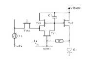
図1は、従来のアクティブマトリクス型表示装置における1つの画素10に対応する最も基本的な回路構成を示しており、これはコンダクタンスコントロール方式と呼ばれている。図1においてNチャンネルで構成された制御用TFT(Tr1)のゲートGは、走査ドライバー1からの走査ライン1aに接続され、そのソースSはデータドライバー2からのデータライン2aに接続されている。また、制御用TFT(Tr1)のドレインDは、Pチャンネルで構成された駆動用TFT(Tr2)のゲートGに接続されると共に、電荷保持用のコンデンサC1 の一方の端子に接続されている。
【0005】
そして、駆動用TFT(Tr2)のソースSは前記コンデンサC1 の他方の端子に接続されると共に、発光素子としての有機EL素子E1 に駆動電流を供給する陽極側電源(VHanod)に接続されている。また、駆動用TFT(Tr2)のドレインDは前記EL素子E1 の陽極に接続され、当該EL素子の陰極は、陰極側電源(VLcath)に接続されている。
【0006】
図1における制御用TFT(Tr1)のゲートに走査ライン1aを介してオン制御電圧(Select)が供給されると、制御用TFT(Tr1)はソースに供給されるデータライン2aからのデータ電圧(Vdata)に対応した電流を、ソースからドレインに流す。したがって、制御用TFT(Tr1)のゲートがオン電圧の期間に、前記コンデンサC1 が充電され、その電圧が駆動用TFT(Tr2)のゲートに供給される。それ故、駆動用TFT(Tr2)は、そのゲート電圧とソース電圧に基づいた電流をEL素子E1 に流し、EL素子を発光駆動させる。
【0007】
また制御用TFT(Tr1)のゲートがオフ電圧になると、制御用TFT(Tr1)はいわゆるカットオフとなり、制御用TFT(Tr1)のドレインは開放状態となるものの、駆動用TFT(Tr2)はコンデンサC1 に蓄積された電荷によりゲート電圧が保持され、次の走査まで駆動電流を維持し、EL素子E1 の発光も維持される。
【0008】
前記した構成はコンダクタンスコントロール方式による1つの画素10の接続構成例を示したものであり、この画素10の構成は縦および横方向に多数配列され、画像信号に基づいて各画素10が点灯または消灯制御されることで、映像が再生されることになる。
【0009】
ところで、この種のアクティブマトリクス型表示パネルにおいては、各画素内のTFTおよびコンデンサの不良は画素欠陥となる。表示パネル内に幾つかの欠陥が生ずることはやむを得ないのが現状であるものの、この欠陥数が多くなると、表示品位を落とし商品としては不適格となる。
【0010】
したがって、前記TFTおよび電荷保持用のコンデンサを基板に形成させた状態、すなわち、発光素子としての有機EL素子を前記基板に成膜させる以前の半製品の状態で前記TFTおよび電荷保持用のコンデンサの欠陥を容易に検査することができれば、表示パネルの歩留まりを改善することができ、結果としてコストの削減に寄与することができる。特に画素毎のTFTが1個で済むAM−LCD(アクティブマトリクス型液晶表示装置)に比べて、画素毎のTFTが2個〜4個以上必要となるAM−OEL(アクティブマトリクス型有機EL表示装置)においては、前記した半製品の状態での欠陥の検査はなおさら重要となる。
【0011】
一方、AM−LCDにおいては、前記した半製品の状態であるTFT基板状態においても電荷保持用コンデンサが画素用TFT(駆動用TFT)の負荷となっているために、TFT基板状態での画素欠陥の検査は比較的容易である。しかしながら、AM−OELにおいては前記した半製品の状態のTFT基板においては有機EL素子が成膜されておらず、駆動用TFTは無負荷状態である。したがって、この様な状態では画素欠陥の検査は容易ではない。
【0012】
そこで、画素欠陥を検査するためにプローブを所定の絵素電極等に当てて、インピーダンスを測定することが特許文献1に提案されており、したがって、同様に発光素子としての前記EL素子が形成される電極に、導電性のピン等を接触させるなどして、駆動用TFTに負荷を接続し、画素欠陥の検査をすることが考えられる。
【0013】
【特許文献1】
特許第2506840号公報(第2欄15行以降、および第6図)
【0014】
【発明が解決しようとする課題】
ところで、前記したように画素欠陥の検査工程において、発光素子としての前記EL素子が形成される電極に導電性のピン等を接触させるような作業がなされた場合においては、前記電極を損傷させる等して発光素子の不良を招来させる可能性が増大し、好ましくはない。また、発光素子が形成される電極に検査用の電極を近づけ、両電極間でコンデンサを形成することで、非接触状態で駆動用TFTに負荷を与える手段を採用することも考えられるが、両電極間のギャップ調整が極めて難しく、実用上においては採用し兼ねる。
【0015】
この発明は、前記した問題点を解消するためになされたものであり、たとえば半製品の状態で、検査用ダミー負荷を基板に形成させておき、これを利用することで、前記したTFTおよび電荷保持用コンデンサの欠陥検査を実行することができるアクティブ駆動型画素構造およびその検査方法を提供することを課題とするものである。
【0016】
【課題を解決するための手段】
前記した課題を解決するためになされたこの発明にかかる第1形態のアクティブ駆動型画素構造は、請求項1に記載のとおり、データラインの電位に基づいて制御出力を生成する制御用TFTと、前記制御出力に基づいて駆動電流が制御される駆動用TFTと、前記制御出力を一時的に保持する電荷保持用コンデンサとを少なくとも備えたアクティブ駆動型画素構造であって、前記駆動用TFTの電流出力端子に検査用ダミー負荷の一端が接続されると共に、当該検査用ダミー負荷の他端が検査用ラインに接続されている点に特徴を有する。
【0017】
また、この発明にかかる第2形態のアクティブ駆動型画素構造は、請求項2に記載のとおり、データラインの電位に基づいて制御出力を生成する制御用TFTと、前記制御出力に基づいて駆動電流が制御される駆動用TFTと、前記制御出力を一時的に保持する電荷保持用コンデンサとを少なくとも備えたアクティブ駆動型画素構造であって、前記駆動用TFTの電流出力端子に検査用ダミー負荷の一端が接続されると共に、当該検査用ダミー負荷の他端が前記駆動用TFTのゲートに接続されている点に特徴を有する。
【0018】
さらに、この発明にかかる第3形態および第4形態のアクティブ駆動型画素構造は、請求項3に記載のとおり、データラインの電位に基づいて制御出力を生成する制御用TFTと、前記制御出力に基づいて駆動電流が制御される駆動用TFTと、前記制御出力を一時的に保持する電荷保持用コンデンサとを少なくとも備えたアクティブ駆動型画素構造であって、前記駆動用TFTの電流出力端子に検査用ダミー負荷の一端が接続されると共に、当該検査用ダミー負荷の他端が前記制御用TFTのソースまたはゲートに接続されている点に特徴を有する。
【0019】
一方、前記した課題を解決するためになされたこの発明にかかる第1態様のアクティブ駆動型画素構造の検査方法は、請求項4に記載のとおり、データラインの電位に基づいて制御出力を生成する制御用TFTと、前記制御出力に基づいて駆動電流が制御される駆動用TFTと、前記制御出力を一時的に保持する電荷保持用コンデンサとが少なくとも備えられ、前記駆動用TFTの電流出力端子に検査用ダミー負荷の一端が接続されると共に、当該検査用ダミー負荷の他端が検査用ラインに接続されてなるアクティブ駆動型画素構造の検査方法であって、前記制御用TFTをオン状態にするステップと、前記駆動用TFTのゲート電圧、ソース電圧、検査用ラインのライン電圧のいずれか、もしくは2つ以上を相対的に変化させながら、前記検査用ダミー負荷に流れる電流値を測定するステップとを実行する点に特徴を有する。
【0020】
また、この発明にかかる第2態様のアクティブ駆動型画素構造の検査方法は、請求項5に記載のとおり、データラインの電位に基づいて制御出力を生成する制御用TFTと、前記制御出力に基づいて駆動電流が制御される駆動用TFTと、前記制御出力を一時的に保持する電荷保持用コンデンサとが少なくとも備えられ、前記駆動用TFTの電流出力端子に検査用ダミー負荷の一端が接続されると共に、当該検査用ダミー負荷の他端が前記駆動用TFTのゲートに接続されてなるアクティブ駆動型画素構造の検査方法であって、前記制御用TFTをオン状態にするステップと、前記駆動用TFTのゲート電圧、またはソース電圧のいずれか、もしくは2つを相対的に変化させながら、前記検査用ダミー負荷に流れる電流値を測定するステップとを実行する点に特徴を有する。
【0021】
さらに、この発明にかかる第3態様および第4態様のアクティブ駆動型画素構造の検査方法は、請求項6に記載のとおり、データラインの電位に基づいて制御出力を生成する制御用TFTと、前記制御出力に基づいて駆動電流が制御される駆動用TFTと、前記制御出力を一時的に保持する電荷保持用コンデンサとが少なくとも備えられ、前記駆動用TFTの電流出力端子に検査用ダミー負荷の一端が接続されると共に、当該検査用ダミー負荷の他端が前記制御用TFTのソースまたはゲートに接続されてなるアクティブ駆動型画素構造の検査方法であって、前記制御用TFTをオン状態にするステップと、前記駆動用TFTのゲート電圧、ソース電圧、または検査用ダミー負荷の他端の電圧のいずれか、もしくは2つ以上を相対的に変化させながら、前記検査用ダミー負荷に流れる電流値を測定するステップとを実行する点に特徴を有する。
【0022】
そして、この発明にかかるアクティブ駆動型画素構造の検査方法においては、請求項7に記載のとおり、検査用ダミー負荷は、当該検査用ダミー負荷に流れる電流値を測定するステップの実行後に、ハイインピーダンスの状態となるように処理される。
【0023】
【発明の実施の形態】
以下、この発明にかかるアクティブ駆動型画素構造およびその検査方法について、図に示す実施の形態に基づいて説明する。なお、以下の説明においては、すでに説明した図1に示された各部に相当する部分を同一符号で示しており、したがって個々の機能および動作については適宜説明を省略する。
【0024】
まず、図2はこの発明にかかるアクティブ駆動型画素構造の第1の形態を示したものである。この図2に示す形態は図1に示した例と同様にコンダクタンスコントロール方式と呼ばれる回路構成を示している。そして、図2に示す状態は有機EL素子E1 が成膜される前の半製品の状態を示している。
【0025】
図2に示す第1の形態においては、駆動用TFT(Tr2)の電流出力端子であるドレインに検査用ダミー負荷Wの一端が接続されると共に、当該ダミー負荷Wの他端が検査用ライン3に接続された構成とされている。すなわち、図1に示した構成と比較すると、検査用ダミー負荷Wおよび検査用ライン3が新たに備えられている。そして、後述するように、検査用ライン3と陰極側電源(VLcath)との間に、電流測定手段が介在され、ダミー負荷Wに流れる電流値を測定することで、各TFT(Tr1,Tr2)および電荷保持用コンデンサC1 の機能が正常であるか否かが検査される。すなわち、この実施の形態においてはダミー負荷Wに流れる電流値を、検査用ライン3を介して測定するようになされる。
【0026】
ここで、前記したコンダクタンスコントロール方式の回路構成における各部の電位を考察すると、まずEL素子E1 を発光駆動するには15V程度の電位差が必要である。そして、基準電位(アース電位)に対してなるべく低電圧で駆動動作を実現させるために、実用上においては、EL素子の陽極側電源(VHanod)として、たとえば10V、EL素子の陰極側電源(VLcath)として、たとえば−5Vを設定するなどの設計がなされる。
【0027】
前記した電圧設定条件において、駆動用TFT(Tr2)をオン・オフ制御させるに必要な駆動用TFTのゲート電圧を考えた場合、駆動用TFTはPチャンネルであるため、これをオフ状態にするには最低で10Vの電位が必要になる。また駆動用TFTをオンさせるには、前記10Vよりも相当に低い電位、たとえばアース電位(=0V)を印加させることで制御できる。したがって、前記した条件によると、制御用TFT(Tr1)のソースに供給されるデータ信号電圧Vdataとしては、高レベル電位としてVHdata=10Vを、低レベル電位としてVLdata=0Vをそれぞれ設定することになる。
【0028】
一方、制御用TFT(Tr1)はNチャンネルであるため、前記VHdataおよびVLdataを選択的に駆動用TFT(Tr2)のゲートに供給するためには、制御用TFT(Tr1)のゲートには、VHdata=10Vに対して少なくとも2Vのスレッショルド電圧を加えた12Vの制御(選択)電圧を供給することが必要である。また、非走査時においては制御用TFT(Tr1)のゲートに、たとえばアース電位(=0V)を印加することで、当該制御用TFTをカットオフ状態にすることができる。
【0029】
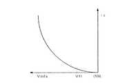
以上の考察に基づき、図2に示す形態において画素機能の検査を実行するには、まず、走査ライン1aに制御用TFT(Tr1)がオン状態になり得る電位、すなわち前記した12Vを印加させる。この状態で、データライン2aの電位を10V(=VHanod)から除々に低下させる(スイープさせる)と、駆動用TFT(Tr2)は除々にオン状態に移行する。なお、図3は駆動用TFTが除々にオン状態に移行する様子を示している。
【0030】
すなわち、図3に示す横軸はデータライン2a(制御用TFTのソース)に加わる電位を示しており、左方向に移行するにしたがってVdataとして示した電位は10Vから低下する状態で示している。また、図3に示す縦軸は駆動用TFT(Tr2)のドレインから、ダミー負荷Wおよび検査用ライン3を介して陰極側電源(VLcath)に流れる電流値Id を示している。したがって、この図3に示す特性は、駆動用TFT(Tr2)のId −Vgs特性(ドレイン電流−ゲート・ソース間電圧特性)にほぼ等しいものとなる。
【0031】
なお、検査用ライン3を介して流れる前記電流Id は、特に図示していないが、検査用ライン3と陰極側電源(VLcath)との間に介在された電流測定手段により得ることができる。したがって、データライン電圧(Vdata)に関係なく検査用ライン3に電流が流れたり、逆に検査用ライン3に電流が流れたままの状態である場合には、前記TFT(Tr1,Tr2)またはコンデンサC1 のいずれかが不良であることが判る。また、所定のId 値が流れるVgs値(=Vth:スレッショルド電圧)が規定の電圧を超える状態であるならば、駆動用TFT(Tr2)が不良であることが判る。
【0032】
以上のようにして各画素毎に評価し、1パネル内の不良画素が規定数以内ならば良品、規定数を超えるならば不良品と判定する。このようにして検査が終了したならば、各駆動用TFTに接続されたダミー負荷Wは、ハイインピーダンスの状態となるように処理される。すなわち、前記ダミー負荷WはEL素子を成膜し、発光表示パネルを形成した場合においては、電気的に短絡状態を引き起こすことになるので、前記した処理を実行することで、このダミー負荷を無効にする処置がなされる。
【0033】
前記ダミー負荷Wをハイインピーダンスの状態となるように処理する一例としては、レーザビームにより検査用ダミー負荷を破壊する(焼き切る)ことが考えられる。これにより、各駆動用TFTのドレインと検査用ライン3との電気的な接続は開放される。また、後で説明する実施の形態において詳述するが、検査用ダミー負荷Wに所定の電流を流すことで、当該検査用ダミー負荷を溶断する手段も好適に採用することもできる。一方、前記した検査用ダミー負荷Wは、単なるワイヤーや抵抗体の他、所定電流以上が流れると溶断するいわゆるヒューズと同様の機能を備えた素子や、TFT或いはダイオードのような素子であってもよい。
【0034】
なお、以上説明した第1の実施の形態における検査方法においては、データライン2aの電位Vdataを変化させること、換言すれば駆動用TFT(Tr2)のゲート電圧を変化させることで、ダミー負荷Wに流れる電流Id 、すなわち、検査用ライン3に流れる電流Id を測定するようにしている。しかしながら、検査用ライン3に印加されるライン電圧(VLcath)、または駆動用TFT(Tr2)のソースに供給される駆動電圧(VHanod)を単独に変化させても、もしくは前記2つ以上を相対的に変化させても、図3に示したような駆動用TFTのI−V(電流−電圧)特性を得ることができ、これによっても、前記と同様に各画素のTFT(Tr1,Tr2)またはコンデンサC1 の機能が正常であるか否かを検査することができる。
【0035】
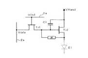
次に図4は、この発明にかかるアクティブ駆動型画素構造の第2の形態を示したものである。この図4に示す形態も同様にコンダクタンスコントロール方式と呼ばれる回路構成を示している。そして、図4に示す状態は同様に有機EL素子E1 が成膜される前の半製品の状態を示している。この第2の形態においては、駆動用TFT(Tr2)の電流出力端子であるドレインに、検査用ダミー負荷Wの一端が接続されると共に、当該ダミー負荷の他端は駆動用TFT(Tr2)のゲートに接続されている。
【0036】
そして、データライン2aとこのデータライン2aにデータライン電圧(Vdata)をもたらす図示せぬ電圧源(図1に示すデータドライバー2に代わるもの)との間に、電流測定手段が介在され、データライン2aに流れる電流値を測定するようになされる。この場合のデータライン電流は、駆動用TFT(Tr2)のドレイン電流Id が、ダミー負荷Wおよび制御用TFT(Tr1)を介して得られるものであり、前記データライン電流は、結果として駆動用TFT(Tr2)のドレイン電流Id にほぼ対応するものとなる。
【0037】
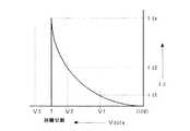
図4に示す画素構成において、その検査を実行するには、図2に示した第1の形態と同様に、走査ライン1aに制御用TFT(Tr1)がオン状態になり得る電圧、たとえば12Vを印加させる。この状態で、データライン2aの電圧を順にV1 ,V2 ,V3 と変化させる。すなわち、前記V1 ,V2 ,V3 の各値は、駆動用TFT(Tr2)がカットオフ状態となる10V(=VHanod)よりも低レベルの範囲で、その電圧レベルが順に低下するように変更される。図5はこの時のデータライン電流(駆動用TFTのドレイン電流Id )の変化状態を示している。なお、この特性はすでに説明した図3に示すものと同様のものである。
【0038】
図5に示すようにデータライン2aの電圧としてV1 を与えた時の電流値Id1の値、およびデータライン2aの電圧としてV2 を与えた時の電流値Id2の値が測定され、この電流値Id1,Id2がそれぞれ規定の範囲内であるならばTFT(Tr1,Tr2)およびコンデンサC1 の機能は正常であると判定される。なお、この実施の形態においては、前記ダミー負荷Wとして所定の電流値Idx以上の電流が流れた時に溶断するいわゆるヒューズと同様の機能を備えた素子が採用されている。
【0039】
そして、図5に示すようにデータライン2aに対してV3 が与えられる。このV3 として示す電位は、駆動用TFT(Tr2)のゲートバイアスとして与えられ、この時のドレイン電流は、前記Idx以上の電流が流れる値に設定されている。したがって、前記ダミー負荷Wは駆動用TFTのドレイン電流により溶断される。この時、前記ドレイン電流Id がほぼゼロになるか否かがデータライン2aを介して確認され、以上の工程によって各画素毎の良否が判定される。そして、パネル毎の良否の判断は、図2および図3に基づいて説明した実施の形態と同様になされる。
【0040】
なお、以上説明した第2の実施の形態における検査方法においては、データライン2aの電位Vdataを変化させること、換言すれば駆動用TFT(Tr2)のゲート電圧を変化させることで、ダミー負荷Wに流れる電流Id を、データライン2aにおいて測定するようにしている。しかしながら、この実施の形態においては、駆動用TFT(Tr2)のソースに供給される駆動電圧VHanodを変化させても、もしくは前記データライン2aの電位Vdataと駆動電圧VHanodの双方を相対的に変化させても、図5に示したような駆動用TFTのI−V(電流−電圧)特性を取得することができる。したがって、このような手段を採用しても前記と同様に各画素のTFT(Tr1,Tr2)またはコンデンサC1 の機能が正常であるか否かを検査することができる。
【0041】
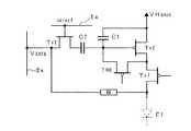
図6は、この発明にかかるアクティブ駆動型画素構造の第3の形態を示したものである。この図6に示す形態も同様にコンダクタンスコントロール方式と呼ばれる回路構成を示している。そして、図6に示す状態は同様に有機EL素子E1 が成膜される前の半製品の状態を示している。この第3の形態においては、駆動用TFT(Tr2)の電流出力端子であるドレインに、検査用ダミー負荷Wの一端が接続されると共に、当該ダミー負荷の他端は制御用TFT(Tr1)のソースに接続されている。
【0042】
この例においても、図4に示した例と同様にデータライン2aとこのデータライン2aにデータライン電圧Vdataをもたらす図示せぬ電圧源との間に、電流測定手段が介在され、データライン2aに加えるデータ電圧Vdataに対応するデータライン2aに流れる電流値を測定するようになされる。すなわち、データライン2aに流れる電流値は、図4に示した例と同様に駆動用TFT(Tr2)のドレイン電流Id に対応するものであり、データ電圧Vdataとドレイン電流Id との関係を対比することによって、各画素のTFT(Tr1,Tr2)またはコンデンサC1 の機能が正常であるか否かを検査することができる。
【0043】
そして、前記した測定が終了した場合には、検査用ダミー負荷Wはレーザビームにより破壊する(焼き切る)か、またはダミー負荷に所定の電流を流すことで、当該検査用ダミー負荷を溶断するようになされる。この、図6に示す形態においても、駆動電圧VHanodを変化させることで、駆動用TFTのI−V(電流−電圧)特性を取得することができる。したがって、このような手段を採用しても前記と同様に各画素のTFT(Tr1,Tr2)またはコンデンサC1 の機能が正常であるか否かを検査することができる。
【0044】
なお、図6に示した実施の形態によると、図4に示した実施の形態に比較して制御用TFT(Tr1)を介さずに、データライン2aにおいて駆動用TFTのドレイン電流Id を実質的に得ることができる。したがって、この図6に示した実施の形態によると、制御用TFT(Tr1)として格別に電流容量の高いTFTを形成させる必要はないという利点が得られる。
【0045】
図7は、この発明にかかるアクティブ駆動型画素構造の第4の形態を示したものである。この図7に示す形態も同様にコンダクタンスコントロール方式と呼ばれる回路構成を示している。そして、図7に示す状態は同様に有機EL素子E1 が成膜される前の半製品の状態を示している。この第4の形態においては、駆動用TFT(Tr2)の電流出力端子であるドレインに、検査用ダミー負荷Wの一端が接続されると共に、当該ダミー負荷の他端は制御用TFT(Tr1)のゲートに接続されている。
【0046】
この例においては、走査ライン1a とこの走査ライン1aに制御(選択)電圧をもたらす図示せぬ電圧源(図1に示す走査ドライバー1に代わるもの)との間に、図示せぬ電流測定手段が介在され、走査ライン1a に流れる電流値を測定するようになされる。この場合の走査ライン1a に流れる電流は、駆動用TFT(Tr2)のドレイン電流Id が、ダミー負荷Wを介して得られるものであり、前記走査ライン1a に得られる電流は、結果として駆動用TFT(Tr2)のドレイン電流Id にほぼ対応するものとなる。
【0047】
なお、この図7に示す実施の形態においては、データライン2aに加えるデータ電圧Vdataに対応する走査ライン1aに流れる電流値(実質的に駆動用TFTのドレイン電流Id )を測定するようになされ、データ電圧Vdataとドレイン電流Id との関係を対比することによって、各画素のTFT(Tr1,Tr2)またはコンデンサC1 の機能が正常であるか否かが検査される。
【0048】
この場合、走査ライン1aに対して制御用TFT(Tr1)がオン状態となる電圧、たとえば前記した12Vを常時印加した場合には、電位差の関係で走査ライン1aにおいて、駆動用TFTのドレイン電流Id を検出することが不可能になる。そこで、走査ライン1aを介して制御用TFT(Tr1)のゲートに加えるオン電圧は、データライン2aに加えるデータ電圧Vdataに対応させて可変させるように制御することが必要となる。
【0049】
そして、前記した測定が終了した場合には、検査用ダミー負荷Wはレーザビームにより破壊する(焼き切る)か、またはダミー負荷に所定の電流を流すことで、当該検査用ダミー負荷を溶断するようになされる。この図7に示す形態においても、駆動電圧VHanodを変化させることで、駆動用TFTのI−V(電流−電圧)特性を取得することができる。したがって、このような手段を採用しても前記と同様に各画素のTFT(Tr1,Tr2)またはコンデンサC1 の機能が正常であるか否かを検査することができる。
【0050】
なお、図7に示した実施の形態によると、図4に示した実施の形態に比較して制御用TFT(Tr1)を介さずに、データライン2aにおいて駆動用TFTのドレイン電流Id を実質的に得ることができる。したがって、この図7に示した実施の形態においても、制御用TFT(Tr1)として格別に電流容量の高いTFTを形成させる必要はないという利点が得られる。
【0051】
次に図8は、図7に示した構成において、さらに駆動用TFT(Tr2)のソース・ドレイン間にダイオード素子を並列接続したものである。すなわち、ダイオード素子を前記のとおり並列接続することによりEL素子E1 に対して逆バイアス電圧を効果的に印加できるようにした構成に、この発明を採用した例を示している。なお、図8に示す例においてはダイオード素子としてTFT(Tr3)が用いられており、そのゲートとソースを短絡することにより、等価的にダイオード素子を形成している。
【0052】
この様にダイオード素子を配置し、所定のタイミングにおいて、たとえば駆動電圧源VHanod,VLcathを入れ替えることで、前記ダイオード素子を介してEL素子E1 に対して逆バイアス電圧を効果的に印加することができ、これにより、EL素子の寿命を延ばすことができる。なお、この図8に示す逆バイアスの印加手段は、本件出願人において特願2002−230072として出願している。したがって、図8に示した構成においても、図7に示した構成例と同様の本件発明による作用効果を得ることができる。
【0053】
図9は、デジタル階調を実現させる3TFT方式の画素構成に対してこの発明を適用した例を示す。この駆動方式はSES(Simultaneous−Erasing−Scan =同時消去法)とも呼ばれており、制御用TFT(Tr1)と、駆動用TFT(Tr2)に加えて、消去用TFT(Tr4)が備えられている。この消去用TFT(Tr4)は、EL素子E1 点灯期間の途中において、当該消去用TFT(Tr4)をオン動作させることで、コンデンサC1 の電荷を放電させることができ、これによりEL素子E1 の点灯期間を制御する階調駆動を実現させることができる。
【0054】
この図9に示した構成においても、図6に示した例と同様に、駆動用TFT(Tr2)の電流出力端子であるドレインに、検査用ダミー負荷Wの一端が接続されると共に、当該ダミー負荷の他端は制御用TFT(Tr1)のソースに接続されている。したがって、この図9に示した構成においても、図6に基づいて説明した作用効果と同様の作用効果を得ることができる。
【0055】
図10は電流プログラミング方式の画素構成に対してこの発明を適用した例を示している。この電流プログラミング方式においては、駆動用TFT(Tr2)のドレインにスイッチング用TFT(Tr5)が接続され、このスイッチング用TFT(Tr5)のドレインにEL素子E1 が形成されるようになされる。そして、駆動用TFT(Tr2)のソースとゲート間に電荷保持用のコンデンサC1 が接続され、駆動用TFT(Tr2)のゲートとドレインとの間には制御用TFT(Tr1)が接続されている。
【0056】
さらに制御用TFT(Tr1)のソースには書き込み用電流源Is が接続されている。加えて、制御用TFT(Tr1)とスイッチング用TFT(Tr5)の各ゲートは走査ライン1a に接続されており、前記書き込み用電流源Is はデータ線2a における電流を制御するように機能する。
【0057】
図10に示した構成においては、スイッチング用TFT(Tr5)のドレインに検査用ダミー負荷Wの一端が接続されると共に、当該ダミー負荷の他端は制御用TFT(Tr1)のゲートに接続されている。したがって、この構成によるとダミー負荷Wにはスイッチング用TFT(Tr5)を介して駆動用TFT(Tr2)のドレイン電流Id が流れ、このドレイン電流Id は走査ライン1a によって測定することができる。それ故、この図10に示した構成においても、図7に基づいて説明した作用効果と同様の作用効果を得ることができる。
【0058】
次に図11は、スレッショルド電圧補正方式と呼ぶことにし、このスレッショルド電圧補正方式の画素構成に対してこの発明を適用した例を示している。この図11に示したスレッショルド電圧補正方式の基本構成は、図7に示したコンダクタンスコントロール方式と同様であり、コンダクタンスコントロール方式に比較すると、制御用TFT(Tr1) と駆動用TFT(Tr2)との間に、TFT(Tr6)とダイオードD1 との並列接続体が挿入されている。なお、前記TFT(Tr6)はそのゲート・ドレイン間は短絡状態に構成されており、したがって、これは制御用TFT(Tr1) から駆動用TFT(Tr2)のゲートに向かってスレッショルド特性を与える素子として機能する。
【0059】
この構成によると、駆動用TFT(Tr2)におけるスレッショルド特性を、TFT(Tr6)によって生成されるスレッショルド特性によって効果的にキャンセルさせることができる。そして、この実施の形態においても、駆動用TFT(Tr2)のドレインに検査用ダミー負荷Wの一端が接続されると共に、当該ダミー負荷の他端は制御用TFT(Tr1)のゲートに接続されている。
【0060】
したがって、この図11に示す構成においても、駆動用TFT(Tr2)におけるドレイン電流Id は、走査ライン1a によって測定することができる。それ故、この図11に示した構成においても、図7に基づいて説明した作用効果と同様の作用効果を得ることができる。
【0061】
図12は、電圧プログラミング方式の画素構成に対してこの発明を適用した例を示している。この電圧プログラミング方式においては、駆動用TFT(Tr2)のドレインに対してスイッチング用TFT(Tr7)が接続されており、また駆動用TFT(Tr2)のドレインとゲートとの間にスイッチング用TFT(Tr8)が接続されている。
【0062】
加えてこの電圧プログラミング方式においては、駆動用TFT(Tr2)のゲートに対して、データライン2a より制御用TFT(Tr1)およびコンデンサC2 を介してデータ信号が供給されるように構成されている。
【0063】
前記した電圧プログラミング方式においては、TFT(Tr7) およびTFT(Tr8)がオンされ、これに伴い駆動用TFT(Tr2)のオン状態が確保される。次の瞬間にTFT(Tr7)がオフされることにより、駆動用TFT(Tr2)のドレイン電流Id はTFT(Tr8) を介して駆動用TFT(Tr2)のゲートに回り込む。これにより、駆動用TFT(Tr2)のゲート・ソース間電圧が、駆動用TFTのスレッショルド電圧に等しくなるまで、ゲート・ソース間電圧が押し上げられ、この時点で駆動用TFT(Tr2)はオフする。
【0064】
そして、この時のゲート・ソース間電圧がコンデンサC1 に保持され、このコンデンサ電圧によって、駆動用TFTのドレイン電流が制御される。すなわち、この電圧プログラミング方式においては、駆動用TFT(Tr2)におけるスレッショルド電圧のばらつきを補償するように作用する。
【0065】
前記した図12に示す構成においては、TFT(Tr7) のドレインに検査用ダミー負荷Wの一端が接続されると共に、当該ダミー負荷の他端は制御用TFT(Tr1)のソースに接続されている。したがって、駆動用TFT(Tr2)のドレイン電流Id は、TFT(Tr7) およびダミー負荷Wを介してデータライン2a において検出することができる。それ故、この図12に示した構成においても、図6に基づいて説明した作用効果と同様の作用効果を得ることができる。
【0066】
図13は、カレントミラー方式の画素構成に対してこの発明を適用した例を示している。このカレントミラー方式においては、Pチャンネルの駆動用TFT(Tr2)にゲートが共通接続されて同じくPチャンネルのTFT(Tr9)が対称的に備えられており、両TFT(Tr2,Tr9)のゲートとソース間に電荷保持用のコンデンサC1 が接続されている。
【0067】
また、前記TFT(Tr9)のゲートとドレイン間には制御用TFT(Tr1)が接続されており、この制御用TFT(Tr1)のオン動作により、TFT(Tr2,Tr9)はカレントミラーとして機能する。すなわち、制御用TFT(Tr1)のオン動作と共にNチャンネルにより構成されたスイッチング用TFT(Tr10 )もオン動作されるように構成されており、これにより、スイッチング用TFT(Tr10 )を介して書き込み用電流源Is が接続されるように構成されている。
【0068】
これにより、アドレス期間においてはVHanodの電源から、TFT(Tr9)、TFT(Tr10 )を介して書き込み用電流源Is に流れる電流経路が形成され、また、カレントミラーの作用により、電流源Is に流れる電流に対応した電流が、駆動用TFT(Tr2)のドレイン電流Id として生成される。
【0069】
このような動作によりコンデンサC1 には書き込み用電流源Is に流れる電流値に対応したTFT(Tr9)のゲート電圧が書き込まれる。そして、コンデンサC1 に所定の電圧値が書き込まれた後には、制御用TFT(Tr1)はオフ状態になされ、駆動用TFT(Tr2)は、コンデンサC1 に蓄積された電荷に基づいて所定のドレイン電流Id を供給するように作用する。
【0070】
そして、図13に示す実施の形態においては、駆動用TFT(Tr2)の電流出力端子であるドレインに、検査用ダミー負荷Wの一端が接続されると共に、当該ダミー負荷の他端は制御用TFT(Tr1)のゲートに接続されている。したがって、この図13に示す構成においても、駆動用TFT(Tr2)におけるドレイン電流Id は、走査ライン1a によって測定することができる。それ故、この図13に示した構成においても、図7に基づいて説明した作用効果と同様の作用効果を得ることができる。
【図面の簡単な説明】
【図1】従来のアクティブマトリクス型表示装置における1つの画素に対応する基本的な回路構成を示した結線図である。
【図2】この発明にかかるアクティブ駆動型画素構造の第1の形態を示した結線図である。
【図3】図2に示す構成における駆動用TFTの動作を示す特性図である。
【図4】この発明にかかるアクティブ駆動型画素構造の第2の形態を示した結線図である。
【図5】図4に示す構成における駆動用TFTの動作を示す特性図である。
【図6】この発明にかかるアクティブ駆動型画素構造の第3の形態を示した結線図である。
【図7】同じく第4の形態を示した結線図である。
【図8】EL素子に逆バイアス電圧を効果的に印加できるように構成した画素構成に対してこの発明を適用した例を示す結線図である。
【図9】SES方式の画素構成に対してこの発明を適用した例を示す結線図である。
【図10】電流プログラミング方式の画素構成に対してこの発明を適用した例を示す結線図である。
【図11】スレッショルド電圧補正方式の画素構成に対してこの発明を適用した例を示す結線図である。
【図12】電圧プログラミング方式の画素構成に対してこの発明を適用した例を示す結線図である。
【図13】カレントミラー方式の画素構成に対してこの発明を適用した例を示す結線図である。
【符号の説明】
1 走査ドライバー
1a 走査ライン
2 データドライバー
2a データライン
3 検査用ライン
10 画素
C1 ,C2 コンデンサ
D1 ダイオード
E1 発光素子(有機EL素子)
Is 書き込み用電流源
Tr1 制御用TFT
Tr2 駆動用TFT
W 検査用ダミー負荷[0001]
TECHNICAL FIELD OF THE INVENTION
The present invention relates to an active drive pixel structure including at least a control TFT, a drive TFT, and a charge holding capacitor, and a method for inspecting the active drive pixel structure. The present invention relates to an active drive type pixel structure that enables easy inspection of whether or not the functions of a TFT (Thin Film Transistor) and a charge holding capacitor are normal, and an inspection method thereof.
[0002]
[Prior art]
2. Description of the Related Art A display using a display panel configured by arranging light-emitting elements in a matrix has been widely developed. As a light emitting element used for such a display panel, an organic EL (electroluminescence) element using an organic material for a light emitting layer has attracted attention. This is due to the fact that the use of an organic compound that can be expected to have good light-emitting characteristics in the light-emitting layer of the EL element has promoted high efficiency and long life that can be put to practical use.
[0003]
As a display panel using such an organic EL element, a simple matrix type display panel in which EL elements are simply arranged in a matrix, and an active matrix type display in which an active element composed of a TFT is added to each of the EL elements arranged in a matrix. A panel has been proposed. The latter active matrix display panel has characteristics such as lower power consumption and less crosstalk between pixels than the former simple matrix display panel. Suitable for high definition displays.
[0004]
FIG. 1 shows the most basic circuit configuration corresponding to one
[0005]
The source S of the driving TFT (Tr2) is connected to the other terminal of the capacitor C1 and to the anode-side power supply (VHanod) for supplying a driving current to the organic EL element E1 as a light emitting element. . The drain D of the driving TFT (Tr2) is connected to the anode of the EL element E1, and the cathode of the EL element E1 is connected to the cathode side power supply (VLcat).
[0006]
When an on-control voltage (Select) is supplied to the gate of the control TFT (Tr1) in FIG. 1 via the scanning line 1a, the control TFT (Tr1) supplies the data voltage (Data) from the
[0007]
When the gate of the control TFT (Tr1) is turned off, the control TFT (Tr1) is cut off, and the drain of the control TFT (Tr1) is open, but the drive TFT (Tr2) is a capacitor. The gate voltage is held by the charge accumulated in C1, the drive current is maintained until the next scan, and the emission of the EL element E1 is also maintained.
[0008]
The above-described configuration is an example of a connection configuration of one
[0009]
In this type of active matrix display panel, defective TFTs and capacitors in each pixel become pixel defects. Although it is currently unavoidable that some defects occur in the display panel, when the number of defects increases, the display quality deteriorates and the display panel becomes ineligible.
[0010]
Therefore, in the state where the TFT and the capacitor for holding electric charge are formed on the substrate, that is, in the state of a semi-finished product before forming the organic EL element as a light emitting element on the substrate, the TFT and the capacitor for holding electric charge are formed. If defects can be easily inspected, the yield of the display panel can be improved, which can contribute to cost reduction. In particular, an AM-OEL (active matrix type organic EL display device) which requires two to four or more TFTs for each pixel as compared with an AM-LCD (active matrix type liquid crystal display device) which requires only one TFT for each pixel. In (2), inspection of defects in the state of the above-mentioned semi-finished product becomes even more important.
[0011]
On the other hand, in the AM-LCD, even in the TFT substrate state, which is a semi-finished product state, the charge holding capacitor loads the pixel TFTs (driving TFTs). Inspection is relatively easy. However, in the AM-OEL, the organic EL element is not formed on the TFT substrate in the semi-finished state, and the driving TFT is in a no-load state. Therefore, inspection of pixel defects is not easy in such a state.
[0012]
Therefore, it has been proposed in
[0013]
[Patent Document 1]
Japanese Patent No. 2506840 (
[0014]
[Problems to be solved by the invention]
By the way, as described above, in the pixel defect inspection process, when an operation such as contacting a conductive pin or the like with an electrode on which the EL element as a light emitting element is formed is performed, the electrode may be damaged. As a result, the possibility of causing a defect of the light emitting element increases, which is not preferable. It is also conceivable to use a means for bringing a load on the driving TFT in a non-contact state by bringing an inspection electrode close to the electrode on which the light emitting element is formed and forming a capacitor between the electrodes. It is extremely difficult to adjust the gap between the electrodes, and it is not used in practice.
[0015]
The present invention has been made in order to solve the above-described problems. For example, in the state of a semi-finished product, a dummy load for inspection is formed on a substrate, and by utilizing this, the above-described TFT and charge can be obtained. An object of the present invention is to provide an active drive type pixel structure capable of performing a defect inspection of a holding capacitor and an inspection method thereof.
[0016]
[Means for Solving the Problems]
According to a first aspect of the present invention, there is provided an active driving type pixel structure according to the present invention for solving the above-mentioned problem, comprising: a control TFT for generating a control output based on a potential of a data line; An active driving type pixel structure comprising at least a driving TFT whose driving current is controlled based on the control output, and a charge holding capacitor for temporarily holding the control output, wherein the current of the driving TFT is It is characterized in that one end of a test dummy load is connected to the output terminal, and the other end of the test dummy load is connected to a test line.
[0017]
According to a second aspect of the present invention, there is provided an active drive type pixel structure according to
[0018]
Further, according to the third and fourth forms of the active drive type pixel structure according to the present invention, a control TFT for generating a control output based on a potential of a data line and a control TFT for the control output are provided. An active driving type pixel structure including at least a driving TFT whose driving current is controlled based on the driving current, and a charge holding capacitor for temporarily holding the control output, wherein an inspection is performed on a current output terminal of the driving TFT. And the other end of the inspection dummy load is connected to the source or gate of the control TFT.
[0019]
On the other hand, an inspection method of an active drive type pixel structure according to a first aspect of the present invention which has been made to solve the above-described problem generates a control output based on a potential of a data line as described in claim 4. A control TFT, a drive TFT whose drive current is controlled based on the control output, and a charge holding capacitor for temporarily holding the control output, and at least a current output terminal of the drive TFT. An inspection method of an active drive pixel structure in which one end of an inspection dummy load is connected and the other end of the inspection dummy load is connected to an inspection line, wherein the control TFT is turned on. Step, while relatively changing any one or two or more of a gate voltage and a source voltage of the driving TFT, and a line voltage of a test line, Characterized in that it executes the steps of measuring the current flowing through the 査用 dummy load.
[0020]
According to a second aspect of the present invention, there is provided an inspection method of an active drive type pixel structure, wherein a control TFT for generating a control output based on a potential of a data line and a control TFT based on the control output are provided. At least a driving TFT whose driving current is controlled and a charge holding capacitor that temporarily holds the control output, and one end of a test dummy load is connected to a current output terminal of the driving TFT. A method for testing the active drive pixel structure in which the other end of the test dummy load is connected to the gate of the drive TFT, wherein the control TFT is turned on; Measuring the value of the current flowing through the inspection dummy load while relatively changing either the gate voltage or the source voltage, or both of them. Characterized in that the run.
[0021]
Further, according to the third aspect and the fourth aspect of the present invention, there is provided a method for inspecting an active drive type pixel structure, wherein a control TFT for generating a control output based on a potential of a data line, A drive TFT for controlling a drive current based on the control output; and a charge holding capacitor for temporarily holding the control output, wherein one end of a test dummy load is connected to a current output terminal of the drive TFT. Is connected, and the other end of the test dummy load is connected to a source or a gate of the control TFT, wherein the control TFT is turned on. And one or more of the gate voltage and the source voltage of the driving TFT or the voltage at the other end of the inspection dummy load are relatively changed. While, characterized in that it executes the steps of measuring the current flowing through the test dummy load.
[0022]
In the inspection method of the active drive pixel structure according to the present invention, as described in
[0023]
BEST MODE FOR CARRYING OUT THE INVENTION
Hereinafter, an active drive type pixel structure and an inspection method thereof according to the present invention will be described based on an embodiment shown in the drawings. In the following description, portions corresponding to the respective portions shown in FIG. 1 which have already been described are denoted by the same reference numerals, and therefore description of individual functions and operations will be appropriately omitted.
[0024]
First, FIG. 2 shows a first embodiment of the active drive type pixel structure according to the present invention. The embodiment shown in FIG. 2 shows a circuit configuration called a conductance control system, similarly to the example shown in FIG. The state shown in FIG. 2 shows the state of the semi-finished product before the organic EL element E1 is formed.
[0025]
In the first embodiment shown in FIG. 2, one end of the inspection dummy load W is connected to the drain, which is the current output terminal of the driving TFT (Tr2), and the other end of the dummy load W is connected to the inspection line 3. Connected to the system. That is, as compared with the configuration shown in FIG. 1, an inspection dummy load W and an inspection line 3 are newly provided. Then, as will be described later, a current measuring means is interposed between the inspection line 3 and the cathode side power supply (VLcath), and a current value flowing through the dummy load W is measured, whereby each TFT (Tr1, Tr2) is measured. It is checked whether the function of the charge holding capacitor C1 is normal. That is, in this embodiment, the value of the current flowing through the dummy load W is measured via the inspection line 3.
[0026]
Here, considering the potential of each part in the above-described circuit configuration of the conductance control method, first, a potential difference of about 15 V is necessary to drive the EL element E1 to emit light. In order to realize the driving operation at a voltage as low as possible with respect to the reference potential (earth potential), in practice, for example, 10 V is set as the anode side power supply (VHanod) of the EL element, and the cathode side power supply (VLcath) of the EL element is used. ) Is designed to set, for example, -5V.
[0027]
In consideration of the gate voltage of the driving TFT required to turn on / off the driving TFT (Tr2) under the above-described voltage setting conditions, the driving TFT is a P-channel. Requires a potential of at least 10V. Further, turning on the driving TFT can be controlled by applying a potential considerably lower than the above 10 V, for example, a ground potential (= 0 V). Therefore, according to the above conditions, as the data signal voltage Vdata supplied to the source of the control TFT (Tr1), VHdata = 10V is set as the high-level potential, and VLdata = 0V is set as the low-level potential. .
[0028]
On the other hand, since the control TFT (Tr1) has N channels, in order to selectively supply VHdata and VLdata to the gate of the driving TFT (Tr2), the gate of the control TFT (Tr1) needs to have VHdata. It is necessary to supply a control (selection) voltage of 12 V in which a threshold voltage of at least 2 V is added to = 10 V. In addition, at the time of non-scanning, for example, by applying a ground potential (= 0V) to the gate of the control TFT (Tr1), the control TFT can be cut off.
[0029]
Based on the above considerations, in order to execute the inspection of the pixel function in the embodiment shown in FIG. 2, first, a potential that can turn on the control TFT (Tr1), that is, the above-mentioned 12V is applied to the scanning line 1a. In this state, when the potential of the
[0030]
That is, the horizontal axis shown in FIG. 3 indicates the potential applied to the
[0031]
Although not shown, the current Id flowing through the test line 3 can be obtained by current measuring means interposed between the test line 3 and the cathode-side power supply (VLcath). Therefore, when a current flows through the inspection line 3 regardless of the data line voltage (Vdata), or when the current is still flowing through the inspection line 3, the TFT (Tr1, Tr2) or the capacitor It turns out that any of C1 is bad. Further, if the Vgs value (= Vth: threshold voltage) at which the predetermined Id value flows exceeds a specified voltage, it is determined that the driving TFT (Tr2) is defective.
[0032]
As described above, each pixel is evaluated, and if the number of defective pixels in one panel is within a specified number, it is determined as a good product, and if the number exceeds the specified number, it is determined as a defective product. When the inspection is completed in this way, the dummy load W connected to each driving TFT is processed so as to be in a high impedance state. That is, when the EL element is formed and the light emitting display panel is formed, the dummy load W causes an electrical short circuit state. Therefore, by executing the above-described processing, the dummy load is invalidated. Is performed.
[0033]
As an example of processing the dummy load W to be in a high impedance state, it is conceivable that the inspection dummy load is destroyed (burned out) by a laser beam. As a result, the electrical connection between the drain of each driving TFT and the inspection line 3 is released. Further, as will be described in detail in an embodiment described later, a means for blowing a predetermined current through the inspection dummy load W to blow the inspection dummy load can also be suitably employed. On the other hand, the above-described inspection dummy load W may be an element having a function similar to a so-called fuse that blows when a predetermined current or more flows, or an element such as a TFT or a diode, in addition to a simple wire or a resistor. Good.
[0034]
In the inspection method according to the first embodiment described above, by changing the potential Vdata of the
[0035]
Next, FIG. 4 shows a second embodiment of the active drive type pixel structure according to the present invention. The embodiment shown in FIG. 4 similarly shows a circuit configuration called a conductance control system. The state shown in FIG. 4 similarly shows the state of the semi-finished product before the organic EL element E1 is formed. In the second embodiment, one end of an inspection dummy load W is connected to a drain which is a current output terminal of the driving TFT (Tr2), and the other end of the dummy load is connected to the driving TFT (Tr2). Connected to the gate.
[0036]
A current measuring means is interposed between the
[0037]
In the pixel configuration shown in FIG. 4, in order to execute the inspection, a voltage at which the control TFT (Tr1) can be turned on, for example, 12 V, is applied to the scanning line 1a as in the first embodiment shown in FIG. Apply. In this state, the voltage of the
[0038]
As shown in FIG. 5, the value of the current value Id1 when V1 is given as the voltage of the
[0039]
Then, V3 is applied to the
[0040]
In the inspection method according to the second embodiment described above, by changing the potential Vdata of the
[0041]
FIG. 6 shows a third embodiment of the active drive type pixel structure according to the present invention. The embodiment shown in FIG. 6 similarly shows a circuit configuration called a conductance control system. The state shown in FIG. 6 similarly shows the state of the semi-finished product before the organic EL element E1 is formed into a film. In the third embodiment, one end of the inspection dummy load W is connected to the drain, which is the current output terminal of the driving TFT (Tr2), and the other end of the dummy load is connected to the control TFT (Tr1). Connected to source.
[0042]
Also in this example, similarly to the example shown in FIG. 4, current measuring means is interposed between the
[0043]
When the above-described measurement is completed, the inspection dummy load W is broken (burned out) by a laser beam or a predetermined current is applied to the dummy load to blow the inspection dummy load. Done. In the embodiment shown in FIG. 6, the IV (current-voltage) characteristics of the driving TFT can be obtained by changing the driving voltage VHanod. Therefore, even if such a means is adopted, it can be checked whether or not the function of the TFT (Tr1, Tr2) or the capacitor C1 of each pixel is normal as described above.
[0044]
According to the embodiment shown in FIG. 6, the drain current Id of the driving TFT is substantially reduced in the
[0045]
FIG. 7 shows a fourth embodiment of the active drive type pixel structure according to the present invention. The embodiment shown in FIG. 7 similarly shows a circuit configuration called a conductance control system. The state shown in FIG. 7 similarly shows the state of the semi-finished product before the organic EL element E1 is formed into a film. In the fourth embodiment, one end of a test dummy load W is connected to a drain, which is a current output terminal of a driving TFT (Tr2), and the other end of the dummy load is connected to a control TFT (Tr1). Connected to the gate.
[0046]
In this example, a current measuring means (not shown) is provided between the scanning line 1a and a voltage source (not shown) for providing a control (selection) voltage to the scanning line 1a (in place of the
[0047]
In the embodiment shown in FIG. 7, a current value (substantially the drain current Id of the driving TFT) flowing in the scanning line 1a corresponding to the data voltage Vdata applied to the
[0048]
In this case, when a voltage for turning on the control TFT (Tr1), for example, the above-mentioned 12V, is constantly applied to the scanning line 1a, the drain current Id of the driving TFT is generated on the scanning line 1a due to the potential difference. Becomes impossible to detect. Therefore, it is necessary to control the ON voltage applied to the gate of the control TFT (Tr1) via the scanning line 1a to be variable in accordance with the data voltage Vdata applied to the
[0049]
When the above-described measurement is completed, the inspection dummy load W is broken (burned out) by a laser beam or a predetermined current is applied to the dummy load to blow the inspection dummy load. Done. Also in the embodiment shown in FIG. 7, the IV (current-voltage) characteristics of the driving TFT can be obtained by changing the driving voltage VHanod. Therefore, even if such a means is adopted, it can be checked whether or not the function of the TFT (Tr1, Tr2) or the capacitor C1 of each pixel is normal as described above.
[0050]
According to the embodiment shown in FIG. 7, the drain current Id of the driving TFT is substantially reduced in the
[0051]
Next, FIG. 8 shows a configuration in which a diode element is connected in parallel between the source and the drain of the driving TFT (Tr2) in the configuration shown in FIG. That is, an example in which the present invention is applied to a configuration in which a reverse bias voltage can be effectively applied to the EL element E1 by connecting the diode elements in parallel as described above is shown. In the example shown in FIG. 8, a TFT (Tr3) is used as the diode element, and the diode element is equivalently formed by short-circuiting the gate and the source.
[0052]
By arranging the diode elements in this manner and, for example, exchanging the drive voltage sources VHanod and VLcath at a predetermined timing, it is possible to effectively apply a reverse bias voltage to the EL element E1 via the diode elements. Thus, the life of the EL element can be extended. The reverse bias applying means shown in FIG. 8 has been filed by the present applicant as Japanese Patent Application No. 2002-230072. Therefore, also in the configuration shown in FIG. 8, it is possible to obtain the same functions and effects as those of the configuration example shown in FIG.
[0053]
FIG. 9 shows an example in which the present invention is applied to a 3-TFT pixel configuration for realizing digital gradation. This driving method is also called SES (Simultaneous-Erasing-Scan = simultaneous erasing method), and includes an erasing TFT (Tr4) in addition to a control TFT (Tr1) and a driving TFT (Tr2). I have. The erasing TFT (Tr4) can discharge the charge of the capacitor C1 by turning on the erasing TFT (Tr4) during the lighting period of the EL element E1, thereby turning on the EL element E1. Gradation driving for controlling a period can be realized.
[0054]
In the configuration shown in FIG. 9, similarly to the example shown in FIG. 6, one end of the inspection dummy load W is connected to the drain which is the current output terminal of the driving TFT (Tr2), and The other end of the load is connected to the source of the control TFT (Tr1). Therefore, in the configuration shown in FIG. 9, the same operation and effect as the operation and effect described with reference to FIG. 6 can be obtained.
[0055]
FIG. 10 shows an example in which the present invention is applied to a pixel configuration of a current programming system. In this current programming method, a switching TFT (Tr5) is connected to a drain of a driving TFT (Tr2), and an EL element E1 is formed at a drain of the switching TFT (Tr5). The capacitor C1 for holding electric charge is connected between the source and the gate of the driving TFT (Tr2), and the control TFT (Tr1) is connected between the gate and the drain of the driving TFT (Tr2). .
[0056]
Further, a writing current source Is is connected to a source of the control TFT (Tr1). In addition, the gates of the control TFT (Tr1) and the switching TFT (Tr5) are connected to the scanning line 1a, and the writing current source Is functions to control the current in the
[0057]
In the configuration shown in FIG. 10, one end of the inspection dummy load W is connected to the drain of the switching TFT (Tr5), and the other end of the dummy load is connected to the gate of the control TFT (Tr1). I have. Therefore, according to this configuration, the drain current Id of the driving TFT (Tr2) flows through the dummy load W via the switching TFT (Tr5), and the drain current Id can be measured by the scanning line 1a. Therefore, in the configuration shown in FIG. 10, the same operation and effect as the operation and effect described with reference to FIG. 7 can be obtained.
[0058]
Next, FIG. 11 shows an example in which the present invention is applied to a pixel configuration of the threshold voltage correction method, which is referred to as a threshold voltage correction method. The basic configuration of the threshold voltage correction method shown in FIG. 11 is the same as that of the conductance control method shown in FIG. 7. Compared to the conductance control method, the control TFT (Tr1) and the driving TFT (Tr2) are different. A parallel connection of the TFT (Tr6) and the diode D1 is inserted between them. The TFT (Tr6) has a short-circuited state between its gate and drain. Therefore, this is an element that gives a threshold characteristic from the control TFT (Tr1) to the gate of the driving TFT (Tr2). Function.
[0059]
According to this configuration, the threshold characteristic of the driving TFT (Tr2) can be effectively canceled by the threshold characteristic generated by the TFT (Tr6). Also in this embodiment, one end of the inspection dummy load W is connected to the drain of the driving TFT (Tr2), and the other end of the dummy load is connected to the gate of the control TFT (Tr1). I have.
[0060]
Therefore, also in the configuration shown in FIG. 11, the drain current Id in the driving TFT (Tr2) can be measured by the scanning line 1a. Therefore, in the configuration shown in FIG. 11, the same operation and effect as the operation and effect described with reference to FIG. 7 can be obtained.
[0061]
FIG. 12 shows an example in which the present invention is applied to a pixel configuration of a voltage programming method. In this voltage programming method, the switching TFT (Tr7) is connected to the drain of the driving TFT (Tr2), and the switching TFT (Tr8) is connected between the drain and the gate of the driving TFT (Tr2). ) Is connected.
[0062]
In addition, in this voltage programming system, a data signal is supplied to the gate of the driving TFT (Tr2) from the
[0063]
In the above-described voltage programming method, the TFT (Tr7) and the TFT (Tr8) are turned on, and accordingly, the ON state of the driving TFT (Tr2) is secured. When the TFT (Tr7) is turned off at the next moment, the drain current Id of the driving TFT (Tr2) goes around the gate of the driving TFT (Tr2) via the TFT (Tr8). As a result, the gate-source voltage is raised until the gate-source voltage of the driving TFT (Tr2) becomes equal to the threshold voltage of the driving TFT, and at this time, the driving TFT (Tr2) is turned off.
[0064]
The gate-source voltage at this time is held in the capacitor C1, and the drain voltage of the driving TFT is controlled by the capacitor voltage. That is, in this voltage programming method, it works so as to compensate for the variation of the threshold voltage in the driving TFT (Tr2).
[0065]
In the configuration shown in FIG. 12, one end of the inspection dummy load W is connected to the drain of the TFT (Tr7), and the other end of the dummy load is connected to the source of the control TFT (Tr1). . Therefore, the drain current Id of the driving TFT (Tr2) can be detected in the
[0066]
FIG. 13 shows an example in which the present invention is applied to a current mirror type pixel configuration. In the current mirror system, a gate is commonly connected to a P-channel driving TFT (Tr2), and a P-channel TFT (Tr9) is symmetrically provided. A capacitor C1 for holding a charge is connected between the sources.
[0067]
A control TFT (Tr1) is connected between the gate and the drain of the TFT (Tr9), and the TFTs (Tr2, Tr9) function as current mirrors when the control TFT (Tr1) is turned on. . That is, the switching TFT (Tr10) constituted by the N channel is also turned on together with the ON operation of the control TFT (Tr1), whereby the writing TFT is switched via the switching TFT (Tr10). The current source Is is configured to be connected.
[0068]
Thus, in the address period, a current path flowing from the power supply of VHanod to the write current source Is through the TFT (Tr9) and the TFT (Tr10) is formed, and flows to the current source Is by the action of the current mirror. A current corresponding to the current is generated as the drain current Id of the driving TFT (Tr2).
[0069]
By such an operation, the gate voltage of the TFT (Tr9) corresponding to the value of the current flowing through the writing current source Is is written into the capacitor C1. Then, after a predetermined voltage value is written to the capacitor C1, the control TFT (Tr1) is turned off, and the driving TFT (Tr2) sets a predetermined drain current based on the electric charge accumulated in the capacitor C1. Act to provide Id.
[0070]
In the embodiment shown in FIG. 13, one end of the inspection dummy load W is connected to the drain which is the current output terminal of the driving TFT (Tr2), and the other end of the dummy load is connected to the control TFT. (Tr1) is connected to the gate. Therefore, also in the configuration shown in FIG. 13, the drain current Id in the driving TFT (Tr2) can be measured by the scanning line 1a. Therefore, also in the configuration shown in FIG. 13, the same operation and effect as the operation and effect described based on FIG. 7 can be obtained.
[Brief description of the drawings]
FIG. 1 is a connection diagram showing a basic circuit configuration corresponding to one pixel in a conventional active matrix display device.
FIG. 2 is a connection diagram showing a first embodiment of the active drive type pixel structure according to the present invention.
FIG. 3 is a characteristic diagram showing an operation of a driving TFT in the configuration shown in FIG. 2;
FIG. 4 is a connection diagram showing a second embodiment of the active drive type pixel structure according to the present invention.
FIG. 5 is a characteristic diagram showing an operation of the driving TFT in the configuration shown in FIG.
FIG. 6 is a connection diagram showing a third embodiment of the active drive pixel structure according to the present invention.
FIG. 7 is a connection diagram showing a fourth embodiment.
FIG. 8 is a connection diagram showing an example in which the present invention is applied to a pixel configuration configured so that a reverse bias voltage can be effectively applied to an EL element.
FIG. 9 is a connection diagram showing an example in which the present invention is applied to a SES type pixel configuration.
FIG. 10 is a connection diagram showing an example in which the present invention is applied to a pixel configuration of a current programming method.
FIG. 11 is a connection diagram illustrating an example in which the present invention is applied to a pixel configuration of a threshold voltage correction method.
FIG. 12 is a connection diagram showing an example in which the present invention is applied to a pixel configuration of a voltage programming method.
FIG. 13 is a connection diagram showing an example in which the present invention is applied to a pixel configuration of a current mirror system.
[Explanation of symbols]
1 Scan driver
1a Scan line
2 Data driver
2a Data line
3 Inspection line
10 pixels
C1, C2 capacitors
D1 diode
E1 Light emitting device (organic EL device)
Is current source for writing
Tr1 control TFT
Tr2 driving TFT
W Inspection dummy load
Claims (9)
Translated fromJapanese前記駆動用TFTの電流出力端子に検査用ダミー負荷の一端が接続されると共に、当該検査用ダミー負荷の他端が検査用ラインに接続されてなることを特徴とするアクティブ駆動型画素構造。At least a control TFT for generating a control output based on the potential of the data line, a driving TFT for controlling a drive current based on the control output, and a charge holding capacitor for temporarily holding the control output. An active drive type pixel structure comprising:
An active drive type pixel structure, wherein one end of a test dummy load is connected to a current output terminal of the driving TFT, and the other end of the test dummy load is connected to a test line.
前記駆動用TFTの電流出力端子に検査用ダミー負荷の一端が接続されると共に、当該検査用ダミー負荷の他端が前記駆動用TFTのゲートに接続されてなることを特徴とするアクティブ駆動型画素構造。At least a control TFT for generating a control output based on the potential of the data line, a driving TFT for controlling a drive current based on the control output, and a charge holding capacitor for temporarily holding the control output. An active drive type pixel structure comprising:
An active drive type pixel, wherein one end of a test dummy load is connected to a current output terminal of the drive TFT, and the other end of the test dummy load is connected to a gate of the drive TFT. Construction.
前記駆動用TFTの電流出力端子に検査用ダミー負荷の一端が接続されると共に、当該検査用ダミー負荷の他端が前記制御用TFTのソースまたはゲートに接続されてなることを特徴とするアクティブ駆動型画素構造。At least a control TFT for generating a control output based on the potential of the data line, a driving TFT for controlling a drive current based on the control output, and a charge holding capacitor for temporarily holding the control output. An active drive type pixel structure comprising:
An active drive, wherein one end of a test dummy load is connected to a current output terminal of the drive TFT, and the other end of the test dummy load is connected to a source or a gate of the control TFT. Type pixel structure.
前記制御用TFTをオン状態にするステップと、前記駆動用TFTのゲート電圧、ソース電圧、検査用ラインのライン電圧のいずれか、もしくは2つ以上を相対的に変化させながら、前記検査用ダミー負荷に流れる電流値を測定するステップとを実行することを特徴とするアクティブ駆動型画素構造の検査方法。At least a control TFT that generates a control output based on the potential of the data line, a driving TFT that controls a drive current based on the control output, and a charge holding capacitor that temporarily holds the control output An active drive type pixel structure inspection method, wherein one end of a test dummy load is connected to a current output terminal of the driving TFT, and the other end of the test dummy load is connected to a test line. So,
Turning on the control TFT; and changing the one or more of the gate voltage and the source voltage of the driving TFT and the line voltage of the inspection line relative to each other, Measuring the value of the current flowing through the active pixel structure.
前記制御用TFTをオン状態にするステップと、前記駆動用TFTのゲート電圧、またはソース電圧のいずれか、もしくは2つを相対的に変化させながら、前記検査用ダミー負荷に流れる電流値を測定するステップとを実行することを特徴とするアクティブ駆動型画素構造の検査方法。At least a control TFT that generates a control output based on the potential of the data line, a driving TFT that controls a drive current based on the control output, and a charge holding capacitor that temporarily holds the control output An active drive type pixel structure in which one end of a test dummy load is connected to a current output terminal of the drive TFT and the other end of the test dummy load is connected to the gate of the drive TFT. An inspection method,
Turning on the control TFT, and measuring a current value flowing through the inspection dummy load while relatively changing either or both of the gate voltage and the source voltage of the driving TFT. And a method for inspecting an active drive type pixel structure.
前記制御用TFTをオン状態にするステップと、前記駆動用TFTのゲート電圧、ソース電圧、または検査用ダミー負荷の他端の電圧のいずれか、もしくは2つ以上を相対的に変化させながら、前記検査用ダミー負荷に流れる電流値を測定するステップとを実行することを特徴とするアクティブ駆動型画素構造の検査方法。At least a control TFT that generates a control output based on the potential of the data line, a driving TFT that controls a drive current based on the control output, and a charge holding capacitor that temporarily holds the control output An active driving type pixel having a current output terminal of the driving TFT connected to one end of a test dummy load and the other end of the test dummy load connected to a source or a gate of the control TFT. A method for inspecting a structure,
Turning on the control TFT; and changing the gate voltage, the source voltage of the driving TFT, or the voltage at the other end of the inspection dummy load, or two or more, while relatively changing Measuring the value of the current flowing through the inspection dummy load.
Priority Applications (6)
| Application Number | Priority Date | Filing Date | Title |
|---|---|---|---|
| JP2003023034AJP4103957B2 (en) | 2003-01-31 | 2003-01-31 | Active drive pixel structure and inspection method thereof |
| US10/764,576US6943564B2 (en) | 2003-01-31 | 2004-01-27 | Active-drive type pixel structure and inspection method therefor |
| EP04001923AEP1443483A3 (en) | 2003-01-31 | 2004-01-29 | Active-matrix pixel drive circuit and inspection method therefor |
| KR1020040005618AKR20040070043A (en) | 2003-01-31 | 2004-01-29 | Active-drive type pixel structure and inspection method therefor |
| TW093102235ATWI266266B (en) | 2003-01-31 | 2004-01-30 | Dynamic-drive type pixel structure and its inspection method |
| CNA2004100025429ACN1519809A (en) | 2003-01-31 | 2004-01-30 | Active driving pixel structure and its checking method |
Applications Claiming Priority (1)
| Application Number | Priority Date | Filing Date | Title |
|---|---|---|---|
| JP2003023034AJP4103957B2 (en) | 2003-01-31 | 2003-01-31 | Active drive pixel structure and inspection method thereof |
Publications (2)
| Publication Number | Publication Date |
|---|---|
| JP2004233715Atrue JP2004233715A (en) | 2004-08-19 |
| JP4103957B2 JP4103957B2 (en) | 2008-06-18 |
Family
ID=32652907
Family Applications (1)
| Application Number | Title | Priority Date | Filing Date |
|---|---|---|---|
| JP2003023034AExpired - LifetimeJP4103957B2 (en) | 2003-01-31 | 2003-01-31 | Active drive pixel structure and inspection method thereof |
Country Status (6)
| Country | Link |
|---|---|
| US (1) | US6943564B2 (en) |
| EP (1) | EP1443483A3 (en) |
| JP (1) | JP4103957B2 (en) |
| KR (1) | KR20040070043A (en) |
| CN (1) | CN1519809A (en) |
| TW (1) | TWI266266B (en) |
Cited By (3)
| Publication number | Priority date | Publication date | Assignee | Title |
|---|---|---|---|---|
| JP2005141149A (en)* | 2003-11-10 | 2005-06-02 | Seiko Epson Corp | Electro-optical device and electronic apparatus |
| JP2006259573A (en)* | 2005-03-18 | 2006-09-28 | Seiko Epson Corp | ORGANIC EL DEVICE, ITS DRIVE METHOD, AND ELECTRONIC DEVICE |
| JP2010524151A (en)* | 2007-03-30 | 2010-07-15 | コーニンクレッカ フィリップス エレクトロニクス エヌ ヴィ | Method for determining status and / or condition of LED / OLED device and diagnostic device |
Families Citing this family (16)
| Publication number | Priority date | Publication date | Assignee | Title |
|---|---|---|---|---|
| JP2003195810A (en)* | 2001-12-28 | 2003-07-09 | Casio Comput Co Ltd | Driving circuit, driving device, and driving method of optical element |
| JP3918642B2 (en)* | 2002-06-07 | 2007-05-23 | カシオ計算機株式会社 | Display device and driving method thereof |
| JP4610843B2 (en)* | 2002-06-20 | 2011-01-12 | カシオ計算機株式会社 | Display device and driving method of display device |
| JP4103500B2 (en)* | 2002-08-26 | 2008-06-18 | カシオ計算機株式会社 | Display device and display panel driving method |
| JP3952965B2 (en)* | 2003-02-25 | 2007-08-01 | カシオ計算機株式会社 | Display device and driving method of display device |
| JP4203656B2 (en)* | 2004-01-16 | 2009-01-07 | カシオ計算機株式会社 | Display device and display panel driving method |
| JP4665419B2 (en)* | 2004-03-30 | 2011-04-06 | カシオ計算機株式会社 | Pixel circuit board inspection method and inspection apparatus |
| KR100731741B1 (en) | 2005-04-29 | 2007-06-22 | 삼성에스디아이 주식회사 | Organic light emitting device |
| TWI319175B (en)* | 2005-09-09 | 2010-01-01 | Au Optronics Corp | Active tft circuit structure with current scaling function |
| KR100740034B1 (en)* | 2005-10-18 | 2007-07-16 | 주식회사 대우일렉트로닉스 | How to improve the defect of organic EL display panel |
| KR100943955B1 (en) | 2008-06-18 | 2010-02-26 | 삼성모바일디스플레이주식회사 | Display device and driving method thereof |
| KR101928018B1 (en)* | 2012-07-19 | 2018-12-12 | 삼성디스플레이 주식회사 | Pixel and Organic Light Emitting Display Device Using the same |
| KR102150022B1 (en)* | 2014-05-27 | 2020-09-01 | 삼성디스플레이 주식회사 | Repair pixel circuit and organic light emitting display device having the same |
| US10009014B1 (en)* | 2017-08-03 | 2018-06-26 | Bae Systems Information And Electronic Systems Integration Inc. | Input sampling compact signal averager |
| KR102340941B1 (en)* | 2017-09-07 | 2021-12-17 | 엘지디스플레이 주식회사 | Organic Light-Emitting Display device having a repair transistor |
| CN107633810B (en) | 2017-10-27 | 2019-10-11 | 京东方科技集团股份有限公司 | Pixel circuit compensation method and device, display panel and display device |
Family Cites Families (8)
| Publication number | Priority date | Publication date | Assignee | Title |
|---|---|---|---|---|
| JP2506840B2 (en) | 1987-11-09 | 1996-06-12 | 松下電器産業株式会社 | Inspection method for active matrix array |
| JP3213472B2 (en)* | 1994-04-26 | 2001-10-02 | シャープ株式会社 | Active matrix substrate or active matrix liquid crystal panel defect detection and inspection method and defect detection and inspection device |
| JP2931975B1 (en)* | 1998-05-25 | 1999-08-09 | アジアエレクトロニクス株式会社 | TFT array inspection method and device |
| WO2001054107A1 (en)* | 2000-01-21 | 2001-07-26 | Emagin Corporation | Gray scale pixel driver for electronic display and method of operation therefor |
| TW461002B (en)* | 2000-06-05 | 2001-10-21 | Ind Tech Res Inst | Testing apparatus and testing method for organic light emitting diode array |
| JP3437152B2 (en)* | 2000-07-28 | 2003-08-18 | ウインテスト株式会社 | Apparatus and method for evaluating organic EL display |
| JP4473427B2 (en)* | 2000-08-03 | 2010-06-02 | エーユー オプトロニクス コーポレイション | Array substrate inspection method and inspection apparatus |
| TW578001B (en)* | 2002-10-25 | 2004-03-01 | Toppoly Optoelectronics Corp | Method and system for testing driver circuits of AMOLED |
- 2003
- 2003-01-31JPJP2003023034Apatent/JP4103957B2/ennot_activeExpired - Lifetime
- 2004
- 2004-01-27USUS10/764,576patent/US6943564B2/ennot_activeExpired - Fee Related
- 2004-01-29KRKR1020040005618Apatent/KR20040070043A/ennot_activeWithdrawn
- 2004-01-29EPEP04001923Apatent/EP1443483A3/ennot_activeWithdrawn
- 2004-01-30TWTW093102235Apatent/TWI266266B/ennot_activeIP Right Cessation
- 2004-01-30CNCNA2004100025429Apatent/CN1519809A/enactivePending
Cited By (3)
| Publication number | Priority date | Publication date | Assignee | Title |
|---|---|---|---|---|
| JP2005141149A (en)* | 2003-11-10 | 2005-06-02 | Seiko Epson Corp | Electro-optical device and electronic apparatus |
| JP2006259573A (en)* | 2005-03-18 | 2006-09-28 | Seiko Epson Corp | ORGANIC EL DEVICE, ITS DRIVE METHOD, AND ELECTRONIC DEVICE |
| JP2010524151A (en)* | 2007-03-30 | 2010-07-15 | コーニンクレッカ フィリップス エレクトロニクス エヌ ヴィ | Method for determining status and / or condition of LED / OLED device and diagnostic device |
Also Published As
| Publication number | Publication date |
|---|---|
| TWI266266B (en) | 2006-11-11 |
| JP4103957B2 (en) | 2008-06-18 |
| KR20040070043A (en) | 2004-08-06 |
| TW200423001A (en) | 2004-11-01 |
| US6943564B2 (en) | 2005-09-13 |
| CN1519809A (en) | 2004-08-11 |
| EP1443483A3 (en) | 2007-09-05 |
| EP1443483A2 (en) | 2004-08-04 |
| US20040183791A1 (en) | 2004-09-23 |
Similar Documents
| Publication | Publication Date | Title |
|---|---|---|
| JP4103957B2 (en) | Active drive pixel structure and inspection method thereof | |
| KR101943069B1 (en) | Detecting method of defects of line and demultiplexer, defect detecting device, and display panel comprising the defect detecting device | |
| US7091667B2 (en) | Thin film transistor array, display panel, method for inspecting the thin film transistor array, and method for manufacturing active matrix organic light emitting diode panel | |
| CN1711479B (en) | Method and device for inspecting LED matrix display | |
| KR101574808B1 (en) | Display device and method for controlling the same | |
| CN104678667B (en) | Display device with repaired structure | |
| US8228269B2 (en) | Inspection device and inspection method for active matrix panel, and manufacturing method for active matrix organic light emitting diode panel | |
| JP5407138B2 (en) | Display device, manufacturing method thereof, and manufacturing apparatus | |
| JP3665274B2 (en) | Inspection method and inspection apparatus for organic LED array | |
| US8089477B2 (en) | Display device and method for controlling the same | |
| EP2033177B1 (en) | Active matrix display compensation | |
| JP2007317384A (en) | Organic EL display device, manufacturing method thereof, repair method and repair device | |
| US20090096770A1 (en) | Detecting defects in display panel pixels | |
| JP2008052111A (en) | TFT array substrate, inspection method thereof, and display device | |
| CN106133818A (en) | The manufacture method of display floater | |
| US7427970B2 (en) | Circuit for driving light emitting element and current-control-type light-emitting display | |
| JP4984873B2 (en) | Electro-optical display device driving circuit, electro-optical display device, driving method thereof, and electronic apparatus | |
| JP2005292436A (en) | Electric circuit, driving method for the same, pixel circuit of display apparatus, display apparatus and driving method for the same | |
| JP3835688B2 (en) | Passive matrix organic thin film light emitting display and method for repairing the same | |
| JP2007140315A (en) | Light emitting device | |
| KR102277568B1 (en) | Organic light emitting display | |
| JP2010139833A (en) | Image display device, method for driving image display device and method for manufacturing image display device | |
| JP2012242675A (en) | Display device | |
| JP5842212B2 (en) | Inspection method and inspection system for organic EL display panel | |
| JP3976069B2 (en) | Passive matrix organic thin film light emitting display and method for repairing the same |
Legal Events
| Date | Code | Title | Description |
|---|---|---|---|
| A621 | Written request for application examination | Free format text:JAPANESE INTERMEDIATE CODE: A621 Effective date:20050720 | |
| A977 | Report on retrieval | Free format text:JAPANESE INTERMEDIATE CODE: A971007 Effective date:20071221 | |
| A131 | Notification of reasons for refusal | Free format text:JAPANESE INTERMEDIATE CODE: A131 Effective date:20071227 | |
| A521 | Request for written amendment filed | Free format text:JAPANESE INTERMEDIATE CODE: A523 Effective date:20080207 | |
| TRDD | Decision of grant or rejection written | ||
| A01 | Written decision to grant a patent or to grant a registration (utility model) | Free format text:JAPANESE INTERMEDIATE CODE: A01 Effective date:20080318 | |
| A61 | First payment of annual fees (during grant procedure) | Free format text:JAPANESE INTERMEDIATE CODE: A61 Effective date:20080318 | |
| R150 | Certificate of patent or registration of utility model | Ref document number:4103957 Country of ref document:JP Free format text:JAPANESE INTERMEDIATE CODE: R150 Free format text:JAPANESE INTERMEDIATE CODE: R150 | |
| FPAY | Renewal fee payment (event date is renewal date of database) | Free format text:PAYMENT UNTIL: 20110404 Year of fee payment:3 | |
| FPAY | Renewal fee payment (event date is renewal date of database) | Free format text:PAYMENT UNTIL: 20110404 Year of fee payment:3 | |
| R250 | Receipt of annual fees | Free format text:JAPANESE INTERMEDIATE CODE: R250 | |
| FPAY | Renewal fee payment (event date is renewal date of database) | Free format text:PAYMENT UNTIL: 20130404 Year of fee payment:5 | |
| FPAY | Renewal fee payment (event date is renewal date of database) | Free format text:PAYMENT UNTIL: 20130404 Year of fee payment:5 | |
| FPAY | Renewal fee payment (event date is renewal date of database) | Free format text:PAYMENT UNTIL: 20140404 Year of fee payment:6 | |
| EXPY | Cancellation because of completion of term |