JP2004221197A - Treatment equipment - Google Patents
Treatment equipmentDownload PDFInfo
- Publication number
- JP2004221197A JP2004221197AJP2003004802AJP2003004802AJP2004221197AJP 2004221197 AJP2004221197 AJP 2004221197AJP 2003004802 AJP2003004802 AJP 2003004802AJP 2003004802 AJP2003004802 AJP 2003004802AJP 2004221197 AJP2004221197 AJP 2004221197A
- Authority
- JP
- Japan
- Prior art keywords
- processing chamber
- processing
- substrate
- chamber
- processed
- Prior art date
- Legal status (The legal status is an assumption and is not a legal conclusion. Google has not performed a legal analysis and makes no representation as to the accuracy of the status listed.)
- Granted
Links
- 230000007246mechanismEffects0.000claimsabstractdescription50
- 238000012545processingMethods0.000claimsdescription322
- 239000000758substrateSubstances0.000claimsdescription181
- 238000012546transferMethods0.000claimsdescription70
- 238000003860storageMethods0.000claimsdescription10
- 238000012423maintenanceMethods0.000abstractdescription28
- 238000001816coolingMethods0.000description106
- 239000004065semiconductorSubstances0.000description92
- 238000006243chemical reactionMethods0.000description32
- 239000007789gasSubstances0.000description30
- 238000000034methodMethods0.000description14
- 238000010438heat treatmentMethods0.000description13
- 239000002826coolantSubstances0.000description12
- 238000010586diagramMethods0.000description12
- 230000003028elevating effectEffects0.000description10
- 230000008569processEffects0.000description9
- 239000011261inert gasSubstances0.000description7
- 239000000498cooling waterSubstances0.000description5
- 230000002093peripheral effectEffects0.000description5
- IJGRMHOSHXDMSA-UHFFFAOYSA-NAtomic nitrogenChemical compoundN#NIJGRMHOSHXDMSA-UHFFFAOYSA-N0.000description4
- 238000009792diffusion processMethods0.000description3
- 238000009434installationMethods0.000description3
- 239000004973liquid crystal related substanceSubstances0.000description3
- 238000004519manufacturing processMethods0.000description3
- XAGFODPZIPBFFR-UHFFFAOYSA-NaluminiumChemical compound[Al]XAGFODPZIPBFFR-UHFFFAOYSA-N0.000description2
- 229910052782aluminiumInorganic materials0.000description2
- YXTPWUNVHCYOSP-UHFFFAOYSA-Nbis($l^{2}-silanylidene)molybdenumChemical compound[Si]=[Mo]=[Si]YXTPWUNVHCYOSP-UHFFFAOYSA-N0.000description2
- 239000000919ceramicSubstances0.000description2
- 239000011651chromiumSubstances0.000description2
- 239000001307heliumSubstances0.000description2
- 229910052734heliumInorganic materials0.000description2
- SWQJXJOGLNCZEY-UHFFFAOYSA-Nhelium atomChemical compound[He]SWQJXJOGLNCZEY-UHFFFAOYSA-N0.000description2
- 239000011810insulating materialSubstances0.000description2
- 229910021343molybdenum disilicideInorganic materials0.000description2
- 229910052757nitrogenInorganic materials0.000description2
- 239000010453quartzSubstances0.000description2
- HBMJWWWQQXIZIP-UHFFFAOYSA-Nsilicon carbideChemical compound[Si+]#[C-]HBMJWWWQQXIZIP-UHFFFAOYSA-N0.000description2
- 229910010271silicon carbideInorganic materials0.000description2
- VYPSYNLAJGMNEJ-UHFFFAOYSA-Nsilicon dioxideInorganic materialsO=[Si]=OVYPSYNLAJGMNEJ-UHFFFAOYSA-N0.000description2
- 239000010935stainless steelSubstances0.000description2
- 229910001220stainless steelInorganic materials0.000description2
- 229910000838Al alloyInorganic materials0.000description1
- VYZAMTAEIAYCRO-UHFFFAOYSA-NChromiumChemical compound[Cr]VYZAMTAEIAYCRO-UHFFFAOYSA-N0.000description1
- XEEYBQQBJWHFJM-UHFFFAOYSA-NIronChemical compound[Fe]XEEYBQQBJWHFJM-UHFFFAOYSA-N0.000description1
- 229910045601alloyInorganic materials0.000description1
- 239000000956alloySubstances0.000description1
- 238000000137annealingMethods0.000description1
- 230000015572biosynthetic processEffects0.000description1
- 238000005229chemical vapour depositionMethods0.000description1
- 229910052804chromiumInorganic materials0.000description1
- 238000007796conventional methodMethods0.000description1
- 239000006185dispersionSubstances0.000description1
- 230000000694effectsEffects0.000description1
- 239000003779heat-resistant materialSubstances0.000description1
- 230000006872improvementEffects0.000description1
- 229910000953kanthalInorganic materials0.000description1
- 239000000463materialSubstances0.000description1
- 238000012986modificationMethods0.000description1
- 230000004048modificationEffects0.000description1
- 238000012544monitoring processMethods0.000description1
- 230000003647oxidationEffects0.000description1
- 238000007254oxidation reactionMethods0.000description1
- 239000011347resinSubstances0.000description1
- 229920005989resinPolymers0.000description1
- 238000002791soakingMethods0.000description1
- 238000002230thermal chemical vapour depositionMethods0.000description1
- 230000007723transport mechanismEffects0.000description1
Images


Landscapes
- Container, Conveyance, Adherence, Positioning, Of Wafer (AREA)
Abstract
Description
Translated fromJapanese【0001】
【発明の属する技術分野】
本発明は、半導体デバイスやLCD(液晶表示ディスプレイ)又はFPD(フラットパネルディスプレィ)等の製造プロセスにおいて用いられる処理装置及び当該処理装置に設けられた処理室の移動方法に係り、特に、密閉可能な処理室内で所定の処理ガスを用いて被処理基板(半導体基板、LCD基板、FPD基板等)に所定の処理を施すための処理装置及び当該処理室の移動方法に関する。
【0002】
【従来の技術】
半導体デバイスやLCD(液晶表示ディスプレイ)又はFPD(フラットパネルディスプレィ)等の製造プロセスにおいて用いられる処理装置では、処理室の前後またはその一方にロードロック室等の真空室または不活性ガス雰囲気室を設けている。これにより、処理室を大気中に開放することなく被処理基板の処理室への搬入または処理室からの搬出を行っている。特に、マルチチャンバ方式においては、密閉可能な搬送室の周りに複数の処理室を配置し搬送室を通って各処理室へ任意に被処理基板を搬入/搬出している(例えば、特許文献1参照)。
【0003】
一般に、マルチチャンバ方式では、複数のチャンバの1つをクーリングチャンバとし、処理済みの被処理基板を該クーリングチャンバで所定温度まで冷やしてから、カセット(基板搬送容器)を収容または配置しているロードロック室またはカセットステーションへ搬送室を通って搬送している。
【0004】
ところで、処理装置に設けられた処理室おいては、膜形成を続けていくうちに膜質が低下し、処理室の内部に設けられた反応管内にも成膜され、反応管内のクリーニングが必要なる。また、処理室に取り付けられた熱電対、ヒータ等の加熱源に故障が発生した場合等に、メンテナンスが必要となる。そのため、従来においては、処理室の上部に開閉自在な蓋部を設け、蓋部を開けて、処理室の内部のメンテナンス操作を行っていた。
【0005】
しかしながら、複数の被処理基板に枚葉式の処理を同時に施すために、複数の処理室を処理装置の高さ方向に多段に配置し、それらの処理室に複数の被処理基板を同時または並列に出し入れする構造を採用している処理装置の場合には、処理室の上部に設けられた蓋部を開けて、処理装置の上方からメンテナンス操作はすることは出来ない。
【0006】
そのため、処理室を処理装置の高さ方向に多段に配置している処理装置にあっては、従来は、処理室を引き出して、処理室のメンテナンスを行う方法が採用されていた。
【0007】
例えば、複数のチャンバーユニットが、基枠部に複数段形成された載置部に着脱自在に取り付けられている構造において、チャンバーユニットについてメンテナンスを行うために、チャンバーユニットを載置部に対してスライドさせて着脱でき、基枠から取り外すことができる構造が採用されている(例えば、特許文献2参照)。
【0008】
また、搬送室が閉塞した状態で処理室を搬送室に着脱自在に接続し、ガイドレールの上に車輪を介して移動可能に載置された構造を採用しているものもある(例えば、特許文献3参照)。
【0009】
かかる構造により、処理室が処理装置の高さ方向に多段に配置されている場合であっても、搬送室に接続されている処理室を引き出す操作をすることによって、処理室の上部に設けられた蓋部を開けて、処理装置の上方からメンテナンス操作をするスペースを確保することが出来る。
【0010】
【特許文献1】
特開平8−111449号公報(第2頁、第1図)
【0011】
【特許文献2】
特開平8−321470号公報(第1−3頁、第1図)
【0012】
【特許文献3】
特開平4−254350号公報(第1−3頁、第1図)
【0013】
【発明が解決しようとする課題】
しかしながら、上述の構造では、何れも、処理室が接続されている搬送室から処理室を引き出す操作が必要となる。従って、当該引き出す操作をするに足りる十分に広範な処理装置の設置面積が必要とされる。
【0014】
特に、工場内等、処理装置の総設置面積(フットプリント)に制限がある場所に他の装置に隣接して処理装置を設置する場合には、当該処理装置のメンテナンスのためのスペースは限定される。従って、引き出す操作をするに十分なスペースを確保することが要求される従来の構造では、限定されたスペース内で処理室のメンテナンスを行うことは困難である。
【0015】
また、処理室の重量は大きいため、従来の構造のように処理室を搬送室に対しスライド等によって単に引き出すだけの構造では、処理室の搬送室に対する着脱操作は重労働となり、その操作には困難を有する。
【0016】
そこで、本発明の目的は、上記問題に鑑みてなされたものであり、メンテナンスのために必要とされるスペースを極力小さくし、簡易なメンテナンス操作の実現を可能とし、処理室のメンテナンス性の向上を図った処理装置を提供することにある。
【0017】
【課題を解決するための手段】
上記目的は、処理室と前記処理室に接続される被接続部材とを備えた処理装置において、前記処理室は、前記被接続部材に対し相対的に離間可能に接続され、前記処理室を回動するための回転機構部を更に備え、略同一平面内で離間及び回動可能に構成されたことを特徴とする処理装置により達成される。
【0018】
上記目的はまた、複数の被処理基板を収容する基板収容部と、密閉可能な室内で前記被処理基板に所定の処理ガスを用いて所定の処理を施すための複数の処理室が多段に設けられた処理部と、前記基板収容部と前記処理部との間で、前記被処理基板のうち未処理の被処理基板を一時的に留め置く未処理基板配置部と、前記基板収容部と前記処理部との間で、前記被処理基板のうち処理済の被処理基板を一時的に留め置く処理済基板配置部と、前記基板収容部と前記未処理基板配置部又は前記処理済基板配置部との間で前記被処理基板を搬送するための第1の搬送手段と、前記処理部と前記未処理基板配置部又は前記処理済基板配置部との間で前記被処理基板を搬送するための第2の搬送手段と、前記第2の搬送手段を内部に備えた搬送室と、前記処理室に接続され、前記搬送室と前記処理室とを連結する被接続部材と、を備えた処理装置において、前記処理室は、前記被接続部材に対し相対的に離間可能に接続され、前記処理室を回動するための回転機構部を更に備えたことを特徴とする処理装置を特徴とする処理装置により達成される。
【0019】
【発明の実施の形態】
以下、本発明の実施形態について図面を参照しつつ説明する。なお、図中同等の構成部品には同じ符号を付す。
【0020】
まず、本発明に係る処理装置の全体構成について説明する。
【0021】
図1は、本発明の一実施形態における処理装置の全体構成を模式的に示す一部断面側面図であり、図2は、本発明の一実施形態における処理装置の全体構成を模式的に示す平面図である。この処理装置は、半導体デバイスやLCD(液晶表示ディスプレイ)又はFPD(フラットパネルディスプレィ)等の製造プロセスにおいて、酸化、拡散、アニール、熱CVD(Chemical Vapor Deposition)等の熱処理を急速加熱方式で行う熱処理装置である。
【0022】
図1及び図2を参照するに、この処理装置は、基板収容部たるカセットステーション10、第1の搬送手段たるローダ/アンローダ部12、ロードロック・モジュール14、トランスファ・モジュール16及び、処理部たる処理モジュール18からなる5つのセクションを有する。
【0023】
カセットステーション10には1つ又は複数のカセット載置台20が水平方向、即ち、図2におけるY方向に並べて設けられる。各カセット載置台20の上にカセット又はキャリアCRが1個載置される。カセットCRは、被処理基板、例えば、半導体基板Wを垂直方向に所定の間隔を空けて水平姿勢で複数多段に収容し、一側面の開口から任意に出し入れできるように構成されている。
【0024】
例えば、無人搬送車(図示せず)が、カセットステーション10にアクセスし、処理前の半導体基板Wを収容するカセットCRを所定のカセット載置台20にセットし、又は処理済の半導体基板Wを収容するカセットCRを所定のカセット載置台20から搬出する。
【0025】
ローダ/アンローダ部12は、カセットステーション10とロードロック・モジュール14との間で半導体基板Wを1枚ずつ搬送するための基板搬送機構22を備えている。基板搬送機構22は、カセットステーション10のカセット配列方向、即ち、図2におけるY方向に沿って移動可能な搬送体24と、この搬送体24に搭載され図1におけるZ方向、θ方向及び、図1及び図2におけるX方向に移動可能な搬送アーム26とを有している。
【0026】
搬送アーム26は、所望のカセットCRに所望の高さ位置で正面からアクセスして、カセットCR内の該当の基板収納位置から1枚の半導体基板Wを取り出し、又は該当の基板収納位置に1枚の半導体基板Wを挿し込みできるようになっている。
【0027】
ロードロック・モジュール14は、鉛直方向、即ち、図1におけるZ方向における上下に多段配置された複数(例えば、一対)のロードロック室を左右に2組(28H,28L),(30H,30L)備えている。
【0028】
上下に多段配置された一対のロードロック室30H,30Lは、処理済の半導体基板Wを一時的に留め置くための処理済基板配置部を構成する。本実施形態において、処理済基板配置部のロードロック室30H,30Lは、処理済の半導体基板Wを所定温度まで冷却するためのクーリングチャンバ又はステージを兼ねている。
【0029】
各ロードロック室28H,28L,30H,30Lの室内には複数本、例えば3本の支持突起部130が設けられており、半導体基板Wを載置することができる。また、各ロードロック室に真空ポンプ(図示せず)や不活性ガス供給部(図示せず)が接続されており、室内空間を真空または不活性ガス雰囲気にすることも可能となっている。さらに、クーリングチャンバとして機能する処理済基板配置部のロードロック室(以下、「冷却処理室」という)30H,30Lでは、後述する方法により、処理済の半導体基板Wが冷却される。
【0030】
未処理基板配置部のロードロック室28H,28Lにおいては、ローダ/アンローダ部12と向き合う側面には、開閉扉34付きの開口が半導体基板Wを搬入する入口として形成されている。また、トランスファ・モジュール16とゲートバルブ36を介して連結される開口が半導体基板Wを搬出する出口として形成されている。ローダ/アンローダ部12の基板搬送機構22は、開閉扉34が開いているロードロック室28H,28L内に未処理の半導体基板Wを1枚ずつ別々のタイミングで搬入する。
【0031】
冷却処理室30H,30Lにおいては、ローダ/アンローダ部12と向き合う側面に設けられた開閉扉34付きの開口が基板搬出口620を形成する。また、トランスファ・モジュール16にゲートバルブ36を介して連結される開口が基板搬入口610を形成している。ローダ/アンローダ部12の基板搬送機構22は、開閉扉34が開いている冷却処理室30H,30Lから処理済の半導体基板Wを1枚ずつ別々のタイミングで搬出する。
【0032】
ロードロック室28H,28L,冷却処理室30H,30Lに隣接して、ローダ/アンローダ部12の基板搬送機構22によりアクセス可能なアライメントユニット38が設けられている。
【0033】
トランスファ・モジュール16は、上面および下面が閉塞された搬送室40を有し、この搬送室40の内部に、回転可能かつ進退又は伸縮可能な第2の搬送手段である搬送アーム42を1つ備えている。搬送アーム42は、搬送室40の下に設けられている機械室46内に収容された図示を省略するシリンダ機構等により上下移動する軸部材47に取り付けられている。軸部材47の上下移動により、搬送アーム42は搬送室40内の所定の高さ位置に置かれる。搬送アーム42は更に、前記所定の高さ位置において水平に平行移動可能なピンセット44を備え、半導体基板Wをピンセット44で保持して搬送する。
【0034】
かかる構造の下、搬送アーム42は、多段に配置されたロードロック室28H,28Lに1枚ずつ搬入された半導体基板Wを、当該ロードロック室28H,28Lから1枚ずつ取り出し、後述するゲートバルブ52を介して処理モジュール18の多段に配置された各処理室54H,54Lに1枚ずつ搬送する。
【0035】
搬送室40の側面には、ロードロック室28H,28L,冷却処理室30H,30Lにそれぞれゲートバルブ36を介して連結するための開口と、ゲートバルブ52を介して処理モジュール18の各処理室54H,54Lに連結するための開口が形成されている。
【0036】
搬送室40は好ましくは密閉可能に構成され、さらには真空ポンプ(図示せず)や不活性ガス供給部(図示せず)に接続され、室内空間を真空または不活性ガス雰囲気にすることも可能であることが好ましい。
【0037】
処理モジュール18には、高温の急速熱処理を行う処理室54(54H,54L)が設けられている。なお、各処理室54(54H,54L)では、半導体基板Wに同じ熱処理を施すこともでき、また熱処理における温度設定等を変えて異なる熱処理を施すこともできる。
【0038】
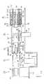
図3は、処理室54(54H,54L)及び処理室載置体100等の構造を示した一部断面側面図である。図3を参照するに、処理室54(54H,54L)は、処理室載置体100の中部において、高さ方向に二段に載置されている。なお、処理室54H及び54Lは、夫々同一の構造を有するため、以下の説明においては、原則として、処理室54Hの説明をもって、処理室54Lの説明に代えることとする。
【0039】
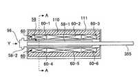
処理室54Hは、例えば、箱型のハウジング56を有する。ハウジング56は、例えば、ステンレス鋼から成る。ハウジング56がゲートバルブ52と当接する接続面400には、半導体基板Wを出し入れするための基板搬入口96が、開口形成されている。ハウジング56の内部には、例えばアルミニウム等から成る筐体111が設けられている。
【0040】
図4は、筐体111の内部の構造を示した側断面図である。図4を参照するに、筐体111の内部には、反応管58、抵抗加熱ヒータ60、断熱材110等が設けられている。
【0041】
反応管58は、筐体111の略中央に水平になるように収容されている。反応管58は、例えば石英、炭化珪素材料(SiC)等の高耐熱性の材質から成る。反応管58は、内部に半導体基板Wが載置される基板載置部58−1と、基板載置部58−1から延在形成され端部において上述の基板搬入口96が開口形成されたフランジ部58−2とから大略構成され、中空の構造を有する。
【0042】
反応管58のフランジ部58−2は、筐体111からはみ出ている。反応管58を筐体111に取り付ける際には、図4において矢印Yで示す方向に基板載置部58−1から筐体111に水平に挿入する。メンテナンス等のために、反応管58を筐体111から取り出すためには、基板搬入口96が開口形成されたフランジ部58−2側から反応管58を引き抜く。
【0043】
図5は、図4に示される反応管58の基板載置部58−1の線A−Aにおける断面を臨む基板載置部58−1等の斜視図である。基板載置部58−1は扁平な中空の直方体形状の薄肉構造を有する。基板載置部58−1の側壁部360には、ガス供給管350が、基板載置部58−1の長手方向(図5におけるX方向)に沿って側壁部360の略中央を貫通するように取り付けられている。同様に、側壁部365には、ガス排気管355が、基板載置部58−1の長手方向(図5におけるX方向)に沿って側壁部365の略中央を貫通するように取り付けられている。
【0044】
ガス供給管350及びガス排気管355は断面が円筒形のパイプ構造を有している。従って、基板載置部58−1の側壁部360、365は、薄肉かつ高さ(図5におけるZ方向の長さ)が短い構造を有するが、上述のガス供給管350及びガス排気管355が取り付けられているため、基板載置部58−1の強度を維持することができる。
【0045】
基板載置部58−1の内部においてガス排気管355に対向しているガス供給管350の側面の上部及び下部には、ガス導入口351が所定の間隔毎にガス供給管350の長手方向(図5におけるX方向)に複数形成されている。同様に、基板載置部58−1の内部においてガス供給管350に対向しているガス排気管355の側面の上部及び下部には、ガス排気口356が所定の間隔毎にガス排気管355の長手方向(図5におけるX方向)に複数形成されている。
【0046】
従って、所定の処理ガスが、ガス供給管350からガス導入口351を介して基板載置部58−1の内部に分散して導入され、また、基板載置部58−1の内部に拡散しているガスは、ガス排気口356を介してガス排気管355へ排気される。
【0047】
ガス供給管350及びガス排気管355の長手方向(図5におけるX方向)の長さは互いに略等しく、基板載置部58−1の長手方向(図5におけるX方向)の長さよりも長い。図3及び図4に示されるように、反応管58のフランジ部58−2が設けられている側と反対の側の、ガス供給管350及びガス排気管355の端部は、筐体111及びハウジング部56よりも外側に位置されている。
【0048】
なお、図2及び図5に示すように、反応管58の内部には、例えば石英等からなる突状支持部98が離散的に複数形成されており、処理対象の半導体ウエアWが略水平に支持される。
【0049】
次に、抵抗加熱ヒータ60について説明する。図6は、図4に示す反応管58及び抵抗加熱ヒータ60との位置関係を示す図であり、図4の線A−Aにおける断面図である。なお、図6では説明の便宜上、断熱材110及び筐体111の図示は省略している。
【0050】
図4及び図6を参照するに、抵抗加熱ヒータ60は、反応管58の上下面及び左右側面に着脱自在に設けられている。
【0051】
具体的には、図4に示すように、抵抗加熱部60のうち、反応管58の上下に向き合って配置される部分においては、反応管58の長手方向において3つのゾーン、即ち、フロントゾーン(60−1,60−4)、ミドルゾーン(60−2,60−5)及びリアゾーン(60−3,60−6)に分割されている。上記3つのゾーンのうち、ミドルゾーン(60−2,60−5)が反応管58の内部に配置される半導体基板Wのほぼ全域をカバーし、フロントゾーン(60−1,60−4)およびリアゾーン(60−3,60−6)が半導体基板Wの前後周辺部をカバーするようにゾーン設定がなされている。
【0052】
また、図6に示すように、反応管58の左右に向き合って配置される部分であるレフトゾーン(60−7)及びライトゾーン(60−8)においても、反応管58の長手方向に沿って抵抗加熱ヒータ60が設けられている。
【0053】
抵抗加熱ヒータ60は、ジュール熱により放射熱を発生して、反応管58内を加熱し均熱雰囲気を形成する。これによって、反応管58内に載置された半導体基板Wが加熱される。抵抗加熱ヒータ60は、セラミックからなる芯棒に二ケイ化モリブデン(MoSi2)等からなる抵抗発熱線や、鉄(Fe)とクロム(Cr)とアルミニウム(Al)の合金線であるカンタル(商品名)線等の抵抗発熱線を一定のピッチまたはリードで巻き付けたコイル状の抵抗発熱素子PEを平面状(二次元方向)に多数配列して形成される。
【0054】
次に、断熱部材110について説明する。図4を再度参照するに、断熱部材110は、筐体111と抵抗加熱ヒータ60との間に、抵抗加熱ヒータ60及び反応管58を囲むように設けられている。断熱部材110は、例えば、セラミック等から成る。
【0055】
上述の内部構造を備えた処理室54(54H,54L)が載置される処理室載置体100の構造を以下において説明する。
【0056】
図3を再度参照するに、処理室載置体100の上部には、処理室54(54H,54L)等を制御するための制御ユニット101が搭載され、処理室載置体100の下部には、処理装置に必要な電源を供給する電源ボックス102等が搭載されている。
【0057】
また、処理室載置体100において、ゲートバルブ52が位置している側と反対側には、処理室56における処理状況等を監視するためのディスプレイ170が設けられている。
【0058】
図7は、図3に示す処理室載置体100及び処理室54(54H,54L)等を、図3において矢印A方向にみたときの図である。
【0059】
図7を参照するに、ハウジング56の背面510からは、上述のように、ガス供給管350及びガス排気管355の端部が延出している。また、反応管58の内部温度を近似値として測定するための温度センサである熱電対112が取り付けられている。
【0060】
また、処理室載置体100の下部には、上述の電源ボックス102のほか、図7において点線で示されるポンプユニット104等が設けられ、処理室54(54H,54L)内を適切に排気するために必要なポンプを備える。
【0061】
上述のディスプレイ170は回動可能に処理室載置体100に取り付けられており、ディスプレイ170を図3に示す状態から約90度回動させた状態が図7に示されている。
【0062】
次に、処理室載置体100の中部における処理室54(54H,54L)の載置構造を説明する。
【0063】
図3を参照するに、処理室載置体100の中部には、処理室支持部材151が図3において左右方向に設けられている。また、処理室54(54H,54L)は、回転機構部300を介して板状部材のベース部材250に載置されている。後述する摺動構造により、処理室54(54H,54L)が載置されているベース部材250は処理室支持部材151を摺動する。
【0064】
また、回転機構部300上に設けられている処理室54(54H,54L)は、回転機構部300により360度回動することができる。
【0065】
図8は、図3に示す処理室54を摺動させ、回転させた状態を示す図である。具体的には、図8において、処理室載置体100の中部に二段に載置されている処理室54のうち、上部に設けられている処理室54Hは、ゲートバルブ52との接続が解除され、図3に示す状態から、図3において矢印Zで示す方向に処理室支持部材151上を摺動された状態にある。また、下部に設けられている処理室54Lは、処理室54Hと同様に、図3に示す状態から図3において矢印Zで示す方向に処理室支持部材151上を摺動させ、更に、90度回動された状態にある。
【0066】
以下、上述の処理室54と処理室54に接続される被接続部材の一例であるゲートバルブ52との接続構造、処理室54の摺動構造、及び回転機構部300の構造について詳述する。
【0067】
先ず、処理室54とゲートバルブ52との接続構造について説明する。
【0068】
図8を参照するに、ゲートバルブ52に接続される処理室54の接続面400の外周のうち、互いに対向する縦の辺、即ち、図8に示す処理室54Lの外周のうち上下方向に形成されている辺の夫々にハンドル部410が2個ずつ設けられている。なお、処理室54Hにおいても、処理室54Lと同様に、ハンドル部410が設けられている。
【0069】
図9は、図8に示すハンドル部410を、図8において矢印B方向からみたときの図である。
【0070】
図8及び図9を参照するに、ハンドル部410は、ハンドルバー411、板状のベース部412、回転軸部413等を含む。ハンドルバー411は、ベース部412を介して接続面400に取り付けられている。回転軸部413は、ベース部412の略中央に備えられている。ハンドルバー411は、回転軸部413によって軸支されており、図8において矢印Cで示す方向にハンドルバー411を90度回動することができる。
【0071】
処理室54の接続面400がゲートバルブ52に当接し、更に、4個のハンドルバー411の全てが横方向(図8において左右方向)に位置するようにハンドルバー411を回動操作すると、Oリング等のシール部材を介して、処理室54の接続面400がゲートバルブ52に加圧密着し、処理室54とゲートバルブ52は完全に接続・接合されてロック状態となる。
【0072】
当該ロック状態を解くためには、ハンドルバー411を90度回動する操作を行い、ハンドルバー411を縦方向、即ち、図8において上下方向に位置させる。
【0073】
このように、処理室54は、クランプ機構として機能するハンドル部410において、ハンドルバー411を回動操作することにより、容易にゲートバルブ52に着脱自在に接続される。
【0074】
次に、処理室54の摺動構造及び回転機構部300の構造について説明する。
【0075】
図10は、図3に示す処理室54Hの摺動構造及び回転機構部300の構造を示すための図であって、図3において矢印Aで示す方向から処理室54H等を見た図である。また、図11は、処理室54Hの摺動構造を示すための図であって、図3において矢印Fで示す方向から処理室54Hを搭載するベース部材250等を見た図である。なお、説明の便宜のため、図11において処理室54の図示は省略している。
【0076】
図10及び図11を参照するに、処理室載置体100の内部に設けられた2本の処理室支持部材151の夫々の略全長に亘って、レール部材150が取り付けられている。
【0077】
図12は、図10において点線Pで示す部分の拡大図である。図12を参照するに、処理室支持部材151の略全長に亘って取り付けられているレール部材150の上部及び下部には、溝が案内レール150−1として形成されている。
【0078】
また、図10及び図11に示されるように、2本のレール部材150の間には、板状部材のベース部材250が設けられている。また、図12を再度参照するに、ベース部材250の外周部分であって、レール部材150に対向する部分には、ベースブロック部材301が螺子止めされている。複数組のローラ200が、ベースブロック部材301の上部及び下部に1個ずつを一組として、案内レール150−1が設けられている方向に沿って回動自在に設けられている。ローラ200は、レール部材150の案内レール150−1を摺動自在に挟持している。
【0079】
かかる構造の下、ベース部材250に取り付けられたローラ200がレール部材150の案内レール150−1を摺動することにより、ベース部材250は、図11において矢印D及びEで示す方向に摺動され、その結果、処理室54Hは、処理室載置体100内を矢印D及びEで示す方向に移動することができる。
【0080】
次に、回転機構部300の構造について説明する。図13は、図10において点線Qで示す部分の拡大図であり、回転機構部300の構造を示す図である。
【0081】
図10及び図13を参照するに、ベース部材250の略中央には、回転機構部300の回転軸部310が設けられている。回転軸部310は、回転軸部310の周りに設けられた軸受部材320によって、360度回動自在に支持されている。回転軸部310及び軸受部材320によって、回転機構部300は大略構成されている。
【0082】
回転軸部310の上面には、処理室54Hが螺子止めされて設けられている。従って、回転軸部310が回動すると、処理室54Hもこれに伴って回動する。即ち、処理室54Hは、回転機構部300により360度回動することができる。
【0083】
図10に示すように、本実施形態では更に、回転機構部300により処理室54Hを90度回動させる度に、その位置で処理室54Hの回動が停止されるように、ベース部材250の上面に設けられたボールプランジャー371及び処理室54Hのハウジング56の下面に形成された凹状孔形成部372から構成される割出し機構部370が設けられている。図14は、図10において点線Rで示す部分の拡大図であり、割出し機構部370の構造が示されている。
【0084】
かかる構造の下、メンテナンス等のために、処理室54Hを以下の如く摺動及び回動することができる。図15は、処理室54Hの摺動及び回動を示す図であり、処理室54Hを上から見た図である。なお、図15中、回転軸部310を点線で示す。
【0085】
図15を参照するに、図15−(a)に示す状態は、図3に示す状態と同じ状態である。即ち、処理室54Hの接続面400はゲートバルブ52に当接し、更に、4個のハンドルバー411の全てが横方向に位置されて処理室54の接続面400はゲートバルブ52に加圧密着し、処理室54Hとゲートバルブ52は完全に接続・接合されてロック状態となっている。
【0086】
図15−(a)に示す状態から、全てのハンドルバー411の方向が上下方向になるようにハンドルバー411を操作してゲートバルブ52との接続を解除し、処理室54Hを図15−(a)において矢印で示す方向に摺動させ、処理室54Hがゲートバルブ52から離間した状態が図15−(b)に示される状態である。この状態では、処理室54Hの接続面400はレール部材150の端部近傍に位置され、ゲートバルブ52と処理室54Hの接続面400との間に隙間が形成されている。
【0087】
図15−(b)に示す状態から、図15−(b)において矢印で示すように処理室54Hを反時計回りに90度回動操作させた状態を図15−(c)に示す。
【0088】
図15−(c)に示す状態は、処理室54Hを搭載するベース部材250(図10参照)を図15−(b)に示す状態に維持したまま、回転軸部310を介して処理室54Hを図15−(b)に示される状態から反時計回りに90度回動し、上述の構造を有する割出し機構部370(図10参照)により、処理室54Hの位置決めがされた状態である。従って、処理室54Hの接続面400は、ゲートバルブ52の開口部分と90度反時計回りに離間した方向にある。
【0089】
なお、図15−(c)では、図15−(b)に示される状態から、処理室54Hを反時計回りに90度回動操作させた状態を示しているが、回転軸部310は360度回動することができるため、処理室54Hを図15−(b)に示される状態から時計回りに90度回動操作することもできる。
【0090】
図15−(c)に示される状態から、図15−(c)において矢印で示すように処理室54Hを反時計回りに更に90度回動操作させた状態、即ち、図15−(b)に示される状態から、処理室54Hを反時計回りに180度回動操作させた状態を図15−(d)に示す。
【0091】
図15−(d)に示される状態は、処理室54Hを搭載するベース部材250(図10参照)を図15−(b)及び図15−(c)に示す状態に維持したまま、回転軸部310を介して処理室54Hを図15−(c)に示す状態から反時計回りに更に90度回動操作し、上述の割出し機構部370(図10参照)により位置決めがされた状態である。従って、処理室54Hの接続面400は、ゲートバルブ52の開口部分と180度離間した方向にある。
【0092】
ところで、上述のように、メンテナンス等のために、図3等に示す反応管58を処理室54Hから抜き出す場合には、図3等に示す基板搬入口96が開口形成されている接続面400から反応管58を引き出す必要がある。
【0093】
本実施形態の構造では、処理室54Hを回動操作することにより、処理室54Hのハウジング56の接続面400を、操作者が操作しやすい位置である処理室載置体100の三方向(ゲートバルブ52の開口部分と90度、180度及び270度離間した方向)の何れの方向にも向けることができ、更に、割出し機構部370により処理室54Hの位置決めをすることができるため、処理室54Hから反応管58を容易に引き出すことができる。
【0094】
即ち、本実施形態の構造では、ハンドル部410を操作してゲートバルブ52との接続が解除された処理室54Hを、処理室54Hを搭載するベース部材250をレール部材150に対して摺動して後方に引き出し、更に、処理室54Hを回転機構部300を介して接続面400が何れの方向にも位置することができるように処理室54を水平方向に回動することができる。これによって、容易に、処理室載置体100のどの方向からも処理室54Hのメンテナンスをすることが可能となる。
【0095】
また、図3に示すように、処理室54Hの上下に、他の構成部材が配置され、上下方向に処理室54Hのメンテナンスのスペースが確保されていない場合でも、処理室54Hが被接続部材であるゲートバルブ52に対し相対的に離間可能に接続され、処理室54Hを回動するための回転機構部300を備え、略同一平面内で離間及び回動可能に構成されているため、処理室54Hのメンテナンスを行うことができる。
【0096】
次に、図7に示すハウジング56の背面510、即ち、ハウジング56の接続面400と反対の側の面に取り付けられている熱電対112や、図3に示すハウジング56の内部に設けられている抵抗加熱ヒータ60等のメンテナンスをする場合について説明する。
【0097】
図16は、図7に示す熱電対112や図3に示す抵抗加熱ヒータ60のメンテナンス等をするための、処理室54Hの移動及び操作を説明するための処理室54H等の側面模式図であり、(a)は本発明を利用した場合を示し、(b)は従来技術を利用した場合を示している。
【0098】
本発明を利用した場合は、図16−(a)に示されるように、ゲートバルブ52との接続が解除された処理室54Hを、処理室54Hの背面側510に設けられた蓋体500が処理室載置体100の外部にはみ出る位置まで矢印Kで示す方向に引き出して移動させる。処理室54の移動の停止後、蓋体500を矢印Gで示す方向に回動操作し、蓋体500を開ける。なお、前述のように、図3に示すディスプレイ170は図7に示すように回動操作することができ、蓋体500の開閉の妨害とはならない。蓋体500を開けることにより、容易に、図3に示す抵抗加熱ヒータ60を取り出したり、背面510に設けられている図7に示す熱電対112を取り外すことができる。
【0099】
これに対し、従来の技術を利用した場合は、図16−(b)に示されるように処理室700を、処理室700の全てが処理室載置体710からはみ出る位置まで矢印Mで示す方向に引き出して移動させる。処理室700の移動の停止後、処理室700の上部に設けられている板状の蓋部715を矢印Nで示す方向に、即ち、上側に回動させる必要がある。
【0100】
即ち、従来であれば、処理室700の全てを処理室載置体710から引き出し、更に、処理室700の上部に設けられている蓋部715を開けなければならなかったが、本実施形態では、処理室54Hを処理室載置体100から全部引き出さずに、蓋体500が処理室載置体100の外部にはみ出る分だけ引き出せば足り、重量のある処理室54Hを安定して操作することができる。
【0101】
以上のような本発明の構造によれば、処理モジュール18の近傍に装置が設けられていても、処理室54Hのメンテナンスのために処理モジュール18にアクセスするに必要な領域は僅かで足りる。従って、処理装置の総設置面積(フットプリント)を拡充することなく処理室54のメンテナンスを行うことができる。また、処理室54のゲートバルブ52からの引き出し量を低減でき、更に、反応管58や抵抗加熱ヒータ60や熱電対112等のメンテナンスをどの方向からも容易に行うことができる。即ち、アクセスし易い方向でのメンテナンスが可能となるとともに、フットプリントを小さくすることが可能となる。
【0102】
次に、上述のような構成を有する処理装置における基板の搬送及び処理について説明する。
【0103】
図1及び図2を再度参照するに、ローダ/アンローダ部12の基板搬送機構22は、カセットステーション10より未処理の半導体基板Wをほぼ水平に1枚取り出すと、搬送アーム26を旋回させ、アライメントユニット38に搬入する。
【0104】
基板搬送機構22は、アライメントユニット38において位置合わせを終えた半導体基板Wをアライメントユニット38から搬出し、ロードロック室28の前まで移動する。半導体基板Wがロードロック室28に収容配置されると、トランスファ・モジュール16の搬送室40内で搬送アーム42が移動動作し、半導体基板Wを取り出す。搬送アーム42は所定角度旋回して、プロセス・モジュール18の処理室54に半導体基板Wを配置する。処理室54において、未処理の半導体基板Wは高温の急速熱処理を受ける。
【0105】
トランスファ・モジュール16において、搬送アーム42は、高温の急速熱処理を施された半導体基板Wを搬出すると、所定角度旋回して、当該半導体基板Wを冷却処理室30へ配置する。
【0106】
処理室54において急速熱処理を受けた半導体基板Wは、冷却処理室30において以下の如く冷却される。
【0107】
図17乃至図19は、冷却処理室30における半導体基板Wの冷却処理を説明するための模式図である。
【0108】
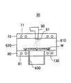
図17乃至図19を参照するに、冷却処理室30は、搬送アーム42(図1参照)によって搬送された半導体基板Wを密閉雰囲気下に置くべく、密閉されている。冷却処理室30の上部には上部冷却板70が、下部には下部冷却板80が、互いに対向して設けられている。上部冷却板70及び下部冷却板80は、例えば熱伝導性の高いアルミ合金から成り、水冷式冷却機構を採用している。即ち、上部冷却板70の内部には複数の上部冷却水管路71が、また、下部冷却板80の内部には複数の下部冷却水管路81が埋設されている。
【0109】
図示を省略する冷却装置によって、半導体基板Wの冷却設定温度に冷却された冷却水を、例えばステンレス製のパイプから成る上部冷却水管路71及び下部冷却水管路81の内部を熱交換させながら流通させて、上部冷却板70及び下部冷却板80を冷却している。
【0110】
上部冷却板70及び下部冷却板80には、図示を省略する温度センサ等が取り付けられており,冷却板が所望の温度に保たれるよう制御される。従って、後述するように、冷却処理室30に搬入された半導体基板Wを、上部冷却板70及び下部冷却板80の冷熱によって冷却処理することができる。
【0111】
なお、上述の如く、本実施形態では、水冷式冷却機構が上部冷却板70及び下部冷却板80に採用されているが、空冷式冷却機構を採用してもよく、また、上部冷却板70及び下部冷却板80に、冷却素子であるペルチェ素子を冷却素子として複数内蔵する冷却手段を備えた構造としてもよい。
【0112】
上部冷却板70の略中央内を連通するように、冷却媒体供給管90が設けられている。冷却媒体供給管90を介して、窒素、ヘリウム等の不活性ガスが冷却媒体として冷却処理室30内に供給される。冷却媒体供給管90の先端にはガス拡散ノズル91が設けられ、上記ガスの分散角度や流速が調整される。
【0113】
下部冷却板80であって、上部冷却板70と対向する面上には、半導体基板Wを、下部冷却板80の上部冷却板70と対向する面から約0.1mm乃至2mm、望ましくは約0.3mm浮かせた状態で半導体基板Wを支持する支持突起部130が、複数(例えば、3個)突出して設けられている。支持突起部130は、例えば樹脂等からなる。
【0114】
また、下部冷却板80には、複数(例えば、3個)の昇降ピン貫通穴形成部82が、その内部において昇降ピン630が昇降自在に挿入できるように、鉛直方向に貫通して設けられている。
【0115】
昇降ピン630は、半導体基板Wを支持し昇降させる昇降手段として機能する。昇降ピン630は、図示を省略する昇降駆動手段により昇降する。例えば、下部冷却板80の下部に、機械室を設け、この機械室内に、モータ、昇降ピンアーム及び昇降ピンアーム駆動用シリンダ等の駆動機構が取り付けられ、これらによって昇降ピン630を所定のタイミングで上下動するように駆動される。昇降ピン630は、昇降ピン貫通穴形成部82の内部を上方向に移動して、下部冷却板80の上方に突出できるようになっている。
【0116】
上述のように、冷却処理室30の側面には、基板搬入口610が開口して設けられている。基板搬入口610は、図1に示すトランスファ・モジュール16に、図1に示すゲートバルブ36を介して連結されている。従って、基板搬入口610は、半導体基板Wが、図1に示すトランスファ・モジュール16の搬送室40内に設けられた搬送アーム42によって冷却処理室30に搬入される入口として機能する。
【0117】
また、基板搬入口610が設けられている側面に対向する冷却処理室30の側面には、基板搬出口620が開口して設けられている。基板搬出口620は、冷却処理室30内で以下に説明する冷却処理によって冷却された半導体基板Wを、図1に示すローダ/アンローダ部12の図1に示す基板搬送機構22によって、冷却処理室30の外部へ搬出するための出口として機能する。
【0118】
上述のような構造を有し、密閉された冷却処理室30において、以下の如く、半導体基板は冷却処理される。本実施形態においては、冷却処理工程中、半導体基板Wは後述する3種類の位置(第1乃至第3の位置)に停止される。
【0119】
図17は、図1等に示す処理室56内で、高温の急速熱処理により高温状態となった半導体基板Wが、基板搬入口610を介して搬送アーム42によって冷却処理室30内に搬入され、搬入された際の高さ位置(第1の位置)で搬送アーム42の動作が停止された状態を示している。
【0120】
半導体基板Wが、搬送アーム42によって冷却処理室30内に搬入されると直ちに、上部冷却板70の略中央内を連通するように設けられ半導体基板Wの上面側に位置づけられた冷却媒体供給管90の先端に設けられたガス拡散ノズル91から、窒素、ヘリウム等の不活性ガスが冷却媒体として供給され、半導体基板Wが冷却される。これ以降、半導体基板Wの冷却処理が完了するまで、冷却媒体は冷却処理室30内に絶えず供給され続ける。
【0121】
従って、冷却処理室30に搬入された半導体基板Wは、冷却処理室30に搬入されると直ちに、上部冷却板70及び下部冷却板80の冷熱と、半導体基板Wの上部から供給される冷却媒体とによって、半導体基板Wの上側と下側の双方から冷却される。
【0122】
よって、半導体基板Wは、処理室54で急速熱処理が施された面の略中央部と周縁部における温度差に起因して山形に反ってしまう等の変形(熱ひずみ)が発生することはなく、平面において真っ直ぐな状態が維持される。
【0123】
また、かかる状態においては、昇降ピン630が、図示を省略する昇降駆動手段によって駆動され、下部冷却板80に鉛直方向に貫通形成された複数(例えば、3個)の昇降ピン貫通穴形成部82を介して下部冷却板80の上方向に移動し下部冷却板80の上面から突出している。
【0124】
半導体基板Wは、図17に示す第1の位置から所定の時間経過後、以下の工程を経て、図18に示す第2の位置に置かれる。
【0125】
即ち、先ず、半導体基板Wを冷却処理室30内に搬入した搬送アーム42が、半導体基板Wを昇降ピン630上に受け渡す。具体的には、半導体基板Wを支持している搬送アーム42が図17において矢印Sで示す方向に下降され、半導体基板Wは、昇降ピン630上(第2の位置)に載置される。次いで、搬送アーム42は、図18において矢印Tで示す方向に引き抜かれ、冷却処理室30から退避される。
【0126】
上述のように、半導体基板Wは、冷却処理室30内に搬入されると、半導体基板Wの前記面の略中央部と周縁部における温度差に起因する半導体基板Wの変形(熱ひずみ)は発生せず、真っ直ぐな平面状態が維持されている。従って、かかる真っ直ぐな平面状態が維持されたまま、半導体基板Wは昇降ピン630上に載置される。
【0127】
この後、半導体基板Wは、図18に示す第2の位置から、以下の工程を経て、図19に示す第3の位置に置かれる。
【0128】
即ち、先ず、半導体基板Wが載置された昇降ピン630は、図示を省略する昇降駆動手段によって駆動され、下部冷却板80に鉛直方向に貫通形成された複数(例えば、3個)の昇降ピン貫通穴形成部82を介して、半導体基板Wが支持突起部130上(第3の位置)に当接するまで、図18中矢印Uで示す方向に下降される。
【0129】
上述のように、支持突起部130は、下部冷却板80の上面から僅かに突出するように設けられているので、半導体基板Wは、下部冷却板80に近接した状態で支持突起部130に支持される。かかる状態で、半導体基板Wは、下部冷却板80により、冷却処理室30内で所望の温度、例えば、常温まで冷却される。
【0130】
ここで、上述のように、半導体基板Wは、真っ直ぐな平面状態が維持されたまま昇降ピン630上に載置され、その後、支持突起部130に載置されるため、半導体基板Wは、真っ直ぐな平面状態が維持されたまま冷却処理室30の下側から冷却される。
【0131】
冷却処理室30の中で所定温度まで半導体基板Wを冷却する冷却処理が完了すると、冷却媒体供給管90から冷却処理室30への冷却媒体の供給は停止される。
【0132】
半導体基板Wの冷却処理が完了すると、図1に示すローダ/アンローダ部12の基板搬送機構22が冷却処理室30に基板搬出口120からアクセスし、半導体基板Wは、冷却処理室30から搬出される。
【0133】
このように、半導体基板Wが冷却処理室30内に搬入された時点から冷却処理が完了するまで、冷却処理室30の上側に設けられた冷却媒体供給管90から冷却処理室30へ冷却媒体が供給され続け、半導体基板Wは上側からも冷却処理されている。
【0134】
従って、冷却処理室30の下側に設けられた下側冷却板80に設けられた支持突起部130に半導体基板Wを載置して冷却処理室30の中で所定温度まで半導体基板Wを冷却処理する前に、半導体基板Wの前記面の略中央部と周縁部における温度差に起因する半導体基板Wの変形(熱ひずみ)が発生することが回避され、真っ直ぐな平面状態を維持したまま半導体基板Wに冷却処理を施すことができる。その結果、所望の短時間内に、半導体基板W全体を均一に冷却することができる。
【0135】
このように、冷却処理に要する時間を短縮することができ、更に、確実に半導体基板Wを冷却することができるため、スループットの向上を図ることが出来る。
【0136】
図1及び図2を再度参照するに、基板搬送機構22は、冷却処理室30より半導体基板Wを取り出すと、搬送アーム26を旋回させ、カセットステーション10の所望のカセットCRの前に移動し、カセットCRに処理済の半導体基板Wを挿し込まれる。
【0137】
以上本発明の好ましい実施形態について詳述したが、本発明は係る特定の実施形態に限定されるものではなく、特許請求の範囲に記載された本発明の要旨の範囲内において、種々の変形・変更が可能である。
【0138】
例えば、上述の実施形態では、回転軸部310及び軸受部材320によって、回転機構部300が構成されているが、本発明はこれに限られず、処理室を回動することができれば如何なる構造であってもよい。
【0139】
また、上述の実施形態では、ベース部材250の摺動にあっては、ローラ200及びレール部材250が用いられているが、本発明はこれに限られず、処理室54をゲートバルブ52から離間することができれば、如何なる構造であってもよい。
【0140】
更に、上述の実施形態では、レール部材150を摺動するベース部材150の上に回転機構部300が設けられ当該回転機構部300の上に処理室54が設けられている構造を示したが、本発明はこれに限られず、回転機構部の上に摺動自在のベース部材が備えられ、その上に処理室が設けられても良い。或いは、処理室を上方からぶら下げる構造にし、処理室の上に回転機構部及び摺動機構部を設けられていてもよい。
【0141】
また、上述の実施形態では、割出し機構部370は互いに90度離間した位置に4つ設けられているが、処理室54を回動して位置決めができる限り、本発明はこれに限られない。
【0142】
【発明の効果】
以上詳述したところから明らかなように、本発明の処理装置によれば、メンテナンスのために必要とされるスペースを極力小さくし、簡易なメンテナンス操作の実現を可能とし、処理室のメンテナンス性の向上を図ることができる。
【図面の簡単な説明】
【図1】本発明の一実施形態における処理装置の全体構成を模式的に示す一部断面側面図である。
【図2】本発明の一実施形態における処理装置の全体構成を模式的に示す平面図である。
【図3】処理室54(54H,54L)及び処理室載置体100等の構造を示した一部断面側面図である。
【図4】筐体111の内部の構造を示した側断面図である。
【図5】図4に示される反応管58の基板載置部58−1の線A−Aにおける断面を臨む基板載置部58−1等の斜視図である。
【図6】図4に示す反応管58及び抵抗加熱ヒータ60との位置関係を示す図であり、図4の線A−Aにおける断面図である。
【図7】図3に示す処理室載置体100及び処理室54(54H,54L)等を図3において矢印A方向にみたときの図である。
【図8】図3に示す処理室54を摺動させ、回転させた状態を示す図である。
【図9】図8に示すハンドル部410を図8において矢印B方向からみたときの図である。
【図10】図3に示す処理室54Hの摺動構造及び回転機構部300の構造を示すための図であって、図3において矢印Aで示す方向から処理室54H等を見た図である。
【図11】処理室54Hの摺動構造を示すための図であって、図3において矢印Fで示す方向から処理室54Hを搭載するベース部材250等を見た図である。
【図12】図10において点線Hで示す部分の拡大図である。
【図13】図10において点線Qで示す部分の拡大図である。
【図14】図10において点線Rで示す部分の拡大図である。
【図15】処理室54Hの摺動及び回動を示す図であり、処理室54Hを上から見た図である。
【図16】図7に示す熱電対112や図3に示す抵抗加熱ヒータ60のメンテナンス等をするための、処理室54Hの移動及び操作を説明するための処理室54H等の側面模式図である。
【図17】冷却処理室30における半導体基板Wの冷却処理を説明するための模式図である。
【図18】冷却処理室30における半導体基板Wの冷却処理を説明するための模式図である。
【図19】冷却処理室30における半導体基板Wの冷却処理を説明するための模式図である。
【符号の説明】
10 カセットステーション
12 ローダ/アンローダ部
18 処理モジュール
28(28H、28L) ロードロック室
30(30H、30L) 冷却処理室
40 搬送室
42 搬送アーム
52 ゲートバルブ
54(54H、54L) 処理室
56 ハウジング
58 反応管
60 抵抗加熱ヒータ
300 回転機構部
310 回転軸部
370 割出し機構部
410 ハンドル部
411 ハンドルバー[0001]
TECHNICAL FIELD OF THE INVENTION
The present invention relates to a processing apparatus used in a manufacturing process such as a semiconductor device, an LCD (Liquid Crystal Display) or an FPD (Flat Panel Display), and a method of moving a processing chamber provided in the processing apparatus. The present invention relates to a processing apparatus for performing predetermined processing on a substrate to be processed (semiconductor substrate, LCD substrate, FPD substrate, or the like) using a predetermined processing gas in a processing chamber, and a method of moving the processing chamber.
[0002]
[Prior art]
2. Description of the Related Art In a processing apparatus used in a manufacturing process such as a semiconductor device, an LCD (Liquid Crystal Display) or an FPD (Flat Panel Display), a vacuum chamber such as a load lock chamber or an inert gas atmosphere chamber is provided before and / or after a processing chamber. ing. Thus, the substrate to be processed is carried into or out of the processing chamber without opening the processing chamber to the atmosphere. In particular, in the multi-chamber system, a plurality of processing chambers are arranged around a transfer chamber that can be sealed, and a substrate to be processed is arbitrarily loaded / unloaded into each processing chamber through the transfer chamber. reference).
[0003]
In general, in the multi-chamber system, one of a plurality of chambers is used as a cooling chamber, a processed substrate is cooled to a predetermined temperature in the cooling chamber, and then a load (or a cassette) is accommodated or disposed therein. It is transported through the transport chamber to the lock chamber or cassette station.
[0004]
By the way, in the processing chamber provided in the processing apparatus, the film quality is deteriorated as the film formation is continued, and the film is formed also in the reaction tube provided inside the processing chamber, and the inside of the reaction tube needs to be cleaned. . Further, maintenance is required when a failure occurs in a heating source such as a thermocouple or a heater attached to the processing chamber. Therefore, conventionally, a lid that can be opened and closed is provided at the upper part of the processing chamber, and the lid is opened to perform a maintenance operation inside the processing chamber.
[0005]
However, in order to simultaneously perform single-wafer processing on a plurality of substrates, a plurality of processing chambers are arranged in multiple stages in the height direction of the processing apparatus, and a plurality of substrates to be processed are simultaneously or in parallel in the processing chambers. In the case of a processing apparatus that adopts a structure in which the processing chamber is taken in and out, it is not possible to perform a maintenance operation from above the processing apparatus by opening a lid provided at an upper portion of the processing chamber.
[0006]
For this reason, in a processing apparatus in which the processing chambers are arranged in multiple stages in the height direction of the processing apparatus, conventionally, a method of pulling out the processing chamber and performing maintenance of the processing chamber has been adopted.
[0007]
For example, in a structure in which a plurality of chamber units are detachably attached to a plurality of mounting sections formed on a base frame, the chamber units are slid with respect to the mounting section to perform maintenance on the chamber units. A structure that can be attached and detached and detached from a base frame is adopted (for example, see Patent Document 2).
[0008]
Further, there is also a structure in which a processing chamber is detachably connected to a transfer chamber in a state where the transfer chamber is closed, and the processing chamber is movably mounted on a guide rail via wheels (for example, Patent Reference 3).
[0009]
With such a structure, even when the processing chambers are arranged in multiple stages in the height direction of the processing apparatus, the processing chamber is provided at the upper part of the processing chamber by performing an operation of pulling out the processing chamber connected to the transfer chamber. By opening the lid, a space for performing a maintenance operation from above the processing apparatus can be secured.
[0010]
[Patent Document 1]
JP-A-8-111449 (page 2, FIG. 1)
[0011]
[Patent Document 2]
JP-A-8-32470 (pages 1-3, FIG. 1)
[0012]
[Patent Document 3]
JP-A-4-254350 (pages 1-3, FIG. 1)
[0013]
[Problems to be solved by the invention]
However, in any of the above-described structures, it is necessary to pull out the processing chamber from the transfer chamber to which the processing chamber is connected. Therefore, a sufficiently large installation area of the processing apparatus is required to perform the drawing operation.
[0014]
In particular, when a processing apparatus is installed adjacent to another apparatus in a place where the total installation area (footprint) of the processing apparatus is limited, such as in a factory, a space for maintenance of the processing apparatus is limited. You. Therefore, it is difficult to perform maintenance of the processing chamber within the limited space with the conventional structure that needs to secure a sufficient space for the drawing operation.
[0015]
In addition, since the weight of the processing chamber is large, if the processing chamber is simply pulled out from the transfer chamber by sliding or the like as in the conventional structure, the operation of attaching / detaching the processing chamber to / from the transfer chamber requires heavy labor, which is difficult to perform. Having.
[0016]
Accordingly, an object of the present invention has been made in view of the above-described problem, and minimizes the space required for maintenance, enables a simple maintenance operation, and improves the maintainability of the processing chamber. The object of the present invention is to provide a processing device aiming at the above.
[0017]
[Means for Solving the Problems]
An object of the present invention is to provide a processing apparatus including a processing chamber and a connected member connected to the processing chamber, wherein the processing chamber is connected to the connected member so as to be relatively separated from each other, and rotates the processing chamber. This is achieved by a processing apparatus further comprising a rotating mechanism for moving, and configured to be separated and rotatable in substantially the same plane.
[0018]
The above object is also provided in multiple stages, including a substrate accommodating portion for accommodating a plurality of substrates to be processed, and a plurality of processing chambers for performing a predetermined process on the substrate to be processed using a predetermined processing gas in a sealable room. Processed part, between the substrate storage part and the processing part, an unprocessed substrate placement part for temporarily retaining an unprocessed substrate among the processed substrates, the substrate storage part, A processed substrate placement unit that temporarily holds a processed substrate among the processed substrates, a processing unit, the substrate storage unit and the unprocessed substrate placement unit or the processed substrate placement unit. A first transfer unit for transferring the substrate to be processed between the processing unit and the unprocessed substrate placement unit or the processed substrate placement unit; A second transfer means, a transfer chamber having the second transfer means therein, In the processing apparatus, which is connected to the processing chamber and has a connected member that connects the transfer chamber and the processing chamber, the processing chamber is connected to the connected member so as to be relatively separated from each other, The present invention is attained by a processing apparatus characterized by further comprising a rotation mechanism for rotating the processing chamber.
[0019]
BEST MODE FOR CARRYING OUT THE INVENTION
Hereinafter, embodiments of the present invention will be described with reference to the drawings. In the drawings, the same components are denoted by the same reference numerals.
[0020]
First, the overall configuration of the processing apparatus according to the present invention will be described.
[0021]
FIG. 1 is a partial cross-sectional side view schematically illustrating the entire configuration of a processing apparatus according to an embodiment of the present invention, and FIG. 2 is a schematic view illustrating the entire configuration of the processing apparatus according to an embodiment of the present invention. It is a top view. This processing apparatus performs heat treatment such as oxidation, diffusion, annealing, and thermal CVD (Chemical Vapor Deposition) by a rapid heating method in a manufacturing process of a semiconductor device, an LCD (Liquid Crystal Display), or an FPD (Flat Panel Display). Device.
[0022]
Referring to FIGS. 1 and 2, the processing apparatus includes a
[0023]
In the
[0024]
For example, an unmanned transport vehicle (not shown) accesses the
[0025]
The loader /
[0026]
The
[0027]
The
[0028]
The pair of
[0029]
A plurality of, for example, three
[0030]
In the
[0031]
In the
[0032]
Adjacent to the
[0033]
The
[0034]
Under such a structure, the
[0035]
Openings for connecting the
[0036]
The
[0037]
The
[0038]
FIG. 3 is a partial cross-sectional side view showing the structure of the processing chamber 54 (54H, 54L), the processing
[0039]
The
[0040]
FIG. 4 is a side sectional view showing the internal structure of the
[0041]
The
[0042]
The flange 58-2 of the
[0043]
FIG. 5 is a perspective view of the substrate mounting part 58-1 and the like, which is a cross-sectional view of the substrate mounting part 58-1 of the
[0044]
The
[0045]
In the upper and lower sides of the
[0046]
Therefore, a predetermined processing gas is dispersed and introduced from the
[0047]
The lengths of the
[0048]
As shown in FIGS. 2 and 5, a plurality of projecting
[0049]
Next, the
[0050]
Referring to FIGS. 4 and 6, the
[0051]
Specifically, as shown in FIG. 4, in a portion of the
[0052]
As shown in FIG. 6, the left zone (60-7) and the right zone (60-8), which are the parts arranged to face left and right of the
[0053]
The
[0054]
Next, the
[0055]
The structure of the processing
[0056]
Referring again to FIG. 3, a
[0057]
Further, a
[0058]
FIG. 7 is a diagram when the processing
[0059]
Referring to FIG. 7, the ends of the
[0060]
In addition to the
[0061]
The above-described
[0062]
Next, the mounting structure of the processing chamber 54 (54H, 54L) in the center of the processing
[0063]
Referring to FIG. 3, a processing
[0064]
In addition, the processing chamber 54 (54 </ b> H, 54 </ b> L) provided on the
[0065]
FIG. 8 is a diagram showing a state where the
[0066]
Hereinafter, a connection structure between the
[0067]
First, a connection structure between the
[0068]
Referring to FIG. 8, the outer periphery of the
[0069]
FIG. 9 is a diagram when the
[0070]
8 and 9, the
[0071]
When the
[0072]
In order to release the locked state, an operation of rotating the
[0073]
As described above, the
[0074]
Next, the sliding structure of the
[0075]
FIG. 10 is a view showing the sliding structure of the
[0076]
Referring to FIGS. 10 and 11, a
[0077]
FIG. 12 is an enlarged view of a portion indicated by a dotted line P in FIG. Referring to FIG. 12, grooves are formed as guide rails 150-1 at upper and lower portions of a
[0078]
As shown in FIGS. 10 and 11, a plate-
[0079]
Under such a structure, when the
[0080]
Next, the structure of the
[0081]
Referring to FIGS. 10 and 13, the
[0082]
A
[0083]
As shown in FIG. 10, in the present embodiment, each time the
[0084]
Under such a structure, the
[0085]
Referring to FIG. 15, the state shown in FIG. 15- (a) is the same as the state shown in FIG. That is, the
[0086]
From the state shown in FIG. 15- (a), the
[0087]
FIG. 15- (c) shows a state in which the
[0088]
The state shown in FIG. 15- (c) is such that the base member 250 (see FIG. 10) on which the
[0089]
Note that FIG. 15- (c) shows a state in which the
[0090]
From the state shown in FIG. 15- (c), the
[0091]
The state shown in FIG. 15- (d) is obtained by maintaining the base member 250 (see FIG. 10) for mounting the
[0092]
By the way, as described above, when the
[0093]
In the structure of the present embodiment, by rotating the
[0094]
That is, in the structure of the present embodiment, the
[0095]
Further, as shown in FIG. 3, even when other components are arranged above and below the
[0096]
Next, the
[0097]
FIG. 16 is a schematic side view of the
[0098]
When the present invention is used, as shown in FIG. 16A, the
[0099]
On the other hand, when the conventional technology is used, as shown in FIG. 16B, the
[0100]
That is, in the related art, the
[0101]
According to the structure of the present invention as described above, even if an apparatus is provided in the vicinity of the
[0102]
Next, transport and processing of a substrate in the processing apparatus having the above-described configuration will be described.
[0103]
Referring to FIGS. 1 and 2 again, when one unprocessed semiconductor substrate W is taken out from the
[0104]
The
[0105]
In the
[0106]
The semiconductor substrate W that has been subjected to the rapid thermal processing in the
[0107]
FIGS. 17 to 19 are schematic diagrams for explaining the cooling process of the semiconductor substrate W in the cooling
[0108]
17 to 19, the cooling
[0109]
The cooling water cooled to the cooling set temperature of the semiconductor substrate W is circulated by a cooling device (not shown) while exchanging heat inside the upper
[0110]
A temperature sensor or the like (not shown) is attached to the
[0111]
As described above, in the present embodiment, the water-cooling type cooling mechanism is employed for the
[0112]
A cooling
[0113]
On the
[0114]
Further, a plurality of (for example, three) elevating pin through-
[0115]
The elevating pins 630 function as elevating means for supporting and elevating the semiconductor substrate W. The lifting pins 630 are raised and lowered by lifting driving means (not shown). For example, a machine room is provided below the
[0116]
As described above, the side of the cooling
[0117]
Further, on the side surface of the cooling
[0118]
The semiconductor substrate is cooled in the hermetically sealed
[0119]
FIG. 17 shows a state in which the semiconductor substrate W brought into a high-temperature state by the high-temperature rapid heat treatment in the
[0120]
As soon as the semiconductor substrate W is carried into the cooling
[0121]
Accordingly, as soon as the semiconductor substrate W carried into the cooling
[0122]
Therefore, the semiconductor substrate W does not undergo deformation (thermal strain) such as warping into a mountain shape due to a temperature difference between the substantially central portion and the peripheral portion of the surface subjected to the rapid heat treatment in the
[0123]
In this state, the lifting pins 630 are driven by lifting driving means (not shown), and a plurality of (for example, three) lifting pin through-
[0124]
After a predetermined time has elapsed from the first position shown in FIG. 17, the semiconductor substrate W is placed at the second position shown in FIG. 18 through the following steps.
[0125]
That is, first, the
[0126]
As described above, when the semiconductor substrate W is carried into the cooling
[0127]
Thereafter, the semiconductor substrate W is placed at the third position shown in FIG. 19 from the second position shown in FIG. 18 through the following steps.
[0128]
That is, first, the lifting pins 630 on which the semiconductor substrate W is mounted are driven by lifting driving means (not shown), and a plurality of (for example, three) lifting pins formed through the
[0129]
As described above, since the
[0130]
Here, as described above, the semiconductor substrate W is placed on the elevating
[0131]
When the cooling processing for cooling the semiconductor substrate W to a predetermined temperature in the cooling
[0132]
When the cooling processing of the semiconductor substrate W is completed, the
[0133]
As described above, the cooling medium is supplied from the cooling
[0134]
Therefore, the semiconductor substrate W is placed on the
[0135]
As described above, the time required for the cooling process can be shortened, and the semiconductor substrate W can be surely cooled, so that the throughput can be improved.
[0136]
Referring again to FIGS. 1 and 2, when the semiconductor substrate W is taken out from the cooling
[0137]
Although the preferred embodiment of the present invention has been described in detail above, the present invention is not limited to the specific embodiment, and various modifications and changes may be made within the scope of the present invention described in the appended claims. Changes are possible.
[0138]
For example, in the above-described embodiment, the
[0139]
In the above-described embodiment, the
[0140]
Further, in the above-described embodiment, the structure in which the
[0141]
Further, in the above-described embodiment, four
[0142]
【The invention's effect】
As is apparent from the details described above, according to the processing apparatus of the present invention, the space required for maintenance is reduced as much as possible, a simple maintenance operation can be realized, and the maintenance performance of the processing chamber is improved. Improvement can be achieved.
[Brief description of the drawings]
FIG. 1 is a partial cross-sectional side view schematically illustrating an entire configuration of a processing apparatus according to an embodiment of the present invention.
FIG. 2 is a plan view schematically showing the entire configuration of the processing apparatus according to the embodiment of the present invention.
FIG. 3 is a partial cross-sectional side view showing a structure of a processing chamber 54 (54H, 54L), a processing
FIG. 4 is a side sectional view showing an internal structure of a
FIG. 5 is a perspective view of the substrate mounting portion 58-1 and the like facing a section taken along line AA of the substrate mounting portion 58-1 of the
6 is a diagram showing a positional relationship between a
7 is a diagram of the processing
8 is a view showing a state where the
9 is a view of the
10 is a view showing the sliding structure of the
11 is a view showing a sliding structure of the
FIG. 12 is an enlarged view of a portion indicated by a dotted line H in FIG.
FIG. 13 is an enlarged view of a portion indicated by a dotted line Q in FIG.
FIG. 14 is an enlarged view of a portion indicated by a dotted line R in FIG.
FIG. 15 is a diagram illustrating sliding and rotation of the
16 is a schematic side view of the
FIG. 17 is a schematic diagram for explaining a cooling process of the semiconductor substrate W in the cooling
FIG. 18 is a schematic diagram for explaining a cooling process of the semiconductor substrate W in the cooling
FIG. 19 is a schematic diagram for explaining a cooling process of the semiconductor substrate W in the cooling
[Explanation of symbols]
10 cassette station
12 Loader / Unloader section
18 Processing module
28 (28H, 28L) Load lock chamber
30 (30H, 30L) cooling processing chamber
40 transfer room
42 Transfer arm
52 Gate valve
54 (54H, 54L) processing room
56 Housing
58 Reaction tube
60 resistance heater
300 Rotation mechanism
310 Rotating shaft
370 Indexing mechanism
410 Handle
411 Handlebar
Claims (7)
Translated fromJapanese前記処理室は、前記被接続部材に対し相対的に離間可能に接続され、
前記処理室を回動するための回転機構部を更に備え、
略同一平面内で離間及び回動可能に構成されたことを特徴とする処理装置。In a processing apparatus including a processing chamber and a connected member connected to the processing chamber,
The processing chamber is connected to the connected member so as to be relatively separable,
A rotation mechanism for rotating the processing chamber,
A processing apparatus characterized in that the processing apparatus is configured to be able to separate and rotate in substantially the same plane.
前記処理室は、前記回転軸部の上部に設けられ、前記回転軸部の回動に伴って回動されることを特徴とする請求項1記載の処理装置。The rotation mechanism section includes a rotation shaft section,
2. The processing apparatus according to claim 1, wherein the processing chamber is provided above the rotation shaft, and is rotated with rotation of the rotation shaft. 3.
前記ハンドル部を回動操作することによって、前記処理室は前記被接続部材に接続又は接続が解除されることを特徴とする請求項1乃至3いずれか一項記載の処理装置。The processing chamber includes a handle portion that is clamped to the connected member,
4. The processing apparatus according to claim 1, wherein the processing chamber is connected to or disconnected from the connected member by rotating the handle. 5.
密閉可能な室内で前記被処理基板に所定の処理ガスを用いて所定の処理を施すための複数の処理室が多段に設けられた処理部と、
前記基板収容部と前記処理部との間で、前記被処理基板のうち未処理の被処理基板を一時的に留め置く未処理基板配置部と、
前記基板収容部と前記処理部との間で、前記被処理基板のうち処理済の被処理基板を一時的に留め置く処理済基板配置部と、
前記基板収容部と前記未処理基板配置部又は前記処理済基板配置部との間で前記被処理基板を搬送するための第1の搬送手段と、
前記処理部と前記未処理基板配置部又は前記処理済基板配置部との間で前記被処理基板を搬送するための第2の搬送手段と、
前記第2の搬送手段を内部に備えた搬送室と、
前記処理室に接続され、前記搬送室と前記処理室とを連結する被接続部材と、を備えた処理装置において、
前記処理室は、前記被接続部材に対し相対的に離間可能に接続され、
前記処理室を回動するための回転機構部を更に備えたことを特徴とする処理装置。A substrate storage unit that stores a plurality of substrates to be processed,
A processing unit in which a plurality of processing chambers for performing predetermined processing using a predetermined processing gas on the substrate to be processed in a sealable chamber are provided in multiple stages;
Between the substrate storage unit and the processing unit, an unprocessed substrate placement unit that temporarily holds an unprocessed substrate among the processed substrates,
Between the substrate storage unit and the processing unit, a processed substrate placement unit that temporarily holds a processed substrate to be processed among the substrates to be processed,
A first transport unit for transporting the substrate to be processed between the substrate storage unit and the unprocessed substrate placement unit or the processed substrate placement unit;
A second transport unit for transporting the substrate to be processed between the processing unit and the unprocessed substrate placement unit or the processed substrate placement unit,
A transfer chamber having the second transfer means therein;
A connected member connected to the processing chamber and connecting the transfer chamber and the processing chamber,
The processing chamber is connected to the connected member so as to be relatively separable,
A processing apparatus, further comprising a rotation mechanism for rotating the processing chamber.
Priority Applications (1)
| Application Number | Priority Date | Filing Date | Title |
|---|---|---|---|
| JP2003004802AJP3970184B2 (en) | 2003-01-10 | 2003-01-10 | Processing equipment |
Applications Claiming Priority (1)
| Application Number | Priority Date | Filing Date | Title |
|---|---|---|---|
| JP2003004802AJP3970184B2 (en) | 2003-01-10 | 2003-01-10 | Processing equipment |
Publications (2)
| Publication Number | Publication Date |
|---|---|
| JP2004221197Atrue JP2004221197A (en) | 2004-08-05 |
| JP3970184B2 JP3970184B2 (en) | 2007-09-05 |
Family
ID=32895668
Family Applications (1)
| Application Number | Title | Priority Date | Filing Date |
|---|---|---|---|
| JP2003004802AExpired - Fee RelatedJP3970184B2 (en) | 2003-01-10 | 2003-01-10 | Processing equipment |
Country Status (1)
| Country | Link |
|---|---|
| JP (1) | JP3970184B2 (en) |
Cited By (9)
| Publication number | Priority date | Publication date | Assignee | Title |
|---|---|---|---|---|
| JP2006303013A (en)* | 2005-04-18 | 2006-11-02 | Tokyo Electron Ltd | Load lock equipment and processing method |
| JP2009540613A (en)* | 2006-06-15 | 2009-11-19 | アプライド マテリアルズ インコーポレイテッド | Multi-level load lock chamber, transfer chamber, and robot suitable for interfacing with it |
| WO2010026772A1 (en)* | 2008-09-04 | 2010-03-11 | キヤノンアネルバ株式会社 | Substrate cooling method and semiconductor manufacturing method |
| EP2024264A4 (en)* | 2006-06-02 | 2012-04-11 | Applied Materials Inc | MULTI-SLOT LOADING LOCKING CHAMBER AND METHOD OF OPERATION |
| CN102810499A (en)* | 2011-05-31 | 2012-12-05 | 细美事有限公司 | Apparatus and method for treating substrate |
| JP2014075589A (en)* | 2013-11-19 | 2014-04-24 | Nikon Corp | Substrate bonding apparatus and substrate bonding method |
| JP2021027259A (en)* | 2019-08-07 | 2021-02-22 | 東京エレクトロン株式会社 | Substrate processing system |
| CN117086583A (en)* | 2023-08-04 | 2023-11-21 | 淮阴工学院 | Pipe penetrating device for pipe plate |
| JP2024516979A (en)* | 2021-04-29 | 2024-04-18 | エドワーズ リミテッド | Semiconductor Processing Systems |
Citations (8)
| Publication number | Priority date | Publication date | Assignee | Title |
|---|---|---|---|---|
| JPS58195180U (en)* | 1982-06-23 | 1983-12-26 | 株式会社トヨックス | pipe fittings |
| JPH04254350A (en)* | 1991-02-06 | 1992-09-09 | Sony Corp | Multichamber process apparatus |
| JP3001974U (en)* | 1994-03-14 | 1994-09-06 | 芳夫 伊藤 | Handle for screwing high pressure hose for liquefied petroleum |
| JPH08111449A (en)* | 1994-08-19 | 1996-04-30 | Tokyo Electron Ltd | Processing system |
| JPH08321470A (en)* | 1995-05-26 | 1996-12-03 | Tokyo Electron Ltd | Processor |
| JPH0949592A (en)* | 1995-08-07 | 1997-02-18 | Miyazaki Valve Kogyo Kk | Joint device for pipe |
| JPH1140639A (en)* | 1997-07-22 | 1999-02-12 | Kokusai Electric Co Ltd | Substrate processing equipment |
| JPH11345859A (en)* | 1998-04-04 | 1999-12-14 | Tokyo Electron Ltd | Treating equipment and method for treatment |
- 2003
- 2003-01-10JPJP2003004802Apatent/JP3970184B2/ennot_activeExpired - Fee Related
Patent Citations (8)
| Publication number | Priority date | Publication date | Assignee | Title |
|---|---|---|---|---|
| JPS58195180U (en)* | 1982-06-23 | 1983-12-26 | 株式会社トヨックス | pipe fittings |
| JPH04254350A (en)* | 1991-02-06 | 1992-09-09 | Sony Corp | Multichamber process apparatus |
| JP3001974U (en)* | 1994-03-14 | 1994-09-06 | 芳夫 伊藤 | Handle for screwing high pressure hose for liquefied petroleum |
| JPH08111449A (en)* | 1994-08-19 | 1996-04-30 | Tokyo Electron Ltd | Processing system |
| JPH08321470A (en)* | 1995-05-26 | 1996-12-03 | Tokyo Electron Ltd | Processor |
| JPH0949592A (en)* | 1995-08-07 | 1997-02-18 | Miyazaki Valve Kogyo Kk | Joint device for pipe |
| JPH1140639A (en)* | 1997-07-22 | 1999-02-12 | Kokusai Electric Co Ltd | Substrate processing equipment |
| JPH11345859A (en)* | 1998-04-04 | 1999-12-14 | Tokyo Electron Ltd | Treating equipment and method for treatment |
Cited By (14)
| Publication number | Priority date | Publication date | Assignee | Title |
|---|---|---|---|---|
| JP2006303013A (en)* | 2005-04-18 | 2006-11-02 | Tokyo Electron Ltd | Load lock equipment and processing method |
| US8196619B2 (en) | 2005-04-18 | 2012-06-12 | Tokyo Electron Limited | Load lock apparatus, processing system and substrate processing method |
| EP2024264A4 (en)* | 2006-06-02 | 2012-04-11 | Applied Materials Inc | MULTI-SLOT LOADING LOCKING CHAMBER AND METHOD OF OPERATION |
| JP2009540613A (en)* | 2006-06-15 | 2009-11-19 | アプライド マテリアルズ インコーポレイテッド | Multi-level load lock chamber, transfer chamber, and robot suitable for interfacing with it |
| WO2010026772A1 (en)* | 2008-09-04 | 2010-03-11 | キヤノンアネルバ株式会社 | Substrate cooling method and semiconductor manufacturing method |
| JP2012253348A (en)* | 2011-05-31 | 2012-12-20 | Semes Co Ltd | Substrate processing apparatus and substrate processing method |
| CN102810499A (en)* | 2011-05-31 | 2012-12-05 | 细美事有限公司 | Apparatus and method for treating substrate |
| US9263307B2 (en) | 2011-05-31 | 2016-02-16 | Semes Co., Ltd. | Apparatus and method for treating substrate |
| JP2014075589A (en)* | 2013-11-19 | 2014-04-24 | Nikon Corp | Substrate bonding apparatus and substrate bonding method |
| JP2021027259A (en)* | 2019-08-07 | 2021-02-22 | 東京エレクトロン株式会社 | Substrate processing system |
| JP7394554B2 (en) | 2019-08-07 | 2023-12-08 | 東京エレクトロン株式会社 | Substrate processing system |
| JP2024516979A (en)* | 2021-04-29 | 2024-04-18 | エドワーズ リミテッド | Semiconductor Processing Systems |
| JP7681723B2 (en) | 2021-04-29 | 2025-05-22 | エドワーズ リミテッド | Semiconductor Processing Systems |
| CN117086583A (en)* | 2023-08-04 | 2023-11-21 | 淮阴工学院 | Pipe penetrating device for pipe plate |
Also Published As
| Publication number | Publication date |
|---|---|
| JP3970184B2 (en) | 2007-09-05 |
Similar Documents
| Publication | Publication Date | Title |
|---|---|---|
| JP4860167B2 (en) | Load lock device, processing system, and processing method | |
| US8196619B2 (en) | Load lock apparatus, processing system and substrate processing method | |
| TWI238438B (en) | Semiconductor wafer processing system with vertically-stacked process chambers and single-axis dual-wafer transfer | |
| JP2766774B2 (en) | Method for cooling and heating large area glass substrate and apparatus therefor | |
| KR100614348B1 (en) | Vacuum Processing Unit Improves Substrate Heating and Cooling | |
| JP4409756B2 (en) | Dual substrate load-lock process equipment | |
| US20120329291A1 (en) | Heat treatment method and heat treatment apparatus | |
| KR20110028250A (en) | Temperature-lowering method of substrate placement, computer readable storage media, and substrate processing system | |
| JP3970184B2 (en) | Processing equipment | |
| JP2003037107A (en) | Processing apparatus and processing method | |
| JP2004018215A (en) | Heat-treatment apparatus for flat panel display and heat treatment method | |
| JP2005277049A (en) | System and method for heat treatment | |
| JP2003037147A (en) | Substrate carrying apparatus and thermally treatment method | |
| JP4625783B2 (en) | Substrate stage and substrate processing apparatus | |
| TW202101646A (en) | Substrate receiving apparatus | |
| US12374569B2 (en) | Batch processing oven for magnetic anneal | |
| JPH0630156U (en) | Substrate processing equipment | |
| TWI877569B (en) | Gas supply system, substrate processing device and semiconductor device manufacturing method | |
| JP3340956B2 (en) | Coating and development processing equipment | |
| JP2000021784A (en) | Jig for transferring treating chamber and heater, and transferring method | |
| JP2001230172A (en) | Substrate processing device | |
| JP2000161858A (en) | Method and system for heat treating glass substrate | |
| JP2000021801A (en) | Single-wafer heat treatment system | |
| JPH03288426A (en) | Heat treatment apparatus | |
| JP2002009000A (en) | Semiconductor manufacturing equipment |
Legal Events
| Date | Code | Title | Description |
|---|---|---|---|
| A977 | Report on retrieval | Free format text:JAPANESE INTERMEDIATE CODE: A971007 Effective date:20070213 | |
| A131 | Notification of reasons for refusal | Free format text:JAPANESE INTERMEDIATE CODE: A131 Effective date:20070220 | |
| A521 | Written amendment | Free format text:JAPANESE INTERMEDIATE CODE: A523 Effective date:20070402 | |
| TRDD | Decision of grant or rejection written | ||
| A01 | Written decision to grant a patent or to grant a registration (utility model) | Free format text:JAPANESE INTERMEDIATE CODE: A01 Effective date:20070508 | |
| A61 | First payment of annual fees (during grant procedure) | Free format text:JAPANESE INTERMEDIATE CODE: A61 Effective date:20070605 | |
| R150 | Certificate of patent or registration of utility model | Free format text:JAPANESE INTERMEDIATE CODE: R150 | |
| FPAY | Renewal fee payment (event date is renewal date of database) | Free format text:PAYMENT UNTIL: 20100615 Year of fee payment:3 | |
| FPAY | Renewal fee payment (event date is renewal date of database) | Free format text:PAYMENT UNTIL: 20130615 Year of fee payment:6 | |
| LAPS | Cancellation because of no payment of annual fees |