JP2004214610A - Method for manufacturing semiconductor device - Google Patents
Method for manufacturing semiconductor deviceDownload PDFInfo
- Publication number
- JP2004214610A JP2004214610AJP2003347115AJP2003347115AJP2004214610AJP 2004214610 AJP2004214610 AJP 2004214610AJP 2003347115 AJP2003347115 AJP 2003347115AJP 2003347115 AJP2003347115 AJP 2003347115AJP 2004214610 AJP2004214610 AJP 2004214610A
- Authority
- JP
- Japan
- Prior art keywords
- insulating film
- film
- chamber
- semiconductor device
- forming
- Prior art date
- Legal status (The legal status is an assumption and is not a legal conclusion. Google has not performed a legal analysis and makes no representation as to the accuracy of the status listed.)
- Withdrawn
Links
Images


Classifications
- H—ELECTRICITY
- H01—ELECTRIC ELEMENTS
- H01L—SEMICONDUCTOR DEVICES NOT COVERED BY CLASS H10
- H01L21/00—Processes or apparatus adapted for the manufacture or treatment of semiconductor or solid state devices or of parts thereof
- H01L21/02—Manufacture or treatment of semiconductor devices or of parts thereof
- H01L21/04—Manufacture or treatment of semiconductor devices or of parts thereof the devices having potential barriers, e.g. a PN junction, depletion layer or carrier concentration layer
- H01L21/18—Manufacture or treatment of semiconductor devices or of parts thereof the devices having potential barriers, e.g. a PN junction, depletion layer or carrier concentration layer the devices having semiconductor bodies comprising elements of Group IV of the Periodic Table or AIIIBV compounds with or without impurities, e.g. doping materials
- H01L21/30—Treatment of semiconductor bodies using processes or apparatus not provided for in groups H01L21/20 - H01L21/26
- H01L21/31—Treatment of semiconductor bodies using processes or apparatus not provided for in groups H01L21/20 - H01L21/26 to form insulating layers thereon, e.g. for masking or by using photolithographic techniques; After treatment of these layers; Selection of materials for these layers
- H—ELECTRICITY
- H01—ELECTRIC ELEMENTS
- H01L—SEMICONDUCTOR DEVICES NOT COVERED BY CLASS H10
- H01L21/00—Processes or apparatus adapted for the manufacture or treatment of semiconductor or solid state devices or of parts thereof
- H01L21/02—Manufacture or treatment of semiconductor devices or of parts thereof
- H01L21/02104—Forming layers
- H01L21/02107—Forming insulating materials on a substrate
- H01L21/02109—Forming insulating materials on a substrate characterised by the type of layer, e.g. type of material, porous/non-porous, pre-cursors, mixtures or laminates
- H01L21/02112—Forming insulating materials on a substrate characterised by the type of layer, e.g. type of material, porous/non-porous, pre-cursors, mixtures or laminates characterised by the material of the layer
- H01L21/02123—Forming insulating materials on a substrate characterised by the type of layer, e.g. type of material, porous/non-porous, pre-cursors, mixtures or laminates characterised by the material of the layer the material containing silicon
- H01L21/02126—Forming insulating materials on a substrate characterised by the type of layer, e.g. type of material, porous/non-porous, pre-cursors, mixtures or laminates characterised by the material of the layer the material containing silicon the material containing Si, O, and at least one of H, N, C, F, or other non-metal elements, e.g. SiOC, SiOC:H or SiONC
- H01L21/02129—Forming insulating materials on a substrate characterised by the type of layer, e.g. type of material, porous/non-porous, pre-cursors, mixtures or laminates characterised by the material of the layer the material containing silicon the material containing Si, O, and at least one of H, N, C, F, or other non-metal elements, e.g. SiOC, SiOC:H or SiONC the material being boron or phosphorus doped silicon oxides, e.g. BPSG, BSG or PSG
- H—ELECTRICITY
- H01—ELECTRIC ELEMENTS
- H01L—SEMICONDUCTOR DEVICES NOT COVERED BY CLASS H10
- H01L21/00—Processes or apparatus adapted for the manufacture or treatment of semiconductor or solid state devices or of parts thereof
- H01L21/70—Manufacture or treatment of devices consisting of a plurality of solid state components formed in or on a common substrate or of parts thereof; Manufacture of integrated circuit devices or of parts thereof
- H01L21/71—Manufacture of specific parts of devices defined in group H01L21/70
- H01L21/768—Applying interconnections to be used for carrying current between separate components within a device comprising conductors and dielectrics
- H01L21/76801—Applying interconnections to be used for carrying current between separate components within a device comprising conductors and dielectrics characterised by the formation and the after-treatment of the dielectrics, e.g. smoothing
- H01L21/76829—Applying interconnections to be used for carrying current between separate components within a device comprising conductors and dielectrics characterised by the formation and the after-treatment of the dielectrics, e.g. smoothing characterised by the formation of thin functional dielectric layers, e.g. dielectric etch-stop, barrier, capping or liner layers
- H01L21/76832—Multiple layers
- H—ELECTRICITY
- H01—ELECTRIC ELEMENTS
- H01L—SEMICONDUCTOR DEVICES NOT COVERED BY CLASS H10
- H01L21/00—Processes or apparatus adapted for the manufacture or treatment of semiconductor or solid state devices or of parts thereof
- H01L21/70—Manufacture or treatment of devices consisting of a plurality of solid state components formed in or on a common substrate or of parts thereof; Manufacture of integrated circuit devices or of parts thereof
- H01L21/71—Manufacture of specific parts of devices defined in group H01L21/70
- H01L21/768—Applying interconnections to be used for carrying current between separate components within a device comprising conductors and dielectrics
- H01L21/76801—Applying interconnections to be used for carrying current between separate components within a device comprising conductors and dielectrics characterised by the formation and the after-treatment of the dielectrics, e.g. smoothing
- H01L21/76837—Filling up the space between adjacent conductive structures; Gap-filling properties of dielectrics
- H—ELECTRICITY
- H01—ELECTRIC ELEMENTS
- H01L—SEMICONDUCTOR DEVICES NOT COVERED BY CLASS H10
- H01L21/00—Processes or apparatus adapted for the manufacture or treatment of semiconductor or solid state devices or of parts thereof
- H01L21/02—Manufacture or treatment of semiconductor devices or of parts thereof
- H01L21/02104—Forming layers
- H01L21/02107—Forming insulating materials on a substrate
- H01L21/02109—Forming insulating materials on a substrate characterised by the type of layer, e.g. type of material, porous/non-porous, pre-cursors, mixtures or laminates
- H01L21/02112—Forming insulating materials on a substrate characterised by the type of layer, e.g. type of material, porous/non-porous, pre-cursors, mixtures or laminates characterised by the material of the layer
- H01L21/02123—Forming insulating materials on a substrate characterised by the type of layer, e.g. type of material, porous/non-porous, pre-cursors, mixtures or laminates characterised by the material of the layer the material containing silicon
- H01L21/02164—Forming insulating materials on a substrate characterised by the type of layer, e.g. type of material, porous/non-porous, pre-cursors, mixtures or laminates characterised by the material of the layer the material containing silicon the material being a silicon oxide, e.g. SiO2
- H—ELECTRICITY
- H01—ELECTRIC ELEMENTS
- H01L—SEMICONDUCTOR DEVICES NOT COVERED BY CLASS H10
- H01L21/00—Processes or apparatus adapted for the manufacture or treatment of semiconductor or solid state devices or of parts thereof
- H01L21/02—Manufacture or treatment of semiconductor devices or of parts thereof
- H01L21/02104—Forming layers
- H01L21/02107—Forming insulating materials on a substrate
- H01L21/02109—Forming insulating materials on a substrate characterised by the type of layer, e.g. type of material, porous/non-porous, pre-cursors, mixtures or laminates
- H01L21/022—Forming insulating materials on a substrate characterised by the type of layer, e.g. type of material, porous/non-porous, pre-cursors, mixtures or laminates the layer being a laminate, i.e. composed of sublayers, e.g. stacks of alternating high-k metal oxides
- H—ELECTRICITY
- H01—ELECTRIC ELEMENTS
- H01L—SEMICONDUCTOR DEVICES NOT COVERED BY CLASS H10
- H01L21/00—Processes or apparatus adapted for the manufacture or treatment of semiconductor or solid state devices or of parts thereof
- H01L21/02—Manufacture or treatment of semiconductor devices or of parts thereof
- H01L21/02104—Forming layers
- H01L21/02107—Forming insulating materials on a substrate
- H01L21/02109—Forming insulating materials on a substrate characterised by the type of layer, e.g. type of material, porous/non-porous, pre-cursors, mixtures or laminates
- H01L21/02205—Forming insulating materials on a substrate characterised by the type of layer, e.g. type of material, porous/non-porous, pre-cursors, mixtures or laminates the layer being characterised by the precursor material for deposition
- H01L21/02208—Forming insulating materials on a substrate characterised by the type of layer, e.g. type of material, porous/non-porous, pre-cursors, mixtures or laminates the layer being characterised by the precursor material for deposition the precursor containing a compound comprising Si
- H01L21/02211—Forming insulating materials on a substrate characterised by the type of layer, e.g. type of material, porous/non-porous, pre-cursors, mixtures or laminates the layer being characterised by the precursor material for deposition the precursor containing a compound comprising Si the compound being a silane, e.g. disilane, methylsilane or chlorosilane
- H—ELECTRICITY
- H01—ELECTRIC ELEMENTS
- H01L—SEMICONDUCTOR DEVICES NOT COVERED BY CLASS H10
- H01L21/00—Processes or apparatus adapted for the manufacture or treatment of semiconductor or solid state devices or of parts thereof
- H01L21/02—Manufacture or treatment of semiconductor devices or of parts thereof
- H01L21/02104—Forming layers
- H01L21/02107—Forming insulating materials on a substrate
- H01L21/02225—Forming insulating materials on a substrate characterised by the process for the formation of the insulating layer
- H01L21/0226—Forming insulating materials on a substrate characterised by the process for the formation of the insulating layer formation by a deposition process
- H01L21/02263—Forming insulating materials on a substrate characterised by the process for the formation of the insulating layer formation by a deposition process deposition from the gas or vapour phase
- H01L21/02271—Forming insulating materials on a substrate characterised by the process for the formation of the insulating layer formation by a deposition process deposition from the gas or vapour phase deposition by decomposition or reaction of gaseous or vapour phase compounds, i.e. chemical vapour deposition
- H01L21/02274—Forming insulating materials on a substrate characterised by the process for the formation of the insulating layer formation by a deposition process deposition from the gas or vapour phase deposition by decomposition or reaction of gaseous or vapour phase compounds, i.e. chemical vapour deposition in the presence of a plasma [PECVD]
- H—ELECTRICITY
- H01—ELECTRIC ELEMENTS
- H01L—SEMICONDUCTOR DEVICES NOT COVERED BY CLASS H10
- H01L21/00—Processes or apparatus adapted for the manufacture or treatment of semiconductor or solid state devices or of parts thereof
- H01L21/02—Manufacture or treatment of semiconductor devices or of parts thereof
- H01L21/02104—Forming layers
- H01L21/02107—Forming insulating materials on a substrate
- H01L21/02225—Forming insulating materials on a substrate characterised by the process for the formation of the insulating layer
- H01L21/0226—Forming insulating materials on a substrate characterised by the process for the formation of the insulating layer formation by a deposition process
- H01L21/02263—Forming insulating materials on a substrate characterised by the process for the formation of the insulating layer formation by a deposition process deposition from the gas or vapour phase
- H01L21/02271—Forming insulating materials on a substrate characterised by the process for the formation of the insulating layer formation by a deposition process deposition from the gas or vapour phase deposition by decomposition or reaction of gaseous or vapour phase compounds, i.e. chemical vapour deposition
- H01L21/0228—Forming insulating materials on a substrate characterised by the process for the formation of the insulating layer formation by a deposition process deposition from the gas or vapour phase deposition by decomposition or reaction of gaseous or vapour phase compounds, i.e. chemical vapour deposition deposition by cyclic CVD, e.g. ALD, ALE, pulsed CVD
Landscapes
- Engineering & Computer Science (AREA)
- Physics & Mathematics (AREA)
- Condensed Matter Physics & Semiconductors (AREA)
- General Physics & Mathematics (AREA)
- Manufacturing & Machinery (AREA)
- Computer Hardware Design (AREA)
- Microelectronics & Electronic Packaging (AREA)
- Power Engineering (AREA)
- Formation Of Insulating Films (AREA)
- Internal Circuitry In Semiconductor Integrated Circuit Devices (AREA)
- Metal-Oxide And Bipolar Metal-Oxide Semiconductor Integrated Circuits (AREA)
Abstract
Translated fromJapaneseDescription
Translated fromJapanese本発明は、複数のゲート電極同士の間が絶縁膜で埋込まれる半導体装置の製造方法に関するものである。 The present invention relates to a method for manufacturing a semiconductor device in which a plurality of gate electrodes are filled with an insulating film.
従来より、一般に、ゲート電極とゲート電極との間が非常に狭い場合には、ゲート電極とゲート電極との間に埋め込まれる絶縁膜として、BPSG(Boro-Phospho-Silicate Glass)膜または高密度プラズマを用いた化学気相成長法(High-Density-Plasma Chemical Vapor Deposition;HDPCVD)により形成されたHDPCVD膜が用いられている。 Conventionally, in general, when the distance between gate electrodes is very narrow, a BPSG (Boro-Phospho-Silicate Glass) film or a high-density plasma is used as an insulating film embedded between the gate electrodes. An HDPCVD film formed by a high-density-plasma chemical vapor deposition (HDPCVD) method using GaN is used.
また、このBPSG膜またはHDPCVD膜が、ゲート電極同士の間に適正に埋め込まれるように、BPSG膜またはHDPCVD膜に熱処理を施すことにより、BPSG膜またはHDPCVD膜をリフローさせる方法が用いられている。 In addition, a method is used in which the BPSG film or the HDPCVD film is subjected to a heat treatment so that the BPSG film or the HDPCVD film is appropriately buried between the gate electrodes to reflow the BPSG film or the HDPCVD film.
従来の半導体デバイスは、ゲート電極とゲート電極との間の距離が、0.1μm以上であり、ゲート電極とゲート電極との間の隙間のアスペクト比が、3以下である。また、従来の半導体デバイスは、BPSG膜またはHDPCVD膜を堆積した後の熱処理工程において、高温処理(850℃以上のファーネス処理または950℃以上のランプアニール)を行なうことにより半導体デバイスの特性に悪影響をもたらされることがない。そのため、従来の半導体デバイスは、ゲート電極同士の間の隙間の埋込においても不良が発生することはない。つまり、従来の半導体デバイスの製造工程においては、BPSG膜またはHDPCVD膜を堆積した後の高温処理により、BPSG膜またはHDPCVD膜の成膜時に形成されたボイドを消失させることが可能である。 In a conventional semiconductor device, the distance between the gate electrodes is 0.1 μm or more, and the aspect ratio of the gap between the gate electrodes is 3 or less. Further, in a conventional semiconductor device, in a heat treatment step after depositing a BPSG film or an HDPCVD film, a high-temperature treatment (a furnace treatment at 850 ° C. or more or a lamp annealing at 950 ° C. or more) adversely affects the characteristics of the semiconductor device. Will not be brought. Therefore, in the conventional semiconductor device, no defect occurs even when the gap between the gate electrodes is buried. That is, in the conventional semiconductor device manufacturing process, voids formed during the formation of the BPSG film or the HDPCVD film can be eliminated by high-temperature treatment after the BPSG film or the HDPCVD film is deposited.
また、O3/TEOS(Tetra Ethyl Ortho Silicate)常圧CVD反応による成膜においては、堆積される膜の下地の膜種および表面状態が、堆積される膜の特性に大きく影響する。そのため、等方的な成膜または正常な成膜を行なうためには、成膜前に、ウエットエッチ、プラズマ処理、またはアニールなどの処理を行なっている。それにより、下地の表面の改質が行なわれる。その結果、下地の状態が形成される膜に与える悪影響が軽減された状態で、下地の上にBPSG膜またはHDPCVD膜が形成される。
近年の半導体デバイスにおいては、微細化、高密度化、および高アスペクト比化が望まれている。また、一方、近年の半導体デバイスにおいては、BPSGなどの絶縁膜をリフローするための熱処理の低温化が望まれている。そのため、ゲート電極同士の間の隙間の埋込を良好に行なうことができない場合もある。その場合には、ゲート電極同士の間に設けられ、それぞれ別個に一のソース/ドレイン領域と他のソース/ドレイン領域とに接続されるコンタクトプラグ同士がショートする。それにより、大量のリーク電流が発生するため、トランジスタが正常に動作しないという問題が起きている。 In semiconductor devices in recent years, miniaturization, high density, and high aspect ratio have been desired. On the other hand, in recent semiconductor devices, it is desired to lower the temperature of heat treatment for reflowing an insulating film such as BPSG. Therefore, it may not be possible to satisfactorily fill the gap between the gate electrodes. In that case, contact plugs provided between the gate electrodes and separately connected to one source / drain region and another source / drain region are short-circuited. As a result, a large amount of leak current is generated, which causes a problem that the transistor does not operate normally.
たとえば、LP(Low Pressure)−CVD法を用いて形成されたTEOS膜、ならびに、SiH4/O2系常圧CVD法またはTEOS/O3系CVD法を用いて形成されたBPSG膜を用いて、間隔が狭く、高アスペクト比であり、かつ、変形した形状のゲート電極同士の隙間に絶縁膜を形成する。この絶縁膜は、上部がオーバーハングしてしまうため、ゲート電極同士の隙間のカバレッジの状態が悪い。そのため、絶縁膜には、非常に大きなボイドが残ってしまう。For example, using a TEOS film formed using an LP (Low Pressure) -CVD method and a BPSG film formed using a SiH4 / O2 system normal pressure CVD method or a TEOS / O3 system CVD method. An insulating film is formed in the gap between the gate electrodes having a small gap, a high aspect ratio, and a deformed shape. Since the upper portion of this insulating film overhangs, the coverage of the gap between the gate electrodes is poor. Therefore, an extremely large void remains in the insulating film.
この大きなボイドを消失させるためには、絶縁膜を形成した後に、ファーネス処理を用いる場合850℃で15分以上、ランプアニールを用いる場合950℃で30秒以上の熱処理工程が必須になる。 In order to eliminate these large voids, a heat treatment step of forming the insulating film at 850 ° C. for 15 minutes or more when using the furnace treatment, and at 950 ° C. for 30 seconds or more when using lamp annealing is essential.
しかしながら、前述の温度での熱処理では、サーマルバジェット(半導体装置の製造工程で半導体装置に加えられるトータルの熱容量)が非常に大きくなる。その結果、トランジスタ特性が悪化するという問題が生じる。そのため、ゲート電極同士の隙間に埋め込まれる絶縁膜の熱処理の低温化または絶縁膜のリフローレス化が必要になる。 However, in the heat treatment at the above-mentioned temperature, the thermal budget (total heat capacity applied to the semiconductor device in the semiconductor device manufacturing process) becomes extremely large. As a result, there is a problem that the transistor characteristics deteriorate. Therefore, it is necessary to lower the temperature of the heat treatment of the insulating film embedded in the gap between the gate electrodes or to reduce the reflow of the insulating film.
ゲート電極同士の隙間に埋め込まれる絶縁膜がBPSG膜である場合には、BPSGの不純物濃度を高くすることにより、BPSG膜のリフロー特性がよくなる。そのため、BPSGの熱処理を低温化(20〜30℃)することは可能である。 When the insulating film buried in the gap between the gate electrodes is a BPSG film, the reflow characteristics of the BPSG film are improved by increasing the impurity concentration of the BPSG. Therefore, it is possible to lower the temperature of the BPSG heat treatment (20 to 30 ° C.).
しかしながら、BPSG膜にコンタクトホールを開口した後にBPSG膜に対して熱処理が行なわれる場合には、コンタクトホールがスライドすることがある。また、B(ボロン同位体10B)に起因して、半導体装置にシステムソフトエラーが発生することもある。However, when heat treatment is performed on the BPSG film after opening the contact hole in the BPSG film, the contact hole may slide. Further, due to the B (boron isotope10 B), sometimes the system software errors in the semiconductor device.
また、BPSG膜に含まれるPおよびBが異物として析出するため、後の配線工程が適正に行なわれないことがある。そのため、配線が断線するとともに、BPSG膜のBおよびPを高濃度化することのみならず、BPSG膜を使用することまでもが困難な場合がある。 Further, since P and B contained in the BPSG film precipitate as foreign matter, the subsequent wiring process may not be performed properly. Therefore, it may be difficult to not only increase the concentration of B and P in the BPSG film but also use the BPSG film, as well as disconnection of the wiring.
また、不純物濃度が高いBPSG膜は、低温でリフローすることが可能である。しかしながら、BPSG膜の熱処理(焼締め)が十分に行なわれない場合には、BPSG膜が露出する部分のBPSG膜の膜質の劣化に起因して、BPSG膜から異物が発生する。それにより、配線が断線するため、半導体装置に不良が生じるという問題もある。 A BPSG film having a high impurity concentration can be reflowed at a low temperature. However, if the heat treatment (sintering) of the BPSG film is not performed sufficiently, foreign matter is generated from the BPSG film due to the deterioration of the film quality of the BPSG film in a portion where the BPSG film is exposed. As a result, there is a problem that a failure occurs in the semiconductor device because the wiring is disconnected.
一方、O3/TEOS常圧CVD反応により形成された絶縁膜は、上述したように、膜が堆積される下地の表面の状態(膜種、材質、汚染状況などの表面状態)によって膜質が大きく影響される。それにより、下地を親水性から疎水性へ変化させるために下地に表面処理を行なうため、ウエットエッチ、プラズマ処理、またはアニールなどの処理を施することがある。そのため、前工程からのストレージ時間を設定する必要が生じたり、工程数が増加してしまったり、また、製造ラインの運用に規制が生じてしまったりしている。On the other hand, as described above, the quality of the insulating film formed by the O3 / TEOS normal pressure CVD reaction is large depending on the state of the surface of the base on which the film is deposited (surface type such as film type, material, and contamination). Affected. Accordingly, in order to change the surface of the base from hydrophilic to hydrophobic, the base may be subjected to a surface treatment, such as wet etching, plasma treatment, or annealing. Therefore, it is necessary to set the storage time from the previous process, the number of processes is increased, and the operation of the production line is regulated.
本発明は、上述のような問題を解決するためになされたものであり、その目的は、ゲート電極同士の間に形成される絶縁膜の状態を良好にすることにより、信頼性が高い半導体装置の製造方法を提供することである。 The present invention has been made to solve the above-described problems, and an object of the present invention is to improve the state of an insulating film formed between gate electrodes so that a highly reliable semiconductor device can be obtained. Is to provide a manufacturing method.
本発明の半導体装置の製造方法は、半導体基板上に複数のゲート電極およびゲート絶縁膜の組み合わせが平行に並んで延びるように形成された半導体装置の製造のために用いられる。また、その製造方法は、複数のゲート電極およびゲート絶縁膜、ならびに半導体基板の表面に沿うように第1の絶縁膜を形成する工程と、第1の絶縁膜の上に、第1の絶縁膜とは異なる第2の絶縁膜を形成する工程とを備えている。また、その製造方法においては、第1の絶縁膜を形成する工程と第2の絶縁膜を形成する工程とが交互に繰返し実行される。 The method for manufacturing a semiconductor device according to the present invention is used for manufacturing a semiconductor device in which a combination of a plurality of gate electrodes and a gate insulating film is formed on a semiconductor substrate so as to extend in parallel. In addition, the manufacturing method includes a step of forming a plurality of gate electrodes, a gate insulating film, and a first insulating film along a surface of the semiconductor substrate, and a step of forming a first insulating film on the first insulating film. Forming a second insulating film different from the above. In the manufacturing method, the step of forming the first insulating film and the step of forming the second insulating film are alternately and repeatedly performed.
上記の製法によれば、ゲート電極同士の間に形成される絶縁膜の状態を良好にすることにより、信頼性が高い半導体装置を製造することができる。 According to the above manufacturing method, a highly reliable semiconductor device can be manufactured by improving the state of the insulating film formed between the gate electrodes.
以下、本発明の実施の形態の半導体装置を、図1〜図4を参照して説明する。 Hereinafter, a semiconductor device according to an embodiment of the present invention will be described with reference to FIGS.
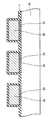
図1に示すように、本実施の形態の半導体装置の製造方法においては、まず、半導体基板10の上にゲート絶縁膜20を形成する。次に、ゲート絶縁膜20の上にゲート電極30を形成する。その後、半導体基板10の表面、ゲート絶縁膜20の側面、ならびに、ゲート電極30の側面および上表面それぞれに沿うように絶縁膜1を形成する。それにより、図1に示す構造が得られる。絶縁膜1を形成する工程においては、化学気相反応および表面反応を利用して、USG(Un-doped Silicate Glass)からなる絶縁膜1を、ゲート電極30とゲート電極30との間の距離の3〜5%の膜厚で堆積させる。 As shown in FIG. 1, in the method for manufacturing a semiconductor device according to the present embodiment, first, a gate
この絶縁膜1を形成する工程(プレデポジション)を行なう目的は、下地である半導体基板10の表面、ゲート絶縁膜20の側面、ならびに、ゲート電極30の側面および上表面を改質することである。そのため、低濃度のO3を含む雰囲気で絶縁膜1を形成することが効果的である。The purpose of performing the step of forming the insulating film 1 (predeposition) is to modify the surface of the
また、絶縁膜1をゲート電極30とゲート電極30との間の距離の5%以上の膜厚に形成すると、ゲート電極30同士の間に形成される絶縁膜1の形状は、オーバーハング形状となってしまう。さらに、ゲート間絶縁膜がオーバーハング形状となってしまうと、その後の成膜ステップにおいて、ゲート電極30同士の間に形成される絶縁膜2に確実にボイドが形成されてしまう。そのため、絶縁膜1の膜厚は、ゲート電極30同士の間の距離の3〜5%の範囲であることが望ましい。 When the
なお、絶縁膜1の詳細な成膜条件は以下に示すとおりである。 The detailed conditions for forming the
成膜の雰囲気中のオゾン(O3)濃度は、0〜3wt%である。また、O3/TEOSのモル比は、0〜3.0である。成膜温度は、450℃〜550℃である。成膜圧力は、200〜600Torr(266〜798hPa)である。キャリアガス種は、不活性ガスの一例としてのHe/N2混合ガスが用いられる。The ozone (O3 ) concentration in the atmosphere for film formation is 0 to3 wt%. Further, the molar ratio of O3 / TEOS is 0 to 3.0. The film forming temperature is 450 ° C. to 550 ° C. The film forming pressure is 200 to 600 Torr (266 to 798 hPa). As a carrier gas type, a He / N2 mixed gas as an example of an inert gas is used.
前述の絶縁膜1を形成した後、図2に示すように、絶縁膜1の表面に沿うように絶縁膜2を形成する工程(メインデポジション)を行なう。絶縁膜2を成膜するときには、絶縁膜1の成膜の場合とは異なり、成膜雰囲気中のオゾン(O3)濃度を8.0〜17.0wt%に変更する。オゾン(O3)濃度の条件を変更するのは、下地の表面または表面近傍において、分子量の大きい中間生成物(Precursor)を形成するためである。これにより、分子量の大きい中間生成物は、流動性があるため、絶縁膜1の上に形成される絶縁膜2が、ゲート電極30の上側部の近傍でオーバーハングしない。After the above-described
なお、絶縁膜2は、BPSG、PSG、BSG、またはUSGからなる。また、絶縁膜2の成膜条件は、次に示すとおりである。 Note that the insulating
成膜温度は、450℃〜550℃である。成膜圧力は、200〜600Torr(266〜798hPa)である。PおよびBのうち少なくともいずれか一方からなる不純物の総濃度は、15wt%以下である。また、O3/TEOSモル比は、3.0〜15.0である。キャリアガス種は、不活性ガスの一例としてのHeガスまたはHe/N2混合ガスが用いられる。また、絶縁膜2の膜厚は、ゲート電極30同士の間の距離の5〜10%である。The film forming temperature is 450 ° C. to 550 ° C. The film forming pressure is 200 to 600 Torr (266 to 798 hPa). The total concentration of impurities composed of at least one of P and B is 15 wt% or less. Further, the O3 / TEOS molar ratio is 3.0 to 15.0. As a carrier gas type, He gas or He / N2 mixed gas is used as an example of an inert gas. The thickness of the insulating
なお、絶縁膜2の成膜時には、絶縁膜2を形成するための反応ガスとしてのTEOS、TEB(Triethyl Borate:(C2H5O)3B)、TEPO(Triethyl Phosphate:(C2H5O)3PO)、およびO3などのガスを反応室内に供給する。When forming the insulating
さらに、絶縁膜2の成膜ステップが完了した後には、絶縁膜2の堆積のための反応ガスの供給を停止するとともに、反応室内の圧力を一定に保つために、反応室内にはO3ではなくO2を送るようにする。それにともなって、TEOS以外のTEBまたはTEPOなどのガスをベントライン(排出用ライン)を使用して反応室以外へ流すか、または、それらのガス(TEBまたはTEPO)の供給をストップする。Further, after the film forming step of the insulating
また、前述のステップの別な態様として、反応室内の圧力を一定に保つために、O3を反応室内に連続的に送り続けるとともに、TEOS、TEB、およびTEPOガスをベントラインに流してもよい。なお、この手法の場合、TEBおよびTEPOガスの反応室への供給をストップしてもよい。In another embodiment of the above-described steps, O3 may be continuously fed into the reaction chamber and TEOS, TEB, and TEPO gases may be supplied to the vent line to keep the pressure in the reaction chamber constant. . In this case, the supply of the TEB and TEPO gases to the reaction chamber may be stopped.
このステップにおいては、連続的なメインデポジションを一時中断することにより、絶縁膜2が下地に吸着した後、吸着面に沿って絶縁膜2が自己平坦化(表面マイグレーション)される。この自己平坦化を十分に行なうためには、メインデポジションを15秒以上中断することが必要である。 In this step, the continuous main deposition is temporarily interrupted, so that the insulating
上述のプリデポジションおよびメインデポジションのステップをゲート電極30同士の間が完全にボイドフリーで埋込まれるまで繰返す。すなわち、絶縁膜2の表面により形成される凹部の底面が、ゲート電極30の上表面よりも高い位置になるまで、絶縁膜1および絶縁膜2を形成する工程を交互に繰返す。それにより、図3に示すように、絶縁膜N−1の上に絶縁膜Nを形成する。なお、Nは自然数である。 The steps of pre-deposition and main deposition described above are repeated until the space between the
また、図3および次に説明する図4には、絶縁膜2の上に絶縁膜N−1が形成されているが、図の描写上の制限から、そのように記載したにすぎず、ゲート電極30の幅と絶縁膜1および絶縁膜2の膜厚との関係により、絶縁膜2と絶縁膜N−1との間には、さらに、何層か絶縁膜が含まれていてもよい。 In addition, in FIG. 3 and FIG. 4 described next, the insulating film N-1 is formed on the insulating
最後に、ゲート電極30同士の間の埋込が完全に終了した後に、次に示す条件で、図4に示すように、絶縁膜Nの上に、膜厚が1.5μm以下のUSG(Un-doped Silicate Glass)からなる絶縁膜N+1の成膜を行なう。 Finally, after the embedding between the
成膜圧力は、成膜レートが大きくなるように、200Torr(266hPa)以下である。成膜温度、O3の濃度、キャリアガス種(不活性ガスの一例としてのHe/N2混合ガス)、およびO3/TEOSのモル比については絶縁膜2の成膜条件と同じである。The film forming pressure is 200 Torr (266 hPa) or less so as to increase the film forming rate. The film forming temperature, O3 concentration, carrier gas type (He / N2 mixed gas as an example of an inert gas), and the molar ratio of O3 / TEOS are the same as the film forming conditions of the insulating
上記のような本実施の形態の半導体装置の製造方法によれば、プリデポジションおよびメインデポジションを繰返すことにより、次のような効果がある。ゲート電極30同士の間が狭い場合においても、ゲート電極30同士の間に良好に絶縁膜の埋込を行なうことができる。また、上記の製造方法によれば、絶縁膜1および2の形成工程においてリフローレスなので、半導体装置の製造工程のサーマルバジェットを抑制することができるため、半導体装置の性能を向上させることができる。 According to the method of manufacturing a semiconductor device of the present embodiment as described above, the following effects are obtained by repeating pre-deposition and main deposition. Even when the space between the
また、下地の表面改質のためのウエットエッチ、プラズマ処理、またはアニールなどの工程が不用であるため、製造工程数を低減することができる。また、最終デポジション膜をUSG膜にすることにより、BPSGに特有の熱処理後の巨大異物(チップキラー異物)の発生を抑制することができる。そのため、後工程において、巨大異物に起因した不良が発生する確率を低減することができるため、半導体装置の歩留りを向上することが可能となる。 Further, since steps such as wet etching, plasma treatment, or annealing for modifying the surface of the base are unnecessary, the number of manufacturing steps can be reduced. Further, by using a USG film as the final deposition film, it is possible to suppress the generation of a large foreign matter (chip killer foreign matter) after heat treatment unique to BPSG. Therefore, in a subsequent process, the probability of occurrence of a defect due to a huge foreign matter can be reduced, so that the yield of semiconductor devices can be improved.
またさらに、上記の製造方法によれば、Bなどの不純物の使用量を削減することにより、B(ボロン同位体10B)などの不純物に起因したシステムのソフトエラーを低減することができる。その結果、半導体装置の歩留まりおよび品質を向上することが可能となる。Furthermore, according to the above-described manufacturing method, it can be reduced by reducing the amount of impurities such as B, B system soft errors due to impurities, such as boron (isotope10 B). As a result, the yield and quality of the semiconductor device can be improved.
なお、今回開示された実施の形態はすべての点で例示であって制限的なものではないと考えられるべきである。本発明の範囲は上記した説明ではなくて特許請求の範囲によって示され、特許請求の範囲と均等の意味および範囲内でのすべての変更が含まれることが意図される。 It should be understood that the embodiments disclosed this time are illustrative in all aspects and not restrictive. The scope of the present invention is defined by the terms of the claims, rather than the description above, and is intended to include any modifications within the scope and meaning equivalent to the terms of the claims.
1,2,N−1,N,N+1 絶縁膜、10 半導体基板、20 ゲート絶縁膜、30 ゲート電極。
1, 2, N-1, N, N + 1 insulating film, 10 semiconductor substrate, 20 gate insulating film, 30 gate electrode.
Claims (15)
Translated fromJapanese前記複数のゲート電極およびゲート絶縁膜、ならびに前記半導体基板それぞれの表面に沿うように第1の絶縁膜を形成する工程と、
前記第1の絶縁膜の上に、該第1の絶縁膜とは異なる第2の絶縁膜を形成する工程とを備え、
前記第1の絶縁膜を形成する工程と前記第2の絶縁膜を形成する工程とを交互に繰返す、半導体装置の製造方法。A method of manufacturing a semiconductor device in which a combination of a plurality of gate electrodes and a gate insulating film is formed on a semiconductor substrate so as to extend in parallel and
Forming a first insulating film along the surface of each of the plurality of gate electrodes and the gate insulating film, and the semiconductor substrate;
Forming a second insulating film different from the first insulating film on the first insulating film;
A method for manufacturing a semiconductor device, wherein a step of forming the first insulating film and a step of forming the second insulating film are alternately repeated.
O3の濃度が0〜3.0wt%であり、
O3/TEOSのモル比が3.0以下であり、
成膜温度が450℃〜550℃であり、
成膜圧力が266〜798hPaであり、かつ、
キャリアガス種が、不活性ガスであるという条件で、形成される、請求項1に記載の半導体装置の製造方法。The first insulating film includes:
The concentration of O3 is 0 to 3.0 wt%,
The molar ratio of O3 / TEOS is 3.0 or less;
A film formation temperature of 450 ° C. to 550 ° C.,
The film forming pressure is 266 to 798 hPa, and
The method for manufacturing a semiconductor device according to claim 1, wherein the carrier gas is formed under a condition that the carrier gas is an inert gas.
第2の絶縁膜はBPSG、PSG、BSG、およびUSGからなる群より選択された1の物質により構成されている、請求項1に記載の半導体装置の製造方法。The first insulating film is made of USG,
The method according to claim 1, wherein the second insulating film is made of one material selected from the group consisting of BPSG, PSG, BSG, and USG.
O3の濃度が8.0〜17.0wt%であり、
O3/TEOSのモル比が3.0〜15.0であり、
成膜温度は450℃〜550℃であり、
成膜圧力は266〜798hPaであり、
PおよびBのうち少なくともいずれか一方からなる不純物の総濃度は15wt%以下であり、かつ、
キャリアガス種が、不活性ガスであるという条件で行なわれる、請求項1に記載の半導体装置の製造方法。The step of forming the second insulating film includes:
The concentration of O3 is 8.0-17.0 wt%,
A molar ratio of O3 / TEOS of 3.0 to 15.0,
The film formation temperature is 450 ° C. to 550 ° C.,
The film forming pressure is 266 to 798 hPa,
The total concentration of impurities consisting of at least one of P and B is 15 wt% or less, and
2. The method for manufacturing a semiconductor device according to claim 1, wherein the method is performed under a condition that a carrier gas species is an inert gas.
前記第2の絶縁膜を堆積する工程の後に、前記複数種類のガスのうち少なくとも1種類のガスは前記チャンバ内へ供給されることが停止され、かつ、前記チャンバ内の圧力が一定に保持されるように前記反応ガスとは異なるガスであって前記第2の絶縁膜の堆積のための反応を生じさせないガスが前記チャンバ内へ流入する、請求項1に記載の半導体装置の製造方法。The second insulating film is deposited using a reaction gas including a plurality of types of gases flowing into the chamber,
After the step of depositing the second insulating film, at least one of the plurality of gases is stopped from being supplied to the chamber, and the pressure in the chamber is kept constant. 2. The method of manufacturing a semiconductor device according to claim 1, wherein a gas which is different from the reaction gas and does not cause a reaction for depositing the second insulating film flows into the chamber.
前記第2の絶縁膜を堆積する工程の後に、前記複数種類のガスのうち少なくとも1種類のガスは前記チャンバ内へ供給されることが停止され、かつ、前記チャンバ内の圧力が一定に保持されるように前記複数種類のガスのうちの少なくとも1種類のガスが前記チャンバ内へ流入し続ける、請求項1に記載の半導体装置の製造方法。The second insulating film is deposited using a reaction gas including a plurality of types of gases flowing into the chamber,
After the step of depositing the second insulating film, at least one of the plurality of gases is stopped from being supplied to the chamber, and the pressure in the chamber is kept constant. 2. The method of manufacturing a semiconductor device according to claim 1, wherein at least one of the plurality of gases continuously flows into the chamber. 3.
前記第2の絶縁膜を堆積する工程の後に、前記複数種類のガスのうち少なくとも1種類のガスは排出用ラインを用いて前記チャンバ外へ流され、かつ、前記チャンバ内の圧力が一定に保持されるように前記反応ガスとは異なるガスであって前記第2の絶縁膜の堆積のための反応を生じさせないガスが前記チャンバ内へ流入する、請求項1に記載の半導体装置の製造方法。The second insulating film is deposited using a reaction gas including a plurality of types of gases flowing into the chamber,
After the step of depositing the second insulating film, at least one of the plurality of gases is flowed out of the chamber using an exhaust line, and the pressure in the chamber is kept constant. 2. The method of manufacturing a semiconductor device according to claim 1, wherein a gas that is different from the reaction gas and does not cause a reaction for depositing the second insulating film flows into the chamber.
前記第2の絶縁膜を堆積する工程の後に、前記複数種類のガスのうち少なくとも1種類のガスは排出用ラインを用いて前記チャンバ外へ流され、かつ、前記チャンバ内の圧力が一定に保持されるように前記複数種類のガスのうちの少なくとも1種類のガスが前記チャンバ内へ流入し続ける、請求項1に記載の半導体装置の製造方法。The second insulating film is deposited using a reaction gas including a plurality of types of gases flowing into the chamber,
After the step of depositing the second insulating film, at least one of the plurality of gases is flowed out of the chamber using an exhaust line, and the pressure in the chamber is kept constant. 2. The method of manufacturing a semiconductor device according to claim 1, wherein at least one of the plurality of gases continues to flow into the chamber so as to be performed.
成膜圧力が266hPa以下であり、
O3の濃度が8.0〜17.0wt%であり、
O3/TEOSのモル比が3.0〜15.0であり、
成膜温度は450℃〜550℃であり、かつ
キャリアガス種は、不活性ガスであるという条件で行なわれる、請求項12に記載の半導体装置の製造方法。The step of forming the third insulating film includes:
The film forming pressure is 266 hPa or less;
The concentration of O3 is 8.0-17.0 wt%,
A molar ratio of O3 / TEOS of 3.0 to 15.0,
The method of manufacturing a semiconductor device according to claim 12, wherein the film formation temperature is 450 ° C. to 550 ° C., and the carrier gas is an inert gas.
Priority Applications (7)
| Application Number | Priority Date | Filing Date | Title |
|---|---|---|---|
| JP2003347115AJP2004214610A (en) | 2002-12-20 | 2003-10-06 | Method for manufacturing semiconductor device |
| TW092133290ATWI238491B (en) | 2002-12-20 | 2003-11-27 | Method of manufacturing semiconductor device |
| KR1020030087107AKR20040055576A (en) | 2002-12-20 | 2003-12-03 | Method of manufacturing semiconductor device |
| DE10356796ADE10356796A1 (en) | 2002-12-20 | 2003-12-04 | Manufacturing method of a semiconductor device |
| US10/733,233US20040121543A1 (en) | 2002-12-20 | 2003-12-12 | Method of manufacturing semiconductor device |
| CNA200310123140XACN1510734A (en) | 2002-12-20 | 2003-12-19 | Manufacturing method of semiconductor device |
| US11/495,663US20060264017A1 (en) | 2002-12-20 | 2006-07-31 | Method of manufacturing semiconductor device |
Applications Claiming Priority (2)
| Application Number | Priority Date | Filing Date | Title |
|---|---|---|---|
| JP2002370025 | 2002-12-20 | ||
| JP2003347115AJP2004214610A (en) | 2002-12-20 | 2003-10-06 | Method for manufacturing semiconductor device |
Publications (1)
| Publication Number | Publication Date |
|---|---|
| JP2004214610Atrue JP2004214610A (en) | 2004-07-29 |
Family
ID=32599292
Family Applications (1)
| Application Number | Title | Priority Date | Filing Date |
|---|---|---|---|
| JP2003347115AWithdrawnJP2004214610A (en) | 2002-12-20 | 2003-10-06 | Method for manufacturing semiconductor device |
Country Status (6)
| Country | Link |
|---|---|
| US (2) | US20040121543A1 (en) |
| JP (1) | JP2004214610A (en) |
| KR (1) | KR20040055576A (en) |
| CN (1) | CN1510734A (en) |
| DE (1) | DE10356796A1 (en) |
| TW (1) | TWI238491B (en) |
Cited By (3)
| Publication number | Priority date | Publication date | Assignee | Title |
|---|---|---|---|---|
| JP2007103754A (en)* | 2005-10-06 | 2007-04-19 | Ran Technical Service Kk | Method for manufacturing cvd film and electronic device |
| KR100950469B1 (en)* | 2007-03-26 | 2010-03-31 | 주식회사 하이닉스반도체 | Method of forming interlayer insulating film of semiconductor device |
| JP2013222717A (en)* | 2012-04-12 | 2013-10-28 | Denso Corp | Semiconductor device and semiconductor device manufacturing method |
Families Citing this family (3)
| Publication number | Priority date | Publication date | Assignee | Title |
|---|---|---|---|---|
| KR100675895B1 (en)* | 2005-06-29 | 2007-02-02 | 주식회사 하이닉스반도체 | Metal wiring structure of semiconductor device and manufacturing method |
| KR20080062024A (en)* | 2006-12-29 | 2008-07-03 | 동부일렉트로닉스 주식회사 | Method for manufacturing semiconductor device and its structure |
| JP6267624B2 (en)* | 2014-10-24 | 2018-01-24 | 住友電気工業株式会社 | Silicon carbide semiconductor device |
Family Cites Families (41)
| Publication number | Priority date | Publication date | Assignee | Title |
|---|---|---|---|---|
| US4855804A (en)* | 1987-11-17 | 1989-08-08 | Motorola, Inc. | Multilayer trench isolation process and structure |
| US4871689A (en)* | 1987-11-17 | 1989-10-03 | Motorola Inc. | Multilayer trench isolation process and structure |
| US5314845A (en)* | 1989-09-28 | 1994-05-24 | Applied Materials, Inc. | Two step process for forming void-free oxide layer over stepped surface of semiconductor wafer |
| US5164337A (en)* | 1989-11-01 | 1992-11-17 | Matsushita Electric Industrial Co., Ltd. | Method of fabricating a semiconductor device having a capacitor in a stacked memory cell |
| US5288325A (en)* | 1991-03-29 | 1994-02-22 | Nec Corporation | Chemical vapor deposition apparatus |
| US5436186A (en)* | 1994-04-22 | 1995-07-25 | United Microelectronics Corporation | Process for fabricating a stacked capacitor |
| US5763286A (en)* | 1994-09-14 | 1998-06-09 | Micron Semiconductor, Inc. | Process for manufacturing a DRAM capacitor having an annularly-grooved, cup-shaped storage-node plate which stores charge on inner and outer surfaces |
| US5656536A (en)* | 1996-03-29 | 1997-08-12 | Vanguard International Semiconductor Corporation | Method of manufacturing a crown shaped capacitor with horizontal fins for high density DRAMs |
| US5849635A (en)* | 1996-07-11 | 1998-12-15 | Micron Technology, Inc. | Semiconductor processing method of forming an insulating dielectric layer and a contact opening therein |
| JPH1092810A (en)* | 1996-09-10 | 1998-04-10 | Mitsubishi Electric Corp | Semiconductor device |
| US5963840A (en)* | 1996-11-13 | 1999-10-05 | Applied Materials, Inc. | Methods for depositing premetal dielectric layer at sub-atmospheric and high temperature conditions |
| US5879574A (en)* | 1996-11-13 | 1999-03-09 | Applied Materials, Inc. | Systems and methods for detecting end of chamber clean in a thermal (non-plasma) process |
| US5812403A (en)* | 1996-11-13 | 1998-09-22 | Applied Materials, Inc. | Methods and apparatus for cleaning surfaces in a substrate processing system |
| US5935334A (en)* | 1996-11-13 | 1999-08-10 | Applied Materials, Inc. | Substrate processing apparatus with bottom-mounted remote plasma system |
| US6347636B1 (en)* | 1996-11-13 | 2002-02-19 | Applied Materials, Inc. | Methods and apparatus for gettering fluorine from chamber material surfaces |
| US5994209A (en)* | 1996-11-13 | 1999-11-30 | Applied Materials, Inc. | Methods and apparatus for forming ultra-shallow doped regions using doped silicon oxide films |
| US5935340A (en)* | 1996-11-13 | 1999-08-10 | Applied Materials, Inc. | Method and apparatus for gettering fluorine from chamber material surfaces |
| US6444037B1 (en)* | 1996-11-13 | 2002-09-03 | Applied Materials, Inc. | Chamber liner for high temperature processing chamber |
| US6114216A (en)* | 1996-11-13 | 2000-09-05 | Applied Materials, Inc. | Methods for shallow trench isolation |
| US6019848A (en)* | 1996-11-13 | 2000-02-01 | Applied Materials, Inc. | Lid assembly for high temperature processing chamber |
| US5968587A (en)* | 1996-11-13 | 1999-10-19 | Applied Materials, Inc. | Systems and methods for controlling the temperature of a vapor deposition apparatus |
| US5939831A (en)* | 1996-11-13 | 1999-08-17 | Applied Materials, Inc. | Methods and apparatus for pre-stabilized plasma generation for microwave clean applications |
| US5873781A (en)* | 1996-11-14 | 1999-02-23 | Bally Gaming International, Inc. | Gaming machine having truly random results |
| US6096654A (en)* | 1997-09-30 | 2000-08-01 | Siemens Aktiengesellschaft | Gapfill of semiconductor structure using doped silicate glasses |
| US6121164A (en)* | 1997-10-24 | 2000-09-19 | Applied Materials, Inc. | Method for forming low compressive stress fluorinated ozone/TEOS oxide film |
| US6360685B1 (en)* | 1998-05-05 | 2002-03-26 | Applied Materials, Inc. | Sub-atmospheric chemical vapor deposition system with dopant bypass |
| US6218268B1 (en)* | 1998-05-05 | 2001-04-17 | Applied Materials, Inc. | Two-step borophosphosilicate glass deposition process and related devices and apparatus |
| KR100319185B1 (en)* | 1998-07-31 | 2002-01-04 | 윤종용 | Method for forming dielectric layer |
| US6239002B1 (en)* | 1998-10-19 | 2001-05-29 | Taiwan Semiconductor Manufacturing Company | Thermal oxidizing method for forming with attenuated surface sensitivity ozone-teos silicon oxide dielectric layer upon a thermally oxidized silicon substrate layer |
| US6090714A (en)* | 1998-10-23 | 2000-07-18 | Taiwan Semiconductor Manufacturing Company | Chemical mechanical polish (CMP) planarizing trench fill method employing composite trench fill layer |
| KR100322531B1 (en)* | 1999-01-11 | 2002-03-18 | 윤종용 | Method for Trench Isolation using a Dent free layer &Semiconductor Device thereof |
| US6297128B1 (en)* | 1999-01-29 | 2001-10-02 | Vantis Corporation | Process for manufacturing shallow trenches filled with dielectric material having low mechanical stress |
| US6090675A (en)* | 1999-04-02 | 2000-07-18 | Taiwan Semiconductor Manufacturing Company | Formation of dielectric layer employing high ozone:tetraethyl-ortho-silicate ratios during chemical vapor deposition |
| KR100323832B1 (en)* | 1999-08-25 | 2002-02-07 | 윤종용 | Method for manufacturing capacitor having high storage capacitance and method for fabricating semiconductor device using the same |
| US6506690B1 (en)* | 2000-04-25 | 2003-01-14 | Agere Systems Inc. | Method for forming dielectric stack including second dielectric layer with lower undoped portion and upper doped portion |
| US6753270B1 (en)* | 2000-08-04 | 2004-06-22 | Applied Materials Inc. | Process for depositing a porous, low dielectric constant silicon oxide film |
| US6489254B1 (en)* | 2000-08-29 | 2002-12-03 | Atmel Corporation | Method of forming pre-metal dielectric film on a semiconductor substrate including first layer of undoped oxide of high ozone:TEOS volume ratio and second layer of low ozone doped BPSG |
| TW479315B (en)* | 2000-10-31 | 2002-03-11 | Applied Materials Inc | Continuous depostiton process |
| US6333277B1 (en)* | 2000-11-29 | 2001-12-25 | Vanguard International Semiconductor Corporation | Method for reducing non-homogenous density during forming process of borophosphosilicate glass layer |
| US6399443B1 (en)* | 2001-05-07 | 2002-06-04 | Chartered Semiconductor Manufacturing Ltd | Method for manufacturing dual voltage flash integrated circuit |
| KR100403630B1 (en)* | 2001-07-07 | 2003-10-30 | 삼성전자주식회사 | Method for forming inter-layer dielectric film of semiconductor device by HDP CVD |
- 2003
- 2003-10-06JPJP2003347115Apatent/JP2004214610A/ennot_activeWithdrawn
- 2003-11-27TWTW092133290Apatent/TWI238491B/ennot_activeIP Right Cessation
- 2003-12-03KRKR1020030087107Apatent/KR20040055576A/ennot_activeCeased
- 2003-12-04DEDE10356796Apatent/DE10356796A1/ennot_activeCeased
- 2003-12-12USUS10/733,233patent/US20040121543A1/ennot_activeAbandoned
- 2003-12-19CNCNA200310123140XApatent/CN1510734A/enactivePending
- 2006
- 2006-07-31USUS11/495,663patent/US20060264017A1/ennot_activeAbandoned
Cited By (3)
| Publication number | Priority date | Publication date | Assignee | Title |
|---|---|---|---|---|
| JP2007103754A (en)* | 2005-10-06 | 2007-04-19 | Ran Technical Service Kk | Method for manufacturing cvd film and electronic device |
| KR100950469B1 (en)* | 2007-03-26 | 2010-03-31 | 주식회사 하이닉스반도체 | Method of forming interlayer insulating film of semiconductor device |
| JP2013222717A (en)* | 2012-04-12 | 2013-10-28 | Denso Corp | Semiconductor device and semiconductor device manufacturing method |
Also Published As
| Publication number | Publication date |
|---|---|
| US20060264017A1 (en) | 2006-11-23 |
| CN1510734A (en) | 2004-07-07 |
| DE10356796A1 (en) | 2004-07-15 |
| KR20040055576A (en) | 2004-06-26 |
| TWI238491B (en) | 2005-08-21 |
| US20040121543A1 (en) | 2004-06-24 |
| TW200419704A (en) | 2004-10-01 |
Similar Documents
| Publication | Publication Date | Title |
|---|---|---|
| JP4733261B2 (en) | Method for reducing unwanted insulator etching due to increased boron concentration | |
| US20060264017A1 (en) | Method of manufacturing semiconductor device | |
| KR20040100767A (en) | method for forming low pressure-silicon nitride layer | |
| KR100562541B1 (en) | Method of forming a SiO / TEOS interlayer dielectric post-treated with a CD silicon oxynitride layer | |
| US7846850B2 (en) | Method of fabricating insulation layer and method of fabricating semiconductor device using the same | |
| US20020127883A1 (en) | Bis (tertiarybutylamino) silane and ozone based doped and undoped oxides | |
| US8735292B2 (en) | Semiconductor processing methods | |
| JP2000058646A (en) | Manufacture of semiconductor device | |
| JP2000183051A (en) | Semiconductor device manufacturing method and semiconductor device | |
| KR100596277B1 (en) | Semiconductor element and insulating film formation method thereof | |
| JPH04343456A (en) | Manufacture of semiconductor device | |
| US12278137B2 (en) | Manufacturing method of semiconductor structure and semiconductor structure | |
| JPH06216122A (en) | Method for manufacturing semiconductor device | |
| JPH08203890A (en) | Formation of interlayer insulation film in semiconductor device | |
| US20080067685A1 (en) | Semiconductor Device Manufacturing Method | |
| KR100392896B1 (en) | Method for forming a semiconductor metal line | |
| KR100871368B1 (en) | Method for manufacturing bit line spacer of semiconductor device | |
| KR100237748B1 (en) | Method for manufacturing interlayer insulator of semiconductor device | |
| KR100351982B1 (en) | Manufacturing method for insulator flim on semiconductor device | |
| JP2001345322A (en) | Method for manufacturing semiconductor device | |
| KR20020041582A (en) | Method for forming interlayer dielectrics of semiconductor device and method for fabricating semiconductor device using the same | |
| KR19980052402A (en) | Metal wiring formation method of semiconductor device | |
| KR20090132784A (en) | Method for Forming PMD of Semiconductor Device | |
| KR19980043736A (en) | Method of forming interlayer insulating film of semiconductor device | |
| KR20030078548A (en) | Method for forming a contact plug in semiconductor device |
Legal Events
| Date | Code | Title | Description |
|---|---|---|---|
| A300 | Application deemed to be withdrawn because no request for examination was validly filed | Free format text:JAPANESE INTERMEDIATE CODE: A300 Effective date:20070109 |