JP2004207711A - Exposure apparatus, exposure method, and device manufacturing method - Google Patents
Exposure apparatus, exposure method, and device manufacturing methodDownload PDFInfo
- Publication number
- JP2004207711A JP2004207711AJP2003412585AJP2003412585AJP2004207711AJP 2004207711 AJP2004207711 AJP 2004207711AJP 2003412585 AJP2003412585 AJP 2003412585AJP 2003412585 AJP2003412585 AJP 2003412585AJP 2004207711 AJP2004207711 AJP 2004207711A
- Authority
- JP
- Japan
- Prior art keywords
- liquid
- substrate
- exposure
- optical system
- projection optical
- Prior art date
- Legal status (The legal status is an assumption and is not a legal conclusion. Google has not performed a legal analysis and makes no representation as to the accuracy of the status listed.)
- Granted
Links
Images


Classifications
- G—PHYSICS
- G03—PHOTOGRAPHY; CINEMATOGRAPHY; ANALOGOUS TECHNIQUES USING WAVES OTHER THAN OPTICAL WAVES; ELECTROGRAPHY; HOLOGRAPHY
- G03F—PHOTOMECHANICAL PRODUCTION OF TEXTURED OR PATTERNED SURFACES, e.g. FOR PRINTING, FOR PROCESSING OF SEMICONDUCTOR DEVICES; MATERIALS THEREFOR; ORIGINALS THEREFOR; APPARATUS SPECIALLY ADAPTED THEREFOR
- G03F7/00—Photomechanical, e.g. photolithographic, production of textured or patterned surfaces, e.g. printing surfaces; Materials therefor, e.g. comprising photoresists; Apparatus specially adapted therefor
- G03F7/70—Microphotolithographic exposure; Apparatus therefor
- G03F7/70216—Mask projection systems
- G03F7/70341—Details of immersion lithography aspects, e.g. exposure media or control of immersion liquid supply
Landscapes
- Physics & Mathematics (AREA)
- General Physics & Mathematics (AREA)
- Exposure And Positioning Against Photoresist Photosensitive Materials (AREA)
- Exposure Of Semiconductors, Excluding Electron Or Ion Beam Exposure (AREA)
Abstract
Translated fromJapaneseDescription
Translated fromJapanese本発明は、投影光学系と基板との間の少なくとも一部を液体で満たした状態で投影光学系によって投影したパターン像で露光する露光装置及び露光方法、並びにデバイス製造方法に関するものである。 The present invention relates to an exposure apparatus, an exposure method, and a device manufacturing method for exposing with a pattern image projected by a projection optical system while at least a part between the projection optical system and a substrate is filled with a liquid.
半導体デバイスや液晶表示デバイスは、マスク上に形成されたパターンを感光性の基板上に転写する、いわゆるフォトリソグラフィの手法により製造される。このフォトリソグラフィ工程で使用される露光装置は、マスクを支持するマスクステージと基板を支持する基板ステージとを有し、マスクステージ及び基板ステージを逐次移動しながらマスクのパターンを投影光学系を介して基板に転写するものである。近年、デバイスパターンのより一層の高集積化に対応するために投影光学系の更なる高解像度化が望まれている。投影光学系の解像度は、使用する露光波長が短くなるほど、また投影光学系の開口数が大きいほど高くなる。そのため、露光装置で使用される露光波長は年々短波長化しており、投影光学系の開口数も増大している。そして、現在主流の露光波長は、KrFエキシマレーザの248nmであるが、更に短波長のArFエキシマレーザの193nmも実用化されつつある。また、露光を行う際には、解像度と同様に焦点深度(DOF)も重要となる。解像度R、及び焦点深度δはそれぞれ以下の式で表される。
R=k1・λ/NA … (1)
δ=±k2・λ/NA2 … (2)
ここで、λは露光波長、NAは投影光学系の開口数、k1、k2はプロセス係数である。(1)式、(2)式より、解像度Rを高めるために、露光波長λを短くして、開口数NAを大きくすると、焦点深度δが狭くなることが分かる。A semiconductor device and a liquid crystal display device are manufactured by a so-called photolithography technique of transferring a pattern formed on a mask onto a photosensitive substrate. The exposure apparatus used in this photolithography process has a mask stage that supports a mask and a substrate stage that supports a substrate, and sequentially moves the mask stage and the substrate stage to project a pattern of the mask through a projection optical system. This is to be transferred to a substrate. In recent years, further improvement in the resolution of the projection optical system has been desired in order to cope with higher integration of device patterns. The resolution of the projection optical system increases as the exposure wavelength used decreases and as the numerical aperture of the projection optical system increases. For this reason, the exposure wavelength used in the exposure apparatus is becoming shorter year by year, and the numerical aperture of the projection optical system is also increasing. The exposure wavelength currently mainstream is 248 nm of KrF excimer laser, but 193 nm of shorter wavelength ArF excimer laser is also being put to practical use. When performing exposure, the depth of focus (DOF) becomes important as well as the resolution. The resolution R and the depth of focus δ are respectively represented by the following equations.
R = k1 · λ / NA (1)
δ = ± k2 · λ / NA2 (2)
Here, λ is the exposure wavelength, NA is the numerical aperture of the projection optical system, and k1 and k2 are the process coefficients. From the expressions (1) and (2), it can be seen that when the exposure wavelength λ is shortened and the numerical aperture NA is increased in order to increase the resolution R, the depth of focus δ becomes narrower.
焦点深度δが狭くなり過ぎると、投影光学系の像面に対して基板表面を合致させることが困難となり、露光動作時のフォーカスマージンが不足する恐れがある。そこで、実質的に露光波長を短くして、且つ焦点深度を広くする方法として、例えば国際公開第99/49504号公報に開示されている液浸法が提案されている。この液浸法は、投影光学系の下面と基板表面との間を水や有機溶媒等の液体で満たし、液体中での露光光の波長が、空気中の1/n(nは液体の屈折率で通常1.2〜1.6程度)になることを利用して解像度を向上するとともに、焦点深度を約n倍に拡大するというものである。
ところで、投影光学系と基板との間に液体を流しながら露光する場合や、投影光学系と基板との間に液体を満たした状態で投影光学系に対して基板を移動しながら露光する場合、投影光学系や基板に対して液体が剥離する可能性があり、基板に転写されるパターン像が劣化するといった不都合が生じる。あるいは、投影光学系と基板との間で液体を流しながら露光する場合にその液体の流れに乱流が生じた場合もパターン像が劣化する。 By the way, when performing exposure while flowing a liquid between the projection optical system and the substrate, or when performing exposure while moving the substrate to the projection optical system in a state where the liquid is filled between the projection optical system and the substrate, There is a possibility that the liquid may be peeled off from the projection optical system or the substrate, and the pattern image transferred to the substrate may be deteriorated. Alternatively, when exposure is performed while a liquid flows between the projection optical system and the substrate, the pattern image also deteriorates when turbulence occurs in the flow of the liquid.
本発明はこのような事情に鑑みてなされたものであって、投影光学系と基板との間に液体を満たして露光処理する際、液体を所望の状態に配置して精度良くパターンを転写できる露光装置及び露光方法、並びにデバイス製造方法を提供することを目的とする。 The present invention has been made in view of such circumstances, and when performing exposure processing by filling a liquid between a projection optical system and a substrate, a liquid can be arranged in a desired state and a pattern can be accurately transferred. An object of the present invention is to provide an exposure apparatus, an exposure method, and a device manufacturing method.
上記の課題を解決するため、本発明は実施の形態に示す図1〜図10に対応付けした以下の構成を採用している。 In order to solve the above-described problems, the present invention employs the following configurations corresponding to FIGS. 1 to 10 shown in the embodiments.
本発明の第1の態様に従えば、パターンの像を液体(50)を介して基板(P)上に転写して基板を露光する露光装置であって:
前記パターンの像を基板に投影する投影光学系(PL)を備え、
前記投影光学系(PL)の前記液体(50)と接触する部分(60、PK)は、液体(50)との親和性を調整するために表面処理されている露光装置(EX)が提供される。According to a first aspect of the present invention, there is provided an exposure apparatus for exposing a substrate by transferring an image of a pattern onto a substrate (P) via a liquid (50):
A projection optical system (PL) for projecting an image of the pattern onto a substrate,
An exposure apparatus (EX) is provided in which a portion (60, PK) of the projection optical system (PL) that comes into contact with the liquid (50) is surface-treated to adjust the affinity with the liquid (50). You.
本発明の露光装置では、液体投影光学系の液体と接触する部分(以下、適宜、「液体接触部分」という)に、液体との親和性を調整するための表面処理が施されているので、投影光学系と基板との間に液体が所望の状態で維持される。例えば、液体接触部分の液体との親和性が低ぎる場合、前記接触する部分と液体とが剥離したり、あるいは気泡が発生するなどの液浸露光に悪影響を及ぼす現象が生じる。一方、液体接触部分の液体との親和性が高すぎる場合、液体が前記接触する部分に対して過剰に濡れ拡がって投影光学系と基板との間から流出する等の不都合が生じる場合がある。これに対して、本発明の露光装置では、投影光学系の液体接触部分の液体との親和性が調整されているために、露光中に基板が露光光に対して静止されている一括露光のみならず、露光中に基板が移動ステージにより移動される走査型露光装置であっても、液浸状態が確実に基板と投影光学系との間に維持される。 In the exposure apparatus of the present invention, a portion of the liquid projection optical system that comes into contact with the liquid (hereinafter, appropriately referred to as a “liquid contact portion”) is subjected to a surface treatment for adjusting the affinity with the liquid. The liquid is maintained in a desired state between the projection optical system and the substrate. For example, when the affinity of the liquid contact portion with the liquid is low, a phenomenon that adversely affects the immersion exposure, such as separation of the contact portion from the liquid or generation of bubbles, occurs. On the other hand, if the affinity of the liquid contact portion with the liquid is too high, there may be a problem that the liquid excessively spreads on the contact portion and flows out from between the projection optical system and the substrate. On the other hand, in the exposure apparatus of the present invention, since the affinity of the liquid contact portion of the projection optical system with the liquid is adjusted, only the batch exposure in which the substrate is stationary with respect to the exposure light during the exposure is performed. However, even in a scanning exposure apparatus in which the substrate is moved by the moving stage during exposure, the liquid immersion state is reliably maintained between the substrate and the projection optical system.
本発明の第2の態様に従えば、パターンの像を液体(50)を介して基板(P)上に転写して基板を露光する露光装置であって:
前記パターンの像を基板に投影する投影光学系(PL)を備え;
前記投影光学系(PL)が、その先端の光学素子(60)表面を含む第1表面領域(AR1)と、第1表面領域(AR1)周辺の第2表面領域(AR2)とを有し、第1表面領域(AR1)の液体(50)に対する親和性が、第2表面領域(AR2)の液体(50)に対する親和性よりも高い露光装置(EX)が提供される。According to a second aspect of the present invention, there is provided an exposure apparatus for exposing a substrate by transferring an image of a pattern onto a substrate (P) via a liquid (50):
A projection optical system (PL) for projecting an image of the pattern onto a substrate;
The projection optical system (PL) has a first surface area (AR1) including a surface of an optical element (60) at a tip thereof, and a second surface area (AR2) around the first surface area (AR1), An exposure apparatus (EX) is provided in which the affinity of the first surface region (AR1) for the liquid (50) is higher than the affinity of the second surface region (AR2) for the liquid (50).
本発明によれば、投影光学系の先端の光学素子を含む第1表面領域の液体に対する親和性を、その周辺の第2表面領域より高くすることで、第1表面領域により露光光の光路上では液体が安定して配置されるとともに、第2表面領域により液体が周囲に濡れ拡がらず外部に流出しない。したがって、露光中に基板が露光光に対して静止されている一括露光のみならず、露光中に基板が露光光に対して移動される走査型露光であっても、液体を露光光の光路上に安定して配置することができる。 According to the present invention, the first surface area including the optical element at the tip of the projection optical system has higher affinity for liquid than the surrounding second surface area, so that the first surface area allows the exposure light to be on the optical path. In this case, the liquid is stably disposed, and the liquid does not spread to the surroundings and flow to the outside due to the second surface region. Therefore, not only in the batch exposure in which the substrate is stationary with respect to the exposure light during the exposure, but also in the scanning exposure in which the substrate is moved with respect to the exposure light during the exposure, the liquid is placed on the optical path of the exposure light. Can be arranged stably.
本発明の第3の態様に従えば、露光ビーム(EL)でパターンを照明し、パターンの像を液体(50)を介して基板(P)上に転写して基板を露光する露光装置であって:前記パターンの像を基板に投影する投影光学系(PL)と;投影光学系(PL)と基板(P)との間の少なくとも一部を液体(50)で満たす液浸装置(1、2)とを備え;液体(50)の厚さをd、投影光学系(PL)と基板(P)との間における液体(50)の流れの速度をv、液体(50)の密度をρ、液体(50)の粘性係数をμとして、条件式 (v・d・ρ)/μ≦2000 が満足される露光装置(EX)が提供される。 According to a third aspect of the present invention, there is provided an exposure apparatus for irradiating a pattern with an exposure beam (EL), transferring an image of the pattern onto a substrate (P) via a liquid (50), and exposing the substrate. T: a projection optical system (PL) for projecting an image of the pattern onto a substrate; and an immersion device (1, 2) which fills at least a part between the projection optical system (PL) and the substrate (P) with a liquid (50). 2) the thickness of the liquid (50) is d, the velocity of the flow of the liquid (50) between the projection optical system (PL) and the substrate (P) is v, and the density of the liquid (50) is ρ An exposure apparatus (EX) that satisfies the conditional expression (v · d · ρ) / μ ≦ 2000, where μ is the viscosity coefficient of the liquid (50).
本発明によれば、上記条件式を満足するように、投影光学系(PL)と基板(P)との間の少なくとも一部に液体が維持される条件を設定することにより、液体に乱流が生じない。したがって、液体の乱流に起因して基板に投影されるパターン像が劣化したりするといった不都合を抑えることができる。 According to the present invention, turbulence is generated in the liquid by setting the condition for maintaining the liquid in at least a part between the projection optical system (PL) and the substrate (P) so as to satisfy the above conditional expression. Does not occur. Therefore, it is possible to suppress such a disadvantage that the pattern image projected on the substrate is deteriorated due to the turbulent flow of the liquid.
本発明の第4の態様に従えば、露光ビーム(EL)でマスク(M)のパターンを照明し、パターンの像を液体(50)を介して基板(P)上に転写して基板を露光する露光装置であって:前記パターンの像を基板に投影する投影光学系(PL)と;投影光学系(PL)と基板(P)との間の少なくとも一部を液体で満たすための液浸装置(1、2)とを備え;液体(50)が基板(P)の走査方向と平行に層流となって流れる露光装置(EX)が提供される。 According to the fourth aspect of the present invention, the pattern of the mask (M) is illuminated with the exposure beam (EL), and the image of the pattern is transferred onto the substrate (P) via the liquid (50) to expose the substrate. A projection optical system (PL) for projecting an image of the pattern onto a substrate; and an immersion liquid for filling at least a part between the projection optical system (PL) and the substrate (P) with a liquid. An exposure apparatus (EX) is provided, wherein the liquid (50) flows in a laminar flow parallel to the scanning direction of the substrate (P).
本発明によれば、液浸状態を種々の方法により制御することにより、露光中に液体が基板の走査方向と平行に層流となって流れるので、基板に投影されるパターン像の劣化を防止することができる。また、液体に接する投影光学系やウエハあるいはウエハを保持する基板ステージ等に不要な振動を発生させることもない。例えば、液浸装置の液体供給(回収)量を制御したり、液浸装置の液体供給ノズルの構造を調整したり、あるいは露光時に基板を移動する場合にはその速度を調整することで、液体の流れを層流化することができる。 According to the present invention, by controlling the liquid immersion state by various methods, the liquid flows as a laminar flow parallel to the scanning direction of the substrate during exposure, thereby preventing the pattern image projected on the substrate from deteriorating. can do. Further, unnecessary vibration is not generated in the projection optical system in contact with the liquid, the wafer, or the substrate stage holding the wafer. For example, by controlling the amount of liquid supply (recovery) of the immersion device, adjusting the structure of the liquid supply nozzle of the immersion device, or adjusting the speed of the substrate when moving the substrate during exposure, Can be made laminar.
本発明の第5の態様に従えば、露光ビーム(EL)でパターンを照明し、パターンの像を液体(50)を介して基板(P)上に転写して基板を露光する露光装置であって:前記パターンの像を基板に投影する投影光学系(PL)と;基板(P)上のみに液体(50)を供給する液浸装置(1、2)と;液浸装置(1、2)を制御する制御装置(CONT)とを備え;該制御装置(CONT)は、基板(P)の露光中に液体(50)の供給が停止されるように液浸装置(1、2)を制御する露光装置(EX)が提供される。 According to a fifth aspect of the present invention, there is provided an exposure apparatus for irradiating a pattern with an exposure beam (EL), transferring an image of the pattern onto a substrate (P) via a liquid (50), and exposing the substrate. T: a projection optical system (PL) for projecting the image of the pattern onto a substrate; an immersion device (1, 2) for supplying a liquid (50) only onto the substrate (P); an immersion device (1, 2) A control device (CONT) for controlling the liquid immersion devices (1, 2) such that the supply of the liquid (50) is stopped during the exposure of the substrate (P). An exposure apparatus (EX) for controlling is provided.
本発明によれば、液浸装置が基板の露光中に液体の供給を行わないように制御されることにより、基板上に塗布された感光剤を傷めることがなく、基板上に形成されるパターンの劣化を防止でき、また、投影光学系と基板との位置関係を安定して所望の状態に維持できる。 According to the present invention, the liquid immersion device is controlled so as not to supply the liquid during exposure of the substrate, so that the photosensitive agent applied on the substrate is not damaged, and the pattern formed on the substrate is not damaged. Degradation can be prevented, and the positional relationship between the projection optical system and the substrate can be stably maintained in a desired state.
本発明の第6の態様に従えば、投影光学系(PL)によるパターンの像を基板(P)上に投影して基板(P)を露光する露光方法において:露光前に、基板(P)の表面を、液体(50)との親和性を調整するために表面処理することと;投影光学系(PL)と基板(P)との間の少なくとも一部を液体(50)で満たすことと;
パターンの像を、液体(50)を介して基板(P)上に投影して基板(P)を露光することとを含む露光方法が提供される。According to a sixth aspect of the present invention, in an exposure method for exposing a substrate (P) by projecting an image of a pattern by a projection optical system (PL) onto the substrate (P): Surface treatment for adjusting the affinity with the liquid (50); filling at least a part between the projection optical system (PL) and the substrate (P) with the liquid (50). ;
Exposing the substrate (P) by projecting an image of the pattern onto the substrate (P) via the liquid (50).
本発明によれば、液浸露光が行われる前に、基板の表面に、液体との親和性に応じた表面処理を施すことで、基板上に液体を液浸露光に好適な状態で維持できる。例えば、液体との親和性が低すぎる場合、基板の表面に対して液体が剥離したり、あるいは気泡が発生する等の不都合が生じる。一方、液体との親和性が高すぎる場合、液体が基板上で過剰に濡れ拡がるなどの不都合が生じる場合がある。これに対して、本発明の露光方法のように、液体との親和性を考慮して、基板表面に適当な処理を施すことにより、基板上で液体を所望の状態に保持することができ、また基板上の液体の回収及び除去を適切に行うことができる。 According to the present invention, before immersion exposure is performed, the surface of the substrate is subjected to a surface treatment according to the affinity with the liquid, whereby the liquid can be maintained on the substrate in a state suitable for immersion exposure. . For example, if the affinity with the liquid is too low, inconveniences such as separation of the liquid from the surface of the substrate and generation of bubbles may occur. On the other hand, if the affinity with the liquid is too high, there may be a problem that the liquid excessively spreads on the substrate. On the other hand, as in the exposure method of the present invention, the liquid can be held in a desired state on the substrate by performing an appropriate treatment on the substrate surface in consideration of the affinity with the liquid, In addition, the liquid on the substrate can be appropriately collected and removed.
本発明によれば、液浸露光において、投影光学系と基板との間において、液体の剥離や気泡の発生、あるいは乱流の発生を抑え、液体を所望の状態で維持できるので、広い焦点深度の下でパターン転写を正確に行うことができる。したがって、本発明はArFなどの短波長光源を用いる露光に極めて有用であり、所望の性能を有する高集積化デバイスを製造することができる。 According to the present invention, in liquid immersion exposure, between the projection optical system and the substrate, separation of liquid, generation of bubbles, or generation of turbulence can be suppressed, and the liquid can be maintained in a desired state. Under this condition, pattern transfer can be performed accurately. Therefore, the present invention is extremely useful for exposure using a short-wavelength light source such as ArF, and can manufacture a highly integrated device having desired performance.
以下、本発明の露光装置及びデバイス製造方法について図面を参照しながら説明するが、本発明はこれに限定されない。図1は本発明の露光装置の一実施形態を示す概略構成図である。 Hereinafter, an exposure apparatus and a device manufacturing method of the present invention will be described with reference to the drawings, but the present invention is not limited thereto. FIG. 1 is a schematic configuration diagram showing an embodiment of the exposure apparatus of the present invention.
図1において、露光装置EXは、マスクMを支持するマスクステージMSTと、基板Pを支持する基板ステージPSTと、マスクステージMSTに支持されているマスクMを露光光ELで照明する照明光学系ILと、露光光ELで照明されたマスクMのパターンの像を基板ステージPSTに支持されている基板Pに投影露光する投影光学系PLと、露光装置EX全体の動作を統括制御する制御装置CONTとを備えている。 1, an exposure apparatus EX includes a mask stage MST that supports a mask M, a substrate stage PST that supports a substrate P, and an illumination optical system IL that illuminates the mask M supported by the mask stage MST with exposure light EL. A projection optical system PL for projecting and exposing an image of the pattern of the mask M illuminated by the exposure light EL onto a substrate P supported on a substrate stage PST, and a control device CONT for controlling the overall operation of the exposure apparatus EX. It has.
ここで、本実施形態では、露光装置EXとしてマスクMと基板Pとを走査方向における互いに異なる向き(逆方向)に同期移動しつつマスクMに形成されたパターンを基板Pに露光する走査型露光装置(所謂スキャニングステッパ)を使用する場合を例にして説明する。以下の説明において、投影光学系PLの光軸AXと一致する方向をZ軸方向、Z軸方向に垂直な平面内でマスクMと基板Pとの同期移動方向(走査方向)をX軸方向、Z軸方向及びY軸方向に垂直な方向(非走査方向)をY軸方向とする。また、X軸、Y軸、及びZ軸まわり方向をそれぞれ、θX、θY、及びθZ方向とする。なお、ここでいう「基板」は半導体ウエハ上にレジストを塗布したものを含み、「マスク」は基板上に縮小投影されるデバイスパターンを形成されたレチクルを含む。 Here, in the present embodiment, the exposure apparatus EX scans the mask M and the substrate P synchronously in directions different from each other in the scanning direction (opposite directions) while exposing the pattern formed on the mask M to the substrate P. An example in which an apparatus (a so-called scanning stepper) is used will be described. In the following description, the direction that coincides with the optical axis AX of the projection optical system PL is the Z-axis direction, the synchronous movement direction (scanning direction) between the mask M and the substrate P in a plane perpendicular to the Z-axis direction is the X-axis direction, A direction perpendicular to the Z-axis direction and the Y-axis direction (non-scanning direction) is defined as a Y-axis direction. In addition, directions around the X axis, the Y axis, and the Z axis are defined as θX, θY, and θZ directions, respectively. Here, the “substrate” includes a semiconductor wafer coated with a resist, and the “mask” includes a reticle on which a device pattern to be reduced and projected onto the substrate is formed.
照明光学系ILは、マスクステージMSTに支持されているマスクMを露光光ELで照明するものであり、露光用光源、露光用光源から射出された光束の照度を均一化するオプティカルインテグレータ、オプティカルインテグレータからの露光光ELを集光するコンデンサレンズ、リレーレンズ系、露光光ELによるマスクM上の照明領域をスリット状に設定する可変視野絞り等を有している。マスクM上の所定の照明領域は照明光学系ILにより均一な照度分布の露光光ELで照明される。照明光学系ILから射出される露光光ELとしては、例えば水銀ランプから射出される紫外域の輝線(g線、h線、i線)及びKrFエキシマレーザ光(波長248nm)等の遠紫外光(DUV光)や、ArFエキシマレーザ光(波長193nm)及びF2レーザ光(波長157nm)等の真空紫外光(VUV光)などが用いられる。本実施形態においては、ArFエキシマレーザ光を用いる。The illumination optical system IL illuminates the mask M supported by the mask stage MST with the exposure light EL, and includes an exposure light source, an optical integrator for equalizing the illuminance of a light beam emitted from the exposure light source, and an optical integrator. A condenser lens, a relay lens system, and a variable field stop for setting an illumination area on the mask M by the exposure light EL in a slit shape. A predetermined illumination area on the mask M is illuminated by the illumination optical system IL with exposure light EL having a uniform illuminance distribution. The exposure light EL emitted from the illumination optical system IL includes, for example, ultraviolet bright lines (g-line, h-line, i-line) emitted from a mercury lamp and far ultraviolet light (KrF excimer laser light (wavelength: 248 nm)). DUV light) and, ArF excimer laser light (wavelength 193 nm) andF 2 laser beam (wavelength 157 nm) vacuum ultraviolet light (VUV light) and the like. In the present embodiment, ArF excimer laser light is used.
マスクステージMSTは、マスクMを支持するものであって、投影光学系PLの光軸AXに垂直な平面内、すなわちXY平面内で2次元移動可能及びθZ方向に微小回転可能である。マスクステージMSTはリニアモータ等のマスクステージ駆動装置MSTDにより駆動される。マスクステージ駆動装置MSTDは制御装置CONTにより制御される。マスクステージMST上のマスクMの2次元方向の位置、及び回転角はレーザ干渉計によりリアルタイムで計測され、計測結果は制御装置CONTに出力される。制御装置CONTはレーザ干渉計の計測結果に基づいてマスクステージ駆動装置MSTDを駆動することでマスクステージMSTに支持されているマスクMの位置決めを行う。 The mask stage MST supports the mask M, and is two-dimensionally movable in a plane perpendicular to the optical axis AX of the projection optical system PL, that is, in an XY plane, and is capable of minute rotation in the θZ direction. The mask stage MST is driven by a mask stage driving device MSTD such as a linear motor. The mask stage driving device MSTD is controlled by the control device CONT. The position and the rotation angle of the mask M on the mask stage MST in the two-dimensional direction are measured in real time by a laser interferometer, and the measurement result is output to the control device CONT. The control device CONT drives the mask stage driving device MSTD based on the measurement result of the laser interferometer to position the mask M supported by the mask stage MST.
投影光学系PLは、マスクMのパターンを所定の投影倍率βで基板Pに投影露光するものであって、複数の光学素子(レンズ)で構成されており、これら光学素子は金属部材、例えばステンレス(SUS403)で形成された鏡筒PKで支持されている。本実施形態において、投影光学系PLは、投影倍率βが例えば1/4あるいは1/5の縮小系である。なお、投影光学系PLは等倍系及び拡大系のいずれでもよい。また、本実施形態の投影光学系PLの基板P側の先端部7には、石英、フッ化カルシウム(蛍石)などのガラス部材から形成された平行平面板(光学素子)60が設けられている。この光学素子60は鏡筒PKに対して着脱(交換)可能に設けられている。投影光学系PLの先端部7は、光学素子60と、これを保持する鏡筒(保持部材)PKの一部により構成されている。 The projection optical system PL is for projecting and exposing the pattern of the mask M onto the substrate P at a predetermined projection magnification β, and includes a plurality of optical elements (lenses). These optical elements are metal members, for example, stainless steel. It is supported by a lens barrel PK made of (SUS403). In the present embodiment, the projection optical system PL is a reduction system in which the projection magnification β is, for example, 4 or 5. Note that the projection optical system PL may be either a unity magnification system or an enlargement system. In addition, a parallel plane plate (optical element) 60 formed of a glass member such as quartz or calcium fluoride (fluorite) is provided at the
基板ステージPSTは、基板Pを支持するものであって、基板Pを基板ホルダを介して保持するZステージ51と、Zステージ51を支持するXYステージ52と、XYステージ52を支持するベース53とを備えている。基板ステージPSTはリニアモータ等の基板ステージ駆動装置PSTDにより駆動される。基板ステージ駆動装置PSTDは制御装置CONTにより制御される。Zステージ51を駆動することにより、Zステージ51に保持されている基板PのZ軸方向における位置(フォーカス位置)、及びθX、θY方向における位置が制御される。また、XYステージ52を駆動することにより、基板PのXY方向における位置(投影光学系PLの像面と実質的に平行な方向の位置)が制御される。すなわち、Zステージ51は、基板Pのフォーカス位置及び傾斜角を制御して基板Pの表面をオートフォーカス方式、及びオートレベリング方式で投影光学系PLの像面に合わせ込み、XYステージ52は基板PのX軸方向及びY軸方向における位置決めを行う。なお、ZステージとXYステージとを一体的に設けてよいことは言うまでもない。 The substrate stage PST supports the substrate P, and includes a
基板ステージPST(Zステージ51)上には、基板ステージPSTとともに投影光学系PLに対して移動する移動鏡54が設けられている。また、移動鏡54に対向する位置にはレーザ干渉計55が設けられている。基板ステージPST上の基板Pの2次元方向の位置、及び回転角はレーザ干渉計55によりリアルタイムで計測され、計測結果は制御装置CONTに出力される。制御装置CONTはレーザ干渉計55の計測結果に基づいて基板ステージ駆動装置PSTDを駆動することで基板ステージPSTに支持されている基板Pの位置決めを行う。 On the substrate stage PST (Z stage 51), a
本実施形態では、露光波長を実質的に短くして解像度を向上するとともに、焦点深度を実質的に広くするために、液浸法を適用する。そのため、少なくともマスクMのパターンの像を基板P上に転写している間は、基板Pの表面と投影光学系PLの先端部7との間に所定の液体50が満たされる。上述したように、投影光学系PLの先端部7には光学素子60及び鏡筒PKの一部が配置されており、液体50は光学素子(ガラス部材)60と、鏡筒(金属部材)PKとに接触する。本実施形態において、液体50には純水が用いられる。純水は、ArFエキシマレーザ光のみならず、露光光ELを例えば水銀ランプから射出される紫外域の輝線(g線、h線、i線)及びKrFエキシマレーザ光(波長248nm)等の遠紫外光(DUV光)とした場合、この露光光ELを透過可能である。 In the present embodiment, the immersion method is applied to improve the resolution by substantially shortening the exposure wavelength and substantially widen the depth of focus. Therefore, the
露光装置EXは、投影光学系PLの先端部7と基板Pとの間の空間56に所定の液体50を供給する液体供給装置(液浸装置、供給装置)1と、空間56の液体50を回収する液体回収装置(液浸装置、回収装置)2とを備えている。液体供給装置1は、投影光学系PLと基板Pとの間の少なくとも一部に、基板Pの走査方向と平行に液体50を流すものであって、液体50を収容するタンク、加圧ポンプなどを備えている。液体供給装置1には供給管3の一端部が接続され、供給管3の他端部には供給ノズル4が接続されている。液体供給装置1は供給管3及び供給ノズル4を介して空間56に液体50を供給する。 The exposure apparatus EX includes a liquid supply device (liquid immersion device, supply device) 1 that supplies a
液体回収装置2は、吸引ポンプ、回収した液体50を収容するタンクなどを備えている。液体回収装置2には回収管6の一端部が接続され、回収管6の他端部には回収ノズル5が接続されている。液体回収装置2は回収ノズル5及び回収管6を介して空間56の液体50を回収する。空間56に液体50を満たす際、制御装置CONTは液体供給装置1を駆動し、供給管3及び供給ノズル4を介して空間56に対して単位時間当たり所定量の液体50を供給するとともに、液体回収装置2を駆動し、回収ノズル5及び回収管6を介して単位時間当たり所定量の液体50を空間56より回収する。これにより、投影光学系PLの先端面7と基板Pとの間の空間56に液体50が配置される。 The
走査露光時には、先端面60Aの直下の矩形の投影領域にマスクMの一部のパターン像が投影され、投影光学系PLに対して、マスクMが−X方向(又は+X方向)に速度Vで移動するのに同期して、XYステージ52を介して基板Pが+X方向(又は−X方向)に速度β・V(βは投影倍率)で移動する。そして、1つのショット領域への露光終了後に、基板Pのステッピングによって次のショット領域が走査開始位置に移動し、以下、ステップ・アンド・スキャン方式で各ショット領域に対する露光処理が順次行われる。本実施形態では、基板Pの移動方向と平行に基板の移動方向と同一方向に液体50を流すように設定されている。 At the time of scanning exposure, a part of the pattern image of the mask M is projected onto a rectangular projection area immediately below the
図2は、投影光学系PLの先端部7と、液体50をX軸方向に供給する供給ノズル4(4A〜4C)と、液体50を回収する回収ノズル5(5A、5B)との位置関係を示す図である。図2において、先端部7(光学素子60の先端面60A)の形状はY軸方向に細長い矩形状となっており、投影光学系PLの先端部7をX軸方向に挟むように、+X方向側に3つの供給ノズル4A〜4Cが配置され、−X方向側に2つの回収ノズル5A、5Bが配置されている。そして、供給ノズル4A〜4Cは供給管3を介して液体供給装置1に接続され、回収ノズル5A、5Bは回収管4を介して液体回収装置2に接続されている。また、供給ノズル4A〜4Cと回収ノズル5A、5Bとを先端部7の中心に対して略180°回転した配置に、供給ノズル8A〜8Cと、回収ノズル9A、9Bとが配置されている。供給ノズル4A〜4Cと回収ノズル9A、9BとはY軸方向に交互に配列され、供給ノズル8A〜8Cと回収ノズル5A、5BとはY軸方向に交互に配列され、供給ノズル8A〜8Cは供給管10を介して液体供給装置1に接続され、回収ノズル9A、9Bは回収管11を介して液体回収装置2に接続されている。ノズルからの液体の供給は、投影光学系PLと基板Pとの間に気体部分が生じないように行う必要がある。 FIG. 2 shows the positional relationship between the
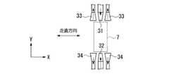
また、図3に示すように、先端部7を挟んでY軸方向両側のそれぞれに供給ノズル31、32及び回収ノズル33、34を設けることもできる。この供給ノズル及び回収ノズルにより、ステップ移動する際の基板Pの非走査方向(Y軸方向)への移動時においても、投影光学系PLと基板Pとの間に液体50を安定して供給することができる。 As shown in FIG. 3,
なお、上述したノズルの形状は特に限定されるものでなく、例えば先端部7の長辺について2対のノズルで液体50の供給又は回収を行うようにしてもよい。なお、この場合には、+X方向、又は−X方向のどちらの方向からも液体50の供給及び回収を行うことができるようにするため、供給ノズルと回収ノズルと上下に並べて配置してもよい。 The shape of the nozzle described above is not particularly limited. For example, the supply or recovery of the liquid 50 may be performed with two pairs of nozzles on the long side of the
図4は、投影光学系PLの先端部7近傍の拡大図である。図4において、投影光学系PLの先端部7には、液体50との親和性に応じた表面処理が施されている。先端部7は、走査露光するために基板Pを走査方向(X軸方向)に移動するときに液体50と接触する部分であって、光学素子60の下面60A及び鏡筒PK下面の一部を含む投影光学系PLの下面7A、及びこの下面7Aに接続する鏡筒PKの一部の側面7Bを含む。本実施形態において、液体50は水であるため、先端部7には水との親和性に応じた表面処理が施されている。 FIG. 4 is an enlarged view of the vicinity of the
投影光学系PLの先端部7において、光学素子60の表面(下面)60A及び鏡筒PKの下面の一部の領域を含む第1表面領域AR1と、この第1表面領域AR1周辺であって鏡筒PKの下面の残りの領域及び鏡筒PKの側面を含む第2表面領域AR2とは、互いに異なる表面処理が施されている。具体的には、第1表面領域AR1の液体(水)50に対する親和性が、第2表面領域AR2の液体(水)50に対する親和性より高くなるように、第1、第2表面領域AR1、AR2のそれぞれに対して表面処理が施されている。ここでは、光学素子60を含む第1表面領域AR1に対しては親液性を付与する親液化処理(親水化処理)、第2表面領域AR2に対しては撥液性を付与する撥液化処理(撥水化処理)が施されている。親液化処理とは液体に対する親和性を高くする処理であり、撥液化処理とは液体に対する親和性を低くする処理である。 At the
表面処理は液体50の極性に応じて行われる。本実施形態において、液体50は極性の大きい水であるため、光学素子60を含む第1表面領域AR1に対する親水化処理として、例えばアルコールなど極性の大きい分子構造の物質で薄膜を形成することで、この第1表面領域AR1に対して親水性を付与する。あるいは、第1表面領域AR1の光学素子60の下面60A及び鏡筒PKに対して、例えば処理ガスとして酸素(O2)を用いてプラズマ処理するO2プラズマ処理を施すことによって表面に極性の強いO分子が多く集まるため親水性を付与することができる。このように、液体50として水を用いる場合には第1表面領域AR1にOH基など極性の大きい分子構造を持ったものを表面に配置させる処理が望ましい。また、第1表面領域AR1は、ガラス部材である光学素子60と金属部材である鏡筒PKとを含んでいるため、親水化処理する場合、ガラス部材と金属部材とのそれぞれに異なる物質で薄膜を形成するなど、異なる表面処理を行うことができる。もちろん、第1表面領域AR1のガラス部材及び金属部材のそれぞれに対して同じ表面処理を施してもよい。また、薄膜を形成する場合には、塗布や蒸着などの手法を用いることができる。The surface treatment is performed according to the polarity of the liquid 50. In the present embodiment, since the liquid 50 is water having high polarity, the first surface region AR1 including the
一方、鏡筒PK表面を含む第2表面領域AR2に対しては撥水化処理が施される。第2表面領域AR2に対する撥水化処理として、例えばフッ素を含む極性の小さい分子構造の物質で薄膜を形成することで、この第2表面領域AR2に対して撥水性を付与する。あるいは、処理ガスとして四フッ化炭素(CF4)を用いてプラズマ処理するCF4プラズマ処理を施すことによって撥水性を付与することができる。第2表面領域AR2に対して薄膜を形成する場合においても、塗布や蒸着などの手法を用いることができる。On the other hand, the second surface area AR2 including the surface of the lens barrel PK is subjected to a water-repellent treatment. As the water-repellent treatment for the second surface region AR2, for example, a water-repellent property is imparted to the second surface region AR2 by forming a thin film using a substance having a molecular structure having a small polarity including fluorine. Alternatively, water repellency can be imparted by performing CF4 plasma treatment in which plasma treatment is performed using carbon tetrafluoride (CF4 ) as a treatment gas. Even when a thin film is formed on the second surface region AR2, a method such as coating or vapor deposition can be used.
また、本実施形態では、基板Pの表面にも、液体50との親和性に合わせて表面処理が施されている。ここでは、基板Pの表面に対して親水化処理が施されている。基板Pに対する親水化処理としては、上述したような例えばアルコールなど極性の大きい分子構造の物質で薄膜を形成することで基板Pの表面に対して親液性を付与する。なお、基板Pの表面をアルコールなどを塗布して表面処理した場合には、露光後であって次の感光材料の塗布の前工程、例えば、ディベロッパ/コーターに基板を搬送する前に、塗膜を洗浄するための洗浄工程を設けることが望ましい。 In the present embodiment, the surface of the substrate P is also subjected to a surface treatment in accordance with the affinity with the liquid 50. Here, the surface of the substrate P is subjected to a hydrophilic treatment. In the hydrophilization treatment for the substrate P, the surface of the substrate P is made lyophilic by forming a thin film with a substance having a molecular structure having a large polarity such as alcohol as described above. In the case where the surface of the substrate P is subjected to a surface treatment by applying alcohol or the like, after the exposure and before the application of the next photosensitive material, for example, before the substrate is transported to the developer / coater, the coating film It is desirable to provide a cleaning step for cleaning the substrate.
そして、第1表面領域AR1の液体50に対する親和性を、第2表面領域AR2の液体50に対する親和性よりも高くすることによって、液体50が第1表面領域AR1内で安定して保持される。 Then, by making the affinity of the first surface region AR1 for the liquid 50 higher than the affinity of the second surface region AR2 for the liquid 50, the liquid 50 is stably held in the first surface region AR1.
ここで、表面処理のための薄膜は、液体50に対して非溶解性の材料により形成される。また、光学素子60に形成される薄膜は、露光光ELの光路上に配置されるものであるため、露光光ELに対して透過性を有する材料で形成され、その膜厚も露光光ELを透過可能な程度に設定される。 Here, the thin film for the surface treatment is formed of a material that is insoluble in the liquid 50. Further, since the thin film formed on the
次に、上述した露光装置EXを用いてマスクMのパターンを基板Pに露光する際の作用について説明する。 Next, an operation of exposing the pattern of the mask M to the substrate P using the above-described exposure apparatus EX will be described.
マスクMがマスクステージMSTにロードされるとともに、基板Pが基板ステージPSTにロードされたら、制御装置CONTは液体供給装置1を駆動し、空間56に対する液体供給動作を開始する。液体供給装置1は空間56に対して基板Pの移動方向に沿って液体50を供給する。例えば、矢印Xa(図2参照)で示す走査方向(−X方向)に基板Pを移動させて走査露光を行う場合には、供給管3、供給ノズル4A〜4C、回収管4、及び回収ノズル5A、5Bを用いて、液体供給装置1及び液体回収装置2により液体50の供給及び回収が行われる。すなわち、基板Pが−X方向に移動する際には、供給管3及び供給ノズル4(4A〜4C)を介して液体供給装置1から液体50が投影光学系PLと基板Pとの間に供給されるとともに、回収ノズル5(5A、5B)、及び回収管6を介して液体50が液体回収装置2に回収され、レンズ60と基板Pとの間を満たすように−X方向に液体50が流れる。一方、矢印Xbで示す走査方向(+X方向)に基板Pを移動させて走査露光を行う場合には、供給管10、供給ノズル8A〜8C、回収管11、及び回収ノズル9A、9Bを用いて、液体供給装置1及び液体回収装置2により液体50の供給及び回収が行われる。すなわち、基板Pが+X方向に移動する際には、供給管10及び供給ノズル8(8A〜8C)を介して液体供給装置1から液体50が投影光学系PLと基板Pとの間に供給されるとともに、回収ノズル9(9A、9B)、及び回収管11を介して液体50が液体回収装置2に回収され、レンズ60と基板Pとの間を満たすように+X方向に液体50が流れる。このように、制御装置CONTは、液体供給装置1及び液体回収装置2を用いて基板Pの移動方向に沿って液体50を流す。この場合、例えば液体供給装置1から供給ノズル4を介して供給される液体50は基板Pの−X方向への移動に伴って空間56に引き込まれるようにして流れるので、液体供給装置1の供給エネルギーが小さくても液体50を空間56に容易に供給できる。そして、走査方向に応じて液体50を流す方向を切り替えることにより、+X方向、又は−X方向のどちらの方向に基板Pを走査する場合にも、レンズ60の先端面7と基板Pとの間を液体50で満たすことができ、高い解像度及び広い焦点深度を得ることができる。 When the mask M is loaded on the mask stage MST and the substrate P is loaded on the substrate stage PST, the control device CONT drives the
このとき、投影光学系PLや基板Pに表面処理が施されていない場合について考える。図5は表面処理が施されていない状態での液体50の流れを示す模式図である。ここでは、投影光学系PL表面や基板P表面は液体50に対して親和性が低いものとする。 At this time, a case where the surface treatment is not performed on the projection optical system PL and the substrate P is considered. FIG. 5 is a schematic diagram showing the flow of the liquid 50 in a state where the surface treatment has not been performed. Here, it is assumed that the surface of the projection optical system PL and the surface of the substrate P have low affinity for the liquid 50.
図5(a)は基板ステージPSTが停止している状態を示す図である。液体50は供給ノズル4より供給され、回収ノズル5より回収される。このとき、液体50と基板Pとは親和性が低いため、接触角θは大きい。図5(b)は基板Pが基板ステージPSTによりX軸方向に移動を開始した状態を示す図である。液体50は移動する基板Pに引っ張られるようにして変形する。液体50と基板Pとは親和性が低いため、液体50は基板Pの表面から離れやすい。図5(c)は基板ステージPST上の基板Pの移動速度が更に上昇した状態を示す図である。基板Pと液体50との間に剥離領域(気泡)H1が形成され、しかも光学素子60と液体50との間にも剥離領域H2が形成される。この剥離領域H1、H2が露光光ELの光路上に形成されると、マスクMのパターンが基板Pに正確に転写されない。 FIG. 5A is a diagram illustrating a state where the substrate stage PST is stopped. The liquid 50 is supplied from the
図6は、図4を用いて説明したように投影光学系Pの先端部7及び基板P表面が表面処理されている状態での液体50の流れを示す模式図である。 FIG. 6 is a schematic diagram showing the flow of the liquid 50 in a state where the
図6(a)は基板ステージPSTが停止している状態を示す図である。表面処理を施して液体50と基板Pとの親和性を高めたので、接触角θは小さい。図6(b)は基板Pが基板ステージPSTによりX軸方向に移動を開始した状態を示す図である。液体50と基板Pとの親和性は高いので、基板Pが移動しても液体50は基板Pに過剰に引っ張られない。また、投影光学系PLの第1表面領域AR1の液体50に対する親和性も高いので、第1表面領域AR1と液体50とは剥離しない。このとき、第1表面領域AR1の周辺は、液体50に対する親和性が低い第2表面領域AR2で囲まれているので、空間56の液体50は外部に流出することなく、空間56に安定して配置されている。図6(c)は基板ステージPST上の基板Pの移動速度が更に上昇した状態を示す図である。基板Pの移動速度を上昇しても、投影光学系PL及び基板Pに対して表面処理が施されているので、液体50と投影光学系PL及び基板Pとの間で剥離は生じない。 FIG. 6A is a diagram illustrating a state where the substrate stage PST is stopped. Since the surface treatment is performed to increase the affinity between the liquid 50 and the substrate P, the contact angle θ is small. FIG. 6B is a diagram illustrating a state where the substrate P has started moving in the X-axis direction by the substrate stage PST. Since the affinity between the liquid 50 and the substrate P is high, the liquid 50 is not excessively pulled by the substrate P even when the substrate P moves. Further, since the first surface region AR1 of the projection optical system PL has a high affinity for the liquid 50, the first surface region AR1 and the liquid 50 do not separate. At this time, since the periphery of the first surface area AR1 is surrounded by the second surface area AR2 having low affinity for the liquid 50, the liquid 50 in the
以上説明したように、液浸法に基づく露光処理において、液体50と接触する部分である投影光学系PLの先端部7や基板Pの表面に、液体50との親和性に応じた表面処理を施すことで、液体50の剥離や気泡の発生等といった不都合の発生を抑え、投影光学系PLと基板Pとの間に液体50を安定して配置できる。したがって、良好なパターン転写精度を維持できる。 As described above, in the exposure processing based on the liquid immersion method, the surface treatment according to the affinity with the liquid 50 is performed on the
なお、液体50との親和性に応じた表面処理は、投影光学系PLの先端部7と基板P表面のどちから一方だけに施すようにしてもよい。
また、上記実施形態において、光学素子60の表面60A及び鏡筒(保持部材)PKの下面一部を第1表面領域AR1とし、この第1表面領域AR1に対して液体50に対する親和性が高くなるように表面処理が施されるように説明した。すなわち、親液化処理領域と撥液化処理領域との境界が鏡筒PK下面にあるように説明したが、この境界は光学素子60表面に設定されていてもよい。すなわち、光学素子60の一部の領域(少なくとも露光光が通過する領域)に親液化処理が施され、残りの領域に撥液化処理が施されるといった構成でもよい。もちろん、親液化処理領域と撥液化処理領域との境界を、光学素子60と鏡筒PKとの境界に一致させてもよい。すなわち、親液化処理を光学素子60のみに対して行う構成でもよい。更には、上記境界は投影光学系PLの下面7Aに設定することに限らず、投影光学系PLの下面7A全部を親液化処理してもよい。The surface treatment according to the affinity with the liquid 50 may be performed on only one of the
In the above embodiment, the
更に、表面処理を行う際、親液性(撥液性)に分布を持たせることも可能である。換言すれば、表面処理する面上の複数の領域についての液体の接触角がそれぞれ異なる値となるように表面処理を行うことができる。あるいは、親液化領域と撥液化領域とを適宜分割して配置するようにしてもよい。 Further, when performing the surface treatment, it is also possible to impart a distribution to the lyophilicity (liquid repellency). In other words, the surface treatment can be performed so that the contact angles of the liquids on a plurality of regions on the surface to be surface treated have different values. Alternatively, the lyophilic region and the lyophobic region may be appropriately divided and arranged.
また、表面処理のための薄膜は単層膜であってもよいし複数の層からなる膜であってもよい。また、その形成材料も、金属、金属化合物、及び有機物など、所望の性能を発揮できる材料であれば任意の材料を用いることができる。 Further, the thin film for the surface treatment may be a single-layer film or a film having a plurality of layers. Further, as a material for forming the material, any material such as a metal, a metal compound, and an organic material can be used as long as the material can exhibit desired performance.
また、光学素子60や基板Pの表面処理には薄膜形成やプラズマ処理等が有効であるが、金属部材である鏡筒PKの表面処理に関しては、例えばこの鏡筒PKの表面を粗面処理するなど物理的手法で液体に対する親和性を調整できる。 In addition, thin film formation, plasma processing, or the like is effective for the surface treatment of the
なお、上述の実施形態においては、投影光学系PLと基板Pとの間における液体の安定した保持を重視して基板P表面を親液化(親液処理)しているが、基板P表面からの液体の回収や除去を重視する場合には、基板P表面を撥液化(撥液処理)してもよい。
また上述の実施形態においては、液体50との親和性に応じた表面処理を、投影光学系PLの先端部7および基板Pの表面に施すようにしているが、投影光学系PLの先端部7と基板P表面の少なくとも一方との親和性に応じた液体を液体供給装置1から供給するようにしてもよい。In the above-described embodiment, the surface of the substrate P is made lyophilic (lyophilic treatment) with an emphasis on the stable holding of the liquid between the projection optical system PL and the substrate P. When importance is attached to the collection and removal of the liquid, the surface of the substrate P may be made lyophobic (lyophobic treatment).
In the above-described embodiment, the surface treatment according to the affinity with the liquid 50 is performed on the
上述したように、本実施形態における液体50は純水により構成されている。純水は、半導体製造工場等で容易に大量に入手できるとともに、基板P上のフォトレジストや光学素子(レンズ)等に対する悪影響がない利点がある。また、純水は環境に対する悪影響がないとともに、不純物の含有量が極めて低いため、基板Pの表面、及び投影光学系PLの先端面に設けられている光学素子の表面を洗浄する作用も期待できる。 As described above, the liquid 50 in the present embodiment is made of pure water. Pure water has the advantage that it can be easily obtained in large quantities at a semiconductor manufacturing plant or the like, and that there is no adverse effect on the photoresist on the substrate P, optical elements (lenses), and the like. In addition, since pure water has no adverse effect on the environment and has a very low impurity content, an effect of cleaning the surface of the substrate P and the surface of the optical element provided on the tip end surface of the projection optical system PL can be expected. .
そして、波長が193nm程度の露光光ELに対する純水(水)の屈折率nはほぼ1.44〜1.47程度と言われており、露光光ELの光源としてArFエキシマレーザ光(波長193nm)を用いた場合、基板P上では1/n、すなわち131〜134nm程度に短波長化されて高い解像度が得られる。更に、焦点深度は空気中に比べて約n倍、すなわち1.44〜1.47倍程度に拡大されるため、空気中で使用する場合と同程度の焦点深度が確保できればよい場合には、投影光学系PLの開口数をより増加させることができ、この点でも解像度が向上する。 The refractive index n of pure water (water) with respect to the exposure light EL having a wavelength of about 193 nm is said to be approximately 1.44 to 1.47, and an ArF excimer laser light (wavelength of 193 nm) is used as a light source of the exposure light EL. Is used, the wavelength is shortened to 1 / n, that is, about 131 to 134 nm on the substrate P, and a high resolution is obtained. Further, since the depth of focus is expanded to about n times, that is, about 1.44 to 1.47 times as compared with that in the air, if it is sufficient to secure the same depth of focus as when using in air, The numerical aperture of the projection optical system PL can be further increased, and the resolution is also improved in this regard.
本実施形態では、投影光学系PLの先端に光学素子60として平行平面板が取り付けられているが、投影光学系PLの先端に取り付ける光学素子としては、投影光学系PLの光学特性、例えば収差(球面収差、コマ収差等)の調整に用いる光学プレートであってもよしレンズであってもよい。一方、液体50と接触する光学素子を、レンズより安価な平行平面板とすることにより、露光装置EXの運搬、組立、調整時等において投影光学系PLの透過率、基板P上での露光光ELの照度、及び照度分布の均一性を低下させる物質(例えばシリコン系有機物等)がその平行平面板に付着しても、液体50を供給する直前にその平行平面板を交換するだけでよく、液体50と接触する光学素子をレンズとする場合に比べてその交換コストが低くなるという利点がある。すなわち、露光光ELの照射によりレジストから発生する飛散粒子、または液体50中の不純物の付着などに起因して液体50に接触する光学素子の表面が汚れるため、その光学素子を定期的に交換する必要があるが、この光学素子を安価な平行平面板とすることにより、レンズに比べて交換部品のコストが低く、且つ交換に要する時間を短くすることができ、メンテナンスコスト(ランニングコスト)の上昇やスループットの低下を抑えることができる。 In the present embodiment, a parallel flat plate is attached to the tip of the projection optical system PL as the
また、液体50の流れによって生じる投影光学系PLの先端の光学素子と基板Pとの間の圧力が大きい場合には、その光学素子を交換可能とするのではなく、その圧力によって光学素子が動かないように堅固に固定してもよい。 When the pressure between the optical element at the tip of the projection optical system PL and the substrate P caused by the flow of the liquid 50 is large, the optical element is not replaced but the optical element is moved by the pressure. It may be fixed firmly so that it does not occur.
なお、本実施形態の液体50は水であるが、水以外の液体であってもよい、例えば、露光光ELの光源がF2レーザである場合、このF2レーザ光は水を透過しないので、液体50としてはF2レーザ光を透過可能な例えばフッ素系オイル(フッ素系の液体)や過フッ化ポリエーテル(PFPE)であってもよい。この場合、投影光学系PLの液体50と接触する部分や基板P表面には、例えばフッ素を含む極性の小さい分子構造の物質で薄膜を形成することで親液化処理する。また、液体50としては、その他にも、露光光ELに対する透過性があってできるだけ屈折率が高く、投影光学系PLや基板P表面に塗布されているフォトレジストに対して安定なもの(例えばセダー油)を用いることも可能である。この場合も表面処理は用いる液体50の極性に応じて行われる。The liquid 50 of the present embodiment is water, a liquid other than water may be, for example, when the light source of exposure light EL is an F2 laser, the F2 laser beam is not transmitted through water as the liquid 50 may be permeable such as a fluorine-containing oil F2 laser beam (fluorine-based liquid) or perfluoropolyether (PFPE). In this case, the portion of the projection optical system PL that comes into contact with the liquid 50 or the surface of the substrate P is subjected to lyophilic treatment by forming a thin film with a substance having a small polar molecular structure including, for example, fluorine. In addition, as the liquid 50, a liquid that has transparency to the exposure light EL, has a refractive index as high as possible, and is stable with respect to the photoresist applied to the projection optical system PL and the surface of the substrate P (for example, Cedar) Oil) can also be used. Also in this case, the surface treatment is performed according to the polarity of the liquid 50 to be used.
次に、本発明の第2実施形態について図7を参照しながら説明する。 Next, a second embodiment of the present invention will be described with reference to FIG.
本実施形態の露光装置EXでは、投影光学系PLの下面7Aと基板P表面との間における液体50の厚さ(ここでは、投影光学系PLと基板Pとの間隔)をd、投影光学系PLと基板Pとの間における液体50の流れの速度をv、液体50の密度をρ、液体50の粘性係数をμとした場合、条件式
(v・d・ρ)/μ≦2000 …(3)
を満足するように設定されている。これにより、空間56において液体50は層流となって流れる。なお、液体50中においては、その液体中の位置に応じて異なる複数の流れの速度vが存在することも考えられるが、その最大速度Vmaxが上記(3)式を満たせばよい。In the exposure apparatus EX of the present embodiment, the thickness of the liquid 50 (here, the distance between the projection optical system PL and the substrate P) between the
Is set to satisfy. Accordingly, the liquid 50 flows in the
上記条件式(3)を満足するように、制御装置CONTは、液体供給装置1による空間56に対する液体の単位時間当たりの供給量と、液体回収装置2による空間56の液体の単位時間当たりの回収量とのうち少なくともいずれか一方を調整する。これにより、空間56を流れる液体50の速度vが決定され、条件式(3)を満足することができる。条件式(3)を満足することで液体50は空間56を層流となって流れる。 In order to satisfy the conditional expression (3), the control device CONT controls the supply amount of the liquid to the
あるいは、制御装置CONTは、基板ステージPSTを介して基板Pの走査方向への移動速度を調整することによっても、条件式(3)を満足することができる。すなわち、空間56を流れる液体50の速度vは基板Pの移動速度で決定されることもある。すなわち、基板P上の液体50が基板Pの移動によって基板Pに引きずられるようにして流れる可能性もある。その場合は、基板Pの移動速度を調整することで条件式(3)を満足することができる。例えば、基板Pと液体50とがほぼ同じ速度で投影光学系PLに対して流れる場合には、基板Pの移動速度を液体50の速度vとして、条件式(3)を満足するようにすればよい。この場合においても、液体50は空間56を層流となって流れる。またその場合には、基板Pの露光中に、必ずしも液体供給装置1および液体回収装置2を動作させる必要がなく、基板Pの移動速度の調整のみで液体50の流れを層流化することができる。 Alternatively, the control device CONT can also satisfy the conditional expression (3) by adjusting the moving speed of the substrate P in the scanning direction via the substrate stage PST. That is, the speed v of the liquid 50 flowing through the
なお、上記条件式(3)を満足させるために、液体50の厚さ(すなわち投影光学系PLと基板Pとの間の距離)dを露光装置の設計値として予め設定し、これに基づいて速度vを決定してもよいし、速度vを設計値として予め設定し、これに基づいて厚さ(距離)dを決定するようにしてもよい。 In order to satisfy the conditional expression (3), the thickness d of the liquid 50 (that is, the distance between the projection optical system PL and the substrate P) is set in advance as a design value of the exposure apparatus, and based on this, The speed v may be determined, or the speed v may be set in advance as a design value, and the thickness (distance) d may be determined based on this.
また、空間56において液体50が層流となって流れるようにするために、例えば図8(a)に示すように、液体供給装置1に接続する供給ノズル4の開口部にスリットを設けたり、図8(b)に示すように、供給ノズル4の開口部に多孔質体を設けることで液体50を整流し層流状態で流すことができる。 In order to allow the liquid 50 to flow in a laminar flow in the
そして、液体50が層流となって流れることにより、圧力の変動による屈折率変化や振動といった不都合が抑制され、良好なパターン転写精度を維持できる。更に、投影光学系PLのうち液体50と接触する部分や基板P表面に表面処理を施すとともに、露光装置EXを上記条件式(3)を満足するように設定して露光処理することで、空間56の液体50はパターン転写精度に影響を与えないより一層良好な状態に設定される。 In addition, since the liquid 50 flows in a laminar flow, inconveniences such as a change in refractive index and vibration due to a change in pressure are suppressed, and good pattern transfer accuracy can be maintained. Further, a surface treatment is performed on a portion of the projection optical system PL that comes into contact with the liquid 50 and on the surface of the substrate P, and the exposure apparatus EX is set so as to satisfy the above conditional expression (3) to perform the exposure processing, thereby providing a space. The liquid 50 of 56 is set to a better state without affecting the pattern transfer accuracy.
上述の実施形態においては、投影光学系PLと基板Pとの間を局所的に液体で満たす露光装置を採用しているが、露光対象の基板を保持したステージを液槽の中で移動させる液浸露光装置や、ステージ上に所定深さの液体槽を形成しその中に基板を保持する液浸露光装置にも本発明を適用可能である。露光対象の基板を保持したステージを液槽の中で移動させる液浸露光装置の構造及び露光動作については、例えば特開平6−124873号公報に、ステージ上に所定深さの液体槽を形成しその中に基板を保持する液浸露光装置の構造及び露光動作については、例えば特開平10−303114号公報や米国特許第5,825,043号にそれぞれ開示されている。 In the above-described embodiment, the exposure apparatus that locally fills the space between the projection optical system PL and the substrate P with the liquid is used. However, the liquid that moves the stage holding the substrate to be exposed in the liquid tank is used. The present invention is also applicable to an immersion exposure apparatus or an immersion exposure apparatus in which a liquid tank having a predetermined depth is formed on a stage and a substrate is held therein. Regarding the structure and exposure operation of an immersion exposure apparatus that moves a stage holding a substrate to be exposed in a liquid tank, for example, Japanese Patent Application Laid-Open No. 6-124873 discloses a liquid tank having a predetermined depth formed on a stage. The structure and exposure operation of a liquid immersion exposure apparatus that holds a substrate therein are disclosed in, for example, JP-A-10-303114 and US Pat. No. 5,825,043.
なお、上記実施形態においては、液体供給装置1及び液体回収装置2により前記基板Pの露光中にも液体50の供給及び回収を継続していたが、基板Pの露光中は液体供給装置1及び液体回収装置2による液体50の供給及び回収を停止するようにしてもよい。すなわち、基板Pの露光開始前に、投影光学系PLの先端部7と基板Pとの間に、投影光学系PLのワーキングディスタンス以下(0.5〜1.0mm程度)の厚さの液浸部分ができる程度に、あるいは、基板Pの全面に薄い液膜ができる程度に、少量の液体50を液体供給装置1により基板P上に供給し、その液体50を介して投影光学系PLの先端部7と基板Pとを密着する。投影光学系PLの先端部7と基板Pとの間隔が数mm以下なので、基板Pの露光中に、液体供給装置1及び液体回収装置2による液体の供給及び回収を行わずに基板Pを移動しても、液体50の表面張力により投影光学系PLと基板Pとの間に液体を50を保持し続けることができる。また、液体供給装置1からの液体供給によって基板P上のレジスト(感光膜)が傷むこともない。この場合、基板Pの周縁に所定幅で液体50をはじくコーティング(液体が水の場合は撥水コート)を施しておくと、基板P上から液体50が流出するのを防ぐことができる。なお、基板Pを移動する場合には、上述の条件式(3)を満たすようにして液体50に乱流を発生させないようにすることは言うまでもない。 In the above-described embodiment, the supply and the recovery of the liquid 50 are continued during the exposure of the substrate P by the
また、上述の実施形態では、基板ステージPST上で液体(50)の供給を行ったが、基板ステージPST上に基板Pが搬入される前に基板P上に液体を供給してもよい。この場合、基板P上の一部もしくは全面に供給される液体の厚さを0.5〜1.0mm程度にすれば表面張力によって液体を基板P上に載せたまま基板ステージPSTへの搬入、基板ステージPSTからの搬出を行うことができる。またこの場合も、基板Pの周縁に所定幅の撥液コーティングを施しておけば、基板P上での液体の保持力を高めることができる。このように、基板P上に液体を保持したまま、基板ステージPSTへの基板Pの搬入及び基板ステージPSTからの基板Pの搬出を行うことによって、基板ステージPST上で液体の供給及び回収を行う機構を省くことができる。 In the above-described embodiment, the liquid (50) is supplied on the substrate stage PST. However, the liquid may be supplied on the substrate P before the substrate P is loaded onto the substrate stage PST. In this case, if the thickness of the liquid supplied to a part or the whole surface of the substrate P is set to about 0.5 to 1.0 mm, the liquid is loaded onto the substrate stage PST while being placed on the substrate P by surface tension, Unloading from the substrate stage PST can be performed. Also in this case, if a liquid-repellent coating having a predetermined width is applied to the peripheral edge of the substrate P, the liquid holding force on the substrate P can be increased. As described above, while the liquid is held on the substrate P, the supply and recovery of the liquid are performed on the substrate stage PST by carrying in the substrate P to the substrate stage PST and carrying out the substrate P from the substrate stage PST. The mechanism can be omitted.
なお、上記実施形態では、投影光学系PLと基板P表面との間は液体50で満たされている構成であるが、例えば、図9に示すように、基板Pの表面に平行平面板からなるカバーガラス65を取り付けた状態で液体50を満たす構成であってもよい。ここで、カバーガラス65は支持部材66を介してZステージ51上で支持されており、カバーガラス65、支持部材66、及びZステージ51で形成される空間57は略密閉空間である。そして、この空間57内部に液体50及び基板Pが配置されている。カバーガラス65は露光光ELに対して透過性を有する材料により構成されている。そして、カバーガラス65の表面と投影光学系PLとの間の空間56’に対して、液体供給装置1及び液体回収装置2による液体50の供給及び回収が行われ、カバーガラス65の表面と投影光学系PLの先端部7とを間隔をdとした場合、空間56’において上記条件式(3)を満足するように設定されている。 In the above embodiment, the space between the projection optical system PL and the surface of the substrate P is configured to be filled with the liquid 50. For example, as shown in FIG. The liquid 50 may be filled with the
そして、このカバーガラス65の表面(上面)に対しても、液体50との親和性に応じた表面処理を施すことができる。カバーガラス65の表面は親液化処理されることが望ましいため、液体50が水である場合、カバーガラス65の表面には極性の大きい分子構造の物質で薄膜が形成される。 The surface (upper surface) of the
なお、上記各実施形態の基板Pとしては、半導体デバイス製造用の半導体ウエハのみならず、ディスプレイデバイス用のガラス基板や、薄膜磁気ヘッド用のセラミックウエハ、あるいは露光装置で用いられるマスクまたはレチクルの原版(合成石英、シリコンウエハ)等が適用される。 The substrate P in each of the above embodiments is not limited to a semiconductor wafer for manufacturing a semiconductor device, but also a glass substrate for a display device, a ceramic wafer for a thin-film magnetic head, or an original mask or reticle used in an exposure apparatus. (Synthetic quartz, silicon wafer) and the like are applied.
露光装置EXとしては、マスクMと基板Pとを同期移動してマスクMのパターンを走査露光するステップ・アンド・スキャン方式の走査型露光装置(スキャニングステッパ)の他に、マスクMと基板Pとを静止した状態でマスクMのパターンを一括露光し、基板Pを順次ステップ移動させるステップ・アンド・リピート方式の投影露光装置(ステッパ)にも適用することができる。また、本発明は基板P上で少なくとも2つのパターンを部分的に重ねて転写するステップ・アンド・スティッチ方式の露光装置にも適用できる。 The exposure apparatus EX includes a step-and-scan type scanning exposure apparatus (scanning stepper) that scans and exposes the pattern of the mask M by synchronously moving the mask M and the substrate P. Can be applied to a step-and-repeat type projection exposure apparatus (stepper) in which the pattern of the mask M is exposed collectively while the substrate is stationary, and the substrate P is sequentially moved stepwise. The present invention is also applicable to a step-and-stitch type exposure apparatus that transfers at least two patterns on the substrate P while partially overlapping each other.
また、本発明は、ツインステージ型の露光装置にも適用できる。ツインステージ型の露光装置の構造及び露光動作は、例えば特開平10−163099号及び特開平10−214783号(対応米国特許6,341,007号、6,400,441号、6,549,269号及び6,590,634号)、特表2000−505958号(対応米国特許5,969,441号)あるいは米国特許6,208,407号に開示されている。 The present invention is also applicable to a twin-stage type exposure apparatus. The structure and exposure operation of a twin-stage type exposure apparatus are described in, for example, JP-A-10-163099 and JP-A-10-214783 (corresponding to U.S. Pat. Nos. 6,341,007, 6,400,441, 6,549,269). And 6,590,634), JP-T-2000-505958 (corresponding U.S. Pat. No. 5,969,441) or U.S. Pat. No. 6,208,407.
露光装置EXの種類としては、基板Pに半導体素子パターンを露光する半導体素子製造用の露光装置に限られず、液晶表示素子製造用又はディスプレイ製造用の露光装置や、薄膜磁気ヘッド、撮像素子(CCD)あるいはレチクル又はマスクなどを製造するための露光装置などにも広く適用できる。 The type of the exposure apparatus EX is not limited to an exposure apparatus for manufacturing a semiconductor element for exposing a semiconductor element pattern onto the substrate P, but may be an exposure apparatus for manufacturing a liquid crystal display element or a display, a thin film magnetic head, an imaging element (CCD). ) Or an exposure apparatus for manufacturing a reticle or a mask.
基板ステージPSTやマスクステージMSTにリニアモータを用いる場合は、エアベアリングを用いたエア浮上型およびローレンツ力またはリアクタンス力を用いた磁気浮上型のどちらを用いてもよい。また、各ステージPST、MSTは、ガイドに沿って移動するタイプでもよく、ガイドを設けないガイドレスタイプであってもよい。ステージにリニアモータを用いた例は、米国特許5,623,853及び5,528,118に開示されている。 When a linear motor is used for the substrate stage PST or the mask stage MST, any of an air levitation type using an air bearing and a magnetic levitation type using Lorentz force or reactance force may be used. Each of the stages PST and MST may be of a type that moves along a guide, or may be a guideless type that does not have a guide. Examples using a linear motor for the stage are disclosed in U.S. Patents 5,623,853 and 5,528,118.
各ステージPST、MSTの駆動機構としては、二次元に磁石を配置した磁石ユニットと、二次元にコイルを配置した電機子ユニットとを対向させ電磁力により各ステージPST、MSTを駆動する平面モータを用いてもよい。この場合、磁石ユニットと電機子ユニットとのいずれか一方をステージPST、MSTに接続し、磁石ユニットと電機子ユニットとの他方をステージPST、MSTの移動面側に設ければよい。 As a driving mechanism of each stage PST, MST, a planar motor that drives each stage PST, MST by electromagnetic force by facing a magnet unit having a two-dimensionally arranged magnet and an armature unit having a two-dimensionally arranged coil. May be used. In this case, one of the magnet unit and the armature unit may be connected to the stages PST and MST, and the other of the magnet unit and the armature unit may be provided on the moving surface side of the stages PST and MST.
基板ステージPSTの移動により発生する反力は、投影光学系PLに伝わらないように、フレーム部材を用いて機械的に床(大地)に逃がしてもよい。この反力の処理方法は、例えば特開平8−166475号公報(米国特許5,528,118)に詳細に開示されている。 The reaction force generated by the movement of the substrate stage PST may be mechanically released to the floor (ground) using a frame member so as not to be transmitted to the projection optical system PL. The method of processing this reaction force is disclosed in detail, for example, in Japanese Patent Application Laid-Open No. 8-166475 (US Pat. No. 5,528,118).
マスクステージMSTの移動により発生する反力は、投影光学系PLに伝わらないように、フレーム部材を用いて機械的に床(大地)に逃がしてもよい。この反力の処理方法は、例えば特開平8−330224号公報(米国特許第5,874,820号)に詳細に開示されている。 The reaction force generated by the movement of the mask stage MST may be mechanically released to the floor (ground) using a frame member so as not to be transmitted to the projection optical system PL. The method of processing this reaction force is disclosed in detail, for example, in Japanese Patent Application Laid-Open No. 8-330224 (U.S. Pat. No. 5,874,820).
以上のように、本願実施形態の露光装置EXは、本願特許請求の範囲に挙げられた各構成要素を含む各種サブシステムを、所定の機械的精度、電気的精度、光学的精度を保つように、組み立てることで製造される。これら各種精度を確保するために、この組み立ての前後には、各種光学系については光学的精度を達成するための調整、各種機械系については機械的精度を達成するための調整、各種電気系については電気的精度を達成するための調整が行われる。各種サブシステムから露光装置への組み立て工程は、各種サブシステム相互の、機械的接続、電気回路の配線接続、気圧回路の配管接続等が含まれる。この各種サブシステムから露光装置への組み立て工程の前に、各サブシステム個々の組み立て工程があることはいうまでもない。各種サブシステムの露光装置への組み立て工程が終了したら、総合調整が行われ、露光装置全体としての各種精度が確保される。なお、露光装置の製造は温度およびクリーン度等が管理されたクリーンルームで行うことが望ましい。 As described above, the exposure apparatus EX according to the embodiment of the present invention controls various subsystems including the respective components described in the claims of the present application so as to maintain predetermined mechanical accuracy, electrical accuracy, and optical accuracy. Manufactured by assembling. Before and after this assembly, adjustments to achieve optical accuracy for various optical systems, adjustments to achieve mechanical accuracy for various mechanical systems, and various electric systems to ensure these various accuracy Are adjusted to achieve electrical accuracy. The process of assembling the exposure apparatus from the various subsystems includes mechanical connection, wiring connection of an electric circuit, and piping connection of a pneumatic circuit among the various subsystems. It goes without saying that there is an assembling process for each subsystem before the assembling process from these various subsystems to the exposure apparatus. When the process of assembling the various subsystems into the exposure apparatus is completed, comprehensive adjustment is performed, and various precisions of the entire exposure apparatus are secured. It is desirable that the exposure apparatus be manufactured in a clean room in which the temperature, the degree of cleanliness, and the like are controlled.
半導体デバイス等のマイクロデバイスは、図10に示すように、マイクロデバイスの機能・性能設計を行うステップ201、この設計ステップに基づいたマスク(レチクル)を製作するステップ202、デバイスの基材である基板を製造するステップ203、前述した実施形態の露光装置EXによりマスクのパターンを基板に露光する露光処理ステップ204、デバイス組み立てステップ(ダイシング工程、ボンディング工程、パッケージ工程を含む)205、検査ステップ206等を経て製造される。なお、露光処理ステップ204において、露光前に、基板と液体との親水性を調整するために基板の表面処理を行うステップを含んでいる。 As shown in FIG. 10, a micro device such as a semiconductor device has a
1…液体供給装置(液浸手段、供給手段)、2…液体回収装置(液浸手段、回収手段)、7…投影光学系先端部、50…液体、60…光学素子、65…カバーガラス、
AR1…第1表面領域、 AR2…第2表面領域、EX…露光装置、P…基板、
PK…鏡筒(保持部材)、PL…投影光学系
DESCRIPTION OF
AR1: first surface area, AR2: second surface area, EX: exposure apparatus, P: substrate,
PK: barrel (holding member), PL: projection optical system
Claims (35)
Translated fromJapanese前記パターンの像を基板に投影する投影光学系を備え;
前記投影光学系の前記液体と接触する部分は、液体との親和性を調整するために表面処理されている露光装置。An exposure apparatus for exposing a substrate by transferring an image of a pattern onto the substrate via a liquid, comprising:
A projection optical system for projecting an image of the pattern onto a substrate;
An exposure apparatus, wherein a portion of the projection optical system that comes into contact with the liquid has been subjected to a surface treatment in order to adjust affinity for the liquid.
前記パターンの像を基板に投影する投影光学系を備え;
前記投影光学系が、その先端の光学素子表面を含む第1表面領域と、第1表面領域周辺の第2表面領域とを有し、
第1表面領域の液体に対する親和性が、第2表面領域の液体に対する親和性よりも高い露光装置。An exposure apparatus for exposing a substrate by transferring an image of a pattern onto the substrate via a liquid, comprising:
A projection optical system for projecting an image of the pattern onto a substrate;
The projection optical system has a first surface area including an optical element surface at a tip thereof, and a second surface area around the first surface area,
An exposure apparatus wherein the affinity of the first surface region for the liquid is higher than the affinity of the second surface region for the liquid.
(v・d・ρ)/μ≦2000
を満たすことを特徴とする請求項1〜9のいずれか一項記載の露光装置。The thickness of the liquid between the projection optical system and the substrate is d, the velocity of the flow of the liquid between the projection optical system and the substrate is v, the density of the liquid is ρ, and the viscosity of the liquid is Assuming that the coefficient is μ, the conditional expression (v · d · ρ) / μ ≦ 2000
The exposure apparatus according to any one of claims 1 to 9, wherein the following condition is satisfied.
前記パターンの像を基板に投影する投影光学系と;
前記投影光学系と基板との間の少なくとも一部を液体で満たす液浸装置とを備え;
液体の厚さをd、投影光学系と基板との間における液体の流れの速度をv、液体の密度をρ、液体の粘性係数をμとして、条件式
(v・d・ρ)/μ≦2000
が満足されている露光装置。An exposure apparatus for illuminating a pattern with an exposure beam and exposing the substrate by transferring an image of the pattern onto the substrate via a liquid, comprising:
A projection optical system for projecting an image of the pattern onto a substrate;
An immersion device that fills at least a part of the space between the projection optical system and the substrate with a liquid;
Assuming that the thickness of the liquid is d, the velocity of the liquid flow between the projection optical system and the substrate is v, the density of the liquid is ρ, and the viscosity coefficient of the liquid is μ, the conditional expression (v · d · ρ) / μ ≦ 2000
Exposure equipment that is satisfied.
前記パターンの像を基板に投影する投影光学系と;
前記投影光学系と基板との間の少なくとも一部を液体で満たすための液浸装置と;を備え、
前記液体が基板の走査方向と平行に層流となって流れる露光装置。An exposure apparatus for illuminating a pattern on a mask with an exposure beam and exposing the substrate by transferring an image of the pattern onto the substrate via a liquid, comprising:
A projection optical system for projecting an image of the pattern onto a substrate;
An immersion device for filling at least a part between the projection optical system and the substrate with a liquid;
An exposure apparatus in which the liquid flows in a laminar flow parallel to the scanning direction of the substrate.
前記パターンの像を基板に投影する投影光学系と;
基板上のみに液体を供給する液浸装置と;
前記液浸装置を制御する制御装置とを備え;
該制御装置は、基板の露光中に液体の供給が停止されるように液浸装置を制御する露光装置。An exposure apparatus for illuminating a pattern with an exposure beam and exposing the substrate by transferring an image of the pattern onto the substrate via a liquid, comprising:
A projection optical system for projecting an image of the pattern onto a substrate;
An immersion device for supplying the liquid only on the substrate;
A control device for controlling the liquid immersion device;
The control device is an exposure device that controls the liquid immersion device such that supply of the liquid is stopped during exposure of the substrate.
露光前に、基板の表面を、液体との親和性を調整するために表面処理することと;
投影光学系と基板との間の少なくとも一部を液体で満たすことと;
パターンの像を、液体を介して基板上に投影することとを含む露光方法。In an exposure method for exposing a substrate by projecting an image of a pattern by a projection optical system onto the substrate:
Prior to exposure, surface treating the surface of the substrate to adjust the affinity for the liquid;
Filling at least a portion between the projection optics and the substrate with a liquid;
Exposing an image of a pattern onto a substrate via a liquid.
A device manufacturing method, comprising manufacturing a device using the exposure method according to any one of claims 30 to 34.
Priority Applications (1)
| Application Number | Priority Date | Filing Date | Title |
|---|---|---|---|
| JP2003412585AJP4595320B2 (en) | 2002-12-10 | 2003-12-10 | Exposure apparatus and device manufacturing method |
Applications Claiming Priority (2)
| Application Number | Priority Date | Filing Date | Title |
|---|---|---|---|
| JP2002357931 | 2002-12-10 | ||
| JP2003412585AJP4595320B2 (en) | 2002-12-10 | 2003-12-10 | Exposure apparatus and device manufacturing method |
Related Child Applications (2)
| Application Number | Title | Priority Date | Filing Date |
|---|---|---|---|
| JP2009035502ADivisionJP4596076B2 (en) | 2002-12-10 | 2009-02-18 | Exposure apparatus, exposure method, and device manufacturing method |
| JP2010075762ADivisionJP2010161409A (en) | 2002-12-10 | 2010-03-29 | Exposure apparatus, exposure method, and method for producing device |
Publications (3)
| Publication Number | Publication Date |
|---|---|
| JP2004207711Atrue JP2004207711A (en) | 2004-07-22 |
| JP2004207711A5 JP2004207711A5 (en) | 2009-04-02 |
| JP4595320B2 JP4595320B2 (en) | 2010-12-08 |
Family
ID=32828536
Family Applications (1)
| Application Number | Title | Priority Date | Filing Date |
|---|---|---|---|
| JP2003412585AExpired - Fee RelatedJP4595320B2 (en) | 2002-12-10 | 2003-12-10 | Exposure apparatus and device manufacturing method |
Country Status (1)
| Country | Link |
|---|---|
| JP (1) | JP4595320B2 (en) |
Cited By (78)
| Publication number | Priority date | Publication date | Assignee | Title |
|---|---|---|---|---|
| JP2005019864A (en)* | 2003-06-27 | 2005-01-20 | Canon Inc | Exposure apparatus and exposure method |
| WO2005020298A1 (en)* | 2003-08-26 | 2005-03-03 | Nikon Corporation | Optical element and exposure device |
| WO2005029559A1 (en)* | 2003-09-19 | 2005-03-31 | Nikon Corporation | Exposure apparatus and device producing method |
| WO2005031823A1 (en)* | 2003-09-29 | 2005-04-07 | Nikon Corporation | Liquid immersion type lens system and projection aligner, device production method |
| WO2005055296A1 (en)* | 2003-12-03 | 2005-06-16 | Nikon Corporation | Exposure apparatus, exposure method, device producing method, and optical component |
| JP2005268759A (en)* | 2004-02-19 | 2005-09-29 | Nikon Corp | Optical component and exposure apparatus |
| WO2006008914A1 (en)* | 2004-07-23 | 2006-01-26 | Tokyo Ohka Kogyo Co., Ltd. | Resist composition and method of forming resist pattern |
| WO2006016489A1 (en)* | 2004-08-09 | 2006-02-16 | Tokyo Electron Limited | Substrate processing method |
| WO2006027942A1 (en)* | 2004-09-06 | 2006-03-16 | Tokyo Ohka Kogyo Co., Ltd. | Immersion liquid for liquid immersion lithography process and method for forming resist pattern using such immersion liquid |
| JP2006100686A (en)* | 2004-09-30 | 2006-04-13 | Nikon Corp | Stage apparatus and exposure apparatus |
| WO2006049134A1 (en)* | 2004-11-01 | 2006-05-11 | Nikon Corporation | Exposure apparatus and device producing method |
| JP2006179759A (en)* | 2004-12-24 | 2006-07-06 | Nikon Corp | Optical element and projection exposure apparatus |
| JP2006178327A (en)* | 2004-12-24 | 2006-07-06 | Nikon Corp | Optical element, method for manufacturing the same, and projection exposure apparatus |
| JP2006186112A (en)* | 2004-12-27 | 2006-07-13 | Toshiba Corp | Immersion exposure method, immersion type exposure apparatus, and method for manufacturing semiconductor device |
| JP2006196898A (en)* | 2005-01-12 | 2006-07-27 | Asml Netherlands Bv | Exposure apparatus, coating of the exposure apparatus, lithography apparatus, device manufacturing method, and device manufactured by the method |
| JP2006196906A (en)* | 2005-01-14 | 2006-07-27 | Asml Netherlands Bv | Lithography equipment and device manufacturing method |
| WO2006080212A1 (en)* | 2005-01-28 | 2006-08-03 | Nikon Corporation | Projection optical system, exposure system, and exposure method |
| JP2006261645A (en)* | 2005-02-21 | 2006-09-28 | Nikon Corp | Exposure apparatus and device manufacturing method |
| WO2006106907A1 (en)* | 2005-03-31 | 2006-10-12 | Nikon Corporation | Exposure apparatus, exposure method, and device production method |
| WO2006106836A1 (en)* | 2005-03-31 | 2006-10-12 | Nikon Corporation | Exposure method, exposure apparatus and device manufacturing method |
| JP2006295107A (en)* | 2004-08-03 | 2006-10-26 | Nikon Corp | Exposure apparatus, exposure method, and device manufacturing method |
| JP2006310827A (en)* | 2005-03-31 | 2006-11-09 | Nikon Corp | Exposure apparatus, exposure method, and device manufacturing method |
| WO2006118108A1 (en)* | 2005-04-27 | 2006-11-09 | Nikon Corporation | Exposure method, exposure apparatus, method for manufacturing device, and film evaluation method |
| JP2006324660A (en)* | 2005-05-19 | 2006-11-30 | Asml Holding Nv | Device and method utilizing illumination-beam adjusting means |
| JP2007012954A (en)* | 2005-07-01 | 2007-01-18 | Canon Inc | Exposure equipment |
| JP2007053377A (en)* | 2005-08-16 | 2007-03-01 | Asml Netherlands Bv | Lithography equipment and method of fabricating device |
| JP2007165934A (en)* | 2003-08-29 | 2007-06-28 | Asml Netherlands Bv | Lithographic apparatus and method of manufacturing device |
| JP2007194620A (en)* | 2005-12-30 | 2007-08-02 | Asml Netherlands Bv | Sensor and lithographic apparatus |
| KR100767089B1 (en)* | 2004-09-20 | 2007-10-15 | 에이에스엠엘 네델란즈 비.브이. | Lithographic apparatus and device manufacturing method |
| JP2008502126A (en)* | 2004-06-04 | 2008-01-24 | カール・ツァイス・エスエムティー・アーゲー | Image quality measurement system for optical imaging system |
| KR100801161B1 (en)* | 2005-06-30 | 2008-02-11 | 타이완 세미콘덕터 매뉴팩쳐링 컴퍼니 리미티드 | Methods and systems for inhibiting immersion lithography defect formation |
| JP2008047847A (en)* | 2005-04-27 | 2008-02-28 | Nikon Corp | Exposure method, exposure apparatus, device manufacturing method, and film evaluation method |
| JP2008085370A (en)* | 2005-05-03 | 2008-04-10 | Asml Netherlands Bv | Lithography equipment, and method of manufacturing device |
| JPWO2006019124A1 (en)* | 2004-08-18 | 2008-05-08 | 株式会社ニコン | Exposure apparatus and device manufacturing method |
| JP2008130597A (en)* | 2006-11-16 | 2008-06-05 | Nikon Corp | Surface treatment method, surface treatment apparatus, exposure method, exposure apparatus, and device manufacturing method |
| WO2008075742A1 (en)* | 2006-12-20 | 2008-06-26 | Nikon Corporation | Maintenance method, exposure method and exposure device, and method for fabricating device |
| KR100842889B1 (en)* | 2005-11-29 | 2008-07-03 | 에이에스엠엘 홀딩 엔.브이. | System and method to increase surface tension and contact angle in immersion lithography |
| US7460206B2 (en) | 2003-12-19 | 2008-12-02 | Carl Zeiss Smt Ag | Projection objective for immersion lithography |
| JP2009033042A (en)* | 2007-07-30 | 2009-02-12 | Toshiba Corp | Pattern forming method and cleaning apparatus |
| JP2009076951A (en)* | 2004-08-19 | 2009-04-09 | Asml Netherlands Bv | Lithographic apparatus, and manufacturing method of device |
| JP2009200492A (en)* | 2008-02-19 | 2009-09-03 | Asml Netherlands Bv | Lithographic apparatus and method |
| JP2009212539A (en)* | 2004-02-18 | 2009-09-17 | Nikon Corp | Optical element and exposure apparatus |
| CN100559276C (en)* | 2005-01-14 | 2009-11-11 | Asml荷兰有限公司 | Photolithography apparatus and device manufacturing method |
| US7643127B2 (en) | 2004-12-07 | 2010-01-05 | Asml Netherlands B.V. | Prewetting of substrate before immersion exposure |
| US7692760B2 (en) | 2004-08-05 | 2010-04-06 | Canon Kabushiki Kaisha | Liquid immersion exposure apparatus, method of controlling the same, and device manufacturing method |
| JP2010093075A (en)* | 2008-10-08 | 2010-04-22 | Nikon Corp | Exposure apparatus, maintenance method, exposure method, and device method for manufacturing |
| US7710653B2 (en) | 2005-01-28 | 2010-05-04 | Nikon Corporation | Projection optical system, exposure system, and exposure method |
| US7742150B2 (en)* | 2006-01-20 | 2010-06-22 | Kabushiki Kaisha Toshiba | Manufacturing method of semiconductor device |
| JP2010141357A (en)* | 2003-06-27 | 2010-06-24 | Asml Netherlands Bv | Lithography projection apparatus |
| JP2010267979A (en)* | 2010-06-21 | 2010-11-25 | Nikon Corp | Stage apparatus and exposure apparatus |
| US7876418B2 (en) | 2002-12-10 | 2011-01-25 | Nikon Corporation | Optical element and projection exposure apparatus based on use of the optical element |
| JP2011082539A (en)* | 2005-02-21 | 2011-04-21 | Nikon Corp | Exposure apparatus and method of manufacturing device |
| JP2011097121A (en)* | 2004-08-03 | 2011-05-12 | Nikon Corp | Exposure apparatus, exposure method and device manufacturing method |
| US7973910B2 (en) | 2006-11-17 | 2011-07-05 | Nikon Corporation | Stage apparatus and exposure apparatus |
| JP4720747B2 (en)* | 2004-12-02 | 2011-07-13 | 株式会社ニコン | Exposure apparatus, exposure method, and device manufacturing method |
| JP2012089889A (en)* | 2004-01-05 | 2012-05-10 | Nikon Corp | Exposure apparatus, exposure method, and device manufacturing method |
| JP2012147015A (en)* | 2005-02-22 | 2012-08-02 | Asml Netherlands Bv | Lithographic apparatus and device manufacturing method |
| JP2012151489A (en)* | 2003-07-16 | 2012-08-09 | Asml Netherlands Bv | Lithographic apparatus and device manufacturing method |
| JP2012156539A (en)* | 2006-08-30 | 2012-08-16 | Nikon Corp | Exposure device, method of manufacturing device, cleaning method and member for cleaning |
| JP2013051429A (en)* | 2012-10-19 | 2013-03-14 | Nikon Corp | Exposure device, and device manufacturing method |
| US8456609B2 (en) | 2004-10-15 | 2013-06-04 | Nikon Corporation | Exposure apparatus and device manufacturing method |
| US20130271945A1 (en) | 2004-02-06 | 2013-10-17 | Nikon Corporation | Polarization-modulating element, illumination optical apparatus, exposure apparatus, and exposure method |
| JP2016075955A (en)* | 2004-11-18 | 2016-05-12 | 株式会社ニコン | Exposure apparatus, exposure method, and device manufacturing method |
| US9341954B2 (en) | 2007-10-24 | 2016-05-17 | Nikon Corporation | Optical unit, illumination optical apparatus, exposure apparatus, and device manufacturing method |
| US9423698B2 (en) | 2003-10-28 | 2016-08-23 | Nikon Corporation | Illumination optical apparatus and projection exposure apparatus |
| US9678332B2 (en) | 2007-11-06 | 2017-06-13 | Nikon Corporation | Illumination apparatus, illumination method, exposure apparatus, and device manufacturing method |
| US9678437B2 (en) | 2003-04-09 | 2017-06-13 | Nikon Corporation | Illumination optical apparatus having distribution changing member to change light amount and polarization member to set polarization in circumference direction |
| US9746781B2 (en) | 2005-01-31 | 2017-08-29 | Nikon Corporation | Exposure apparatus and method for producing device |
| US9846371B2 (en) | 2003-06-13 | 2017-12-19 | Nikon Corporation | Exposure method, substrate stage, exposure apparatus, and device manufacturing method |
| US9885872B2 (en) | 2003-11-20 | 2018-02-06 | Nikon Corporation | Illumination optical apparatus, exposure apparatus, and exposure method with optical integrator and polarization member that changes polarization state of light |
| US9891539B2 (en) | 2005-05-12 | 2018-02-13 | Nikon Corporation | Projection optical system, exposure apparatus, and exposure method |
| JP2018041098A (en)* | 2009-05-04 | 2018-03-15 | カール・ツァイス・エスエムティー・ゲーエムベーハー | Optical imaging with reduced immersion liquid evaporation effects |
| US9952515B2 (en) | 2003-11-14 | 2018-04-24 | Asml Netherlands B.V. | Lithographic apparatus and device manufacturing method |
| USRE46933E1 (en) | 2005-04-08 | 2018-07-03 | Asml Netherlands B.V. | Dual stage lithographic apparatus and device manufacturing method |
| US10101666B2 (en) | 2007-10-12 | 2018-10-16 | Nikon Corporation | Illumination optical apparatus, exposure apparatus, and device manufacturing method |
| US10451973B2 (en) | 2005-05-03 | 2019-10-22 | Asml Netherlands B.V. | Lithographic apparatus and device manufacturing method |
| US10495980B2 (en) | 2005-03-04 | 2019-12-03 | Asml Netherlands B.V. | Lithographic apparatus and device manufacturing method |
| US11187991B2 (en) | 2008-05-28 | 2021-11-30 | Asml Netherlands B.V. | Lithographic apparatus and a method of operating the apparatus |
Families Citing this family (1)
| Publication number | Priority date | Publication date | Assignee | Title |
|---|---|---|---|---|
| US6954256B2 (en) | 2003-08-29 | 2005-10-11 | Asml Netherlands B.V. | Gradient immersion lithography |
Citations (17)
| Publication number | Priority date | Publication date | Assignee | Title |
|---|---|---|---|---|
| JPS6265326A (en)* | 1985-09-18 | 1987-03-24 | Hitachi Ltd | Exposure device |
| JPS63157419A (en)* | 1986-12-22 | 1988-06-30 | Toshiba Corp | Fine pattern transfer apparatus |
| JPH04305917A (en)* | 1991-04-02 | 1992-10-28 | Nikon Corp | Close-contact exposure equipment |
| JPH05304072A (en)* | 1992-04-08 | 1993-11-16 | Nec Corp | Manufacture of semiconductor device |
| JPH06124873A (en)* | 1992-10-09 | 1994-05-06 | Canon Inc | Immersion projection exposure system |
| JPH06168866A (en)* | 1992-11-27 | 1994-06-14 | Canon Inc | Immersion projection exposure system |
| JPH07220990A (en)* | 1994-01-28 | 1995-08-18 | Hitachi Ltd | Pattern forming method and exposure apparatus thereof |
| EP0834772A2 (en)* | 1996-10-02 | 1998-04-08 | Canon Kabushiki Kaisha | Exposure apparatus |
| JPH10255319A (en)* | 1997-03-12 | 1998-09-25 | Hitachi Maxell Ltd | Master exposure apparatus and method |
| JPH10303114A (en)* | 1997-04-23 | 1998-11-13 | Nikon Corp | Immersion type exposure equipment |
| JPH10340846A (en)* | 1997-06-10 | 1998-12-22 | Nikon Corp | Aligner, its manufacture, exposing method and device manufacturing method |
| JPH11176727A (en)* | 1997-12-11 | 1999-07-02 | Nikon Corp | Projection exposure equipment |
| WO1999049504A1 (en)* | 1998-03-26 | 1999-09-30 | Nikon Corporation | Projection exposure method and system |
| JP2000058436A (en)* | 1998-08-11 | 2000-02-25 | Nikon Corp | Projection exposure apparatus and exposure method |
| JP2001196301A (en)* | 1999-10-27 | 2001-07-19 | Tokyo Electron Ltd | Liquid theater |
| US20020163629A1 (en)* | 2001-05-07 | 2002-11-07 | Michael Switkes | Methods and apparatus employing an index matching medium |
| WO2004053956A1 (en)* | 2002-12-10 | 2004-06-24 | Nikon Corporation | Exposure apparatus, exposure method and method for manufacturing device |
- 2003
- 2003-12-10JPJP2003412585Apatent/JP4595320B2/ennot_activeExpired - Fee Related
Patent Citations (17)
| Publication number | Priority date | Publication date | Assignee | Title |
|---|---|---|---|---|
| JPS6265326A (en)* | 1985-09-18 | 1987-03-24 | Hitachi Ltd | Exposure device |
| JPS63157419A (en)* | 1986-12-22 | 1988-06-30 | Toshiba Corp | Fine pattern transfer apparatus |
| JPH04305917A (en)* | 1991-04-02 | 1992-10-28 | Nikon Corp | Close-contact exposure equipment |
| JPH05304072A (en)* | 1992-04-08 | 1993-11-16 | Nec Corp | Manufacture of semiconductor device |
| JPH06124873A (en)* | 1992-10-09 | 1994-05-06 | Canon Inc | Immersion projection exposure system |
| JPH06168866A (en)* | 1992-11-27 | 1994-06-14 | Canon Inc | Immersion projection exposure system |
| JPH07220990A (en)* | 1994-01-28 | 1995-08-18 | Hitachi Ltd | Pattern forming method and exposure apparatus thereof |
| EP0834772A2 (en)* | 1996-10-02 | 1998-04-08 | Canon Kabushiki Kaisha | Exposure apparatus |
| JPH10255319A (en)* | 1997-03-12 | 1998-09-25 | Hitachi Maxell Ltd | Master exposure apparatus and method |
| JPH10303114A (en)* | 1997-04-23 | 1998-11-13 | Nikon Corp | Immersion type exposure equipment |
| JPH10340846A (en)* | 1997-06-10 | 1998-12-22 | Nikon Corp | Aligner, its manufacture, exposing method and device manufacturing method |
| JPH11176727A (en)* | 1997-12-11 | 1999-07-02 | Nikon Corp | Projection exposure equipment |
| WO1999049504A1 (en)* | 1998-03-26 | 1999-09-30 | Nikon Corporation | Projection exposure method and system |
| JP2000058436A (en)* | 1998-08-11 | 2000-02-25 | Nikon Corp | Projection exposure apparatus and exposure method |
| JP2001196301A (en)* | 1999-10-27 | 2001-07-19 | Tokyo Electron Ltd | Liquid theater |
| US20020163629A1 (en)* | 2001-05-07 | 2002-11-07 | Michael Switkes | Methods and apparatus employing an index matching medium |
| WO2004053956A1 (en)* | 2002-12-10 | 2004-06-24 | Nikon Corporation | Exposure apparatus, exposure method and method for manufacturing device |
Cited By (165)
| Publication number | Priority date | Publication date | Assignee | Title |
|---|---|---|---|---|
| US7876418B2 (en) | 2002-12-10 | 2011-01-25 | Nikon Corporation | Optical element and projection exposure apparatus based on use of the optical element |
| US8767173B2 (en) | 2002-12-10 | 2014-07-01 | Nikon Corporation | Optical element and projection exposure apparatus based on use of the optical element |
| US9678437B2 (en) | 2003-04-09 | 2017-06-13 | Nikon Corporation | Illumination optical apparatus having distribution changing member to change light amount and polarization member to set polarization in circumference direction |
| US9885959B2 (en) | 2003-04-09 | 2018-02-06 | Nikon Corporation | Illumination optical apparatus having deflecting member, lens, polarization member to set polarization in circumference direction, and optical integrator |
| US9846371B2 (en) | 2003-06-13 | 2017-12-19 | Nikon Corporation | Exposure method, substrate stage, exposure apparatus, and device manufacturing method |
| JP2005019864A (en)* | 2003-06-27 | 2005-01-20 | Canon Inc | Exposure apparatus and exposure method |
| US7450216B2 (en) | 2003-06-27 | 2008-11-11 | Canon Kabushiki Kaisha | Immersion exposure technique |
| US7349064B2 (en) | 2003-06-27 | 2008-03-25 | Canon Kabushiki Kaisha | Immersion exposure technique |
| US7372542B2 (en) | 2003-06-27 | 2008-05-13 | Canon Kabushiki Kaisha | Immersion exposure technique |
| JP2010141357A (en)* | 2003-06-27 | 2010-06-24 | Asml Netherlands Bv | Lithography projection apparatus |
| JP2012070000A (en)* | 2003-06-27 | 2012-04-05 | Asml Netherlands Bv | Lithography projection apparatus |
| US7561248B2 (en) | 2003-06-27 | 2009-07-14 | Canon Kabushiki Kaisha | Immersion exposure technique |
| US7619714B2 (en) | 2003-06-27 | 2009-11-17 | Canon Kabushiki Kaisha | Immersion exposure technique |
| US7466393B2 (en) | 2003-06-27 | 2008-12-16 | Canon Kabushiki Kaisha | Immersion exposure technique |
| US7679718B2 (en) | 2003-06-27 | 2010-03-16 | Canon Kabushiki Kaisha | Immersion exposure technique |
| US7420651B2 (en) | 2003-06-27 | 2008-09-02 | Canon Kabushiki Kaisha | Immersion exposure technique |
| JP2012151488A (en)* | 2003-07-16 | 2012-08-09 | Asml Netherlands Bv | Lithographic apparatus and device manufacturing method |
| JP2012151489A (en)* | 2003-07-16 | 2012-08-09 | Asml Netherlands Bv | Lithographic apparatus and device manufacturing method |
| US10175584B2 (en) | 2003-08-26 | 2019-01-08 | Nikon Corporation | Optical element and exposure apparatus |
| WO2005020298A1 (en)* | 2003-08-26 | 2005-03-03 | Nikon Corporation | Optical element and exposure device |
| US7697111B2 (en) | 2003-08-26 | 2010-04-13 | Nikon Corporation | Optical element and exposure apparatus |
| JP2010118678A (en)* | 2003-08-26 | 2010-05-27 | Nikon Corp | Optical element and exposure apparatus |
| JP2007165934A (en)* | 2003-08-29 | 2007-06-28 | Asml Netherlands Bv | Lithographic apparatus and method of manufacturing device |
| WO2005029559A1 (en)* | 2003-09-19 | 2005-03-31 | Nikon Corporation | Exposure apparatus and device producing method |
| WO2005031823A1 (en)* | 2003-09-29 | 2005-04-07 | Nikon Corporation | Liquid immersion type lens system and projection aligner, device production method |
| JPWO2005031823A1 (en)* | 2003-09-29 | 2007-11-15 | 株式会社ニコン | Immersion lens system, projection exposure apparatus, and device manufacturing method |
| US9760014B2 (en) | 2003-10-28 | 2017-09-12 | Nikon Corporation | Illumination optical apparatus and projection exposure apparatus |
| US9423698B2 (en) | 2003-10-28 | 2016-08-23 | Nikon Corporation | Illumination optical apparatus and projection exposure apparatus |
| US10345712B2 (en) | 2003-11-14 | 2019-07-09 | Asml Netherlands B.V. | Lithographic apparatus and device manufacturing method |
| US9952515B2 (en) | 2003-11-14 | 2018-04-24 | Asml Netherlands B.V. | Lithographic apparatus and device manufacturing method |
| US9885872B2 (en) | 2003-11-20 | 2018-02-06 | Nikon Corporation | Illumination optical apparatus, exposure apparatus, and exposure method with optical integrator and polarization member that changes polarization state of light |
| US10281632B2 (en) | 2003-11-20 | 2019-05-07 | Nikon Corporation | Illumination optical apparatus, exposure apparatus, and exposure method with optical member with optical rotatory power to rotate linear polarization direction |
| US10088760B2 (en) | 2003-12-03 | 2018-10-02 | Nikon Corporation | Exposure apparatus, exposure method, method for producing device, and optical part |
| WO2005055296A1 (en)* | 2003-12-03 | 2005-06-16 | Nikon Corporation | Exposure apparatus, exposure method, device producing method, and optical component |
| US7460206B2 (en) | 2003-12-19 | 2008-12-02 | Carl Zeiss Smt Ag | Projection objective for immersion lithography |
| JP2012089889A (en)* | 2004-01-05 | 2012-05-10 | Nikon Corp | Exposure apparatus, exposure method, and device manufacturing method |
| US10241417B2 (en) | 2004-02-06 | 2019-03-26 | Nikon Corporation | Polarization-modulating element, illumination optical apparatus, exposure apparatus, and exposure method |
| US10007194B2 (en) | 2004-02-06 | 2018-06-26 | Nikon Corporation | Polarization-modulating element, illumination optical apparatus, exposure apparatus, and exposure method |
| US10234770B2 (en) | 2004-02-06 | 2019-03-19 | Nikon Corporation | Polarization-modulating element, illumination optical apparatus, exposure apparatus, and exposure method |
| US20130271945A1 (en) | 2004-02-06 | 2013-10-17 | Nikon Corporation | Polarization-modulating element, illumination optical apparatus, exposure apparatus, and exposure method |
| JP2009212539A (en)* | 2004-02-18 | 2009-09-17 | Nikon Corp | Optical element and exposure apparatus |
| JP2005268759A (en)* | 2004-02-19 | 2005-09-29 | Nikon Corp | Optical component and exposure apparatus |
| US9429495B2 (en) | 2004-06-04 | 2016-08-30 | Carl Zeiss Smt Gmbh | System for measuring the image quality of an optical imaging system |
| US8488127B2 (en) | 2004-06-04 | 2013-07-16 | Carl Zeiss Smt Gmbh | System for measuring the image quality of an optical imaging system |
| JP2008502126A (en)* | 2004-06-04 | 2008-01-24 | カール・ツァイス・エスエムティー・アーゲー | Image quality measurement system for optical imaging system |
| US8823948B2 (en) | 2004-06-04 | 2014-09-02 | Carl Zeiss Smt Gmbh | System for measuring the image quality of an optical imaging system |
| JP4845880B2 (en)* | 2004-06-04 | 2011-12-28 | カール・ツァイス・エスエムティー・ゲーエムベーハー | Image quality measurement system for optical imaging system |
| WO2006008914A1 (en)* | 2004-07-23 | 2006-01-26 | Tokyo Ohka Kogyo Co., Ltd. | Resist composition and method of forming resist pattern |
| JP2006295107A (en)* | 2004-08-03 | 2006-10-26 | Nikon Corp | Exposure apparatus, exposure method, and device manufacturing method |
| JP2011097121A (en)* | 2004-08-03 | 2011-05-12 | Nikon Corp | Exposure apparatus, exposure method and device manufacturing method |
| US7692760B2 (en) | 2004-08-05 | 2010-04-06 | Canon Kabushiki Kaisha | Liquid immersion exposure apparatus, method of controlling the same, and device manufacturing method |
| CN100442437C (en)* | 2004-08-09 | 2008-12-10 | 东京毅力科创株式会社 | Substrate processing method |
| EP1788618A4 (en)* | 2004-08-09 | 2010-12-01 | Tokyo Electron Ltd | Substrate processing method |
| WO2006016489A1 (en)* | 2004-08-09 | 2006-02-16 | Tokyo Electron Limited | Substrate processing method |
| JPWO2006019124A1 (en)* | 2004-08-18 | 2008-05-08 | 株式会社ニコン | Exposure apparatus and device manufacturing method |
| US8031325B2 (en) | 2004-08-19 | 2011-10-04 | Asml Netherlands B.V. | Lithographic apparatus and device manufacturing method |
| US9488923B2 (en) | 2004-08-19 | 2016-11-08 | Asml Netherlands B.V. | Lithographic apparatus and device manufacturing method |
| JP2015099934A (en)* | 2004-08-19 | 2015-05-28 | エーエスエムエル ネザーランズ ビー.ブイ. | Lithographic apparatus and device manufacturing method |
| US9097992B2 (en) | 2004-08-19 | 2015-08-04 | Asml Netherlands B.V. | Lithographic apparatus and device manufacturing method |
| US7602470B2 (en) | 2004-08-19 | 2009-10-13 | Asml Netherlands B.V. | Lithographic apparatus and device manufacturing method |
| US8755028B2 (en) | 2004-08-19 | 2014-06-17 | Asml Netherlands B.V. | Lithographic apparatus and device manufacturing method |
| JP2014057108A (en)* | 2004-08-19 | 2014-03-27 | Asml Netherlands Bv | Lithographic apparatus and device manufacturing method |
| US10705439B2 (en) | 2004-08-19 | 2020-07-07 | Asml Netherlands B.V. | Lithographic apparatus and device manufacturing method |
| US7701550B2 (en) | 2004-08-19 | 2010-04-20 | Asml Netherlands B.V. | Lithographic apparatus and device manufacturing method |
| US8446563B2 (en) | 2004-08-19 | 2013-05-21 | Asml Netherlands B.V. | Lithographic apparatus and device manufacturing method |
| US10331047B2 (en) | 2004-08-19 | 2019-06-25 | Asml Netherlands B.V. | Lithographic apparatus and device manufacturing method |
| JP2016153918A (en)* | 2004-08-19 | 2016-08-25 | エーエスエムエル ネザーランズ ビー.ブイ. | Lithographic apparatus and device manufacturing method |
| JP2015015503A (en)* | 2004-08-19 | 2015-01-22 | エーエスエムエル ネザーランズ ビー.ブイ. | Lithographic apparatus and device manufacturing method |
| JP2009076951A (en)* | 2004-08-19 | 2009-04-09 | Asml Netherlands Bv | Lithographic apparatus, and manufacturing method of device |
| US9507278B2 (en) | 2004-08-19 | 2016-11-29 | Asml Netherlands B.V. | Lithographic apparatus and device manufacturing method |
| US10599054B2 (en) | 2004-08-19 | 2020-03-24 | Asml Holding N.V. | Lithographic apparatus and device manufacturing method |
| JP2017224000A (en)* | 2004-08-19 | 2017-12-21 | エーエスエムエル ネザーランズ ビー.ブイ. | Lithographic apparatus and device manufacturing method |
| US9904185B2 (en) | 2004-08-19 | 2018-02-27 | Asml Netherlands B.V. | Lithographic apparatus and device manufacturing method |
| US9746788B2 (en) | 2004-08-19 | 2017-08-29 | Asml Netherlands B.V. | Lithographic apparatus and device manufacturing method |
| WO2006027942A1 (en)* | 2004-09-06 | 2006-03-16 | Tokyo Ohka Kogyo Co., Ltd. | Immersion liquid for liquid immersion lithography process and method for forming resist pattern using such immersion liquid |
| KR100767089B1 (en)* | 2004-09-20 | 2007-10-15 | 에이에스엠엘 네델란즈 비.브이. | Lithographic apparatus and device manufacturing method |
| JP2006100686A (en)* | 2004-09-30 | 2006-04-13 | Nikon Corp | Stage apparatus and exposure apparatus |
| US8456609B2 (en) | 2004-10-15 | 2013-06-04 | Nikon Corporation | Exposure apparatus and device manufacturing method |
| US8330939B2 (en) | 2004-11-01 | 2012-12-11 | Nikon Corporation | Immersion exposure apparatus and device manufacturing method with a liquid recovery port provided on at least one of a first stage and second stage |
| US8922754B2 (en) | 2004-11-01 | 2014-12-30 | Nikon Corporation | Immersion exposure apparatus and device fabricating method with two substrate stages and metrology station |
| CN100533662C (en)* | 2004-11-01 | 2009-08-26 | 株式会社尼康 | Exposure apparatus and device manufacturing method |
| WO2006049134A1 (en)* | 2004-11-01 | 2006-05-11 | Nikon Corporation | Exposure apparatus and device producing method |
| JPWO2006049134A1 (en)* | 2004-11-01 | 2008-05-29 | 株式会社ニコン | Exposure apparatus and device manufacturing method |
| US9709900B2 (en) | 2004-11-01 | 2017-07-18 | Nikon Corporation | Exposure apparatus and device fabricating method |
| JP4848956B2 (en)* | 2004-11-01 | 2011-12-28 | 株式会社ニコン | Exposure apparatus, exposure method, and device manufacturing method |
| JP2011082538A (en)* | 2004-11-01 | 2011-04-21 | Nikon Corp | Exposure apparatus and method for manufacturing device using the apparatus |
| JP2016173607A (en)* | 2004-11-18 | 2016-09-29 | 株式会社ニコン | Exposure apparatus, exposure method, and method for manufacturing device |
| JP2016075955A (en)* | 2004-11-18 | 2016-05-12 | 株式会社ニコン | Exposure apparatus, exposure method, and device manufacturing method |
| JP2018067014A (en)* | 2004-11-18 | 2018-04-26 | 株式会社ニコン | Exposure apparatus, exposure method, and semiconductor device manufacturing method |
| JP2019066887A (en)* | 2004-11-18 | 2019-04-25 | 株式会社ニコン | EXPOSURE APPARATUS AND EXPOSURE METHOD, AND SEMICONDUCTOR DEVICE MANUFACTURING METHOD |
| JP4720747B2 (en)* | 2004-12-02 | 2011-07-13 | 株式会社ニコン | Exposure apparatus, exposure method, and device manufacturing method |
| US7643127B2 (en) | 2004-12-07 | 2010-01-05 | Asml Netherlands B.V. | Prewetting of substrate before immersion exposure |
| JP2006178327A (en)* | 2004-12-24 | 2006-07-06 | Nikon Corp | Optical element, method for manufacturing the same, and projection exposure apparatus |
| JP2006179759A (en)* | 2004-12-24 | 2006-07-06 | Nikon Corp | Optical element and projection exposure apparatus |
| JP2006186112A (en)* | 2004-12-27 | 2006-07-13 | Toshiba Corp | Immersion exposure method, immersion type exposure apparatus, and method for manufacturing semiconductor device |
| JP2010232697A (en)* | 2005-01-12 | 2010-10-14 | Asml Netherlands Bv | Immersion lithography exposure apparatus, and method of manufacturing device |
| US8830446B2 (en) | 2005-01-12 | 2014-09-09 | Asml Netherlands B.V. | Exposure apparatus |
| JP2010016389A (en)* | 2005-01-12 | 2010-01-21 | Asml Netherlands Bv | Exposure apparatus, coatings for exposure apparatus, lithographic apparatus, device manufacturing method, and device manufactured thereby |
| US8542341B2 (en) | 2005-01-12 | 2013-09-24 | Asml Netherlands B.V. | Exposure apparatus |
| JP2006196898A (en)* | 2005-01-12 | 2006-07-27 | Asml Netherlands Bv | Exposure apparatus, coating of the exposure apparatus, lithography apparatus, device manufacturing method, and device manufactured by the method |
| US7924403B2 (en) | 2005-01-14 | 2011-04-12 | Asml Netherlands B.V. | Lithographic apparatus and device and device manufacturing method |
| JP2006196906A (en)* | 2005-01-14 | 2006-07-27 | Asml Netherlands Bv | Lithography equipment and device manufacturing method |
| US8675173B2 (en) | 2005-01-14 | 2014-03-18 | Asml Netherlands B.V. | Lithographic apparatus and device manufacturing method |
| JP2009088551A (en)* | 2005-01-14 | 2009-04-23 | Asml Netherlands Bv | Lithographic apparatus and device manufacturing method |
| CN100559276C (en)* | 2005-01-14 | 2009-11-11 | Asml荷兰有限公司 | Photolithography apparatus and device manufacturing method |
| JP2012114459A (en)* | 2005-01-14 | 2012-06-14 | Asml Netherlands Bv | Lithographic projection apparatus |
| US7978310B2 (en) | 2005-01-28 | 2011-07-12 | Nikon Corporation | Projection optical system, exposure system, and exposure method |
| WO2006080212A1 (en)* | 2005-01-28 | 2006-08-03 | Nikon Corporation | Projection optical system, exposure system, and exposure method |
| US7710653B2 (en) | 2005-01-28 | 2010-05-04 | Nikon Corporation | Projection optical system, exposure system, and exposure method |
| US9746781B2 (en) | 2005-01-31 | 2017-08-29 | Nikon Corporation | Exposure apparatus and method for producing device |
| JP2011101034A (en)* | 2005-02-21 | 2011-05-19 | Nikon Corp | Exposure apparatus, and method for manufacturing device |
| JP2006261645A (en)* | 2005-02-21 | 2006-09-28 | Nikon Corp | Exposure apparatus and device manufacturing method |
| JP2011082539A (en)* | 2005-02-21 | 2011-04-21 | Nikon Corp | Exposure apparatus and method of manufacturing device |
| JP2012147015A (en)* | 2005-02-22 | 2012-08-02 | Asml Netherlands Bv | Lithographic apparatus and device manufacturing method |
| US8902404B2 (en) | 2005-02-22 | 2014-12-02 | Asml Netherlands B.V. | Lithographic apparatus and device manufacturing method |
| US10495981B2 (en) | 2005-03-04 | 2019-12-03 | Asml Netherlands B.V. | Lithographic apparatus and device manufacturing method |
| US10495980B2 (en) | 2005-03-04 | 2019-12-03 | Asml Netherlands B.V. | Lithographic apparatus and device manufacturing method |
| JP2006310827A (en)* | 2005-03-31 | 2006-11-09 | Nikon Corp | Exposure apparatus, exposure method, and device manufacturing method |
| WO2006106907A1 (en)* | 2005-03-31 | 2006-10-12 | Nikon Corporation | Exposure apparatus, exposure method, and device production method |
| WO2006106836A1 (en)* | 2005-03-31 | 2006-10-12 | Nikon Corporation | Exposure method, exposure apparatus and device manufacturing method |
| USRE47943E1 (en) | 2005-04-08 | 2020-04-14 | Asml Netherlands B.V. | Dual stage lithographic apparatus and device manufacturing method |
| USRE46933E1 (en) | 2005-04-08 | 2018-07-03 | Asml Netherlands B.V. | Dual stage lithographic apparatus and device manufacturing method |
| JPWO2006118108A1 (en)* | 2005-04-27 | 2008-12-18 | 株式会社ニコン | Exposure method, exposure apparatus, device manufacturing method, and film evaluation method |
| WO2006118108A1 (en)* | 2005-04-27 | 2006-11-09 | Nikon Corporation | Exposure method, exposure apparatus, method for manufacturing device, and film evaluation method |
| JP2008047847A (en)* | 2005-04-27 | 2008-02-28 | Nikon Corp | Exposure method, exposure apparatus, device manufacturing method, and film evaluation method |
| JP2008085370A (en)* | 2005-05-03 | 2008-04-10 | Asml Netherlands Bv | Lithography equipment, and method of manufacturing device |
| US10353296B2 (en) | 2005-05-03 | 2019-07-16 | Asml Netherlands B.V. | Lithographic apparatus and device manufacturing method |
| US8115903B2 (en) | 2005-05-03 | 2012-02-14 | Asml Netherlands B.V. | Lithographic apparatus and device manufacturing method |
| US10488759B2 (en) | 2005-05-03 | 2019-11-26 | Asml Netherlands B.V. | Lithographic apparatus and device manufacturing method |
| US10451973B2 (en) | 2005-05-03 | 2019-10-22 | Asml Netherlands B.V. | Lithographic apparatus and device manufacturing method |
| US9606449B2 (en) | 2005-05-03 | 2017-03-28 | Asml Netherlands B.V. | Lithographic apparatus and device manufacturing method |
| US9229335B2 (en) | 2005-05-03 | 2016-01-05 | Asml Netherlands B.V. | Lithographic apparatus and device manufacturing method |
| US9146478B2 (en) | 2005-05-03 | 2015-09-29 | Asml Netherlands B.V. | Lithographic apparatus and device manufacturing method |
| US10025196B2 (en) | 2005-05-03 | 2018-07-17 | Asml Netherlands B.V. | Lithographic apparatus and device manufacturing method |
| US9081300B2 (en) | 2005-05-03 | 2015-07-14 | Asml Netherlands B.V. | Lithographic apparatus and device manufacturing method |
| US10684554B2 (en) | 2005-05-03 | 2020-06-16 | Asml Netherlands B.V. | Lithographic apparatus and device manufacturing method |
| US11016394B2 (en) | 2005-05-03 | 2021-05-25 | Asml Netherlands B.V. | Lithographic apparatus and device manufacturing method |
| US9891539B2 (en) | 2005-05-12 | 2018-02-13 | Nikon Corporation | Projection optical system, exposure apparatus, and exposure method |
| JP2006324660A (en)* | 2005-05-19 | 2006-11-30 | Asml Holding Nv | Device and method utilizing illumination-beam adjusting means |
| KR100801161B1 (en)* | 2005-06-30 | 2008-02-11 | 타이완 세미콘덕터 매뉴팩쳐링 컴퍼니 리미티드 | Methods and systems for inhibiting immersion lithography defect formation |
| JP2007012954A (en)* | 2005-07-01 | 2007-01-18 | Canon Inc | Exposure equipment |
| US8054445B2 (en) | 2005-08-16 | 2011-11-08 | Asml Netherlands B.V. | Lithographic apparatus and device manufacturing method |
| JP2007053377A (en)* | 2005-08-16 | 2007-03-01 | Asml Netherlands Bv | Lithography equipment and method of fabricating device |
| KR100842889B1 (en)* | 2005-11-29 | 2008-07-03 | 에이에스엠엘 홀딩 엔.브이. | System and method to increase surface tension and contact angle in immersion lithography |
| JP2007194620A (en)* | 2005-12-30 | 2007-08-02 | Asml Netherlands Bv | Sensor and lithographic apparatus |
| US7742150B2 (en)* | 2006-01-20 | 2010-06-22 | Kabushiki Kaisha Toshiba | Manufacturing method of semiconductor device |
| JP2013021364A (en)* | 2006-08-30 | 2013-01-31 | Nikon Corp | Exposure device, manufacturing method of device, and cleaning method |
| JP2012156539A (en)* | 2006-08-30 | 2012-08-16 | Nikon Corp | Exposure device, method of manufacturing device, cleaning method and member for cleaning |
| JP2008130597A (en)* | 2006-11-16 | 2008-06-05 | Nikon Corp | Surface treatment method, surface treatment apparatus, exposure method, exposure apparatus, and device manufacturing method |
| US8749755B2 (en) | 2006-11-17 | 2014-06-10 | Nikon Corporation | Stage apparatus and exposure apparatus |
| US7973910B2 (en) | 2006-11-17 | 2011-07-05 | Nikon Corporation | Stage apparatus and exposure apparatus |
| WO2008075742A1 (en)* | 2006-12-20 | 2008-06-26 | Nikon Corporation | Maintenance method, exposure method and exposure device, and method for fabricating device |
| JPWO2008075742A1 (en)* | 2006-12-20 | 2010-04-15 | 株式会社ニコン | Maintenance method, exposure method, exposure apparatus, and device manufacturing method |
| JP2009033042A (en)* | 2007-07-30 | 2009-02-12 | Toshiba Corp | Pattern forming method and cleaning apparatus |
| US10101666B2 (en) | 2007-10-12 | 2018-10-16 | Nikon Corporation | Illumination optical apparatus, exposure apparatus, and device manufacturing method |
| US9857599B2 (en) | 2007-10-24 | 2018-01-02 | Nikon Corporation | Optical unit, illumination optical apparatus, exposure apparatus, and device manufacturing method |
| US9341954B2 (en) | 2007-10-24 | 2016-05-17 | Nikon Corporation | Optical unit, illumination optical apparatus, exposure apparatus, and device manufacturing method |
| US9678332B2 (en) | 2007-11-06 | 2017-06-13 | Nikon Corporation | Illumination apparatus, illumination method, exposure apparatus, and device manufacturing method |
| JP2009200492A (en)* | 2008-02-19 | 2009-09-03 | Asml Netherlands Bv | Lithographic apparatus and method |
| US11187991B2 (en) | 2008-05-28 | 2021-11-30 | Asml Netherlands B.V. | Lithographic apparatus and a method of operating the apparatus |
| US12072635B2 (en) | 2008-05-28 | 2024-08-27 | Asml Netherlands B.V. | Lithographic apparatus and a method of operating the apparatus |
| JP2010093075A (en)* | 2008-10-08 | 2010-04-22 | Nikon Corp | Exposure apparatus, maintenance method, exposure method, and device method for manufacturing |
| JP2018041098A (en)* | 2009-05-04 | 2018-03-15 | カール・ツァイス・エスエムティー・ゲーエムベーハー | Optical imaging with reduced immersion liquid evaporation effects |
| JP2010267979A (en)* | 2010-06-21 | 2010-11-25 | Nikon Corp | Stage apparatus and exposure apparatus |
| JP2013051429A (en)* | 2012-10-19 | 2013-03-14 | Nikon Corp | Exposure device, and device manufacturing method |
Also Published As
| Publication number | Publication date |
|---|---|
| JP4595320B2 (en) | 2010-12-08 |
Similar Documents
| Publication | Publication Date | Title |
|---|---|---|
| JP4596076B2 (en) | Exposure apparatus, exposure method, and device manufacturing method | |
| JP4595320B2 (en) | Exposure apparatus and device manufacturing method | |
| JP6195005B2 (en) | Exposure apparatus, exposure method, and device manufacturing method | |
| JP6319237B2 (en) | Stage apparatus, exposure apparatus, and device manufacturing method | |
| JP4770129B2 (en) | Exposure apparatus and device manufacturing method | |
| HK1092280B (en) | Stage system, exposure apparatus and exposure method |
Legal Events
| Date | Code | Title | Description |
|---|---|---|---|
| A621 | Written request for application examination | Free format text:JAPANESE INTERMEDIATE CODE: A621 Effective date:20061124 | |
| A521 | Request for written amendment filed | Free format text:JAPANESE INTERMEDIATE CODE: A523 Effective date:20090218 | |
| A977 | Report on retrieval | Free format text:JAPANESE INTERMEDIATE CODE: A971007 Effective date:20100115 | |
| A131 | Notification of reasons for refusal | Free format text:JAPANESE INTERMEDIATE CODE: A131 Effective date:20100126 | |
| A521 | Request for written amendment filed | Free format text:JAPANESE INTERMEDIATE CODE: A523 Effective date:20100329 | |
| TRDD | Decision of grant or rejection written | ||
| A01 | Written decision to grant a patent or to grant a registration (utility model) | Free format text:JAPANESE INTERMEDIATE CODE: A01 Effective date:20100824 | |
| A01 | Written decision to grant a patent or to grant a registration (utility model) | Free format text:JAPANESE INTERMEDIATE CODE: A01 | |
| A61 | First payment of annual fees (during grant procedure) | Free format text:JAPANESE INTERMEDIATE CODE: A61 Effective date:20100906 | |
| R150 | Certificate of patent or registration of utility model | Ref document number:4595320 Country of ref document:JP Free format text:JAPANESE INTERMEDIATE CODE: R150 Free format text:JAPANESE INTERMEDIATE CODE: R150 | |
| FPAY | Renewal fee payment (event date is renewal date of database) | Free format text:PAYMENT UNTIL: 20131001 Year of fee payment:3 | |
| FPAY | Renewal fee payment (event date is renewal date of database) | Free format text:PAYMENT UNTIL: 20131001 Year of fee payment:3 | |
| R250 | Receipt of annual fees | Free format text:JAPANESE INTERMEDIATE CODE: R250 | |
| R250 | Receipt of annual fees | Free format text:JAPANESE INTERMEDIATE CODE: R250 | |
| R250 | Receipt of annual fees | Free format text:JAPANESE INTERMEDIATE CODE: R250 | |
| R250 | Receipt of annual fees | Free format text:JAPANESE INTERMEDIATE CODE: R250 | |
| R250 | Receipt of annual fees | Free format text:JAPANESE INTERMEDIATE CODE: R250 | |
| R250 | Receipt of annual fees | Free format text:JAPANESE INTERMEDIATE CODE: R250 | |
| LAPS | Cancellation because of no payment of annual fees |