JP2004207510A - Multilayered circuit board and manufacturing method thereof - Google Patents
Multilayered circuit board and manufacturing method thereofDownload PDFInfo
- Publication number
- JP2004207510A JP2004207510AJP2002375231AJP2002375231AJP2004207510AJP 2004207510 AJP2004207510 AJP 2004207510AJP 2002375231 AJP2002375231 AJP 2002375231AJP 2002375231 AJP2002375231 AJP 2002375231AJP 2004207510 AJP2004207510 AJP 2004207510A
- Authority
- JP
- Japan
- Prior art keywords
- ink
- circuit board
- absorption layer
- resin
- layer
- Prior art date
- Legal status (The legal status is an assumption and is not a legal conclusion. Google has not performed a legal analysis and makes no representation as to the accuracy of the status listed.)
- Granted
Links
- 238000004519manufacturing processMethods0.000titleclaimsabstractdescription43
- 229920005989resinPolymers0.000claimsabstractdescription106
- 239000011347resinSubstances0.000claimsabstractdescription106
- 239000000049pigmentSubstances0.000claimsabstractdescription54
- 239000002245particleSubstances0.000claimsabstractdescription35
- 239000002904solventSubstances0.000claimsabstractdescription31
- 239000000463materialSubstances0.000claimsabstractdescription24
- 239000004020conductorSubstances0.000claimsabstractdescription6
- 230000000149penetrating effectEffects0.000claimsabstractdescription3
- 238000010521absorption reactionMethods0.000claimsdescription83
- 238000000034methodMethods0.000claimsdescription43
- 239000010419fine particleSubstances0.000claimsdescription39
- 238000010438heat treatmentMethods0.000claimsdescription18
- 238000005245sinteringMethods0.000claimsdescription18
- 239000002923metal particleSubstances0.000claimsdescription16
- 229920005992thermoplastic resinPolymers0.000claimsdescription14
- 239000004925Acrylic resinSubstances0.000claimsdescription11
- 229920000178Acrylic resinPolymers0.000claimsdescription11
- 230000008961swellingEffects0.000claimsdescription11
- 229920002803thermoplastic polyurethanePolymers0.000claimsdescription11
- VYPSYNLAJGMNEJ-UHFFFAOYSA-NSilicium dioxideChemical compoundO=[Si]=OVYPSYNLAJGMNEJ-UHFFFAOYSA-N0.000claimsdescription10
- TWNQGVIAIRXVLR-UHFFFAOYSA-Noxo(oxoalumanyloxy)alumaneChemical compoundO=[Al]O[Al]=OTWNQGVIAIRXVLR-UHFFFAOYSA-N0.000claimsdescription10
- 229910052814silicon oxideInorganic materials0.000claimsdescription10
- 238000010030laminatingMethods0.000claimsdescription9
- 238000003825pressingMethods0.000claimsdescription9
- 230000015572biosynthetic processEffects0.000claimsdescription7
- 230000002522swelling effectEffects0.000claimsdescription7
- 238000007599dischargingMethods0.000claimsdescription3
- 238000007641inkjet printingMethods0.000abstractdescription2
- 229920001169thermoplasticPolymers0.000abstract1
- 239000004416thermosoftening plasticSubstances0.000abstract1
- 239000000976inkSubstances0.000description129
- 239000010410layerSubstances0.000description123
- 239000002250absorbentSubstances0.000description11
- 230000002745absorbentEffects0.000description11
- 239000002270dispersing agentSubstances0.000description11
- 239000000758substrateSubstances0.000description10
- 238000010586diagramMethods0.000description9
- 239000002861polymer materialSubstances0.000description8
- 238000001179sorption measurementMethods0.000description7
- 229910010272inorganic materialInorganic materials0.000description6
- 239000011147inorganic materialSubstances0.000description6
- 230000001681protective effectEffects0.000description6
- RYGMFSIKBFXOCR-UHFFFAOYSA-NCopperChemical compound[Cu]RYGMFSIKBFXOCR-UHFFFAOYSA-N0.000description5
- 229920000106Liquid crystal polymerPolymers0.000description5
- 239000004977Liquid-crystal polymers (LCPs)Substances0.000description5
- KDLHZDBZIXYQEI-UHFFFAOYSA-NPalladiumChemical compound[Pd]KDLHZDBZIXYQEI-UHFFFAOYSA-N0.000description5
- 229910052751metalInorganic materials0.000description5
- 239000002184metalSubstances0.000description5
- 229910052709silverInorganic materials0.000description5
- IJGRMHOSHXDMSA-UHFFFAOYSA-NAtomic nitrogenChemical compoundN#NIJGRMHOSHXDMSA-UHFFFAOYSA-N0.000description4
- BQCADISMDOOEFD-UHFFFAOYSA-NSilverChemical compound[Ag]BQCADISMDOOEFD-UHFFFAOYSA-N0.000description4
- ATJFFYVFTNAWJD-UHFFFAOYSA-NTinChemical compound[Sn]ATJFFYVFTNAWJD-UHFFFAOYSA-N0.000description4
- 239000011889copper foilSubstances0.000description4
- 230000007547defectEffects0.000description4
- 239000010931goldSubstances0.000description4
- 239000000203mixtureSubstances0.000description4
- 239000002516radical scavengerSubstances0.000description4
- 239000004332silverSubstances0.000description4
- LYCAIKOWRPUZTN-UHFFFAOYSA-NEthylene glycolChemical compoundOCCOLYCAIKOWRPUZTN-UHFFFAOYSA-N0.000description3
- 230000000740bleeding effectEffects0.000description3
- MTHSVFCYNBDYFN-UHFFFAOYSA-Ndiethylene glycolChemical compoundOCCOCCOMTHSVFCYNBDYFN-UHFFFAOYSA-N0.000description3
- 230000000694effectsEffects0.000description3
- -1for exampleSubstances0.000description3
- 239000007788liquidSubstances0.000description3
- BASFCYQUMIYNBI-UHFFFAOYSA-NplatinumChemical compound[Pt]BASFCYQUMIYNBI-UHFFFAOYSA-N0.000description3
- 238000003892spreadingMethods0.000description3
- 125000004434sulfur atomChemical group0.000description3
- 239000004696Poly ether ether ketoneSubstances0.000description2
- 238000009835boilingMethods0.000description2
- 239000010949copperSubstances0.000description2
- 238000012217deletionMethods0.000description2
- 230000037430deletionEffects0.000description2
- 239000000835fiberSubstances0.000description2
- PCHJSUWPFVWCPO-UHFFFAOYSA-NgoldChemical compound[Au]PCHJSUWPFVWCPO-UHFFFAOYSA-N0.000description2
- 229910052737goldInorganic materials0.000description2
- 229910052757nitrogenInorganic materials0.000description2
- 150000007524organic acidsChemical class0.000description2
- 229910052760oxygenInorganic materials0.000description2
- 239000001301oxygenSubstances0.000description2
- 229920002530polyetherether ketonePolymers0.000description2
- 239000002002slurrySubstances0.000description2
- 229910001220stainless steelInorganic materials0.000description2
- 239000010935stainless steelSubstances0.000description2
- 229910052717sulfurInorganic materials0.000description2
- 239000010936titaniumSubstances0.000description2
- MYMOFIZGZYHOMD-UHFFFAOYSA-NDioxygenChemical compoundO=OMYMOFIZGZYHOMD-UHFFFAOYSA-N0.000description1
- 239000004697PolyetherimideSubstances0.000description1
- 239000002202Polyethylene glycolSubstances0.000description1
- 239000004734Polyphenylene sulfideSubstances0.000description1
- RTAQQCXQSZGOHL-UHFFFAOYSA-NTitaniumChemical compound[Ti]RTAQQCXQSZGOHL-UHFFFAOYSA-N0.000description1
- 150000008065acid anhydridesChemical class0.000description1
- 238000004220aggregationMethods0.000description1
- 230000002776aggregationEffects0.000description1
- 150000003973alkyl aminesChemical class0.000description1
- 125000003277amino groupChemical group0.000description1
- QVGXLLKOCUKJST-UHFFFAOYSA-Natomic oxygenChemical compound[O]QVGXLLKOCUKJST-UHFFFAOYSA-N0.000description1
- 239000011230binding agentSubstances0.000description1
- 239000011247coating layerSubstances0.000description1
- 229910052802copperInorganic materials0.000description1
- 238000005520cutting processMethods0.000description1
- 239000003989dielectric materialSubstances0.000description1
- 238000001035dryingMethods0.000description1
- 150000002148estersChemical class0.000description1
- 125000002887hydroxy groupChemical group[H]O*0.000description1
- 229910052809inorganic oxideInorganic materials0.000description1
- 239000011810insulating materialSubstances0.000description1
- 238000009413insulationMethods0.000description1
- 238000004898kneadingMethods0.000description1
- 238000000465mouldingMethods0.000description1
- 125000004433nitrogen atomChemical groupN*0.000description1
- 239000003960organic solventSubstances0.000description1
- 230000003647oxidationEffects0.000description1
- 238000007254oxidation reactionMethods0.000description1
- 125000004430oxygen atomChemical groupO*0.000description1
- 229910052763palladiumInorganic materials0.000description1
- 238000000059patterningMethods0.000description1
- 230000035515penetrationEffects0.000description1
- 239000012466permeateSubstances0.000description1
- 229910052697platinumInorganic materials0.000description1
- 229920001601polyetherimidePolymers0.000description1
- 229920001223polyethylene glycolPolymers0.000description1
- 229920001721polyimidePolymers0.000description1
- 229920000069polyphenylene sulfidePolymers0.000description1
- 238000007639printingMethods0.000description1
- 230000007261regionalizationEffects0.000description1
- 238000007650screen-printingMethods0.000description1
- 150000007970thio estersChemical class0.000description1
- 125000003396thiol groupChemical group[H]S*0.000description1
- 229910052719titaniumInorganic materials0.000description1
Images


Landscapes
- Production Of Multi-Layered Print Wiring Board (AREA)
- Manufacturing Of Printed Wiring (AREA)
Abstract
Description
Translated fromJapanese【0001】
【発明の属する技術分野】
本発明は、インクジェットによる回路パターンが形成されてなる多層回路基板およびその製造方法に関する。
【0002】
【従来の技術】
回路パターンが形成された複数枚の樹脂フィルムを積層してなる多層回路基板およびその製造方法が、例えば、特開2000−38464号公報(特許文献1)に開示されている。
【0003】
特許文献1に開示された多層回路基板の製造方法によれば、銅箔からなる回路パターンが形成された熱可塑性樹脂からなる複数枚の樹脂フィルムを用いて、これらを積層した後、所定の温度と圧力で加熱しつつ加圧する。これにより、隣接する樹脂フィルムが融着して一体化されると共に、樹脂フィルム中の孔内に充填された導電ペーストが焼結して、各層の回路パターン同士が電気的に接続される。
【0004】
一方、インクジェットによる電子デバイスおよびその製造方法が、特開平11−274681号公報(特許文献2)に開示されている。
【0005】
特許文献2に開示された電子デバイスおよびその製造方法によれば、基板上に無機酸化物の多孔質体からなる吸着層を形成し、電極や絶縁膜の形成材料を溶媒中に分散させたインクをこの吸着層上に吐出する。これにより、インクの溶媒が吸着層中に拡散し、基板の目的とする位置に均質に素子パターンを形成している。
【0006】
【特許文献1】特開2000−38464号公報
【0007】
【特許文献2】特開平11−274681号公報
【0008】
【発明が解決しようとする課題】
特許文献1に開示された多層回路基板の製造方法によれば、加熱・加圧により、積層した複数枚の樹脂フィルムが一括して接着され、また同時に導電ペーストが焼結して配線回路が形成されるため、多層化工程は短くて済む。一方、特許文献1の多層回路基板においては、厚い銅箔をフィルムに貼り付けた後、全面にレジストを塗布して露光してエッチングするという非常に多くの工程を必要とする。
【0009】
この問題を解決するために、本発明者らは、厚い銅箔から回路パターンを形成するのでなく、インクジェットによる回路パターンの形成を用いた多層回路基板の製造方法およびそれにより製造される多層回路基板を発明した。これによれば、多層回路基板の製造工程における回路パターンの形成工程が簡略化されるとともに、回路パターンの微細化を促進することができる。この発明については、すでに特許出願済み(出願番号2002−311650)である。
【0010】
インクジェットによる回路パターン形成は、インクを液滴状態で吐出し、基板表面に着弾させて回路パターンを形成する方法である。このインクジェットを用いて多層回路基板の回路パターンの精度を向上し、微細化をさらに促進するためには、インク液滴の着弾した際の衝撃による広がりと、基板の表面状態に起因した滲みによる広がりを防止する必要がある。また、隣接するインク液滴同士が結合して、大きな液滴になることによっても、回路パターンの寸法精度が悪化する。
【0011】
一方、特許文献2に開示された電子デバイスおよびその製造方法によれば、基板上に形成された吸着層により、インクの溶媒が吸着層中に拡散し、基板の目的とする位置に均質に電子デバイスが形成される。しかしながら、特許文献2の発明は多層回路基板を目的としたものではないため、一般的には、吸着層が形成された基板をそのまま多層化した場合には、吸着層で剥がれが発生することが懸念される。
【0012】
そこで本発明の目的は、インクジェットによる回路パターン形成時のインク液滴の広がりや結合を防止し、微細で高精度な回路パターンが形成され、剥がれの発生が抑制された多層回路基板およびその製造方法を提供することにある。
【0013】
【課題を解決するための手段】
請求項1に記載の発明は、インクジェットによる回路パターンが形成された熱可塑性樹脂からなる複数枚の樹脂フィルムが積層されてなる多層回路基板であって、絶縁母材となる相互に貼り合わされた複数枚の樹脂フィルムと、当該各樹脂フィルム上に、回路パターンが形成される位置を含んで部分的に形成されてなる、インクの溶媒を吸収する吸収層と、当該吸収層上に形成され、粒径がナノメータオーダの回路素材からなるインクの顔料が焼結されてなる回路パターンと、 前記樹脂フィルムと吸収層を貫通する貫通孔に充填された導電ペーストが焼結されてなり、前記回路パターン同士を接続する接続導体とを有することを特徴としている。
【0014】
これによれば、樹脂フィルム上に積層された吸収層がインクの溶媒をすばやく吸収することにより、樹脂フィルムの表面状態に起因したインク液滴の滲みによる広がりを、防止することができる。また、インク液滴の着弾後、インクの溶媒は直ちに吸収層に吸収されるため、インク液滴が隣接して着弾しても、インク液滴同士が結合して回路パターンの寸法精度が悪化することがない。このようにして本発明の多層回路基板は、インクジェットによる回路パターン形成時のインク液滴の広がりや結合を防止し、微細で高精度な回路パターンが形成された多層回路基板とすることができる。
【0015】
また、吸収層が樹脂フィルム上に部分的に形成されるため、樹脂フィルムの表面には吸収層が形成されない領域が存在する。このような樹脂フィルムが積層されてなる多層回路基板においては、中間に吸収層を介することなく、熱可塑性樹脂からなる樹脂フィルム同士が直接貼り合わされる領域が存在する。これによって、樹脂フィルム同士の貼り合わせ強度が増大し、剥がれ発生が抑制された多層回路基板とすることができる。
【0016】
請求項2に記載の発明は、前記顔料が、粒径が50nm以下の金属粒子であることを特徴としている。
【0017】
粒径が50nm以下の金属粒子は、低い温度で焼結させることができる。このため、インクジェットによって形成された金属粒子からなるパターンの焼結を、樹脂フィルム同士の貼り合わせおよび導電ペーストの焼結と同時に行なうことができる。従って、製造工程が簡略化され、安価な多層回路基板とすることができる。
【0018】
請求項3に記載の発明は、前記顔料の粒径が5nm以上であり、前記吸収層が、酸化アルミニウムもしくは酸化珪素のいずれかからなる微粒子を分散した微粒子層であり、当該微粒子層の空隙が5nm以下であることを特徴としている。
【0019】
酸化アルミニウムもしくは酸化珪素は、粒径がナノメータオーダの微粒子とすることができ、このナノメータオーダの微粒子を分散した微粒子層においては、空隙を5nm以下にすることができる。このような微粒子層を吸収層とし、インクの顔料の粒径を5nm以上とすることにより、吸収層に着弾したインク液滴に含まれる顔料が、溶媒と共に吸収層の内部まで侵入していくことがなくなる。言い換えれば、インクの溶媒のみが吸収層に吸収され、顔料は吸収層の表面に残存する。これにより、顔料が吸収層の内部に侵入して回路パターンの欠損が発生したり、短絡不良が発生するのを防止することができる。
【0020】
請求項4に記載の発明は、前記吸収層が、膨潤性を有するウレタン樹脂もしくはアクリル樹脂のいずれかからなる膨潤層であることを特徴としている。
【0021】
ウレタン樹脂もしくはアクリル樹脂は、一般的なインクの溶媒に対して耐性と膨潤性を有し、熱処理に対する耐熱性も有している。このウレタン樹脂もしくはアクリル樹脂を用いて吸収層を形成すれば、インクの溶媒に対する膨潤性により、吸収層に着弾したインク液滴に含まれる溶媒のみを膨潤層に吸収させ、インクの顔料は吸収層の表面に残存させることができる。これにより、顔料が吸収層の内部に侵入して回路パターンの欠損が発生したり、短絡不良が発生するのを防止することができる。
【0022】
請求項5〜10に記載の発明は、前記多層回路基板の製造方法に関するものである。
【0023】
請求項5に記載の発明は、インクジェットによる回路パターンが形成された熱可塑性樹脂からなる複数枚の樹脂フィルムが積層されてなる多層回路基板の製造方法において、樹脂フィルム上に、インクの溶媒を吸収する吸収層を、回路パターンが形成される位置を含んで、部分的に形成する吸収層形成工程と、前記吸収層が形成された樹脂フィルムに、貫通孔を形成する貫通孔形成工程と、前記貫通孔に、導電ペーストを充填する導電ペースト充填工程と、インクジェット装置により、粒径がナノメータオーダの回路素材からなる顔料を含むインクを前記吸収層上に吐出し、前記貫通孔の形成位置を含んで、吸収層の表面に当該インクによる回路パターンを形成するインクパターン形成工程と、前記導電ペーストが貫通孔に充填され、前記インクパターンが吸収層上に形成された複数枚の樹脂フィルムを積層する積層工程と、前記積層された樹脂フィルムを、熱プレス板により加熱・加圧して、樹脂フィルムを相互に貼り合わせると共に、前記導電ペーストとインクパターンを焼結する加熱加圧工程とを有することを特徴としている。
【0024】
この多層回路基板の製造方法を用いて、前記の微細で高精度な回路パターンが形成され、剥がれの発生が抑制された多層回路基板を製造することができる。また、この多層回路基板の製造方法においては、加熱・加圧により、樹脂フィルムが一括して接着され、同時に導電ペーストとインクパターンとが焼結して配線回路が形成されるため、前記多層回路基板の製造コストを低減することができる。
【0025】
請求項6と7に記載の発明は、請求項2と3に記載の多層回路基板の製造方法に関するものであり、その効果は同様であるので、説明は省略する。
【0026】
請求項8に記載の発明は、前記吸収層が、インクジェット装置により前記微粒子からなる顔料を含むインクを、樹脂フィルム上に吐出して形成されることを特徴としている。
【0027】
これにより、インクパターンの形成と同様のインクジェット装置を用いて、吸収層を樹脂フィルム上に部分的に形成することができる。従って、同様の装置を用いることで製造コストを低減することができる。
【0028】
請求項9に記載の発明は、請求項4に記載の多層回路基板の製造方法に関するものであり、その効果は同様であるので、説明は省略する。
【0029】
請求項10に記載の発明は、前記吸収層が、インクジェット装置により前記膨潤層の樹脂からなる染料を含むインクを、樹脂フィルム上に吐出して形成されることを特徴としている。
【0030】
これにより、回路パターンの形成と同様のインクジェット装置を用いて、吸収層を樹脂フィルム上に部分的に形成することができる。従って、同様の装置を用いることで製造コストを低減することができる。
【0031】
【発明の実施の形態】
以下、本発明の多層回路基板およびその製造方法を、図に基づいて説明する。
【0032】
図1は、本発明の多層回路基板100の断面図である。
【0033】
図1の多層回路基板100において、符号1は絶縁母材で、熱可塑性樹脂である液晶ポリマー(LCP)からなる4枚の樹脂フィルムが相互に貼り合わされたものである。樹脂フィルムの材料は、LCP以外に、ポリエーテルエーテルケトン、ポリエーテルエーテルケトン/ポリエーテルイミド混合物、ポリフェニレンサルファイド等の熱可塑性樹脂であってもよい。尚、貼り合わされる樹脂フィルムの一枚の厚さは、1〜1000μmである。
【0034】
図1の多層回路基板100において、符号2は、インクジェットによって形成され、粒径がナノメータオーダの回路素材からなるインクの顔料が焼結された回路パターンである。図1に示す回路パターン2は、粒径がナノメータオーダの金属粒子が焼結されたの配線パターンである。ナノメータオーダの金属粒子としては、例えば銀(Ag)が用いられ、後述する多層回路基板100の製造方法において、加熱加圧による焼結をできるだけ低温化するため、粒径は50nm以下が好ましい。
【0035】
図1の多層回路基板100において、符号3は、貼り合わせ前の各樹脂フィルム上に積層形成された吸収層であり、各樹脂フィルムにおいて、インクジェットによる回路パターン形成時にインクの溶媒を吸収するための層である。吸収層3としては、無機材料である酸化アルミニウムもしくは酸化珪素のいずれかからなる微粒子を分散した微粒子層を用いることができる。微粒子層からなる吸収層3においては、インクの顔料が吸収層の内部に侵入するのを防止するため、例えばインクの顔料の粒径が5nm以上の場合には、微粒子層の空隙は、顔料の最小粒径の5nm以下とする必要がある。酸化アルミニウムや酸化珪素は、粒径がナノメータオーダの微粒子とすることができ、粒径10〜20nmの微粒子を用いることで、微粒子層の空隙を5nm以下にすることができる。
【0036】
吸収層3としては、膨潤性を有するウレタン樹脂もしくはアクリル樹脂のいずれかからなる膨潤層を用いることも可能である。これらの高分子系材料からなる吸収層3においては、微粒子層のように空隙を利用して溶媒を吸収するのではなく、膨潤性を利用してインクの溶媒を吸収する。膨潤性を有する高分子材料は、前記の無機材料からなる微粒子層に較べて、一般的に、溶媒に対する耐性および耐熱性に劣る。これら一般的な膨潤性を有する高分子材料の中で、ウレタン樹脂とアクリル樹脂は、インクに用いられる溶媒に対する耐性および耐熱性に優れた材料である。
【0037】
図1の多層回路基板100において、吸収層3は、回路パターン2の周囲にのみ形成されている。吸収層3には上記のように無機材料の微粒子を用いた微粒子層もしくは高分子材料の膨潤層が用いられるが、一般的に、これらの層は熱可塑性樹脂からなる絶縁母材の樹脂フィルム1より強度が低い。従って、樹脂フィルム1の全面に吸収層3を形成した場合には剥がれが発生し易くなり、特に吸収層3に微粒子層を用いる場合には、剥がれの発生が顕著になる。
【0038】
従って、図1に示す多層回路基板100のように、吸収層3を回路パターン2の周囲にのみ形成することで、積層される各樹脂フィルム1の表面には、吸収層が形成されない領域が存在する。従って、このような樹脂フィルム1が積層されてなる多層回路基板100では、中間に吸収層3を介することなく、熱可塑性樹脂からなる樹脂フィルム1同士が直接貼り合わされる領域が存在する。これによって、樹脂フィルム1同士の貼り合わせ強度が増大し、剥がれの発生が抑制される。
【0039】
尚、吸収層3の厚さは1〜100μmであり、インクの溶媒量と吸収層3の吸収性能に応じて、最適な厚さが設定される。
【0040】
図1の多層回路基板100において、符号7は、回路パターン2同士を接続する接続導体であり、樹脂フィルムと吸収層を貫通する貫通孔に充填された導電ペーストが焼結されたものである。焼結前の導電ペーストは、銀(Ag)とスズ(Sn)の金属粒子にバインダ樹脂や有機溶剤を加え、これを混練してペースト化したものである。導電ペーストは、金(Au)とスズ(Sn)、または銅(Cu)とスズ(Sn)の金属粒子を含んだペーストであってもよい。これらの導電ペーストにはSnが混合されているため、比較的低い温度でこれらの導電ペーストを焼結させることができる。
【0041】
次に、図1の多層回路基板100の製造方法を説明する。
【0042】
図2(a)〜(e)は、本発明の多層回路基板の製造方法における、樹脂フィルムの準備工程を示す工程別断面図である。
【0043】
最初に、図2(a)に示すように、一方の側に保護フィルム1cが貼り付けられた液晶ポリマー(LCP)等の熱可塑性樹脂からなる樹脂フィルム1を準備する。
【0044】
次に、樹脂フィルム1の保護フィルム1cと反対側の面に、吸収層3を部分的に形成する。吸収層3は、図2(e)の工程におけるインクパターン2iの形成時に効果を発揮する層で、このためインクパターン2iの形成位置を含んで、樹脂フィルム1上に部分的に形成する。
【0045】
吸収層3は、前述のように酸化アルミニウムや酸化珪素といった無機材料の微粒子を用いる場合と、ウレタン樹脂やアクリル樹脂といった高分子材料を用いる場合がある。無機材料微粒子を用いる場合には、これら微粒子を含有するスラリーを形成して、高分子材料を用いる場合には膨潤液を形成して、樹脂フィルム1上に部分的に塗布する。塗布後、乾燥処理してスラリーまたは膨潤液の溶剤を飛散させ、樹脂フィルム1の表面に、代表的には1μm程度の吸収層3を形成する。
【0046】
樹脂フィルム1上に吸収層3を部分的に形成するには、例えば、コーター、ディップ、キャストコート等により樹脂フィルム1の全面に吸収層3を形成した後、吸収層3を所定の形状にパターニングしてもよい。このパターニングは、後に示す図2(e)のインクパターン2iの形成後に行なってもよい。また、吸収層3の材料をペースト状にし、スクリーン印刷や転写によって樹脂フィルム1上に部分的に形成してもよい。
【0047】
次に、図2(b)に示すように、一方の表面に保護フィルム1cが貼り付けられ、他方の表面に吸収層3が形成された樹脂フィルム1に、レーザにより貫通孔6を開ける。
【0048】
次に、図2(c)に示すように、貫通孔6が形成された保護フィルム1c、樹脂フィルム1および吸収層3に対して、吸収層3上に保護フィルム3cを貼り付けて、貫通孔6に蓋をする。その後、ペースト充填装置を用いて、蓋された貫通孔6内に導電ペースト7pをスキージにより押し込み充填する。
【0049】
次に、図2(d)に示すように、両側に貼り付けてあった保護フィルム1c,3cを剥がす。これにより、表面に吸収層3が形成され、貫通孔6に導電ペースト7pが充填された樹脂フィルム1が得られる。
【0050】
次に、図2(e)に示すようにインクパターン2iを形成する。このインクパターン2iの形成について、図3(a),(b)を用いて詳細に説明する。
【0051】
図3(a)は、図2(e)のインクパターン2iの形成に用いるインクの模式図である。図3(a)のインク20は、粒径がナノメータオーダの回路素材からなるインクの顔料21を、溶媒24中に独立分散させたものである。ナノメータオーダの顔料21の表面は湿式処理によって分散剤22によって被覆されており、これによって顔料21の凝集が防止されている。また、溶媒24中には、後工程の顔料21の焼結時に分散剤22を捕捉する捕捉剤23が混合されている。
【0052】
ナノメータオーダの顔料21としては、例えば銀(Ag)が用いられ、後工程の加熱加圧による焼結をできるだけ低温化するため、粒径は50nm以下が好ましい。
【0053】
また、分散剤22としては、窒素、酸素またはイオウ原子の孤立電子対を持つ基を有し、顔料21と配位的な結合をする材料が利用できる。例えば、窒素原子の孤立電子対を持つ基としては、アミノ基を有するC8〜C18のアルキルアミンがある。イオウ原子の孤立電子対を持つ基としては、スルファニル基(−SH−)を有するC8〜C18のアルカンチオールがある。また、酸素原子の孤立電子対を持つ基としては、ヒドロキシ基を有するエチレングリコール、ジエチレングリコール、ポリエチレングリコール等のアルカンジオールがある。
【0054】
次に、捕捉剤23としては、加熱した際、分散剤22が有する窒素、酸素、またはイオウ原子を含む基と反応し、分散剤22による被覆層を除去することができる材料が用いられる。具体的には、有機の酸無水物もしくはその誘導体、または有機酸を用いることができ、例えば、酸無水物もしくはその誘導体は、加熱に伴い分散剤22であるアミン化合物やチオール化合物と反応して、エステルやチオエステルを形成する。これによって顔料21を覆っていた分散剤22が、顔料21の表面から除去される。
【0055】
図3(b)は、インクジェット装置30によるインクパターン2iの形成の様子を示す模式図である。尚、図3(b)の吸収層3が形成された樹脂フィルム1においては、図2(e)に示す貫通孔6と導電ペースト7pは図示を省略してある。
【0056】
インクジェット装置30は、電圧をかけると変形するピエゾ素子33を用い、インク20が貯められた圧力室31の壁32を図中の矢印のように撓ませることで、インク20を微小液滴で吐出する装置である。吐出されたインク20の液滴容積は1滴あたり数pl(ピコリットル)で、インク液滴が安定して飛翔するために、インク20の粘度は数mPa・sに調整される。図3(b)に示すインクジェット装置30は、圧力室31側もしくは樹脂フィルム1側をX−Y駆動しながらインク20を吐出して、樹脂フィルム1の吸収層3上に、回路に対応したインクパターン2iを直接描画する。
【0057】
ピエゾ素子を用い液滴を吐出させるインクジェット方式としては、図3(b)に示す方式以外に、図4(a),(b)に示す方式もある。
【0058】
図4(a)のインクジェット装置30rの方式は、圧力室の壁自身をピエゾ素子33rで形成し、図のようにピエゾ素子33rを“ずり”モード変形させて、液滴(図示を省略)を紙面に垂直な方向へ吐出する方式である。図4(a)は、インク20a〜20eが5つの圧力室に分けて入れられており、インク20bと20dが吐出される状態を示す。図4(b)のインクジェット装置30sの方式は、積層ピエゾ素子33sを用いて図中の矢印のように変形させて、インク20を吐出する方式である。
【0059】
また、上記のようなピエゾ素子を用いる方式ではなく、圧力室内にヒータを形成し、そのヒータに電流を流すことにより発生する“膜沸騰現象”を利用したバブルジェット(登録商標)方式またはサーマルジェット方式等もある。図3(b)のインクパターン2iの形成には、上記以外の吐出方式も含め、機械的変形または沸騰現象を利用した、全ての吐出方式のインクジェット装置を適用することができる。
【0060】
図3(b)において、吐出された1滴が数ピコリットルのインク液滴は、吸収層3の表面に着弾すると、30μm程度のドットとなる。樹脂フィルム1上に積層された吸収層3は、インク液滴の着弾直後、インクの溶媒24をすばやく吸収する。これにより、樹脂フィルム1の表面状態に起因したインク液滴の滲みによる広がりが防止される。また、溶媒24が着弾後にすばやく吸収されるため、インク液滴が隣接して着弾しても、インク液滴同士が結合してインクパターン2iの寸法精度が劣化することもない。
【0061】
また、吸収層3は、前記のように酸化アルミニウムや酸化珪素といった無機材料の微粒子を用いる場合と、ウレタン樹脂やアクリル樹脂といった高分子材料を用いる場合がある。酸化アルミニウムや酸化珪素は、粒径がナノメータオーダの微粒子とすることができ、このナノメータオーダの微粒子を分散した微粒子層においては、空隙を5nm以下にすることができる。このような微粒子層を吸収層3とし、かつインクの顔料21の粒径を5nm以上とすることで、吸収層3に着弾したインク液滴に含まれる顔料21が、溶媒24と共に吸収層3の内部まで侵入していくことがなくなる。言い換えれば、溶媒24のみが吸収層3に浸透し、顔料21は吸収層3の表面に残存する。また、吸収層3としてウレタン樹脂やアクリル樹脂を用いる場合には、溶媒24に対する膨潤性により、着弾したインク液滴に含まれる溶媒24を吸収層3に浸透させるので、顔料21は吸収層3の表面にそのまま残存する。従って、どちらの場合にも、吸収層内部への顔料21の侵入によるインクパターン2iの欠損や、短絡不良の発生が防止される。
【0062】
このように、描画されたインクパターン2iは、インク液滴の広がりや結合が防止され、また欠損や短絡不良のない微細で高精度なインクパターン2iとすることができる。
【0063】
尚、図2(a)では吸収層3を樹脂フィルム1上に部分的に塗布する方法として印刷や転写を例に上げたが、吸収層3が無機材料微粒子層もしくは高分子材料膨潤層のいずれの場合においても、上記と同様のインクジェットによる方法を用いることができる。吸収層3が微粒子層の場合には、酸化アルミニウムまたは酸化珪素の微粒子を顔料として含むインクを用いて、図3(b)と同様のインクジェット装置30により樹脂フィルム1上に吐出形成する。吸収層3が膨潤層の場合も同様に、ウレタン樹脂やアクリル樹脂を染料として含むインクを用いて、インクジェット装置30により樹脂フィルム1上に吐出形成する。このように、回路パターンの形成と同様のインクジェット装置30を用いることで、製造コストを低減することができる。
【0064】
以上のようにして、図2(e)に示す貫通孔6に導電ペースト7pが充填され、吸収層3上にインクパターン2iが形成された樹脂フィルム11が完成する。尚、インクパターン2iが形成された樹脂フィルム11は、乾燥処理をして、吸収層3に浸透した溶媒24を揮発させる。また、樹脂フィルム11を例えば150℃で30分間加熱して、インクパターン2iと導電ペースト7pを仮焼結させておくと、次に示す後工程での取り扱いが容易になる。
【0065】
次に、以上のようにして準備した導電ペーストとインクパターンを有する樹脂フィルムを複数枚積層し、加熱・加圧してそれら貼り合わせることにより、多層回路基板を製造する。
【0066】
図5(a),(b)は、本発明の多層回路基板の製造方法における、樹脂フィルムの貼り合わせの様子を示す工程別断面図である。
【0067】
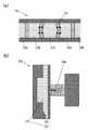
最初に、図5(a)に示すように、図2(a)〜(e)の工程で準備した樹脂フィルム12〜15を積層して、付着防止フィルム51、緩衝材52、金属板53を介して、ヒータ55が埋設された一対の熱プレス板54の間に挿入する。付着防止フィルム51は、加熱・加圧時の樹脂フィルム1が周りの部材へ付着したり、吸収層3が形成された樹脂フィルム1とインクパターン2iに傷がついたりするのを防止するもので、例えばポリイミドフィルム等が用いられる。緩衝材52は、樹脂フィルム12〜13を均等に加圧するためのもので、例えばステンレス等の金属を繊維状に裁断し、その繊維状金属を厚さ約1mmの板状に成型したものが用いられる。金属板53は、熱プレス板54に傷が入るのを防止するためのもので、例えばステンレス(SUS)やチタン(Ti)の厚さ約2mmの板が用いられる。
【0068】
次に図5(b)に示すように、最初にヒータ55を発熱し、圧力を印加しない状態で全体を150℃以下で5分間加熱する。次に、図示しないプレス機により熱プレス板54を介して、積層体に20kg/cm2の圧力を印加する。次に、全体の温度を200〜250℃に設定し、10〜30分間、加熱・加圧する。加熱・加圧は大気中で行なってもよいが、インクパターン2iや導電ペースト7p中に含まれる金属粒子の酸化を抑制するため、好ましくは真空中で行なうのがよい。
【0069】
以上の加熱・加圧により、樹脂フィルム12〜15の熱可塑性樹脂1が互いに接着する。尚、図5(a)に示すように、吸収層3はインクパターン2iの形成位置を含んで、各樹脂フィルム12〜15に部分的に形成されるため、積層される各樹脂フィルム12〜15の表面には、吸収層3が形成されない領域が存在する。従って、このような領域では、中間に吸収層3を介することなく、熱可塑性樹脂からなる樹脂フィルム1同士が直接貼り合わされる。これによって、樹脂フィルム1同士の貼り合わせ強度が増大し、図5(b)および図1に示す多層回路基板100の剥がれの発生が抑制される。
【0070】
また、加熱・加圧による樹脂フィルム12〜15の接着と同時に、インクパターン2iに含まれるナノメータオーダの顔料と導電ペースト7p中に含まれる金属粒子が焼結する。このインクパターン2iに含まれる金属粒子の焼結過程について、図6(a),(b)を用いて詳細に説明する。
【0071】
図6(a)は、焼結開始前のインクパターン2iに含まれるインクの顔料の模式図である。この焼結過程においては、加熱により図6(a)に示すように分散剤22が捕捉剤23に捕捉され、顔料21の表面から分散剤22が除去されて、顔料21の活性な表面が露出する。
【0072】
図6(b)は、焼結開始後のインクパターン2iに含まれるインクの顔料の模式図である。分散剤22が除去されてナノメータオーダの顔料21の活性な表面が露出すると、図6(b)に示すように、互いの顔料21の表面同士が接触して、界面での物質移動すなわち焼結が起こり、回路素材からなるインクの顔料が焼結されてなる膜21fが形成される。例えば、顔料21として粒径が50nm以下のAg粒子を用いる場合には、200℃程度でAg粒子が焼結し、Ag膜21fが形成されて図5(b)に示す回路パターン2となる。
【0073】
このように、粒径が50nm以下の金属粒子は、低い温度で焼結させることができる。このため、インクジェットによって形成された金属粒子からなるインクパターン2iの焼結を、樹脂フィルム1同士の貼り合わせおよび導電ペースト7pの焼結と同時に行なうことができる。従って、これにより製造工程が簡略化され、製造コストを低減することができる。
【0074】
以上のようにして、図5(b)に示すように、図5(a)の樹脂フィルム12〜15の各熱可塑性樹脂1が接着して一体化して絶縁材1となり、図5(a)の各インクパターン2iが焼結して回路パターン2が形成され、導電ペースト7pが焼結して接続導体7が形成される。
【0075】
このようにして、図1に示す微細で高精度な回路パターン2が形成され、剥がれの発生が抑制された多層回路基板100が製造される。上記した多層回路基板100の製造方法においては、加熱・加圧により、樹脂フィルム12〜15が一括して接着され、同時に導電ペースト7pとインクパターン2iが焼結して配線回路が形成される。このような同時形成により製造工程が簡略化されるため、多層回路基板100の製造コストを低減することができる。
【0076】
(他の実施形態)
図3(a)では、ナノメータオーダの顔料21として銀(Ag)を用いる例を示した。これによれば、図1に示す多層回路基板100においては、Agからなる回路パターン2が形成される。インク20に含まれるナノメータオーダの顔料21としては、Agに限らず、例えば金(Au)、白金(Pt)、スズ(Sn)の金属粒子を用いることができる。
【0077】
また、インク20に含まれる顔料21は、単一組成の金属粒子には限られない。インク20に含まれる顔料21の組成を変更して、例えば50nm以下のAg粒子と50nm以下のパラジウム(Pd)粒子の混合組成を用いれば、前記と同様の加熱・加圧による焼結時にAgとPdが合金化して、抵抗膜を形成することができる。従って、例えば、Ag粒子のみのインクで形成したインクパターンに連結して、Ag粒子とPd粒子を含むインクでインクパターンを形成すれば、前記と同様の製造方法を用いて、抵抗素子パターンを含む回路パターンを有した多層回路基板を製造することができる。また、多層回路基板に形成される回路パターンは、ナノメータオーダの誘電材料粒子を顔料とする容量素子であってもよい。
【0078】
このように、金属や誘電体の回路素材からなる粒径がナノメータオーダの微粒子を顔料として用い、インクジェットにより配線パターン、抵抗素子および容量素子といった各種の回路パターンを形成することができる。
【0079】
図5(a),(b)では、図2(a)〜(e)の工程で準備した,吸収層3上にインクパターン2iが形成された樹脂フィルム12〜15を積層して、多層回路基板100を形成する例を示した。積層される樹脂フィルムは、全てが図2(a)〜(e)の工程による、吸収層3上にインクパターン2iが形成された樹脂フィルムでなくともよい。例えば、従来の銅箔による回路パターンを形成した樹脂フィルムに、図2(a)〜(e)の工程で準備した吸収層3上にインクパターン2iが形成された樹脂フィルムを必要個所だけ積層し、多層回路基板を形成してもよい。
【図面の簡単な説明】
【図1】本発明の多層回路基板の断面図である。
【図2】(a)〜(e)は、本発明の多層回路基板の製造方法における、樹脂フィルムの準備工程を示す工程別断面図である。
【図3】(a)は、インクパターンの形成に用いるインクの模式図であり、(b)は、インクジェット装置によるインクパターンの形成の様子を示す模式図である。
【図4】(a),(b)は、ピエゾ素子を用いた他の吐出方式のインクジェット装置を説明する図である。
【図5】(a),(b)は、本発明の多層回路基板の製造方法における、樹脂フィルムの貼り合わせの様子を示す工程別断面図である。
【図6】(a)は、焼結開始前のインクパターンに含まれるインクの顔料の模式図であり、(b)は、焼結開始後のインクパターンに含まれるインクの顔料の模式図である。
【符号の説明】
100 多層回路基板
1 絶縁母材(樹脂フィルム)
2 回路パターン
2i インクパターン
3 吸収層
6 貫通孔
7 接続導体
7p 導電ペースト
11〜15 吸収層上にインクパターンが形成された樹脂フィルム
20,20a〜20e インク
21 ナノメータオーダのインクの顔料
22 分散剤
23 捕捉剤
24 溶媒
30,30r,30s インクジェット装置[0001]
BACKGROUND OF THE INVENTION
The present invention relates to a multilayer circuit board formed with an ink-jet circuit pattern and a method for manufacturing the same.
[0002]
[Prior art]
A multilayer circuit board formed by laminating a plurality of resin films on which a circuit pattern is formed and a method for manufacturing the same are disclosed in, for example, Japanese Unexamined Patent Publication No. 2000-38464 (Patent Document 1).
[0003]
According to the method for manufacturing a multilayer circuit board disclosed in
[0004]
On the other hand, an electronic device using ink jet and a method for manufacturing the same are disclosed in Japanese Patent Laid-Open No. 11-274681 (Patent Document 2).
[0005]
According to the electronic device disclosed in
[0006]
[Patent Document 1] JP 2000-38464 A
[0007]
[Patent Document 2] JP-A-11-274681
[0008]
[Problems to be solved by the invention]
According to the method for manufacturing a multilayer circuit board disclosed in
[0009]
In order to solve this problem, the inventors have not formed a circuit pattern from a thick copper foil, but a method of manufacturing a multilayer circuit board using the formation of a circuit pattern by inkjet, and the multilayer circuit board manufactured thereby Was invented. According to this, the circuit pattern forming process in the manufacturing process of the multilayer circuit board is simplified, and the miniaturization of the circuit pattern can be promoted. A patent application has already been filed for this invention (application number 2002-31650).
[0010]
Circuit pattern formation by inkjet is a method of forming a circuit pattern by ejecting ink in the form of droplets and landing on the substrate surface. In order to improve the accuracy of the circuit pattern of the multilayer circuit board by using this ink jet and further promote the miniaturization, the spread due to the impact when the ink droplets land and the spread due to the bleeding due to the surface state of the substrate Need to prevent. Further, the dimensional accuracy of the circuit pattern also deteriorates when adjacent ink droplets are combined to form a large droplet.
[0011]
On the other hand, according to the electronic device and the manufacturing method thereof disclosed in
[0012]
Accordingly, an object of the present invention is to prevent the spread and combination of ink droplets when forming a circuit pattern by ink jet, to form a fine and highly accurate circuit pattern, and to prevent the occurrence of peeling, and a method for manufacturing the same Is to provide.
[0013]
[Means for Solving the Problems]
The invention described in
[0014]
According to this, the absorption layer laminated on the resin film quickly absorbs the solvent of the ink, thereby preventing spread due to ink droplet bleeding due to the surface state of the resin film. In addition, after the ink droplets have landed, the ink solvent is immediately absorbed by the absorption layer, so that even if the ink droplets land adjacently, the ink droplets are combined to deteriorate the dimensional accuracy of the circuit pattern. There is nothing. In this way, the multilayer circuit board of the present invention can prevent the ink droplets from spreading and bonding when forming a circuit pattern by inkjet, and can be a multilayer circuit board on which a fine and highly accurate circuit pattern is formed.
[0015]
Moreover, since the absorption layer is partially formed on the resin film, there is a region where the absorption layer is not formed on the surface of the resin film. In a multilayer circuit board in which such resin films are laminated, there is a region where resin films made of a thermoplastic resin are directly bonded to each other without interposing an absorption layer therebetween. Thereby, the bonding strength between the resin films is increased, and a multilayer circuit board in which the occurrence of peeling is suppressed can be obtained.
[0016]
The invention described in
[0017]
Metal particles having a particle size of 50 nm or less can be sintered at a low temperature. For this reason, the pattern which consists of the metal particle formed by the inkjet can be performed simultaneously with the bonding of the resin films and the sintering of the conductive paste. Therefore, the manufacturing process is simplified and an inexpensive multilayer circuit board can be obtained.
[0018]
According to a third aspect of the present invention, the pigment has a particle size of 5 nm or more, the absorption layer is a fine particle layer in which fine particles made of either aluminum oxide or silicon oxide are dispersed, and the fine particle layer has voids. It is characterized by being 5 nm or less.
[0019]
Aluminum oxide or silicon oxide can be made into fine particles having a particle size on the order of nanometers, and the voids can be made 5 nm or less in the fine particle layer in which the fine particles of nanometer order are dispersed. By using such a fine particle layer as an absorption layer and setting the particle size of the ink pigment to 5 nm or more, the pigment contained in the ink droplets that have landed on the absorption layer can penetrate into the absorption layer together with the solvent. Disappears. In other words, only the ink solvent is absorbed by the absorption layer, and the pigment remains on the surface of the absorption layer. Thereby, it can prevent that a pigment penetrate | invades into the inside of an absorption layer, the defect | deletion of a circuit pattern generate | occur | produces, or short circuit failure generate | occur | produces.
[0020]
The invention according to claim 4 is characterized in that the absorption layer is a swelling layer made of either urethane resin or acrylic resin having swelling property.
[0021]
Urethane resins or acrylic resins have resistance and swelling to general ink solvents and also have heat resistance to heat treatment. If an absorbing layer is formed using this urethane resin or acrylic resin, the swelling layer absorbs only the solvent contained in the ink droplets that have landed on the absorbing layer due to the swelling property of the ink with respect to the solvent, and the ink pigment is the absorbing layer. It can be left on the surface. Thereby, it can prevent that a pigment penetrate | invades into the inside of an absorption layer, the defect | deletion of a circuit pattern generate | occur | produces, or short circuit failure generate | occur | produces.
[0022]
The invention described in claims 5 to 10 relates to a method of manufacturing the multilayer circuit board.
[0023]
According to a fifth aspect of the present invention, there is provided a method for manufacturing a multilayer circuit board in which a plurality of resin films made of a thermoplastic resin having a circuit pattern formed by inkjet are laminated, and the ink solvent is absorbed on the resin film. An absorption layer forming step of partially forming the absorption layer including a position where the circuit pattern is formed, a through hole forming step of forming a through hole in the resin film on which the absorption layer is formed, The conductive paste filling step of filling the through hole with the conductive paste and the ink containing the pigment made of the circuit material having a particle size of nanometer order are ejected onto the absorption layer by the ink jet apparatus, and the formation position of the through hole is included. In the ink pattern forming step of forming a circuit pattern with the ink on the surface of the absorption layer, the conductive paste is filled in the through-hole, A laminating step of laminating a plurality of resin films having a pattern formed on the absorbent layer, and heating and pressurizing the laminated resin films with a hot press plate to bond the resin films to each other, It has a heating and pressing step of sintering the conductive paste and the ink pattern.
[0024]
By using this multilayer circuit board manufacturing method, a multilayer circuit board in which the above-described fine and highly accurate circuit pattern is formed and peeling is suppressed can be manufactured. In this method of manufacturing a multilayer circuit board, the resin film is bonded together by heating and pressing, and at the same time, the conductive paste and the ink pattern are sintered to form a wiring circuit. The manufacturing cost of the substrate can be reduced.
[0025]
The inventions described in
[0026]
The invention according to claim 8 is characterized in that the absorption layer is formed by discharging an ink containing a pigment composed of the fine particles onto a resin film by an ink jet apparatus.
[0027]
Thereby, an absorption layer can be partially formed on a resin film using the same inkjet apparatus as the formation of an ink pattern. Therefore, the manufacturing cost can be reduced by using the same apparatus.
[0028]
The invention described in
[0029]
The invention according to claim 10 is characterized in that the absorption layer is formed by ejecting an ink containing a dye made of a resin of the swelling layer onto a resin film by an ink jet apparatus.
[0030]
Thereby, an absorption layer can be partially formed on a resin film using the same inkjet apparatus as formation of a circuit pattern. Therefore, the manufacturing cost can be reduced by using the same apparatus.
[0031]
DETAILED DESCRIPTION OF THE INVENTION
Hereinafter, a multilayer circuit board and a manufacturing method thereof according to the present invention will be described with reference to the drawings.
[0032]
FIG. 1 is a cross-sectional view of a
[0033]
In the
[0034]
In the
[0035]
In the
[0036]
As the
[0037]
In the
[0038]
Therefore, by forming the
[0039]
The thickness of the
[0040]
In the
[0041]
Next, a method for manufacturing the
[0042]
2 (a) to 2 (e) are cross-sectional views showing process steps for preparing a resin film in the method for manufacturing a multilayer circuit board according to the present invention.
[0043]
First, as shown in FIG. 2A, a
[0044]
Next, the
[0045]
As described above, the absorbing
[0046]
In order to partially form the
[0047]
Next, as shown in FIG.2 (b), the through-
[0048]
Next, as shown in FIG. 2 (c), the
[0049]
Next, as shown in FIG.2 (d), the
[0050]
Next, an ink pattern 2i is formed as shown in FIG. The formation of the ink pattern 2i will be described in detail with reference to FIGS. 3 (a) and 3 (b).
[0051]
FIG. 3A is a schematic diagram of the ink used for forming the ink pattern 2i of FIG. The
[0052]
As the nanometer-
[0053]
Further, as the
[0054]
Next, as the
[0055]
FIG. 3B is a schematic diagram illustrating how the ink pattern 2 i is formed by the
[0056]
The
[0057]
In addition to the method shown in FIG. 3B, the ink jet method for ejecting liquid droplets using a piezo element includes the method shown in FIGS. 4A and 4B.
[0058]
In the method of the
[0059]
In addition to the above-described method using a piezo element, a bubble jet (registered trademark) method or a thermal jet using a “film boiling phenomenon” generated by forming a heater in a pressure chamber and passing a current through the heater. There are also methods. In order to form the ink pattern 2i shown in FIG. 3B, it is possible to apply an ink jet apparatus of any ejection method that utilizes mechanical deformation or boiling phenomenon, including other ejection methods.
[0060]
In FIG. 3B, when the ejected ink droplet of several picoliters reaches the surface of the
[0061]
In addition, as described above, the
[0062]
In this way, the drawn ink pattern 2i can be a fine and highly accurate ink pattern 2i that is prevented from spreading and combining ink droplets and that is free from defects and short-circuit defects.
[0063]
In FIG. 2A, printing or transfer is taken as an example of a method for partially applying the
[0064]
As described above, the
[0065]
Next, a multilayer circuit board is manufactured by laminating a plurality of resin films having the conductive paste and ink pattern prepared as described above and bonding them by heating and pressing.
[0066]
5 (a) and 5 (b) are cross-sectional views by process showing the state of bonding of resin films in the method for producing a multilayer circuit board of the present invention.
[0067]
First, as shown in FIG. 5A, the
[0068]
Next, as shown in FIG. 5B, the
[0069]
The
[0070]
Simultaneously with the adhesion of the
[0071]
FIG. 6A is a schematic diagram of ink pigments included in the ink pattern 2i before the start of sintering. In this sintering process, as shown in FIG. 6 (a), the
[0072]
FIG. 6B is a schematic diagram of ink pigments included in the ink pattern 2i after the start of sintering. When the dispersing
[0073]
Thus, metal particles having a particle size of 50 nm or less can be sintered at a low temperature. For this reason, sintering of the ink pattern 2i made of metal particles formed by inkjet can be performed simultaneously with the bonding of the
[0074]
As described above, as shown in FIG. 5B, the
[0075]
In this way, the
[0076]
(Other embodiments)
FIG. 3A shows an example in which silver (Ag) is used as the nanometer-
[0077]
Further, the
[0078]
As described above, various circuit patterns such as a wiring pattern, a resistance element, and a capacitance element can be formed by inkjet using fine particles having a particle size of nanometer order made of a metal or dielectric circuit material as a pigment.
[0079]
5 (a) and 5 (b), the
[Brief description of the drawings]
FIG. 1 is a cross-sectional view of a multilayer circuit board according to the present invention.
FIGS. 2A to 2E are cross-sectional views showing process steps for preparing a resin film in the method for producing a multilayer circuit board according to the present invention. FIGS.
FIG. 3A is a schematic diagram of ink used for forming an ink pattern, and FIG. 3B is a schematic diagram illustrating how an ink pattern is formed by an inkjet apparatus.
FIGS. 4A and 4B are diagrams illustrating an ink jet apparatus of another ejection method using a piezo element. FIGS.
FIGS. 5A and 5B are cross-sectional views showing a state of bonding of resin films in the method for manufacturing a multilayer circuit board according to the present invention.
6A is a schematic diagram of ink pigments included in an ink pattern before the start of sintering, and FIG. 6B is a schematic diagram of ink pigments included in the ink pattern after the start of sintering. is there.
[Explanation of symbols]
100 multilayer circuit board
1 Insulation base material (resin film)
2 Circuit pattern
2i ink pattern
3 Absorption layer
6 Through hole
7 Connecting conductor
7p conductive paste
11-15 Resin film having an ink pattern formed on the absorbent layer
20, 20a-20e ink
21 Ink pigment of nanometer order
22 Dispersant
23 Scavenger
24 Solvent
30, 30r, 30s inkjet device
Claims (10)
Translated fromJapanese絶縁母材となる相互に貼り合わされた複数枚の樹脂フィルムと、
当該各樹脂フィルム上に、回路パターンが形成される位置を含んで部分的に形成されてなる、インクの溶媒を吸収する吸収層と、
当該吸収層上に形成され、粒径がナノメータオーダの回路素材からなるインクの顔料が焼結されてなる回路パターンと、
前記樹脂フィルムと吸収層を貫通する貫通孔に充填された導電ペーストが焼結されてなり、前記回路パターン同士を接続する接続導体とを有することを特徴とする多層回路基板。A multilayer circuit board formed by laminating a plurality of resin films made of a thermoplastic resin on which a circuit pattern by inkjet is formed,
A plurality of resin films bonded to each other as an insulating base material;
An absorbing layer that absorbs the solvent of the ink, which is partially formed on each resin film including the position where the circuit pattern is formed,
A circuit pattern formed on the absorbing layer and sintered with an ink pigment made of a circuit material having a particle size of the order of nanometers;
A multilayer circuit board, comprising: a conductive paste filled in a through-hole penetrating the resin film and an absorption layer; and a connection conductor connecting the circuit patterns.
樹脂フィルム上に、インクの溶媒を吸収する吸収層を、回路パターンが形成される位置を含んで、部分的に形成する吸収層形成工程と、
前記吸収層が形成された樹脂フィルムに、貫通孔を形成する貫通孔形成工程と、
前記貫通孔に、導電ペーストを充填する導電ペースト充填工程と、
インクジェット装置により、粒径がナノメータオーダの回路素材からなる顔料を含むインクを前記吸収層上に吐出し、前記貫通孔の形成位置を含んで、吸収層の表面に当該インクによる回路パターンを形成するインクパターン形成工程と、
前記導電ペーストが貫通孔に充填され、前記インクパターンが吸収層上に形成された複数枚の樹脂フィルムを積層する積層工程と、
前記積層された樹脂フィルムを、熱プレス板により加熱・加圧して、樹脂フィルムを相互に貼り合わせると共に、前記導電ペーストとインクパターンを焼結する加熱加圧工程とを有することを特徴とする多層回路基板の製造方法。In a method for manufacturing a multilayer circuit board in which a plurality of resin films made of a thermoplastic resin having a circuit pattern formed by inkjet are laminated,
An absorption layer forming step of partially forming an absorption layer that absorbs the solvent of the ink on the resin film, including the position where the circuit pattern is formed;
A through hole forming step of forming a through hole in the resin film on which the absorption layer is formed;
A conductive paste filling step of filling the through hole with a conductive paste;
An ink containing a pigment made of a circuit material having a particle size of the order of nanometers is ejected onto the absorption layer by an inkjet device, and a circuit pattern is formed on the surface of the absorption layer including the formation position of the through hole An ink pattern forming step;
A laminating step of laminating a plurality of resin films in which the conductive paste is filled in through holes and the ink pattern is formed on an absorption layer;
The multilayer resin film has a heating and pressurizing step of heating and pressing the laminated resin film with a hot press plate to bond the resin films to each other and sintering the conductive paste and the ink pattern. A method of manufacturing a circuit board.
Priority Applications (1)
| Application Number | Priority Date | Filing Date | Title |
|---|---|---|---|
| JP2002375231AJP4212887B2 (en) | 2002-12-25 | 2002-12-25 | Multilayer circuit board manufacturing method |
Applications Claiming Priority (1)
| Application Number | Priority Date | Filing Date | Title |
|---|---|---|---|
| JP2002375231AJP4212887B2 (en) | 2002-12-25 | 2002-12-25 | Multilayer circuit board manufacturing method |
Publications (2)
| Publication Number | Publication Date |
|---|---|
| JP2004207510Atrue JP2004207510A (en) | 2004-07-22 |
| JP4212887B2 JP4212887B2 (en) | 2009-01-21 |
Family
ID=32813037
Family Applications (1)
| Application Number | Title | Priority Date | Filing Date |
|---|---|---|---|
| JP2002375231AExpired - Fee RelatedJP4212887B2 (en) | 2002-12-25 | 2002-12-25 | Multilayer circuit board manufacturing method |
Country Status (1)
| Country | Link |
|---|---|
| JP (1) | JP4212887B2 (en) |
Cited By (7)
| Publication number | Priority date | Publication date | Assignee | Title |
|---|---|---|---|---|
| KR100657410B1 (en) | 2006-02-15 | 2006-12-14 | 삼성전기주식회사 | Manufacturing multi-layer pcb |
| KR100657409B1 (en) | 2006-02-15 | 2006-12-14 | 삼성전기주식회사 | Multi-layer printed circuit board manufacturing method |
| JP2007139995A (en)* | 2005-11-17 | 2007-06-07 | Hitachi Displays Ltd | Display device and manufacturing method thereof |
| KR100865120B1 (en) | 2006-07-31 | 2008-10-24 | 한국생산기술연구원 | Manufacturing method of multilayer printed circuit board using inkjet printing method |
| JP2009206225A (en)* | 2008-02-27 | 2009-09-10 | Panasonic Corp | Method of manufacturing circuit board |
| JP2010118589A (en)* | 2008-11-14 | 2010-05-27 | Shinko Electric Ind Co Ltd | Method of manufacturing wiring board with electronic component incorporated therein |
| JP2016213325A (en)* | 2015-05-08 | 2016-12-15 | 富士通株式会社 | Multilayer wiring structure, multilayer wiring board, and manufacturing method of multilayer wiring structure |
Families Citing this family (1)
| Publication number | Priority date | Publication date | Assignee | Title |
|---|---|---|---|---|
| JP2576831B2 (en) | 1994-04-18 | 1997-01-29 | 株式会社ジャパンエナジー | Process for producing dihalogenophosphonyl and monoalkylphosphine |
- 2002
- 2002-12-25JPJP2002375231Apatent/JP4212887B2/ennot_activeExpired - Fee Related
Cited By (7)
| Publication number | Priority date | Publication date | Assignee | Title |
|---|---|---|---|---|
| JP2007139995A (en)* | 2005-11-17 | 2007-06-07 | Hitachi Displays Ltd | Display device and manufacturing method thereof |
| KR100657410B1 (en) | 2006-02-15 | 2006-12-14 | 삼성전기주식회사 | Manufacturing multi-layer pcb |
| KR100657409B1 (en) | 2006-02-15 | 2006-12-14 | 삼성전기주식회사 | Multi-layer printed circuit board manufacturing method |
| KR100865120B1 (en) | 2006-07-31 | 2008-10-24 | 한국생산기술연구원 | Manufacturing method of multilayer printed circuit board using inkjet printing method |
| JP2009206225A (en)* | 2008-02-27 | 2009-09-10 | Panasonic Corp | Method of manufacturing circuit board |
| JP2010118589A (en)* | 2008-11-14 | 2010-05-27 | Shinko Electric Ind Co Ltd | Method of manufacturing wiring board with electronic component incorporated therein |
| JP2016213325A (en)* | 2015-05-08 | 2016-12-15 | 富士通株式会社 | Multilayer wiring structure, multilayer wiring board, and manufacturing method of multilayer wiring structure |
Also Published As
| Publication number | Publication date |
|---|---|
| JP4212887B2 (en) | 2009-01-21 |
Similar Documents
| Publication | Publication Date | Title |
|---|---|---|
| JP4192554B2 (en) | Multilayer circuit board manufacturing method | |
| JP5497347B2 (en) | Wiring board | |
| JP2004304129A (en) | Pattern forming method by droplet discharging method, forming method of multilayer wiring structure | |
| JP4212887B2 (en) | Multilayer circuit board manufacturing method | |
| WO2000035260A1 (en) | Method of manufacturing ceramic substrate | |
| JP4386161B2 (en) | Conductive film pattern and method for forming the same, wiring board, and electronic device | |
| JP2005057140A (en) | Multilayer wiring board and manufacturing method thereof | |
| JP4270900B2 (en) | Paste filling method and multilayer circuit board manufacturing method | |
| JP2005057139A (en) | Multilayer wiring board and manufacturing method thereof | |
| CN102137550A (en) | Method for producing build-up substrate | |
| JP2007084387A (en) | Manufacturing method of ceramic circuit board | |
| JP2009123731A (en) | Manufacturing method of ceramic multilayer substrate | |
| JP2019106400A (en) | Substrate for electronic device, electronic device, and manufacturing method of electronic device | |
| JP5103206B2 (en) | Manufacturing method of ceramic multilayer substrate | |
| JP2007088382A (en) | Film pattern and manufacturing method thereof | |
| KR20080048940A (en) | Pattern Forming Method, Droplet Discharge Device and Circuit Board | |
| JPH11102834A (en) | Aqueous ink for internal electrodes of multilayer ceramic capacitors | |
| JP3823457B2 (en) | Manufacturing method of ceramic wiring board | |
| JP4998274B2 (en) | Manufacturing method of ceramic multilayer substrate | |
| JP4953626B2 (en) | Manufacturing method of ceramic electronic component | |
| JP2008294244A (en) | Wiring pattern connection method, wiring sheet, and wiring sheet laminate | |
| JP7751871B2 (en) | Method for manufacturing a printed circuit board and method for forming a conductive base layer | |
| JP2009158847A (en) | Manufacturing method of ceramic multilayer substrate | |
| JP2004235400A (en) | Surface treatment layer for water-based ink and printing method using the same | |
| JP2009129986A (en) | Manufacturing method of ceramic multilayer substrate |
Legal Events
| Date | Code | Title | Description |
|---|---|---|---|
| A621 | Written request for application examination | Free format text:JAPANESE INTERMEDIATE CODE: A621 Effective date:20051214 | |
| A977 | Report on retrieval | Free format text:JAPANESE INTERMEDIATE CODE: A971007 Effective date:20080423 | |
| A131 | Notification of reasons for refusal | Free format text:JAPANESE INTERMEDIATE CODE: A131 Effective date:20080513 | |
| A521 | Request for written amendment filed | Free format text:JAPANESE INTERMEDIATE CODE: A523 Effective date:20080711 | |
| A521 | Request for written amendment filed | Free format text:JAPANESE INTERMEDIATE CODE: A523 Effective date:20080724 | |
| TRDD | Decision of grant or rejection written | ||
| A01 | Written decision to grant a patent or to grant a registration (utility model) | Free format text:JAPANESE INTERMEDIATE CODE: A01 Effective date:20081028 | |
| A01 | Written decision to grant a patent or to grant a registration (utility model) | Free format text:JAPANESE INTERMEDIATE CODE: A01 | |
| A61 | First payment of annual fees (during grant procedure) | Free format text:JAPANESE INTERMEDIATE CODE: A61 Effective date:20081029 | |
| FPAY | Renewal fee payment (event date is renewal date of database) | Free format text:PAYMENT UNTIL: 20111107 Year of fee payment:3 | |
| R150 | Certificate of patent or registration of utility model | Ref document number:4212887 Country of ref document:JP Free format text:JAPANESE INTERMEDIATE CODE: R150 Free format text:JAPANESE INTERMEDIATE CODE: R150 | |
| FPAY | Renewal fee payment (event date is renewal date of database) | Free format text:PAYMENT UNTIL: 20111107 Year of fee payment:3 | |
| FPAY | Renewal fee payment (event date is renewal date of database) | Free format text:PAYMENT UNTIL: 20121107 Year of fee payment:4 | |
| FPAY | Renewal fee payment (event date is renewal date of database) | Free format text:PAYMENT UNTIL: 20131107 Year of fee payment:5 | |
| R250 | Receipt of annual fees | Free format text:JAPANESE INTERMEDIATE CODE: R250 | |
| R250 | Receipt of annual fees | Free format text:JAPANESE INTERMEDIATE CODE: R250 | |
| R250 | Receipt of annual fees | Free format text:JAPANESE INTERMEDIATE CODE: R250 | |
| R250 | Receipt of annual fees | Free format text:JAPANESE INTERMEDIATE CODE: R250 | |
| R250 | Receipt of annual fees | Free format text:JAPANESE INTERMEDIATE CODE: R250 | |
| R250 | Receipt of annual fees | Free format text:JAPANESE INTERMEDIATE CODE: R250 | |
| R250 | Receipt of annual fees | Free format text:JAPANESE INTERMEDIATE CODE: R250 | |
| LAPS | Cancellation because of no payment of annual fees |