JP2004206245A - Non-contact IC card reading / writing device - Google Patents
Non-contact IC card reading / writing deviceDownload PDFInfo
- Publication number
- JP2004206245A JP2004206245AJP2002372222AJP2002372222AJP2004206245AJP 2004206245 AJP2004206245 AJP 2004206245AJP 2002372222 AJP2002372222 AJP 2002372222AJP 2002372222 AJP2002372222 AJP 2002372222AJP 2004206245 AJP2004206245 AJP 2004206245A
- Authority
- JP
- Japan
- Prior art keywords
- contact
- card
- loop antenna
- unit
- wireless
- Prior art date
- Legal status (The legal status is an assumption and is not a legal conclusion. Google has not performed a legal analysis and makes no representation as to the accuracy of the status listed.)
- Pending
Links
Images


Landscapes
- Near-Field Transmission Systems (AREA)
Abstract
Translated fromJapaneseDescription
Translated fromJapanese【0001】
【発明の属する技術分野】
本発明は非接触ICカードシステムで用いられる読取/書込装置に係り、特に非接触ICカードへの電力伝送効率、および非接触ICカードからのデータ受信効率を改良した非接触ICカード読取/書込装置に関するものである。
【0002】
【従来の技術】
従来、ICカードを用いた読取/書込システムは、一般に非接触ICカードシステムと呼ばれ、例えば13.56MHzの周波数帯を利用した物流システム、交通システム、航空貨物管理システム等々に実用化されつつある。
【0003】
ここで、図4は従来の非接触ICカードシステムの説明概念図である。このシステムは、図4に示すように、1枚の樹脂製カード上にICチップ103とアンテナコイル102を備えた非接触ICカード101(以下、略してICカードと言うこともある。)と、このICカードとの通信を行う読取/書込装置105とを備え、この読取/書込装置105にはループアンテナ104が備えられている。このループアンテナ104により電力と送信データを常時または間欠に送信し、この電力と送信データを受信できる範囲内にあるICカードからの受信データを得るものである。
【0004】
一例として(特許文献1)に記載の非接触ICカードシステムの読取/書込装置を図5に示す。図5は、従来の非接触ICカード読取/書込装置のブロック図であり、上記した従来の非接触ICカードシステムの、読取/書込装置と非接触ICカードの結合に関連する部分を示している。
【0005】
まず、送信データ伝送の場合は、発振器106からの搬送波を変調器107へ入力し、データDATAaによりこれを変調する。そしてこれを電力増幅器108で増幅し、マッチング回路109を介してループアンテナ110から送信する。
【0006】
また、電力伝送のみの場合は、発振器106からの搬送波を無変調のままで送信する。この読取/書込装置111から非接触ICカード112への送信は、電磁結合によりループアンテナ110が生成する磁束が非接触ICカード112のアンテナコイル102と鎖交し、誘起電圧を励起することにより行われる。非接触ICカード112側では、アンテナコイル102の誘起電圧をICチップ103内の整流回路(図示せず)で整流し、非接触ICカード112内の各回路の電源として用いる。また、同じ誘起電圧を復調回路(図示せず)へ導いて読取/書込装置からのデータを復調する。
【0007】
次に、非接触ICカード112より読取/書込装置111へのデータ伝送時には、読取/書込装置111は無変調の搬送波を送信して、非接触ICカード112へ電力供給のみを行っている。非接触ICカード112側では、ICチップ103内のメモリ(図示せず)から読み出されたデータDATAbに応じて、例えばアンテナコイル102に接続された負荷抵抗(図示せず)とスイッチ(図示せず)とからなる変調回路(図示せず)にて、データの“1”、“0”ビットに応じて、このスイッチがオン、オフされる。上記のようにスイッチがオン、オフすると、アンテナコイル102に対する負荷が変動し、この変動が読取/書込装置側のループアンテナ110へ電磁誘導により伝わり、ループアンテナ110側のインピーダンスが変動し、読取/書込装置111の点Aに於ける電圧/電流すなわちインピーダンスが、非接触ICカード112の送信データDATAbに応じて変化する。結果として高周波信号の振幅が変動する。即ち、この高周波信号は非接触ICカード112のデータによって振幅変調される。この変調高周波信号が復調回路114で復調されてデータDATAbが得られる。
【0008】
【特許文献1】
特開2002−007976号公報
【0009】
【発明が解決しようとする課題】
第一の従来例を図5(b)に示す。図5(b)は、図5(a)に於ける復調回路114の入力部分の詳細図である。前述のように非接触ICカード112からデータを送るときは、非接触ICカード112のアンテナコイル102の負荷ZがデータDATAbにより変化し、これによって電力増幅器108の出力電流Iが変化する。そこでこの変化を検出するために、ループアンテナ110の接地側に抵抗器115を挿入し、ここを電流Iが流れることにより生じる電圧降下を復調回路114へ入力する。復調回路114は、入力された電圧の変化を検出して非接触ICカード112からのDATAbを復調する。ところが、抵抗器115に電力増幅器108からの電流Iを流すと、ここで電力が消費される。このために電力増幅器108は、この抵抗器115で消費される分だけ余計な出力電力を必要とし、電力伝送効率が低下する。
【0010】
ここで、図6は従来の非接触ICカード読取/書込装置のブロック図である。第二の従来例として図6(a)は並列共振を用いたときの復調回路の周辺を詳細に示したもので、コンデンサ116がループアンテナ110と並列共振する。この場合、並列共振回路のインピーダンスはその共振点付近では大きな値となるから、マッチング回路109の出力側インピーダンスもそれに合わせて大きな値であり、このハイインピーダンス点の電圧Vを抵抗器117を介して復調回路114へ取り込み復調することとなる。この構成では、搬送波電流は抵抗器117と復調回路114の搬送波帯での入力インピーダンスとの直列インピーダンスが、ループアンテナ110とコンデンサ116からなる並列回路に並列に入ることになり、非接触ICカード112からのデータ検出のために共振回路のQを低下させることとなってしまう。これは直ちに非接触ICカード112への電力伝送効率を低下させる。
【0011】
また、図6(b)は、第三の従来例として、直列共振によって電力伝送効率を向上させた場合の、復調回路114の周辺を示したもので、この場合にはループアンテナ110とコンデンサ118とからなる直列共振回路を形成している。直列共振時にはその回路のインピーダンスは小さい値となるので、この場合は電力増幅器108からの電流Iを抵抗器119へ流し、その電圧降下を復調回路114で検出する。従って、抵抗器119に於ける電力消費が生じ、さらにこの場合には直列共振回路に抵抗器119が直列に入ることになってQが低下し、電力伝送効率を低下させる。
【0012】
さらに、図6(c)は、第四の従来例として、復調回路入力部およびその周辺の回路構成を示したもので、巻線n1、n2、n3を有したマッチングトランス120により、電力増幅器108と並列共振回路121、及び復調回路114が結合された構成である。ここで、巻線n1と巻線n2の巻数比は、電力増幅器108の出力と並列共振回路121との間で、並列共振回路121の共振周波数での整合をとる値に設定される。復調回路114との結合もこのマッチングトランス120で行うようにしている。そして、巻線n3と巻線n2の巻数比は、非接触ICカードからのデータDATAbの周波数帯域で整合がとれるように構成されている。しかしながら、この構成ではマッチングトランス120の挿入損が生じ電力伝送効率を低下させてしまう。
【0013】
さらに、第一から第四の従来例のいずれの回路においても、電力、送信データおよび受信データの伝送方向の方向性がなく、従来例のいずれの場合も電力増幅器108からの出力はループアンテナ110と復調回路114のいずれへも供給され、これによりループアンテナ110からの空間への放射電力が、復調回路110側へ流れた分だけ電力損失となり電力伝送効率が低下する。
【0014】
また受信データを取得する場合もループアンテナ110での負荷インピーダンスの変化が復調回路114と電力増幅器108のいずれの側へも伝わり、これによりループアンテナ110からの負荷インピーダンスの変化が復調回路114側で低下する。
【0015】
さらに電力増幅器108からの大振幅の高周波信号が復調回路114へ流入する事により、この大振幅の高周波信号をフィルタリングする為に、高性能な帯域阻止特性を有するフィルタ回路を復調回路114の前段に設けねばならないという課題があった。
【0016】
そこで、本発明は上記従来の課題を解決するものであり、良好な受信特性を有する非接触ICカード読取/書込装置を提供する事を目的とする。
【0017】
【課題を解決するための手段】
本発明は、非接触ICカードに電磁誘導により電力と送信信号を供給し、非接触ICカードから受信信号を負荷変動により取得するループアンテナと、このループアンテナを所望の周波数に共振させるための共振回路部と、共振回路部を介しループアンテナに電力と送信データを供給する無線送信部および、ループアンテナから共振回路部を介して受信信号を取得する無線受信部を設け、その受信信号から復調回路により非接触ICカードからのデータを復調するように構成され、共振回路部と無線送信部と無線受信部を、方向性結合器、サーキュレータ、アイソレータのいずれか1つを介し結合した構成としたものである。
【0018】
【発明の実施の形態】
本発明の請求項1に記載の発明は、非接触ICカードに電磁誘導により電力と送信信号を供給し、非接触ICカードから受信信号を負荷変動により取得するループアンテナと、このループアンテナを所望の周波数に共振させるための共振回路部と、共振回路部を介しループアンテナに電力と送信データを供給する無線送信部および、ループアンテナから共振回路部を介して受信信号を取得する無線受信部を設け、その受信信号から復調回路により非接触ICカードからのデータを復調するように構成された非接触ICカード読取/書込装置であり、共振回路部と無線送信部と無線受信部を方向性結合器で結合した構成のものである。
【0019】
無線送信部と、ループアンテナとコンデンサから成る共振回路部の間に、方向性結合器の一次線路を、ループアンテナとコンデンサから成る共振回路部と、無線受信部との間に方向性結合器の二次線路を挿入した事により、無線送信部、無線受信部間にアイソレーションを、またループアンテナとコンデンサから成る共振回路部と無線受信部間に方向性をもたすことができる。
【0020】
その結果、無線送信部、無線受信部間にアイソレーションをもたすことにより、無線送信部からの大振幅の高周波信号が、無線受信部内の復調回路へ流入する事を大幅に低減することが出来る。それゆえ従来この大振幅の高周波信号をフィルタリングする為に必要であった復調回路前段の高性能な帯域阻止特性を有するフィルタ回路が不要となり、且つフィルタ回路の挿入損失分の効率低下を受けなくなる。
【0021】
さらに、ループアンテナとコンデンサから成る共振回路部と無線受信部間に方向性をもたすことにより、ループアンテナ側から無線受信部側へ流れる高周波信号、すなわち無線送信部から発した高周波信号(入射波)が方向性結合器の一次線路を経由して、ループアンテナ側へ到達し、所望の周波数帯でのアンテナインピーダンスに応じた反射波としてループアンテナ側より反射され、波の進行方向が逆方向の高周波信号(反射波)として、再び方向性結合器に入力され、方向性結合器の二次線路の一端より出力され無線受信部へと導かれる。その結果、無線受信部への入力信号は、上記のように所望の周波数帯でのアンテナインピーダンスに応じた高周波信号(反射波)のみとなり、理想的な回路構成となり、良好な受信特性を有する読取/書込装置が提供可能となる。
【0022】
また、請求項2に記載の発明は、共振回路部と無線送信部と無線受信部をサーキュレータで結合した構成である。
【0023】
無線送信部と、ループアンテナとコンデンサから成る共振回路部の間にサーキュレータの一次線路を、ループアンテナとコンデンサから成る共振回路部と、無線受信部との間にサーキュレータの二次線路を挿入した事により、無線送信部、無線受信部間にアイソレーションを、またループアンテナとコンデンサから成る共振回路部と、無線受信部間に方向性をもたすことができる。
【0024】
その結果、無線送信部、無線受信部間にアイソレーションをもたすことにより、無線送信部からの大振幅の高周波信号が、無線受信部内の復調回路へ流入する事を大幅に低減することが出来る。それゆえ従来この大振幅の高周波信号をフィルタリングする為に必要であった復調回路前段の高性能な帯域阻止特性を有するフィルタ回路が不要となり、且つフィルタ回路の挿入損失分の効率低下を受けなくなる。
【0025】
さらに、ループアンテナとコンデンサから成る共振回路部と、無線受信部間に方向性をもたすことにより、ループアンテナ側から無線受信部側へ流れる高周波信号、すなわち無線送信部から発した高周波信号(入射波)がサーキュレータの一次線路を経由して、ループアンテナ側へ到達し、所望の周波数帯でのアンテナインピーダンスに応じた反射波としてループアンテナ側より反射され、波の進行方向が逆方向の高周波信号(反射波)として、再びサーキュレータに入力され、サーキュレータの二次線路の一端より出力され無線受信部へと導かれる。その結果、無線受信部への入力信号は、上記のように所望の周波数帯でのアンテナインピーダンスに応じた高周波信号(反射波)のみとなり、理想的な回路構成となり、良好な受信特性を有する読取/書込装置が提供可能となる。
【0026】
また、請求項3に記載の発明は、共振回路部と無線送信部と無線受信部をアイソレータで結合した構成である。
【0027】
無線送信部と、ループアンテナとコンデンサから成る共振回路部の間に第一のアイソレータを、ループアンテナとコンデンサから成る共振回路部と、無線受信部との間に第二のアイソレータ挿入した事により、無線送信部、無線受信部間にアイソレーションを、またループアンテナとコンデンサから成る共振回路部と、無線受信部間に方向性をもたすことができる。
【0028】
その結果、無線送信部、無線受信部間にアイソレーションをもたすことにより、無線送信部からの大振幅の高周波信号が、無線受信部内の復調回路へ流入する事を大幅に低減することが出来る。それゆえ従来この大振幅の高周波信号をフィルタリングする為に必要であった復調回路前段の高性能な帯域阻止特性を有するフィルタ回路が不要となり、且つフィルタ回路の挿入損失分の効率低下を受けなくなる。
【0029】
さらに、ループアンテナとコンデンサから成る共振回路部と、無線受信部間に方向性をもたすことにより、ループアンテナ側から無線受信部側へ流れる高周波信号、すなわち無線送信部から発した高周波信号(入射波)が第一のアイソレータを経由して、ループアンテナ側へ到達し、所望の周波数帯でのアンテナインピーダンスに応じた反射波としてループアンテナ側より反射され、波の進行方向が逆方向の高周波信号(反射波)として、再び第二のアイソレータに入力され、第二のアイソレータの一端より出力され無線受信部へと導かれる。その結果、無線受信部への入力信号は、上記のように所望の周波数帯でのアンテナインピーダンスに応じた高周波信号(反射波)のみとなり、理想的な回路構成となり、良好な受信特性を有する読取/書込装置が提供可能となる。
【0030】
以下、本発明の実施の形態について、図1から図3を用いて説明する。なお、本発明における非接触ICカードの定義は、いわゆるカードに限定されるものではなく、非接触で読取/書込装置との通信を行うことができる無線通信媒体である。よって、用途によってはICタグ、IDタグ、識別ラベルと呼ばれるものを含む。
【0031】
(実施の形態1)
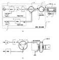
ここで、図1は本発明の実施の形態1に係る非接触ICカード読取/書込装置のブロック図である。図1(a)は本発明の実施の形態1に係る非接触ICカード読取/書込装置を示すブロック図、図1(b)は(a)の部分詳細図であり、共振回路の一例として直列共振回路を用いた場合の詳細図である。図1(a)は、非接触ICカードシステムの、読取/書込装置111と非接触ICカード112の結合に関連する部分を示したブロック図である。図1において送信データ伝送の場合は、発振器6からの搬送波を変調器7へ入力し、データDATAaによりこれを変調する。そしてこれを電力増幅器8で増幅し、マッチング回路9を経て、図1に示す方向性結合器4の端子a−b間の一次線路を介してループアンテナ5から送信する。また、電力伝送のみの場合は、発振器6からの搬送波を無変調のままで送信する。この読取/書込装置111から非接触ICカード112への送信は、電磁結合によりループアンテナ5が生成する磁束が非接触ICカード112のアンテナコイル12と鎖交し、誘起電圧を励起することにより行われる。非接触ICカード112では、アンテナコイル12の誘起電圧をICチップ13内の整流回路(図示せず)で整流して非接触ICカード内の各回路の電源として用いる。また、同じ誘起電圧を復調回路(図示せず)へ導いて読取/書込装置からのデータを復調する。
【0032】
次に、非接触ICカード112より読取/書込装置111へのデータ伝送時には、読取/書込装置は無変調の搬送波を送信して、非接触ICカードへ電力供給のみを行っている。非接触ICカード側では、ICチップ13内のメモリ(図示せず)から読み出されたデータDATAbに応じて、例えばアンテナコイル13に接続された負荷抵抗(図示せず)とスイッチ(図示せず)とからなる変調回路(図示せず)において、データの“1”、“0”ビットに応じて、このスイッチがオン、オフされる。読取/書込装置111においては、上記のようにスイッチがオン、オフすると、アンテナコイル12に対する負荷が変動する。この変動が読取/書込装置側のループアンテナ5へ電磁誘導により伝わり、ループアンテナ5側のインピーダンスが変動する。それゆえループアンテナ5側から無線受信部2側へ流れる高周波信号、すなわち無線送信部1から発した高周波信号(入射波)が方向性結合器4の端子a−b間の一次線路を経由して、ループアンテナ5側へ到達し、所望の周波数帯でのアンテナインピーダンスの変化に応じた反射波として、ループアンテナ5側より反射され、波の進行方向が逆方向の高周波信号(反射波)として、再び方向性結合器4に入力され、方向性結合器4の端子b−c間の二次線路の一端cより出力され無線受信部2へと導かれる。その結果、無線受信部2への入力信号は、上記の様に所望の周波数帯でのアンテナインピーダンスの変化に応じた高周波信号(反射波)のみとなり、理想的な回路構成となり、良好な受信特性を有する事となる。
【0033】
(実施の形態2)
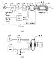
ここで、図2は本発明の実施の形態2に係る非接触ICカード読取/書込装置のブロック図である。図2(a)は本発明の実施の形態2に係る非接触ICカード読取/書込装置を示すブロック図、図2(b)は(a)の部分詳細図であり、共振回路の一例として直列共振回路を用いた場合の詳細図である。図2(a)は、非接触ICカードシステムの、読取/書込装置111と非接触ICカード112の結合に関連する部分を示したブロック図である。図2において送信データ伝送の場合は、発振器6からの搬送波を変調器7へ入力し、データDATAaによりこれを変調する。そしてこれを電力増幅器8で増幅し、マッチング回路9を経て、図2(に示すサーキュレータ14の端子a−b間の一次線路を介してループアンテナ5から送信する。また、電力伝送のみの場合は、発振器6からの搬送波を無変調のままで送信する。この読取/書込装置111から非接触ICカード112への送信は、電磁結合によりループアンテナ5が生成する磁束が非接触ICカード112のアンテナコイル12と鎖交し、誘起電圧を励起することにより行われる。非接触ICカード112では、アンテナコイル12の誘起電圧をICチップ13内の整流回路(図示せず)で整流して非接触ICカード内の各回路の電源として用いる。また、同じ誘起電圧を復調回路(図示せず)へ導いて読取/書込装置からのデータを復調する。
【0034】
次に、非接触ICカード112より読取/書込装置111へのデータ伝送時には、読取/書込装置は無変調の搬送波を送信して、非接触ICカードへ電力供給のみを行っている。非接触ICカード側では、ICチップ13内のメモリ(図示せず)から読み出されたデータDATAbに応じて、例えばアンテナコイル13に接続された負荷抵抗(図示せず)とスイッチ(図示せず)とからなる変調回路(図示せず)において、データの“1”、“0”ビットに応じて、このスイッチがオン、オフされる。読取/書込装置111においては、上記のようにスイッチがオン、オフすると、アンテナコイル12に対する負荷が変動する。この変動が読取/書込装置側のループアンテナ5へ電磁誘導により伝わり、ループアンテナ5側のインピーダンスが変動する。それゆえループアンテナ5側から無線受信部2側へ流れる高周波信号、すなわち無線送信部1から発した高周波信号(入射波)がサーキュレータ14の端子a−b間の一次線路を経由して、ループアンテナ5側へ到達し、所望の周波数帯でのアンテナインピーダンスの変化に応じた反射波として、ループアンテナ5側より反射され、波の進行方向が逆方向の高周波信号(反射波)として、再びサーキュレータ14に入力され、サーキュレータ14の端子b−c間の二次線路の一端cより出力され無線受信部2へと導かれる。その結果、無線受信部2への入力信号は、上記の様に所望の周波数帯でのアンテナインピーダンスの変化に応じた高周波信号(反射波)のみとなり、理想的な回路構成となり、良好な受信特性を有する事となる。
【0035】
(実施の形態3)
ここで図3は本発明の実施の形態3に係る非接触ICカード読取/書込装置のブロック図である。図3(a)は本発明の実施の形態3に係る非接触ICカード読取/書込装置を示すブロック図、図3(b)は(a)の部分詳細図であり、共振回路の一例として直列共振回路を用いた場合の詳細図である。図3(a)は、非接触ICカードシステムの、読取/書込装置111と非接触ICカード112の結合に関連する部分を示したブロック図である。図3において送信データ伝送の場合は、発振器6からの搬送波を変調器7へ入力し、データDATAaによりこれを変調する。そしてこれを電力増幅器8で増幅し、マッチング回路9を経て、図3に示す第一のアイソレータ15を介してループアンテナ5から送信する。また、電力伝送のみの場合は、発振器6からの搬送波を無変調のままで送信する。この読取/書込装置111から非接触ICカード112への送信は、電磁結合によりループアンテナ5が生成する磁束が非接触ICカード112のアンテナコイル12と鎖交し、誘起電圧を励起することにより行われる。非接触ICカード112では、アンテナコイル12の誘起電圧をICチップ13内の整流回路(図示せず)で整流して非接触ICカード内の各回路の電源として用いる。また、同じ誘起電圧を復調回路(図示せず)へ導いて読取/書込装置からのデータを復調する。
【0036】
次に、非接触ICカード112より読取/書込装置111へのデータ伝送時には、読取/書込装置は無変調の搬送波を送信して、非接触ICカードへ電力供給のみを行っている。非接触ICカード側では、ICチップ13内のメモリ(図示せず)から読み出されたデータDATAbに応じて、例えばアンテナコイル13に接続された負荷抵抗(図示せず)とスイッチ(図示せず)とからなる変調回路(図示せず)において、データの“1”、“0”ビットに応じて、このスイッチがオン、オフされる。読取/書込装置111においては、上記のようにスイッチがオン、オフすると、アンテナコイル12に対する負荷が変動する。この変動が読取/書込装置側のループアンテナ5へ電磁誘導により伝わり、ループアンテナ5側のインピーダンスが変動する。それゆえループアンテナ5側から無線受信部2側へ流れる高周波信号、すなわち無線送信部1から発した高周波信号(入射波)が第一のアイソレータ15の端子a−b間を経由して、ループアンテナ5側へ到達し、所望の周波数帯でのアンテナインピーダンスの変化に応じた反射波として、ループアンテナ5側より反射され、波の進行方向が逆方向の高周波信号(反射波)として、再び第二のアイソレータ16の一端cへ入力され、他端dより無線受信部2へと導かれる。その結果、無線受信部2への入力信号は、上記の様に所望の周波数帯でのアンテナインピーダンスの変化に応じた高周波信号(反射波)のみとなり、理想的な回路構成となり、良好な受信特性を有する事となる。
【0037】
以上、本発明の実施の形態1〜3について説明したが、上述したように、発振器からの搬送波は電力増幅器で増幅されるが、その増幅にはE級増幅器(Eクラスアンプ)を用いることが好ましい。E級増幅器を用いることによって、高効率動作を実現することが可能となる。よって、送信出力を上げても発熱を抑えることができる。
【0038】
【発明の効果】
以上のように本発明により、無線送信部、無線受信部間にアイソレーションをもたすことにより、無線送信部からの大振幅の高周波信号が、無線受信部内の復調回路へ流入する事を大幅に低減し、従来この大振幅の高周波信号をフィルタリングする為に必要であった復調回路前段の高性能な帯域阻止特性を有するフィルタ回路が不要となり、且つフィルタ回路の挿入損失分の電力効率低下を受けなくなる。さらに、ループアンテナとコンデンサから成る共振回路部と無線受信部間に方向性をもたすことにより、無線受信部への入力信号は、所望の周波数帯でのアンテナインピーダンスに応じた高周波信号(反射波)のみとなり、理想的な回路構成となり、良好な受信特性を有する非接触ICカード読取/書込装置を提供する事ができる。
【図面の簡単な説明】
【図1】本発明の実施の形態1に係る非接触ICカード読取/書込装置のブロック図
【図2】本発明の実施の形態2に係る非接触ICカード読取/書込装置のブロック図
【図3】本発明の実施の形態3に係る非接触ICカード読取/書込装置のブロック図
【図4】従来の非接触ICカードシステムの説明概念図
【図5】従来の非接触ICカード読取/書込装置のブロック図
【図6】従来の非接触ICカード読取/書込装置のブロック図
【符号の説明】
1 無線送信部
2 無線受信部
3 アンテナ共振回路部
4 方向性結合器
5 ループアンテナ
6 発振器
7 変調器
8 電力増幅器
9 マッチング回路
10 復調回路
12 アンテナコイル
13 ICチップ
14 サーキュレータ
15 アイソレータ
16 アイソレータ
101 非接触ICカード
102 アンテナコイル
103 ICチップ
104 ループアンテナ
105 読取/書込装置
106 発振器
107 変調器
108 電力増幅器
109 マッチング回路
110 ループアンテナ
111 読取/書込装置
112 非接触ICカード
114 復調回路
115 抵抗器
116 コンデンサ
117 抵抗器
118 コンデンサ
119 抵抗器
120 マッチングトランス
121 並列共振回路[0001]
TECHNICAL FIELD OF THE INVENTION
The present invention relates to a read / write device used in a non-contact IC card system, and more particularly to a non-contact IC card read / write in which power transmission efficiency to a non-contact IC card and data reception efficiency from the non-contact IC card are improved. It relates to an embedded device.
[0002]
[Prior art]
2. Description of the Related Art Conventionally, a read / write system using an IC card is generally called a non-contact IC card system, and is being put to practical use in, for example, a distribution system, a transportation system, an air cargo management system, and the like using a 13.56 MHz frequency band. is there.
[0003]
Here, FIG. 4 is an explanatory conceptual diagram of a conventional contactless IC card system. This system includes, as shown in FIG. 4, a
[0004]
As an example, FIG. 5 shows a read / write device of a non-contact IC card system described in (Patent Document 1). FIG. 5 is a block diagram of a conventional non-contact IC card reading / writing device, and shows a portion of the above-mentioned conventional non-contact IC card system related to the connection between the reading / writing device and the non-contact IC card. ing.
[0005]
First, in the case of transmission data transmission, a carrier wave from the
[0006]
In the case of only power transmission, the carrier from the
[0007]
Next, at the time of data transmission from the
[0008]
[Patent Document 1]
JP 2002-007976 A
[0009]
[Problems to be solved by the invention]
FIG. 5B shows a first conventional example. FIG. 5B is a detailed view of the input portion of the
[0010]
FIG. 6 is a block diagram of a conventional non-contact IC card reading / writing device. As a second conventional example, FIG. 6A shows details of the periphery of a demodulation circuit when parallel resonance is used, and a
[0011]
FIG. 6B shows, as a third conventional example, the periphery of the
[0012]
Further, FIG. 6C shows, as a fourth conventional example, a circuit configuration of a demodulation circuit input section and peripheral circuits thereof. A matching
[0013]
Further, in any of the circuits of the first to fourth conventional examples, there is no directionality in the transmission direction of power, transmission data and reception data, and in any case of the conventional example, the output from the
[0014]
Also, when receiving the received data, the change in the load impedance at the
[0015]
Further, when a high-amplitude high-frequency signal from the
[0016]
Therefore, an object of the present invention is to solve the above-mentioned conventional problems, and an object of the present invention is to provide a non-contact IC card reading / writing device having good reception characteristics.
[0017]
[Means for Solving the Problems]
The present invention provides a loop antenna that supplies power and a transmission signal to a non-contact IC card by electromagnetic induction and obtains a reception signal from the non-contact IC card by load fluctuation, and a resonance for resonating the loop antenna to a desired frequency. A circuit unit, a wireless transmission unit that supplies power and transmission data to the loop antenna via the resonance circuit unit, and a wireless reception unit that obtains a reception signal from the loop antenna via the resonance circuit unit, and a demodulation circuit from the reception signal. , Which is configured to demodulate data from a non-contact IC card, and that a resonance circuit unit, a radio transmission unit, and a radio reception unit are coupled via one of a directional coupler, a circulator, and an isolator. It is.
[0018]
BEST MODE FOR CARRYING OUT THE INVENTION
According to a first aspect of the present invention, there is provided a loop antenna that supplies power and a transmission signal to a non-contact IC card by electromagnetic induction and obtains a reception signal from the non-contact IC card by a load change. A resonance circuit unit for resonating to a frequency of, a wireless transmission unit for supplying power and transmission data to the loop antenna via the resonance circuit unit, and a wireless reception unit for acquiring a reception signal from the loop antenna via the resonance circuit unit A non-contact IC card reading / writing device configured to demodulate data from the non-contact IC card from a received signal by a demodulation circuit. It is of a configuration connected by a coupler.
[0019]
A primary line of the directional coupler is provided between the radio transmission unit and the resonance circuit unit including the loop antenna and the capacitor, and a directional coupler of the directional coupler is provided between the resonance circuit unit including the loop antenna and the capacitor and the radio reception unit. By inserting the secondary line, isolation can be provided between the wireless transmission unit and the wireless reception unit, and directionality can be provided between the resonance circuit unit including the loop antenna and the capacitor and the wireless reception unit.
[0020]
As a result, by providing isolation between the wireless transmission unit and the wireless reception unit, it is possible to greatly reduce the flow of a large-amplitude high-frequency signal from the wireless transmission unit into the demodulation circuit in the wireless reception unit. I can do it. Therefore, a filter circuit having a high-performance band rejection characteristic at the preceding stage of the demodulation circuit, which is conventionally required for filtering the large-amplitude high-frequency signal, becomes unnecessary, and the efficiency of the filter circuit due to the insertion loss is not reduced.
[0021]
Furthermore, by providing directionality between the resonance circuit unit including the loop antenna and the capacitor and the radio reception unit, a high-frequency signal flowing from the loop antenna side to the radio reception unit side, that is, a high-frequency signal (incident Wave) arrives at the loop antenna side via the primary line of the directional coupler, is reflected from the loop antenna side as a reflected wave corresponding to the antenna impedance in a desired frequency band, and the traveling direction of the wave is reverse. As a high-frequency signal (reflected wave), is again input to the directional coupler, is output from one end of the secondary line of the directional coupler, and is guided to the wireless receiver. As a result, as described above, the input signal to the radio receiving unit is only a high-frequency signal (reflected wave) corresponding to the antenna impedance in the desired frequency band, and has an ideal circuit configuration, and has a reading characteristic having good reception characteristics. / Writing device can be provided.
[0022]
According to a second aspect of the present invention, the resonance circuit unit, the wireless transmission unit, and the wireless reception unit are connected by a circulator.
[0023]
The primary line of the circulator is inserted between the radio transmission unit and the resonance circuit unit consisting of the loop antenna and the capacitor, and the secondary line of the circulator is inserted between the resonance circuit unit consisting of the loop antenna and the capacitor and the radio reception unit. Accordingly, isolation can be provided between the wireless transmission unit and the wireless reception unit, and directionality can be provided between the resonance circuit unit including the loop antenna and the capacitor and the wireless reception unit.
[0024]
As a result, by providing isolation between the wireless transmission unit and the wireless reception unit, it is possible to greatly reduce the flow of a large-amplitude high-frequency signal from the wireless transmission unit into the demodulation circuit in the wireless reception unit. I can do it. Therefore, a filter circuit having a high-performance band rejection characteristic at the preceding stage of the demodulation circuit, which is conventionally required for filtering the large-amplitude high-frequency signal, becomes unnecessary, and the efficiency of the filter circuit due to the insertion loss is not reduced.
[0025]
Further, by providing directionality between the resonance circuit unit including the loop antenna and the capacitor and the radio reception unit, a high-frequency signal flowing from the loop antenna side to the radio reception unit side, that is, a high-frequency signal generated from the radio transmission unit ( Incident wave) arrives at the loop antenna side via the primary line of the circulator, is reflected from the loop antenna side as a reflected wave corresponding to the antenna impedance in a desired frequency band, and the traveling direction of the wave is a high frequency having a reverse direction. The signal (reflected wave) is again input to the circulator, output from one end of the secondary line of the circulator, and guided to the wireless receiver. As a result, as described above, the input signal to the radio receiving unit is only a high-frequency signal (reflected wave) corresponding to the antenna impedance in the desired frequency band, and has an ideal circuit configuration, and has a reading characteristic having good reception characteristics. / Writing device can be provided.
[0026]
According to a third aspect of the present invention, the resonance circuit unit, the wireless transmission unit, and the wireless reception unit are connected by an isolator.
[0027]
By inserting the first isolator between the radio transmission unit and the resonance circuit unit including the loop antenna and the capacitor, the resonance circuit unit including the loop antenna and the capacitor, and inserting the second isolator between the radio reception unit, Isolation can be provided between the wireless transmission unit and the wireless reception unit, and directionality can be provided between the resonance circuit unit including the loop antenna and the capacitor and the wireless reception unit.
[0028]
As a result, by providing isolation between the wireless transmission unit and the wireless reception unit, it is possible to greatly reduce the flow of a large-amplitude high-frequency signal from the wireless transmission unit into the demodulation circuit in the wireless reception unit. I can do it. Therefore, a filter circuit having a high-performance band rejection characteristic before the demodulation circuit, which is conventionally required for filtering the large-amplitude high-frequency signal, becomes unnecessary, and the efficiency of the filter circuit due to the insertion loss is not reduced.
[0029]
Further, by providing directionality between the resonance circuit unit including the loop antenna and the capacitor and the radio reception unit, a high-frequency signal flowing from the loop antenna side to the radio reception unit side, that is, a high-frequency signal generated from the radio transmission unit ( Incident wave) arrives at the loop antenna side via the first isolator, is reflected from the loop antenna side as a reflected wave corresponding to the antenna impedance in a desired frequency band, and the wave travels in the opposite direction. The signal (reflected wave) is again input to the second isolator, output from one end of the second isolator, and guided to the wireless receiver. As a result, as described above, the input signal to the radio receiving unit is only a high-frequency signal (reflected wave) corresponding to the antenna impedance in the desired frequency band, and has an ideal circuit configuration, and has a reading characteristic having good reception characteristics. / Writing device can be provided.
[0030]
Hereinafter, an embodiment of the present invention will be described with reference to FIGS. Note that the definition of a non-contact IC card in the present invention is not limited to a so-called card, but is a wireless communication medium capable of performing communication with a reading / writing device in a non-contact manner. Therefore, it includes what is called an IC tag, an ID tag, and an identification label depending on the use.
[0031]
(Embodiment 1)
Here, FIG. 1 is a block diagram of a non-contact IC card reading / writing device according to
[0032]
Next, at the time of data transmission from the
[0033]
(Embodiment 2)
Here, FIG. 2 is a block diagram of a non-contact IC card reading / writing device according to
[0034]
Next, at the time of data transmission from the
[0035]
(Embodiment 3)
Here, FIG. 3 is a block diagram of a non-contact IC card reading / writing device according to
[0036]
Next, at the time of data transmission from the
[0037]
As described above, the first to third embodiments of the present invention have been described. As described above, the carrier wave from the oscillator is amplified by the power amplifier, and a class E amplifier (E class amplifier) is used for the amplification. preferable. By using a class E amplifier, high-efficiency operation can be realized. Therefore, heat generation can be suppressed even when the transmission output is increased.
[0038]
【The invention's effect】
As described above, according to the present invention, by providing isolation between the wireless transmission unit and the wireless reception unit, a large-amplitude high-frequency signal from the wireless transmission unit can be largely prevented from flowing into the demodulation circuit in the wireless reception unit. This eliminates the need for a filter circuit having a high-performance band rejection characteristic at the previous stage of the demodulation circuit, which is conventionally required for filtering the large-amplitude high-frequency signal, and reduces the power efficiency by the insertion loss of the filter circuit. I will not receive it. Further, by providing directivity between the resonance circuit unit including the loop antenna and the capacitor and the radio reception unit, an input signal to the radio reception unit can receive a high-frequency signal (reflected signal) corresponding to the antenna impedance in a desired frequency band. Wave), an ideal circuit configuration is obtained, and a non-contact IC card reading / writing device having good reception characteristics can be provided.
[Brief description of the drawings]
FIG. 1 is a block diagram of a non-contact IC card reading / writing device according to a first embodiment of the present invention;
FIG. 2 is a block diagram of a non-contact IC card reading / writing device according to a second embodiment of the present invention;
FIG. 3 is a block diagram of a non-contact IC card reading / writing device according to a third embodiment of the present invention;
FIG. 4 is an explanatory conceptual diagram of a conventional contactless IC card system.
FIG. 5 is a block diagram of a conventional non-contact IC card reading / writing device.
FIG. 6 is a block diagram of a conventional non-contact IC card reading / writing device.
[Explanation of symbols]
1 wireless transmitter
2 Radio receiver
3 Antenna resonance circuit
4 directional coupler
5 loop antenna
6 oscillator
7 Modulator
8 Power amplifier
9 Matching circuit
10 Demodulation circuit
12 Antenna coil
13 IC chip
14 Circulator
15 Isolator
16 Isolator
101 Non-contact IC card
102 Antenna coil
103 IC chip
104 loop antenna
105 read / write device
106 oscillator
107 modulator
108 power amplifier
109 Matching circuit
110 loop antenna
111 read / write device
112 Non-contact IC card
114 Demodulation circuit
115 resistor
116 Capacitor
117 resistor
118 capacitor
119 resistor
120 Matching transformer
121 Parallel resonance circuit
Claims (3)
Translated fromJapanesePriority Applications (4)
| Application Number | Priority Date | Filing Date | Title |
|---|---|---|---|
| JP2002372222AJP2004206245A (en) | 2002-12-24 | 2002-12-24 | Non-contact IC card reading / writing device |
| EP03029458AEP1434160A3 (en) | 2002-12-24 | 2003-12-19 | Non-contact IC card reading/writing apparatus |
| EP05022151.4AEP1615158B1 (en) | 2002-12-24 | 2003-12-19 | Contactless smart card reader |
| US10/743,899US7164344B2 (en) | 2002-12-24 | 2003-12-24 | Non-contact IC card reading/writing apparatus |
Applications Claiming Priority (1)
| Application Number | Priority Date | Filing Date | Title |
|---|---|---|---|
| JP2002372222AJP2004206245A (en) | 2002-12-24 | 2002-12-24 | Non-contact IC card reading / writing device |
Publications (1)
| Publication Number | Publication Date |
|---|---|
| JP2004206245Atrue JP2004206245A (en) | 2004-07-22 |
Family
ID=32810881
Family Applications (1)
| Application Number | Title | Priority Date | Filing Date |
|---|---|---|---|
| JP2002372222APendingJP2004206245A (en) | 2002-12-24 | 2002-12-24 | Non-contact IC card reading / writing device |
Country Status (1)
| Country | Link |
|---|---|
| JP (1) | JP2004206245A (en) |
Cited By (6)
| Publication number | Priority date | Publication date | Assignee | Title |
|---|---|---|---|---|
| JP2008182458A (en)* | 2007-01-24 | 2008-08-07 | National Univ Corp Shizuoka Univ | Inductive link |
| JP2012503469A (en)* | 2008-09-17 | 2012-02-02 | クゥアルコム・インコーポレイテッド | Transmitter for wireless power transmission |
| US8432070B2 (en) | 2008-08-25 | 2013-04-30 | Qualcomm Incorporated | Passive receivers for wireless power transmission |
| US8872385B2 (en) | 2010-12-22 | 2014-10-28 | Panasonic Corporation | Wireless power transmission system |
| US8947041B2 (en) | 2008-09-02 | 2015-02-03 | Qualcomm Incorporated | Bidirectional wireless power transmission |
| US9054745B2 (en) | 2010-12-22 | 2015-06-09 | Electronics And Telecommunications Research Institute | Apparatus for transmitting/receiving energy using a resonance structure in an energy system |
- 2002
- 2002-12-24JPJP2002372222Apatent/JP2004206245A/enactivePending
Cited By (8)
| Publication number | Priority date | Publication date | Assignee | Title |
|---|---|---|---|---|
| JP2008182458A (en)* | 2007-01-24 | 2008-08-07 | National Univ Corp Shizuoka Univ | Inductive link |
| US8432070B2 (en) | 2008-08-25 | 2013-04-30 | Qualcomm Incorporated | Passive receivers for wireless power transmission |
| US8947041B2 (en) | 2008-09-02 | 2015-02-03 | Qualcomm Incorporated | Bidirectional wireless power transmission |
| JP2012503469A (en)* | 2008-09-17 | 2012-02-02 | クゥアルコム・インコーポレイテッド | Transmitter for wireless power transmission |
| US8532724B2 (en) | 2008-09-17 | 2013-09-10 | Qualcomm Incorporated | Transmitters for wireless power transmission |
| US9425653B2 (en) | 2008-09-17 | 2016-08-23 | Qualcomm Incorporated | Transmitters for wireless power transmission |
| US8872385B2 (en) | 2010-12-22 | 2014-10-28 | Panasonic Corporation | Wireless power transmission system |
| US9054745B2 (en) | 2010-12-22 | 2015-06-09 | Electronics And Telecommunications Research Institute | Apparatus for transmitting/receiving energy using a resonance structure in an energy system |
Similar Documents
| Publication | Publication Date | Title |
|---|---|---|
| US7164344B2 (en) | Non-contact IC card reading/writing apparatus | |
| JP4380239B2 (en) | Non-contact IC card reader / writer | |
| CA2215257C (en) | Power transmission system, ic card and information communication system using ic card | |
| CN102017438B (en) | Radio frequency communication device and method for operating same | |
| EP0575013A1 (en) | System for the contactless exchange of data, and responder for use in such a system | |
| JPH06204922A (en) | Two-way communication system | |
| JP2001076111A (en) | Resonance circuit | |
| JP3649374B2 (en) | Antenna device and card-like storage medium | |
| CN100405737C (en) | Electronic circuit, modulation method, information processing apparatus, and information processing method | |
| WO2001067413A1 (en) | Electrostatic and electromagnetic communication systems and combinations thereof | |
| EP1486903A2 (en) | Reader/writer for performing efficient transmission/reception with no-battery information storage medium | |
| JP4657574B2 (en) | Non-contact IC card reader / writer | |
| JP2008028791A (en) | Class E amplifier, reader / writer and document management system using the same | |
| JP2008301241A (en) | Loop antenna and wireless transceiver including loop antenna | |
| JP2004206245A (en) | Non-contact IC card reading / writing device | |
| JP2006180491A (en) | Electromagnetic transponder with no autonomous power supply | |
| US20100013605A1 (en) | Data carrier and data carrier system | |
| JP3449621B2 (en) | Reader / writer device for non-contact IC card system | |
| JP3003482B2 (en) | Radio frequency code identification method | |
| JP4666738B2 (en) | Non-contact IC card reader / writer device | |
| JP4015268B2 (en) | Reader / writer | |
| JP3194715B2 (en) | Reader / writer device for non-contact IC card system | |
| JP4843994B2 (en) | Reader and data carrier system | |
| JP2007058381A (en) | Antenna circuit | |
| WO2004097725A1 (en) | Communication device and wireless tag reader/writer |
Legal Events
| Date | Code | Title | Description |
|---|---|---|---|
| A621 | Written request for application examination | Free format text:JAPANESE INTERMEDIATE CODE: A621 Effective date:20051209 | |
| RD01 | Notification of change of attorney | Free format text:JAPANESE INTERMEDIATE CODE: A7421 Effective date:20060112 | |
| A977 | Report on retrieval | Free format text:JAPANESE INTERMEDIATE CODE: A971007 Effective date:20080421 | |
| A131 | Notification of reasons for refusal | Free format text:JAPANESE INTERMEDIATE CODE: A131 Effective date:20080507 | |
| A521 | Request for written amendment filed | Free format text:JAPANESE INTERMEDIATE CODE: A523 Effective date:20080627 | |
| A02 | Decision of refusal | Free format text:JAPANESE INTERMEDIATE CODE: A02 Effective date:20081014 |