JP2004201467A - Inverter mounted in polyphase alternating-current rotating electric machine - Google Patents
Inverter mounted in polyphase alternating-current rotating electric machineDownload PDFInfo
- Publication number
- JP2004201467A JP2004201467AJP2002370038AJP2002370038AJP2004201467AJP 2004201467 AJP2004201467 AJP 2004201467AJP 2002370038 AJP2002370038 AJP 2002370038AJP 2002370038 AJP2002370038 AJP 2002370038AJP 2004201467 AJP2004201467 AJP 2004201467A
- Authority
- JP
- Japan
- Prior art keywords
- phase
- arm element
- electric machine
- cooling fin
- rotating electric
- Prior art date
- Legal status (The legal status is an assumption and is not a legal conclusion. Google has not performed a legal analysis and makes no representation as to the accuracy of the status listed.)
- Granted
Links
- 238000001816coolingMethods0.000claimsabstractdescription143
- 239000004065semiconductorSubstances0.000claimsabstractdescription59
- 238000004891communicationMethods0.000claimsdescription16
- 230000000149penetrating effectEffects0.000claimsdescription6
- 238000004804windingMethods0.000claimsdescription6
- 238000005520cutting processMethods0.000claimsdescription2
- 230000017525heat dissipationEffects0.000claimsdescription2
- 238000004080punchingMethods0.000claimsdescription2
- 238000010276constructionMethods0.000abstract1
- 239000000758substrateSubstances0.000description10
- 239000004020conductorSubstances0.000description8
- 230000001360synchronised effectEffects0.000description5
- RYGMFSIKBFXOCR-UHFFFAOYSA-NCopperChemical compound[Cu]RYGMFSIKBFXOCR-UHFFFAOYSA-N0.000description4
- 230000015556catabolic processEffects0.000description4
- 229910052802copperInorganic materials0.000description4
- 239000010949copperSubstances0.000description4
- 238000001514detection methodMethods0.000description4
- 230000002093peripheral effectEffects0.000description3
- 239000003990capacitorSubstances0.000description2
- 238000009499grossingMethods0.000description2
- 230000004048modificationEffects0.000description2
- 238000012986modificationMethods0.000description2
- 125000006850spacer groupChemical group0.000description2
- 230000004323axial lengthEffects0.000description1
- 238000010586diagramMethods0.000description1
- 239000003822epoxy resinSubstances0.000description1
- 238000000605extractionMethods0.000description1
- 238000005304joiningMethods0.000description1
- 238000004519manufacturing processMethods0.000description1
- 238000000034methodMethods0.000description1
- 238000000465mouldingMethods0.000description1
- 229920000647polyepoxidePolymers0.000description1
- 230000005855radiationEffects0.000description1
- 229920005989resinPolymers0.000description1
- 239000011347resinSubstances0.000description1
- 238000007789sealingMethods0.000description1
- 238000007493shaping processMethods0.000description1
- XLYOFNOQVPJJNP-UHFFFAOYSA-NwaterSubstancesOXLYOFNOQVPJJNP-UHFFFAOYSA-N0.000description1
Images


Landscapes
- Inverter Devices (AREA)
Abstract
Description
Translated fromJapanese【0001】
【発明の属する技術分野】
本発明は、多相交流回転電機搭載インバータに関する。
【0002】
【従来の技術】
従来、直流電源と多相交流回転電機の電機子巻線との間に電力授受可能に介設されて、この電機子巻線に多相交流電圧を印加するインバータを交流回転電機に一体化することにより、小型軽量化や配線損失の低減を図った多相交流回転電機搭載インバータが提案されている。
【0003】
このインバータは、通常では、それぞれトランジスタからなる相数分又はその整数倍の上アーム素子(ハイサイド素子)と、それぞれトランジスタからなる相数分又はその整数倍の下アーム素子(ローサイド素子)を有し、同一相の上アーム素子と下アーム素子の交流側主電極は直列接続されて電機子巻線の各端子に接続され、上アーム素子の直流側主電極は正側ライン(高位直流ラインをいう)を通じて直流電源の正側電極端子(以下、正側端子ともいう)に接続され、下アーム素子の直流側主電極は負側ライン(低位直流ラインをいう)を通じて直流電源の低位電極端子(以下、負側端子ともいう)に接続されている。インバータの各トランジスタは、コントローラからの制御信号によりスイッチングされて多相交流電圧を発生させ、多相交流回転電機を駆動したり(以下、電動駆動ともいう)、あるいは多相交流回転電機が発生する多相交流電圧を同期整流したり(以下、同期整流駆動ともいう)する。
【0004】
上アーム素子及び下アーム素子は、MOSトランジスタ、バイポーラトランジスタ、IGBTなどにより構成されるが、逆並列接続ダイオードを持たないバイポーラトランジスタ、IGBTを採用する場合には、接合ダイオードをそれらと逆並列接続するのが通常である。
【0005】
これら上アーム素子及び下アーム素子を構成するこれらのトランジスタとしては、多数キャリヤ電荷が電子であるタイプのものが、抵抗損失低減及び素子コスト低減の点で採用される。すなわち、MOSトランジスタにおいてはnチャンネルMOSトランジスタを、バイポーラトランジスタにおいてはnpnトランジスタを、IGBTにおいては絶縁ゲート付きのnpnトランジスタを採用する以外の選択は現状ではありえない。
【0006】
上記した多相交流回転電機搭載インバータに関連する技術として、従来の車両用交流発電機に搭載される三相全波整流回路(レクチファイア)がある。このレクチファイアは、三相交流回転電機の後端面に位置して互いに軸方向に所定間隔を隔てて配置され、それぞれ径方向かつ周方向に延在する略円弧状の正側プレート及び負側プレートを有し、各相の上アーム側のダイオードは、正側ラインをなす放熱部材兼用共通電極板である正側プレートに共通固定され、各相の下アーム側のダイオードは、負側ラインをなす放熱部材兼用共通電極板である負側プレートに共通固定されている。
【0007】
【発明が解決しようとする課題】
上記した多相交流回転電機搭載インバータにおいて、上記車両用交流発電機のレクチファイアと同様に、冷却機能及び集電機能(配線機能)を兼ねる円弧状の放熱部材兼用共通電極板(以下、冷却フィンともいう)により正側プレートと負側プレート(直流電源の低位電極端子に接続されるならば実際に接地されていなくてもよい)を構成し、これら二枚の冷却フィンをを軸方向にずらせて多相交流回転電機のハウジング端面近傍に配置すれば、多相交流回転電機搭載インバータの冷却機能及び集電機能を従来の車両用交流発電機と同様に良好に確保しつつ、その装置体格を従来の車両用交流発電機と同程度にコンパクト化できることが期待される。
【0008】
しかしながら、多相交流回転電機のインバータの上アーム素子を正側プレートに共通搭載し、その下アーム素子を負側プレートに共通搭載することは、現状では以下の理由により困難である。
【0009】
つまり、下アーム素子を構成するトランジスタは内部に耐圧層(いわゆるコレクタ耐圧層又はドレイン耐圧層)を有する半導体チップにより構成され、この耐圧層は半導体チップの基板の直上に形成される。したがって、トランジスタの多数キャリヤを電子とする場合、言い換えれば、nチャンネルMOSトランジスタ、npnトランジスタ、n型のエミッタ、コレクタを有するIGBT(n型のIGBT)を採用する場合、半導体チップの基板側の電極は下アーム素子の交流側主電極を構成するので、半導体チップの表面側の主電極が直流側主電極として負側プレートに接続されることになる。トランジスタの制御電極(ゲート電極又はベース電極)は半導体製造プロセス上、半導体チップの表面に形成する他はないので、結局、各相の下アーム素子を構成するトランジスタの直流側主電極を負側プレートに密着接合すると、この直流側主電極に隣接して半導体チップの表面に形成される制御電極も負側プレートに密着接合されてしまい、外部に取り出すことが困難になってしまうため、各相の下アーム素子をなすトランジスタを良好な放熱を確保しつつ負側プレートに共通固定することが困難となる。つまり、多相交流回転電機搭載インバータでは、車両用交流発電機のレクチファイアのように2枚の冷却フィンの一方に各相の上アーム素子を、他方に各相の下アーム素子を固定するという冷却集電構造を採用することができない。
【0010】
本発明は上記問題点に鑑みなされたものであり、優れた冷却集電構造を確保しつつ簡素な構造を有してコンパクト化が可能な多相交流回転電機搭載インバータを提供することをその目的としている。
【0011】
【課題を解決するための手段】
本発明の多相交流回転電機搭載インバータは、相数の整数倍の上アーム素子と、相数の整数倍の下アーム素子とを有し、同一相の前記上アーム素子と前記下アーム素子の交流側主電極は、直列接続されて多相交流回転電機の電機子巻線の相端子に接続され、前記上アーム素子の直流側主電極は、正側ラインを通じて直流電源の正側端子に接続され、前記下アーム素子の直流側主電極は、負側ラインを通じて前記直流電源の負側端子に接続され、前記上アーム素子及び下アーム素子はそれぞれ、電子を主要なキャリア電荷とするトランジスタをなす半導体チップ又は半導体モジュールを含む多相交流回転電機搭載インバータにおいて、
前記正側ラインは、前記多相交流回転電機のハウジングの端壁近傍に位置して略径方向及び略周方向に延在して放熱部材兼用共通電極板を構成する平板状の+冷却フィンからなり、前記負側ラインは、前記+冷却フィンから軸方向に所定間隔離れるとともに略径方向及び略周方向に延在して放熱部材兼用共通電極板を構成する平板状の−冷却フィンからなり、前記各相の上アーム素子の直流側主電極は、上アーム素子用の前記半導体チップ又は半導体モジュールの半導体基板側の主面に設けられて、前記+冷却フィンの表面に互いに周方向へ所定間隔を隔てて共通固定され、前記各相の下アーム素子の直流側主電極は、下アーム素子用の前記半導体チップ又は半導体モジュールの表面側の主面に設けられて、前記−冷却フィンの表面に互いに周方向へ所定間隔を隔てて共通固定され、前記−冷却フィンは、前記半導体チップ又は前記半導体モジュールの前記表面側の主面に前記直流側主電極に隣接して設けられた前記各相の下アーム素子の制御電極を露出させる複数の制御電極配線背面側取り出し用窓を有することを特徴としている。
【0012】
なお、ここでいう半導体モジュールとは、半導体チップの両側に少なくとも主電極をなす導体板を有し、側面を樹脂封止された構造を意味する。半導体モジュールでは、通常、半導体モジュールの表面側の導体板に隣接して制御電極をなす導体板が配置され、この制御電極用の導体板と主電極用の導体板との間も樹脂封止される。
【0013】
すなわち、この発明によれば、各相の下アーム素子の直流側主電極(nチャンネルMOSトランジスタでは半導体チップの表面側の主電極)が、−冷却フィンの表面にそれぞれ固定される。このため、ハウジングの端壁面に沿って延在する−冷却フィンは、負側ラインを構成すると共に各相の下アーム素子を良好に冷却することができる。
【0014】
更に、この発明の−冷却フィンは、各下アーム素子をなす半導体チップ又は半導体モジュールの表面側電極すなわち直流側主電極に隣接して半導体チップの表面側主面の制御電極を露出させる制御電極配線背面側取り出し用窓を下アーム素子数分有している。
【0015】
これにより、各下アーム素子の表面側の主電極を−冷却フィンの表面に密着させた場合でも、各下アーム素子の制御電極は、これらの窓から個別に露出することができるため、これらの窓を貫通する制御信号線の先端をなんら支障無く、各下アーム素子の制御電極に接続することができるうえ、接続作業も簡単となる。その結果、優れた冷却集電構造を確保しつつ、冷却用の+冷却フィンと−冷却フィンがインバータの正側ラインと負側ラインとを兼ねることができるので、簡素な配線構造と小さい抵抗損失を有してコンパクト化が可能な多相交流回転電機搭載インバータを実現することができる。
【0016】
好適な態様において、前記制御電極配線背面側取り出し用窓は、前記−冷却フィンの辺の途中を切り欠いて形成された溝部からなることを特徴とする。すなわち、この態様では、半導体チップ又は半導体モジュールを−冷却フィンの周辺部に配置することにより、窓を溝部により構成することができる。溝部は一辺が開口しているので、制御信号線の接続作業が容易となる。
【0017】
好適な態様において、前記制御電極配線背面側取り出し用窓は、前記−冷却フィンを打ち抜いて形成された孔部からなることを特徴とする。このようにすれば、半導体チップ又は半導体モジュールを−冷却フィンの幅方向中央部に配置することができるので、その冷却性を向上することができる。
【0018】
好適な態様において、前記−冷却フィン及び+冷却フィンは、円弧状に形成されて、界磁コイル型の前記多相交流回転電機のブラシと軸方向に重なり、周方向に重ならない位置に配置されていることを特徴とする。このようにすれば、界磁コイル型の多相交流回転電機の軸長を短縮することができる。
【0019】
好適な態様において、前記下アーム素子の前記制御電極は、前記窓を貫通して軸方向に延在する制御信号線の先端に接続されている。これにより、制御信号線を−冷却フィンの裏側に沿いつつ延設することができ、配線を簡素化することができる。また、各相の下アーム素子を−冷却フィンに共通固定できると共に、簡単にコントローラと下アーム素子の制御電極とを簡単、確実に接続することが可能となる。
【0020】
なお、この窓を貫通した制御信号線の先端を下アーム素子の制御電極に接合してもよく、あるいは、下アーム素子の制御電極に基端部が接合されてこの窓を貫通して−冷却フィンの裏側に突出する制御端子を予め下アーム素子に取り付けておき、制御信号線をこの制御端子の先端部に接続しても良い。この場合には、制御信号線(又は通信線)を窓に突っ込んだ後、その先端を半導体チップの表面側主面に形成された制御電極(通信電極)に接合する作業を省略でき、配線作業を簡素化することができる。
【0021】
好適な態様において、前記下アーム素子は、前記制御信号線貫通用の窓に露出して通信線が接続される通信用電極を有することを特徴とする。これにより、構造を複雑化することなく、各相の下アーム素子の温度や電流などを簡単、確実に検出することができる。
【0022】
【発明の実施の形態】
本発明の多相交流回転電機搭載インバータの好適な態様を図面を参照して以下に説明する。
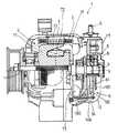
(車両用交流発電機1)
図1において、車両用発電電動機1は、三相界磁コイル型同期機であって、ロータ2、ステータ3、ハウジング4、電源端子6、回転軸7、ブラシ8、スリップリング9、コネクタと一体のレギュレータ11を有し、インバータ5を搭載している。レギュレータ11は界磁電流を断続制御するが周知のため説明は省略する。
【0023】
ステータ3は、ステータコイル31と、ハウジング4の周壁内周面に固定されたステータコア32とを有し、ステータコイル31はステータコア32の各スロットに巻装されている。この種の同期機自体は周知である。なお、本発明は、その他の種類の同期機に採用されることができることはもちろんである。
【0024】
ロータ3は、ハウジング4に回転自在に支持された回転軸7に固定されたロータコア71と、ロータコア71に巻装された界磁コイル72とを有し、ステータ3の径内側に配置されている。ステータコイル31は三相電機子巻線であって、その三つの交流端子は、インバータ5の各交流端子に接続されている。界磁コイル72は、ブラシ8およびスリップリング9を通じて給電された界磁電流により磁化されて界磁磁界を発生する。界磁電流は、図示しないレギュレータにより調整される。
(インバータ5)
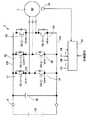
インバータ5は、図2に示すように、バッテリ10から給電されて、車両用発電電動機1のステータコイル31の各交流端子に三相交流電圧を印加する。
【0025】
51はU相上アーム素子、52はV相上アーム素子、53はW相上アーム素子、54はU相下アーム素子、55はV相下アーム素子、56はW相下アーム素子であり、それぞれMOSトランジスタにより構成されているが、ダイオード付きのバイポーラトランジスタ又はIGBTによっても構成できることはもちろんである。各トランジスタ51〜56は、直流側主電極と交流側主電極と制御電極(ゲート電極)とを有している。上アーム素子51〜53は、交流側主電極の電位V1〜V3を出力する端子(通信用電極)を有し、下アーム素子54〜56は、直流側主電極の電位V4〜V6を出力する端子(通信用電極)を有している。その他、ミラー電流検出、温度検出のための端子を追加してもよい。
【0026】
57は、ゲートコントローラであり、回転角センサ58からの信号や上記通信端子からの信号に基づいて各トランジスタのゲート電圧G1〜G6を作成して各トランジスタ51〜56のゲート電極すなわち制御電極に送る。なお、各相の交流電流を検出する電流センサを追加してもよい。59は平滑コンデンサである。この種のインバータ5自体はよく知られているため、これ以上の説明は省略する。
(インバータ5の構造)
インバータ5、特にそのトランジスタ51〜56の構造について以下に説明する。
【0027】
図1において、100は−冷却フィン、101は+冷却フィン、102はU相冷却フィン、106はステータコイル31から突出するその相端子(実際には3本であるが1本のみ図示)である。+冷却フィン101の一端には、電源端子6が固定され、−冷却フィン100の一端はモータハウジング4を通じて接地されている。
【0028】
−冷却フィン100は、モータハウジング4の後端壁に近接して径方向及び周方向に延設される円弧状の銅輪板からなり、+冷却フィン101は、−冷却フィン100から軸方向に所定間隔離れて径方向及び周方向に延設される円弧状の銅輪板からなり、U相冷却フィン102は、−冷却フィン100と+冷却フィン101との間に配置されて径方向及び周方向に延設される円弧状の銅輪板からなる。U相冷却フィン102の周方向長は、−冷却フィン100、+冷却フィン101の周方向長の1/3以下とされている。その他、U相冷却フィン102と略同一形状をもつV相冷却フィン、W相冷却フィンが、U相冷却フィン102と軸方向同位置にて、互いに周方向異なる位置に順番に配置されている。U相冷却フィン102は、図1に示すように、U相端子106に接合され、同様に、V相冷却フィン、W相冷却フィンも、ステータコイル31から軸方向に突出する図示しないV相端子、W相端子に接合されている。
【0029】
−冷却フィン100及び+冷却フィン101は、ブラシ8と軸方向に重なる位置に設けられているが、円弧状に形成された冷却フィン100、101及び各相の冷却フィンは、ブラシ8及びその径方向外側に配置されたレギュレータ11と干渉しない周方向位置に配置されている。
【0030】
図1に示すように、MOSトランジスタチップからなるU相の上アーム素子51は、+冷却フィン101とU相冷却フィン102との間に配置されている。上アーム素子51の直流側主電極はMOSトランジスタチップ(半導体チップ)の基板側の主面に形成されて+冷却フィン101に接合されている。上アーム素子51の交流側主電極はMOSトランジスタチップ(半導体チップ)の表面側の主面に形成されてU相冷却フィン102に接合されている。後述するように、U相冷却フィン102には上アーム素子51を構成するMOSトランジスタチップの表面側の主面に形成されるその制御電極(ゲート電極G1)に制御信号線を接続するために、孔(図1では図示省略)が設けられている。
【0031】
同様に、MOSトランジスタチップからなるV相の上アーム素子52も、+冷却フィン101とV相冷却フィン(図1では図示せず)との間に配置されている。上アーム素子52の直流側主電極はMOSトランジスタチップ(半導体チップ)の基板側の主面に形成されて+冷却フィン101に接合されている。上アーム素子52の交流側主電極はMOSトランジスタチップ(半導体チップ)の表面側の主面に形成されてV相冷却フィン(図1では図示せず)に接合されている。後述するように、V相冷却フィン(図1では図示せず)には上アーム素子52を構成するMOSトランジスタチップの表面側の主面に形成されるその制御電極(ゲート電極G2)に制御信号線を接続するために、孔(図1では図示省略)が設けられている。
【0032】
同様に、MOSトランジスタチップからなるW相の上アーム素子53も、+冷却フィン101とW相冷却フィン(図1では図示せず)との間に配置されている。上アーム素子53の直流側主電極はMOSトランジスタチップ(半導体チップ)の基板側の主面に形成されて+冷却フィン101に接合されている。上アーム素子53の交流側主電極はMOSトランジスタチップ(半導体チップ)の表面側の主面に形成されてW相冷却フィン(図1では図示せず)に接合されている。後述するように、W相冷却フィン(図1では図示せず)には上アーム素子53を構成するMOSトランジスタチップの表面側の主面に形成されるその制御電極(ゲート電極G3)に制御信号線を接続するために、孔(図1では図示省略)が設けられている。
【0033】
図1に示すように、MOSトランジスタチップからなるU相の下アーム素子54は、−冷却フィン100とU相冷却フィン102との間に配置されている。下アーム素子54の直流側主電極はMOSトランジスタチップ(半導体チップ)の表面側の主面に形成されて−冷却フィン100に接合されている。下アーム素子54の交流側主電極はMOSトランジスタチップ(半導体チップ)の基板側の主面に形成されてU相冷却フィン102に接合されている。後述するように、−冷却フィン100には下アーム素子54を構成するMOSトランジスタチップの表面側の主面に形成されるその制御電極(ゲート電極G4)に制御信号線を接続するために、孔(図1では図示省略)が設けられている。
【0034】
同様に、MOSトランジスタチップからなるV相の下アーム素子55は、−冷却フィン100とV相冷却フィン(図1では図示せず)との間に配置されている。下アーム素子55の直流側主電極はMOSトランジスタチップ(半導体チップ)の表面側の主面に形成されて−冷却フィン100に接合されている。下アーム素子55の交流側主電極はMOSトランジスタチップ(半導体チップ)の基板側の主面に形成されてV相冷却フィン(図1では図示せず)に接合されている。後述するように、−冷却フィン100には下アーム素子55を構成するMOSトランジスタチップの表面側の主面に形成されるその制御電極(ゲート電極G5)に制御信号線を接続するために、孔(図1では図示省略)が設けられている。
【0035】
同様に、MOSトランジスタチップからなるW相の下アーム素子56は、−冷却フィン100とW相冷却フィン(図1では図示せず)との間に配置されている。下アーム素子56の直流側主電極はMOSトランジスタチップ(半導体チップ)の表面側の主面に形成されて−冷却フィン100に接合されている。下アーム素子56の交流側主電極はMOSトランジスタチップ(半導体チップ)の基板側の主面に形成されてW相冷却フィン(図1では図示せず)に接合されている。後述するように、−冷却フィン100には下アーム素子56を構成するMOSトランジスタチップの表面側の主面に形成されるその制御電極(ゲート電極G6)に制御信号線を接続するために、孔(図1では図示省略)が設けられている。
【0036】
上記各MOSトランジスタチップ51〜56はNチャンネルMOSトランジスタが形成された半導体チップである。
【0037】
−冷却フィン100は直接又はスペーサ(図1では図示せず)を介してモータハウジング4の後端壁に固定されている。各交流端子としてのU相冷却フィン102、V相冷却フィン、W相冷却フィン、+冷却フィン101は、電気絶縁性のスペーサ(図1では図示せず)を介して−冷却フィン100に固定されている。各MOSトランジスタチップ51〜56は、上記接合の後、エポキシ樹脂などにより封止されている。
【0038】
結局、この実施例では、インバータ5の正側ラインを+冷却フィン101により構成している。すなわち、+冷却フィン101は、放熱部材兼用共通電極板となっている。また、インバータ5の負側ラインを−冷却フィン100により構成している。すなわち、−冷却フィン100は、放熱部材兼用共通電極板となっている。更に、インバータ5のU相配線の一部をU相冷却フィン102により構成し、同様に、V相配線、W相配線の各一部をV相冷却フィン、W相冷却フィンにより構成している。すなわち、各相の冷却フィンは放熱部材兼用共通電極板となっている。更に、これらの冷却フィンを、軸方向に互いに離れて3カ所に分置して、それぞれ径方向及び周方向に延設している。このような冷却フィン群の配置により、カバー12に設けた外気吸入孔(図示省略)からカバー12内に軸方向又は径内方向へ導入された外気は良好に各冷却フィンを冷却することができ、各冷却フィンを通じて各MOSトランジスタチップを冷却することができる。各冷却フィンを冷却した外気はモータハウジング4の後壁面に設けた外気流入孔からモータハウジング4内に導入される。この外気の流れはロータ2に設けたファン13により形成され、モータハウジング4の周壁に設けた排気孔から外部に排出される。
【0039】
このような開放冷却モータ構造の代わりにモータ及びインバータ5を密閉型とすることも可能である。この場合には、インバータ5の各冷却フィンは、水冷されるモータハウジング4に密着することができる。もちろん、この場合、−冷却フィン100を除く他の冷却フィンは絶縁フィルムを介してモータハウジング4に密着される。その他、水冷パイプやヒートパイプなどをこれら冷却フィンに直接密着することもできる。
【0040】
また、磁石式の同期機においては、レギュレータ11やブラシ8を省略することができるので、インバータ5の−冷却フィン100や+冷却フィン101は輪板状に形成することができる。
【0041】
(MOSトランジスタチップの配置)
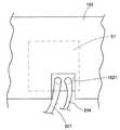
上アーム素子51の配置を図3に示す。201は、上アーム素子51をなすMOSトランジスタチップの表面側の主面に形成される交流側主電極の領域であり、U相冷却フィン102に半田付けされている。202は、上アーム素子51をなすMOSトランジスタチップの基板側の主面に形成される直流側主電極の領域であり、+冷却フィン101に半田付けされている。203は、上アーム素子51をなすMOSトランジスタチップの表面側の主面に形成される制御電極の領域であり、ボンディングワイヤ204に接続されている。ボンディングワイヤ204は、U相冷却フィン102の溝部1021を貫通してU相冷却フィン102の裏側に取り出され、図示しないフレキシブルテープなどの配線によりコントローラ57に達している。この溝部1021には通信線をなすボンディングワイヤ(図3では図示せず)も貫通しており、この通信線をなすボンディングワイヤは、MOSトランジスタチップ51の制御電極の領域に隣接する電位V1検出領域に接合されている。ボンディングワイヤ以外にたとえば図4に示す窓貫通端子を用いてもよい。
【0042】
下アーム素子54の配置を図4に示す。201は、下アーム素子54をなすMOSトランジスタチップの表面側の主面に形成される直流側主電極の領域であり、−冷却フィン100に半田付けされている。202は、下アーム素子54をなすMOSトランジスタチップの基板側の主面に形成される交流側主電極の領域であり、U相冷却フィン102にに半田付けされている。203は、上アーム素子51をなすMOSトランジスタチップの表面側の主面に形成される制御電極の領域であり、窓貫通端子205に半田付けされている。窓貫通端子205は、−冷却フィン100の孔部1022を貫通して−冷却フィン100の裏側に取り出され、図示しないバスバーなどの配線によりコントローラ57に達している。この孔部1022には通信線をなす窓貫通端子(図4では図示せず)も貫通しており、この通信線をなす窓貫通端子は、MOSトランジスタチップ51の制御電極の領域に隣接する電位V4を検出領域に接合されている。
【0043】
U相の上アーム素子51と下アーム素子54との配置を図5に示す。ただし、図5では、下アーム素子54の制御電極に接続される制御信号線205はボンディングワイヤとされている。各冷却フィン100〜102は同軸配置された円弧状の銅板により形成されている。
【0044】
図6に、下アーム素子をなすMOSトランジスタチップ54と−冷却フィン100との接合状態の一例を示す。窓部1022から、制御信号線をなすボンディングワイヤ205と、通信線をなすボンディングワイヤ206とが取り出されている。ボンディングワイヤ206は電位V4を伝送する。
【0045】
図7に、上アーム素子をなすMOSトランジスタチップ51とU相冷却フィン102との接合状態の一例を示す。溝部1021から、制御信号線をなすボンディングワイヤ204と、通信線をなすボンディングワイヤ207とが取り出されている。ボンディングワイヤ207は電位V1を伝送する。
(変形態様)
なお、上記実施例の変形態様として、U相冷却フィン102やV相冷却フィンやW相冷却フィンをバスバーや配線に変更しても良い。
【0046】
また、上記実施例では、上アーム素子51〜53と下アーム素子54〜56を半導体チップで構成したが、半導体チップの両主面に形成された一対の主電極にそれぞれ導体板を接合し、半導体チップの側面を樹脂モールドしてなる半導体モジュールとしてもよいことは当然であり、更に、半導体チップの表面側の主面に、上記導体板に隣接して制御電極用の導体板を接合してもよいことは当然である。
【0047】
コントローラ57やレギュレータ11をなす回路部品は−冷却フィン100上に実装することができ、レギュレータ11をこれら冷却フィンとインサート整形などにより一体形成することも可能である。更に、平滑コンデンサ59を扁平に形成し、その側面をモータハウジング4に固定するとともに、−冷却フィン100に固定することも可能である。
【図面の簡単な説明】
【図1】本発明のインバータを搭載する多相交流回転電機の一例を示す軸方向断面図である。
【図2】図1のインバータの回路図である。
【図3】図1の上アーム素子を示す径方向部分断面図である。
【図4】図1の下アーム素子を示す径方向部分断面図である。
【図5】図1の上アーム素子及び下アーム素子を示す径方向部分断面図である。
【図6】図1の下アーム素子を示す部分径方向部分正面図である。
【図7】図1の上アーム素子を示す部分径方向部分正面図である。
【符号の説明】
51〜53 上アーム素子
54〜56 下アーム素子
1 車両用発電電動機(多相交流回転電機)
100 −冷却フィン
101 +冷却フィン
102 U相冷却フィン
1021 溝部(制御電極配線背面側取り出し用窓)
1022 孔部(制御電極配線背面側取り出し用窓)
204 ボンディングワイヤ(制御信号線)
205 端子(制御信号線)
206 ボンディングワイヤ(通信線)[0001]
TECHNICAL FIELD OF THE INVENTION
The present invention relates to an inverter mounted with a polyphase AC rotating electric machine.
[0002]
[Prior art]
Conventionally, an inverter that is interposed between a DC power supply and an armature winding of a multi-phase AC rotating electric machine so as to be able to transfer power and applies a multi-phase AC voltage to the armature winding is integrated with the AC rotating electric machine. As a result, an inverter equipped with a polyphase AC rotating electric machine has been proposed which is reduced in size and weight and wiring loss is reduced.
[0003]
This inverter usually has upper arm elements (high-side elements) corresponding to the number of phases composed of transistors or an integral multiple thereof, and lower arm elements (low-side elements) equivalent to the number of phases composed of transistors or an integral multiple thereof. The AC main electrodes of the upper arm element and the lower arm element of the same phase are connected in series and connected to each terminal of the armature winding, and the DC main electrode of the upper arm element is connected to the positive line (higher DC line). ) Is connected to the positive electrode terminal of the DC power supply (hereinafter also referred to as the positive terminal), and the DC main electrode of the lower arm element is connected to the lower electrode terminal of the DC power supply through the negative line (referred to as the lower DC line). (Hereinafter, also referred to as a negative terminal). Each transistor of the inverter is switched by a control signal from the controller to generate a multi-phase AC voltage to drive the multi-phase AC rotating electric machine (hereinafter, also referred to as electric drive) or to generate the multi-phase AC rotating electric machine. The multi-phase AC voltage is synchronously rectified (hereinafter, also referred to as synchronous rectification drive).
[0004]
The upper arm element and the lower arm element are composed of a MOS transistor, a bipolar transistor, an IGBT, etc., but when a bipolar transistor without an anti-parallel connection diode or an IGBT is employed, a junction diode is anti-parallel connected to them. Is usually the case.
[0005]
As these transistors constituting the upper arm element and the lower arm element, transistors in which a majority carrier charge is an electron are employed in view of reduction of resistance loss and element cost. That is, at present, there is no choice other than adopting an n-channel MOS transistor in a MOS transistor, an npn transistor in a bipolar transistor, and an npn transistor with an insulated gate in an IGBT.
[0006]
As a technique related to the above-described inverter equipped with a polyphase AC rotating electric machine, there is a three-phase full-wave rectifier circuit (rectifier) mounted on a conventional vehicle AC generator. The rectifier is located on the rear end face of the three-phase AC rotating electric machine, is disposed at a predetermined interval in the axial direction, and has a substantially arc-shaped positive side plate and negative side plate extending in the radial direction and the circumferential direction, respectively. The upper arm diode of each phase is commonly fixed to a positive plate, which is a common electrode plate also serving as a heat radiating member, forming a positive line, and the lower arm diode of each phase forms a negative line. It is commonly fixed to a negative plate which is a common electrode plate also used as a heat radiating member.
[0007]
[Problems to be solved by the invention]
In the above-described inverter equipped with a polyphase AC rotating electric machine, like the rectifier of the vehicle AC generator, a common electrode plate (hereinafter referred to as a cooling fin) having an arc-shaped heat radiation member which also has a cooling function and a current collecting function (wiring function). ) To form a positive plate and a negative plate (they need not be grounded if they are connected to the lower electrode terminal of the DC power supply), and displace these two cooling fins in the axial direction. If it is placed near the end face of the housing of the multi-phase AC rotating electric machine, the cooling and current collecting functions of the inverter equipped with the multi-phase AC rotating electric machine can be secured as well as the conventional vehicle AC generator, and the device size can be improved. It is expected that it can be made as compact as a conventional vehicle alternator.
[0008]
However, it is difficult at present to mount the upper arm element of the inverter of the polyphase AC rotating electric machine on the positive plate and mount the lower arm element of the inverter on the negative plate for the following reasons.
[0009]
That is, the transistor constituting the lower arm element is constituted by a semiconductor chip having a breakdown voltage layer (a so-called collector breakdown voltage layer or drain breakdown voltage layer) inside, and this breakdown voltage layer is formed immediately above the substrate of the semiconductor chip. Therefore, when a majority carrier of a transistor is an electron, in other words, when an IGBT having an n-channel MOS transistor, an npn transistor, an n-type emitter and a collector (n-type IGBT) is employed, an electrode on the substrate side of the semiconductor chip is used. Constitutes the AC main electrode of the lower arm element, so that the main electrode on the front surface side of the semiconductor chip is connected to the negative plate as the DC main electrode. Since the control electrode (gate electrode or base electrode) of the transistor cannot be formed on the surface of the semiconductor chip in the semiconductor manufacturing process, the DC main electrode of the transistor constituting the lower arm element of each phase is eventually connected to the negative plate. If it is tightly joined, the control electrode formed on the surface of the semiconductor chip adjacent to the DC-side main electrode will also be tightly joined to the negative plate, making it difficult to take out to the outside. It is difficult to commonly fix the transistor forming the lower arm element to the negative plate while ensuring good heat dissipation. In other words, in an inverter equipped with a polyphase AC rotating electric machine, the upper arm element of each phase is fixed to one of two cooling fins and the lower arm element of each phase is fixed to the other, like a rectifier of a vehicle AC generator. The cooling current collecting structure cannot be adopted.
[0010]
The present invention has been made in view of the above problems, and an object of the present invention is to provide an inverter mounted with a polyphase AC rotating electric machine that has a simple structure and can be made compact while securing an excellent cooling current collecting structure. And
[0011]
[Means for Solving the Problems]
The multi-phase AC rotating electric machine mounted inverter of the present invention includes an upper arm element having an integral multiple of the number of phases and a lower arm element having an integral multiple of the number of phases, wherein the upper arm element and the lower arm element having the same phase. The AC-side main electrode is connected in series and connected to the phase terminal of the armature winding of the polyphase AC rotating electric machine, and the DC-side main electrode of the upper arm element is connected to the positive terminal of the DC power supply through a positive line. The DC main electrode of the lower arm element is connected to a negative terminal of the DC power supply through a negative line, and the upper arm element and the lower arm element each constitute a transistor having electrons as main carrier charges. In an inverter equipped with a polyphase AC rotating electric machine including a semiconductor chip or a semiconductor module,
The positive side line is located near the end wall of the housing of the multi-phase AC rotating electric machine and extends substantially radially and substantially circumferentially from a flat + cooling fin constituting a heat-radiating member / common electrode plate. The negative line comprises a flat cooling fin which is separated from the + cooling fin by a predetermined distance in the axial direction and extends substantially in the radial direction and the substantially circumferential direction to form a common electrode plate also serving as a heat radiating member. The DC main electrode of the upper arm element of each phase is provided on the main surface of the semiconductor chip or the semiconductor module side of the semiconductor chip or the semiconductor module for the upper arm element, and is spaced apart from the surface of the + cooling fin by a predetermined distance in the circumferential direction. The DC main electrode of the lower arm element of each phase is provided on the main surface on the front side of the semiconductor chip or semiconductor module for the lower arm element, and is provided on the surface of the cooling fin. Each other The cooling fins are provided on the main surface on the front side of the semiconductor chip or the semiconductor module, and the lower arm of each phase is provided adjacent to the DC main electrode. It is characterized in that it has a plurality of control electrode wiring rear side extraction windows for exposing the control electrodes of the element.
[0012]
Here, the semiconductor module means a structure having a conductor plate serving as at least a main electrode on both sides of a semiconductor chip and sealing the side surfaces with a resin. In a semiconductor module, usually, a conductor plate serving as a control electrode is arranged adjacent to a conductor plate on the front surface side of the semiconductor module, and the space between the conductor plate for the control electrode and the conductor plate for the main electrode is also resin-sealed. You.
[0013]
That is, according to the present invention, the DC main electrode of the lower arm element of each phase (the main electrode on the front surface side of the semiconductor chip in the case of the n-channel MOS transistor) is fixed to the surface of the cooling fin. For this reason, the -cooling fins extending along the end wall surface of the housing constitute a negative line and can cool the lower arm element of each phase well.
[0014]
Further, the -cooling fin of the present invention is provided with a control electrode wiring for exposing a control electrode on a front side main surface of the semiconductor chip adjacent to a front side electrode of a semiconductor chip or a semiconductor module constituting each lower arm element, that is, a DC side main electrode. The rear-side takeout windows are provided for the number of lower arm elements.
[0015]
Thereby, even when the main electrode on the surface side of each lower arm element is brought into close contact with the surface of the cooling fin, the control electrodes of each lower arm element can be individually exposed from these windows. The tip of the control signal line penetrating the window can be connected to the control electrode of each lower arm element without any trouble, and the connection work is simplified. As a result, the + cooling fin and-cooling fin for cooling can serve as the positive line and the negative line of the inverter while securing an excellent cooling current collecting structure, so that a simple wiring structure and a small resistance loss are provided. Thus, it is possible to realize an inverter equipped with a multi-phase AC rotating electric machine which can be made compact by having the above.
[0016]
In a preferred aspect, the control electrode wiring rear surface side take-out window is formed of a groove formed by cutting out a part of a side of the-cooling fin. That is, in this embodiment, the window can be formed by the groove by arranging the semiconductor chip or the semiconductor module in the periphery of the cooling fin. Since one side of the groove is open, the work of connecting the control signal line becomes easy.
[0017]
In a preferred aspect, the control electrode wiring rear surface take-out window includes a hole formed by punching out the-cooling fin. With this configuration, the semiconductor chip or the semiconductor module can be arranged at the center in the width direction of the cooling fin, so that the cooling performance can be improved.
[0018]
In a preferred aspect, the − cooling fins and the + cooling fins are formed in an arc shape, and are arranged at positions overlapping the brushes of the field coil type multi-phase AC rotating electric machine in the axial direction but not in the circumferential direction. It is characterized by having. By doing so, the axial length of the field coil type polyphase AC rotating electric machine can be shortened.
[0019]
In a preferred aspect, the control electrode of the lower arm element is connected to a tip of a control signal line that extends through the window and extends in the axial direction. Thereby, the control signal line can be extended along the back side of the cooling fin, and the wiring can be simplified. In addition, the lower arm element of each phase can be commonly fixed to the cooling fin, and the controller and the control electrode of the lower arm element can be easily and reliably connected.
[0020]
The tip of the control signal line penetrating this window may be joined to the control electrode of the lower arm element, or the base end is joined to the control electrode of the lower arm element so that A control terminal projecting from the back side of the fin may be attached to the lower arm element in advance, and a control signal line may be connected to the tip of the control terminal. In this case, after inserting the control signal line (or communication line) into the window, the operation of joining the tip to the control electrode (communication electrode) formed on the main surface on the front side of the semiconductor chip can be omitted, and the wiring work can be omitted. Can be simplified.
[0021]
In a preferred aspect, the lower arm element has a communication electrode exposed to the control signal line penetrating window and connected to a communication line. This makes it possible to easily and reliably detect the temperature and current of the lower arm element of each phase without complicating the structure.
[0022]
BEST MODE FOR CARRYING OUT THE INVENTION
Preferred embodiments of the inverter mounted on a polyphase AC rotating electric machine according to the present invention will be described below with reference to the drawings.
(Vehicle alternator 1)
1, a generator motor 1 for a vehicle is a three-phase field coil type synchronous machine, and is integrated with a
[0023]
The stator 3 has a
[0024]
The rotor 3 has a
(Inverter 5)
As shown in FIG. 2, the
[0025]
51 is a U-phase upper arm element, 52 is a V-phase upper arm element, 53 is a W-phase upper arm element, 54 is a U-phase lower arm element, 55 is a V-phase lower arm element, 56 is a W-phase lower arm element, Although each is constituted by a MOS transistor, it is needless to say that it can be constituted by a bipolar transistor with a diode or an IGBT. Each of the
[0026]
A
(Structure of inverter 5)
The structure of the
[0027]
In FIG. 1,
[0028]
The cooling
[0029]
The cooling
[0030]
As shown in FIG. 1, a U-phase
[0031]
Similarly, the V-phase
[0032]
Similarly, the W-phase
[0033]
As shown in FIG. 1, the U-phase
[0034]
Similarly, the V-phase
[0035]
Similarly, the W-phase
[0036]
Each of the MOS transistor chips 51 to 56 is a semiconductor chip on which an N-channel MOS transistor is formed.
[0037]
The cooling
[0038]
After all, in this embodiment, the positive line of the
[0039]
Instead of such an open cooling motor structure, the motor and the
[0040]
Further, in the magnet type synchronous machine, since the
[0041]
(Arrangement of MOS transistor chips)
The arrangement of the
[0042]
FIG. 4 shows the arrangement of the
[0043]
FIG. 5 shows an arrangement of the
[0044]
FIG. 6 shows an example of a joint state between the
[0045]
FIG. 7 shows an example of a joint state between the
(Modification)
As a modification of the above-described embodiment, the
[0046]
Further, in the above embodiment, the
[0047]
The circuit components forming the
[Brief description of the drawings]
FIG. 1 is an axial cross-sectional view showing an example of a polyphase AC rotating electric machine equipped with an inverter of the present invention.
FIG. 2 is a circuit diagram of the inverter of FIG. 1;
FIG. 3 is a partial radial sectional view showing the upper arm element of FIG. 1;
FIG. 4 is a partial radial sectional view showing the lower arm element of FIG. 1;
FIG. 5 is a partial radial sectional view showing an upper arm element and a lower arm element of FIG. 1;
FIG. 6 is a partial radial front view showing the lower arm element of FIG. 1;
FIG. 7 is a partial radial front view showing the upper arm element of FIG. 1;
[Explanation of symbols]
51-53 Upper arm element
54-56 Lower arm element
1 generator motors for vehicles (polyphase AC rotating electrical machines)
100-cooling fin
101 + cooling fin
102 U-phase cooling fin
1021 groove (window for taking out back side of control electrode wiring)
1022 hole (window for taking out back side of control electrode wiring)
204 Bonding wire (control signal line)
205 terminal (control signal line)
206 Bonding wire (communication line)
Claims (6)
Translated fromJapanese同一相の前記上アーム素子と前記下アーム素子の交流側主電極は、直列接続されて多相交流回転電機の電機子巻線の相端子に接続され、
前記上アーム素子の直流側主電極は、正側ラインを通じて直流電源の正側端子に接続され、
前記下アーム素子の直流側主電極は、負側ラインを通じて前記直流電源の負側端子に接続され、
前記上アーム素子及び下アーム素子はそれぞれ、電子を主要なキャリア電荷とするトランジスタをなす半導体チップ又は半導体モジュールを含む多相交流回転電機搭載インバータにおいて、
前記正側ラインは、前記多相交流回転電機のハウジングの端壁近傍に位置して略径方向及び略周方向に延在して放熱部材兼用共通電極板を構成する平板状の+冷却フィンからなり、
前記負側ラインは、前記+冷却フィンから軸方向に所定間隔離れるとともに略径方向及び略周方向に延在して放熱部材兼用共通電極板を構成する平板状の−冷却フィンからなり、
前記各相の上アーム素子の直流側主電極は、上アーム素子用の前記半導体チップ又は半導体モジュールの半導体基板側の主面に設けられて、前記+冷却フィンの表面に互いに周方向へ所定間隔を隔てて共通固定され、
前記各相の下アーム素子の直流側主電極は、下アーム素子用の前記半導体チップ又は半導体モジュールの表面側の主面に設けられて、前記−冷却フィンの表面に互いに周方向へ所定間隔を隔てて共通固定され、
前記−冷却フィンは、前記半導体チップ又は前記半導体モジュールの前記表面側の主面に前記直流側主電極に隣接して設けられた前記各相の下アーム素子の制御電極を露出させる複数の制御電極配線背面側取り出し用窓を有することを特徴とする多相交流回転電機搭載インバータ。An upper arm element having an integral multiple of the number of phases and a lower arm element having an integral multiple of the number of phases,
The AC main electrodes of the upper arm element and the lower arm element of the same phase are connected in series and connected to the phase terminal of the armature winding of the multi-phase AC rotating electric machine,
The DC main electrode of the upper arm element is connected to a positive terminal of a DC power supply through a positive line,
The DC main electrode of the lower arm element is connected to a negative terminal of the DC power supply through a negative line,
The upper arm element and the lower arm element are each a multi-phase AC rotating electric machine-equipped inverter including a semiconductor chip or a semiconductor module that forms a transistor having electrons as main carrier charges.
The positive side line is located in the vicinity of the end wall of the housing of the polyphase AC rotating electric machine, extends substantially in the radial direction and the substantially circumferential direction, and is formed from a flat + cooling fin constituting a heat dissipation member / common electrode plate. Become
The negative side line is formed of a flat cooling fin that is separated from the + cooling fin by a predetermined distance in the axial direction and extends substantially in the radial direction and the substantially circumferential direction to form a common electrode plate also serving as a heat radiating member.
The DC main electrode of the upper arm element of each phase is provided on a main surface of the semiconductor chip or semiconductor module side of the semiconductor chip or the semiconductor module for the upper arm element, and is spaced from the surface of the + cooling fin by a predetermined distance in a circumferential direction. Are fixed in common across,
The DC-side main electrode of the lower arm element of each phase is provided on the main surface on the front side of the semiconductor chip or the semiconductor module for the lower arm element, and is spaced apart from the surface of the cooling fin by a predetermined distance in the circumferential direction. Fixed in common apart,
A plurality of control electrodes for exposing control electrodes of the lower arm element of each phase provided adjacent to the DC-side main electrode on the main surface on the front surface side of the semiconductor chip or the semiconductor module; An inverter equipped with a polyphase AC rotating electric machine, characterized by having a window for taking out the wiring rear side.
前記制御電極配線背面側取り出し用窓は、前記−冷却フィンを打ち抜いて形成された孔部からなることを特徴とする多相交流回転電機搭載インバータ。The multi-phase AC rotating electric machine mounted inverter according to claim 1,
The inverter for mounting on a polyphase AC rotating electric machine, wherein the window for taking out the back side of the control electrode wiring comprises a hole formed by punching out the-cooling fin.
前記−冷却フィン及び+冷却フィンは、円弧状に形成されて、界磁コイル型の前記多相交流回転電機のブラシと軸方向に重なり、周方向に重ならない位置に配置されていることを特徴とする多相交流回転電機搭載インバータ。The multi-phase AC rotating electric machine mounted inverter according to claim 1,
The-cooling fins and the + cooling fins are formed in an arc shape, and are arranged at positions overlapping the brushes of the field coil type multi-phase AC rotary electric machine in the axial direction but not in the circumferential direction. Inverter with multi-phase AC rotating electric machine.
前記下アーム素子の前記制御電極は、前記窓を貫通して軸方向に延在する制御信号線の先端に接続されていることを特徴とする多相交流回転電機搭載インバータ。The multi-phase AC rotating electric machine mounted inverter according to claim 1,
The control electrode of the lower arm element is connected to a distal end of a control signal line that extends through the window and extends in the axial direction.
前記下アーム素子は、前記制御信号線貫通用の窓に露出して通信線が接続される通信用電極を有することを特徴とする多相交流回転電機搭載インバータ。The multi-phase AC rotating electric machine mounted inverter according to claim 5,
The lower arm element has a communication electrode exposed to the control signal line penetrating window and connected to a communication line, wherein the inverter is mounted on a polyphase AC rotating electric machine.
Priority Applications (1)
| Application Number | Priority Date | Filing Date | Title |
|---|---|---|---|
| JP2002370038AJP4078970B2 (en) | 2002-12-20 | 2002-12-20 | Inverter with multi-phase AC rotating electrical machine |
Applications Claiming Priority (1)
| Application Number | Priority Date | Filing Date | Title |
|---|---|---|---|
| JP2002370038AJP4078970B2 (en) | 2002-12-20 | 2002-12-20 | Inverter with multi-phase AC rotating electrical machine |
Publications (2)
| Publication Number | Publication Date |
|---|---|
| JP2004201467Atrue JP2004201467A (en) | 2004-07-15 |
| JP4078970B2 JP4078970B2 (en) | 2008-04-23 |
Family
ID=32766089
Family Applications (1)
| Application Number | Title | Priority Date | Filing Date |
|---|---|---|---|
| JP2002370038AExpired - Fee RelatedJP4078970B2 (en) | 2002-12-20 | 2002-12-20 | Inverter with multi-phase AC rotating electrical machine |
Country Status (1)
| Country | Link |
|---|---|
| JP (1) | JP4078970B2 (en) |
Cited By (3)
| Publication number | Priority date | Publication date | Assignee | Title |
|---|---|---|---|---|
| JP2009159704A (en)* | 2007-12-26 | 2009-07-16 | Keihin Corp | Power drive unit |
| JP2010110102A (en)* | 2008-10-30 | 2010-05-13 | Denso Corp | Rotating electric machine for vehicle |
| WO2024024311A1 (en)* | 2022-07-25 | 2024-02-01 | カワサキモータース株式会社 | Motor unit |
- 2002
- 2002-12-20JPJP2002370038Apatent/JP4078970B2/ennot_activeExpired - Fee Related
Cited By (3)
| Publication number | Priority date | Publication date | Assignee | Title |
|---|---|---|---|---|
| JP2009159704A (en)* | 2007-12-26 | 2009-07-16 | Keihin Corp | Power drive unit |
| JP2010110102A (en)* | 2008-10-30 | 2010-05-13 | Denso Corp | Rotating electric machine for vehicle |
| WO2024024311A1 (en)* | 2022-07-25 | 2024-02-01 | カワサキモータース株式会社 | Motor unit |
Also Published As
| Publication number | Publication date |
|---|---|
| JP4078970B2 (en) | 2008-04-23 |
Similar Documents
| Publication | Publication Date | Title |
|---|---|---|
| JP4123436B2 (en) | Inverter integrated AC motor | |
| JP4583191B2 (en) | Rotating electric machine | |
| JP4147987B2 (en) | Multi-phase AC rotating electric machine | |
| US8704415B2 (en) | Controller-integrated electric rotating machine with a shifted control circuit | |
| EP0751601B1 (en) | Motor vehicle alternator having sealed rectifiers for efficient high-temperature operation | |
| US7545061B2 (en) | Rotating electric machine for vehicles | |
| CN101331667B (en) | Motor Generators for Vehicles | |
| JP2006166681A (en) | Motor control device | |
| JP2007037262A (en) | Inverter-integrated rotating electrical machine | |
| US9450477B2 (en) | B+ mounted integrated active rectifier electronics | |
| CN113141088A (en) | Rotating electrical machine | |
| CN106898592B (en) | Power converter and rotating electrical machine | |
| JP4229138B2 (en) | Control device and controller-integrated rotating electrical machine | |
| US9661789B2 (en) | Cooling air routing for electronics heat removal | |
| JP4078970B2 (en) | Inverter with multi-phase AC rotating electrical machine | |
| JP2004208467A (en) | Inverter to be mounted on polyphase ac rotary electric machine | |
| JP2005348494A (en) | Rotating electric machine | |
| JP2020137148A (en) | Rotating machine | |
| JP2003111346A (en) | Vehicle ac generator |
Legal Events
| Date | Code | Title | Description |
|---|---|---|---|
| A621 | Written request for application examination | Free format text:JAPANESE INTERMEDIATE CODE: A621 Effective date:20050308 | |
| A977 | Report on retrieval | Free format text:JAPANESE INTERMEDIATE CODE: A971007 Effective date:20070618 | |
| A131 | Notification of reasons for refusal | Free format text:JAPANESE INTERMEDIATE CODE: A131 Effective date:20070710 | |
| A521 | Written amendment | Free format text:JAPANESE INTERMEDIATE CODE: A523 Effective date:20070910 | |
| TRDD | Decision of grant or rejection written | ||
| A01 | Written decision to grant a patent or to grant a registration (utility model) | Free format text:JAPANESE INTERMEDIATE CODE: A01 Effective date:20080115 | |
| A61 | First payment of annual fees (during grant procedure) | Free format text:JAPANESE INTERMEDIATE CODE: A61 Effective date:20080128 | |
| FPAY | Renewal fee payment (event date is renewal date of database) | Free format text:PAYMENT UNTIL: 20110215 Year of fee payment:3 | |
| R150 | Certificate of patent or registration of utility model | Ref document number:4078970 Country of ref document:JP Free format text:JAPANESE INTERMEDIATE CODE: R150 Free format text:JAPANESE INTERMEDIATE CODE: R150 | |
| FPAY | Renewal fee payment (event date is renewal date of database) | Free format text:PAYMENT UNTIL: 20120215 Year of fee payment:4 | |
| FPAY | Renewal fee payment (event date is renewal date of database) | Free format text:PAYMENT UNTIL: 20130215 Year of fee payment:5 | |
| FPAY | Renewal fee payment (event date is renewal date of database) | Free format text:PAYMENT UNTIL: 20140215 Year of fee payment:6 | |
| R250 | Receipt of annual fees | Free format text:JAPANESE INTERMEDIATE CODE: R250 | |
| R250 | Receipt of annual fees | Free format text:JAPANESE INTERMEDIATE CODE: R250 | |
| R250 | Receipt of annual fees | Free format text:JAPANESE INTERMEDIATE CODE: R250 | |
| R250 | Receipt of annual fees | Free format text:JAPANESE INTERMEDIATE CODE: R250 | |
| R250 | Receipt of annual fees | Free format text:JAPANESE INTERMEDIATE CODE: R250 | |
| R250 | Receipt of annual fees | Free format text:JAPANESE INTERMEDIATE CODE: R250 | |
| LAPS | Cancellation because of no payment of annual fees |