JP2004198567A - Liquid crystal display device substrate and liquid crystal display device having the same - Google Patents
Liquid crystal display device substrate and liquid crystal display device having the sameDownload PDFInfo
- Publication number
- JP2004198567A JP2004198567AJP2002364665AJP2002364665AJP2004198567AJP 2004198567 AJP2004198567 AJP 2004198567AJP 2002364665 AJP2002364665 AJP 2002364665AJP 2002364665 AJP2002364665 AJP 2002364665AJP 2004198567 AJP2004198567 AJP 2004198567A
- Authority
- JP
- Japan
- Prior art keywords
- liquid crystal
- crystal display
- display device
- substrate
- cell gap
- Prior art date
- Legal status (The legal status is an assumption and is not a legal conclusion. Google has not performed a legal analysis and makes no representation as to the accuracy of the status listed.)
- Pending
Links
Images


Classifications
- G—PHYSICS
- G02—OPTICS
- G02F—OPTICAL DEVICES OR ARRANGEMENTS FOR THE CONTROL OF LIGHT BY MODIFICATION OF THE OPTICAL PROPERTIES OF THE MEDIA OF THE ELEMENTS INVOLVED THEREIN; NON-LINEAR OPTICS; FREQUENCY-CHANGING OF LIGHT; OPTICAL LOGIC ELEMENTS; OPTICAL ANALOGUE/DIGITAL CONVERTERS
- G02F1/00—Devices or arrangements for the control of the intensity, colour, phase, polarisation or direction of light arriving from an independent light source, e.g. switching, gating or modulating; Non-linear optics
- G02F1/01—Devices or arrangements for the control of the intensity, colour, phase, polarisation or direction of light arriving from an independent light source, e.g. switching, gating or modulating; Non-linear optics for the control of the intensity, phase, polarisation or colour
- G02F1/13—Devices or arrangements for the control of the intensity, colour, phase, polarisation or direction of light arriving from an independent light source, e.g. switching, gating or modulating; Non-linear optics for the control of the intensity, phase, polarisation or colour based on liquid crystals, e.g. single liquid crystal display cells
- G02F1/133—Constructional arrangements; Operation of liquid crystal cells; Circuit arrangements
- G02F1/1333—Constructional arrangements; Manufacturing methods
- G02F1/1339—Gaskets; Spacers; Sealing of cells
- G—PHYSICS
- G02—OPTICS
- G02F—OPTICAL DEVICES OR ARRANGEMENTS FOR THE CONTROL OF LIGHT BY MODIFICATION OF THE OPTICAL PROPERTIES OF THE MEDIA OF THE ELEMENTS INVOLVED THEREIN; NON-LINEAR OPTICS; FREQUENCY-CHANGING OF LIGHT; OPTICAL LOGIC ELEMENTS; OPTICAL ANALOGUE/DIGITAL CONVERTERS
- G02F1/00—Devices or arrangements for the control of the intensity, colour, phase, polarisation or direction of light arriving from an independent light source, e.g. switching, gating or modulating; Non-linear optics
- G02F1/01—Devices or arrangements for the control of the intensity, colour, phase, polarisation or direction of light arriving from an independent light source, e.g. switching, gating or modulating; Non-linear optics for the control of the intensity, phase, polarisation or colour
- G02F1/13—Devices or arrangements for the control of the intensity, colour, phase, polarisation or direction of light arriving from an independent light source, e.g. switching, gating or modulating; Non-linear optics for the control of the intensity, phase, polarisation or colour based on liquid crystals, e.g. single liquid crystal display cells
- G02F1/133—Constructional arrangements; Operation of liquid crystal cells; Circuit arrangements
- G02F1/136—Liquid crystal cells structurally associated with a semi-conducting layer or substrate, e.g. cells forming part of an integrated circuit
- G02F1/1362—Active matrix addressed cells
- G02F1/136227—Through-hole connection of the pixel electrode to the active element through an insulation layer
Landscapes
- Physics & Mathematics (AREA)
- Nonlinear Science (AREA)
- Mathematical Physics (AREA)
- Chemical & Material Sciences (AREA)
- Crystallography & Structural Chemistry (AREA)
- General Physics & Mathematics (AREA)
- Optics & Photonics (AREA)
- Engineering & Computer Science (AREA)
- Microelectronics & Electronic Packaging (AREA)
- Liquid Crystal (AREA)
Abstract
Translated fromJapaneseDescription
Translated fromJapanese【0001】
【発明の属する技術分野】
本発明は、電子機器の表示部等に用いられる液晶表示装置及びそれに用いられる液晶表示装置用基板に関し、特にセルギャップの比較的狭い液晶表示装置及びそれに用いられる液晶表示装置用基板に関する。
【0002】
【従来の技術】
液晶表示装置は、外周部に塗布されたシール剤を介して貼り合わされた2枚の基板と、2枚の基板間に封止された液晶とを有している。また液晶表示装置は、所定のセルギャップを維持するために、球状スペーサ又は柱状スペーサを有している。
【0003】
球状スペーサは、ほぼ同一粒径のプラスチックビーズ等からなる。球状スペーサは、2枚の基板を貼り合わせる貼合せ工程の前にウェット散布法あるいはドライ散布法を用いて一方の基板に散布され、パネル内に分散して配置される。一方、柱状スペーサは感光性樹脂等からなり、フォトリソグラフィ法等を用いて一方の基板上の任意の位置に任意の配置密度で形成される。
【0004】
また、シール剤はディスペンサを用いて描画形成される。シールの確実化を図る方法として、シール剤の形成される領域の一部で、アクリル樹脂からなる平坦化膜を除去する技術が知られている(例えば、特許文献1参照)。
【0005】
さらに、比較的狭いセルギャップを実現する方法として、2枚の基板の対向面にそれぞれ熱融着性材質のストライプパターンを形成し、当該ストライプパターンが格子状になるように2枚の基板を重ね合わせる技術が知られている(例えば、特許文献2参照)。
【0006】
【特許文献1】
特開2001−337334号公報
【特許文献2】
特開昭57−70521号公報
【特許文献3】
特開平4−320473号公報
【0007】
【発明が解決しようとする課題】
例えば強誘電性液晶を用いた液晶表示装置では、セルギャップを1.0〜1.5μm程度まで狭くする必要がある。特許文献1及び2に記載された構成では、液晶表示装置のセルギャップが狭くなると、2枚の基板を貼り合わせる際のシール剤の広がり幅が広くなるため、狭額縁化が困難になる。セルギャップの狭い液晶表示装置で狭額縁化を実現するためには、ディスペンサからのシール剤の吐出量を少なくしなければならない。しかし、シール剤の吐出量が余り少なくなると、ディスペンサによる吐出量の制御が困難になる。このため、シール剤を基板の外周部に均一に塗布できず、シール破れによる液晶の漏れが発生してしまう。したがって、液晶表示装置の製造歩留まりが低下してしまうという問題が生じる。
【0008】
また、強誘電性液晶を用いた液晶表示装置の場合、外乱による液晶の配向の乱れは致命的であり、液晶の配向の乱れにより生じた表示異常は、そのままでは回復させることができない。例えば、外部から表示画面に加えられた圧力によってセルギャップが変動してしまうと、液晶の配向が乱れ、そのままでは回復不可能な表示異常(表示むら)が視認されてしまうという問題が生じる。
【0009】
特に、スペーサに球状スペーサを用いた場合には、球状スペーサを基板全面に均一に散布するのが困難である。球状スペーサがパネル内に均一に分布していない液晶表示装置は、基板面が外側から加圧された際にセルギャップの変動が生じやすい。
【0010】
さらに、比較的低温(−20〜−10℃程度)の環境下では、液晶の収縮による体積変化に対してパネル内の容積の変化が小さいため、パネル内に気泡が生じる。気泡が生じると液晶の配向が乱れるため、強誘電性液晶を用いた液晶表示装置では、そのままでは回復不可能な表示異常が視認されてしまうという問題が生じる。
【0011】
本発明の目的は、製造歩留まりが向上し、良好な表示品質の得られる液晶表示装置及びそれに用いられる液晶表示装置用基板を提供することにある。
【0012】
【課題を解決するための手段】
上記目的は、基板の外周部に配置され、シール剤が形成されるシール剤形成領域と、前記シール剤形成領域よりも内側に形成され、前記基板に対向配置される対向基板との間のセルギャップを制御するセルギャップ制御層とを有することを特徴とする液晶表示装置用基板によって達成される。
【0013】
【発明の実施の形態】
本発明の一実施の形態による液晶表示装置用基板及びそれを備えた液晶表示装置について図1乃至図11を用いて説明する。図1は、本実施の形態による液晶表示装置の概略構成を示している。図1に示すように、液晶表示装置は、薄膜トランジスタ(TFT;Thin Film Transistor)や画素電極等が形成されたTFT基板2と、共通電極等が形成された対向基板4とが対向して貼り合わされ、その間に液晶が封止された液晶表示パネルを有している。
【0014】
図2は、本実施の形態による液晶表示装置のTFT基板2上に形成された素子の等価回路を示している。TFT基板2上には、図中左右方向に延びる複数のゲートバスライン12が互いに並列して形成されている。絶縁膜30(図2では図示せず)を介してゲートバスライン12に交差して、図中上下方向に延びる複数のドレインバスライン14が互いに並列して形成されている。例えば複数のゲートバスライン12とドレインバスライン14とで囲まれた各領域が画素領域になっている。各画素領域内には、スイッチング素子となるTFT20と、例えば透明電極材料からなる画素電極16とが形成されている。各TFT20のドレイン電極は隣接するドレインバスライン14に接続され、ゲート電極は隣接するゲートバスライン12に接続され、ソース電極は画素電極16に接続されている。各画素領域のほぼ中央には、ゲートバスライン12に並列して延びる蓄積容量バスライン18が形成されている。TFT20や各バスライン12、14、18等は、フォトリソグラフィ工程で形成され、「成膜→レジスト塗布→露光→現像→エッチング→レジスト剥離」という一連の半導体プロセスを繰り返して形成される。
【0015】
図1に戻り、TFT基板2には、複数のゲートバスライン12を駆動するドライバICが実装されたゲートバスライン駆動回路80と、複数のドレインバスライン14を駆動するドライバICが実装されたドレイン駆動回路82とが設けられている。これらの駆動回路80、82は、制御回路84から出力された所定の信号に基づいて、走査信号やデータ信号を所定のゲートバスライン12あるいはドレインバスライン14に出力するようになっている。TFT基板2の素子形成面と反対側の面には偏光板87が貼り付けられ、偏光板87のTFT基板2と反対側の面にはバックライトユニット88が配置されている。一方、対向基板4の共通電極形成面と反対側の面には、偏光板86が貼り付けられている。
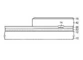
【0016】
図3は、本実施の形態による液晶表示パネルを対向基板側から見た構成を示している。図4は、ゲートバスライン12に沿って延びる図3のA−A線で切断した液晶表示パネルの断面構成を示している。図3及び図4に示すように、TFT基板2は、ガラス基板10上に形成されたゲートバスライン12を有している。ゲートバスライン12上の基板全面には、絶縁膜(ゲート絶縁膜)30が形成されている。絶縁膜30上には、ドレインバスライン14が形成されている。ドレインバスライン14上の基板全面には、保護膜(最終保護膜)34が形成されている。保護膜34上であって、シール剤40の形成される領域(シール剤形成領域)より内側の表示領域には、膜厚1〜3μm程度(例えば2.6μm)のアクリル系感光性樹脂からなるセルギャップ制御層42が形成されている。セルギャップ制御層42上には、例えばITO(Indium Tin Oxide)からなる画素電極16が画素領域毎に形成されている。
【0017】
対向基板4は、ガラス基板11上の表示領域に共通電極36を有している。なお、本実施の形態では、例えばフィールド順次方式によりカラー表示が行われる液晶表示装置を例に挙げているため、カラーフィルタ(CF;Color Filter)が形成されていない。CF方式でカラー表示が行われる液晶表示装置では、共通電極36の下層に赤色(R)、緑色(G)、青色(B)のCF層が、例えばTFT基板2側のドレインバスライン14に沿って延びるストライプ状に形成される。また、共通電極36の下層に、対向基板4側のセルギャップ制御層42を形成してもよい。
【0018】
TFT基板2と対向基板4とは、外周部に描画されたシール剤40を介して貼り合わされている。シール剤40の幅は、例えば1mm程度である。TFT基板2と対向基板4との間には、例えば強誘電性を有する液晶6が封止されている。対向基板4側から見ると、TFT基板2の隣接する2辺近傍の表面は露出している。TFT基板2の露出した領域のうち図3の左側には、ゲートバスライン12を駆動するドライバICが搭載された複数のTCP(Tape CarrierPackage)が実装される。また、TFT基板2の露出した領域のうち図3の下側には、ドレインバスライン14を駆動するドライバICが搭載された複数のTCPが実装される。
【0019】
シール剤40が形成された領域でのTFT基板2と対向基板4との間の間隔d2は、一般的な液晶表示装置と同様の3.5〜5.0μm程度(例えば4.0μm)である。これに対して、セルギャップ制御層42が形成された表示領域でのセルギャップd1は、間隔d2より狭くなっている(例えば1.4μm)。セルギャップd1は、球状スペーサや柱状スペーサ等のスペーサ(図4では図示せず)により維持されている。また、本実施の形態では、セルギャップd1がセルギャップ制御層42の膜厚よりも狭くなっている。
【0020】
本実施の形態では、シール剤40の形成された領域より内側の表示領域にセルギャップ制御層42が形成されている。このため、シール剤40の形成された領域での基板2、4間の間隔d2は比較的広くすることができ、表示領域でのセルギャップd1は比較的狭くすることができる。したがって、セルギャップd1の狭い液晶表示装置であっても、2枚の基板を貼り合わせる際のシール剤の広がり幅を狭くできるため、狭額縁化が可能になる。また、ディスペンサからのシール剤40の吐出量を少なくする必要がなく、シール破れによる液晶6の漏れが生じることがない。このため、液晶表示装置の製造歩留まりが向上する。
【0021】
また、比較的低温(−20〜−10℃程度)の環境下で液晶6が収縮しても、比較的硬度の低い樹脂で形成されたセルギャップ制御層42が変形することにより、液晶の体積変化に対応してパネル内の容積が変化し、パネル内に気泡が発生するのを防止できる。このため、強誘電性液晶を用いた液晶表示装置でも、液晶6の配向不良による表示異常を防止できる。したがって、良好な表示品質が得られる液晶表示装置を実現できる。
【0022】
次に、本実施の形態による液晶表示装置の製造方法について、図5乃至図7を用いて説明する。図5乃至図7は、本実施の形態による液晶表示装置のTFT基板の製造方法を示す工程断面図であり、図4に対応する断面を示している。まず、図5に示すように、ガラス基板10上の全面に金属層を成膜してパターニングし、ゲートバスライン(ゲート電極)12を形成する。同時に、蓄積容量バスライン18(図5では図示せず)が形成される。
【0023】
次に、ゲートバスライン12上の基板全面に、例えば窒化シリコン(SiN)/アモルファスシリコン(a−Si)/SiNを連続成膜し、絶縁膜30、a−Si層及びSiN膜を形成する。次に、SiN膜をパターニングして、チャネル保護膜(図示せず)を自己整合的に形成する。
【0024】
次に、チャネル保護膜上の基板全面に、例えばn+a−Si層と金属層とを成膜してパターニングし、ドレインバスライン14を形成する。同時に、TFT20のドレイン電極及びソース電極(共に図示せず)が形成される。これにより、TFT20が形成される。次に、ドレインバスライン14上の基板全面に、例えばSiNを成膜し、保護膜34を形成する。次に、保護膜34をパターニングして、ソース電極上にコンタクトホール(図示せず)を形成する。次に、保護膜34上の基板全面に、例えばアクリル系感光性樹脂を塗布し、感光性樹脂層42’を形成する。
【0025】
次に、図6に示すように、所定のフォトマスクを用いて露光して現像し、シール剤40が形成される領域及び当該領域より外側の感光性樹脂層42’を除去する。これにより、シール剤40が形成される領域より内側の表示領域にセルギャップ制御層42が形成される。
【0026】
次に、図7に示すように、セルギャップ制御層42上に例えばITOを成膜してパターニングし、画素電極16を画素領域毎に形成する。以上の工程を経てTFT基板2が完成する。その後、他の工程を経て形成された対向基板4とTFT基板2のいずれか一方の外周部にシール剤を塗布形成して両基板2、4を貼り合わせ、両基板2、4間に例えば強誘電性を有する液晶を封止して、図3及び図4に示す液晶表示装置が完成する。
【0027】
本実施の形態によれば、セルギャップ制御層42を感光性樹脂により形成しているため、図3及び図4に示す液晶表示装置を容易に製造できる。
【0028】
以下、本実施の形態による液晶表示装置の具体的構成について、実施例1乃至4を用いて説明する。
【0029】
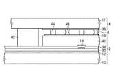
(実施例1)
まず、本実施の形態の実施例1による液晶表示装置について図8を用いて説明する。図8は、本実施例による液晶表示装置の要部構成を示す断面図であり、図4に対応する断面を示している。図8に示すように、TFT基板2のガラス基板10上には、ゲートバスライン12が形成されている。ゲートバスライン12上の基板全面には、絶縁膜30が形成されている。絶縁膜30上には、ドレインバスライン14が形成されている。ドレインバスライン14上の基板全面には、保護膜34が形成されている。保護膜34上であって、シール剤40の形成される領域より内側の表示領域には、例えば膜厚2.6μmのアクリル系感光性樹脂からなるセルギャップ制御層42が形成されている。セルギャップ制御層42上には、例えばITOからなる画素電極16が画素領域毎に形成されている。対向基板4は、ガラス基板11上の表示領域に共通電極36を有している。
【0030】
TFT基板2と対向基板4とは、外周部に描画されたシール剤40を介して貼り合わされている。シール剤40の幅は、例えば1mm程度である。TFT基板2と対向基板4との間には、例えば強誘電性を有する液晶6が封止されている。
【0031】
また、液晶表示装置は、セルギャップを維持する球状スペーサ46を有している。セルギャップは、球状スペーサ46の粒径(例えば1.4μm)によって決定される。一般に、TNモード等の液晶表示装置には樹脂製などの球状スペーサ46が用いられる。また、強誘電性液晶を用いた液晶表示装置には、硬度が高く、粒径を高精度に制御可能なシリカ製などの球状スペーサ46が用いられる。
【0032】
本実施例では、シール剤40の形成された領域より内側の表示領域にセルギャップ制御層42が形成されている。このため、シール剤40の形成された領域での基板2、4間の間隔は比較的広くすることができ、表示領域でのセルギャップは比較的狭くすることができる。したがって、セルギャップの狭い液晶表示装置であっても、2枚の基板を貼り合わせる際のシール剤の広がり幅を狭くできるため、狭額縁化が可能になる。また、ディスペンサからのシール剤40の吐出量を少なくする必要がなく、シール破れによる液晶6の漏れが生じることがない。このため、液晶表示装置の製造歩留まりが向上する。
【0033】
また、比較的低温の環境下で液晶6が収縮しても、比較的硬度の低い樹脂で形成されたセルギャップ制御層42が変形することにより、液晶の体積変化に対応してパネル内の容積が変化し、パネル内に気泡が発生するのを防止できる。このため、強誘電性液晶を用いた液晶表示装置でも、液晶6の配向不良による表示異常を防止できる。したがって、良好な表示品質が得られる液晶表示装置を実現できる。
【0034】
(実施例2)
次に、本実施の形態の実施例2による液晶表示装置について図9を用いて説明する。図9は、本実施例による液晶表示装置の要部構成を示す断面図であり、図4に対応する断面を示している。図9に示すように、TFT基板2のガラス基板10上には、ゲートバスライン12が形成されている。ゲートバスライン12上の基板全面には、絶縁膜30が形成されている。絶縁膜30上には、ドレインバスライン14が形成されている。ドレインバスライン14上の基板全面には、保護膜34が形成されている。保護膜34上であって、シール剤40の形成される領域より内側の表示領域には、例えば膜厚2.6μmのアクリル系感光性樹脂からなるセルギャップ制御層42が形成されている。セルギャップ制御層42上には、例えばITOからなる画素電極16が画素領域毎に形成されている。対向基板4は、ガラス基板11上の表示領域に共通電極36を有している。
【0035】
TFT基板2と対向基板4とは、外周部に描画されたシール剤40を介して貼り合わされている。シール剤40の幅は、例えば1mm程度である。TFT基板2と対向基板4との間には、例えば強誘電性を有する液晶6が封止されている。
【0036】
また、液晶表示装置は、セルギャップを維持する柱状スペーサ44を有している。セルギャップは、柱状スペーサ44の高さ(例えば1.4μm)によって決定される。柱状スペーサ44は、アクリル系やノボラック系などの樹脂からなり、フォトリソグラフィ法を用いてパターニングされる。柱状スペーサ44は、球状スペーサ46と異なり、バスライン12、14の交点上や、ゲートバスライン12上の全域などの任意の位置に任意の形状及び配置密度で形成できる特徴を有している。本実施例によれば、実施例1と同様の効果が得られる。
【0037】
(実施例3)
次に、本実施の形態の実施例3による液晶表示装置について図10を用いて説明する。図10は、本実施例による液晶表示装置の要部構成を示す断面図であり、図4に対応する断面を示している。図10に示すように、TFT基板2のガラス基板10上には、ゲートバスライン12が形成されている。ゲートバスライン12上の基板全面には、絶縁膜30が形成されている。絶縁膜30上には、ドレインバスライン14が形成されている。ドレインバスライン14上の基板全面には、保護膜34が形成されている。保護膜34上であって、シール剤40の形成される領域より内側の表示領域には、例えば膜厚2.6μmのアクリル系感光性樹脂からなるセルギャップ制御層42が形成されている。セルギャップ制御層42上には、例えばITOからなる画素電極16が画素領域毎に形成されている。対向基板4は、ガラス基板11上の表示領域に共通電極36を有している。
【0038】
TFT基板2と対向基板4とは、外周部に描画されたシール剤40を介して貼り合わされている。シール剤40の幅は、例えば1mm程度である。TFT基板2と対向基板4との間には、例えば強誘電性を有する液晶6が封止されている。
【0039】
また、液晶表示装置は、セルギャップを維持する球状スペーサ46と、両基板2、4を互いに強固に固定する接着剤48とを有している。接着剤48は、例えばエポキシ系の熱硬化型樹脂であり、硬化前は粒径2〜6μm程度の粒子状である。接着剤48は、球状スペーサ46の散布と同時あるいは別々に、基板2、4のいずれか一方に散布される。その後、両基板2、4を貼り合わせ、加圧しながら約200℃程度まで加熱して、所定のセルギャップを維持しつつ接着剤48を硬化させる。
【0040】
一般に、ある領域の基板面に外部から圧力が加えられると、当該領域の液晶6が他の領域に移動する。このため、当該領域ではセルギャップが狭くなるとともに、他の領域ではセルギャップが広くなる。しかし、本実施例では、接着剤48により両基板2、4が互いに強固に固定され、セルギャップが広がることがないため、ある領域の基板面に外側から圧力が加えられても当該領域のセルギャップが狭くなることがない。したがって、本実施例によれば、実施例1と同様の効果が得られるとともに、セルギャップの変動が生じ難く、強誘電性液晶を用いた液晶表示装置の表示異常を防止できる。
【0041】
(実施例4)
次に、本実施の形態の実施例4による液晶表示装置について図11を用いて説明する。図11は、本実施例による液晶表示装置の要部構成を示す断面図であり、図4に対応する断面を示している。図11に示すように、TFT基板2のガラス基板10上には、ゲートバスライン12が形成されている。ゲートバスライン12上の基板全面には、絶縁膜30が形成されている。絶縁膜30上には、ドレインバスライン14が形成されている。ドレインバスライン14上の基板全面には、保護膜34が形成されている。保護膜34上であって、シール剤40の形成される領域より内側の表示領域には、例えば膜厚2.6μmのアクリル系感光性樹脂からなるセルギャップ制御層42が形成されている。セルギャップ制御層42上には、例えばITOからなる画素電極16が画素領域毎に形成されている。対向基板4は、ガラス基板11上の表示領域に共通電極36を有している。
【0042】
TFT基板2と対向基板4とは、外周部に描画されたシール剤40を介して貼り合わされている。シール剤40の幅は、例えば1mm程度である。TFT基板2と対向基板4との間には、例えば強誘電性を有する液晶6が封止されている。
【0043】
また、液晶表示装置は、セルギャップを維持する柱状スペーサ44と、両基板2、4を互いに強固に固定する接着剤48とを有している。接着剤48は、例えばエポキシ系の熱硬化型樹脂であり、硬化前は粒径2〜6μm程度の粒子状である。接着剤48は、貼合せ工程の前に基板2、4のいずれか一方に散布される。その後、両基板2、4を貼り合わせ、加圧しながら約200℃程度まで加熱して、所定のセルギャップを維持しつつ接着剤48を硬化させる。本実施例によれば、実施例3と同様の効果が得られる。
【0044】
以上説明したように、本実施の形態によれば、セルギャップの極端に狭い液晶表示装置においても、従来とほぼ同様の製造方法を用いることができる。また、本実施の形態の実施例3及び4によれば、強誘電性液晶のように外圧に対して極めてデリケートな液晶材料を用いても、表示品質に悪影響を及ぼさず、外部からの圧力に対して強固な液晶表示装置を実現できる。
【0045】
本発明は、上記実施の形態に限らず種々の変形が可能である。
例えば、上記実施の形態では強誘電性液晶を用いた液晶表示装置を例に挙げたが、本発明はこれに限らず、ネマティック液晶を用いたTNモード等の他の液晶表示装置にも適用できる。
【0046】
また、上記実施の形態では透過型の液晶表示装置を例に挙げたが、本発明はこれに限らず、反射型や半透過型等の他の液晶表示装置にも適用できる。
【0047】
上記実施の形態ではアクティブマトリクス型の液晶表示装置を例に挙げたが、本発明はこれに限らず、単純マトリクス型の液晶表示装置にも適用できる。
【0048】
以上説明した実施の形態による液晶表示装置用基板及びそれを備えた液晶表示装置は、以下のようにまとめられる。
(付記1)
基板の外周部に配置され、シール剤が形成されるシール剤形成領域と、
前記シール剤形成領域よりも内側に形成され、前記基板に対向配置される対向基板との間のセルギャップを制御するセルギャップ制御層と
を有することを特徴とする液晶表示装置用基板。
【0049】
(付記2)
付記1記載の液晶表示装置用基板において、
前記セルギャップ制御層は、感光性樹脂により形成されていること
を特徴とする液晶表示装置用基板。
【0050】
(付記3)
一対の基板と、前記基板間に封止された液晶とを有する液晶表示装置であって、
前記基板の一方に、付記1又は2に記載の液晶表示装置用基板が用いられていること
を特徴とする液晶表示装置。
【0051】
(付記4)
付記3記載の液晶表示装置において、
一方の前記基板上に散布され、前記一対の基板を互いに固定する接着剤をさらに有していること
を特徴とする液晶表示装置。
【0052】
(付記5)
付記3又は4に記載の液晶表示装置において、
前記セルギャップを維持する柱状スペーサをさらに有していること
を特徴とする液晶表示装置。
【0053】
(付記6)
付記3又は4に記載の液晶表示装置において、
前記セルギャップを維持する球状スペーサをさらに有していること
を特徴とする液晶表示装置。
【0054】
(付記7)
付記3乃至6のいずれか1項に記載の液晶表示装置において、
前記セルギャップ制御層は、前記セルギャップより厚い膜厚を有していること
を特徴とする液晶表示装置。
【0055】
【発明の効果】
以上の通り、本発明によれば、製造歩留まりが向上し、良好な表示品質の得られる液晶表示装置を実現できる。
【図面の簡単な説明】
【図1】本発明の一実施の形態による液晶表示装置の概略構成を示す図である。
【図2】本発明の一実施の形態による液晶表示装置のTFT基板の等価回路を示す図である。
【図3】本発明の一実施の形態による液晶表示装置の液晶表示パネルの構成を示す図である。
【図4】本発明の一実施の形態による液晶表示装置の液晶表示パネルの要部構成を示す断面図である。
【図5】本発明の一実施の形態による液晶表示装置のTFT基板の製造方法を示す工程断面図である。
【図6】本発明の一実施の形態による液晶表示装置のTFT基板の製造方法を示す工程断面図である。
【図7】本発明の一実施の形態による液晶表示装置のTFT基板の製造方法を示す工程断面図である。
【図8】本発明の一実施の形態の実施例1による液晶表示装置の要部構成を示す断面図である。
【図9】本発明の一実施の形態の実施例2による液晶表示装置の要部構成を示す断面図である。
【図10】本発明の一実施の形態の実施例3による液晶表示装置の要部構成を示す断面図である。
【図11】本発明の一実施の形態の実施例4による液晶表示装置の要部構成を示す断面図である。
【符号の説明】
2 TFT基板
4 対向基板
10、11 ガラス基板
12 ゲートバスライン
14 ドレインバスライン
16 画素電極
18 蓄積容量バスライン
20 TFT
30 絶縁膜
34 保護膜
36 共通電極
40 シール剤
42 セルギャップ制御層
42’ 感光性樹脂層
44 柱状スペーサ
46 球状スペーサ
48 接着剤
80 ゲートバスライン駆動回路
82 ドレインバスライン駆動回路
84 制御回路
86、87 偏光板
88 バックライトユニット[0001]
TECHNICAL FIELD OF THE INVENTION
The present invention relates to a liquid crystal display device used for a display unit or the like of an electronic device and a substrate for a liquid crystal display device used therefor, and more particularly to a liquid crystal display device having a relatively narrow cell gap and a substrate for a liquid crystal display device used therefor.
[0002]
[Prior art]
The liquid crystal display device has two substrates bonded together via a sealant applied to an outer peripheral portion, and a liquid crystal sealed between the two substrates. Further, the liquid crystal display device has a spherical spacer or a columnar spacer in order to maintain a predetermined cell gap.
[0003]
The spherical spacer is made of plastic beads or the like having substantially the same particle size. The spherical spacers are scattered on one of the substrates using a wet scatter method or a dry scatter method before the laminating step of laminating the two substrates, and are dispersed in the panel. On the other hand, the columnar spacer is made of a photosensitive resin or the like, and is formed at an arbitrary position and an arbitrary density on one substrate using a photolithography method or the like.
[0004]
The sealant is formed by drawing using a dispenser. As a method for ensuring the seal, there is known a technique of removing a flattening film made of an acrylic resin in a part of a region where a sealant is formed (for example, see Patent Document 1).
[0005]
Further, as a method of realizing a relatively narrow cell gap, a stripe pattern of a heat-fusible material is formed on each of the opposing surfaces of the two substrates, and the two substrates are overlapped so that the stripe pattern becomes a lattice shape. A matching technique is known (for example, see Patent Document 2).
[0006]
[Patent Document 1]
JP 2001-337334 A [Patent Document 2]
JP-A-57-70521 [Patent Document 3]
JP-A-4-320473
[Problems to be solved by the invention]
For example, in a liquid crystal display device using a ferroelectric liquid crystal, it is necessary to narrow the cell gap to about 1.0 to 1.5 μm. In the configurations described in
[0008]
In the case of a liquid crystal display device using a ferroelectric liquid crystal, disturbance of the alignment of the liquid crystal due to disturbance is fatal, and a display abnormality caused by the disturbance of the alignment of the liquid crystal cannot be recovered as it is. For example, if the cell gap fluctuates due to the pressure applied to the display screen from the outside, the alignment of the liquid crystal is disturbed, and a display abnormality (display unevenness) that cannot be recovered as it is is visually recognized.
[0009]
In particular, when a spherical spacer is used as the spacer, it is difficult to uniformly disperse the spherical spacer over the entire surface of the substrate. In a liquid crystal display device in which spherical spacers are not uniformly distributed in a panel, the cell gap is likely to fluctuate when the substrate surface is pressed from the outside.
[0010]
Furthermore, in an environment of relatively low temperature (about -20 to -10 ° C.), a change in volume in the panel is small with respect to a change in volume due to contraction of the liquid crystal, so that bubbles are generated in the panel. When bubbles are generated, the orientation of the liquid crystal is disturbed. Therefore, in a liquid crystal display device using a ferroelectric liquid crystal, there is a problem that a display abnormality that cannot be recovered as it is is visually recognized.
[0011]
SUMMARY OF THE INVENTION An object of the present invention is to provide a liquid crystal display device having an improved production yield and good display quality, and a substrate for a liquid crystal display device used therefor.
[0012]
[Means for Solving the Problems]
The above object is achieved by providing a cell between a sealant forming region in which a sealant is formed, which is arranged on an outer peripheral portion of a substrate, and a counter substrate, which is formed inside the sealant forming region and is arranged to face the substrate. A liquid crystal display substrate having a cell gap control layer for controlling a gap.
[0013]
BEST MODE FOR CARRYING OUT THE INVENTION
A substrate for a liquid crystal display device and a liquid crystal display device including the same according to an embodiment of the present invention will be described with reference to FIGS. FIG. 1 shows a schematic configuration of the liquid crystal display device according to the present embodiment. As shown in FIG. 1, in a liquid crystal display device, a
[0014]
FIG. 2 shows an equivalent circuit of an element formed on the
[0015]
Returning to FIG. 1, on the
[0016]
FIG. 3 shows a configuration of the liquid crystal display panel according to the present embodiment as viewed from the counter substrate side. FIG. 4 shows a cross-sectional configuration of the liquid crystal display panel taken along line AA in FIG. 3 extending along the
[0017]
The
[0018]
The
[0019]
The distance d2 between the
[0020]
In the present embodiment, the cell
[0021]
Further, even if the
[0022]
Next, a method for manufacturing the liquid crystal display device according to the present embodiment will be described with reference to FIGS. 5 to 7 are process cross-sectional views showing a method for manufacturing the TFT substrate of the liquid crystal display device according to the present embodiment, and show cross sections corresponding to FIG. First, as shown in FIG. 5, a metal layer is formed on the entire surface of the
[0023]
Next, over the entire surface of the substrate on the
[0024]
Next, for example, an n+ a-Si layer and a metal layer are formed and patterned on the entire surface of the substrate on the channel protective film to form a
[0025]
Next, as shown in FIG. 6, exposure is performed using a predetermined photomask and development is performed to remove the region where the
[0026]
Next, as shown in FIG. 7, for example, an ITO film is formed on the cell
[0027]
According to the present embodiment, since the cell
[0028]
Hereinafter, a specific configuration of the liquid crystal display device according to the present embodiment will be described using Examples 1 to 4.
[0029]
(Example 1)
First, a liquid crystal display device according to Example 1 of the present embodiment will be described with reference to FIG. FIG. 8 is a cross-sectional view showing a main part configuration of the liquid crystal display device according to the present embodiment, and shows a cross section corresponding to FIG. As shown in FIG. 8, a
[0030]
The
[0031]
Further, the liquid crystal display device has a
[0032]
In this embodiment, the cell
[0033]
Also, even if the
[0034]
(Example 2)
Next, a liquid crystal display device according to a second embodiment of the present embodiment will be described with reference to FIG. FIG. 9 is a cross-sectional view showing a main part configuration of the liquid crystal display device according to the present embodiment, and shows a cross section corresponding to FIG. As shown in FIG. 9, a
[0035]
The
[0036]
Further, the liquid crystal display device has a
[0037]
(Example 3)
Next, a liquid crystal display device according to a third embodiment of the present embodiment will be described with reference to FIG. FIG. 10 is a cross-sectional view showing a main part configuration of the liquid crystal display device according to the present embodiment, and shows a cross section corresponding to FIG. As shown in FIG. 10, a
[0038]
The
[0039]
Further, the liquid crystal display device has a
[0040]
Generally, when pressure is externally applied to the substrate surface in a certain area, the
[0041]
(Example 4)
Next, a liquid crystal display device according to Example 4 of the present embodiment will be described with reference to FIG. FIG. 11 is a cross-sectional view showing a main part configuration of the liquid crystal display device according to the present embodiment, and shows a cross section corresponding to FIG. As shown in FIG. 11, a
[0042]
The
[0043]
Further, the liquid crystal display device has a
[0044]
As described above, according to the present embodiment, even in a liquid crystal display device having an extremely narrow cell gap, it is possible to use substantially the same manufacturing method as in the related art. Further, according to Examples 3 and 4 of the present embodiment, even if a liquid crystal material which is extremely sensitive to an external pressure such as a ferroelectric liquid crystal is used, the display quality is not adversely affected and the external pressure is not affected. On the other hand, a strong liquid crystal display device can be realized.
[0045]
The present invention is not limited to the above embodiment, and various modifications are possible.
For example, in the above embodiment, a liquid crystal display device using a ferroelectric liquid crystal is taken as an example, but the present invention is not limited to this, and can be applied to other liquid crystal display devices such as a TN mode using a nematic liquid crystal. .
[0046]
In the above embodiment, a transmissive liquid crystal display device is described as an example. However, the present invention is not limited to this, and can be applied to other liquid crystal display devices such as a reflective liquid crystal display device and a transflective liquid crystal display device.
[0047]
In the above embodiment, an active matrix type liquid crystal display device has been described as an example, but the present invention is not limited to this, and can be applied to a simple matrix type liquid crystal display device.
[0048]
The substrate for a liquid crystal display device according to the embodiment described above and the liquid crystal display device including the same are summarized as follows.
(Appendix 1)
A sealant forming region arranged on the outer peripheral portion of the substrate and in which a sealant is formed;
A substrate for a liquid crystal display device, comprising: a cell gap control layer that is formed inside the sealant formation region and controls a cell gap between the substrate and a counter substrate that is disposed to face the substrate.
[0049]
(Appendix 2)
The substrate for a liquid crystal display device according to Supplementary Note 1,
The substrate for a liquid crystal display device, wherein the cell gap control layer is formed of a photosensitive resin.
[0050]
(Appendix 3)
A liquid crystal display device having a pair of substrates and a liquid crystal sealed between the substrates,
3. A liquid crystal display device, wherein the substrate for a liquid crystal display device according to
[0051]
(Appendix 4)
The liquid crystal display device according to claim 3, wherein
A liquid crystal display device further comprising an adhesive dispersed on one of the substrates and fixing the pair of substrates to each other.
[0052]
(Appendix 5)
The liquid crystal display device according to
A liquid crystal display device further comprising a columnar spacer for maintaining the cell gap.
[0053]
(Appendix 6)
The liquid crystal display device according to
A liquid crystal display device further comprising a spherical spacer for maintaining the cell gap.
[0054]
(Appendix 7)
7. The liquid crystal display device according to any one of supplementary notes 3 to 6, wherein
The liquid crystal display device, wherein the cell gap control layer has a thickness greater than the cell gap.
[0055]
【The invention's effect】
As described above, according to the present invention, it is possible to realize a liquid crystal display device having an improved manufacturing yield and good display quality.
[Brief description of the drawings]
FIG. 1 is a diagram showing a schematic configuration of a liquid crystal display device according to an embodiment of the present invention.
FIG. 2 is a diagram showing an equivalent circuit of a TFT substrate of the liquid crystal display according to one embodiment of the present invention.
FIG. 3 is a diagram showing a configuration of a liquid crystal display panel of the liquid crystal display device according to one embodiment of the present invention.
FIG. 4 is a cross-sectional view showing a main configuration of a liquid crystal display panel of the liquid crystal display device according to the embodiment of the present invention.
FIG. 5 is a process sectional view illustrating the method for manufacturing the TFT substrate of the liquid crystal display device according to the embodiment of the present invention.
FIG. 6 is a process sectional view illustrating the method for manufacturing the TFT substrate of the liquid crystal display device according to the embodiment of the present invention.
FIG. 7 is a process sectional view illustrating the method for manufacturing the TFT substrate of the liquid crystal display device according to the embodiment of the present invention.
FIG. 8 is a cross-sectional view illustrating a configuration of a main part of a liquid crystal display device according to Example 1 of one embodiment of the present invention.
FIG. 9 is a cross-sectional view illustrating a configuration of a main part of a liquid crystal display device according to Example 2 of one embodiment of the present invention.
FIG. 10 is a cross-sectional view illustrating a configuration of a main part of a liquid crystal display device according to Example 3 of one embodiment of the present invention.
FIG. 11 is a cross-sectional view illustrating a configuration of a main part of a liquid crystal display device according to Example 4 of one embodiment of the present invention.
[Explanation of symbols]
2
REFERENCE SIGNS
Claims (5)
Translated fromJapanese前記シール剤形成領域よりも内側に形成され、前記基板に対向配置される対向基板との間のセルギャップを制御するセルギャップ制御層と
を有することを特徴とする液晶表示装置用基板。A sealant forming region arranged on the outer peripheral portion of the substrate and in which a sealant is formed;
A substrate for a liquid crystal display device, comprising: a cell gap control layer that is formed inside the sealant formation region and controls a cell gap between the substrate and a counter substrate that is disposed to face the substrate.
前記セルギャップ制御層は、感光性樹脂により形成されていること
を特徴とする液晶表示装置用基板。The liquid crystal display device substrate according to claim 1,
The substrate for a liquid crystal display device, wherein the cell gap control layer is formed of a photosensitive resin.
前記基板の一方に、請求項1又は2に記載の液晶表示装置用基板が用いられていること
を特徴とする液晶表示装置。A liquid crystal display device having a pair of substrates and a liquid crystal sealed between the substrates,
A liquid crystal display device, wherein the substrate for a liquid crystal display device according to claim 1 is used as one of the substrates.
一方の前記基板上に散布され、前記一対の基板を互いに固定する接着剤をさらに有していること
を特徴とする液晶表示装置。The liquid crystal display device according to claim 3,
A liquid crystal display device further comprising an adhesive dispersed on one of the substrates and fixing the pair of substrates to each other.
前記セルギャップ制御層は、前記セルギャップより厚い膜厚を有していること
を特徴とする液晶表示装置。The liquid crystal display device according to claim 3, wherein
The liquid crystal display device, wherein the cell gap control layer has a thickness greater than the cell gap.
Priority Applications (2)
| Application Number | Priority Date | Filing Date | Title |
|---|---|---|---|
| JP2002364665AJP2004198567A (en) | 2002-12-17 | 2002-12-17 | Liquid crystal display device substrate and liquid crystal display device having the same |
| US10/737,182US20040156007A1 (en) | 2002-12-17 | 2003-12-16 | Substrate for liquid crystal display and liquid crystal display having the same |
Applications Claiming Priority (1)
| Application Number | Priority Date | Filing Date | Title |
|---|---|---|---|
| JP2002364665AJP2004198567A (en) | 2002-12-17 | 2002-12-17 | Liquid crystal display device substrate and liquid crystal display device having the same |
Publications (1)
| Publication Number | Publication Date |
|---|---|
| JP2004198567Atrue JP2004198567A (en) | 2004-07-15 |
Family
ID=32762419
Family Applications (1)
| Application Number | Title | Priority Date | Filing Date |
|---|---|---|---|
| JP2002364665APendingJP2004198567A (en) | 2002-12-17 | 2002-12-17 | Liquid crystal display device substrate and liquid crystal display device having the same |
Country Status (2)
| Country | Link |
|---|---|
| US (1) | US20040156007A1 (en) |
| JP (1) | JP2004198567A (en) |
Families Citing this family (2)
| Publication number | Priority date | Publication date | Assignee | Title |
|---|---|---|---|---|
| KR20050008040A (en)* | 2003-07-14 | 2005-01-21 | 삼성에스디아이 주식회사 | Field-sequential liquid crystal display panel wherein storage capacitor is formed using scan electrode line |
| JPWO2007029334A1 (en)* | 2005-09-09 | 2009-03-26 | 富士通株式会社 | Liquid crystal display |
Family Cites Families (9)
| Publication number | Priority date | Publication date | Assignee | Title |
|---|---|---|---|---|
| JPS6262334A (en)* | 1985-09-13 | 1987-03-19 | Canon Inc | Liquid crystal element |
| JP2782291B2 (en)* | 1990-08-30 | 1998-07-30 | キヤノン株式会社 | Ferroelectric liquid crystal color panel |
| JP3014291B2 (en)* | 1995-03-10 | 2000-02-28 | インターナショナル・ビジネス・マシーンズ・コーポレイション | Liquid crystal display panel, liquid crystal display device, and method of manufacturing liquid crystal display panel |
| JP3272212B2 (en)* | 1995-09-29 | 2002-04-08 | シャープ株式会社 | Transmissive liquid crystal display device and method of manufacturing the same |
| DE19712233C2 (en)* | 1996-03-26 | 2003-12-11 | Lg Philips Lcd Co | Liquid crystal display and manufacturing method therefor |
| JP3883641B2 (en)* | 1997-03-27 | 2007-02-21 | 株式会社半導体エネルギー研究所 | Contact structure and active matrix display device |
| US6181397B1 (en)* | 1997-04-01 | 2001-01-30 | Dai Nippon Printing Co., Ltd. | Reflection-type liquid crystal display panel and method of fabricating the same |
| KR100277309B1 (en)* | 1997-06-13 | 2001-01-15 | 마찌다 가쯔히꼬 | Liquid Crystal Display and Manufacturing Method Thereof |
| JP2000047189A (en)* | 1998-07-28 | 2000-02-18 | Sharp Corp | Liquid crystal display device |
- 2002
- 2002-12-17JPJP2002364665Apatent/JP2004198567A/enactivePending
- 2003
- 2003-12-16USUS10/737,182patent/US20040156007A1/ennot_activeAbandoned
Also Published As
| Publication number | Publication date |
|---|---|
| US20040156007A1 (en) | 2004-08-12 |
Similar Documents
| Publication | Publication Date | Title |
|---|---|---|
| US7812916B2 (en) | Liquid crystal display panel with spherical spacer and a concave portion opposite to the spacer | |
| US7518695B2 (en) | Liquid crystal display device, method for manufacturing the same and spacer structure | |
| CN1989443B (en) | Color filter substrate and liquid crystal display panel including the color filter substrate | |
| JP4177658B2 (en) | Liquid crystal display | |
| CN1991530B (en) | Display panel and method of manufacturing the same | |
| TWI519873B (en) | Liquid crystal display device and manufacturing method thereof | |
| KR101031166B1 (en) | Liquid crystal display panel | |
| US7463327B2 (en) | Liquid crystal display | |
| JP2005242310A (en) | Liquid crystal display device and manufacturing method thereof | |
| US20030081155A1 (en) | Method of fabricating liquid crystal display device | |
| JPH10268361A (en) | Liquid crystal display device and its manufacture | |
| JP2005309239A (en) | Liquid crystal display | |
| JP2017102276A (en) | Curved display device | |
| KR100763169B1 (en) | Substrate suction vacuum chuck structure | |
| KR20050001942A (en) | Mother glass substrate for liquid crystal display device | |
| KR20080062826A (en) | Liquid crystal display | |
| KR101681923B1 (en) | Liquid Crystal Display Device and Method for fabricating the same | |
| WO2010079540A1 (en) | Liquid-crystal display panel | |
| KR100603669B1 (en) | LCD and its manufacturing method | |
| JP2004198567A (en) | Liquid crystal display device substrate and liquid crystal display device having the same | |
| JP2004145084A (en) | Liquid crystal panel and manufacturing method thereof | |
| JP2001324720A (en) | Liquid crystal display device and its manufacturing method | |
| KR20040011671A (en) | Liquid Crystal Display Device | |
| JP6671182B2 (en) | Liquid crystal display panel manufacturing method | |
| JP5026883B2 (en) | Electro-optical device and electronic apparatus |
Legal Events
| Date | Code | Title | Description |
|---|---|---|---|
| A711 | Notification of change in applicant | Free format text:JAPANESE INTERMEDIATE CODE: A711 Effective date:20050712 | |
| A711 | Notification of change in applicant | Free format text:JAPANESE INTERMEDIATE CODE: A711 Effective date:20050713 | |
| RD02 | Notification of acceptance of power of attorney | Free format text:JAPANESE INTERMEDIATE CODE: A7422 Effective date:20050722 | |
| A621 | Written request for application examination | Free format text:JAPANESE INTERMEDIATE CODE: A621 Effective date:20050907 | |
| A977 | Report on retrieval | Free format text:JAPANESE INTERMEDIATE CODE: A971007 Effective date:20071005 | |
| A131 | Notification of reasons for refusal | Free format text:JAPANESE INTERMEDIATE CODE: A131 Effective date:20080610 | |
| A02 | Decision of refusal | Free format text:JAPANESE INTERMEDIATE CODE: A02 Effective date:20081104 |