JP2004178895A - Organic electroluminescence element and display device - Google Patents
Organic electroluminescence element and display deviceDownload PDFInfo
- Publication number
- JP2004178895A JP2004178895AJP2002342192AJP2002342192AJP2004178895AJP 2004178895 AJP2004178895 AJP 2004178895AJP 2002342192 AJP2002342192 AJP 2002342192AJP 2002342192 AJP2002342192 AJP 2002342192AJP 2004178895 AJP2004178895 AJP 2004178895A
- Authority
- JP
- Japan
- Prior art keywords
- group
- organic
- compound
- light
- general formula
- Prior art date
- Legal status (The legal status is an assumption and is not a legal conclusion. Google has not performed a legal analysis and makes no representation as to the accuracy of the status listed.)
- Granted
Links
- 0CCC(C)(c1cc(-c2ccccc2*2c3cc(*4c5ccccc5-c5c4cccc5)cc(*4c(cccc5)c5-c5c4cccc5)c3)c2cc1)c1ccc(*(c2c-3cccc2)c2cc(*4c(ccc(C(C)(CCC=C)c5ccc(*(c6c-7cccc6)c6cc(*8c9ccccc9-c9c8cccc9)cc(*8c9ccccc9-c9c8cccc9)c6)c-7c5)c5)c5-c5c4cccc5)cc(*4c5ccccc5-c5c4cccc5)c2)c-3c1Chemical compoundCCC(C)(c1cc(-c2ccccc2*2c3cc(*4c5ccccc5-c5c4cccc5)cc(*4c(cccc5)c5-c5c4cccc5)c3)c2cc1)c1ccc(*(c2c-3cccc2)c2cc(*4c(ccc(C(C)(CCC=C)c5ccc(*(c6c-7cccc6)c6cc(*8c9ccccc9-c9c8cccc9)cc(*8c9ccccc9-c9c8cccc9)c6)c-7c5)c5)c5-c5c4cccc5)cc(*4c5ccccc5-c5c4cccc5)c2)c-3c10.000description3
- JLJVDKSUDSOPRB-UHFFFAOYSA-NCCCCC(C)(c(cc1)cc(c2ccccc22)c1[n]2-c1cc(-[n]2c(cccc3)c3c3c2cccc3)cc(-[n]2c(cccc3)c3c3c2cccc3)c1)c(cc1c2c3cccc2)ccc1[n]3-c1cc(-[n]2c3ccc(C(CC)(CCCC)c(cc4c5c6cccc5)ccc4[n]6-c4cc(-[n]5c6ccccc6c6c5cccc6)cc(-[n]5c(cccc6)c6c6c5cccc6)c4)cc3c3c2cccc3)cc(-[n]2c3ccccc3c3c2cccc3)c1Chemical compoundCCCCC(C)(c(cc1)cc(c2ccccc22)c1[n]2-c1cc(-[n]2c(cccc3)c3c3c2cccc3)cc(-[n]2c(cccc3)c3c3c2cccc3)c1)c(cc1c2c3cccc2)ccc1[n]3-c1cc(-[n]2c3ccc(C(CC)(CCCC)c(cc4c5c6cccc5)ccc4[n]6-c4cc(-[n]5c6ccccc6c6c5cccc6)cc(-[n]5c(cccc6)c6c6c5cccc6)c4)cc3c3c2cccc3)cc(-[n]2c3ccccc3c3c2cccc3)c1JLJVDKSUDSOPRB-UHFFFAOYSA-N0.000description1
- CYYPKJQCGJWFMJ-UHFFFAOYSA-NCC[n](c(ccc(C)c1)c1c1c2)c1ccc2-c1cc(-c(cc2)cc(c3c4)c2[n](CC)c3ccc4-c2ccc3[n](CC)c(ccc(-c4cc(-c(cc5)cc6c5[n](CC)c5c6cc(C)cc5)cc(-c5ccc6[n](CC)c(ccc(C)c7)c7c6c5)c4)c4)c4c3c2)cc(-c2ccc3[n](CC)c(ccc(C)c4)c4c3c2)c1Chemical compoundCC[n](c(ccc(C)c1)c1c1c2)c1ccc2-c1cc(-c(cc2)cc(c3c4)c2[n](CC)c3ccc4-c2ccc3[n](CC)c(ccc(-c4cc(-c(cc5)cc6c5[n](CC)c5c6cc(C)cc5)cc(-c5ccc6[n](CC)c(ccc(C)c7)c7c6c5)c4)c4)c4c3c2)cc(-c2ccc3[n](CC)c(ccc(C)c4)c4c3c2)c1CYYPKJQCGJWFMJ-UHFFFAOYSA-N0.000description1
- UJNWQYKCQANLJV-UHFFFAOYSA-NCN(c(cc1)ccc1-[n]1c(cccc2)c2c2c1cccc2)c1cc(-c(cc2)ccc2-[n]2c3ccccc3c3c2cccc3)cc(-c(cc2)ccc2-[n]2c3ccccc3c3c2cccc3)c1Chemical compoundCN(c(cc1)ccc1-[n]1c(cccc2)c2c2c1cccc2)c1cc(-c(cc2)ccc2-[n]2c3ccccc3c3c2cccc3)cc(-c(cc2)ccc2-[n]2c3ccccc3c3c2cccc3)c1UJNWQYKCQANLJV-UHFFFAOYSA-N0.000description1
Images


Classifications
- H—ELECTRICITY
- H05—ELECTRIC TECHNIQUES NOT OTHERWISE PROVIDED FOR
- H05B—ELECTRIC HEATING; ELECTRIC LIGHT SOURCES NOT OTHERWISE PROVIDED FOR; CIRCUIT ARRANGEMENTS FOR ELECTRIC LIGHT SOURCES, IN GENERAL
- H05B33/00—Electroluminescent light sources
- H05B33/12—Light sources with substantially two-dimensional radiating surfaces
- H05B33/14—Light sources with substantially two-dimensional radiating surfaces characterised by the chemical or physical composition or the arrangement of the electroluminescent material, or by the simultaneous addition of the electroluminescent material in or onto the light source
- C—CHEMISTRY; METALLURGY
- C09—DYES; PAINTS; POLISHES; NATURAL RESINS; ADHESIVES; COMPOSITIONS NOT OTHERWISE PROVIDED FOR; APPLICATIONS OF MATERIALS NOT OTHERWISE PROVIDED FOR
- C09K—MATERIALS FOR MISCELLANEOUS APPLICATIONS, NOT PROVIDED FOR ELSEWHERE
- C09K11/00—Luminescent, e.g. electroluminescent, chemiluminescent materials
- C09K11/06—Luminescent, e.g. electroluminescent, chemiluminescent materials containing organic luminescent materials
- H—ELECTRICITY
- H10—SEMICONDUCTOR DEVICES; ELECTRIC SOLID-STATE DEVICES NOT OTHERWISE PROVIDED FOR
- H10K—ORGANIC ELECTRIC SOLID-STATE DEVICES
- H10K85/00—Organic materials used in the body or electrodes of devices covered by this subclass
- H10K85/10—Organic polymers or oligomers
- H10K85/111—Organic polymers or oligomers comprising aromatic, heteroaromatic, or aryl chains, e.g. polyaniline, polyphenylene or polyphenylene vinylene
- H—ELECTRICITY
- H10—SEMICONDUCTOR DEVICES; ELECTRIC SOLID-STATE DEVICES NOT OTHERWISE PROVIDED FOR
- H10K—ORGANIC ELECTRIC SOLID-STATE DEVICES
- H10K85/00—Organic materials used in the body or electrodes of devices covered by this subclass
- H10K85/60—Organic compounds having low molecular weight
- H10K85/649—Aromatic compounds comprising a hetero atom
- H10K85/657—Polycyclic condensed heteroaromatic hydrocarbons
- H10K85/6572—Polycyclic condensed heteroaromatic hydrocarbons comprising only nitrogen in the heteroaromatic polycondensed ring system, e.g. phenanthroline or carbazole
- C—CHEMISTRY; METALLURGY
- C09—DYES; PAINTS; POLISHES; NATURAL RESINS; ADHESIVES; COMPOSITIONS NOT OTHERWISE PROVIDED FOR; APPLICATIONS OF MATERIALS NOT OTHERWISE PROVIDED FOR
- C09K—MATERIALS FOR MISCELLANEOUS APPLICATIONS, NOT PROVIDED FOR ELSEWHERE
- C09K2211/00—Chemical nature of organic luminescent or tenebrescent compounds
- C09K2211/10—Non-macromolecular compounds
- C09K2211/1003—Carbocyclic compounds
- C09K2211/1011—Condensed systems
- C—CHEMISTRY; METALLURGY
- C09—DYES; PAINTS; POLISHES; NATURAL RESINS; ADHESIVES; COMPOSITIONS NOT OTHERWISE PROVIDED FOR; APPLICATIONS OF MATERIALS NOT OTHERWISE PROVIDED FOR
- C09K—MATERIALS FOR MISCELLANEOUS APPLICATIONS, NOT PROVIDED FOR ELSEWHERE
- C09K2211/00—Chemical nature of organic luminescent or tenebrescent compounds
- C09K2211/10—Non-macromolecular compounds
- C09K2211/1003—Carbocyclic compounds
- C09K2211/1014—Carbocyclic compounds bridged by heteroatoms, e.g. N, P, Si or B
- C—CHEMISTRY; METALLURGY
- C09—DYES; PAINTS; POLISHES; NATURAL RESINS; ADHESIVES; COMPOSITIONS NOT OTHERWISE PROVIDED FOR; APPLICATIONS OF MATERIALS NOT OTHERWISE PROVIDED FOR
- C09K—MATERIALS FOR MISCELLANEOUS APPLICATIONS, NOT PROVIDED FOR ELSEWHERE
- C09K2211/00—Chemical nature of organic luminescent or tenebrescent compounds
- C09K2211/10—Non-macromolecular compounds
- C09K2211/1018—Heterocyclic compounds
- C09K2211/1025—Heterocyclic compounds characterised by ligands
- C09K2211/1029—Heterocyclic compounds characterised by ligands containing one nitrogen atom as the heteroatom
- C—CHEMISTRY; METALLURGY
- C09—DYES; PAINTS; POLISHES; NATURAL RESINS; ADHESIVES; COMPOSITIONS NOT OTHERWISE PROVIDED FOR; APPLICATIONS OF MATERIALS NOT OTHERWISE PROVIDED FOR
- C09K—MATERIALS FOR MISCELLANEOUS APPLICATIONS, NOT PROVIDED FOR ELSEWHERE
- C09K2211/00—Chemical nature of organic luminescent or tenebrescent compounds
- C09K2211/10—Non-macromolecular compounds
- C09K2211/1018—Heterocyclic compounds
- C09K2211/1025—Heterocyclic compounds characterised by ligands
- C09K2211/1044—Heterocyclic compounds characterised by ligands containing two nitrogen atoms as heteroatoms
- C—CHEMISTRY; METALLURGY
- C09—DYES; PAINTS; POLISHES; NATURAL RESINS; ADHESIVES; COMPOSITIONS NOT OTHERWISE PROVIDED FOR; APPLICATIONS OF MATERIALS NOT OTHERWISE PROVIDED FOR
- C09K—MATERIALS FOR MISCELLANEOUS APPLICATIONS, NOT PROVIDED FOR ELSEWHERE
- C09K2211/00—Chemical nature of organic luminescent or tenebrescent compounds
- C09K2211/10—Non-macromolecular compounds
- C09K2211/1018—Heterocyclic compounds
- C09K2211/1025—Heterocyclic compounds characterised by ligands
- C09K2211/1059—Heterocyclic compounds characterised by ligands containing three nitrogen atoms as heteroatoms
- C—CHEMISTRY; METALLURGY
- C09—DYES; PAINTS; POLISHES; NATURAL RESINS; ADHESIVES; COMPOSITIONS NOT OTHERWISE PROVIDED FOR; APPLICATIONS OF MATERIALS NOT OTHERWISE PROVIDED FOR
- C09K—MATERIALS FOR MISCELLANEOUS APPLICATIONS, NOT PROVIDED FOR ELSEWHERE
- C09K2211/00—Chemical nature of organic luminescent or tenebrescent compounds
- C09K2211/10—Non-macromolecular compounds
- C09K2211/1018—Heterocyclic compounds
- C09K2211/1025—Heterocyclic compounds characterised by ligands
- C09K2211/1092—Heterocyclic compounds characterised by ligands containing sulfur as the only heteroatom
- H—ELECTRICITY
- H10—SEMICONDUCTOR DEVICES; ELECTRIC SOLID-STATE DEVICES NOT OTHERWISE PROVIDED FOR
- H10K—ORGANIC ELECTRIC SOLID-STATE DEVICES
- H10K2101/00—Properties of the organic materials covered by group H10K85/00
- H10K2101/10—Triplet emission
- H—ELECTRICITY
- H10—SEMICONDUCTOR DEVICES; ELECTRIC SOLID-STATE DEVICES NOT OTHERWISE PROVIDED FOR
- H10K—ORGANIC ELECTRIC SOLID-STATE DEVICES
- H10K2102/00—Constructional details relating to the organic devices covered by this subclass
- H10K2102/10—Transparent electrodes, e.g. using graphene
- H10K2102/101—Transparent electrodes, e.g. using graphene comprising transparent conductive oxides [TCO]
- H10K2102/103—Transparent electrodes, e.g. using graphene comprising transparent conductive oxides [TCO] comprising indium oxides, e.g. ITO
- H—ELECTRICITY
- H10—SEMICONDUCTOR DEVICES; ELECTRIC SOLID-STATE DEVICES NOT OTHERWISE PROVIDED FOR
- H10K—ORGANIC ELECTRIC SOLID-STATE DEVICES
- H10K50/00—Organic light-emitting devices
- H10K50/10—OLEDs or polymer light-emitting diodes [PLED]
- H10K50/11—OLEDs or polymer light-emitting diodes [PLED] characterised by the electroluminescent [EL] layers
- H—ELECTRICITY
- H10—SEMICONDUCTOR DEVICES; ELECTRIC SOLID-STATE DEVICES NOT OTHERWISE PROVIDED FOR
- H10K—ORGANIC ELECTRIC SOLID-STATE DEVICES
- H10K85/00—Organic materials used in the body or electrodes of devices covered by this subclass
- H10K85/30—Coordination compounds
- H10K85/321—Metal complexes comprising a group IIIA element, e.g. Tris (8-hydroxyquinoline) gallium [Gaq3]
- H10K85/324—Metal complexes comprising a group IIIA element, e.g. Tris (8-hydroxyquinoline) gallium [Gaq3] comprising aluminium, e.g. Alq3
- H—ELECTRICITY
- H10—SEMICONDUCTOR DEVICES; ELECTRIC SOLID-STATE DEVICES NOT OTHERWISE PROVIDED FOR
- H10K—ORGANIC ELECTRIC SOLID-STATE DEVICES
- H10K85/00—Organic materials used in the body or electrodes of devices covered by this subclass
- H10K85/30—Coordination compounds
- H10K85/341—Transition metal complexes, e.g. Ru(II)polypyridine complexes
- H10K85/342—Transition metal complexes, e.g. Ru(II)polypyridine complexes comprising iridium
- H—ELECTRICITY
- H10—SEMICONDUCTOR DEVICES; ELECTRIC SOLID-STATE DEVICES NOT OTHERWISE PROVIDED FOR
- H10K—ORGANIC ELECTRIC SOLID-STATE DEVICES
- H10K85/00—Organic materials used in the body or electrodes of devices covered by this subclass
- H10K85/40—Organosilicon compounds, e.g. TIPS pentacene
- H—ELECTRICITY
- H10—SEMICONDUCTOR DEVICES; ELECTRIC SOLID-STATE DEVICES NOT OTHERWISE PROVIDED FOR
- H10K—ORGANIC ELECTRIC SOLID-STATE DEVICES
- H10K85/00—Organic materials used in the body or electrodes of devices covered by this subclass
- H10K85/60—Organic compounds having low molecular weight
- H10K85/615—Polycyclic condensed aromatic hydrocarbons, e.g. anthracene
- H—ELECTRICITY
- H10—SEMICONDUCTOR DEVICES; ELECTRIC SOLID-STATE DEVICES NOT OTHERWISE PROVIDED FOR
- H10K—ORGANIC ELECTRIC SOLID-STATE DEVICES
- H10K85/00—Organic materials used in the body or electrodes of devices covered by this subclass
- H10K85/60—Organic compounds having low molecular weight
- H10K85/631—Amine compounds having at least two aryl rest on at least one amine-nitrogen atom, e.g. triphenylamine
- H—ELECTRICITY
- H10—SEMICONDUCTOR DEVICES; ELECTRIC SOLID-STATE DEVICES NOT OTHERWISE PROVIDED FOR
- H10K—ORGANIC ELECTRIC SOLID-STATE DEVICES
- H10K85/00—Organic materials used in the body or electrodes of devices covered by this subclass
- H10K85/60—Organic compounds having low molecular weight
- H10K85/649—Aromatic compounds comprising a hetero atom
- H10K85/654—Aromatic compounds comprising a hetero atom comprising only nitrogen as heteroatom
- H—ELECTRICITY
- H10—SEMICONDUCTOR DEVICES; ELECTRIC SOLID-STATE DEVICES NOT OTHERWISE PROVIDED FOR
- H10K—ORGANIC ELECTRIC SOLID-STATE DEVICES
- H10K85/00—Organic materials used in the body or electrodes of devices covered by this subclass
- H10K85/60—Organic compounds having low molecular weight
- H10K85/649—Aromatic compounds comprising a hetero atom
- H10K85/655—Aromatic compounds comprising a hetero atom comprising only sulfur as heteroatom
- H—ELECTRICITY
- H10—SEMICONDUCTOR DEVICES; ELECTRIC SOLID-STATE DEVICES NOT OTHERWISE PROVIDED FOR
- H10K—ORGANIC ELECTRIC SOLID-STATE DEVICES
- H10K85/00—Organic materials used in the body or electrodes of devices covered by this subclass
- H10K85/60—Organic compounds having low molecular weight
- H10K85/649—Aromatic compounds comprising a hetero atom
- H10K85/657—Polycyclic condensed heteroaromatic hydrocarbons
- H10K85/6576—Polycyclic condensed heteroaromatic hydrocarbons comprising only sulfur in the heteroaromatic polycondensed ring system, e.g. benzothiophene
- Y—GENERAL TAGGING OF NEW TECHNOLOGICAL DEVELOPMENTS; GENERAL TAGGING OF CROSS-SECTIONAL TECHNOLOGIES SPANNING OVER SEVERAL SECTIONS OF THE IPC; TECHNICAL SUBJECTS COVERED BY FORMER USPC CROSS-REFERENCE ART COLLECTIONS [XRACs] AND DIGESTS
- Y10—TECHNICAL SUBJECTS COVERED BY FORMER USPC
- Y10S—TECHNICAL SUBJECTS COVERED BY FORMER USPC CROSS-REFERENCE ART COLLECTIONS [XRACs] AND DIGESTS
- Y10S428/00—Stock material or miscellaneous articles
- Y10S428/917—Electroluminescent
Landscapes
- Chemical & Material Sciences (AREA)
- Engineering & Computer Science (AREA)
- Materials Engineering (AREA)
- Organic Chemistry (AREA)
- Physics & Mathematics (AREA)
- Spectroscopy & Molecular Physics (AREA)
- Electroluminescent Light Sources (AREA)
- Pyridine Compounds (AREA)
- Plural Heterocyclic Compounds (AREA)
- Nitrogen Condensed Heterocyclic Rings (AREA)
Abstract
Translated fromJapaneseDescription
Translated fromJapanese【0001】
【発明の属する技術分野】
本発明は、有機エレクトロルミネッセンス素子(有機EL素子)及び表示装置に関し、詳しくは発光輝度、発光効率及び耐久性に優れた有機エレクトロルミネッセンス素子、及びそれをその構成中に有する表示装置に関する。
【0002】
【従来の技術】
従来、発光型の電子ディスプレイデバイスとして、エレクトロルミネッセンスディスプレイ(ELD)がある。ELDの構成要素としては、無機エレクトロルミネッセンス素子や有機エレクトロルミネッセンス素子(有機EL素子ともいう)が挙げられる。無機エレクトロルミネッセンス素子は平面型光源として使用されてきたが、発光素子を駆動させるためには交流の高電圧が必要である。
【0003】
一方、有機エレクトロルミネッセンス素子は、発光する化合物を含有する発光層を、陰極と陽極で挟んだ構成を有し、発光層に電子及び正孔を注入して、再結合させることにより励起子(エキシトン)を生成させ、このエキシトンが失活する際の光の放出(蛍光・燐光)を利用して発光する素子であり、数V〜数十V程度の電圧で発光が可能であり、さらに、自己発光型であるために視野角に富み、視認性が高く、薄膜型の完全固体素子であるために省スペース、携帯性等の観点から注目されている。
【0004】
今後の実用化に向けた有機EL素子の開発としては、さらに低消費電力で効率よく高輝度に発光する有機EL素子が望まれており、例えば、スチルベン誘導体、ジスチリルアリーレン誘導体又はトリススチリルアリーレン誘導体に、微量の蛍光体をドープし、発光輝度の向上、素子の長寿命化を達成する技術(例えば、特許文献1参照。)、8−ヒドロキシキノリンアルミニウム錯体をホスト化合物として、これに微量の蛍光体をドープした有機発光層を有する素子(例えば、特許文献2参照。)、8−ヒドロキシキノリンアルミニウム錯体をホスト化合物として、これにキナクリドン系色素をドープした有機発光層を有する素子(例えば、特許文献3参照。)等が知られている。
【0005】
上記文献に開示されている技術では、励起一重項からの発光を用いる場合、一重項励起子と三重項励起子の生成比が1:3であるため発光性励起種の生成確率が25%であることと、光の取り出し効率が約20%であるため、外部取り出し量子効率(ηext)の限界は5%とされている。
【0006】
ところが、プリンストン大より、励起三重項からの燐光発光を用いる有機EL素子の報告(例えば、非特許文献1参照。)がされて以来、室温で燐光を示す材料の研究が活発になってきている(例えば、非特許文献2及び特許文献4参照。)。
【0007】
励起三重項を使用すると、内部量子効率の上限が100%となるため、励起一重項の場合に比べて原理的に発光効率が4倍となり、冷陰極管とほぼ同等の性能が得られ照明用にも応用可能であり注目されている。
【0008】
例えば、多くの化合物がイリジウム錯体系など重金属錯体を中心に合成検討されている(例えば、非特許文献3参照。)。
【0009】
又、ドーパントとして、トリス(2−フェニルピリジン)イリジウムを用いた検討がされている(例えば、非特許文献2参照。)。
【0010】
その他、ドーパントとしてL2Ir(acac)〔ここにおいてLはリガンドを表す〕、例えば(ppy)2Ir(acac)(例えば、非特許文献4参照。)を、又、ドーパントとして、トリス(2−(p−トリル)ピリジン)イリジウム(Ir(ptpy)3),トリス(ベンゾ[h]キノリン)イリジウム(Ir(bzq)3),Ir(bzq)2ClP(Bu)3等を用いた検討(例えば、非特許文献5参照。)が行われている。
【0011】
又、高い発光効率を得るために、ホール輸送性の化合物を燐光性化合物のホストとして用いている(例えば、非特許文献6参照。)。
【0012】
また、各種電子輸送性材料を燐光性化合物のホストとして、これらに新規なイリジウム錯体をドープして用いている(例えば、非特許文献4参照)。さらに、ホールブロック層の導入により高い発光効率を得ている(例えば、非特許文献5参照。)。
【0013】
しかし、緑色発光については理論限界である20%近くの外部取り出し効率が達成されているものの、その他の発光色についてはまだ十分な効率が得られておらず改良が必要であり、また、今後の実用化に向けた有機EL素子では、更に、低消費電力で効率よく高輝度に発光する有機EL素子の開発が望まれている。
【0014】
こうした課題を解決すべく、前述の通りこれまでに多くの化合物が提案されているが、そうした化合物の一種として、カルバゾール誘導体について検討が行われている。例えば、特許文献5には、電子輸送材料としてN−フェニルカルバゾールの誘導体が開示されており、特許文献6には正孔注入材料としてビニレン基を介して連結されたビスカルバゾール類が開示されている。又特許文献7にはカルバゾール骨格を有するポリマーを用いた燐光発光素子を提案されており、さらに特許文献8においては、カルバゾールのN−位にアリール基が結合した化合物が開示されている。しかしながらこれら公知の文献に記載された化合物を用いた有機エレクトロルミネッセンス素子のいずれも、実用化に向けての課題とされる量子効率、発光輝度、耐久性などの諸性能すべてを十分に満たしているとはいえない。
【0015】
【特許文献1】
日本国特許第3093796号明細書
【0016】
【特許文献2】
特開昭63−264692号公報
【0017】
【特許文献3】
特開平3−255190号公報
【0018】
【特許文献4】
米国特許第6,097,147号明細書
【0019】
【特許文献5】
特開平8−60144号公報
【0020】
【特許文献6】
特開平5−194943号公報
【0021】
【特許文献7】
特開2001−257076号公報
【0022】
【特許文献8】
特開2002−100476号公報
【0023】
【非特許文献1】
M.A.Baldo et al.,nature、395巻、
151−154ページ(1998年)
【0024】
【非特許文献2】
M.A.Baldo et al.,nature、403巻、17号、750−753ページ(2000年)
【0025】
【非特許文献3】
S.Lamansky et al.,J.Am.Chem.Soc.,123巻、4304ページ(2001年)
【0026】
【非特許文献4】
M.E.Tompson et al.,The 10th International Workshop on Inorganic and Organic Electroluminescence(EL’00、浜松)
【0027】
【非特許文献5】
Moon−Jae Youn.Og,Tetsuo Tsutsuiet al.,The 10th International Workshop on Inorganic and Organic Electroluminescence(EL’00、浜松)
【0028】
【非特許文献6】
Ikai et al.,The 10th International Workshop on Inorganic and Organic Electroluminescence(EL’00、浜松)
【0029】
【発明が解決しようとする課題】
本発明は、高い発光輝度を示し、量子効率に優れ、且つ、半減寿命の長い有機エレクトロルミネッセンス素子(以下、有機EL素子とも略記する)及び表示装置を提供することである。特には、青色発光において、素子の発光輝度、発光効率の向上および耐久性の両立を目的になされたものであり、本発明は、青色発光において、発光輝度、発光効率の向上および耐久性の両立が達成された有機エレクトロルミネッセンス素子、および該有機エレクトロルミネッセンス素子を用いた高い発光輝度を有し、耐久性の良好な表示装置を提供するものである。
【0030】
【課題を解決するための手段】
本発明の上記目的は、以下の手段によって達成される。
【0031】
1.少なくとも1層の発光層を有し、発光層からの発光が燐光発光を含む有機エレクトロルミネッセンス素子において、該素子を構成するいずれか1層に前記一般式1で表されるカルバゾール誘導体を少なくとも1種含有することを特徴とする有機エレクトロルミネッセンス素子。
【0032】
2.前記一般式1の化合物が発光層に含有されることを特徴とする、前記1に記載の有機エレクトロルミネッセンス素子。
【0033】
3.前記一般式1においてnが3であり、かつ前記一般式1で表される化合物が分子全体としては3回回転軸をもたないことを特徴とする前記1または2に記載の有機エレクトロルミネッセンス素子。
【0034】
4.前記一般式1において、Aの芳香族環残基骨格部分がベンゼン、ナフタレン、アントラセン、ピレン、ピリジン、ピリダジン、ピリミジン、ピラジン、1,2,4−トリアジン、ピロール、フラン、チオフェン、およびそれらが任意に縮合した芳香族縮合環から選ばれるいずれかであることを特徴とする前記1〜3のいずれか1項に記載の有機エレクトロルミネッセンス素子。
【0035】
5.前記一般式1において、n個の置換基Zのうちの少なくとも1つが、他のZと異なる構造を有していることを特徴とする前記1〜4のいずれか1項に記載の有機エレクトロルミネッセンス素子。
【0036】
6.前記一般式1において、Aの芳香族環残基骨格部分がベンゼン、ピリジン、1,3,5−トリアジンのいずれかから選ばれることを特徴とする前記1〜5のいずれか1項に記載の有機エレクトロルミネッセンス素子。
【0037】
7.前記一般式2においてLが結合手、アリーレン、ヘテロアリーレン、ビニレン、−Si(R)2−(Rは1価の有機基)のいずれかから選ばれることを特徴とする前記1〜6のいずれか1項に記載の有機エレクトロルミネッセンス素子。
【0038】
8.前記一般式2においてLが結合手を表すことを特徴とする前記7に記載の有機エレクトロルミネッセンス素子。
【0039】
9.前記1〜8のいずれか1項に記載の有機エレクトロルミネッセンス素子をその構成中に有する表示装置。
【0040】
以下、本発明の化合物について詳しく説明する。
前記一般式1におけるAは、芳香族環残基を表す。芳香族環残基の骨格部分となる芳香族環の例としてはベンゼン、ピリジン、ピリダジン、ピリミジン、ピラジン、1,3,5−トリアジン、1,2,4−トリアジン、ピロール、イミダゾール、フラン、チオフェンが挙げられるが、さらにこれらの環の任意の組み合わせによる芳香族縮合環であってもよく、こうした芳香族縮合環の例としてはナフタレン、アントラセン、ジチエノベンゼン、カルバゾール、キノリンなどを挙げることができる。さらにはフルオレン、アズレン、フェノチアジンなど、先に挙げた以外の芳香族縮合環であってもよい。
【0041】
これらの芳香族環は置換基を有していてもよく、置換基の例としてはアルキル基(例えば、メチル基、エチル基、プロピル基、イソプロピル基、(t)ブチル基、ペンチル基、ヘキシル基、オクチル基、ドデシル基、トリデシル基、テトラデシル基、ペンタデシル基等)、シクロアルキル基(例えば、シクロペンチル基、シクロヘキシル基等)、アルケニル基(例えば、ビニル基、アリル基等)、アルキニル基(例えば、プロパルギル基等)、アリール基(例えば、フェニル基、ナフチル基等)、複素環基(例えば、ピリジル基、チアゾリル基、オキサゾリル基、イミダゾリル基、フリル基、ピロリル基、ピラジニル基、ピリミジニル基、ピリダジニル基、セレナゾリル基、スルホラニル基、ピペリジニル基、ピラゾリル基、テトラゾリル基等)、ハロゲン原子(例えば、塩素原子、臭素原子、ヨウ素原子、フッ素原子等)、アルコキシ基(例えば、メトキシ基、エトキシ基、プロピルオキシ基、ペンチルオキシ基、ヘキシルオキシ基、オクチルオキシ基、ドデシルオキシ基等)、シクロアルコキシル基(例えば、シクロペンチルオキシ基、シクロヘキシルオキシ基等)、アリールオキシ基(例えば、フェノキシ基、ナフチルオキシ基等)、アルキルチオ基(例えば、メチルチオ基、エチルチオ基、プロピルチオ基、ペンチルチオ基、ヘキシルチオ基、オクチルチオ基、ドデシルチオ基等)、シクロアルキルチオ基(例えば、シクロペンチルチオ基、シクロヘキシルチオ基等)、アリールチオ基(例えば、フェニルチオ基、ナフチルチオ基等)、アルコキシカルボニル基(例えば、メチルオキシカルボニル基、エチルオキシカルボニル基、ブチルオキシカルボニル基、オクチルオキシカルボニル基、ドデシルオキシカルボニル基等)、アリールオキシカルボニル基(例えば、フェニルオキシカルボニル基、ナフチルオキシカルボニル基等)、スルファモイル基(例えば、アミノスルホニル基、メチルアミノスルホニル基、ジメチルアミノスルホニル基、ブチルアミノスルホニル基、ヘキシルアミノスルホニル基、シクロヘキシルアミノスルホニル基、オクチルアミノスルホニル基、ドデシルアミノスルホニル基、フェニルアミノスルホニル基、ナフチルアミノスルホニル基、2−ピリジルアミノスルホニル基等)、ウレイド基(例えば、メチルウレイド基、エチルウレイド基、ペンチルウレイド基、シクロヘキシルウレイド基、オクチルウレイド基、ドデシルウレイド基、フェニルウレイド基、ナフチルウレイド基、2−ピリジルアミノウレイド基等)、アシル基(例えば、アセチル基、エチルカルボニル基、プロピルカルボニル基、ペンチルカルボニル基、シクロヘキシルカルボニル基、オクチルカルボニル基、2−エチルヘキシルカルボニル基、ドデシルカルボニル基、フェニルカルボニル基、ナフチルカルボニル基、ピリジルカルボニル基等)、アシルオキシ基(例えば、アセチルオキシ基、エチルカルボニルオキシ基、ブチルカルボニルオキシ基、オクチルカルボニルオキシ基、ドデシルカルボニルオキシ基、フェニルカルボニルオキシ基等)、アミド基(例えば、メチルカルボニルアミノ基、エチルカルボニルアミノ基、ジメチルカルボニルアミノ基、プロピルカルボニルアミノ基、ペンチルカルボニルアミノ基、シクロヘキシルカルボニルアミノ基、2−エチルヘキシルカルボニルアミノ基、オクチルカルボニルアミノ基、ドデシルカルボニルアミノ基、フェニルカルボニルアミノ基、ナフチルカルボニルアミノ基等)、カルバモイル基(例えば、アミノカルボニル基、メチルアミノカルボニル基、ジメチルアミノカルボニル基、プロピルアミノカルボニル基、ペンチルアミノカルボニル基、シクロヘキシルアミノカルボニル基、オクチルアミノカルボニル基、2−エチルヘキシルアミノカルボニル基、ドデシルアミノカルボニル基、フェニルアミノカルボニル基、ナフチルアミノカルボニル基、2−ピリジルアミノカルボニル基等)、スルフィニル基(例えば、メチルスルフィニル基、エチルスルフィニル基、ブチルスルフィニル基、シクロヘキシルスルフィニル基、2−エチルヘキシルスルフィニル基、ドデシルスルフィニル基、フェニルスルフィニル基、ナフチルスルフィニル基、2−ピリジルスルフィニル基等)、アルキルスルホニル基またはアリールスルホニル基(例えば、メチルスルホニル基、エチルスルホニル基、ブチルスルホニル基、シクロヘキシルスルホニル基、2−エチルヘキシルスルホニル基、ドデシルスルホニル基、フェニルスルホニル基、ナフチルスルホニル基、2−ピリジルスルホニル基等)、アミノ基(例えば、アミノ基、エチルアミノ基、ジメチルアミノ基、ブチルアミノ基、シクロペンチルアミノ基、2−エチルヘキシルアミノ基、ドデシルアミノ基、アニリノ基、ナフチルアミノ基、2−ピリジルアミノ基等)、ニトロ基、シアノ基、ヒドロキシル基、ハロゲン原子等が挙げられる。なおこれらの基は、更に上記の置換基によって置換されていてもよいし、また、それらが互いに縮合して更に環を形成してもよい。
【0042】
一般式1におけるZは一般式2によって表される構造であり、nは3〜6の整数を表す。好ましいnの値は3である。
【0043】
一般式2においてLは結合手(ここで結合手とは、連結する置換基同士を直接結合する結合手という意味である)もしくは2価の連結基を表し、2価の連結基としてはアルキレン、アルケニレン、アルキニレン、アリーレンなどの炭化水素基のほか、ヘテロ原子を含むものであってもよい。例えばチオフェン−2,5−ジイル基や、ピラジン−2,3−ジイル基のような、ヘテロ芳香族化合物に由来する2価の連結基であってもよいし、酸素や硫黄などのカルコゲン原子であってもよい。また、アルキルイミノ基、ジアルキルシランジイル基やジアリールゲルマンジイル基のような、ヘテロ原子を会して一般式1のAと一般式2のCzを連結する基であってもよい。これらの連結基は置換されていてもよく、置換基の例としては一般式1のAについて述べたのと同じ例を挙げることができる。一般式2のLとして好ましいのは結合手、アリーレン、ヘテロアリーレン、アルケニレン、2置換ケイ素原子、およびこれらの任意の組み合わせによって形成される連結基である。
【0044】
一般式2におけるCzは置換または無置換のカルバゾール残基を表す。置換基の例としては一般式1のAについて述べたのと同じ例を挙げることができる。好ましくはアルキル基、アルコキシ基、フルオロアルキル基、アルキルチオ基、アリール基、複素環基、ハロゲン原子、シアノ基であり、とくに好ましくはアルキル基、フルオロアルキル基、アリール基、複素環基、フッ素原子、シアノ基である。Lとの結合位置は特に制限されないが、カルバゾールの2位、3位、もしくは9位(N位)にてLと結合していることが好ましい。
【0045】
本発明に係る化合物は、芳香族環残基に3〜6個のカルバゾール誘導体残基が、直接にまたは連結基を介して結合した構造を有しているが、1つの芳香族環残基に結合したカルバゾール誘導体残基の個数をnとした場合に、分子全体としてはn回回転軸をもたないことが特徴である。例えば下記の構造式1に示した化合物の場合、芳香族環骨格としてのベンゼン環に3つのカルバゾール残基が結合しているが、この分子はベンゼン環骨格の形成する平面に垂直な、3回回転軸をもっている。したがってn個のカルバゾール誘導体残基をもつ分子がn回回転軸を有していることになり、構造式1の化合物は本発明の範疇からは外れる。これに対して構造式2の化合物では、同じカルバゾール残基3つが芳香族環残基に結合した構造の分子ながら、該カルバゾール残基はピリダジン環に結合しているため、ピリダジンの2位炭素原子と4位炭素原子を結ぶ方向に2回回転軸を残すものの、3回回転軸は消失しており、本発明の範疇に属する化合物である。さらに構造式3のごとく、ピラジン環に同じカルバゾール残基3つが結合した分子を考えると、この場合には構造式2の分子がもっていた2回回転軸もなくなって、対称性をもたない分子となり、これも本発明の範疇に属する分子である。なお簡単のために比較的低分子量の化合物を用いて説明したが、分子内に一般式1の構造を複数有している分子、たとえば芳香族環残基に結合したカルバゾール誘導体残基が、さらに一般式2で表されるような置換基を有している場合においても、対称性については同様に考えることが可能であり、一般式1においてAで表される芳香族環残基のいずれかについて、結合したカルバゾール誘導体残基の個数と同じ数の回転対称性を有している場合には、その化合物は本発明の範疇を外れるものである。参考に構造式4にはそうした化合物即ち3回回転軸を有する化合物の例を、構造式5には、分子内に一般式Aで表すことのできる部分構造を複数有する本発明に係る化合物の例を示した。
【0046】
【化3】
【化4】
【化5】
また、本発明においては一般式1のZで表されるn個の構造が互いに異なる化合物も好ましく用いられる。例えば前記構造式1〜3においては一般式1における芳香族環残基の骨格構造Aが異なりZで表される部分構造については同じカルバゾリル基であったが、構造式6のごとく部分構造Zのうちのいくつかが異なる化合物であれば、n個の部分構造Zを有する化合物がn回回転軸をもたないという本発明の範疇に属するものである。一般式1においてZで表される部分構造が異なる場合、構造式6に示した化合物のごとく一般式2においてCzで表されるカルバゾール誘導体残基の構造が異なっていてもよいし、構造式7に示した化合物のごとくLで表される連結基部分の構造が異なっていてもよく、構造式8におけるように一般式2におけるCzとLの両方が異なっていてもよい。
【0050】
【化6】
本発明に係る化合物は、後述する有機エレクトロルミネッセンス(EL)素子の正孔輸送層、電子輸送層、発光層のいずれに用いることも可能であるが、好ましくは電子輸送層ないし発光層、とくに好ましくは発光層において燐光発光性化合物へエネルギーを移動させて自身は発光することのない、当業に従事する技術者に「ホスト化合物」として知られる材料として用いた場合、量子効率と発光輝度に優れ、とくに耐久性について高い性能を示す有機EL素子を作製することができる。本発明に係る化合物が公知の材料に対して優れた特性を示すことができる理由ないし動作機構についてはつまびらかでないが、対称性を有していないという分子構造上の特徴が、連続動作時や保存時において、材料薄膜中で化合物の一部が結晶化するために発光機構の正常な動作を妨げるという、好ましくない現象を防止しているためではないかと推測される。つまり3つのカルバゾール誘導体残基と3回回転軸をもつ構造式1の化合物は、その対称性のために連続動作時や保存時において非晶質状態から結晶状態に移行しやすく、一方構造式2の化合物ではもともとプロペラ型の対称性が高い配座をとらないために、容易には結晶化することがなく、そのため長期間にわたり非晶質の材料薄膜として維持され、これにより耐久性の高い有機EL素子の作製に好適なのではないかと考えられる。
【0052】
以下に本発明に係る化合物の具体例を示すが、発明の趣旨を超えないかぎりにおいて、本発明の態様がこれら化合物例によって限定されるものではない。
【0053】
【化7】
【化8】
【化9】
【化10】
【化11】
【化12】
【化13】
【化14】
【化15】
【化16】
【化17】
【化18】
又、本発明の化合物の分子量は600〜2000であることが好ましい。分子量が600〜2000であるとTg(ガラス転移温度)が上昇し、熱安定性が向上し、素子寿命が改善される。より好ましい分子量は800〜2000である。
【0066】
本発明に係る化合物はTetrahedron Lett.,39(1998),2367−2370ページ、日本国特許3161360号、Angew.Chem.Int.Ed.,37(1998),2046−2067ページ、Tetrahedron Lett.,41(2000),481−484ページ、Synth.Commun.,11(7)(1981),513−519ページ、およびChem.Rev.,2002,102,1359−1469ページ等に記載の合成反応等、当業に従事する技術者には周知の合成方法によって製造することができる。以下に、例示した化合物の幾つかについて典型的な合成経路を示す。
【0067】
【化19】
【化20】
【化21】
《有機EL素子の構成層》
本発明の有機EL素子の構成層について説明する。
【0071】
本発明において、有機EL素子の層構成の好ましい具体例を以下に示すが、本発明はこれらに限定されない。
(i)陽極/発光層/電子輸送層/陰極
(ii)陽極/正孔輸送層/発光層/電子輸送層/陰極
(iii)陽極/正孔輸送層/発光層/正孔阻止層/電子輸送層/陰極
(iv)陽極/正孔輸送層/発光層/正孔阻止層/電子輸送層/陰極バッファー層/陰極
(v)陽極/陽極バッファー層/正孔輸送層/発光層/正孔阻止層/電子輸送層/陰極バッファー層/陰極
《陽極》
有機EL素子における陽極としては、仕事関数の大きい(4eV以上)金属、合金、電気伝導性化合物及びこれらの混合物を電極物質とするものが好ましく用いられる。このような電極物質の具体例としてはAu等の金属、CuI、インジウムチンオキシド(ITO)、SnO2、ZnO等の導電性透明材料が挙げられる。また、IDIXO(In2O3−ZnO)等非晶質で透明導電膜を作製可能な材料を用いてもよい。陽極は、これらの電極物質を蒸着やスパッタリング等の方法により、薄膜を形成させ、フォトリソグラフィー法で所望の形状のパターンを形成してもよく、あるいはパターン精度をあまり必要としない場合は(100μm以上程度)、上記電極物質の蒸着やスパッタリング時に所望の形状のマスクを介してパターンを形成してもよい。この陽極より発光を取り出す場合には、透過率を10%より大きくすることが望ましく、また、陽極としてのシート抵抗は数百Ω/□以下が好ましい。さらに膜厚は材料にもよるが、通常10〜1000nm、好ましくは10〜200nmの範囲で選ばれる。
【0072】
《陰極》
一方、陰極としては、仕事関数の小さい(4eV以下)金属(電子注入性金属と称する)、合金、電気伝導性化合物及びこれらの混合物を電極物質とするものが用いられる。このような電極物質の具体例としては、ナトリウム、ナトリウム−カリウム合金、マグネシウム、リチウム、マグネシウム/銅混合物、マグネシウム/銀混合物、マグネシウム/アルミニウム混合物、マグネシウム/インジウム混合物、アルミニウム/酸化アルミニウム(Al2O3)混合物、インジウム、リチウム/アルミニウム混合物、希土類金属等が挙げられる。これらの中で、電子注入性及び酸化等に対する耐久性の点から、電子注入性金属とこれより仕事関数の値が大きく安定な金属である第二金属との混合物、例えばマグネシウム/銀混合物、マグネシウム/アルミニウム混合物、マグネシウム/インジウム混合物、アルミニウム/酸化アルミニウム(Al2O3)混合物、リチウム/アルミニウム混合物、アルミニウム等が好適である。陰極は、これらの電極物質を蒸着やスパッタリング等の方法により、薄膜を形成させることにより、作製することができる。また、陰極としてのシート抵抗は数百Ω/□以下が好ましく、膜厚は通常10nm〜5μnm、好ましくは50nm〜200nmの範囲で選ばれる。なお、発光を透過させるため、有機EL素子の陽極または陰極のいずれか一方が、透明または半透明であれば発光輝度が向上し好都合である。
【0073】
また、陰極に上記金属を1〜20nm作製した後に、陽極の説明で挙げた導電性透明材料をその上に作製することで、透明または半透明の陰極を作製することができ、これを応用することで陽極と陰極の両方が透過性を有する素子を作製する事ができる。
【0074】
次に、本発明の有機EL素子の構成層として用いられる、注入層、正孔輸送層、電子輸送層等について説明する。
【0075】
《注入層》:電子注入層、正孔注入層
注入層は必要に応じて設け、電子注入層と正孔注入層があり、上記のごとく陽極と発光層または正孔輸送層の間、及び、陰極と発光層または電子輸送層との間に存在させてもよい。
【0076】
注入層とは、駆動電圧低下や発光輝度向上のために電極と有機層間に設けられる層のことで、「有機EL素子とその工業化最前線(1998年11月30日エヌ・ティー・エス社発行)」の第2編第2章「電極材料」(123〜166頁)に詳細に記載されており、正孔注入層(陽極バッファー層)と電子注入層(陰極バッファー層)とがある。
【0077】
陽極バッファー層(正孔注入層)は、特開平9−45479号公報、同9−260062号公報、同8−288069号公報等にもその詳細が記載されており、具体例として、銅フタロシアニンに代表されるフタロシアニンバッファー層、酸化バナジウムに代表される酸化物バッファー層、アモルファスカーボンバッファー層、ポリアニリン(エメラルディン)やポリチオフェン等の導電性高分子を用いた高分子バッファー層等が挙げられる。
【0078】
陰極バッファー層(電子注入層)は、特開平6−325871号公報、同9−17574号公報、同10−74586号公報等にもその詳細が記載されており、具体的にはストロンチウムやアルミニウム等に代表される金属バッファー層、フッ化リチウムに代表されるアルカリ金属化合物バッファー層、フッ化マグネシウムに代表されるアルカリ土類金属化合物バッファー層、酸化アルミニウムに代表される酸化物バッファー層等が挙げられる。上記バッファー層(注入層)はごく薄い膜であることが望ましく、素材にもよるが、その膜厚は0.1nm〜5μmの範囲が好ましい。
【0079】
《阻止層》:正孔阻止層、電子阻止層
阻止層は、上記のごとく、有機化合物薄膜の基本構成層の他に必要に応じて設けられるものである。例えば特開平11−204258号公報、同11−204359号公報、及び「有機EL素子とその工業化最前線(1998年11月30日エヌ・ティー・エス社発行)」の237頁等に記載されている正孔阻止(ホールブロック)層がある。
【0080】
正孔阻止層とは広い意味では電子輸送層であり、電子を輸送する機能を有しつつ正孔を輸送する能力が著しく小さい材料からなり、電子を輸送しつつ正孔を阻止することで電子と正孔の再結合確率を向上させることができる。
【0081】
一方、電子阻止層とは広い意味では正孔輸送層であり、正孔を輸送する機能を有しつつ電子を輸送する能力が著しく小さい材料からなり、正孔を輸送しつつ電子を阻止することで電子と正孔の再結合確率を向上させることができる。
【0082】
正孔輸送層とは正孔を輸送する機能を有する材料からなり、広い意味で正孔注入層、電子阻止層も正孔輸送層に含まれる。正孔輸送層、電子輸送層は単層もしくは複数層設けることができる。
【0083】
本発明の有機EL素子においては、発光層のホスト、発光層に隣接する正孔輸送層、発光層に隣接する電子輸送層すべての材料の励起3重項エネルギーが燐光ドーパントの励起3重項エネルギーよりも大きいことが好ましい。特に発光層のホスト、発光層に隣接する正孔輸送層、発光層に隣接する電子輸送層の燐光スペクトルにおける0−0バンドの波長が450nm以下であることが好ましい。
【0084】
《発光層》
本発明に係る発光層は、電極または電子輸送層、正孔輸送層から注入されてくる電子および正孔が再結合して発光する層であり、発光する部分は発光層の層内であっても発光層と隣接層との界面であっても良い。
【0085】
発光層に使用される材料(以下、発光材料という)は、蛍光または燐光を発する有機化合物または錯体であることが好ましく、有機EL素子の発光層に使用される公知のものの中から適宜選択して用いることができる。このような発光材料は、主に有機化合物であり、所望の色調により、例えば、Macromol.Synth.,125巻,17〜25頁に記載の化合物等を用いることができる。
【0086】
発光材料は、発光性能の他に、正孔輸送機能や電子輸送機能を併せもっていても良く、正孔輸送材料や電子輸送材料の殆どが、発光材料としても使用できる。発光材料は、p−ポリフェニレンビニレンやポリフルオレンのような高分子材料でも良く、さらに前記発光材料を高分子鎖に導入した、または前記発光材料を高分子の主鎖とした高分子材料を使用しても良い。
【0087】
この発光層は、上記化合物を、例えば真空蒸着法、スピンコート法、キャスト法、LB法などの公知の薄膜化法により製膜して形成することができる。発光層としての膜厚は、特に制限はないが、通常は5nm〜5μm、好ましくは5nm〜200nmの範囲で選ばれる。この発光層は、これらの発光材料一種又は二種以上からなる一層構造であってもよいし、あるいは、同一組成又は異種組成の複数層からなる積層構造であってもよい。本発明の有機EL素子の好ましい態様は、発光層が二種以上の材料からなり、その内の一種が本発明の化合物であるときである。
【0088】
また、この発光層は、特開昭57−51781号公報に記載されているように、樹脂などの結着材と共に上記発光材料を溶剤に溶かして溶液としたのち、これをスピンコート法などにより薄膜化して形成することができる。このようにして形成された発光層の膜厚については、特に制限はなく、状況に応じて適宜選択することができるが、通常は5nm〜5μmの範囲、好ましくは5〜200nmの範囲である。
【0089】
《ホスト化合物》
「ホスト化合物(単にホストともいう)」とは、2種以上の化合物で構成される発光層中にて混合比(質量)の最も多い化合物のことを意味し、それ以外の化合物については「ドーパント化合物(単に、ドーパントともいう)」という。例えば、発光層を化合物A、化合物Bという2種で構成し、その混合比がA:B=10:90であれば化合物Aがドーパント化合物であり、化合物Bがホスト化合物である。更に、発光層を化合物A、化合物B、化合物Cの3種から構成し、その混合比がA:B:C=5:10:85であれば、化合物A、化合物Bがドーパント化合物であり、化合物Cがホスト化合物である。
【0090】
発光層のホスト化合物は、有機化合物または錯体であることが好ましく、本発明においては、ホスト化合物の励起3重項エネルギーが燐光ドーパントの励起3重項エネルギーよりも大きいことが好ましい。更にホスト化合物の燐光スペクトルにおける0−0バンドの波長が450nm以下であることが好ましい。これにより可視光、特にBGR発光が可能となる。
【0091】
つまりホスト化合物の励起3重項エネルギーが燐光ドーパントの励起3重項エネルギーよりも大きくすることにより、ホスト化合物からドーパントへのエネルギー移動型のドーパント発光が可能である。またホスト化合物の燐光スペクトルにおける0−0バンドの波長が450nm以下である化合物は非常にワイドエネルギーギャップ(イオン化ポテンシャル−電子親和力、HOMO−LUMO)であるので、キャリアトラップ型にも有利に働く。
【0092】
このようなホスト化合物としては、有機EL素子に使用される公知のものの中から任意のものを選択して用いることができ、また後述の正孔輸送材料や電子輸送材料の殆どが発光層ホスト化合物としても使用できる。
【0093】
ポリビニルカルバゾールやポリフルオレンのような高分子材料でもよく、さらに前記ホスト化合物を高分子鎖に導入した、または前記ホスト化合物を高分子の主鎖とした高分子材料を使用してもよい。
【0094】
ホスト化合物としては、正孔輸送能、電子輸送能を有しつつ、かつ、発光の長波長化を防ぎ、なおかつ高Tg(ガラス転移温度)である化合物が好ましい。
【0095】
《ドーパント》
次にドーパントについて述べる。
【0096】
原理としては2種挙げられ、一つはキャリアが輸送されるホスト上でキャリアの再結合が起こってホスト化合物の励起状態が生成し、このエネルギーをドーパントに移動させることでドーパントからの発光を得るというエネルギー移動型、もう一つはドーパントがキャリアトラップとなり、ドーパント化合物上でキャリアの再結合が起こりドーパントからの発光が得られるというキャリアトラップ型であるが、いずれの場合においても、ドーパント化合物の励起状態のエネルギーはホスト化合物の励起状態のエネルギーよりも低いことが条件である。
【0097】
本発明における「燐光ドーパント」「燐光性化合物」とは励起三重項からの発光が観測される化合物であり、燐光量子収率が、25℃において0.001以上の化合物である。燐光量子収率は好ましくは0.01以上、更に好ましくは0.1以上である。
【0098】
上記燐光量子収率は、第4版実験化学講座7の分光IIの398頁(1992年版、丸善)に記載の方法により測定できる。溶液中での燐光量子収率は種々の溶媒を用いて測定できるが、本発明に用いられる燐光ドーパントは、任意の溶媒の何れかにおいて上記燐光量子収率が達成されれば良い。
【0099】
本発明で用いられる燐光ドーパントとしては、好ましくは元素の周期律表で8族の金属を含有する錯体系化合物であり、更に好ましくは、イリジウム化合物、オスミウム化合物、又は白金化合物(白金錯体系化合物)、希土類錯体であり、中でも最も好ましいのはイリジウム化合物である。
【0100】
以下に、本発明で用いられる燐光性化合物の具体例を示すが、これらに限定されるものではない。これらの化合物は、例えば、Inorg.Chem.40巻、1704〜1711に記載の方法等により合成できる。
【0101】
【化22】
【化23】
【化24】
用いられる燐光性化合物の燐光発光極大波長としては特に制限されるものではなく、原理的には、中心金属、配位子、配位子の置換基等を選択することで、得られる発光波長を変化させることができる。また、ホスト化合物および燐光ドーパントを複数種用いても良い。ホスト化合物を複数種もちいることで、電荷の移動を調整することが可能であり、有機EL素子を高効率化することができる。また、燐光ドーパントを複数種用いることで、異なる発光を混ぜることが可能となり、これにより任意の発光色を得ることができる。燐光ドーパントの種類、ドープ量を調整することで白色発光が可能であり、照明、バックライトへの応用もできる。
【0105】
また、別の形態では、ホスト化合物と燐光性化合物の他に、燐光性化合物からの発光の極大波長よりも長波な領域に、蛍光極大波長を有する蛍光性化合物を少なくとも1種含有する場合もある。この場合、ホスト化合物と燐光性化合物から蛍光性化合物へのエネルギー移動で、有機EL素子としての電界発光は蛍光性化合物からの発光により得られる。蛍光性化合物として好ましいのは、溶液状態で蛍光量子収率が高いものである。ここで、蛍光量子収率は10%以上、特に30%以上が好ましい。具体的な蛍光性化合物は、クマリン系色素、ピラン系色素、シアニン系色素、クロコニウム系色素、スクアリウム系色素、オキソベンツアントラセン系色素、フルオレセイン系色素、ローダミン系色素、ピリリウム系色素、ペリレン系色素、スチルベン系色素、ポリチオフェン系色素等が挙げられる。蛍光量子収率は、前記第4版実験化学講座7の分光IIの362頁(1992年版、丸善)に記載の方法により測定することが出来る。
【0106】
本明細書において、発光色は、「新編色彩科学ハンドブック」(日本色彩学会編、東京大学出版会、1985)の108頁の図4.16において、分光放射輝度計CS−1000(ミノルタ製)で測定した結果をCIE色度座標にあてはめたときの色で決定される。
【0107】
この発光層は、燐光ドーパントとホスト化合物を、例えば真空蒸着法、スピンコート法、キャスト法、インクジェット法を含む印刷法、LB法、等の公知の方法により、薄膜化することにより形成することができる。発光層の膜厚については特に制限はないが、通常は5nm〜5μm程度、好ましくは5〜200nmである。
【0108】
《正孔輸送層》
正孔輸送層とは正孔を輸送する機能を有する材料からなり、広い意味で正孔注入層、電子阻止層も正孔輸送層に含まれる。正孔輸送層は単層もしくは複数層設けることができる。
【0109】
正孔輸送材料としては、特に制限はなく、従来、光導伝材料において、正孔の電荷注入輸送材料として慣用されているものや有機EL素子の正孔注入層、正孔輸送層に使用される公知のものの中から任意のものを選択して用いることができる。
【0110】
正孔輸送材料は、正孔の注入もしくは輸送、電子の障壁性のいずれかを有するものであり、有機物、無機物のいずれであってもよい。例えばトリアゾール誘導体、オキサジアゾール誘導体、イミダゾール誘導体、ポリアリールアルカン誘導体、ピラゾリン誘導体及びピラゾロン誘導体、フェニレンジアミン誘導体、アリールアミン誘導体、アミノ置換カルコン誘導体、オキサゾール誘導体、スチリルアントラセン誘導体、フルオレノン誘導体、ヒドラゾン誘導体、スチルベン誘導体、シラザン誘導体、アニリン系共重合体、また、導電性高分子オリゴマー、特にチオフェンオリゴマー等が挙げられる。
【0111】
正孔輸送材料としては、上記のものを使用することができるが、ポルフィリン化合物、芳香族第三級アミン化合物及びスチリルアミン化合物、特に芳香族第三級アミン化合物を用いることが好ましい。
【0112】
芳香族第三級アミン化合物及びスチリルアミン化合物の代表例としては、N,N,N′,N′−テトラフェニル−4,4′−ジアミノフェニル;N,N′−ジフェニル−N,N′−ビス(3−メチルフェニル)−〔1,1′−ビフェニル〕−4,4′−ジアミン(TPD);2,2−ビス(4−ジ−p−トリルアミノフェニル)プロパン;1,1−ビス(4−ジ−p−トリルアミノフェニル)シクロヘキサン;N,N,N′,N′−テトラ−p−トリル−4,4′−ジアミノビフェニル;1,1−ビス(4−ジ−p−トリルアミノフェニル)−4−フェニルシクロヘキサン;ビス(4−ジメチルアミノ−2−メチルフェニル)フェニルメタン;ビス(4−ジ−p−トリルアミノフェニル)フェニルメタン;N,N′−ジフェニル−N,N′−ジ(4−メトキシフェニル)−4,4′−ジアミノビフェニル;N,N,N′,N′−テトラフェニル−4,4′−ジアミノジフェニルエーテル;4,4′−ビス(ジフェニルアミノ)クオードリフェニル;N,N,N−トリ(p−トリル)アミン;4−(ジ−p−トリルアミノ)−4′−〔4−(ジ−p−トリルアミノ)スチリル〕スチルベン;4−N,N−ジフェニルアミノ−(2−ジフェニルビニル)ベンゼン;3−メトキシ−4′−N,N−ジフェニルアミノスチルベンゼン;N−フェニルカルバゾール、さらには、米国特許第5,061,569号明細書に記載されている2個の縮合芳香族環を分子内に有するもの、例えば4,4’−ビス〔N−(1−ナフチル)−N−フェニルアミノ〕ビフェニル(NPD)、特開平4−308688号公報に記載されているトリフェニルアミンユニットが3つスターバースト型に連結された4,4′,4″−トリス〔N−(3−メチルフェニル)−N−フェニルアミノ〕トリフェニルアミン(MTDATA)等が挙げられる。
【0113】
さらにこれらの材料を高分子鎖に導入した、またはこれらの材料を高分子の主鎖とした高分子材料を用いることもできる。また、p型−Si,p型−SiC等の無機化合物も正孔注入材料、正孔輸送材料として使用することができる。
【0114】
また、本発明においては発光層に隣接する正孔輸送層の正孔輸送材料の励起3重項エネルギーが燐光ドーパントの励起3重項エネルギーよりも大きいことが好ましい。更に発光層に隣接する正孔輸送層の正孔輸送材料の燐光スペクトルにおける0−0バンドの波長が450nm以下であることが好ましい。すなわち、正孔輸送材料は、正孔輸送能を有しつつかつ、燐光ドーパントからの発光の失活を防ぎ、なおかつ高Tgである化合物が好ましい。
【0115】
正孔輸送層は、上記正孔輸送材料を、例えば真空蒸着法、スピンコート法、キャスト法、インクジェット法を含む印刷法、LB法、等の公知の方法により、薄膜化することにより形成することができる。正孔輸送層の膜厚については特に制限はないが、通常は5nm〜5μm程度、好ましくは5−200nmである。この正孔輸送層は、上記材料の一種または二種以上からなる一層構造であってもよい。
【0116】
《電子輸送層》
電子輸送層とは電子を輸送する機能を有する材料からなり、広い意味で電子注入層、正孔阻止層も電子輸送層に含まれる。電子輸送層は単層もしくは複数層設けることができる。
【0117】
電子輸送層は、陰極より注入された電子を発光層に伝達する機能を有していればよく、その材料としては従来公知の化合物の中から任意のものを選択して用いることができる。
【0118】
従来、単層の電子輸送層、及び複数層とする場合は発光層に対して陰極側に隣接する電子輸送層に用いられる電子輸送材料(正孔阻止材料を兼ねる)としては、下記の材料が知られている。
【0119】
電子輸送層に用いられる材料(以下、電子輸送材料という)の例としては、ニトロ置換フルオレン誘導体、ジフェニルキノン誘導体、チオピランジオキシド誘導体、カルボジイミド、フレオレニリデンメタン誘導体、アントラキノジメタン及びアントロン誘導体、オキサジアゾール誘導体などが挙げられる。さらに、上記オキサジアゾール誘導体において、オキサジアゾール環の酸素原子を硫黄原子に置換したチアジアゾール誘導体、電子吸引基として知られているキノキサリン環を有するキノキサリン誘導体も、電子輸送材料として用いることができる。
【0120】
さらにこれらの材料を高分子鎖に導入した、またはこれらの材料を高分子の主鎖とした高分子材料を用いることもできる。
【0121】
また、8−キノリノール誘導体の金属錯体、例えばトリス(8−キノリノール)アルミニウム(Alq)、トリス(5,7−ジクロロ−8−キノリノール)アルミニウム、トリス(5,7−ジブロモ−8−キノリノール)アルミニウム、トリス(2−メチル−8−キノリノール)アルミニウム、トリス(5−メチル−8−キノリノール)アルミニウム、ビス(8−キノリノール)亜鉛(Znq)など、及びこれらの金属錯体の中心金属がIn、Mg、Cu、Ca、Sn、Ga又はPbに置き替わった金属錯体も、電子輸送材料として用いることができる。その他、メタルフリー若しくはメタルフタロシアニン、又はそれらの末端がアルキル基やスルホン酸基などで置換されているものも、電子輸送材料として好ましく用いることができる。また、発光層の材料として例示したジスチリルピラジン誘導体も、電子輸送材料として用いることができるし、正孔注入層、正孔輸送層と同様に、n型−Si、n型−SiCなどの無機半導体も電子輸送材料として用いることができる。
【0122】
また、本発明においては発光層に隣接する電子輸送層の電子輸送材料の励起3重項エネルギーが燐光ドーパントの励起3重項エネルギーよりも大きいことが好ましい。更に発光層に隣接する電子輸送層の電子輸送材料の燐光スペクトルにおける0−0バンドの波長が450nm以下であることが好ましい。
【0123】
電子輸送層は、上記電子輸送材料を、例えば真空蒸着法、スピンコート法、キャスト法、インクジェット法を含む印刷法、LB法、等の公知の方法により、薄膜化することにより形成することができる。電子輸送層の膜厚については特に制限はないが、通常は5nm〜5μm程度、好ましくは5〜200nmである。電子輸送層は、上記材料の一種または二種以上からなる一層構造であってもよい。
【0124】
《基体(基板、基材、支持体等ともいう)》
本発明の有機EL素子に係る基体としては、ガラス、プラスチック等の種類には特に限定はなく、また、透明のものであれば特に制限はないが、好ましく用いられる基板としては例えばガラス、石英、光透過性樹脂フィルムを挙げることができる。特に好ましい基体は、有機EL素子にフレキシブル性を与えることが可能な樹脂フィルムである。
【0125】
樹脂フィルムとしては、例えばポリエチレンテレフタレート(PET)、ポリエチレンナフタレート(PEN)、ポリエーテルスルホン(PES)、ポリエーテルイミド、ポリエーテルエーテルケトン、ポリフェニレンスルフィド、ポリアリレート、ポリイミド、ポリカーボネート(PC)、セルローストリアセテート(TAC)、セルロースアセテートプロピオネート(CAP)等からなるフィルム等が挙げられる。樹脂フィルムの表面には、無機物もしくは有機物の皮膜またはその両者のハイブリッド皮膜が形成されていてもよい。
【0126】
本発明の有機エレクトロルミネッセンス素子の発光の室温における外部取り出し効率は1%以上であることが好ましく、より好ましくは5%以上である。ここに、外部取り出し量子効率(%)=有機EL素子外部に発光した光子数/有機EL素子に流した電子数×100である。
【0127】
また、カラーフィルター等の色相改良フィルター等を併用しても、有機EL素子からの発光色を蛍光体を用いて多色へ変換する色変換フィルターを併用してもよい。色変換フィルターを用いる場合においては、有機EL素子の発光のλmaxは480nm以下が好ましい。
【0128】
《有機EL素子の作製方法》
本発明の有機EL素子の作製方法の一例として、陽極/正孔注入層/正孔輸送層/発光層/電子輸送層/電子注入層/陰極からなる有機EL素子の作製法について説明する。
【0129】
まず適当な基体上に、所望の電極物質、例えば陽極用物質からなる薄膜を、1μm以下、好ましくは10〜200nmの膜厚になるように、蒸着やスパッタリング等の方法により形成させ、陽極を作製する。次に、この上に素子材料である正孔注入層、正孔輸送層、発光層、電子輸送層、電子注入層、正孔阻止層の有機化合物薄膜を形成させる。
【0130】
この有機化合物薄膜の薄膜化の方法としては、前記の如くスピンコート法、キャスト法、インクジェット法、蒸着法、印刷法等があるが、均質な膜が得られやすく、かつピンホールが生成しにくい等の点から、真空蒸着法、スピンコート法、インクジェット法を含む印刷法が特に好ましい。さらに層ごとに異なる製膜法を適用してもよい。製膜に蒸着法を採用する場合、その蒸着条件は、使用する化合物の種類等により異なるが、一般にボート加熱温度50〜450℃、真空度10−6Pa〜10−2Pa、蒸着速度0.01〜50nm/秒、基板温度−50〜300℃、膜厚0.1nm〜5μm、好ましくは5〜200nmの範囲で適宜選ぶことが望ましい。
【0131】
これらの層の形成後、その上に陰極用物質からなる薄膜を、1μm以下、好ましくは50〜200nmの範囲の膜厚になるように、例えば蒸着やスパッタリング等の方法により形成させ、陰極を設ける、所望の有機EL素子が得られる。この有機EL素子の作製は、一回の真空引きで一貫して正孔注入層から陰極まで作製するのが好ましいが、途中で取り出して異なる製膜法を施してもかまわない。その際、作業を乾燥不活性ガス雰囲気下で行う等の配慮が必要となる。
【0132】
本発明の多色表示装置は、発光層形成時のみマスクを設け、他層は共通であるのでマスク等のパターニングは不要であり、一面に蒸着法、キャスト法、スピンコート法、インクジェット法、印刷法等で膜を形成できる。
【0133】
発光層のみパターニングを行う場合、その方法に限定はないが、好ましくは蒸着法、インクジェット法、印刷法である。蒸着法を用いる場合においてはマスクを用いたパターニングが好ましい。
【0134】
また作製順序を逆にして、陰極、電子注入層、電子輸送層、発光層、正孔輸送層、正孔注入層、陽極の順に作製することも可能である。このようにして得られた多色表示装置に、直流電圧を印加する場合には、陽極を+、陰極を−の極性として電圧2〜40V程度を印加すると、発光が観測できる。また交流電圧を印加しても良い。なお、印加する交流の波形は任意でよい。
【0135】
本発明の多色表示装置は、表示デバイス、ディスプレー、各種発光光源として用いることができる。表示デバイス、ディスプレーにおいて、青、赤、緑発光の3種の有機EL素子を用いることにより、フルカラーの表示が可能となる。
【0136】
表示デバイス、ディスプレーとしてはテレビ、パソコン、モバイル機器、AV機器、文字放送表示、自動車内の情報表示等が挙げられる。特に静止画像や動画像を再生する表示装置として使用してもよく、動画再生用の表示装置として使用する場合の駆動方式は単純マトリックス(パッシブマトリックス)方式でもアクティブマトリックス方式でもどちらでもよい。
【0137】
発光光源としては家庭用照明、車内照明、時計や液晶用のバックライト、看板広告、信号機、光記憶媒体の光源、電子写真複写機の光源、光通信処理機の光源、光センサーの光源等が挙げられるがこれに限定するものではない。
【0138】
また、本発明に係る有機EL素子に共振器構造をもたせた有機EL素子として用いてもよい。
【0139】
このような共振器構造を有した有機EL素子の使用目的としては光記憶媒体の光源、電子写真複写機の光源、光通信処理機の光源、光センサーの光源等が挙げられるが、これらに限定されない。また、レーザー発振をさせることにより、上記用途に使用してもよい。
【0140】
《表示装置》
本発明の有機EL素子は、照明用や露光光源のような一種のランプとして使用しても良いし、画像を投影するタイプのプロジェクション装置や、静止画像や動画像を直接視認するタイプの表示装置(ディスプレイ)として使用しても良い。動画再生用の表示装置として使用する場合の駆動方式は単純マトリクス(パッシブマトリクス)方式でもアクティブマトリクス方式でもどちらでも良い。または、異なる発光色を有する本発明の有機EL素子を3種以上使用することにより、フルカラー表示装置を作製することが可能である。または、一色の発光色、例えば白色発光をカラーフィルターを用いてBGRにし、フルカラー化することも可能である。さらに、有機ELの発光色を色変換フィルターを用いて他色に変換しフルカラー化することも可能であるが、その場合、有機EL発光のλmaxは480nm以下であることが好ましい。
【0141】
本発明の有機EL素子から構成される表示装置の一例を図面に基づいて以下に説明する。
【0142】
図1は、有機EL素子から構成される表示装置の一例を示した模式図である。有機EL素子の発光により画像情報の表示を行う、例えば、携帯電話等のディスプレイの模式図である。
【0143】
ディスプレイ1は、複数の画素を有する表示部A、画像情報に基づいて表示部Aの画像走査を行う制御部B等からなる。
【0144】
制御部Bは、表示部Aと電気的に接続され、複数の画素それぞれに外部からの画像情報に基づいて走査信号と画像データ信号を送り、走査信号により走査線毎の画素が画像データ信号に応じて順次発光して画像走査を行って画像情報を表示部Aに表示する。
【0145】
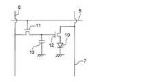
図2は、表示部Aの模式図である。
表示部Aは基板上に、複数の走査線5及びデータ線6を含む配線部と、複数の画素3等とを有する。表示部Aの主要な部材の説明を以下に行う。
【0146】
図においては、画素3の発光した光が、白矢印方向(下方向)へ取り出される場合を示している。
【0147】
配線部の走査線5及び複数のデータ線6は、それぞれ導電材料からなり、走査線5とデータ線6は格子状に直交して、直交する位置で画素3に接続している(詳細は図示せず)。
【0148】
画素3は、走査線5から走査信号が印加されると、データ線6から画像データ信号を受け取り、受け取った画像データに応じて発光する。発光の色が赤領域の画素、緑領域の画素、青領域の画素を、適宜、同一基板上に並置することによって、フルカラー表示が可能となる。
【0149】
次に、画素の発光プロセスを説明する。
図3は、画素の模式図である。
【0150】
画素は、有機EL素子10、スイッチングトランジスタ11、駆動トランジスタ12、コンデンサ13等を備えている。複数の画素に有機EL素子10として、赤色、緑色、青色発光の有機EL素子を用い、これらを同一基板上に並置することでフルカラー表示を行うことができる。
【0151】
図3において、制御部Bからデータ線6を介してスイッチングトランジスタ11のドレインに画像データ信号が印加される。そして、制御部Bから走査線5を介してスイッチングトランジスタ11のゲートに走査信号が印加されると、スイッチングトランジスタ11の駆動がオンし、ドレインに印加された画像データ信号がコンデンサ13と駆動トランジスタ12のゲートに伝達される。
【0152】
画像データ信号の伝達により、コンデンサ13が画像データ信号の電位に応じて充電されるとともに、駆動トランジスタ12の駆動がオンする。駆動トランジスタ12は、ドレインが電源ライン7に接続され、ソースが有機EL素子10の電極に接続されており、ゲートに印加された画像データ信号の電位に応じて電源ライン7から有機EL素子10に電流が供給される。
【0153】
制御部Bの順次走査により走査信号が次の走査線5に移ると、スイッチングトランジスタ11の駆動がオフする。しかし、スイッチングトランジスタ11の駆動がオフしてもコンデンサ13は充電された画像データ信号の電位を保持するので、駆動トランジスタ12の駆動はオン状態が保たれて、次の走査信号の印加が行われるまで有機EL素子10の発光が継続する。順次走査により次に走査信号が印加されたとき、走査信号に同期した次の画像データ信号の電位に応じて駆動トランジスタ12が駆動して有機EL素子10が発光する。
【0154】
すなわち、有機EL素子10の発光は、複数の画素それぞれの有機EL素子10に対して、アクティブ素子であるスイッチングトランジスタ11と駆動トランジスタ12を設けて、複数の画素3それぞれの有機EL素子10の発光を行っている。このような発光方法をアクティブマトリクス方式と呼んでいる。
【0155】
ここで、有機EL素子10の発光は、複数の階調電位を持つ多値の画像データ信号による複数の階調の発光でもよいし、2値の画像データ信号による所定の発光量のオン、オフでもよい。
【0156】
また、コンデンサ13の電位の保持は、次の走査信号の印加まで継続して保持してもよいし、次の走査信号が印加される直前に放電させてもよい。
本発明においては、上述したアクティブマトリクス方式に限らず、走査信号が走査されたときのみデータ信号に応じて有機EL素子を発光させるパッシブマトリクス方式の発光駆動でもよい。
【0157】
図4は、パッシブマトリクス方式による表示装置の模式図である。図4において、複数の走査線5と複数の画像データ線6が画素3を挟んで対向して格子状に設けられている。
順次走査により走査線5の走査信号が印加されたとき、印加された走査線5に接続している画素3が画像データ信号に応じて発光する。パッシブマトリクス方式では画素3にアクティブ素子が無く、製造コストの低減が計れる。
【0158】
【実施例】
以下、実施例を挙げて本発明を詳細に説明するが、本発明の態様はこれに限定されない。
【0159】
実施例1
〈有機EL素子の作製〉
有機EL素子を以下のように作製した。陽極として100mm×100mm×1.1mmのガラス基板上にITO(インジウムチンオキシド)を100nm成膜した基板(NHテクノグラス社製NA−45)にパターニングを行った後、このITO透明電極を設けた透明支持基板をイソプロピルアルコールで超音波洗浄し、乾燥窒素ガスで乾燥し、UVオゾン洗浄を5分間行なった。この透明支持基板を市販の真空蒸着装置の基板ホルダーに固定し、一方、モリブデン製抵抗加熱ボートにα−NPDを200mg入れ、別のモリブデン製抵抗加熱ボートにCBPを200mg入れ、別のモリブデン製抵抗加熱ボートにバソキュプロイン(BCP)を200mg入れ、別のモリブデン製抵抗加熱ボートに燐光性化合物Ir(ppy)3を100mg入れ、更に別のモリブデン製抵抗加熱ボートにAlq3を200mg入れ、真空蒸着装置に取付けた。
【0160】
次いで、真空槽を4×10⁻⁴Paまで減圧した後、α−NPDの入った前記加熱ボートに通電して加熱し、蒸着速度0.1nm/secで透明支持基板に蒸着し、膜厚25nmの正孔輸送層を設けた。更に、CBPと燐光性化合物Ir(ppy)3の入った前記加熱ボートに通電して加熱し、それぞれ蒸着速度0.2nm/sec、0.012nm/secで前記正孔輸送層上に共蒸着して膜厚35nmの発光層を設けた。尚、蒸着時の基板温度は室温であった。更に、BCPの入った前記加熱ボートに通電して加熱し、蒸着速度0.1nm/secで前記発光層の上に蒸着して膜厚10nmの正孔阻止の役割も兼ねた電子輸送層を設けた。その上に、更に、Alq3の入った前記加熱ボートに通電して加熱し、蒸着速度0.1nm/secで前記電子輸送層の上に蒸着して更に膜厚40nmの電子注入層を設けた。尚、蒸着時の基板温度は室温であった。
【0161】
引き続きフッ化リチウム0.5nm及びアルミニウム110nmを蒸着して陰極を形成し、有機EL素子OLED1−1を作製した。表1に示すその他の有機EL素子も、発光層に用いた化合物CBPを表1に示す化合物に置き換えた以外は全く同じ方法で有機EL素子OLED1−2〜1−18を作製した。上記で使用した化合物の構造を以下に示す。
【0162】
【化25】
【化26】
〈有機EL素子の評価〉
以上のようにして得られた有機EL素子の評価を行い、結果を表1に示す。
【0165】
(発光輝度、発光効率)
有機EL素子OLED1−1では、初期駆動電圧3Vで電流が流れ始め、発光層のドーパントである燐光性化合物からの緑色の発光を示した。有機EL素子OLED1−1の温度23℃、乾燥窒素ガス雰囲気下で10Vの直流電圧を印加した時の発光輝度(cd/m2)、発光効率(lm/W)を測定した。各有機EL素子の発光輝度、発光効率はいずれも有機EL素子OLED1−1についてそれぞれを100とした時の相対値で表した。尚、発光輝度については、CS−1000(ミノルタ製)を用いて測定した。
【0166】
(耐久性)
2.5mA/cm2の一定電流で駆動したときに初期輝度が元の半分に低下するのに要した時間である半減寿命時間を指標として表した。半減寿命時間についても有機EL素子OLED1−1を100とした時の相対値で表した。
【0167】
【表1】
表1から明らかなように、本発明に係る化合物をホスト化合物として用いた有機EL素子は、CBPに比べて発光輝度・発光効率・耐久性に優れ、さらに比較化合物1および2と比較した場合においても、発光輝度や発光効率で同等以上、耐久性においてはこれらを凌ぐ性能を示した。本発明の化合物をホストに用いた有機EL素子は、発光輝度、発光効率が改善され、耐久性が良いことから、有機EL素子として非常に有用であることがわかった。
【0169】
実施例2
実施例1の有機EL素子OLED1−1について、燐光性化合物Ir(ppy)3をFIr(pic)に置き換えた以外は全く同じ方法で、青色発光有機EL素子OLED2−1を作製した。次いで同様にして、発光層に用いたCBPを表2に示した化合物にかえて有機EL素子OLED2−2〜2−9を作製し、実施例1と同様の方法で発光輝度、発光効率を測定して得られた結果を、素子番号および発光層に使用した化合物とともに、表2に示した。
【0170】
【化27】
【表2】
表2から明らかなように、本発明の化合物を用いた有機EL素子は、同様に発光輝度および発光効率が顕著に改善されているのが分かる。
【0173】
実施例3
実施例1の有機EL素子OLED1−1と全く同じ有機EL素子OLED3−1を作製し、更に、電子輸送層に用いた化合物BCPを表3に示す化合物に置き換えた以外は、実施例1と全く同じ方法で緑色発光有機EL素子OLED3−2〜3−9を作製した。実施例1と同様の方法で発光輝度、発光効率および耐久性を測定して得られた結果を、素子番号および電子輸送層に使用した化合物とともに、表3に示す。
【0174】
【表3】
表3から明らかなように、本発明の化合物を電子輸送層に用いた有機EL素子は、発光輝度、発光効率、耐久性が改善されているのが分かる。とくに耐久性において、その改善の効果は顕著である。
【0176】
実施例4
前記実施例で作製したそれぞれ緑色および青色発光有機EL素子、および緑色発光有機EL素子の燐光性化合物をBtp2Ir(acac)に置き換えた以外は同様にして作製した赤色発光有機EL素子を同一基板上に並置し、図1、2に示すアクティブマトリクス方式フルカラー表示装置を作製した。
【0177】
【化28】
図2には作製したフルカラー表示装置の表示部Aの模式図のみを示した。即ち同一基板上に、複数の走査線5及びデータ線6を含む配線部と、並置した複数の画素3(発光の色が赤領域の画素、緑領域の画素、青領域の画素等)とを有し、配線部の走査線5及び複数のデータ線6はそれぞれ導電材料からなり、走査線5とデータ線6は格子状に直交して、直交する位置で画素3に接続している(詳細は図示せず)。前記複数画素3は、それぞれの発光色に対応した有機EL素子、アクティブ素子であるスイッチングトランジスタと駆動トランジスタそれぞれが設けられたアクティブマトリクス方式で駆動されており、走査線5から走査信号が印加されると、データ線6から画像データ信号を受け取り、受け取った画像データに応じて発光する。この様に各赤、緑、青の画素を適宜、並置することによって、フルカラー表示が可能となる。
【0179】
該フルカラー表示装置を駆動することにより、輝度の高く耐久性の良好な、鮮明なフルカラー動画表示が得られた。
【0180】
【発明の効果】
本発明により、高い発光輝度を示し、量子効率に優れ、かつ、半減寿命の長い有機EL素子及び表示装置を提供することができる。特に、青色発光において、発光輝度、発光効率及び耐久性の両立を達成した有機EL素子、及びそれを用いた発光輝度の高い、耐久性の良好な表示装置を提供することができる。
【図面の簡単な説明】
【図1】有機EL素子から構成される表示装置の一例を示した模式図である。
【図2】表示部の模式図である。
【図3】画素の模式図である。
【図4】パッシブマトリクス方式フルカラー表示装置の模式図である。
【符号の説明】
1 ディスプレイ
3 画素
5 走査線
6 データ線
7 電源ライン
10 有機EL素子
11 スイッチングトランジスタ
12 駆動トランジスタ
13 コンデンサ
A 表示部
B 制御部[0001]
TECHNICAL FIELD OF THE INVENTION
The present invention relates to an organic electroluminescence element (organic EL element) and a display device, and more particularly, to an organic electroluminescence element excellent in light emission luminance, light emission efficiency and durability, and a display device having the same in its configuration.
[0002]
[Prior art]
2. Description of the Related Art Conventionally, there is an electroluminescence display (ELD) as a light-emitting electronic display device. ELD includes an inorganic electroluminescence element and an organic electroluminescence element (also referred to as an organic EL element). Inorganic electroluminescent devices have been used as flat light sources, but require a high AC voltage to drive the light emitting devices.
[0003]
On the other hand, an organic electroluminescence element has a configuration in which a light-emitting layer containing a compound that emits light is sandwiched between a cathode and an anode, and electrons and holes are injected into the light-emitting layer and recombination causes exciton (exciton). ), And emits light by utilizing light emission (fluorescence / phosphorescence) when the exciton is deactivated. The device can emit light at a voltage of about several volts to several tens of volts. Since it is a light emitting type, it has a wide viewing angle and high visibility, and because it is a thin-film type solid-state element, it is attracting attention from the viewpoint of space saving and portability.
[0004]
As for the development of organic EL devices for practical use in the future, organic EL devices that emit light with high efficiency and low power consumption are desired. For example, stilbene derivatives, distyrylarylene derivatives or tristyrylarylene derivatives are desired. (See, for example, Patent Literature 1), an 8-hydroxyquinoline aluminum complex is used as a host compound, and a small amount of fluorescent light is added thereto. (For example, see Patent Document 2) and an element having an organic light-emitting layer in which an 8-hydroxyquinoline aluminum complex is used as a host compound and a quinacridone-based dye is doped therein (for example, see Patent Document 2). 3) is known.
[0005]
In the technique disclosed in the above-mentioned document, when light emission from an excited singlet is used, the generation ratio of a singlet exciton and a triplet exciton is 1: 3, so that the generation probability of a luminescent excited species is 25%. And the light extraction efficiency is about 20%, the external extraction quantum efficiency (ηext ) Is 5%.
[0006]
However, since Princeton University reported an organic EL device using phosphorescence from excited triplets (for example, see Non-Patent Document 1), research on materials that exhibit phosphorescence at room temperature has been active. (For example, see Non-Patent Document 2 and Patent Document 4.)
[0007]
When the excited triplet is used, the upper limit of the internal quantum efficiency becomes 100%. Therefore, the luminous efficiency is quadrupled in principle as compared with the case of the excited singlet, and the performance almost equal to that of the cold cathode tube is obtained. It is also applicable to and is attracting attention.
[0008]
For example, many compounds have been studied for synthesis centering on heavy metal complexes such as iridium complexes (for example, see Non-Patent Document 3).
[0009]
Also, studies using tris (2-phenylpyridine) iridium as a dopant have been made (for example, see Non-Patent Document 2).
[0010]
In addition, L as a dopant2 Ir (acac) [where L represents a ligand], for example, (ppy)2 Ir (acac) (for example, see Non-Patent Document 4) and tris (2- (p-tolyl) pyridine) iridium (Ir (ptpy)3 ), Tris (benzo [h] quinoline) iridium (Ir (bzq)3 ), Ir (bzq)2 ClP (Bu)3 (For example, see Non-Patent Document 5).
[0011]
Further, in order to obtain high luminous efficiency, a compound having a hole transporting property is used as a host of a phosphorescent compound (for example, see Non-Patent Document 6).
[0012]
Further, various electron-transporting materials are used as a host of a phosphorescent compound by doping them with a novel iridium complex (for example, see Non-Patent Document 4). Further, high luminous efficiency is obtained by introducing a hole blocking layer (for example, see Non-Patent Document 5).
[0013]
However, although the external extraction efficiency of about 20%, which is the theoretical limit, has been achieved for green light emission, other light emission colors have not yet been obtained with sufficient efficiency and need to be improved. In an organic EL device for practical use, further development of an organic EL device which emits light with high efficiency and low power consumption is desired.
[0014]
As described above, many compounds have been proposed to solve such problems. As one of such compounds, carbazole derivatives have been studied. For example,
[0015]
[Patent Document 1]
Japanese Patent No. 3093796
[0016]
[Patent Document 2]
JP-A-63-264692
[0017]
[Patent Document 3]
JP-A-3-255190
[0018]
[Patent Document 4]
U.S. Pat. No. 6,097,147
[0019]
[Patent Document 5]
JP-A-8-60144
[0020]
[Patent Document 6]
JP-A-5-194943
[0021]
[Patent Document 7]
JP 2001-257076 A
[0022]
[Patent Document 8]
JP 2002-100476 A
[0023]
[Non-patent document 1]
M. A. Baldo et al. , Nature, 395 volumes,
151-154 pages (1998)
[0024]
[Non-patent document 2]
M. A. Baldo et al. , Nature, Vol. 403, No. 17, pp. 750-753 (2000)
[0025]
[Non-Patent Document 3]
S. See Lamansky et al. , J. et al. Am. Chem. Soc. 123, 4304 pages (2001)
[0026]
[Non-patent document 4]
M. E. FIG. Thompson et al. , The 10th International Works on Inorganic and Organic Electroluminescence (EL'00, Hamamatsu)
[0027]
[Non-Patent Document 5]
Moon-Jae Youn. Og, Tetsuo Tsutsui et al. , The 10th International Works on Inorganic and Organic Electroluminescence (EL'00, Hamamatsu)
[0028]
[Non-Patent Document 6]
Ikai et al. , The 10th International Works on Inorganic and Organic Electroluminescence (EL'00, Hamamatsu)
[0029]
[Problems to be solved by the invention]
An object of the present invention is to provide an organic electroluminescence element (hereinafter, also abbreviated as an organic EL element) and a display device that exhibit high emission luminance, have excellent quantum efficiency, and have a long half-life. In particular, in the case of blue light emission, it is intended to achieve both the improvement of the light emission luminance, the luminous efficiency and the durability of the device. The present invention provides an organic electroluminescent device having achieved the above, and a display device having high light emission luminance and excellent durability using the organic electroluminescent device.
[0030]
[Means for Solving the Problems]
The above object of the present invention is achieved by the following means.
[0031]
1. In an organic electroluminescence device having at least one light-emitting layer and emitting light from the light-emitting layer including phosphorescence, at least one carbazole derivative represented by the general formula 1 is contained in any one of the layers constituting the device. An organic electroluminescent device, comprising:
[0032]
2. 2. The organic electroluminescence device according to the above 1, wherein the compound of the general formula 1 is contained in a light emitting layer.
[0033]
3. 3. The organic electroluminescent device according to the above 1 or 2, wherein n in the general formula 1 is 3, and the compound represented by the general formula 1 does not have a rotation axis three times as a whole molecule. .
[0034]
4. In the general formula 1, the aromatic ring residue skeleton portion of A is benzene, naphthalene, anthracene, pyrene, pyridine, pyridazine, pyrimidine, pyrazine, 1,2,4-triazine, pyrrole, furan, thiophene, or any of these. 4. The organic electroluminescent device according to any one of the above items 1 to 3, wherein the organic electroluminescent device is any one selected from an aromatic condensed ring condensed with a compound.
[0035]
5. 5. In the general formula 1, at least one of the n substituents Z has a structure different from the other Zs. 5. The organic electroluminescence according to any one of the above 1 to 4, wherein element.
[0036]
6. In the above general formula 1, the aromatic ring residue skeleton part of A is selected from benzene, pyridine, and 1,3,5-triazine. Organic electroluminescent element.
[0037]
7. In the general formula 2, L is a bond, arylene, heteroarylene, vinylene, -Si (R)2 -The organic electroluminescent device according to any one of the above items 1 to 6, wherein the organic electroluminescent device is selected from any one of-(R is a monovalent organic group).
[0038]
8. 8. The organic electroluminescent device according to the above 7, wherein L in the general formula 2 represents a bond.
[0039]
9. A display device comprising the organic electroluminescent element according to any one of the above items 1 to 8 in its configuration.
[0040]
Hereinafter, the compound of the present invention will be described in detail.
A in the general formula 1 represents an aromatic ring residue. Examples of the aromatic ring serving as the skeleton portion of the aromatic ring residue include benzene, pyridine, pyridazine, pyrimidine, pyrazine, 1,3,5-triazine, 1,2,4-triazine, pyrrole, imidazole, furan, and thiophene But further may be an aromatic condensed ring formed by an arbitrary combination of these rings, and examples of such an aromatic condensed ring include naphthalene, anthracene, dithienobenzene, carbazole, and quinoline. . Further, it may be a condensed aromatic ring other than those mentioned above, such as fluorene, azulene and phenothiazine.
[0041]
These aromatic rings may have a substituent, and examples of the substituent include an alkyl group (for example, a methyl group, an ethyl group, a propyl group, an isopropyl group, a (t) butyl group, a pentyl group, a hexyl group). Octyl group, dodecyl group, tridecyl group, tetradecyl group, pentadecyl group, etc.), cycloalkyl group (eg, cyclopentyl group, cyclohexyl group, etc.), alkenyl group (eg, vinyl group, allyl group, etc.), alkynyl group (eg, A propargyl group, an aryl group (eg, phenyl group, naphthyl group, etc.), a heterocyclic group (eg, pyridyl group, thiazolyl group, oxazolyl group, imidazolyl group, furyl group, pyrrolyl group, pyrazinyl group, pyrimidinyl group, pyridazinyl group) , Selenazolyl, sulfolanyl, piperidinyl, pyrazolyl, tetrazolyl ), Halogen atoms (eg, chlorine atom, bromine atom, iodine atom, fluorine atom, etc.), alkoxy groups (eg, methoxy group, ethoxy group, propyloxy group, pentyloxy group, hexyloxy group, octyloxy group, dodecyloxy) Group), cycloalkoxyl group (eg, cyclopentyloxy group, cyclohexyloxy group, etc.), aryloxy group (eg, phenoxy group, naphthyloxy group, etc.), alkylthio group (eg, methylthio group, ethylthio group, propylthio group, pentylthio group) Group, hexylthio group, octylthio group, dodecylthio group, etc.), cycloalkylthio group (eg, cyclopentylthio group, cyclohexylthio group, etc.), arylthio group (eg, phenylthio group, naphthylthio group, etc.), alkoxycarbonyl group (eg, Tyloxycarbonyl group, ethyloxycarbonyl group, butyloxycarbonyl group, octyloxycarbonyl group, dodecyloxycarbonyl group, etc., aryloxycarbonyl group (eg, phenyloxycarbonyl group, naphthyloxycarbonyl group, etc.), sulfamoyl group (eg, , Aminosulfonyl group, methylaminosulfonyl group, dimethylaminosulfonyl group, butylaminosulfonyl group, hexylaminosulfonyl group, cyclohexylaminosulfonyl group, octylaminosulfonyl group, dodecylaminosulfonyl group, phenylaminosulfonyl group, naphthylaminosulfonyl group, 2-pyridylaminosulfonyl group, etc.), ureido group (for example, methylureido group, ethylureido group, pentylureido group, cyclohexylureido) Group, octylureido group, dodecylureido group, phenylureido group, naphthylureido group, 2-pyridylaminoureido group, etc.), acyl group (for example, acetyl group, ethylcarbonyl group, propylcarbonyl group, pentylcarbonyl group, cyclohexylcarbonyl group, Octylcarbonyl group, 2-ethylhexylcarbonyl group, dodecylcarbonyl group, phenylcarbonyl group, naphthylcarbonyl group, pyridylcarbonyl group, etc., acyloxy group (for example, acetyloxy group, ethylcarbonyloxy group, butylcarbonyloxy group, octylcarbonyloxy) Group, dodecylcarbonyloxy group, phenylcarbonyloxy group, etc.), amide group (for example, methylcarbonylamino group, ethylcarbonylamino group, dimethylcarbonylamino group, Propylcarbonylamino group, pentylcarbonylamino group, cyclohexylcarbonylamino group, 2-ethylhexylcarbonylamino group, octylcarbonylamino group, dodecylcarbonylamino group, phenylcarbonylamino group, naphthylcarbonylamino group, etc., carbamoyl group (for example, Aminocarbonyl group, methylaminocarbonyl group, dimethylaminocarbonyl group, propylaminocarbonyl group, pentylaminocarbonyl group, cyclohexylaminocarbonyl group, octylaminocarbonyl group, 2-ethylhexylaminocarbonyl group, dodecylaminocarbonyl group, phenylaminocarbonyl group , Naphthylaminocarbonyl group, 2-pyridylaminocarbonyl group, etc.), sulfinyl group (for example, methylsulfinyl group, Rusulfinyl group, butylsulfinyl group, cyclohexylsulfinyl group, 2-ethylhexylsulfinyl group, dodecylsulfinyl group, phenylsulfinyl group, naphthylsulfinyl group, 2-pyridylsulfinyl group, etc., alkylsulfonyl group or arylsulfonyl group (for example, methylsulfonyl) Group, ethylsulfonyl group, butylsulfonyl group, cyclohexylsulfonyl group, 2-ethylhexylsulfonyl group, dodecylsulfonyl group, phenylsulfonyl group, naphthylsulfonyl group, 2-pyridylsulfonyl group, etc.), amino group (for example, amino group, ethylamino Group, dimethylamino group, butylamino group, cyclopentylamino group, 2-ethylhexylamino group, dodecylamino group, anilino group, naphthylamino group, 2-pyri A nitro group, a cyano group, a hydroxyl group, a halogen atom and the like. These groups may be further substituted by the above substituents, or they may be condensed with each other to form a ring.
[0042]
Z in the general formula 1 is a structure represented by the general formula 2, and n represents an integer of 3 to 6. A preferred value for n is 3.
[0043]
In the general formula 2, L represents a bond (here, a bond means a bond directly connecting the substituents to be linked) or a divalent linking group, and the divalent linking group is alkylene; In addition to hydrocarbon groups such as alkenylene, alkynylene, and arylene, those containing a hetero atom may be used. For example, it may be a divalent linking group derived from a heteroaromatic compound such as a thiophene-2,5-diyl group or a pyrazine-2,3-diyl group, or may be a chalcogen atom such as oxygen or sulfur. There may be. Further, a group such as an alkylimino group, a dialkylsilanediyl group, or a diarylgermandiyl group, which connects heteroatoms to link A of the general formula 1 and Cz of the general formula 2 may be used. These linking groups may be substituted, and examples of the substituent include the same examples as described for A in Formula 1. Preferred as L in the general formula 2 is a bond, an arylene, a heteroarylene, an alkenylene, a disubstituted silicon atom, or a linking group formed by any combination thereof.
[0044]
Cz in the general formula 2 represents a substituted or unsubstituted carbazole residue. Examples of the substituent include the same examples as described for A in the general formula 1. Preferably an alkyl group, an alkoxy group, a fluoroalkyl group, an alkylthio group, an aryl group, a heterocyclic group, a halogen atom, a cyano group, particularly preferably an alkyl group, a fluoroalkyl group, an aryl group, a heterocyclic group, a fluorine atom, It is a cyano group. The bonding position with L is not particularly limited, but it is preferable that the carbazole is bonded to L at the 2-, 3-, or 9-position (N-position).
[0045]
The compound according to the present invention has a structure in which 3 to 6 carbazole derivative residues are bonded to an aromatic ring residue directly or via a linking group. When the number of bonded carbazole derivative residues is n, the molecule is characterized by having no rotation axis n times. For example, in the case of the compound represented by the following structural formula 1, three carbazole residues are bonded to a benzene ring as an aromatic ring skeleton, and this molecule is three times perpendicular to the plane formed by the benzene ring skeleton. Has a rotating axis. Therefore, a molecule having n carbazole derivative residues has a rotation axis of n times, and the compound of Structural Formula 1 is out of the scope of the present invention. In contrast, the compound of structural formula 2 has a structure in which three identical carbazole residues are bonded to an aromatic ring residue, but the carbazole residue is bonded to the pyridazine ring. Although a two-fold rotation axis is left in the direction connecting the carbon atom and the 4-position carbon atom, the three-fold rotation axis has disappeared, and the compound belongs to the category of the present invention. Furthermore, considering a molecule in which the same three carbazole residues are bonded to a pyrazine ring as in
[0046]
Embedded image
Embedded image
Embedded image
In the present invention, compounds having n different structures represented by Z in the general formula 1 are preferably used. For example, in the structural formulas 1 to 3, the skeleton structure A of the aromatic ring residue in the general formula 1 is different, and the partial structure represented by Z is the same carbazolyl group. If some of them are different compounds, they belong to the category of the present invention in which a compound having n partial structures Z does not have an n-fold rotation axis. When the partial structure represented by Z in the general formula 1 is different, the structure of the carbazole derivative residue represented by Cz in the general formula 2 may be different as in the compound shown in the
[0050]
Embedded image
The compound according to the present invention can be used for any of a hole transport layer, an electron transport layer, and a light-emitting layer of an organic electroluminescence (EL) device described below, but is preferably an electron transport layer or a light-emitting layer, and particularly preferably. Has excellent quantum efficiency and emission brightness when used as a material known as a “host compound” to engineers engaged in the art without transferring light to the phosphorescent compound in the light emitting layer and emitting light by itself. In particular, it is possible to manufacture an organic EL device exhibiting high performance particularly in durability. The reason why the compound according to the present invention can exhibit excellent properties with respect to known materials or the mechanism of operation is not unclear, but the molecular structural feature of having no symmetry is that it can be used during continuous operation or storage. At times, it is speculated that this is because an undesired phenomenon of preventing the normal operation of the light emitting mechanism due to crystallization of a part of the compound in the material thin film is prevented. In other words, the compound of Structural Formula 1 having three carbazole derivative residues and a three-fold rotation axis easily transitions from an amorphous state to a crystalline state during continuous operation or storage due to its symmetry. Since the compound of the present invention does not adopt a propeller-type highly symmetric conformation, it does not easily crystallize, and is therefore maintained as an amorphous material thin film for a long period of time. It is considered that this is suitable for manufacturing an EL element.
[0052]
Specific examples of the compound according to the present invention are shown below, but the embodiments of the present invention are not limited by these compound examples as long as the purpose of the present invention is not exceeded.
[0053]
Embedded image
Embedded image
Embedded image
Embedded image
Embedded image
Embedded image
Embedded image
Embedded image
Embedded image
Embedded image
Embedded image
Embedded image
Further, the molecular weight of the compound of the present invention is preferably from 600 to 2,000. When the molecular weight is from 600 to 2,000, Tg (glass transition temperature) is increased, thermal stability is improved, and the life of the device is improved. A more preferred molecular weight is from 800 to 2,000.
[0066]
The compounds according to the invention are described in Tetrahedron Lett. , 39 (1998), pp. 2367-2370, Japanese Patent No. 3161360, Angew. Chem. Int. Ed. , 37 (1998), pp. 2046-2067, Tetrahedron Lett. , 41 (2000), 481-484, Synth. Commun. , 11 (7) (1981), pp. 513-519, and Chem. Rev .. , 2002, 102, 1359-1469, and the like, and can be produced by a synthesis method known to those skilled in the art. The following shows typical synthetic routes for some of the exemplified compounds.
[0067]
Embedded image
Embedded image
Embedded image
<< Constituent Layer of Organic EL Element >>
The constituent layers of the organic EL device of the present invention will be described.
[0071]
In the present invention, preferred specific examples of the layer constitution of the organic EL element are shown below, but the present invention is not limited to these.
(I) anode / light-emitting layer / electron transport layer / cathode
(Ii) anode / hole transport layer / light-emitting layer / electron transport layer / cathode
(Iii) anode / hole transport layer / emission layer / hole blocking layer / electron transport layer / cathode
(Iv) anode / hole transport layer / emission layer / hole blocking layer / electron transport layer / cathode buffer layer / cathode
(V) anode / anode buffer layer / hole transport layer / emission layer / hole blocking layer / electron transport layer / cathode buffer layer / cathode
"anode"
As the anode in the organic EL element, a metal, an alloy, an electrically conductive compound, or a mixture thereof having a large work function (4 eV or more) as an electrode material is preferably used. Specific examples of such an electrode material include metals such as Au, CuI, indium tin oxide (ITO), and SnO.2 , ZnO and the like. In addition, IDIXO (In2 O3 A material capable of forming an amorphous transparent conductive film, such as —ZnO), may be used. The anode may be formed into a thin film by depositing or depositing these electrode substances by a method such as vapor deposition or sputtering, and may be formed into a pattern having a desired shape by a photolithography method. Degree), a pattern may be formed through a mask having a desired shape at the time of vapor deposition or sputtering of the electrode material. When light is extracted from the anode, the transmittance is desirably greater than 10%, and the sheet resistance of the anode is preferably several hundred Ω / □ or less. Further, the thickness depends on the material, but is usually selected in the range of 10 to 1000 nm, preferably 10 to 200 nm.
[0072]
"cathode"
On the other hand, as a cathode, a metal having a small work function (4 eV or less) (referred to as an electron injecting metal), an alloy, an electrically conductive compound, and a mixture thereof are used as an electrode material. Specific examples of such an electrode material include sodium, sodium-potassium alloy, magnesium, lithium, magnesium / copper mixture, magnesium / silver mixture, magnesium / aluminum mixture, magnesium / indium mixture, aluminum / aluminum oxide (Al2 O3 ) Mixtures, indium, lithium / aluminum mixtures, rare earth metals and the like. Among them, from the viewpoint of electron injecting property and durability against oxidation, etc., a mixture of an electron injecting metal and a second metal which is a stable metal having a large work function, such as a magnesium / silver mixture, magnesium / Aluminum mixture, magnesium / indium mixture, aluminum / aluminum oxide (Al2 O3 ) Mixtures, lithium / aluminum mixtures, aluminum and the like are preferred. The cathode can be manufactured by forming a thin film from these electrode substances by a method such as evaporation or sputtering. Further, the sheet resistance as the cathode is preferably several hundred Ω / □ or less, and the film thickness is usually selected in the range of 10 nm to 5 μm, preferably 50 nm to 200 nm. In order to transmit light, if one of the anode and the cathode of the organic EL element is transparent or translucent, the light emission luminance is advantageously improved.
[0073]
In addition, after preparing the above metal on the cathode in a thickness of 1 to 20 nm, a transparent or translucent cathode can be prepared by forming the conductive transparent material described in the description of the anode thereon. Thus, an element in which both the anode and the cathode have transparency can be manufactured.
[0074]
Next, an injection layer, a hole transport layer, an electron transport layer, and the like used as constituent layers of the organic EL device of the present invention will be described.
[0075]
<< Injection layer >>: electron injection layer, hole injection layer
The injection layer is provided as necessary, and has an electron injection layer and a hole injection layer, and exists between the anode and the light emitting layer or the hole transport layer, and between the cathode and the light emitting layer or the electron transport layer as described above. You may let it.
[0076]
The injection layer is a layer provided between an electrode and an organic layer for lowering the driving voltage and improving the light emission luminance. “The organic EL element and the forefront of its industrialization (published by NTT Corporation on November 30, 1998) )), Vol. 2, Chapter 2, “Electrode Materials” (pages 123 to 166), which includes a hole injection layer (anode buffer layer) and an electron injection layer (cathode buffer layer).
[0077]
The details of the anode buffer layer (hole injection layer) are described in JP-A-9-45479, JP-A-9-260062, and JP-A-8-288069, and specific examples thereof include copper phthalocyanine. Typical examples include a phthalocyanine buffer layer, an oxide buffer layer represented by vanadium oxide, an amorphous carbon buffer layer, and a polymer buffer layer using a conductive polymer such as polyaniline (emeraldine) or polythiophene.
[0078]
The details of the cathode buffer layer (electron injection layer) are also described in JP-A-6-325871, JP-A-9-17574, and JP-A-10-74586, and specifically, strontium and aluminum. A buffer layer such as a metal buffer layer, an alkali metal compound buffer layer such as lithium fluoride, an alkaline earth metal compound buffer layer such as magnesium fluoride, and an oxide buffer layer such as aluminum oxide. . The buffer layer (injection layer) is desirably a very thin film, and its thickness is preferably in the range of 0.1 nm to 5 μm, depending on the material.
[0079]
<< blocking layer >>: hole blocking layer, electron blocking layer
As described above, the blocking layer is provided as needed in addition to the basic constituent layers of the organic compound thin film. For example, it is described in JP-A-11-204258 and JP-A-11-204359, and on page 237 of "Organic EL Devices and Their Forefront of Industrialization (published by NTT Corporation on November 30, 1998)". There is a hole blocking (hole block) layer.
[0080]
The hole blocking layer is an electron transporting layer in a broad sense, and is made of a material having a function of transporting electrons and having an extremely small ability to transport holes. And the recombination probability of holes can be improved.
[0081]
On the other hand, an electron blocking layer is a hole transporting layer in a broad sense, and is made of a material that has a function of transporting holes and has a very small ability to transport electrons, and it blocks electrons while transporting holes. Thus, the recombination probability of electrons and holes can be improved.
[0082]
The hole transport layer is made of a material having a function of transporting holes. In a broad sense, a hole injection layer and an electron blocking layer are also included in the hole transport layer. The hole transport layer and the electron transport layer can be provided as a single layer or a plurality of layers.
[0083]
In the organic EL device of the present invention, the excited triplet energy of the host of the light-emitting layer, the hole transport layer adjacent to the light-emitting layer, and the material of the electron transport layer adjacent to the light-emitting layer are all the triplet energy of the phosphorescent dopant. It is preferably larger than. In particular, the wavelength of the 0-0 band in the phosphorescence spectrum of the host of the light emitting layer, the hole transport layer adjacent to the light emitting layer, and the electron transport layer adjacent to the light emitting layer is preferably 450 nm or less.
[0084]
<< Light-emitting layer >>
The light-emitting layer according to the present invention is an electrode or an electron-transport layer, a layer that emits light by recombination of electrons and holes injected from the hole-transport layer, and a light-emitting portion is in the light-emitting layer. May be the interface between the light emitting layer and the adjacent layer.
[0085]
The material used for the light-emitting layer (hereinafter, referred to as a light-emitting material) is preferably an organic compound or complex that emits fluorescence or phosphorescence, and is appropriately selected from known materials used for the light-emitting layer of the organic EL device. Can be used. Such a light emitting material is mainly an organic compound, and according to a desired color tone, for example, Macromol. Synth. And the like, vol. 125, pp. 17-25.
[0086]
The light emitting material may have a hole transport function and an electron transport function in addition to the light emitting performance, and most of the hole transport material and the electron transport material can be used as the light emitting material. The light-emitting material may be a polymer material such as p-polyphenylenevinylene or polyfluorene. Further, a polymer material in which the light-emitting material is introduced into a polymer chain or a polymer material in which the light-emitting material is a polymer main chain is used. May be.
[0087]
This light emitting layer can be formed by forming the above compound into a thin film by a known thinning method such as a vacuum evaporation method, a spin coating method, a casting method, and an LB method. The thickness of the light emitting layer is not particularly limited, but is usually selected in the range of 5 nm to 5 μm, preferably 5 nm to 200 nm. This light-emitting layer may have a single-layer structure composed of one or two or more of these light-emitting materials, or may have a laminated structure composed of a plurality of layers having the same composition or different compositions. A preferred embodiment of the organic EL device of the present invention is when the light-emitting layer is composed of two or more materials, one of which is the compound of the present invention.
[0088]
Further, as described in JP-A-57-51781, this light-emitting layer is prepared by dissolving the light-emitting material together with a binder such as a resin in a solvent to form a solution, and then spin-coating the solution. It can be formed as a thin film. The thickness of the light emitting layer formed in this manner is not particularly limited and can be appropriately selected depending on the situation, but is usually in the range of 5 nm to 5 μm, and preferably in the range of 5 to 200 nm.
[0089]
《Host compound》
The “host compound (also simply referred to as a host)” means a compound having the largest mixing ratio (mass) in a light-emitting layer composed of two or more compounds, and a “dopant” for other compounds. Compound (also simply referred to as dopant). " For example, the light-emitting layer is composed of two kinds of compound A and compound B, and if the mixing ratio is A: B = 10: 90, compound A is a dopant compound and compound B is a host compound. Further, the light emitting layer is composed of three kinds of compound A, compound B and compound C, and if the mixing ratio is A: B: C = 5: 10: 85, compound A and compound B are dopant compounds, Compound C is the host compound.
[0090]
The host compound of the light emitting layer is preferably an organic compound or a complex. In the present invention, the host compound preferably has an excited triplet energy larger than that of the phosphorescent dopant. Further, the wavelength of the 0-0 band in the phosphorescence spectrum of the host compound is preferably 450 nm or less. This allows visible light, especially BGR light emission.
[0091]
That is, by making the excited triplet energy of the host compound larger than the excited triplet energy of the phosphorescent dopant, an energy transfer type dopant emission from the host compound to the dopant is possible. Further, a compound in which the wavelength of the 0-0 band in the phosphorescence spectrum of the host compound is 450 nm or less has a very wide energy gap (ionization potential-electron affinity, HOMO-LUMO), and thus works advantageously for a carrier trap type.
[0092]
As such a host compound, any one of known compounds used in an organic EL device can be selected and used, and most of the hole transporting material and the electron transporting material described later are composed of a light emitting layer host compound. Can also be used as
[0093]
A polymer material such as polyvinyl carbazole or polyfluorene may be used, and a polymer material in which the host compound is introduced into a polymer chain or in which the host compound is a polymer main chain may be used.
[0094]
As the host compound, a compound which has a hole-transporting ability and an electron-transporting ability, prevents a long wavelength emission, and has a high Tg (glass transition temperature) is preferable.
[0095]
《Dopant》
Next, the dopant will be described.
[0096]
In principle, there are two types. One is that the recombination of carriers occurs on the host where the carriers are transported, the excited state of the host compound is generated, and light is emitted from the dopant by transferring this energy to the dopant. The other is the energy transfer type, and the other is the carrier trap type, in which the dopant becomes a carrier trap, the carriers recombine on the dopant compound, and light emission from the dopant is obtained, but in any case, the excitation of the dopant compound The condition is that the energy of the state is lower than the energy of the excited state of the host compound.
[0097]
The “phosphorescent dopant” and the “phosphorescent compound” in the present invention are compounds in which light emission from excited triplet is observed, and have a phosphorescence quantum yield of 0.001 or more at 25 ° C. The phosphorescence quantum yield is preferably at least 0.01, more preferably at least 0.1.
[0098]
The phosphorescence quantum yield can be measured by the method described in Spectroscopy II, 4th Edition, Experimental Chemistry Course, Spectroscopy II, p. 398 (1992 edition, Maruzen). Although the phosphorescence quantum yield in a solution can be measured using various solvents, the phosphorescent dopant used in the present invention only needs to achieve the above-mentioned phosphorescence quantum yield in any of the solvents.
[0099]
The phosphorescent dopant used in the present invention is preferably a complex compound containing a metal belonging to Group 8 of the periodic table of the elements, and more preferably an iridium compound, an osmium compound, or a platinum compound (platinum complex compound). , Rare earth complexes, among which the most preferred are iridium compounds.
[0100]
Hereinafter, specific examples of the phosphorescent compound used in the present invention are shown, but the invention is not limited thereto. These compounds are described, for example, in Inorg. Chem. 40, 1704-1711.
[0101]
Embedded image
Embedded image
Embedded image
The maximum phosphorescent emission wavelength of the phosphorescent compound to be used is not particularly limited, and in principle, the emission wavelength obtained by selecting a central metal, a ligand, a substituent of the ligand, and the like can be used. Can be changed. Further, plural kinds of host compounds and phosphorescent dopants may be used. By using a plurality of types of host compounds, it is possible to adjust the transfer of electric charges, and to increase the efficiency of the organic EL device. Further, by using a plurality of kinds of phosphorescent dopants, different luminescence can be mixed, whereby an arbitrary luminescent color can be obtained. By adjusting the type and amount of the phosphorescent dopant, white light emission is possible, and application to illumination and backlight is also possible.
[0105]
In another embodiment, in addition to the host compound and the phosphorescent compound, at least one fluorescent compound having a fluorescence maximum wavelength may be contained in a region longer than the maximum wavelength of light emission from the phosphorescent compound. . In this case, by the energy transfer from the host compound and the phosphorescent compound to the fluorescent compound, the electroluminescence as the organic EL device is obtained by the light emission from the fluorescent compound. Preferred as the fluorescent compound is a compound having a high fluorescence quantum yield in a solution state. Here, the fluorescence quantum yield is preferably 10% or more, particularly preferably 30% or more. Specific fluorescent compounds include coumarin dyes, pyran dyes, cyanine dyes, croconium dyes, squarium dyes, oxobenzanthracene dyes, fluorescein dyes, rhodamine dyes, pyrylium dyes, perylene dyes, Stilbene dyes, polythiophene dyes and the like can be mentioned. The fluorescence quantum yield can be measured by the method described in Spectroscopy II, p. 362 (1992 edition, Maruzen) of the 4th edition of
[0106]
In this specification, the emission color is measured by a spectral radiance meter CS-1000 (manufactured by Minolta) in FIG. It is determined by the color when the measured result is applied to the CIE chromaticity coordinates.
[0107]
This light emitting layer can be formed by thinning a phosphorescent dopant and a host compound by a known method such as a vacuum evaporation method, a spin coating method, a casting method, a printing method including an inkjet method, an LB method, or the like. it can. The thickness of the light emitting layer is not particularly limited, but is usually about 5 nm to 5 μm, preferably 5 to 200 nm.
[0108]
《Hole transport layer》
The hole transport layer is made of a material having a function of transporting holes. In a broad sense, a hole injection layer and an electron blocking layer are also included in the hole transport layer. The hole transport layer can be provided as a single layer or a plurality of layers.
[0109]
The hole transporting material is not particularly limited, and is conventionally used in a photoconductive material as a material commonly used as a hole charge injecting and transporting material, and used in a hole injecting layer and a hole transporting layer of an organic EL device. Any one of known ones can be selected and used.
[0110]
The hole transport material has any of hole injection or transport and electron barrier properties, and may be an organic substance or an inorganic substance. For example, triazole derivatives, oxadiazole derivatives, imidazole derivatives, polyarylalkane derivatives, pyrazoline derivatives and pyrazolone derivatives, phenylenediamine derivatives, arylamine derivatives, amino-substituted chalcone derivatives, oxazole derivatives, styryl anthracene derivatives, fluorenone derivatives, hydrazone derivatives, stilbenes Derivatives, silazane derivatives, aniline-based copolymers, conductive polymer oligomers, especially thiophene oligomers, and the like can be given.
[0111]
As the hole transporting material, those described above can be used, but it is preferable to use a porphyrin compound, an aromatic tertiary amine compound and a styrylamine compound, particularly an aromatic tertiary amine compound.
[0112]
Representative examples of the aromatic tertiary amine compound and styrylamine compound include N, N, N ', N'-tetraphenyl-4,4'-diaminophenyl; N, N'-diphenyl-N, N'- Bis (3-methylphenyl)-[1,1'-biphenyl] -4,4'-diamine (TPD); 2,2-bis (4-di-p-tolylaminophenyl) propane; 1,1-bis (4-di-p-tolylaminophenyl) cyclohexane; N, N, N ', N'-tetra-p-tolyl-4,4'-diaminobiphenyl; 1,1-bis (4-di-p-tolyl Aminophenyl) -4-phenylcyclohexane; bis (4-dimethylamino-2-methylphenyl) phenylmethane; bis (4-di-p-tolylaminophenyl) phenylmethane; N, N'-diphenyl-N, N ' − (4-methoxyphenyl) -4,4'-diaminobiphenyl; N, N, N ', N'-tetraphenyl-4,4'-diaminodiphenyl ether; 4,4'-bis (diphenylamino) quadriphenyl; N, N, N-tri (p-tolyl) amine; 4- (di-p-tolylamino) -4 '-[4- (di-p-tolylamino) styryl] stilbene; 4-N, N-diphenylamino- (2-diphenylvinyl) benzene; 3-methoxy-4'-N, N-diphenylaminostilbenzene; N-phenylcarbazole, and two of those described in U.S. Pat. No. 5,061,569. Having a condensed aromatic ring in the molecule thereof, for example, 4,4'-bis [N- (1-naphthyl) -N-phenylamino] biphenyl (NPD), JP-A-4-3086 No. 8,4,4 ', 4 "-tris [N- (3-methylphenyl) -N-phenylamino] triphenylamine in which three triphenylamine units are connected in a starburst form. MTDATA) and the like.
[0113]
Further, a polymer material in which these materials are introduced into a polymer chain, or a polymer material in which these materials are used as a polymer main chain can be used. Further, inorganic compounds such as p-type Si and p-type SiC can also be used as the hole injection material and the hole transport material.
[0114]
In the present invention, it is preferable that the excited triplet energy of the hole transport material of the hole transport layer adjacent to the light emitting layer is larger than the excited triplet energy of the phosphorescent dopant. Further, it is preferable that the wavelength of the 0-0 band in the phosphorescence spectrum of the hole transporting material of the hole transporting layer adjacent to the light emitting layer is 450 nm or less. That is, the hole transporting material is preferably a compound having hole transporting ability, preventing deactivation of light emission from the phosphorescent dopant, and having a high Tg.
[0115]
The hole transport layer is formed by thinning the hole transport material by a known method such as a vacuum deposition method, a spin coating method, a casting method, a printing method including an inkjet method, an LB method, or the like. Can be. The thickness of the hole transport layer is not particularly limited, but is usually about 5 nm to 5 μm, preferably 5 to 200 nm. The hole transport layer may have a single-layer structure made of one or more of the above materials.
[0116]
《Electron transport layer》
The electron transport layer is made of a material having a function of transporting electrons. In a broad sense, the electron transport layer includes an electron injection layer and a hole blocking layer. The electron transport layer can be provided as a single layer or a plurality of layers.
[0117]
The electron transporting layer only needs to have a function of transmitting electrons injected from the cathode to the light emitting layer, and any material can be selected from conventionally known compounds.
[0118]
Conventionally, the following materials are used as an electron transporting material (also serving as a hole blocking material) used for a single layer of an electron transporting layer and an electron transporting layer adjacent to the light emitting layer on the cathode side with respect to the light emitting layer. Are known.
[0119]
Examples of materials used for the electron transporting layer (hereinafter, referred to as electron transporting materials) include nitro-substituted fluorene derivatives, diphenylquinone derivatives, thiopyran dioxide derivatives, carbodiimides, fluorenylidenemethane derivatives, anthraquinodimethanes, and anthrone derivatives. And oxadiazole derivatives. Further, in the oxadiazole derivative, a thiadiazole derivative in which an oxygen atom of the oxadiazole ring is substituted with a sulfur atom, and a quinoxaline derivative having a quinoxaline ring known as an electron withdrawing group can also be used as the electron transport material.
[0120]
Further, a polymer material in which these materials are introduced into a polymer chain, or a polymer material in which these materials are used as a polymer main chain can be used.
[0121]
Further, a metal complex of an 8-quinolinol derivative, for example, tris (8-quinolinol) aluminum (Alq), tris (5,7-dichloro-8-quinolinol) aluminum, tris (5,7-dibromo-8-quinolinol) aluminum, Tris (2-methyl-8-quinolinol) aluminum, tris (5-methyl-8-quinolinol) aluminum, bis (8-quinolinol) zinc (Znq), and the like, and the central metals of these metal complexes are In, Mg, Cu , Ca, Sn, Ga or Pb can also be used as the electron transport material. In addition, metal-free or metal phthalocyanine, or those whose terminals are substituted with an alkyl group, a sulfonic acid group, or the like, can also be preferably used as the electron transport material. Further, the distyrylpyrazine derivative exemplified as the material of the light emitting layer can be used as the electron transporting material, and like the hole injection layer and the hole transport layer, inorganic materials such as n-type Si and n-type SiC can be used. Semiconductors can also be used as electron transport materials.
[0122]
Further, in the present invention, it is preferable that the excited triplet energy of the electron transporting material of the electron transporting layer adjacent to the light emitting layer is larger than the excited triplet energy of the phosphorescent dopant. Further, the wavelength of the 0-0 band in the phosphorescence spectrum of the electron transporting material of the electron transporting layer adjacent to the light emitting layer is preferably 450 nm or less.
[0123]
The electron transport layer can be formed by thinning the electron transport material by a known method such as a vacuum deposition method, a spin coating method, a casting method, a printing method including an inkjet method, an LB method, and the like. . The thickness of the electron transport layer is not particularly limited, but is usually about 5 nm to 5 μm, preferably 5 to 200 nm. The electron transport layer may have a single-layer structure made of one or more of the above materials.
[0124]
<< Substrate (also referred to as substrate, substrate, support, etc.) >>
The substrate of the organic EL device of the present invention is not particularly limited in the type of glass, plastic, and the like, and is not particularly limited as long as it is transparent. A light-transmitting resin film can be used. A particularly preferred substrate is a resin film that can provide flexibility to the organic EL element.
[0125]
Examples of the resin film include polyethylene terephthalate (PET), polyethylene naphthalate (PEN), polyether sulfone (PES), polyether imide, polyether ether ketone, polyphenylene sulfide, polyarylate, polyimide, polycarbonate (PC), and cellulose triacetate. (TAC), cellulose acetate propionate (CAP) and the like. An inorganic or organic film or a hybrid film of both may be formed on the surface of the resin film.
[0126]
The external extraction efficiency at room temperature of light emission of the organic electroluminescence device of the present invention is preferably 1% or more, more preferably 5% or more. Here, the external extraction quantum efficiency (%) = the number of photons emitted to the outside of the organic EL element / the number of electrons flowing to the organic EL element × 100.
[0127]
Further, a hue improvement filter such as a color filter may be used in combination, or a color conversion filter for converting the emission color of the organic EL element into multiple colors using a phosphor may be used in combination. When a color conversion filter is used, λmax of light emission of the organic EL element is preferably 480 nm or less.
[0128]
<< Method of manufacturing organic EL element >>
As an example of a method for manufacturing an organic EL device of the present invention, a method for manufacturing an organic EL device including an anode / a hole injection layer / a hole transport layer / a light emitting layer / an electron transport layer / an electron injection layer / a cathode will be described.
[0129]
First, a thin film made of a desired electrode material, for example, a material for an anode is formed on an appropriate substrate by a method such as vapor deposition or sputtering so as to have a thickness of 1 μm or less, preferably 10 to 200 nm, thereby producing an anode. I do. Next, an organic compound thin film of a hole injection layer, a hole transport layer, a light emitting layer, an electron transport layer, an electron injection layer, and a hole blocking layer, which are element materials, is formed thereon.
[0130]
As a method of thinning the organic compound thin film, there are spin coating method, casting method, ink jet method, vapor deposition method, printing method and the like as described above, but a uniform film is easily obtained and pinholes are hardly generated. In view of the above, a printing method including a vacuum evaporation method, a spin coating method, and an ink jet method is particularly preferable. Further, a different film forming method may be applied to each layer. When a vapor deposition method is adopted for film formation, the vapor deposition conditions vary depending on the type of compound used and the like, but generally, the boat heating temperature is 50 to 450 ° C., and the degree of vacuum is 10 ° C.-6 Pa-10-2 It is desirable to appropriately select a pressure within a range of Pa, a deposition rate of 0.01 to 50 nm / sec, a substrate temperature of −50 to 300 ° C., and a film thickness of 0.1 nm to 5 μm, preferably 5 to 200 nm.
[0131]
After these layers are formed, a thin film made of a material for a cathode is formed thereon by a method such as vapor deposition or sputtering so as to have a thickness of 1 μm or less, preferably in the range of 50 to 200 nm, and a cathode is provided. Thus, a desired organic EL element is obtained. In the production of this organic EL element, it is preferable to produce from the hole injection layer to the cathode consistently by one evacuation, but it is also possible to take it out in the middle and apply a different film forming method. At that time, it is necessary to consider that the operation is performed in a dry inert gas atmosphere.
[0132]
In the multicolor display device of the present invention, a mask is provided only when the light emitting layer is formed, and the other layers are common, so patterning such as a mask is unnecessary, and a vapor deposition method, a casting method, a spin coating method, an inkjet method, printing A film can be formed by a method or the like.
[0133]
When patterning is performed only on the light emitting layer, the method is not particularly limited, but is preferably an evaporation method, an inkjet method, or a printing method. When an evaporation method is used, patterning using a mask is preferable.
[0134]
In addition, it is also possible to reverse the manufacturing order and manufacture the cathode, the electron injection layer, the electron transport layer, the light emitting layer, the hole transport layer, the hole injection layer, and the anode in this order. When a DC voltage is applied to the multicolor display device thus obtained, light emission can be observed by applying a voltage of about 2 to 40 V with the positive polarity of the anode and the negative polarity of the cathode. Alternatively, an AC voltage may be applied. The waveform of the applied AC may be arbitrary.
[0135]
The multicolor display device of the present invention can be used as a display device, a display, and various light emission light sources. In a display device and a display, full-color display can be performed by using three types of organic EL elements emitting blue, red, and green light.
[0136]
Examples of the display device and display include a television, a personal computer, a mobile device, an AV device, a teletext display, and information display in a car. In particular, it may be used as a display device for reproducing a still image or a moving image, and when used as a display device for reproducing a moving image, the driving method may be either a simple matrix (passive matrix) method or an active matrix method.
[0137]
Lighting sources include home lighting, interior lighting, backlights for watches and LCDs, signboard advertisements, traffic lights, light sources for optical storage media, light sources for electrophotographic copiers, light sources for optical communication processors, and light sources for optical sensors. But not limited thereto.
[0138]
Further, the organic EL device according to the present invention may be used as an organic EL device having a resonator structure.
[0139]
The intended use of the organic EL device having such a resonator structure includes a light source of an optical storage medium, a light source of an electrophotographic copying machine, a light source of an optical communication processor, a light source of an optical sensor, and the like. Not done. In addition, laser oscillation may be used for the above purpose.
[0140]
《Display device》
The organic EL element of the present invention may be used as a kind of lamp for illumination or an exposure light source, a projection device of a type for projecting an image, or a display device of a type for directly viewing a still image or a moving image. (Display). When used as a display device for reproducing moving images, the driving method may be either a simple matrix (passive matrix) method or an active matrix method. Alternatively, a full-color display device can be manufactured by using three or more kinds of the organic EL elements of the present invention having different emission colors. Alternatively, it is also possible to convert one luminescent color, for example, white luminescence, to BGR by using a color filter to achieve full color. Further, it is possible to convert the luminescent color of the organic EL to another color by using a color conversion filter to obtain a full color. In this case, the λmax of the organic EL luminescence is preferably 480 nm or less.
[0141]
An example of a display device including the organic EL element of the present invention will be described below with reference to the drawings.
[0142]
FIG. 1 is a schematic diagram illustrating an example of a display device including an organic EL element. FIG. 3 is a schematic diagram of a display such as a mobile phone for displaying image information by light emission of an organic EL element.
[0143]
The display 1 includes a display unit A having a plurality of pixels, a control unit B that performs image scanning of the display unit A based on image information, and the like.
[0144]
The control unit B is electrically connected to the display unit A, sends a scanning signal and an image data signal to each of the plurality of pixels based on image information from the outside, and the pixels for each scanning line are converted into an image data signal by the scanning signal. In response, the light is sequentially emitted, the image is scanned, and the image information is displayed on the display unit A.
[0145]
FIG. 2 is a schematic diagram of the display unit A.
The display section A has a wiring section including a plurality of
[0146]
The figure shows a case where the light emitted from the
[0147]
The
[0148]
When a scanning signal is applied from the
[0149]
Next, a light emitting process of the pixel will be described.
FIG. 3 is a schematic diagram of a pixel.
[0150]
Each pixel includes an
[0151]
In FIG. 3, an image data signal is applied from the control unit B to the drain of the switching
[0152]
By transmitting the image data signal, the
[0153]
When the scanning signal is transferred to the
[0154]
That is, the
[0155]
Here, the light emission of the
[0156]
Further, the holding of the potential of the
The present invention is not limited to the active matrix method described above, but may be a passive matrix light emission drive in which the organic EL element emits light in accordance with a data signal only when a scanning signal is scanned.
[0157]
FIG. 4 is a schematic view of a display device using a passive matrix system. In FIG. 4, a plurality of
When the scanning signal of the
[0158]
【Example】
Hereinafter, the present invention will be described in detail with reference to Examples, but embodiments of the present invention are not limited thereto.
[0159]
Example 1
<Preparation of organic EL element>
An organic EL device was produced as follows. After patterning was performed on a substrate (NA-45, manufactured by NH Techno Glass Co., Ltd.) on which a 100 nm ITO (indium tin oxide) film was formed on a 100 mm × 100 mm × 1.1 mm glass substrate as an anode, the ITO transparent electrode was provided. The transparent support substrate was subjected to ultrasonic cleaning with isopropyl alcohol, dried with dry nitrogen gas, and subjected to UV ozone cleaning for 5 minutes. This transparent support substrate was fixed to a substrate holder of a commercially available vacuum evaporation apparatus, while 200 mg of α-NPD was placed in a molybdenum resistance heating boat, 200 mg of CBP was placed in another molybdenum resistance heating boat, and another molybdenum resistance heating boat was placed. 200 mg of bathocuproin (BCP) is put into a heating boat, and a phosphorescent compound Ir (ppy) is put into another molybdenum resistance heating boat.3 100mg and Alq into another molybdenum resistance heating boat3 Was placed in a vacuum evaporation apparatus.
[0160]
Then, the vacuum chamber was 4 × 10⁻⁴ After the pressure was reduced to Pa, the heating boat containing α-NPD was energized and heated, and was vapor-deposited on the transparent support substrate at a vapor deposition rate of 0.1 nm / sec to provide a hole transport layer having a thickness of 25 nm. Further, CBP and the phosphorescent compound Ir (ppy)3 Was heated by applying a current to the heating boat, and co-evaporated on the hole transport layer at an evaporation rate of 0.2 nm / sec and 0.012 nm / sec, respectively, to form a 35 nm-thick light emitting layer. In addition, the substrate temperature at the time of vapor deposition was room temperature. Further, an electric current is applied to the heating boat containing the BCP to heat the same, and the heating boat is vapor-deposited on the light-emitting layer at a vapor deposition rate of 0.1 nm / sec. Was. On top of that, Alq3 The heating boat containing the gas was heated by applying an electric current, and was vapor-deposited on the electron transport layer at a vapor deposition rate of 0.1 nm / sec to further provide an electron injection layer having a thickness of 40 nm. In addition, the substrate temperature at the time of vapor deposition was room temperature.
[0161]
Subsequently, 0.5 nm of lithium fluoride and 110 nm of aluminum were vapor-deposited to form a cathode, thereby producing an organic EL device OLED1-1. The other organic EL devices shown in Table 1 were also manufactured in exactly the same manner except that the compound CBP used in the light-emitting layer was replaced with the compound shown in Table 1. The structure of the compound used above is shown below.
[0162]
Embedded image
Embedded image
<Evaluation of organic EL element>
The organic EL device obtained as described above was evaluated, and the results are shown in Table 1.
[0165]
(Emission luminance, luminous efficiency)
In the organic EL element OLED1-1, a current started to flow at an initial driving voltage of 3 V, and emitted green light from a phosphorescent compound which was a dopant of the light emitting layer. The emission luminance (cd / m) of the organic EL element OLED1-1 when a DC voltage of 10 V was applied in a dry nitrogen gas atmosphere at a temperature of 23 ° C.2 ) And luminous efficiency (lm / W) were measured. The light emission luminance and the light emission efficiency of each organic EL element were each expressed as a relative value when 100 was set for the organic EL element OLED1-1. The emission luminance was measured using CS-1000 (manufactured by Minolta).
[0166]
(durability)
2.5mA / cm2 The half-life time, which is the time required for the initial luminance to drop to half of the original when driven at a constant current, is shown as an index. The half-life time was also expressed as a relative value when the organic EL element OLED1-1 was taken as 100.
[0167]
[Table 1]
As is clear from Table 1, the organic EL device using the compound according to the present invention as a host compound is superior in light emission luminance, light emission efficiency, and durability as compared with CBP, and further, when compared with Comparative Compounds 1 and 2. Also, the luminous efficiency and the luminous efficiency were equal to or higher than the above, and the performance was superior to the above in the durability. An organic EL device using the compound of the present invention as a host was found to be very useful as an organic EL device because of its improved light emission luminance and light emission efficiency and good durability.
[0169]
Example 2
For the organic EL element OLED1-1 of Example 1, the phosphorescent compound Ir (ppy) was used.3 Was replaced with FIr (pic) to produce a blue light-emitting organic EL device OLED2-1 in exactly the same manner. Next, in the same manner, the organic EL devices OLED2-2 to 2-9 were prepared by changing the CBP used for the light emitting layer to the compounds shown in Table 2, and the light emission luminance and the light emission efficiency were measured in the same manner as in Example 1. The results obtained are shown in Table 2 together with the device numbers and the compounds used in the light emitting layer.
[0170]
Embedded image
[Table 2]
As is evident from Table 2, the organic EL device using the compound of the present invention also has remarkably improved light emission luminance and light emission efficiency.
[0173]
Example 3
An organic EL device OLED3-1 exactly the same as the organic EL device OLED1-1 of Example 1 was produced, and the compound BCP used in the electron transporting layer was replaced with the compound shown in Table 3. Green light-emitting organic EL devices OLED3-2 to 3-9 were produced in the same manner. The results obtained by measuring the light emission luminance, light emission efficiency and durability in the same manner as in Example 1 are shown in Table 3 together with the element numbers and the compounds used for the electron transport layer.
[0174]
[Table 3]
As is clear from Table 3, the organic EL device using the compound of the present invention for the electron transport layer has improved light emission luminance, light emission efficiency and durability. The effect of the improvement is particularly remarkable in durability.
[0176]
Example 4
The green and blue light-emitting organic EL devices and the phosphorescent compounds of the green light-emitting organic EL devices prepared in the above examples were Btp2 The red light-emitting organic EL elements produced in the same manner except that Ir (acac) was replaced by juxtaposed on the same substrate to produce an active matrix type full-color display device shown in FIGS.
[0177]
Embedded image
FIG. 2 shows only a schematic diagram of the display section A of the manufactured full-color display device. That is, on the same substrate, a wiring portion including a plurality of
[0179]
By driving the full-color display device, a clear full-color moving image display with high luminance and good durability was obtained.
[0180]
【The invention's effect】
According to the present invention, it is possible to provide an organic EL element and a display device that exhibit high emission luminance, have excellent quantum efficiency, and have a long half-life. In particular, it is possible to provide an organic EL element that achieves both emission luminance, emission efficiency, and durability in blue light emission, and a display device with high emission luminance and good durability using the same.
[Brief description of the drawings]
FIG. 1 is a schematic diagram illustrating an example of a display device including an organic EL element.
FIG. 2 is a schematic diagram of a display unit.
FIG. 3 is a schematic diagram of a pixel.
FIG. 4 is a schematic diagram of a passive matrix type full color display device.
[Explanation of symbols]
1 Display
3 pixels
5 scan lines
6 Data line
7 Power line
10 Organic EL device
11 Switching transistor
12 Driving transistor
13 Capacitor
A Display
B control unit
Claims (9)
Translated fromJapanesePriority Applications (2)
| Application Number | Priority Date | Filing Date | Title |
|---|---|---|---|
| JP2002342192AJP4707082B2 (en) | 2002-11-26 | 2002-11-26 | Organic electroluminescence element and display device |
| US10/718,360US7270893B2 (en) | 2002-11-26 | 2003-11-20 | Organic electroluminescent element and display |
Applications Claiming Priority (1)
| Application Number | Priority Date | Filing Date | Title |
|---|---|---|---|
| JP2002342192AJP4707082B2 (en) | 2002-11-26 | 2002-11-26 | Organic electroluminescence element and display device |
Publications (2)
| Publication Number | Publication Date |
|---|---|
| JP2004178895Atrue JP2004178895A (en) | 2004-06-24 |
| JP4707082B2 JP4707082B2 (en) | 2011-06-22 |
Family
ID=32462761
Family Applications (1)
| Application Number | Title | Priority Date | Filing Date |
|---|---|---|---|
| JP2002342192AExpired - Fee RelatedJP4707082B2 (en) | 2002-11-26 | 2002-11-26 | Organic electroluminescence element and display device |
Country Status (2)
| Country | Link |
|---|---|
| US (1) | US7270893B2 (en) |
| JP (1) | JP4707082B2 (en) |
Cited By (32)
| Publication number | Priority date | Publication date | Assignee | Title |
|---|---|---|---|---|
| JP2006156445A (en)* | 2004-11-25 | 2006-06-15 | Konica Minolta Holdings Inc | Organic electroluminescent element, display device and lighting system |
| JP2006188493A (en)* | 2004-12-10 | 2006-07-20 | Pioneer Electronic Corp | Organic compounds, charge transport materials, and organic electroluminescent devices |
| WO2006132012A1 (en)* | 2005-06-09 | 2006-12-14 | Konica Minolta Holdings, Inc. | Organic electroluminescence element, lighting apparatus and display device |
| JP2007169268A (en)* | 2005-11-22 | 2007-07-05 | Mitsubishi Chemicals Corp | Organic compound, charge transport material, charge transport material composition, and organic electroluminescent device |
| JP2008024634A (en)* | 2006-07-20 | 2008-02-07 | Sumitomo Seika Chem Co Ltd | Compound for electroluminescent device and method for producing the same |
| JP2008266309A (en)* | 2007-03-23 | 2008-11-06 | Semiconductor Energy Lab Co Ltd | Organic compound, anthracene derivative, and light-emitting element, light-emitting device, and electronic device using the anthracene derivative |
| JP2009013109A (en)* | 2007-07-04 | 2009-01-22 | Fuji Xerox Co Ltd | Carbazole-containing compound |
| JP2010503193A (en)* | 2006-08-31 | 2010-01-28 | シーディーティー オックスフォード リミテッド | Compounds used in photoelectric devices |
| JP2010040830A (en)* | 2008-08-06 | 2010-02-18 | Konica Minolta Holdings Inc | Organic electroluminescent element, display device, and lighting system |
| JP2010098223A (en)* | 2008-10-20 | 2010-04-30 | Konica Minolta Holdings Inc | Organic electroluminescence device, organic electroluminescence material, display device and illuminating device |
| WO2011013681A1 (en)* | 2009-07-31 | 2011-02-03 | 富士フイルム株式会社 | Charge transport material and organic electroluminescent element |
| JP2011140475A (en)* | 2010-01-08 | 2011-07-21 | Fujifilm Corp | Charge transport material and organic electroluminescent element |
| JP2011153276A (en)* | 2010-01-28 | 2011-08-11 | Fujifilm Corp | Organic electroluminescent element |
| JP2011176333A (en)* | 2011-04-01 | 2011-09-08 | Konica Minolta Holdings Inc | Organic electroluminescent element, display device and lighting device |
| KR20110116157A (en)* | 2009-01-08 | 2011-10-25 | 제너럴 일렉트릭 캄파니 | 2,4,6-tri- (heteroarylphenyl) -pyridine and electron-transporting material comprising the same |
| JP2012505861A (en)* | 2008-10-16 | 2012-03-08 | ソルヴェイ(ソシエテ アノニム) | Host material for light emitting diode |
| JP2012513987A (en)* | 2008-12-24 | 2012-06-21 | チェイル インダストリーズ インコーポレイテッド | Novel compound for organic photoelectric device and organic photoelectric device including the same |
| US8298687B2 (en) | 2005-03-28 | 2012-10-30 | Semiconductor Energy Laboratory Co., Ltd. | Anthracene derivative, material for light emitting element, light emitting element, light emitting device, and electronic device |
| JP2013510803A (en)* | 2009-11-14 | 2013-03-28 | メルク パテント ゲーエムベーハー | Materials for electronic devices |
| JP2014507401A (en)* | 2010-12-20 | 2014-03-27 | イー・アイ・デュポン・ドウ・ヌムール・アンド・カンパニー | Triazine derivatives for electronics applications |
| US8697257B2 (en) | 2009-12-28 | 2014-04-15 | Cheil Industries, Inc. | Compound for organic photoelectric device, organic photoelectric device including the same, and display device including the organic photoelectric device |
| CN101611092B (en)* | 2006-12-27 | 2014-04-16 | 住友化学株式会社 | Composition and light-emitting device containing the composition |
| US8785003B2 (en) | 2010-03-05 | 2014-07-22 | Idemtisu Kosan Co., Ltd. | Material for organic electroluminescence device and organic electroluminescence device using the same |
| US8828561B2 (en) | 2009-11-03 | 2014-09-09 | Cheil Industries, Inc. | Compound for organic photoelectric device and organic photoelectric device including the same |
| JP2015207773A (en)* | 2015-06-11 | 2015-11-19 | コニカミノルタ株式会社 | Organic electroluminescence device |
| JP5834023B2 (en)* | 2010-12-09 | 2015-12-16 | 新日鉄住金化学株式会社 | Organic electroluminescence device |
| US9419230B2 (en) | 2010-12-08 | 2016-08-16 | Cheil Industries, Inc. | Compound for organic optoelectronic device, organic light emitting diode including the same, and display device including the organic light emitting diode |
| US9450193B2 (en) | 2009-11-03 | 2016-09-20 | Samsung Sdi Co., Ltd. | Compound for organic photoelectric device and organic photoelectric device including the same |
| US9543530B2 (en) | 2010-05-03 | 2017-01-10 | Cheil Industries, Inc. | Compound for organic optoelectronic device, organic light emitting diode including the same and display including the organic light emitting diode |
| JP2018035129A (en)* | 2015-10-27 | 2018-03-08 | 国立大学法人山形大学 | Pyrimidine derivative, light-emitting material comprising the same, and organic EL device using the same |
| WO2019177043A1 (en)* | 2018-03-16 | 2019-09-19 | 日産化学株式会社 | Aniline derivative and use thereof |
| JP2021075491A (en)* | 2019-11-11 | 2021-05-20 | 東洋紡株式会社 | Nitrogen-containing heterocyclic compound having perfluoroalkyl group, and use therefor |
Families Citing this family (43)
| Publication number | Priority date | Publication date | Assignee | Title |
|---|---|---|---|---|
| EP2770036B1 (en) | 2002-03-15 | 2017-12-20 | Idemitsu Kosan Co., Ltd | Material for organic electroluminescent devices and organic electroluminescent devices made by using the same |
| EP2762546B1 (en)* | 2002-11-26 | 2018-06-06 | Konica Minolta Holdings, Inc. | Organic electroluminescent element, and display and illuminator |
| US7371469B2 (en)* | 2003-07-08 | 2008-05-13 | Konica Minolta Holdings, Inc. | Organic electroluminescent element, illuminator and display |
| DE112004001737B4 (en)* | 2003-09-17 | 2016-08-11 | The Regents Of The University Of California | A process comprising soluble, conjugated polymers for forming adjacent layers on a substrate or adding a polymer layer to a substrate, a multilayer electronic device and use in electronic components |
| US7830085B2 (en)* | 2003-10-06 | 2010-11-09 | The Regents Of The University Of California | White electrophosphorescence from semiconducting polymer blends |
| JP4237227B2 (en)* | 2004-08-23 | 2009-03-11 | エルジー・ケム・リミテッド | Novel luminescent material and organic light emitting device using the same |
| DE112005002132T5 (en)* | 2004-09-03 | 2008-03-06 | The Regents Of The University Of California, Oakland | Soluble conjugated polymers |
| US7820654B2 (en)* | 2004-09-23 | 2010-10-26 | Dr. Reddy's Laboratories Ltd. | Pyrimidine compounds, process for their preparation and compositions containing them |
| JP2006124373A (en)* | 2004-09-29 | 2006-05-18 | Canon Inc | Compound and organic electroluminescence device using the same |
| TW200617138A (en)* | 2004-11-29 | 2006-06-01 | Au Optronics Corp | Organic electroluminescent device |
| EP1820801B1 (en) | 2004-12-10 | 2015-04-01 | Pioneer Corporation | Organic compound, charge-transporting material, and organic electroluminescent element |
| US20060131567A1 (en)* | 2004-12-20 | 2006-06-22 | Jie Liu | Surface modified electrodes and devices using reduced organic materials |
| TWI242999B (en)* | 2004-12-22 | 2005-11-01 | Ind Tech Res Inst | Organometallic compound and organic electroluminescent device including the same |
| WO2006080229A1 (en)* | 2005-01-25 | 2006-08-03 | Pioneer Corporation | Organic compound, charge transport material and organic electroluminescent device |
| CN101185176B (en)* | 2005-05-24 | 2010-04-07 | 日本先锋公司 | organic electroluminescent element |
| US7858207B2 (en)* | 2005-12-21 | 2010-12-28 | Lg Display Co., Ltd. | Host material for organic electroluminescence devices |
| JP5683784B2 (en) | 2006-03-23 | 2015-03-11 | コニカミノルタ株式会社 | Organic electroluminescence element, display device and lighting device |
| JP5055818B2 (en)* | 2006-04-19 | 2012-10-24 | コニカミノルタホールディングス株式会社 | ORGANIC ELECTROLUMINESCENT ELEMENT MATERIAL, ORGANIC ELECTROLUMINESCENT ELEMENT, DISPLAY DEVICE AND LIGHTING DEVICE |
| JP5233081B2 (en)* | 2006-05-17 | 2013-07-10 | コニカミノルタ株式会社 | ORGANIC ELECTROLUMINESCENT ELEMENT MATERIAL, ORGANIC ELECTROLUMINESCENT ELEMENT, DISPLAY DEVICE AND LIGHTING DEVICE |
| KR101110012B1 (en)* | 2006-11-01 | 2012-02-09 | 쇼와 덴코 가부시키가이샤 | Cyclic siloxane compound, organic electroluminescent element, and use thereof |
| EP2080762B1 (en)* | 2006-11-09 | 2016-09-14 | Nippon Steel & Sumikin Chemical Co., Ltd. | Compound for organic electroluminescent device and organic electroluminescent device |
| KR101563675B1 (en)* | 2007-12-21 | 2015-10-27 | 가부시키가이샤 한도오따이 에네루기 켄큐쇼 | Triazole derivative, light-emitting element, light-emitting device, and electronic device |
| WO2010005066A1 (en)* | 2008-07-08 | 2010-01-14 | Semiconductor Energy Laboratory Co., Ltd. | Carbazole derivative, light-emitting element material, light-emitting element, and light-emitting device |
| KR101174090B1 (en) | 2008-08-25 | 2012-08-14 | 제일모직주식회사 | Material for organic photoelectric device and organic photoelectric device including the same |
| EP2337786B1 (en)* | 2008-10-02 | 2013-08-14 | Basf Se | Complex salts |
| US7989476B2 (en)* | 2009-01-08 | 2011-08-02 | General Electric Company | Electron-transporting materials and processes for making the same |
| KR101174088B1 (en)* | 2009-06-25 | 2012-08-14 | 제일모직주식회사 | Compounds?for organic photoelectric?device and organic photoelectric?device containing the same |
| DE102010009903A1 (en)* | 2010-03-02 | 2011-09-08 | Merck Patent Gmbh | Connections for electronic devices |
| CN101867021A (en)* | 2010-06-17 | 2010-10-20 | 中国科学院长春应用化学研究所 | A blue phosphorescent organic electroluminescence device and its preparation method |
| JP4729642B1 (en)* | 2010-07-09 | 2011-07-20 | 富士フイルム株式会社 | Organic electroluminescence device |
| JP5760779B2 (en)* | 2010-08-06 | 2015-08-12 | 株式会社リコー | Light emitting element and display device |
| JP5770289B2 (en)* | 2010-08-20 | 2015-08-26 | ユニバーサル ディスプレイ コーポレイション | Bicarbazole compounds for OLED |
| TWI549942B (en)* | 2010-08-26 | 2016-09-21 | 首威公司 | N-phenyl triscarbazole |
| US9287512B2 (en) | 2011-03-08 | 2016-03-15 | Rohm And Haas Electronic Materials Korea Ltd. | Organic electroluminescent compounds, layers and organic electroluminescent device using the same |
| WO2014157494A1 (en)* | 2013-03-29 | 2014-10-02 | コニカミノルタ株式会社 | Material for organic electroluminescent elements, organic electroluminescent element, display device and lighting device |
| KR101910112B1 (en) | 2015-05-06 | 2018-10-19 | 삼성에스디아이 주식회사 | Dopant for organic optoelectronic device and organic optoelectronic device and display device |
| KR101929860B1 (en)* | 2015-05-15 | 2018-12-17 | 삼성에스디아이 주식회사 | Organic optoelectronic device and display device |
| KR102626916B1 (en)* | 2015-09-09 | 2024-01-19 | 삼성전자주식회사 | Condensed cyclic compound and organic light emitting device including the same |
| KR102844041B1 (en) | 2016-02-26 | 2025-08-11 | 가부시키가이샤 한도오따이 에네루기 켄큐쇼 | Organic compound, light-emitting element, light-emitting device, electronic device, and lighting device |
| WO2017204594A1 (en)* | 2016-05-27 | 2017-11-30 | 주식회사 엘지화학 | Organic light emitting element |
| CN106243091B (en)* | 2016-08-01 | 2019-01-29 | 大连理工大学 | Preparation method and application of a class of six-membered diazide heterocyclic derivatives containing four identical substituents |
| CN108707222B (en)* | 2018-04-25 | 2021-05-14 | 华南理工大学 | Anthracene derivative-based electroluminescent polymer and preparation method and application thereof |
| CN108586441B (en) | 2018-05-03 | 2020-12-29 | 上海天马有机发光显示技术有限公司 | A compound, an organic light-emitting display device |
Citations (10)
| Publication number | Priority date | Publication date | Assignee | Title |
|---|---|---|---|---|
| JPH11167990A (en)* | 1997-12-02 | 1999-06-22 | Mitsui Chem Inc | Organic electroluminescent element |
| JP2000044519A (en)* | 1998-07-27 | 2000-02-15 | Chisso Corp | Trinaphthylbenzene derivative and organic electroluminescent device using the same |
| JP2000063335A (en)* | 1998-08-17 | 2000-02-29 | Minolta Co Ltd | New-amino compound, its production and use |
| JP2000169448A (en)* | 1998-12-07 | 2000-06-20 | Minolta Co Ltd | New amino compound and its production, and use |
| JP2000186066A (en)* | 1998-12-22 | 2000-07-04 | Minolta Co Ltd | New amino compound, its production and use thereof |
| JP2003151778A (en)* | 2001-11-08 | 2003-05-23 | Mitsui Chemicals Inc | Organic electroluminescent element |
| WO2003078541A1 (en)* | 2002-03-15 | 2003-09-25 | Idemitsu Kosan Co., Ltd. | Material for organic electroluminescent devices and organic electroluminescent devices made by using the same |
| JP2003335753A (en)* | 2002-05-15 | 2003-11-28 | Fuji Photo Film Co Ltd | Heterocyclic compound and light-emitting element using the same |
| JP2003335754A (en)* | 2002-05-15 | 2003-11-28 | Fuji Photo Film Co Ltd | Heterocyclic compound and light-emitting element using the same |
| JP2004107263A (en)* | 2002-09-19 | 2004-04-08 | Canon Inc | Phenanthroline compound and organic light emitting device using the same |
Family Cites Families (5)
| Publication number | Priority date | Publication date | Assignee | Title |
|---|---|---|---|---|
| JP2002308837A (en)* | 2001-04-05 | 2002-10-23 | Fuji Photo Film Co Ltd | New compound and light-emitting device using the same |
| US20030186077A1 (en)* | 2001-12-31 | 2003-10-02 | Chen Jian P. | Bis- and tris- (di) benzocarbazole-based materials as hole transport materials for organic light emitting devices |
| EP2169028B1 (en)* | 2002-03-22 | 2018-11-21 | Idemitsu Kosan Co., Ltd. | Material for organic electroluminescent devices and organic electroluminescent devices made by using the same |
| US20030205696A1 (en)* | 2002-04-25 | 2003-11-06 | Canon Kabushiki Kaisha | Carbazole-based materials for guest-host electroluminescent systems |
| EP2762546B1 (en)* | 2002-11-26 | 2018-06-06 | Konica Minolta Holdings, Inc. | Organic electroluminescent element, and display and illuminator |
- 2002
- 2002-11-26JPJP2002342192Apatent/JP4707082B2/ennot_activeExpired - Fee Related
- 2003
- 2003-11-20USUS10/718,360patent/US7270893B2/ennot_activeExpired - Lifetime
Patent Citations (10)
| Publication number | Priority date | Publication date | Assignee | Title |
|---|---|---|---|---|
| JPH11167990A (en)* | 1997-12-02 | 1999-06-22 | Mitsui Chem Inc | Organic electroluminescent element |
| JP2000044519A (en)* | 1998-07-27 | 2000-02-15 | Chisso Corp | Trinaphthylbenzene derivative and organic electroluminescent device using the same |
| JP2000063335A (en)* | 1998-08-17 | 2000-02-29 | Minolta Co Ltd | New-amino compound, its production and use |
| JP2000169448A (en)* | 1998-12-07 | 2000-06-20 | Minolta Co Ltd | New amino compound and its production, and use |
| JP2000186066A (en)* | 1998-12-22 | 2000-07-04 | Minolta Co Ltd | New amino compound, its production and use thereof |
| JP2003151778A (en)* | 2001-11-08 | 2003-05-23 | Mitsui Chemicals Inc | Organic electroluminescent element |
| WO2003078541A1 (en)* | 2002-03-15 | 2003-09-25 | Idemitsu Kosan Co., Ltd. | Material for organic electroluminescent devices and organic electroluminescent devices made by using the same |
| JP2003335753A (en)* | 2002-05-15 | 2003-11-28 | Fuji Photo Film Co Ltd | Heterocyclic compound and light-emitting element using the same |
| JP2003335754A (en)* | 2002-05-15 | 2003-11-28 | Fuji Photo Film Co Ltd | Heterocyclic compound and light-emitting element using the same |
| JP2004107263A (en)* | 2002-09-19 | 2004-04-08 | Canon Inc | Phenanthroline compound and organic light emitting device using the same |
Cited By (55)
| Publication number | Priority date | Publication date | Assignee | Title |
|---|---|---|---|---|
| JP2006156445A (en)* | 2004-11-25 | 2006-06-15 | Konica Minolta Holdings Inc | Organic electroluminescent element, display device and lighting system |
| JP2006188493A (en)* | 2004-12-10 | 2006-07-20 | Pioneer Electronic Corp | Organic compounds, charge transport materials, and organic electroluminescent devices |
| US8603647B2 (en) | 2005-03-28 | 2013-12-10 | Semiconductor Energy Laboratory Co., Ltd. | Anthracene derivative, material for light emitting element, light emitting element, light emitting device, and electronic device |
| US8298687B2 (en) | 2005-03-28 | 2012-10-30 | Semiconductor Energy Laboratory Co., Ltd. | Anthracene derivative, material for light emitting element, light emitting element, light emitting device, and electronic device |
| US8728633B2 (en) | 2005-06-09 | 2014-05-20 | Konica Minolta Holdings, Inc. | Organic electroluminescent element, illuminator and display |
| GB2442885A (en)* | 2005-06-09 | 2008-04-16 | Konica Minolta Holdings Inc | Organic electroluminescence element, lighting apparatus and display device |
| US9428687B2 (en) | 2005-06-09 | 2016-08-30 | Konica Minolta Holdings, Inc. | Organic electroluminescent element, illuminator and display |
| US8808874B2 (en) | 2005-06-09 | 2014-08-19 | Konica Minolta Holdings, Inc. | Organic electroluminescent element, illuminator and display |
| GB2442885B (en)* | 2005-06-09 | 2011-07-13 | Konica Minolta Holdings Inc | Organic electroluminescence element, illuminator and display |
| WO2006132012A1 (en)* | 2005-06-09 | 2006-12-14 | Konica Minolta Holdings, Inc. | Organic electroluminescence element, lighting apparatus and display device |
| JP2007169268A (en)* | 2005-11-22 | 2007-07-05 | Mitsubishi Chemicals Corp | Organic compound, charge transport material, charge transport material composition, and organic electroluminescent device |
| JP2008024634A (en)* | 2006-07-20 | 2008-02-07 | Sumitomo Seika Chem Co Ltd | Compound for electroluminescent device and method for producing the same |
| JP2010503193A (en)* | 2006-08-31 | 2010-01-28 | シーディーティー オックスフォード リミテッド | Compounds used in photoelectric devices |
| US9680110B2 (en) | 2006-08-31 | 2017-06-13 | Cdt Oxford Limited | Compounds for use in opto-electrical devices |
| CN101611092B (en)* | 2006-12-27 | 2014-04-16 | 住友化学株式会社 | Composition and light-emitting device containing the composition |
| US9136479B2 (en) | 2007-03-23 | 2015-09-15 | Semiconductor Energy Laboratory Co., Ltd. | Organic compound, anthracene derivative, and light-emitting element, light-emitting device, and electronic device using the anthracene derivative |
| US8816098B2 (en) | 2007-03-23 | 2014-08-26 | Semiconductor Energy Laboratory Co., Ltd. | Organic compound, anthracene derivative, and light-emitting element, light-emitting device, and electronic device using the anthracene derivative |
| US8134147B2 (en) | 2007-03-23 | 2012-03-13 | Semiconductor Energy Laboratory Co., Ltd. | Organic compound, anthracene derivative, and light-emitting element, light-emitting device, and electronic device using anthracene derivative |
| JP2008266309A (en)* | 2007-03-23 | 2008-11-06 | Semiconductor Energy Lab Co Ltd | Organic compound, anthracene derivative, and light-emitting element, light-emitting device, and electronic device using the anthracene derivative |
| US8278655B2 (en) | 2007-03-23 | 2012-10-02 | Semiconductor Energy Laboratory Co., Ltd. | Organic compound, anthracene derivative, and light-emitting element, light-emitting device, and electronic device using anthracene derivative |
| JP2014237650A (en)* | 2007-03-23 | 2014-12-18 | 株式会社半導体エネルギー研究所 | Organic compounds |
| JP5738501B1 (en)* | 2007-03-23 | 2015-06-24 | 株式会社半導体エネルギー研究所 | Organic compounds |
| US8530672B2 (en) | 2007-03-23 | 2013-09-10 | Semiconductor Energy Laboratory Co., Ltd. | Organic compound, anthracene derivative, and light-emitting element, light-emitting device, and electronic device using anthracene derivative |
| JP2009013109A (en)* | 2007-07-04 | 2009-01-22 | Fuji Xerox Co Ltd | Carbazole-containing compound |
| JP2010040830A (en)* | 2008-08-06 | 2010-02-18 | Konica Minolta Holdings Inc | Organic electroluminescent element, display device, and lighting system |
| JP2012505861A (en)* | 2008-10-16 | 2012-03-08 | ソルヴェイ(ソシエテ アノニム) | Host material for light emitting diode |
| JP2010098223A (en)* | 2008-10-20 | 2010-04-30 | Konica Minolta Holdings Inc | Organic electroluminescence device, organic electroluminescence material, display device and illuminating device |
| US9199966B2 (en) | 2008-12-24 | 2015-12-01 | Cheil Industries, Inc. | Compound for an organic photoelectric device, organic photoelectric device, and display device including the same |
| JP2012513987A (en)* | 2008-12-24 | 2012-06-21 | チェイル インダストリーズ インコーポレイテッド | Novel compound for organic photoelectric device and organic photoelectric device including the same |
| KR101715959B1 (en) | 2009-01-08 | 2017-03-13 | 보에 테크놀로지 그룹 컴퍼니 리미티드 | 2,4,6-tri-(heteroarylphenyl)-pyridines and electron-transporting materials comprising them |
| JP2012514639A (en)* | 2009-01-08 | 2012-06-28 | ゼネラル・エレクトリック・カンパニイ | 2,4,6-tri- (heteroarylphenyl) -pyridine and electron transport material containing the same |
| KR20110116157A (en)* | 2009-01-08 | 2011-10-25 | 제너럴 일렉트릭 캄파니 | 2,4,6-tri- (heteroarylphenyl) -pyridine and electron-transporting material comprising the same |
| JP2011071474A (en)* | 2009-07-31 | 2011-04-07 | Fujifilm Corp | Charge transport material and organic electroluminescent element |
| WO2011013681A1 (en)* | 2009-07-31 | 2011-02-03 | 富士フイルム株式会社 | Charge transport material and organic electroluminescent element |
| US8828561B2 (en) | 2009-11-03 | 2014-09-09 | Cheil Industries, Inc. | Compound for organic photoelectric device and organic photoelectric device including the same |
| US9478755B2 (en) | 2009-11-03 | 2016-10-25 | Cheil Industries, Inc. | Compound for organic photoelectric device and organic photoelectric device including the same |
| US9450193B2 (en) | 2009-11-03 | 2016-09-20 | Samsung Sdi Co., Ltd. | Compound for organic photoelectric device and organic photoelectric device including the same |
| US9334260B2 (en) | 2009-11-14 | 2016-05-10 | Merck Patent Gmbh | Materials for electronic devices |
| JP2013510803A (en)* | 2009-11-14 | 2013-03-28 | メルク パテント ゲーエムベーハー | Materials for electronic devices |
| US8697257B2 (en) | 2009-12-28 | 2014-04-15 | Cheil Industries, Inc. | Compound for organic photoelectric device, organic photoelectric device including the same, and display device including the organic photoelectric device |
| JP2011140475A (en)* | 2010-01-08 | 2011-07-21 | Fujifilm Corp | Charge transport material and organic electroluminescent element |
| JP2011153276A (en)* | 2010-01-28 | 2011-08-11 | Fujifilm Corp | Organic electroluminescent element |
| US8785003B2 (en) | 2010-03-05 | 2014-07-22 | Idemtisu Kosan Co., Ltd. | Material for organic electroluminescence device and organic electroluminescence device using the same |
| US9543530B2 (en) | 2010-05-03 | 2017-01-10 | Cheil Industries, Inc. | Compound for organic optoelectronic device, organic light emitting diode including the same and display including the organic light emitting diode |
| US9419230B2 (en) | 2010-12-08 | 2016-08-16 | Cheil Industries, Inc. | Compound for organic optoelectronic device, organic light emitting diode including the same, and display device including the organic light emitting diode |
| JP5834023B2 (en)* | 2010-12-09 | 2015-12-16 | 新日鉄住金化学株式会社 | Organic electroluminescence device |
| JP2014507401A (en)* | 2010-12-20 | 2014-03-27 | イー・アイ・デュポン・ドウ・ヌムール・アンド・カンパニー | Triazine derivatives for electronics applications |
| JP2011176333A (en)* | 2011-04-01 | 2011-09-08 | Konica Minolta Holdings Inc | Organic electroluminescent element, display device and lighting device |
| JP2015207773A (en)* | 2015-06-11 | 2015-11-19 | コニカミノルタ株式会社 | Organic electroluminescence device |
| JP2018035129A (en)* | 2015-10-27 | 2018-03-08 | 国立大学法人山形大学 | Pyrimidine derivative, light-emitting material comprising the same, and organic EL device using the same |
| WO2019177043A1 (en)* | 2018-03-16 | 2019-09-19 | 日産化学株式会社 | Aniline derivative and use thereof |
| JPWO2019177043A1 (en)* | 2018-03-16 | 2021-04-01 | 日産化学株式会社 | Aniline derivatives and their uses |
| JP7290149B2 (en) | 2018-03-16 | 2023-06-13 | 日産化学株式会社 | Aniline derivative and its use |
| JP2021075491A (en)* | 2019-11-11 | 2021-05-20 | 東洋紡株式会社 | Nitrogen-containing heterocyclic compound having perfluoroalkyl group, and use therefor |
| JP7456125B2 (en) | 2019-11-11 | 2024-03-27 | 東洋紡株式会社 | Nitrogen-containing heterocyclic compound having perfluoroalkyl group and its use |
Also Published As
| Publication number | Publication date |
|---|---|
| JP4707082B2 (en) | 2011-06-22 |
| US20040110031A1 (en) | 2004-06-10 |
| US7270893B2 (en) | 2007-09-18 |
Similar Documents
| Publication | Publication Date | Title |
|---|---|---|
| JP4707082B2 (en) | Organic electroluminescence element and display device | |
| JP5589251B2 (en) | Organic electroluminescence element material | |
| JP5983369B2 (en) | Organic electroluminescence element, display device and lighting device | |
| JP4635869B2 (en) | Organic electroluminescence element, lighting device, display device | |
| JP2004171808A (en) | Organic electroluminescent element and display device | |
| JP2009246097A (en) | Organic electroluminescence device, display device, and illuminating device | |
| EP1464691B1 (en) | Organic electroluminescent element, illuminator, and display | |
| JP4736336B2 (en) | Organic electroluminescence element, lighting device and display device | |
| JP5151045B2 (en) | Organic electroluminescence element, display device and lighting device | |
| JP4940658B2 (en) | Organic electroluminescence device | |
| JP4305046B2 (en) | Organic electroluminescence element, lighting device and display device | |
| JP2004319438A (en) | Organic electroluminescent element, display device, lighting system, and rhodium complex compound | |
| JP2005044791A (en) | Organic electroluminescent element, illuminator, and display device | |
| JP2005044790A (en) | Organic electroluminescent element, illuminator, and display device | |
| JP4830126B2 (en) | Organic electroluminescence element and display device | |
| JP4661781B2 (en) | Organic electroluminescence element, display device and lighting device | |
| JP4517673B2 (en) | Organic electroluminescence element, display device and lighting device | |
| JP4747480B2 (en) | ORGANIC ELECTROLUMINESCENT ELEMENT, DISPLAY ELEMENT AND LIGHTING DEVICE | |
| JP2004111193A (en) | Organic electroluminescence element and display device | |
| JP4830127B2 (en) | Organic electroluminescence element and display device | |
| JP2004311411A (en) | Organic electroluminescent element, lighting system, and display device | |
| JP4862381B2 (en) | Organic electroluminescence element, display device and lighting device | |
| JP2004311405A (en) | Organic electroluminescent element, display device, and lighting system | |
| JP2004273128A (en) | Organic electroluminescence device | |
| JP2004311413A (en) | Organic electroluminescent element, display device, and lighting device |
Legal Events
| Date | Code | Title | Description |
|---|---|---|---|
| A621 | Written request for application examination | Free format text:JAPANESE INTERMEDIATE CODE: A621 Effective date:20051109 | |
| A131 | Notification of reasons for refusal | Free format text:JAPANESE INTERMEDIATE CODE: A131 Effective date:20070828 | |
| A521 | Request for written amendment filed | Free format text:JAPANESE INTERMEDIATE CODE: A523 Effective date:20071024 | |
| A02 | Decision of refusal | Free format text:JAPANESE INTERMEDIATE CODE: A02 Effective date:20071120 | |
| A521 | Request for written amendment filed | Free format text:JAPANESE INTERMEDIATE CODE: A523 Effective date:20080115 | |
| A911 | Transfer to examiner for re-examination before appeal (zenchi) | Free format text:JAPANESE INTERMEDIATE CODE: A911 Effective date:20080131 | |
| A912 | Re-examination (zenchi) completed and case transferred to appeal board | Free format text:JAPANESE INTERMEDIATE CODE: A912 Effective date:20080307 | |
| A61 | First payment of annual fees (during grant procedure) | Free format text:JAPANESE INTERMEDIATE CODE: A61 Effective date:20110310 | |
| R150 | Certificate of patent or registration of utility model | Ref document number:4707082 Country of ref document:JP Free format text:JAPANESE INTERMEDIATE CODE: R150 | |
| S531 | Written request for registration of change of domicile | Free format text:JAPANESE INTERMEDIATE CODE: R313531 | |
| S533 | Written request for registration of change of name | Free format text:JAPANESE INTERMEDIATE CODE: R313533 | |
| R350 | Written notification of registration of transfer | Free format text:JAPANESE INTERMEDIATE CODE: R350 | |
| R250 | Receipt of annual fees | Free format text:JAPANESE INTERMEDIATE CODE: R250 | |
| S111 | Request for change of ownership or part of ownership | Free format text:JAPANESE INTERMEDIATE CODE: R313113 | |
| R350 | Written notification of registration of transfer | Free format text:JAPANESE INTERMEDIATE CODE: R350 | |
| LAPS | Cancellation because of no payment of annual fees |