JP2004177707A - Subcarrier and optical module using the same - Google Patents
Subcarrier and optical module using the sameDownload PDFInfo
- Publication number
- JP2004177707A JP2004177707AJP2002344441AJP2002344441AJP2004177707AJP 2004177707 AJP2004177707 AJP 2004177707AJP 2002344441 AJP2002344441 AJP 2002344441AJP 2002344441 AJP2002344441 AJP 2002344441AJP 2004177707 AJP2004177707 AJP 2004177707A
- Authority
- JP
- Japan
- Prior art keywords
- optical
- subcarrier
- optical waveguide
- reflection surface
- semiconductor element
- Prior art date
- Legal status (The legal status is an assumption and is not a legal conclusion. Google has not performed a legal analysis and makes no representation as to the accuracy of the status listed.)
- Granted
Links
Images


Landscapes
- Optical Couplings Of Light Guides (AREA)
- Optical Integrated Circuits (AREA)
Abstract
Translated fromJapaneseDescription
Translated fromJapanese【0001】
【発明の属する技術分野】
本発明は、光素子を高密度で集積化し、かつ、光素子間の光信号および電気信号の漏れを抑制した光モジュールおよびそれを可能とするサブキャリアに関する。
【0002】
【従来の技術】
平面型光導波路と複数個の光半導体素子を集積した光モジュールにおいては、光導波路基板表面上に光半導体素子を搭載する方法と光導波路基板の端部に光半導体素子を搭載する方法とがある。
【0003】
光導波路基板表面上に光半導体素子を搭載する実装方法(非特許文献1参照)は、光導波路基板上に設けられた光導波路回路に対する光半導体素子の配置を自由に設定することが容易で、かつ、周知の表面実装技術の適用が可能であるという利点を有する反面、光半導体素子を多数搭載する場合には集積化した状態での高い歩留まりが必要とされるなどの問題がある。これに対して、光導波路基板の端部に光半導体素子を搭載する場合(例えば、非特許文献2参照)には、下記のような問題がある。
【0004】
図5は、光導波路基板端部に光半導体素子を搭載させた従来の光モジュールの構成を説明するための図で、光導波路コア52とクラッド53とを備える光導波路51の端面に、個々の光導波コア52に対応する複数の光半導体素子55を備えたサブキャリア54を設けることで光モジュールが構成されている。ここで、光半導体素子55は例えばフォトダイオード(PD)やレーザーダイオード(LD)であり、光導波路51の端面と光半導体素子55の発光面とが直接光結合する形態とされている。また、この例ではサブキャリア54として、予め電気配線を設けたセラミック基板を用い、光半導体素子55が固定されている。
【0005】
【非特許文献1】
T. Hashimoto et al., “Multichip optical hybrid integration technique with planar lightwave circuit platform” IEEE, J. Lightwave Technol., Vol.16, No.7 (1998)
【非特許文献2】
南野他、「MT−RJ面型PDアレイモジュールの構造」、2000年電子情報通信学会総合大会C−3−141
【0006】
【発明が解決しようとする課題】
しかしながら、光半導体素子55は通常数百ミクロン角程度の大きさを有しており、光導波路51の集積間隔(数十ミクロン)に比較して大きいため、このような方法によっては十分な集積化を図ることが困難であるという問題があった。また、光集積回路の場合には、光の回折現象によって他のチャンネルへ光が漏れたり、高速動作のために電気信号漏れが発生し、光半導体素子を近接して配置すると光モジュールとしての特性が劣化してしまうという問題もあった。
【0007】
本発明は、このような問題に鑑みてなされたもので、その目的とするところは、光素子を高密度で集積化し、かつ、光素子間の光信号および電気信号の漏れを抑制した光モジュールおよびそれを可能とするサブキャリアを提供することにある。
【0008】
【課題を解決するための手段】
本発明は、このような目的を達成するために、請求項1に記載の発明は、光素子搭載用のサブキャリアであって、当該サブキャリアの一方の端面には、垂直面に対する傾斜角が互いに反対となるように上側反射面と下側反射面とが交互に設けられており、前記サブキャリアの上面と下面には、前記上側反射面と下側反射面の各々に対応する光素子が設けられていることを特徴とする。
【0009】
また、請求項2に記載の発明は、請求項1に記載のサブキャリアにおいて、前記上側反射面と下側反射面との間には、クロストーク防止用の仕切板が設けられていることを特徴とする。
【0010】
また、請求項3に記載の発明は、請求項1または2に記載のサブキャリアにおいて、前記サブキャリア内部には、前記一方の端面とは反対側の面から入射した信号光を前記上側反射面および下側反射面の各々に導波するための光導波路回路が内蔵されていることを特徴とする。
【0011】
また、請求項4に記載の発明は、請求項3に記載のサブキャリアにおいて、前記光導波路回路は、複数の光ファイバで構成されていることを特徴とする。
【0012】
また、請求項5に記載の発明は、請求項3または4に記載のサブキャリアにおいて、前記サブキャリアの下面には、前記光導波路回路を保護するための補強板が備えられていることを特徴とする。
【0013】
さらに、請求項6に記載の発明は、光モジュールであって、複数チャンネルの信号光を導波させる平面型光導波路と請求項1乃至5の何れかに記載のサブキャリアとがモジュール化されており、前記平面型光導波路から射出された信号光の各々が、前記複数チャンネルに対応して前記サブキャリアに設けられた光素子の各々によって受光されるように配置されていることを特徴とする。
【0014】
【発明の実施の形態】
以下、添付図面を参照しつつ本発明の具体的な実施の形態について説明を行う。
【0015】
なお、以下の実施例では全て、光導波路はシリカ製であり、ステップインデックス型のコア構造を有するものとする。また、光導波路はシリコン基板上に形成されているものとして説明するが、光導波路の材質はシリカである必要はなく、例えばPMMAやシリコーンからなる有機材料、LiNbO3等の強誘電体、SiやInPなどの半導体をもちいた光導波路であってもよい。また、光導波路コアの構造はステップインデックス型でなくグレーテッドインデックス型のものであってもよい。さらに、光導波路基板はシリコンに限定されるものではない。
【0016】
(実施例1)
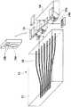
図1は、本発明の光モジュールの第1の構成例を説明するための図で、光導波路コア12とクラッド13とを備える平面型の光導波路11の端面に、複数の光半導体素子15を備えたサブキャリア(光素子搭載基台)14を設けることで光モジュールが構成され、光半導体素子15としてはPDを用い、これらのPDを、光導波路11に光結合させて8チャンネルのPDモジュールとした場合の一部を示したものである。
【0017】
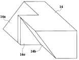
本発明の光モジュールの光素子である光半導体素子15の固定には、図中に示されているような構造のサブキャリア14が用いられる。すなわち、このサブキャリア14の光導波路11側には、垂直面に対する傾斜角が互いに反対となるように上側反射面14aと下側反射面14bとが交互に設けられ、サブキャリア14の上下面には各反射面に対応する光半導体素子15が配置されている。サブキャリア14の各反射面の反射光軸とこの反射面に対応する光半導体素子15の受光面15aとを一致させ、光半導体素子15の電気パッド15bをサブキャリア14の上面および下面に半田で固定する。光導波路11に設けられた光導波路コア12から出射した光は各々の反射面で上側または下側に反射され、各反射面に対応して配置された光半導体素子15によって受光される。なお、図示はしないが、サブキャリア14には光半導体素子15駆動用の電気配線が設けられている。
【0018】
本実施例のサブキャリア14はセラミック製であり、各反射面はセラミック材料を型押形成して得られたものであり、その形成精度は50ミクロン程度である。サブキャリア14をセラミック製としたことにより、サブキャリア表面への無電界メッキによる金属膜形成が容易となり、本実施例の反射面自体も金メッキされて形成されて得られたものである。なお、このような反射面を電気配線として用いることも可能となる。
【0019】
本実施例に示した光モジュールのクロストークは、図5に示した従来の構成の光モジュールでは−25dBであったものが、−40dBにまで低減する。また、従来の光モジュール構成における4チャンネル相当のスペースに、8チャンネルのPDを集積化することが容易に可能となる。なお、このような光モジュール構成は面型発光素子にも適用可能である。また、サブキャリア材料はセラミックスに限定されるものではなく、より成形容易なプラスチックでもよい。さらに、図1には、PD動作用のアンプ用ICなどは記載されていないが、そのようなICなどを上述のサブキャリアに配置するようにしてもよいし、それらを別の基板上に設けてサブキャリアに備えられたPDと接続するようにしてもよい。ここで、PDはサブキャリアの上面と下面の両面に取付けられているので、両面実装のプリント基板との整合もよいことがわかる。また、本実施例においては傾斜した面に反射膜を設けて反射面とする構成としたが、反射膜の替わりに誘電体多層膜を設けてフィルタとして利用してもよい。
【0020】
また、光導波路11とサブキャリア14の各々の対向面に予め位置合わせ用のマークを設けておき、位置合わせを簡便ならしめるようにしてもよい。また、光半導体素子15相互間での光のアイソレーションが必要な場合には、図2に示すように、隣接する反射面との間に仕切板14cを設けることで、簡単に光漏れを抑制することができる。さらに、光モジュールを構成するに際しては、サブキャリア14内部に光導波路構造あるいは光ファイバを収容させるようにしてもよい。
【0021】
このように本発明の光モジュールにおいては、サブキャリア14の上面と下面の両面に光半導体素子15を配置可能とすることで高集積化を可能としている。
【0022】
(実施例2)
図3は、本発明の光モジュールの第2の構成例を説明するための図で、実施例1と同様に、光導波路コア12とクラッド13とを備える平面型の光導波路11の端面に複数の光半導体素子15を備えたサブキャリア14を設け、光半導体素子15と光導波路11とを光結合させた8チャンネルのPDモジュールとした場合の一部を示したものである。
【0023】
この光モジュールが実施例1と異なる点は、光半導体素子15を固定するサブキャリア14がガラス製であり信号光に対して透明とされ反射面(14aおよび14b)が光導波路11の光出射面側とは反対の面に設けられている点、および、光半導体素子15の固定に際しては電気配線の引き回し加工工程数を削減するために光半導体素子15として裏面入射型の面型PDを用いこの面型PDの表面の電極を直接ボンディングして他の回路に接続する構造を採用している点である。この光モジュールでは、光導波路コア12から出射された光は透明なサブキャリア14の内部を伝搬し、光導波路11の光出射面側とは反対の面に設けられた複数の反射面で光信号が振り分けられる。
【0024】
このような構成とすれば、互いに反対の傾斜角を有する反射面近傍に光導波路11を配置させる必要がなくなり、光導波路11とサブキャリア14の対向面同士を直接張り合わせてモジュール化することが可能となる。なお、光導波路11とサブキャリア14とを直接張り合わせる場合には、張り合わせ面を傾斜させて光の反射を抑制するようにしてもよい。
【0025】
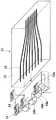
また、サブキャリア内を光が伝搬する際の光信号の放射損失を抑制するためには、図4(a)に示すようにサブキャリア14内部に光ファイバ16を配置して光信号が光ファイバ16内を伝搬するようにしてもよい。このような光ファイバ内蔵のサブキャリア14は、一方のV状に加工したファイバガイド構造(ファイバブロック)に光ファイバを整列させ、このファイバブロックと他方のファイバブロックとで上下から挟んだもので、反射面はダイシングブレードで加工され、光導波路11との張り合わせ面は予め研磨されている。なお、図4(b)に示すように、サブキャリア14に光導波路17を内蔵させ、光導波路17を形成している誘電体膜を保護するための補強板18をサブキャリア14の下部に設ける構成としても同様の効果を得ることが可能である。
【0026】
【発明の効果】
以上述べたように、本発明によれば、光半導体素子を互いに隔離することが可能となり、光および電気信号のクロストークを抑制することが可能となる。また、光半導体素子を配置する位置がサブキャリアの上下面の2面を使用することから光半導体素子の高密度な集積も可能となる。さらに、このサブキャリア中に光導波路構造を設けることにより、光結合を改善するとともに光信号の漏れを抑制することが可能となる。
【0027】
このように、本発明によれば、光素子を高密度で集積化し、かつ、光素子間の光信号および電気信号の漏れを抑制した光モジュールおよびそれを可能とするサブキャリアを提供することが可能となる。
【図面の簡単な説明】
【図1】本発明の光モジュールの第1の構成例を説明するための図である。
【図2】隣接する反射面との間に仕切りを設けたサブキャリアの構成例を説明するための図である。
【図3】本発明の光モジュールの第2の構成例を説明するための図である。
【図4】本発明の光モジュールが備えるサブキャリアの構成を説明するための図で、(a)は光ファイバ内蔵のサブキャリアの構成例、(b)は光導波路内蔵のサブキャリアの構成例である。
【図5】光導波路基板端部に光半導体素子を搭載させた従来の光モジュールの構成を説明するための図である。
【符号の説明】
11 光導波路
12 光導波路コア
13 クラッド
14 サブキャリア
14a 上側反射面
14b 下側反射面
14c 仕切板
15 光半導体素子
15a 受光面
15b 電気パッド
16 光ファイバ
17 光導波路
18 補強板[0001]
TECHNICAL FIELD OF THE INVENTION
The present invention relates to an optical module in which optical elements are integrated at high density and in which leakage of an optical signal and an electric signal between optical elements is suppressed, and a subcarrier that enables the optical module.
[0002]
[Prior art]
In an optical module in which a planar optical waveguide and a plurality of optical semiconductor elements are integrated, there are a method of mounting the optical semiconductor element on the surface of the optical waveguide substrate and a method of mounting the optical semiconductor element at an end of the optical waveguide substrate. .
[0003]
The mounting method of mounting the optical semiconductor element on the surface of the optical waveguide substrate (see Non-Patent Document 1) makes it easy to freely set the arrangement of the optical semiconductor element with respect to the optical waveguide circuit provided on the optical waveguide substrate. In addition, while there is an advantage that a well-known surface mounting technique can be applied, there is a problem that when many optical semiconductor elements are mounted, a high yield in an integrated state is required. On the other hand, when an optical semiconductor element is mounted on an end portion of an optical waveguide substrate (for example, see Non-Patent Document 2), there are the following problems.
[0004]
FIG. 5 is a view for explaining a configuration of a conventional optical module in which an optical semiconductor element is mounted on an end portion of an optical waveguide substrate, and an end face of an
[0005]
[Non-patent document 1]
T. Hashimoto et al. , "Multichip optical hybrid integration technology with planar lightwave circuit platform", IEEE, J.M. Lightwave Technology. , Vol. 16, No. 7 (1998)
[Non-patent document 2]
Minano et al., "Structure of MT-RJ Surface-Type PD Array Module", IEICE General Conference, C-3-141, 2000.
[0006]
[Problems to be solved by the invention]
However, the
[0007]
The present invention has been made in view of such a problem, and an object of the present invention is to provide an optical module in which optical elements are integrated at a high density and leakage of an optical signal and an electric signal between the optical elements is suppressed. And to provide subcarriers that make it possible.
[0008]
[Means for Solving the Problems]
In order to achieve such an object, the present invention provides a subcarrier for mounting an optical element, wherein one end face of the subcarrier has an inclination angle with respect to a vertical plane. An upper reflection surface and a lower reflection surface are provided alternately so as to be opposite to each other, and an optical element corresponding to each of the upper reflection surface and the lower reflection surface is provided on an upper surface and a lower surface of the subcarrier. It is characterized by being provided.
[0009]
According to a second aspect of the present invention, in the subcarrier according to the first aspect, a partition plate for preventing crosstalk is provided between the upper reflecting surface and the lower reflecting surface. Features.
[0010]
According to a third aspect of the present invention, in the subcarrier according to the first or second aspect, the signal light incident from a surface opposite to the one end surface is provided inside the subcarrier on the upper reflection surface. And an optical waveguide circuit for guiding the light to each of the lower reflecting surfaces.
[0011]
According to a fourth aspect of the invention, in the subcarrier according to the third aspect, the optical waveguide circuit includes a plurality of optical fibers.
[0012]
The invention according to claim 5 is the subcarrier according to claim 3 or 4, wherein a reinforcing plate for protecting the optical waveguide circuit is provided on a lower surface of the subcarrier. And
[0013]
Further, the invention according to claim 6 is an optical module, wherein a planar optical waveguide for guiding signal light of a plurality of channels and the subcarrier according to any one of claims 1 to 5 are modularized. Wherein each of the signal lights emitted from the planar optical waveguide is arranged to be received by each of the optical elements provided on the subcarrier corresponding to the plurality of channels. .
[0014]
BEST MODE FOR CARRYING OUT THE INVENTION
Hereinafter, specific embodiments of the present invention will be described with reference to the accompanying drawings.
[0015]
In all of the following embodiments, the optical waveguide is made of silica and has a step index type core structure. Although the optical waveguide is described as being formed on a silicon substrate, the material of the optical waveguide does not need to be silica. For example, an organic material such as PMMA or silicone, a ferroelectric substance such as LiNbO3 , Si or An optical waveguide using a semiconductor such as InP may be used. Further, the structure of the optical waveguide core may be a graded index type instead of a step index type. Further, the optical waveguide substrate is not limited to silicon.
[0016]
(Example 1)
FIG. 1 is a diagram for explaining a first configuration example of an optical module according to the present invention. A plurality of
[0017]
For fixing an
[0018]
The
[0019]
The crosstalk of the optical module shown in this embodiment is reduced from -25 dB in the optical module having the conventional configuration shown in FIG. 5 to -40 dB. Further, it is possible to easily integrate an 8-channel PD in a space equivalent to 4 channels in the conventional optical module configuration. In addition, such an optical module configuration can be applied to a surface light emitting device. Further, the subcarrier material is not limited to ceramics, but may be plastic that is easier to mold. Further, although FIG. 1 does not show an IC for an amplifier for PD operation or the like, such an IC or the like may be arranged on the above-described subcarrier, or they may be provided on another substrate. May be connected to the PD provided on the subcarrier. Here, since the PD is mounted on both the upper surface and the lower surface of the subcarrier, it can be seen that the matching with the printed circuit board mounted on both sides is also good. In this embodiment, the reflection film is provided on the inclined surface to provide a reflection surface. However, a dielectric multilayer film may be provided instead of the reflection film to be used as a filter.
[0020]
Also, a mark for positioning may be provided in advance on each of the opposing surfaces of the
[0021]
As described above, in the optical module of the present invention, high integration is enabled by allowing the
[0022]
(Example 2)
FIG. 3 is a diagram for explaining a second configuration example of the optical module according to the present invention. As in the first embodiment, a plurality of optical modules are provided on the end face of a planar
[0023]
This optical module is different from the first embodiment in that the
[0024]
With such a configuration, it is not necessary to dispose the
[0025]
In order to suppress radiation loss of an optical signal when light propagates in the subcarrier, an
[0026]
【The invention's effect】
As described above, according to the present invention, optical semiconductor elements can be isolated from each other, and crosstalk between optical and electrical signals can be suppressed. In addition, since the optical semiconductor elements are disposed on the upper and lower surfaces of the subcarrier, the optical semiconductor elements can be integrated at a high density. Further, by providing an optical waveguide structure in the subcarrier, it is possible to improve optical coupling and to suppress leakage of an optical signal.
[0027]
As described above, according to the present invention, it is possible to provide an optical module in which optical elements are integrated at high density and in which leakage of an optical signal and an electric signal between optical elements is suppressed, and a subcarrier that enables the optical module. It becomes possible.
[Brief description of the drawings]
FIG. 1 is a diagram illustrating a first configuration example of an optical module according to the present invention.
FIG. 2 is a diagram for explaining a configuration example of a subcarrier provided with a partition between adjacent reflection surfaces.
FIG. 3 is a diagram for explaining a second configuration example of the optical module of the present invention.
4A and 4B are diagrams for explaining a configuration of a subcarrier included in the optical module according to the present invention, wherein FIG. 4A is a configuration example of a subcarrier with a built-in optical fiber, and FIG. 4B is a configuration example of a subcarrier with a built-in optical waveguide; It is.
FIG. 5 is a diagram for explaining a configuration of a conventional optical module in which an optical semiconductor element is mounted at an end of an optical waveguide substrate.
[Explanation of symbols]
DESCRIPTION OF
Claims (6)
Translated fromJapanese当該サブキャリアの一方の端面には、垂直面に対する傾斜角が互いに反対となるように上側反射面と下側反射面とが交互に設けられており、前記サブキャリアの上面と下面には、前記上側反射面と下側反射面の各々に対応する光素子が設けられていることを特徴とするサブキャリア。A subcarrier for mounting an optical element,
On one end surface of the subcarrier, an upper reflection surface and a lower reflection surface are provided alternately so that the inclination angles with respect to the vertical surface are opposite to each other. A subcarrier provided with an optical element corresponding to each of an upper reflecting surface and a lower reflecting surface.
Priority Applications (1)
| Application Number | Priority Date | Filing Date | Title |
|---|---|---|---|
| JP2002344441AJP3920201B2 (en) | 2002-11-27 | 2002-11-27 | Subcarrier and optical module using the same |
Applications Claiming Priority (1)
| Application Number | Priority Date | Filing Date | Title |
|---|---|---|---|
| JP2002344441AJP3920201B2 (en) | 2002-11-27 | 2002-11-27 | Subcarrier and optical module using the same |
Publications (2)
| Publication Number | Publication Date |
|---|---|
| JP2004177707Atrue JP2004177707A (en) | 2004-06-24 |
| JP3920201B2 JP3920201B2 (en) | 2007-05-30 |
Family
ID=32705928
Family Applications (1)
| Application Number | Title | Priority Date | Filing Date |
|---|---|---|---|
| JP2002344441AExpired - Fee RelatedJP3920201B2 (en) | 2002-11-27 | 2002-11-27 | Subcarrier and optical module using the same |
Country Status (1)
| Country | Link |
|---|---|
| JP (1) | JP3920201B2 (en) |
Cited By (3)
| Publication number | Priority date | Publication date | Assignee | Title |
|---|---|---|---|---|
| JP2007080735A (en)* | 2005-09-15 | 2007-03-29 | Nec Corp | Light source device and its manufacturing method, indicator device and its manufacturing method, and drive method for indicator device |
| JP2012168454A (en)* | 2011-02-16 | 2012-09-06 | Sumitomo Electric Ind Ltd | Multi-channel optical receiver |
| US12215857B2 (en) | 2020-12-24 | 2025-02-04 | Nichia Corporation | Light emitting device |
Citations (6)
| Publication number | Priority date | Publication date | Assignee | Title |
|---|---|---|---|---|
| JPH0880637A (en)* | 1994-03-29 | 1996-03-26 | Ricoh Co Ltd | LED array head |
| JPH08274355A (en)* | 1995-03-31 | 1996-10-18 | Sumitomo Electric Ind Ltd | Two-dimensional array type optical element module |
| JPH09270531A (en)* | 1996-03-29 | 1997-10-14 | Sumitomo Electric Ind Ltd | Light emitting element array assembly |
| JPH09289338A (en)* | 1996-04-20 | 1997-11-04 | Ricoh Co Ltd | LED array head |
| JPH11305082A (en)* | 1998-02-23 | 1999-11-05 | Oki Electric Ind Co Ltd | Optical coupling module |
| JP2000214351A (en)* | 1999-01-21 | 2000-08-04 | Nippon Telegr & Teleph Corp <Ntt> | Optical module mounting structure |
- 2002
- 2002-11-27JPJP2002344441Apatent/JP3920201B2/ennot_activeExpired - Fee Related
Patent Citations (6)
| Publication number | Priority date | Publication date | Assignee | Title |
|---|---|---|---|---|
| JPH0880637A (en)* | 1994-03-29 | 1996-03-26 | Ricoh Co Ltd | LED array head |
| JPH08274355A (en)* | 1995-03-31 | 1996-10-18 | Sumitomo Electric Ind Ltd | Two-dimensional array type optical element module |
| JPH09270531A (en)* | 1996-03-29 | 1997-10-14 | Sumitomo Electric Ind Ltd | Light emitting element array assembly |
| JPH09289338A (en)* | 1996-04-20 | 1997-11-04 | Ricoh Co Ltd | LED array head |
| JPH11305082A (en)* | 1998-02-23 | 1999-11-05 | Oki Electric Ind Co Ltd | Optical coupling module |
| JP2000214351A (en)* | 1999-01-21 | 2000-08-04 | Nippon Telegr & Teleph Corp <Ntt> | Optical module mounting structure |
Cited By (3)
| Publication number | Priority date | Publication date | Assignee | Title |
|---|---|---|---|---|
| JP2007080735A (en)* | 2005-09-15 | 2007-03-29 | Nec Corp | Light source device and its manufacturing method, indicator device and its manufacturing method, and drive method for indicator device |
| JP2012168454A (en)* | 2011-02-16 | 2012-09-06 | Sumitomo Electric Ind Ltd | Multi-channel optical receiver |
| US12215857B2 (en) | 2020-12-24 | 2025-02-04 | Nichia Corporation | Light emitting device |
Also Published As
| Publication number | Publication date |
|---|---|
| JP3920201B2 (en) | 2007-05-30 |
Similar Documents
| Publication | Publication Date | Title |
|---|---|---|
| JP3750649B2 (en) | Optical communication device | |
| US7046868B2 (en) | Optical waveguide transmitter-receiver module | |
| US7153037B2 (en) | Multichannel optical communications module | |
| US7044659B2 (en) | Optical communications module and method for producing the module | |
| JP4060023B2 (en) | Optical waveguide transceiver module | |
| JP2002261300A (en) | Optical receiver | |
| JP2000241642A (en) | Optical transceiver module | |
| JP2006091241A (en) | Opto-electric composite wiring component and electronic device using the same | |
| US7876984B2 (en) | Planar optical waveguide array module and method of fabricating the same | |
| US7218806B2 (en) | Multi-wavelength optical transceiver module, and multiplexer/demultiplexer using thin film filter | |
| JP2004020973A (en) | Optical communication device | |
| JP2017090680A (en) | Optical wiring connection structure and optical wiring connection method | |
| JP2008102283A (en) | Optical waveguide, optical module and method of manufacturing optical waveguide | |
| JP2003057468A (en) | Optical element, optical waveguide device, manufacturing method thereof, and opto-electric hybrid board using them | |
| US6141366A (en) | Pitch-converting substrate used in semiconductor lasermodule and semiconductor lasermodule | |
| JP5309416B2 (en) | Optical module | |
| JP4638044B2 (en) | Optical transceiver module | |
| JP3920201B2 (en) | Subcarrier and optical module using the same | |
| JPH1152198A (en) | Optical connection structure | |
| EP4194913A1 (en) | A photonic integrated chip assembly comprising a package substrate with a light conductive structure | |
| JP2005003855A (en) | Bidirectional optical communication module, optical waveguide device, and bidirectional optical communication module apparatus | |
| JP4118747B2 (en) | Optical module, optical transceiver system | |
| JP2003185888A (en) | Optical communication module | |
| US6813433B2 (en) | Method for manufacturing optical waveguide and optical waveguide device, optical waveguide device and optical waveguide, and optical communication apparatus using optical waveguide device | |
| JP2003021737A (en) | Optical coupling structure between optical waveguide and light receiving element |
Legal Events
| Date | Code | Title | Description |
|---|---|---|---|
| A621 | Written request for application examination | Free format text:JAPANESE INTERMEDIATE CODE: A621 Effective date:20050120 | |
| A977 | Report on retrieval | Free format text:JAPANESE INTERMEDIATE CODE: A971007 Effective date:20061106 | |
| A131 | Notification of reasons for refusal | Free format text:JAPANESE INTERMEDIATE CODE: A131 Effective date:20061117 | |
| A521 | Written amendment | Free format text:JAPANESE INTERMEDIATE CODE: A523 Effective date:20070115 | |
| TRDD | Decision of grant or rejection written | ||
| A01 | Written decision to grant a patent or to grant a registration (utility model) | Free format text:JAPANESE INTERMEDIATE CODE: A01 Effective date:20070206 | |
| A61 | First payment of annual fees (during grant procedure) | Free format text:JAPANESE INTERMEDIATE CODE: A61 Effective date:20070214 | |
| FPAY | Renewal fee payment (event date is renewal date of database) | Free format text:PAYMENT UNTIL: 20110223 Year of fee payment:4 | |
| FPAY | Renewal fee payment (event date is renewal date of database) | Free format text:PAYMENT UNTIL: 20110223 Year of fee payment:4 | |
| FPAY | Renewal fee payment (event date is renewal date of database) | Free format text:PAYMENT UNTIL: 20120223 Year of fee payment:5 | |
| FPAY | Renewal fee payment (event date is renewal date of database) | Free format text:PAYMENT UNTIL: 20130223 Year of fee payment:6 | |
| LAPS | Cancellation because of no payment of annual fees |