JP2004171660A - Information storage device, information storage method, and information storage program - Google Patents
Information storage device, information storage method, and information storage programDownload PDFInfo
- Publication number
- JP2004171660A JP2004171660AJP2002335779AJP2002335779AJP2004171660AJP 2004171660 AJP2004171660 AJP 2004171660AJP 2002335779 AJP2002335779 AJP 2002335779AJP 2002335779 AJP2002335779 AJP 2002335779AJP 2004171660 AJP2004171660 AJP 2004171660A
- Authority
- JP
- Japan
- Prior art keywords
- information storage
- clock
- storage device
- recharging
- charge
- Prior art date
- Legal status (The legal status is an assumption and is not a legal conclusion. Google has not performed a legal analysis and makes no representation as to the accuracy of the status listed.)
- Pending
Links
- 238000000034methodMethods0.000titleclaimsdescription40
- 230000001360synchronised effectEffects0.000claimsabstractdescription18
- 230000008569processEffects0.000claimsdescription18
- 238000009825accumulationMethods0.000claims3
- 238000012545processingMethods0.000abstractdescription24
- 230000004913activationEffects0.000description10
- 238000010586diagramMethods0.000description7
- 239000004973liquid crystal related substanceSubstances0.000description4
- 230000002093peripheral effectEffects0.000description4
- 239000011159matrix materialSubstances0.000description2
- 230000004044responseEffects0.000description2
- 238000012546transferMethods0.000description2
- 230000003796beautyEffects0.000description1
- 239000003990capacitorSubstances0.000description1
- 238000004891communicationMethods0.000description1
- 238000013461designMethods0.000description1
- 230000000694effectsEffects0.000description1
- 230000006870functionEffects0.000description1
- 230000036541healthEffects0.000description1
- 230000010365information processingEffects0.000description1
- 230000014759maintenance of locationEffects0.000description1
- 238000004519manufacturing processMethods0.000description1
- 238000012986modificationMethods0.000description1
- 230000004048modificationEffects0.000description1
- 238000012544monitoring processMethods0.000description1
- 231100000989no adverse effectToxicity0.000description1
- 230000003287optical effectEffects0.000description1
- 229920001690polydopaminePolymers0.000description1
- 238000010248power generationMethods0.000description1
- 239000004065semiconductorSubstances0.000description1
Images


Landscapes
- Dram (AREA)
Abstract
Description
Translated fromJapanese【0001】
【発明の属する技術分野】
本発明はリフレッシュと称される電荷の再充電を行う情報記憶装置、情報記憶方法、及びその情報記憶方法を実行させる情報記憶プログラムに関し、特に外部からのコマンド入力を要せずに電荷の再充電を所定のタイミングで行う様な情報記憶装置、情報記憶方法、及びその情報記憶方法を実行させる情報記憶プログラムに関する。
【0002】
【従来の技術】
パーソナルコンピュータやPDA(Personal Digital Assistance)などの電子機器は、そのシステム構成として複数のLSI(Large−Scale Integrated Circuit)を内部に配設し、それらLSIの信号の入出力や信号処理に同期クロックを用いているものが広く利用されている。一般に同期動作を行うところは、その信号の周波数に比例して全体の動作速度が決まるように構成されており、このような同期動作を行う素子としては、CPU(Central Processing Unit)やメモリなどが挙げられる。
【0003】
一方、このようなシステム内においては、大容量のデータを一時的に記憶し読み出すことのできるメインメモリが通常設けられており、記憶容量当たりの製造コストが比較的に安価であることから、DRAM(Dynamic Random Access Memory)がこのようなメインメモリに頻繁に使用されている。DRAMは、コンデンサと同様の構成で電荷を蓄える複数のセルからなるメモリバンクの各セルに、デジタルデータを対応させて電荷を充電させ、電荷の有無のパターンによりデータを記憶させることができる。DRAMのデータの読み出しは、所定のセルに充電された電荷を読み出し、増幅器により増幅した後、データとして読み出すというものである。
【0004】
ところで、上述のセルに蓄えられる電荷は、そのままアクセスされない状態(読み出されない状態)で放置される状態が続くと放電してしまい、結果として、データが破壊されてしまう。そこで全部のセルに対して、所定の時間間隔でページ(マトリクス状に構成されたセルの1列分をページと言う。)毎に充電電荷をセンスアンプなどの増幅器に読み出して増幅し、元のセルに戻すという、いわゆるリフレッシュ処理が必要となっている。DRAMはこのようなリフレッシュ処理を所定の時間間隔で繰り返すことでデータを記憶し続けることができる。
【0005】
また、リフレッシュ動作を改善することにより、メモリシステムを含む処理装置の処理能力を向上させる技術も開示されている(例えば、特許文献1。)。
【0006】
【特許文献1】
特開2002−269980号公報
【0007】
【発明が解決しようとする課題】
常に一定の動作周波数ではなく、装置の動作周波数を可変とする例も知られている。例えば、パーソナルコンピュータ、PDA、携帯電話機などの電子機器では、使用状態に応じて必要な動作だけをするように工夫されてきており、例えば待機時やスリープモードの際には、動作周波数を低く制御して低消費電力化を図り、通話時や動画像の信号処理時には動作周波数を高くして高速な演算処理を実現するシステムも増加してきている。
【0008】
このような動作周波数を可変とするシステムは、その可変な動作周波数がクロックとして供給される領域が、通常、周波数を変更してはいけない固定周波数の部分とは切り離されており、動作周波数を変化させた場合でも固定周波数で動作する領域には悪影響が現れないように構成されている。また、これらの電子装置の例えばメインメモリとして使用されるDRAMは、データを保持するためにリフレッシュ処理が必要であり、低消費電力モードであってもDRAMには電源が供給されると共にリフレッシュ処理を制御するためのリフレッシュ回路にも電源が供給される。この時、DRAMの内部に自動でリフレッシュを行う回路を導入すれば、DRAMのみに電源を供給して動作させることで自動的なリフレッシュ処理が可能であり、その場合の周辺回路は簡単で容易なものにできる。
【0009】
DRAMは一般にジャンクション温度によってリフレッシュ処理が必要となる間隔が変化することから、最適なリフレッシュ処理はその間隔が変動するものであり、適切なリフレッシュ間隔の制御によっては、電源がオフで且つDRAMの電源がオンの時の消費電力を低く抑えることができる。しかしながら、従来のDRAMでは、このような制御よりも動作の安定性の方が優先し、複雑な制御を取り入れて動作させる設計例は知られていない。リフレッシュ間隔を制御する例も知られているが、予め設定されたコマンドを発行し、DRAM側ではコマンドに基づきリフレッシュ間隔をシフトさせる形式のものが多く、数多くの拡張機能を1つの素子に盛り込もうと意図した場合では十分な信号形式やコマンド形式を割り当てるのが困難となっていた。
【0010】
そこで、本発明は、上述の技術的な課題に鑑み、動作周波数を可変とするようなシステムや電子装置に搭載されながらも最適なリフレッシュ処理が確実に実現される情報記憶装置、情報記憶方法、及び情報記憶プログラムの提供を目的とする。
【0011】
【課題を解決するための手段】
本発明の情報記憶装置は、電荷を蓄積させることでデータを記憶する複数のメモリセルを有する情報記憶装置において、前記メモリセルに対して電荷の再充電を行う処理を再充電用クロックを同期信号として用いることを特徴とする。
【0012】
本発明の情報記憶装置によれば、複数のメモリセルには電荷を蓄積させることでデータを記憶させることが可能であり、前記メモリセルに対して電荷の再充電を行う処理によってデータの保持が可能となる。専用の再充電用クロックを同期信号として用いることで、この電荷の再充電を行う処理を進行させるクロックを再充電用クロックと同期させ、再充電を行う処理を確実に制御できることになる。
【0013】
また、本発明の他の情報記憶装置は、電荷を蓄積させることでデータを記憶する複数のメモリセルを有するメモリコア部と、前記メモリコア部の動作に必要な信号を供給するメモリ制御部と、再充電用クロックが供給され前記メモリコア部の各メモリセルについての電荷の再充電が該再充電用クロックの周波数に応じて制御される再充電制御部とを有することを特徴とする。
【0014】
この情報記憶装置によれば、同様に、再充電制御部は再充電用クロックが供給され、メモリコア部の各メモリセルについての電荷の再充電が該再充電用クロックの周波数に応じて制御されることから、再充電を行う処理だけを確実に制御できることになる。
【0015】
また、本発明の情報記憶方法は、周波数が可変とされる再充電用クロックを生成する手順と、生成された前記再充電用クロックに基づいて所定のメモリセルに対して電荷の再充電を行う手順とを有することを特徴とする。
【0016】
本発明の情報記憶方法では、再充電用クロックがその周波数が可変とされる形式で生成され、その再充電用クロックを用いて所定のメモリセルに対して電荷の再充電が行われる。この前記メモリセルに対して電荷の再充電を行う処理によってデータの保持が可能となり、再充電用クロックを専用なものとさせることから再充電を行う処理だけを確実に制御できることになる。
【0017】
【発明の実施の形態】
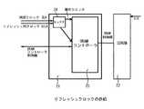
本発明の情報記憶装置の一例としてメモリ装置の例について図面を参照しながら説明する。本実施の形態のメモリ装置は、例えばSDRAM(Synchronous Dynamic Random Access Memory)若しくはDRAMコアからなるメモリ11と、その制御のためのメモリコントローラ12と、リフレッシュ用クロック生成回路13とを主な構成としている。
【0018】
メモリ11は、一例としてSDRAM即ち同期型DRAM若しくはDRAMコアからなる回路構成を有する。メモリ11がSDRAM構成の場合、例えばパーソナルコンピュータやPDAの如きシステムにおけるメモリチップがメモリ11に該当し、メモリ11がDRAMコアの場合ではマイクロコンピュータなどの記憶保持部がメモリ11に該当する。メモリ11は、後述するようにマトリクス状に配列されるセルを有しており、この各セルに電荷が充電されることでデータが記憶される。なお、メモリ11がSDRAMである場合の構成例については図4を参照しながら後述する。
【0019】
メモリ11が例えばSDRAMから構成される場合、クロック信号CLKに同期してデータについてのアクティベート動作、リード若しくはライト動作、プリチャージ動作が実行される。このクロック信号CLKは可変であっても良く、例えば10MHz、33MHz、50MHz、100MHz、133MHzなどの各周波数を切り替えて運用するようにしても良い。このメモリ11には、図1において破線で示すリフレッシュ制御部15を設けることができる。このリフレッシュ制御部15は、メモリバンクに対する信号線に信号を送るように接続されている。リフレッシュ制御部15はリフレッシュにかかるページをアクセスして電荷の再充電を行うための制御部であり、後述するようなセンスアンプと連動する。特に、本実施の形態のメモリ装置では、リフレッシュ制御部15にリフレッシュ処理専用のクロック信号であるリフレッシュ用クロック信号SCLKを入力し、リフレッシュ制御部15による電荷の再充電であるリフレッシュ間隔がリフレッシュ用クロック信号SCLKに同期して制御される。ここでリフレッシュ処理専用のクロックSCLKとは、ベースクロックやDRAMの動作クロックCLKとは別個のクロックであり、コンピュータのスリープモード、スタンバイモード、或いはソフトオフ状態の際、或いは携帯電話機の待機モードなどで通常のクロック信号CLKよりは遅い周波数に制御されることが望ましい。リフレッシュ用クロック信号SCLKが可変であっても良く、後述するように温度センサ14の出力に応じて周波数がシフトする構成とすることもできる。なお、リフレッシュ処理は、アクティベート動作とプリチャージ動作の組み合わせから実行することができる。
【0020】
DRAMコントローラ12は、メモリ11に所要の制御信号を送ってメモリ11を制御するためのデバイスである。制御信号は通常複数の信号からなり、例えばCS(チップセレクト)、RAS(ロウアドレスストローブ)、CAS(カラムアドレスストローブ)、WE(ライトイネーブル)、CKE(クロックイネーブル)、BA(バンク)、行アドレス(カラムアドレス)、列アドレス(ロウアドレス)などの各種制御信号、アドレス信号があり、これらの制御信号がメモリユニット31に入力される。この制御信号とコマンドの対応については図5に示すような関係にすることができ、これについては図5を参照しながら後述する。特にDRAMコントローラ12には、動作クロック信号CLKが供給されるが、その動作クロック信号CLKとは別個にリフレッシュ用クロック信号SCLKを供給するように構成することができる。即ち、DRAMコントローラ12がリフレッシュの制御を行う場合では、DRAMコントローラ12の一部に図1に破線で示すリフレッシュ制御部16を設け、このリフレッシュ制御部16からの制御でメモリ11がリフレッシュ処理を行うようにしても良い。具体的には、リフレッシュ制御部16には、リフレッシュ専用のリフレッシュ用クロック信号SCLKが供給され、そのリフレッシュ制御部16による電荷の再充電であるリフレッシュ間隔がリフレッシュ用クロック信号SCLKに同期して制御される。
【0021】
図1においては、それぞれ破線で示すように、メモリ11内にリフレッシュ制御部15が設けられ、DRAMコントローラ12内にリフレッシュ制御部16が形成されているが、これらのリフレッシュ制御部15、16はどちらか一方でも良く、両方設けても良い。メモリ11内に配設されるリフレッシュ制御部15は、自動的にリフレッシュ処理を行う形式、例えば内部的にリフレッシュ用のアドレス等を発生させるセルフリフレッシュ形式のものとすることができる。このような形式のリフレッシュ制御部15は、特にエンベデッドDRAMに配設する場合に好適であり、図示しないリフレッシュカウンタなどが使用される。DRAMコントローラ12内に配設されるリフレッシュ制御部16は、外部からアクティベート動作とプリチャージ動作のコマンドとそのアドレスを発生させて制御する方式の例である。
【0022】
これらのリフレッシュ制御部15、16に供給されるリフレッシュ用クロック信号SCLKはリフレッシュ用クロック生成回路13によって生成される。リフレッシュ用クロック生成回路13は、例えばパーソナルコンピュータやPDAの如きシステムの電源がオフとなっている場合でも、メモリ11のデータを保持する必要がある時には、メモリ11に対して適切な間隔でリフレッシュ処理を実行するためのリフレッシュ用クロック信号SCLKを生成させる。このリフレッシュの間隔はDRAMのリフレッシュ時間と呼ばれる電荷保持特性に左右されるが、一般的には全セルを数ms周期でアクティベート・プリチャージ動作するように制御される。
【0023】
リフレッシュ用クロック生成回路13には、メモリ周辺あるいは当該メモリ装置が搭載されるシステムの温度をモニターすることが可能な温度センサ14が接続される。一般にDRAMは温度によってリフレッシュ時間が大きく変化し、室温ではかなりリフレッシュ時間が長くなる。そこで温度を計測し、その温度に依存してリフレッシュ時間を制御するようにすれば、低消費電力化も可能である。温度センサ14は、単独のセンサーであっても良いが、CPUが把握しているシステム内の温度データを流用するようにしても良い。
【0024】
このような構成からなる本実施の形態のメモリ装置は、例えば、図2に示すような動作を行う。図2は本実施の形態のメモリ装置の動作を説明するタイムチャートであり、図2の(A)は、リフレッシュ用クロック信号SCLKと対応するDRAM内部コマンド発行方法例にかかる図であり、メモリ11のリフレッシュ動作を示す。図2の(B)はリフレッシュ用クロック信号SCLKが(A)の半分の周波数になった場合を示し、図2の(C)はリフレッシュ用クロック信号SCLKが4クロックの分散した信号とされた場合を示す。図2の(A)〜(C)において信号SCLKはリフレッシュ用クロック信号であり、コマンド(Command)信号の部分の中、”A”はアクティベート動作、”P”はプリチャージ動作のそれぞれコマンド発行の期間を示す。”Tras”はアクティベート動作からプリチャージ動作までの時間であるRASアクティベート時間を指し、リフレッシュ動作はアクティベート動作とプリチャージ動作の組み合わせで実行される。
【0025】
図2の(A)では、所定の周波数のリフレッシュ用クロック信号SCLKが供給され、そのクロック信号SCLKに応じてアクティベート動作”A”が1クロック、さらに1クロックのブランクの後、プリチャージ動作”P”が1クロック、それに連続して1クロックの合計4クロックで一回のリフレッシュ動作が進められる。このようにアクティベート動作”A”が1クロックでその後に1クロックのブランクがあるのは、RASアクティベート時間が1クロックよりも長いためである。
【0026】
例えば、パーソナルコンピュータやPDAの如きシステムの電源がオフとなり、温度センサ14が示す温度が室温程度である場合では、比較的に低速なリフレッシュ動作で十分な記憶保持動作が可能である。図2の(B)では、(A)の場合の半分の周波数のリフレッシュ用クロック信号SCLKとなっており、半分の周波数であることから、リフレッシュ用クロック信号SCLKの1クロックの周期は2倍となる。このためリフレッシュ時間が倍の期間となるが、アクティベート動作やプリチャージ動作の際に動作させる回路部分をゆっくりと動作させることで消費電流を抑えることができる。
【0027】
図2の(C)はリフレッシュ用クロック信号SCLKが4クロックの分散した信号とされた場合を示す。アクティベート動作やプリチャージ動作を低速で進める方法として、図2の(B)にリフレッシュ用クロック信号SCLKの周波数を低下させた場合について例示したが、クロックの周波数自体は変えずに間隔を空けることで実質的な周波数を下げる例である。この場合は、元のリフレッシュ用クロック信号SCLK(例えば(A)の周波数)を断続的に利用するだけで、図2の(C)のリフレッシュ用クロック信号SCLKを生成することができる。図2の(C)のリフレッシュ用クロック信号SCLKは、4クロックの集中部分が期間をあけて存在し、4クロック分を一括してリフレッシュ動作の同期に用いるように構成している。このような動作でも消費電流を抑えることができる。
【0028】
図3はリフレッシュ用のクロックの供給方法の例を示すブロック図である。メモリが同期型のSDRAM22とされ、その制御を行うDRAMコントローラ23とセレクタ24を一体化させた制御回路部21を形成している。セレクタ24には、同期クロック信号CLKとリフレッシュ用クロック信号SCLKが並行して供給されており、同期クロック信号CLKとリフレッシュ用クロック信号SCLKのどちらか一方を動作クロックとすることができるように構成されている。このセレクタ24の選択動作によって、同期クロック信号CLKが動作クロックに選ばれている場合は通常動作となるが、リフレッシュ用クロック信号SCLKが動作クロックに選ばれている場合は、SDRAM22のデータ保持だけを行う所謂セルフリフレッシュモードに自動的に切り替えられるように制御回路部21が構成される。すなわち、セレクタ24がリフレッシュ用クロック信号SCLKを動作クロックとした場合では、DRAMコントローラ23からセルフリフレッシュモードを開始させるようにDRAM制御線の信号を制御する。この制御によって、比較的に簡単な回路構成でリフレッシュ用クロック信号SCLKと同期した制御が実現されることになる。なお、セレクタは図3の例ではDRAMコントローラ23と一体化するように構成されているが、リフレッシュ用クロック生成回路側に形成するような構成でも良い。
【0029】
次に、図4を参照しながら、本実施の形態におけるSDRAMの回路構成について更に詳しく説明する。図4にはメモリコントローラ30とメモリユニット31が示されており、本実施の形態においては、メモリユニット31のリフレッシュ制御回路32にリフレッシュ用クロック信号SCLKが入力される構成となっている。リフレッシュ動作の周期は専用のリフレッシュ用クロック信号SCLKに同期するため、システムの電源オフ時においては、リフレッシュ用クロック信号SCLKの周波数を低くして、低消費電力化を図ることができる。
【0030】
メモリユニット31は、メモリバンク55と、各セルの充電された電荷を増幅させるセンスアンプ56や、その他の周辺回路から構成される。メモリバンク55は、実際にデータを記憶するものであり、複数のセル55aから構成されている。各セル55aは、コンデンサ状の構成となっており、データに対応して、各セル55aを電荷が充電された状態とするか、または、充電されない状態とすることにより、各セル55aの充電状態のパターンによりデータを記憶するものである。図4に示す例の場合、セル55aは、1個のメモリバンク55に対して8×8個設けられている例を示しているが、当然のことながら、セル55aの数は、これ以外の数であってもよい。
【0031】
また、メモリバンク55上の行毎のセル55aの集まりは、特にページ55bと呼ばれる。さらに、メモリバンク55は、リフレッシュ制御回路32のリフレッシュタイミング発生器よりリフレッシュ信号が入力されるか、または、行セレクタ53より読み出し信号が入力されると、信号が入力された行に対応するページ55b単位で、各セル55aの電荷をセンスアンプ56に転送する。尚、図4中、メモリバンク55の縦横に表示された番号(0乃至7)は、メモリバンク55の各セル55aの垂直方向の位置を示す行、および、水平方向の位置を示す例のそれぞれの番号を示している。
【0032】
センスアンプ56は、行セレクタ53により指定されたページ55bのセル55aのデータが転送されてくると、それを受け取り、さらに、所定の電位まで増幅し、再び、元のページ55bに転送する。このとき、電荷が蓄積された状態で、列セレクタ57より指定された列のデータを読み出し信号が入力されると、センスアンプ56は、指定された列のデータを読み出して、出力アンプ58に出力する。
【0033】
尚、図中、センスアンプ56は、1ページ55b分のセル55aの電荷だけしか増幅できない構成となっている。このため、リフレッシュ処理、または、読み出し処理のいずれかの1ページ分の処理だけしか処理できないので、セルフリフレッシュタイミング発生器より発生されるリフレッシュ信号、または、行セレクタ53より発生される読み出し信号は、これらの処理が、いずれかの行に対して実行されるタイミングとなるように発生されるようにCPUにより制御される。また、センスアンプ56は、複数のページ(行)に対して、リフレッシュ処理、または、読み出し処理を同時に並列処理できるよう複数に設けるようにしても良い。
【0034】
列アドレスラッチ52は、メモリコントローラ30から入力されるCAS信号を受信すると、動作状態をオンにし、メモリバンク55上のセル55aの位置を示すアドレスの列の情報を列セレクタ57に出力する。列セレクタ57は、列アドレスラッチ52より入力された列に対応するセンスアンプ56上のデータの読み出し信号をセンスアンプ56に出力し、出力アンプ58に読み出させる。出力アンプ58は、入力された電荷をさらに倍増して、メモリコントローラ30を介してCPUにデータを出力する。
【0035】
次に、CPUからの指令によりメモリコントローラ30がメモリバンク55のセル55aのデータを読み出す動作について説明する。例えば、CPUからの指令により、メモリコントローラ30がDRAMのメモリバンク55の6行4行目のセル55aのデータを読み出そうとする場合、CPUは、メモリコントローラ30に第6行第4列目のセル55aのデータを読み出すように指令する。メモリコントローラ30の制御信号発生部は、この指令を受け取ると、RAS信号を行アドレスラッチ51に出力した後、対応するアドレスの信号を行アドレスラッチ51、および、列アドレスラッチ52に出力する。行アドレスラッチ51は、RAS信号を制御信号発生部より受け取ると、その動作をオンにし、続けて受信されるアドレス情報の行の情報を行セレクタ53に出力する。従って、この場合、「第6行目」という情報が、行セレクタ53に出力される。
【0036】
行セレクタ53は、行アドレスラッチ51から入力された行の情報に基づいて、その行に対応するページ55bのセル55aの電荷をセンスアンプ56に転送させる読み出し信号を出力する。すると、今の場合、メモリバンク55上の図中実線で囲まれた第6行目のページ55bのセル55aの電荷が、センスアンプ56に出力される。センスアンプ56は、転送されてきた電荷の電荷量を所定の値まで増幅させる。
【0037】
このとき、制御信号発生部は、CAS信号を列アドレスラッチ52に出力すると共に、アドレス信号を行アドレスラッチ51、および列アドレスラッチ52に出力する。列アドレスラッチ52は、CAS信号を制御信号発生部より受け取ると、その動作をオンにし、続けて受信されるアドレス情報の列の情報を列セレクタ53に出力する。従って、図示の例の場合、「第4列目」という情報が、列セレクタ57に出力される。
【0038】
列セレクタ57は、入力された列の情報に基づいて、その列に対応するセンスアンプ56で増幅された電荷を出力アンプ58に転送させる読み出し信号を出力する。すなわち、今の場合、センスアンプ56は、この読み出し信号に基づいて、図中実線で囲まれた第4列目のセル55aの電荷が、出力アンプ58に出力される。出力アンプ58は、転送されてきた電荷の電荷量を転送に必要な所定の値まで増幅させた後、メモリコントローラ30を介してCPUにデータを出力する。尚、この後、センスアンプ56は、増幅した第6行目のページ55bの電荷を、再びメモリバンク55上の元のセル55aに戻す。従って、データの読み出しがなされた(今の場合、第6行目)ページ55b上の8個のセル55aは、充電電荷量が元の状態(フルチャージ状態)に戻されている。
【0039】
図5はSDRAMに供給される信号とコマンドの対応表の一例であり、バー記号は簡単のために省略している。CS(チップセレクト)信号が”L”(低レベル)となった時に、当該メモリユニット31が選択されている状態となる。前述の如きアクティベート動作”A”、リード動作”R”、プリチャージ動作”P”のそれぞれコマンドは、RAS(ロウアドレスストローブ)、CAS(カラムアドレスストローブ)、WE(ライトイネーブル)の組み合わせによって形成される。具体的には、RAS信号が”L”レベル、CAS信号が”H”レベル、WE信号が”H”レベルの組み合わせでアクティベート動作のコマンドが構成され、RAS信号が”H”レベル、CAS信号が”L”レベル、WE信号が”H”レベルの組み合わせでリード(読み出し)動作のコマンドが構成され、RAS信号が”H”レベル、CAS信号が”L”レベル、WE信号が”L”レベルの組み合わせでライト(書き込み)動作のコマンドが構成され、RAS信号が”L”レベル、CAS信号が”H”レベル、WE信号が”L”レベルの組み合わせでプリチャージ動作のコマンドが構成される。
【0040】
リフレッシュ処理は基本的には、アクティベート動作”A”の後にプリチャージ動作”P”を連続させることで実行される。従って、DRAMコントローラにリフレッシュ用クロック信号SCLKが供給される構成の場合では、先ず、RAS信号が”L”レベル、CAS信号が”H”レベル、WE信号が”H”レベルの組み合わせでアクティベート動作のコマンドが発行され、続いて、RAS信号が”L”レベル、CAS信号が”H”レベル、WE信号が”L”レベルの組み合わせでプリチャージ動作のコマンドが発行されて、1回のリフレッシュ動作が行われる。本実施の形態では、このアクティベート動作の後にプリチャージ動作が続くが、その切替の周期がリフレッシュ用クロック信号SCLKの周期に依存し、システムの電源オフ時においては、リフレッシュ用クロック信号SCLKの周波数を低くして、低消費電力化を図ることができる。
【0041】
次に、図6を参照しながら、本発明のメモリ装置を搭載したPDA(Personal Digital Assistance)の例について説明する。このPDAは図示しない液晶表示部やタッチパネルなどに接続されるPDAコア部60を有しており、このPDAコア部60には、所要の情報処理手順を進めるCPU61やコプロセッサ62が配設されている。CPU61はバスライン66に接続されており、このバスライン66を介して低速な回路部への接続部となるバスブリッジ67、高速な描画を実現するグラフィックエンジン63、画像の取り込みを行うカメラとの接続のためのカメラインターフェイス65、液晶表示部への信号の送受信を行うLCD(Liquid Crystal Display)コントローラ64などが接続されている。
【0042】
バスブリッジ67には、USB(Universal Serial Bus)コントローラ81、I/O用のI/Oバス82、タッチパネルインターフェイス83、キーボードやジョグダイヤル、発光ダイオードなどのインターフェイス84などの回路が接続され、更にクロック信号CLKvとその周波数情報Infqを出力する周波数制御部76もバスブリッジ67に接続されている。また、外部メモリコントローラ73は、外部メモリバスを介して接続するROM74やSDRAM75に対する制御信号を送出する回路である。
【0043】
前述のバスライン66には、更に情報記憶デバイスであるエンべデットDRAM(eDRAM)71及びDRAMコントローラ72が接続するように構成され、さらに外部メモリコントローラ73も接続する。DRAMコントローラ72は、エンべデットDRAM71に対する制御信号を送る回路部であり、特に本実施の形態では、リフレッシュ用クロック生成回路から可変とされるリフレッシュ用クロック信号SCLKが当該DRAMコントローラ72に供給される。DRAMコントローラ72はリフレッシュ用クロック信号SCLKに基づき最適なリフレッシュを行うための制御信号をエンべデットDRAM(eDRAM)71に送り、システムの電源オフ時においては、リフレッシュ用クロック信号SCLKの周波数を低くして、低消費電力化を図ることができる。
【0044】
次に、図7を参照しながら、システムをパーソナルコンピュータとした場合の実施の形態の構成について説明する。CPU(Central Processing Unit)111は、HDD(Hard Disc Drive)121に記憶されている各種アプリケーションプログラムやOS(Operating System)を実行する。ROM112は、一般的にはCPU111が使用するプログラムや演算用のパラメータのうちの基本的に固定のデータを格納する。DRAMコントローラ113は、CPU111の命令に基づいて、DRAM114を制御する。特に本実施の形態においては、クロック制御部110からクロック信号CLKとリフレッシュ用クロック信号SCLKの2つが供給され、DRAM114のリフレッシュ処理のタイミングをリフレッシュ用クロック信号SCLKの周期にあわせたものとすることができる。DRAMコントローラ113の制御信号発生部113aからDRAM114に対して所要の制御信号が出力される。
【0045】
また、CPU111はブリッジ115を介してPCI(Peripheral ComponentInterconnect)バス116に接続されている。キーボード118は、CPU111に各種の指令を入力する場合に、ユーザにより操作される。マウス119はディスプレイ120の画面上のポイントを操作するためのポンティリングデバイスであり、ディスプレイ120は液晶表示装置やCRTなどによって構成される。ドライブ131は、装着されている磁気ディスク132、光ディスク133、光磁気ディスク134、または半導体メモリ135に記憶されているデータ又はプログラムを読み出して、或いは書き込んで、そのデータ等をインターフェイス117、バス116、ブリッジ115を介してCPU111に入出力し、CPU111との間でDRAM114からの読み出し又はDRAM114への書き込みが行われる。
【0046】
この構成においても、電源がオフとなった場合では、リフレッシュ用クロック信号SCLKの周波数を低くして、リフレッシュを低速に実行して低消費電力化を図ることができる。
【0047】
なお、上述した一連の処理は、ハードウエアにより実行させることも可能であるが、ソフトウエアにより実行することも可能である。また、プログラムを記述したステップは、記載された順序に沿って時系列的に行われる処理は、必ずしも時系列的な処理に限らず並列的或いは個別的に実行される処理を含むものである。
【0048】
また、本実施の形態が搭載される電子機器もPDAやパーソナルコンピュータに限定されず、プリンターやファクシミリ、パソコン用周辺機器、電話機、テレビジョン受像機、画像表示装置、通信機器、携帯電話機、カメラ、ラジオ、オーディオビデオ機器、デジタル家電製品、照明器具、ゲーム機やラジコンカーなどの玩具、電動工具、医療機器、測定機器、車両搭載用機器、事務機器、健康美容器具、電子制御型ロボット、衣類型電子機器、各種電動機器、車両、船舶、航空機などの輸送用機械、家庭用若しくは事業用発電装置、その他の用途に使用できる種々の電子機器に搭載可能である。
【0049】
【発明の効果】
本発明の情報記憶装置によれば、リフレッシュ動作の周期は専用のリフレッシュ用クロック信号SCLKに同期するため、例えばシステムの電源オフ時においては、リフレッシュ用クロック信号SCLKの周波数を低くして、更なる低消費電力化を図ることができる。
【図面の簡単な説明】
【図1】本発明の情報記憶装置の一例を示すブロック図である。
【図2】メモリ装置の動作を説明するタイムチャートであって、(A)はリフレッシュ用クロック信号SCLKと対応するDRAM内部コマンド発行方法例を示し、(B)はリフレッシュ用クロック信号SCLKが(A)の半分の周波数になった場合を示し、(C)はリフレッシュ用クロック信号SCLKが4クロックの分散した信号とされた場合を示すそれぞれタイムチャートである。
【図3】本発明の情報記憶装置の一例においてセレクタを設けた変形例を示すブロック図である。
【図4】本発明の情報記憶装置の一例として、メモリコントローラとSDRAMを用いた場合のブロック図である。
【図5】図4のSDRAMの信号とコマンドの対応表の一例を示すテーブルである。
【図6】本発明の情報記憶装置の一例として、PDAにメモリコントローラとメモリを組み込んだ例を示すブロック図である。
【図7】本発明の情報記憶装置の一例として、パーソナルコンピュータにメモリを組み込んだ例を示すブロック図である。
【符号の説明】
11 メモリ
12 メモリコントローラ
13 リフレッシュ用クロック生成回路
14 温度センサ
15 リフレッシュ制御部
16 リフレッシュ制御部
30 メモリコントローラ
31 メモリユニット
32 リフレッシュ制御回路
61 CPU
66 バスライン
71 エンベデットDRAM
72 DRAMコントローラ
73 外部メモリコントローラ
74 ROM
75 SDRAM
SCLK リフレッシュ用クロック信号
CLK クロック信号[0001]
TECHNICAL FIELD OF THE INVENTION
The present invention relates to an information storage device, an information storage method, and an information storage program for executing the information storage method for recharging electric charges called refresh, and in particular, recharging electric charges without requiring an external command input. The present invention relates to an information storage device, an information storage method, and an information storage program for executing the information storage method for performing the information storage at a predetermined timing.
[0002]
[Prior art]
2. Description of the Related Art An electronic device such as a personal computer or a PDA (Personal Digital Assistance) has a plurality of LSIs (Large-Scale Integrated Circuits) as its system configuration, and a synchronous clock is used for input / output and signal processing of the LSIs. What is used is widely used. In general, the synchronous operation is configured such that the overall operation speed is determined in proportion to the frequency of the signal, and such a synchronous operation element includes a CPU (Central Processing Unit) and a memory. No.
[0003]
On the other hand, in such a system, a main memory capable of temporarily storing and reading a large amount of data is usually provided, and the manufacturing cost per storage capacity is relatively low. (Dynamic Random Access Memory) is frequently used for such a main memory. In a DRAM, each cell of a memory bank consisting of a plurality of cells that store electric charges in the same configuration as a capacitor is charged with electric data in correspondence with digital data, and data can be stored in a pattern of the presence or absence of electric charges. In reading data from the DRAM, charges charged in predetermined cells are read, amplified by an amplifier, and then read as data.
[0004]
By the way, the electric charge stored in the above-mentioned cell is discharged if the state where it is left as it is without being accessed (the state where it is not read out) continues, and as a result, data is destroyed. Therefore, for all the cells, the charge is read out to an amplifier such as a sense amplifier at a predetermined time interval for each page (one column of cells arranged in a matrix is called a page) and amplified, and the original charge is amplified. A so-called refresh process of returning to the cell is required. The DRAM can continue to store data by repeating such refresh processing at predetermined time intervals.
[0005]
Further, a technique for improving the processing capability of a processing device including a memory system by improving a refresh operation has been disclosed (for example, Patent Document 1).
[0006]
[Patent Document 1]
JP-A-2002-269980
[0007]
[Problems to be solved by the invention]
There is also known an example in which the operating frequency is not always constant but the operating frequency of the device is variable. For example, electronic devices such as personal computers, PDAs, and mobile phones have been devised so that only necessary operations are performed according to usage conditions. For example, in standby mode or sleep mode, the operating frequency is controlled to be low. In order to reduce power consumption and increase the frequency of operation at the time of talking and signal processing of moving images, systems for realizing high-speed arithmetic processing have been increasing.
[0008]
In such a system in which the operating frequency is variable, the region in which the variable operating frequency is supplied as a clock is usually separated from a fixed frequency portion in which the frequency must not be changed. Even if it is performed, it is configured such that no adverse effect appears in a region operating at a fixed frequency. In addition, a DRAM used as a main memory of these electronic devices, for example, requires a refresh process to retain data. Even in a low power consumption mode, power is supplied to the DRAM and the refresh process is performed. Power is also supplied to the refresh circuit for control. At this time, if a circuit for automatically refreshing is introduced into the DRAM, automatic refresh processing can be performed by supplying power only to the DRAM and operating the DRAM. In this case, peripheral circuits are simple and easy. Can be something.
[0009]
In DRAMs, the interval at which refresh processing is required generally changes depending on the junction temperature. Therefore, the optimum refresh processing varies in intervals. Depending on the appropriate control of the refresh interval, the power supply is turned off and the DRAM power supply is turned off. , The power consumption when the switch is on can be reduced. However, in the conventional DRAM, operation stability has a higher priority than such control, and there is no known design example in which the operation is performed by incorporating complicated control. An example of controlling the refresh interval is also known, but in many cases, a preset command is issued, and the DRAM side shifts the refresh interval based on the command, and many extended functions are incorporated in one element. It was difficult to assign a sufficient signal format or command format if it was intended.
[0010]
In view of the above technical problems, the present invention provides an information storage device, an information storage method, and an information storage device in which an optimal refresh process is reliably realized while being mounted on a system or an electronic device in which the operating frequency is variable. And an information storage program.
[0011]
[Means for Solving the Problems]
An information storage device according to the present invention is an information storage device having a plurality of memory cells that store data by accumulating electric charges. It is characterized by using as.
[0012]
According to the information storage device of the present invention, data can be stored by accumulating charges in a plurality of memory cells, and data can be held by a process of recharging charges in the memory cells. It becomes possible. By using the dedicated recharging clock as the synchronization signal, the clock for performing the process of recharging the charge is synchronized with the recharging clock, and the recharging process can be reliably controlled.
[0013]
Further, another information storage device of the present invention includes a memory core unit having a plurality of memory cells that store data by accumulating electric charges, and a memory control unit that supplies a signal necessary for operation of the memory core unit. A recharging control unit that is supplied with a recharging clock and controls the recharging of the electric charge of each memory cell of the memory core unit according to the frequency of the recharging clock.
[0014]
According to this information storage device, similarly, the recharging control unit is supplied with the recharging clock, and the recharging of the electric charge for each memory cell of the memory core unit is controlled according to the frequency of the recharging clock. Therefore, only the recharging process can be reliably controlled.
[0015]
According to the information storage method of the present invention, a procedure for generating a recharging clock whose frequency is variable, and recharging a predetermined memory cell based on the generated recharging clock are performed. And a procedure.
[0016]
According to the information storage method of the present invention, a recharge clock is generated in a format in which the frequency is variable, and a predetermined memory cell is recharged using the recharge clock. The data can be held by the process of recharging the charge to the memory cell, and since the recharging clock is dedicated, only the process of recharging can be reliably controlled.
[0017]
BEST MODE FOR CARRYING OUT THE INVENTION
An example of a memory device as an example of the information storage device of the present invention will be described with reference to the drawings. The memory device according to the present embodiment has, for example, a
[0018]
The
[0019]
When the
[0020]
The
[0021]
In FIG. 1, a refresh control unit 15 is provided in the
[0022]
The refresh clock signal SCLK supplied to the
[0023]
The refresh
[0024]
The memory device according to the present embodiment having such a configuration operates, for example, as shown in FIG. FIG. 2 is a time chart for explaining the operation of the memory device according to the present embodiment. FIG. 2A is a diagram relating to an example of a method of issuing a DRAM internal command corresponding to a refresh clock signal SCLK. Shows the refresh operation. FIG. 2B shows a case where the refresh clock signal SCLK has a half frequency of that of FIG. 2A, and FIG. 2C shows a case where the refresh clock signal SCLK is a dispersed signal of 4 clocks. Is shown. In FIGS. 2A to 2C, the signal SCLK is a refresh clock signal, and among the command (Command) signal portions, "A" indicates an activation operation and "P" indicates a command issuance of a precharge operation. Indicates the period. “Tras” indicates a RAS activation time that is a time from the activation operation to the precharge operation, and the refresh operation is executed by a combination of the activation operation and the precharge operation.
[0025]
In FIG. 2A, a refresh clock signal SCLK having a predetermined frequency is supplied. According to the clock signal SCLK, an activate operation “A” is performed for one clock, and after a blank of one clock, a precharge operation “P” is performed. "" Is one clock, and one refresh operation is successively performed with a total of four clocks successively. The reason why the activation operation “A” is one clock and there is a blank of one clock after that is because the RAS activation time is longer than one clock.
[0026]
For example, when the power of a system such as a personal computer or a PDA is turned off and the temperature indicated by the
[0027]
FIG. 2C shows a case where the refresh clock signal SCLK is a signal in which four clocks are dispersed. FIG. 2B illustrates a case where the frequency of the refresh clock signal SCLK is reduced as a method of performing the activate operation and the precharge operation at a low speed. This is an example of substantially lowering the frequency. In this case, the refresh clock signal SCLK of FIG. 2C can be generated only by intermittently using the original refresh clock signal SCLK (for example, the frequency of (A)). The refresh clock signal SCLK in FIG. 2C has a configuration in which a concentrated portion of four clocks exists with a period, and four clocks are collectively used for synchronization of the refresh operation. Even in such an operation, current consumption can be suppressed.
[0028]
FIG. 3 is a block diagram illustrating an example of a method of supplying a refresh clock. The memory is a
[0029]
Next, the circuit configuration of the SDRAM in the present embodiment will be described in more detail with reference to FIG. FIG. 4 shows a memory controller 30 and a memory unit 31. In the present embodiment, a refresh clock signal SCLK is input to a
[0030]
The memory unit 31 includes a memory bank 55, a
[0031]
The collection of cells 55a for each row on the memory bank 55 is particularly called a page 55b. Further, when a refresh signal is input from the refresh timing generator of the
[0032]
When the data of the cell 55a of the page 55b designated by the
[0033]
In the figure, the
[0034]
When receiving the CAS signal input from the memory controller 30, the
[0035]
Next, an operation in which the memory controller 30 reads data from the cell 55a of the memory bank 55 in response to a command from the CPU will be described. For example, when the memory controller 30 attempts to read the data of the cell 55a in the sixth row and the fourth row of the memory bank 55 of the DRAM in response to a command from the CPU, the CPU causes the memory controller 30 to read the data in the sixth row and the fourth column. To read the data of the cell 55a. Upon receiving this command, the control signal generator of the memory controller 30 outputs a RAS signal to the
[0036]
The
[0037]
At this time, the control signal generator outputs the CAS signal to the
[0038]
The
[0039]
FIG. 5 is an example of a correspondence table between signals and commands supplied to the SDRAM, and bar symbols are omitted for simplicity. When the CS (chip select) signal becomes “L” (low level), the memory unit 31 is selected. The commands of the activation operation "A", the read operation "R", and the precharge operation "P" as described above are formed by a combination of RAS (row address strobe), CAS (column address strobe), and WE (write enable). You. Specifically, the command of the activation operation is configured by a combination of the RAS signal at “L” level, the CAS signal at “H” level, and the WE signal at “H” level, and the RAS signal is at “H” level and the CAS signal is at “H” level. A read (read) operation command is configured by a combination of the “L” level and the WE signal at the “H” level. The RAS signal is at the “H” level, the CAS signal is at the “L” level, and the WE signal is at the “L” level. A combination command forms a write (write) operation command, and a combination of the RAS signal at “L” level, the CAS signal at “H” level, and the WE signal at “L” level forms a precharge operation command.
[0040]
The refresh process is basically performed by continuing the precharge operation “P” after the activate operation “A”. Therefore, in the case of the configuration in which the refresh clock signal SCLK is supplied to the DRAM controller, first, the activation operation is performed by a combination of the RAS signal at the “L” level, the CAS signal at the “H” level, and the WE signal at the “H” level. A command is issued, and then a precharge operation command is issued with a combination of the RAS signal at “L” level, the CAS signal at “H” level, and the WE signal at “L” level, and one refresh operation is performed. Done. In the present embodiment, the precharge operation follows the activate operation, but the switching cycle depends on the cycle of the refresh clock signal SCLK. When the system power is off, the frequency of the refresh clock signal SCLK is changed. By lowering the power consumption, power consumption can be reduced.
[0041]
Next, an example of a PDA (Personal Digital Assistance) equipped with the memory device of the present invention will be described with reference to FIG. The PDA has a
[0042]
The
[0043]
An embedded DRAM (eDRAM) 71 as an information storage device and a
[0044]
Next, a configuration of an embodiment in which the system is a personal computer will be described with reference to FIG. A CPU (Central Processing Unit) 111 executes various application programs and an OS (Operating System) stored in a HDD (Hard Disc Drive) 121. The
[0045]
The
[0046]
Also in this configuration, when the power supply is turned off, the frequency of the refresh clock signal SCLK is reduced, and the refresh can be performed at a low speed to reduce power consumption.
[0047]
The series of processes described above can be executed by hardware, but can also be executed by software. Further, in the steps in which the program is described, the processing performed in time series in the order described is not limited to the time-series processing, but includes processing executed in parallel or individually.
[0048]
Further, the electronic device in which the present embodiment is mounted is not limited to a PDA or a personal computer, but includes a printer, a facsimile, a peripheral device for a personal computer, a telephone, a television receiver, an image display device, a communication device, a mobile phone, a camera, Radios, audio / video equipment, digital home appliances, lighting equipment, toys such as game consoles and radio controlled cars, power tools, medical equipment, measuring equipment, equipment mounted on vehicles, office equipment, health and beauty equipment, electronically controlled robots, clothing type It can be mounted on electronic devices, various electric devices, transport machines such as vehicles, ships, aircrafts, etc., household or commercial power generation devices, and various other electronic devices that can be used for other purposes.
[0049]
【The invention's effect】
According to the information storage device of the present invention, the refresh operation cycle is synchronized with the dedicated refresh clock signal SCLK. Therefore, for example, when the power of the system is turned off, the frequency of the refresh clock signal SCLK is lowered to further increase the frequency. Low power consumption can be achieved.
[Brief description of the drawings]
FIG. 1 is a block diagram illustrating an example of an information storage device of the present invention.
FIGS. 2A and 2B are time charts for explaining the operation of a memory device, wherein FIG. 2A shows an example of a method of issuing a DRAM internal command corresponding to a refresh clock signal SCLK, and FIG. (C) is a time chart showing the case where the refresh clock signal SCLK is a dispersed signal of 4 clocks.
FIG. 3 is a block diagram showing a modification in which a selector is provided in an example of the information storage device of the present invention.
FIG. 4 is a block diagram when a memory controller and an SDRAM are used as an example of the information storage device of the present invention.
FIG. 5 is a table showing an example of a correspondence table between signals and commands of the SDRAM of FIG. 4;
FIG. 6 is a block diagram showing an example in which a memory controller and a memory are incorporated in a PDA as an example of the information storage device of the present invention.
FIG. 7 is a block diagram showing an example in which a memory is incorporated in a personal computer as an example of the information storage device of the present invention.
[Explanation of symbols]
11 Memory
12 Memory controller
13 Refresh clock generation circuit
14 Temperature sensor
15 Refresh controller
16 Refresh controller
30 Memory controller
31 memory unit
32 refresh control circuit
61 CPU
66 bus line
71 Embedded DRAM
72 DRAM controller
73 External memory controller
74 ROM
75 SDRAM
SCLK Refresh clock signal
CLK clock signal
Claims (20)
Translated fromJapanese前記メモリセルに対して電荷の再充電を行う処理を再充電用クロックを同期信号として用いることを特徴とする情報記憶装置。In an information storage device having a plurality of memory cells that store data by accumulating charges,
An information storage device, characterized in that a process for recharging the electric charge to the memory cell uses a recharging clock as a synchronization signal.
前記メモリコア部の動作に必要な信号を供給するメモリ制御部と、
再充電用クロックが供給され前記メモリコア部の各メモリセルについての電荷の再充電が該再充電用クロックの周波数に応じて制御される再充電制御部とを有することを特徴とする情報記憶装置。A memory core unit having a plurality of memory cells for storing data by accumulating electric charges,
A memory control unit that supplies a signal necessary for the operation of the memory core unit;
An information storage device, comprising: a recharge control unit that is supplied with a recharge clock and controls recharge of electric charges in each memory cell of the memory core unit in accordance with a frequency of the recharge clock. .
生成された前記再充電用クロックに基づいて所定のメモリセルに対して電荷の再充電を行う手順とを有することを特徴とする情報記憶方法。A procedure for generating a recharging clock whose frequency is variable;
Recharging a predetermined memory cell based on the generated recharging clock.
生成された前記再充電用クロックに基づいて所定のメモリセルに対して電荷の再充電を行う手順とを有する情報記憶方法を実行させることを特徴とする情報記憶プログラム。A procedure for generating a recharging clock whose frequency is variable;
Recharging a predetermined memory cell with a charge based on the generated recharge clock.
Priority Applications (1)
| Application Number | Priority Date | Filing Date | Title |
|---|---|---|---|
| JP2002335779AJP2004171660A (en) | 2002-11-19 | 2002-11-19 | Information storage device, information storage method, and information storage program |
Applications Claiming Priority (1)
| Application Number | Priority Date | Filing Date | Title |
|---|---|---|---|
| JP2002335779AJP2004171660A (en) | 2002-11-19 | 2002-11-19 | Information storage device, information storage method, and information storage program |
Publications (1)
| Publication Number | Publication Date |
|---|---|
| JP2004171660Atrue JP2004171660A (en) | 2004-06-17 |
Family
ID=32699814
Family Applications (1)
| Application Number | Title | Priority Date | Filing Date |
|---|---|---|---|
| JP2002335779APendingJP2004171660A (en) | 2002-11-19 | 2002-11-19 | Information storage device, information storage method, and information storage program |
Country Status (1)
| Country | Link |
|---|---|
| JP (1) | JP2004171660A (en) |
Cited By (3)
| Publication number | Priority date | Publication date | Assignee | Title |
|---|---|---|---|---|
| JP2006085752A (en)* | 2004-09-14 | 2006-03-30 | Matsushita Electric Ind Co Ltd | Semiconductor integrated circuit |
| JP2011044215A (en)* | 2009-08-24 | 2011-03-03 | Ricoh Co Ltd | Electronic equipment |
| EP2416229A2 (en) | 2010-08-04 | 2012-02-08 | Sony Corporation | Information processing device, power control method, and program |
Citations (10)
| Publication number | Priority date | Publication date | Assignee | Title |
|---|---|---|---|---|
| JPS63257995A (en)* | 1987-04-15 | 1988-10-25 | Toshiba Corp | Refresh control circuit |
| JPH03104083A (en)* | 1989-09-18 | 1991-05-01 | Hitachi Ltd | Refresh control method |
| JPH0550596U (en)* | 1991-12-06 | 1993-07-02 | 京セラ株式会社 | Memory backup control circuit |
| JPH07122064A (en)* | 1993-10-22 | 1995-05-12 | Toshiba Corp | Semiconductor device |
| JPH08129881A (en)* | 1994-10-31 | 1996-05-21 | Ricoh Co Ltd | SDRAM control device |
| JPH08315569A (en)* | 1995-05-16 | 1996-11-29 | Hitachi Ltd | Semiconductor memory device and data processing device |
| JPH1083669A (en)* | 1996-08-27 | 1998-03-31 | Lg Semicon Co Ltd | Refresh control circuit for semiconductor memory element |
| JPH10283774A (en)* | 1997-04-07 | 1998-10-23 | Mitsubishi Electric Corp | Clock integrated semiconductor integrated circuit device |
| JP2000235789A (en)* | 1999-02-16 | 2000-08-29 | Hitachi Ltd | Memory controller |
| JP2002133861A (en)* | 2000-10-20 | 2002-05-10 | Seiko Epson Corp | Semiconductor device, refresh method therefor, memory system and electronic device |
- 2002
- 2002-11-19JPJP2002335779Apatent/JP2004171660A/enactivePending
Patent Citations (10)
| Publication number | Priority date | Publication date | Assignee | Title |
|---|---|---|---|---|
| JPS63257995A (en)* | 1987-04-15 | 1988-10-25 | Toshiba Corp | Refresh control circuit |
| JPH03104083A (en)* | 1989-09-18 | 1991-05-01 | Hitachi Ltd | Refresh control method |
| JPH0550596U (en)* | 1991-12-06 | 1993-07-02 | 京セラ株式会社 | Memory backup control circuit |
| JPH07122064A (en)* | 1993-10-22 | 1995-05-12 | Toshiba Corp | Semiconductor device |
| JPH08129881A (en)* | 1994-10-31 | 1996-05-21 | Ricoh Co Ltd | SDRAM control device |
| JPH08315569A (en)* | 1995-05-16 | 1996-11-29 | Hitachi Ltd | Semiconductor memory device and data processing device |
| JPH1083669A (en)* | 1996-08-27 | 1998-03-31 | Lg Semicon Co Ltd | Refresh control circuit for semiconductor memory element |
| JPH10283774A (en)* | 1997-04-07 | 1998-10-23 | Mitsubishi Electric Corp | Clock integrated semiconductor integrated circuit device |
| JP2000235789A (en)* | 1999-02-16 | 2000-08-29 | Hitachi Ltd | Memory controller |
| JP2002133861A (en)* | 2000-10-20 | 2002-05-10 | Seiko Epson Corp | Semiconductor device, refresh method therefor, memory system and electronic device |
Cited By (4)
| Publication number | Priority date | Publication date | Assignee | Title |
|---|---|---|---|---|
| JP2006085752A (en)* | 2004-09-14 | 2006-03-30 | Matsushita Electric Ind Co Ltd | Semiconductor integrated circuit |
| JP2011044215A (en)* | 2009-08-24 | 2011-03-03 | Ricoh Co Ltd | Electronic equipment |
| EP2416229A2 (en) | 2010-08-04 | 2012-02-08 | Sony Corporation | Information processing device, power control method, and program |
| US9075604B2 (en) | 2010-08-04 | 2015-07-07 | Sony Corporation | Device and method for determining whether to hold data in a memory area before transitioning to a power saving state |
Similar Documents
| Publication | Publication Date | Title |
|---|---|---|
| CN101061548B (en) | Electronic system, method for refreshing DRAM unit and IC wafer | |
| US7755633B2 (en) | Loading an internal frame buffer from an external frame buffer | |
| US20040027900A1 (en) | Semiconductor memory device and system outputting refresh flag | |
| EP1351250A1 (en) | Semiconductor memory device and refresh control circuit | |
| US7793134B2 (en) | Information processing apparatus working at variable operating frequency | |
| US5119338A (en) | Memory device | |
| JP2015114777A (en) | Information processing terminal, power control program, and power control method | |
| US7330394B2 (en) | Information storage device, information storage method, and information storage program | |
| US20050235102A1 (en) | Memory controller, semiconductor integrated circuit device, microcomputer, and electronic equipment | |
| JP2004171660A (en) | Information storage device, information storage method, and information storage program | |
| JP2002352579A (en) | Information storing device and method, memory unit, recording medium, and program | |
| WO2021147043A1 (en) | Memory, controller, refresh method, and storage system | |
| US7103707B2 (en) | Access control unit and method for use with synchronous dynamic random access memory device | |
| JP2005310244A (en) | Semiconductor integrated circuit device, microcomputer and electronic device | |
| US20030043675A1 (en) | Memory system | |
| JP4096271B2 (en) | Information processing device, information storage device, information processing method, and information processing program | |
| JP2658533B2 (en) | Semiconductor storage device | |
| JPH05242671A (en) | DRAM refresh device | |
| JP2000222879A (en) | Semiconductor memory | |
| JP2845038B2 (en) | Timing control device | |
| JPH09102192A (en) | Refresh control method | |
| JP2001202777A (en) | SDRAM control device | |
| JP2019096370A (en) | Volatile memory device and self-refresh method thereof | |
| JP2014146115A (en) | Data processing device and control method thereof | |
| JP2000207882A (en) | Synchronous dram |
Legal Events
| Date | Code | Title | Description |
|---|---|---|---|
| RD04 | Notification of resignation of power of attorney | Free format text:JAPANESE INTERMEDIATE CODE: A7424 Effective date:20050530 | |
| RD02 | Notification of acceptance of power of attorney | Free format text:JAPANESE INTERMEDIATE CODE: A7422 Effective date:20050810 | |
| A621 | Written request for application examination | Free format text:JAPANESE INTERMEDIATE CODE: A621 Effective date:20051005 | |
| A977 | Report on retrieval | Free format text:JAPANESE INTERMEDIATE CODE: A971007 Effective date:20080926 | |
| A131 | Notification of reasons for refusal | Free format text:JAPANESE INTERMEDIATE CODE: A131 Effective date:20081002 | |
| A521 | Written amendment | Free format text:JAPANESE INTERMEDIATE CODE: A523 Effective date:20081127 | |
| A131 | Notification of reasons for refusal | Free format text:JAPANESE INTERMEDIATE CODE: A131 Effective date:20090602 | |
| A521 | Written amendment | Free format text:JAPANESE INTERMEDIATE CODE: A523 Effective date:20090731 | |
| A131 | Notification of reasons for refusal | Free format text:JAPANESE INTERMEDIATE CODE: A131 Effective date:20100316 | |
| A521 | Written amendment | Free format text:JAPANESE INTERMEDIATE CODE: A523 Effective date:20100510 | |
| A131 | Notification of reasons for refusal | Free format text:JAPANESE INTERMEDIATE CODE: A131 Effective date:20110215 | |
| A02 | Decision of refusal | Free format text:JAPANESE INTERMEDIATE CODE: A02 Effective date:20110630 |