JP2004163262A - Acoustic wave contact detector - Google Patents
Acoustic wave contact detectorDownload PDFInfo
- Publication number
- JP2004163262A JP2004163262AJP2002329478AJP2002329478AJP2004163262AJP 2004163262 AJP2004163262 AJP 2004163262AJP 2002329478 AJP2002329478 AJP 2002329478AJP 2002329478 AJP2002329478 AJP 2002329478AJP 2004163262 AJP2004163262 AJP 2004163262A
- Authority
- JP
- Japan
- Prior art keywords
- acoustic wave
- substrate
- lines
- fpc
- printed wirings
- Prior art date
- Legal status (The legal status is an assumption and is not a legal conclusion. Google has not performed a legal analysis and makes no representation as to the accuracy of the status listed.)
- Pending
Links
Images
Classifications
- G—PHYSICS
- G06—COMPUTING OR CALCULATING; COUNTING
- G06F—ELECTRIC DIGITAL DATA PROCESSING
- G06F3/00—Input arrangements for transferring data to be processed into a form capable of being handled by the computer; Output arrangements for transferring data from processing unit to output unit, e.g. interface arrangements
- G06F3/01—Input arrangements or combined input and output arrangements for interaction between user and computer
- G06F3/03—Arrangements for converting the position or the displacement of a member into a coded form
- G06F3/041—Digitisers, e.g. for touch screens or touch pads, characterised by the transducing means
- G—PHYSICS
- G06—COMPUTING OR CALCULATING; COUNTING
- G06F—ELECTRIC DIGITAL DATA PROCESSING
- G06F3/00—Input arrangements for transferring data to be processed into a form capable of being handled by the computer; Output arrangements for transferring data from processing unit to output unit, e.g. interface arrangements
- G06F3/01—Input arrangements or combined input and output arrangements for interaction between user and computer
- G06F3/03—Arrangements for converting the position or the displacement of a member into a coded form
- G—PHYSICS
- G01—MEASURING; TESTING
- G01B—MEASURING LENGTH, THICKNESS OR SIMILAR LINEAR DIMENSIONS; MEASURING ANGLES; MEASURING AREAS; MEASURING IRREGULARITIES OF SURFACES OR CONTOURS
- G01B17/00—Measuring arrangements characterised by the use of infrasonic, sonic or ultrasonic vibrations
- G—PHYSICS
- G06—COMPUTING OR CALCULATING; COUNTING
- G06F—ELECTRIC DIGITAL DATA PROCESSING
- G06F3/00—Input arrangements for transferring data to be processed into a form capable of being handled by the computer; Output arrangements for transferring data from processing unit to output unit, e.g. interface arrangements
- G06F3/01—Input arrangements or combined input and output arrangements for interaction between user and computer
- G06F3/03—Arrangements for converting the position or the displacement of a member into a coded form
- G06F3/041—Digitisers, e.g. for touch screens or touch pads, characterised by the transducing means
- G06F3/043—Digitisers, e.g. for touch screens or touch pads, characterised by the transducing means using propagating acoustic waves
- G06F3/0436—Digitisers, e.g. for touch screens or touch pads, characterised by the transducing means using propagating acoustic waves in which generating transducers and detecting transducers are attached to a single acoustic waves transmission substrate
- H—ELECTRICITY
- H05—ELECTRIC TECHNIQUES NOT OTHERWISE PROVIDED FOR
- H05K—PRINTED CIRCUITS; CASINGS OR CONSTRUCTIONAL DETAILS OF ELECTRIC APPARATUS; MANUFACTURE OF ASSEMBLAGES OF ELECTRICAL COMPONENTS
- H05K1/00—Printed circuits
- H05K1/02—Details
- H05K1/0213—Electrical arrangements not otherwise provided for
- H05K1/0216—Reduction of cross-talk, noise or electromagnetic interference
- H05K1/0218—Reduction of cross-talk, noise or electromagnetic interference by printed shielding conductors, ground planes or power plane
- H05K1/0219—Printed shielding conductors for shielding around or between signal conductors, e.g. coplanar or coaxial printed shielding conductors
- H—ELECTRICITY
- H05—ELECTRIC TECHNIQUES NOT OTHERWISE PROVIDED FOR
- H05K—PRINTED CIRCUITS; CASINGS OR CONSTRUCTIONAL DETAILS OF ELECTRIC APPARATUS; MANUFACTURE OF ASSEMBLAGES OF ELECTRICAL COMPONENTS
- H05K1/00—Printed circuits
- H05K1/18—Printed circuits structurally associated with non-printed electric components
- H05K1/189—Printed circuits structurally associated with non-printed electric components characterised by the use of a flexible or folded printed circuit
- H—ELECTRICITY
- H05—ELECTRIC TECHNIQUES NOT OTHERWISE PROVIDED FOR
- H05K—PRINTED CIRCUITS; CASINGS OR CONSTRUCTIONAL DETAILS OF ELECTRIC APPARATUS; MANUFACTURE OF ASSEMBLAGES OF ELECTRICAL COMPONENTS
- H05K2201/00—Indexing scheme relating to printed circuits covered by H05K1/00
- H05K2201/09—Shape and layout
- H05K2201/09209—Shape and layout details of conductors
- H05K2201/09218—Conductive traces
- H05K2201/09236—Parallel layout
Landscapes
- Engineering & Computer Science (AREA)
- Theoretical Computer Science (AREA)
- General Engineering & Computer Science (AREA)
- Physics & Mathematics (AREA)
- General Physics & Mathematics (AREA)
- Human Computer Interaction (AREA)
- Acoustics & Sound (AREA)
- Electromagnetism (AREA)
- Microelectronics & Electronic Packaging (AREA)
- Position Input By Displaying (AREA)
- Transducers For Ultrasonic Waves (AREA)
- Measurement Of Velocity Or Position Using Acoustic Or Ultrasonic Waves (AREA)
- Length Measuring Devices Characterised By Use Of Acoustic Means (AREA)
Abstract
Translated fromJapaneseDescription
Translated fromJapanese【0001】
【発明の属する技術分野】
本発明は超音波方式によるタッチパネルのような、音響的に接触位置を検出するための音響波型接触検出装置に関するものである。
【0002】
【従来の技術】
超音波による音響波型接触検出装置は、例えば、パーソナルコンピュータの操作画面、駅の切符の自動販売機、コンビニエンスストアに設置された複写機、或いは金融機関の無人端末機等に使用されている。これらの音響波型接触検出装置においては、ガラス等の基板上に配置された圧電振動子(ピエゾ素子)を含むトランスデューサが使用されている。このトランスデューサは、バルク波の発生手段として使用されるとともに、タッチパネルにタッチした指等により散乱された音響波を検出するセンサとしても使用される。そしてこれらのトランスデューサと、制御回路のコントローラを接続するのに絶縁被覆により絶縁された電線が使用されていた。
【0003】
しかし、この種の電線は断面が円形であり、基板の縁部に沿って基板上に配設したときに嵩張って、余分なスペースを必要とするという問題があった。また、基板の周縁部が、ベゼル等に覆われてスペースに余裕がない場合は、配設が困難となる場合もあった。
【0004】
また、フレキシブル基板に回路を印刷したFPC(フレキシブル印刷回路)等のフラットケーブルが用いられることもあるが、この場合には、基板上に必要とするスペースが低減される(例えば、特許文献1参照)。
【0005】
【特許文献1】
特開平6−324792号公報(第2頁、図1)
【0006】
【発明が解決しようとする課題】
基板との接続にFPCを用いた場合は、FPCに形成された信号回路(信号線)に外部電磁波が進入し易くなり、また、信号線から外部に向けて電磁波が放射されてしまうという問題がある。この理由は、FPCの信号線が外部に概ね露出した構成となっているためである。FPCの外側を金属箔等でシールド(遮蔽)すると、この問題はなくなるがFPCは高価になる。
【0007】
本願発明は、以上の点に鑑みてなされたものであり、耐EMI(電磁妨害)性に優れた安価な音響波型接触検出装置を提供することを目的とする。
【0008】
【課題を解決するための手段】
本発明の音響波型接触検出装置は、音響波が伝搬する表面を有する基板と、音響波生成手段と、生成された音響波を基板表面に沿って伝搬させる反射アレイと、表面での物体の接触による音響波の変化を検出する検出手段と、制御手段としてのコントローラとを備える音響波型接触検出装置において、音響波生成手段および検出手段の少なくとも一方とコントローラとがフレキシブル基板により接続され、フレキシブル基板は、信号線の少なくとも片側にグランド線が配置された配線パターンを有していることを特徴とする。
【0009】
また、フレキシブル基板は、信号線が複数本並列に配置された信号線群を有するとともに、信号線群の両側にグランド線が配置された配線パターンを有するよう構成することができる。
【0010】
ここでいう音響波は、基板表面上を伝搬する弾性表面波の他に、薄い基板内を基板の表面に沿って伝搬する超音波も含む。
【0011】
また、音響波生成手段はモード変換要素および超音波振動子を含むことができる。このモード変換要素は、基板に一体に形成された平行な複数本の突条から構成することができる。
【0012】
また、検出手段は、変換器とすることができる。この変換器は基板の裏面に接着される型式のものでもよく、或いは、基板表面に接着する三角柱のプリズムの一辺に接着されるウェッジ型変換器であってもよい。
【0013】
【発明の効果】
本発明の音響波型接触検出装置は、音響波生成手段および検出手段の少なくとも一方とコントローラとがフレキシブル基板により接続されている。そして、このフレキシブル基板は、信号線の少なくとも片側にグランド線が配置された配線パターンを有しているので、信号線がグランド線により電磁的にシールド(遮蔽)されて、耐EMI性に優れた音響波型接触検出装置とすることができる。また、シールドのための付加的な構造物も必要ないので、安価なものとすることができる。
【0014】
さらに、フレキシブル基板が、複数の信号線が並列に配置された信号線群を有するとともに、信号線群の両側にグランド線が配置された配線パターンを有する場合は、信号線群をまとめて効率的にシールドして耐EMI性を向上させることができる。また。これによって、フレキシブル基板を小型化できる。FPCの価格は、その面積に略比例するので、小型化により安価にすることができる。
【0015】
【発明の実施の形態】
以下、本発明の音響波型接触検出装置(以下、単に装置という)の好ましい実施の形態について、添付図面を参照して説明する。
【0016】
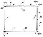
図1は、装置1に使用されるタッチパネル3の正面図である。図1に示すように、タッチパネル3は、矩形のガラス板から構成された基板2と、この基板2に取り付けられたフレキシブル基板即ちFPC(フレキシブル印刷回路)4と、このFPC4と電気的に連結された制御部(コントローラ)6から構成されている。
【0017】
FPC4は、基板2の横長方向即ち図中矢印Xで示すX軸方向に沿う分岐線4aと、X軸と直交する、矢印Yで示すY軸方向に沿う分岐線4bとに分岐している。FPC4には、超音波を発生する変換器(バルク波生成手段)8、10と、センサとなる変換器(検出手段)12、14が取り付けられている。
【0018】
また、基板2の表面即ち図1において手前側には、Y軸に沿って多数の斜めの傾斜線16からなる反射アレイ18と、この反射アレイ18に対向して、多数の傾斜線20からなる反射アレイ22が、基板2の側縁44近傍に各々形成されている。さらにX軸に沿って、基板2の上縁24近傍に多数の傾斜線26からなる反射アレイ28と、この反射アレイ28に対向して多数の傾斜線30からなる反射アレイ32が、基板2の下縁45近傍に沿って形成されている。これらの反射アレイ18、22、28、32のパターンは、特開昭61−239322号および特開2001−14094号の各公報に開示されたものである。なお反射アレイ18、22、28、32を総括して反射アレイ33という。この反射アレイ33によって音響波が反射されて、基板2の表面上を伝搬するようになっている。
【0019】
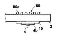
前述の変換器8、10、12、14は、基板2の裏面に接着されており、この変換器8、10、12、14に対応して、基板2の表面にモード変換要素(グレーティング)78、80、82、84が夫々形成されている。この構成について、図11を参照して、代表としてモード変換要素80を取り上げて説明する。図11は、図1の基板2を矢印A方向から見た部分概略拡大図である。図11のモード変換要素80は、ガラスペーストを焼結して基板2上に形成され、互いに離隔した平行な複数の突条80aから構成されている。図11に示す突条80aは、実際は紙面と直交方向に延びている。
【0020】
この突条80aの幅は、約400マイクロメートル、高さは、約35マイクロメートル以上になるように設定されている。この突条80aの相互の間隔を変えることによって、バルク波の反射方向が変わる。本実施形態では、突条80aの真横に表面弾性波が発生するような間隔に形成されている。このモード変換要素80の反対側には、変換器10が基板2に接着され、且つFPC4の分岐線4bとはんだ5により電気的に接続されている。
【0021】
他のモード変換要素78、82、84も、同様の構成を有している。モード変換要素78、80、82、84のうち、78、80で示すモード変換要素(音響波生成手段)は、発信側の変換器8、10から生成されたバルク波を表面弾性波に変換するものである。しかし、モード変換要素82、84は、基板2の表面を伝搬した表面弾性波(音響波)を再度バルク波に変換するものである。
【0022】
変換器10から発した約5.5MHzの超音波振動(バルク波)は、基板2の裏面から内部を通って基板2の表面にあるモード変換要素80に達すると、モード変換要素80により表面弾性波に変換されて、モード変換要素80の突条80aと直角に反射アレイ32の方向に伝搬(反射)される。そして、反射アレイ32の、内側に傾斜した多数の傾斜線30により反射され、反射アレイ28に向けて基板2の表面を伝搬し、反射アレイ28の、内側に傾斜した線26に達する。
【0023】
モード変換要素80において、100%変換されずに残った表面弾性波は、物体の検出に使用されない不要波となる。この不要波が基板2の表面を不規則に伝搬して、センサとなる変換器12、14に達すると、変換器12、14を振動させてノイズ信号を発生させることになる。
【0024】
反射アレイ28に達した表面弾性波は、さらに反射されてモード変換要素84に向けて伝搬される。モード変換要素84に達した表面弾性波は、このモード変換要素84により、バルク波に変換されて基板2の裏面にある、センサとなる受信側の変換器14にその振動が伝搬されて、変換器14により電気信号に変換される。
【0025】
変換器8から発した超音波振動(バルク波)も同様にして、モード変換要素78により表面弾性波に変換されて、反射アレイ18と反射アレイ22を経てモード変換要素82に入射される。表面弾性波はこのモード変換要素82によりバルク波に変換されてセンサとなる変換器12に伝搬され、電気信号に変換される。
【0026】
このように、表面弾性波は、反射アレイ18、22、28、32によってカバーされる基板2上の領域全てに満遍なく伝搬するので、この領域内に、例えば、指(物体)により、基板2に接触(タッチ)すると、この指により遮られた表面弾性波は、消えるか、或いは減衰する。そして、この表面弾性波の変化に伴う信号の変化は、センサとしての変換器12、14から、センサに組み合わされているコントローラ6のタイミング回路(図示せず)へ送られて、コントローラ6により、指が接触した位置の幾何学的座標が決定される。
【0027】
表面弾性波は、反射アレイ33における各傾斜線16、20、26、30の1つ1つにより反射されるが、1つの傾斜線においては到達した表面弾性波の0.5%〜1%が反射され、他は隣接する後続の傾斜線に向けて透過し、後続の傾斜線で順次反射するようになっている。
【0028】
装置1では、前述のノイズを低減するために不要波を散乱させて消去する不要波散乱手段即ち拡散格子が、基板2の表面に形成されている。この拡散格子は、図1では、34、36、38で示す矩形部分と、上縁24に沿う傾斜線40、42からなる拡散格子43および側縁44に沿う傾斜線46、48からなる拡散格子49を含む。これらの傾斜線40、42、46、48は、前述の反射アレイ18、22、28、32とは異なる機能を有する第2の反射アレイを構成している。また、拡散格子34、36、38内にも第2の反射アレイが構成されている(図7)。これらの拡散格子34、36、38、43、49についての詳細は、後述する。なお、拡散格子を総括して50で示す。
【0029】
次に、図2から図4を参照して、基板2に接着されているFPC4について説明する。図2は、基板2に接着されているFPC4を示す正面図である。FPC4は、基板2の裏面に接着されているが、図2では便宜上実線で示してある。なお、図2では、反射アレイ33および拡散格子50は省略されている。図3は、FPC4の全体を示す概略平面図である。図4は、図3においてBで示す部分を拡大したFPC4の部分拡大図である。図3および図4に示すFPC4は、図2において基板2の裏面からFPC4を見た状態と夫々対応している。
【0030】
図3および図4に示すように、FPC4は、一端に、センサとなる変換器12、14に夫々対応する電極52、54を有する。これらの電極52、54は、前述の如く、基板2に接着された変換器12、14に、上からはんだ付により接続される。即ち、変換器12、14は、FPC4と基板2の裏面との間に位置する。FPC4は、前述の分岐線4a、4bと、コントローラ6に接続される連結線4cから構成されている。
【0031】
連結線4cと分岐線4aは、同じ長さを有し、帯状に一体に形成されている(図3)。連結線4cと分岐線4aは、それらの間で長手方向に形成されたミシン目56により分離できるようになっている。分岐線4aの他端には、変換器8が接続される電極58が形成され、連結線4cの他端には、コントローラ6に連結される電極60が形成されている。また、分岐線4bの他端には、変換器10に接続される電極62が形成されている(図3)。
【0032】
図4に示すように、コントローラ6に接続される連結線4cのプリント配線64は、プリント配線64a、64b、64c、64d、64e、64f、64g、64h、64i、64jの10本が形成されている。ここで重要なことは、センサとしての変換器12、14に接続された、受信線となる4本のプリント配線64d〜64gで信号線群が構成され、この信号線群の両側にグランド(接地)用のプリント配線64c、64hが配置されている点である。
【0033】
そして、このグランド用のプリント配線64c、64hの外側には、発信用の変換器8、10に夫々接続される信号線となるプリント配線64b、64iが配置され、さらにその外側には、グランド用のプリント配線64a、64jが夫々配置されている。このことは、受信線(信号線)となるプリント配線64d〜64gが、グランド線64c、64hによって囲まれ、発信線(信号線)となるプリント配線64b、64iが、夫々グランド線64a、64cおよび64h、64jによって囲まれてシールドが形成されていることを示している。この関係は、分岐線4a、4bにおいても維持されている。これによって、プリント配線64b、64d、64e、64f、64g、64iから構成される信号線群が、外部からの電磁波の影響を受けにくくなり、また、逆に電磁波を外部に発生しにくくするという効果を奏する。上記の構成により、基板2に沿ってFPC4を配設して受信線を長く引き延ばす場合に、耐EMI性は特に効果的となる。
【0034】
なお、図中66、68で示すのは、分岐線4bの折曲線である。分岐線4bはこの折曲線66に沿って、図4における紙面の手前側に1回折り曲げられ、反対側になった電極62(図3)を変換器10に向けるため、さらに、折曲線68に沿って紙面の向こう側に折り曲げられる。この折曲部は、図2に69で示す。このようにして、分岐線4bは、基板2の側縁44に沿って配置される。なお、FPC4は、基板2に接着剤(図示せず)等により接着されて固定される。
【0035】
次に、図5に、前述の反射アレイ33のみの配置を示す。図5は、図1に示す反射アレイ33に対応する、反射アレイ33の正面図である。他の不要波散乱手段の拡散格子34、36、38等は省略してある。各反射アレイ18、22、28、32の傾斜線16、20、26、30は、45°の傾斜を有しており、表面弾性波を対向する反射アレイに向けて反射するようになっている。これらの反射アレイ33は、鉛ガラスの微粉末をペースト状にしたものをスクリーン印刷等により基板2の表面に印刷し、約500°Cで焼結して形成される。なお、図中25で基板2の隅部を部分的に示す。
【0036】
傾斜線16、20、26、30の間隔が発信側の変換器8、10から離れるに従って狭く、高密度になっているのは、傾斜線16、20、26、30を通過するに従って表面弾性波の強度が減衰するので、この減衰量を補って平均的に基板2の表面に表面弾性波が伝搬するようにするためである。なお、反射アレイ22、28は、基板2の上縁24、側縁44(図1)から僅かに内側に配置されている。この理由は、後述する、拡散格子50の傾斜線40、42、46、48が、その外側に配置できるようにするためである。
【0037】
次に、図6を参照して、不要波散乱手段となる拡散格子50について説明する。図6は、図1に対応する、拡散格子50をモード変換要素78、80、82、84とともに示す正面図である。前述の第2の反射アレイを構成する傾斜線40、42は、基板2の上縁24近傍で、互いに逆向きの角度に形成されている。そして、その角度は、基板2の中央部近傍で垂直に近く形成され、基板2の端部に行くに従って小さな角度に漸次変化している。また、第2の反射アレイを構成する他の傾斜線46、48も同様に互いに逆の傾斜を有するように形成され、且つその角度が漸次変化している。この理由は、不要波を同じ方向に反射させずに、種々の方向に拡散させる、即ち乱反射させるためである。
【0038】
これらの傾斜線40、42、46、48は、従来のテープ等が貼付されていた部分に位置している。即ち傾斜線40、42、46、48は、テープに置き換わるべく形成された部分である。この領域に達した不要波は、これらの傾斜線40、42、46、48により乱反射されて、受信側の変換器12、14に達しないようにされる。不要波は、基板2上で20cmの距離を伝搬すると、その強度は約1/10程度となる。従って、乱反射された不要波は、基板2上で反射を反復するうちに急速に減衰して消え去る。
【0039】
また、矩形の拡散格子34、36、38は、45°または−45°と異なる角度を有する、互いに離隔した突条即ち傾斜線が複数個集まって形成されている。図7および図8を参照してその形状を説明する。図7および図8は、夫々拡散格子36、38を反射アレイとともに示す部分拡大図である。図7には拡散格子36が示されており、傾斜線36aは、反射アレイ18、32の夫々の傾斜線16、30と比較して、その角度が異なっているのが明瞭に示されている。また、図8には、同様に急角度の傾斜線38aを有する拡散格子38が示されている。
【0040】
これらの拡散格子36、38も基板2の表面に伝搬する不要波を45°または−45°以外の角度で外方へ乱反射させて消去するためのものである。拡散格子34については、拡大して示さないが同様な形状および機能を有している。また、拡散格子34の傾斜線および拡散格子36、38の傾斜線36a、38aは、同じ拡散格子内で、平行であってもよいし、角度が漸次異なってもよい。拡散格子34、38は、所定の方向からそれて伝搬する表面弾性波が受信側の変換器12、14に到達する経路を断つ機能も有する。
【0041】
これらの拡散格子50は、反射アレイ33と同様に鉛ガラスの微粉末をペースト状にしたものをインクとして、基板2上に印刷されたものである。従って、反射アレイ33を形成するときに、同時に印刷することができ、生産性が向上し、製造コストも低減できる。
【0042】
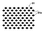
図示した拡散格子36、38の傾斜線36a、38aは、複数の突条からなるものであるが、必ずしも突条に限定されるものではなく種々の変形例が考えられる。この変形例を図9に示す。図9は、拡散格子の変形例を示す拡大図である。この拡散格子51は、平面視が菱形の多数の突起51aの集合によって構成されている。この拡散格子51に達した不要波は、これらの突起51aによって構成された領域内で、突起51a間で反射を繰り返しながら減衰するようになっている。突起の形状は、菱形に限らず、平面視が矩形、三角形等の多角形、或いは楕円等任意の形状としてよい。
【0043】
次に、図10に、基板2の表面に形成された拡散格子50と反射アレイ33の相対的な位置関係を正面図で示す。傾斜線40、42が反射アレイ28の外側に位置し、傾斜線46、48が反射アレイ22の外側に位置しているのが明瞭に示されている。拡散格子34、36、38は、反射アレイ33を反射されずに透過した音響波(表面弾性波)が、透過の直後に、反射アレイ33で反射される方向とは異なる方向へ反射されるように配置されている。
【0044】
より具体的には、例えば、変換器8およびモード変換要素78で生成された表面弾性波が、反射アレイ18を通過する間に反射アレイ22に向けて反射される。しかし、反射アレイ18で反射されずに、反射アレイ18を透過した表面弾性波は拡散格子36に達する。拡散格子36は、図7に示すように表面弾性波を基板2の外側に向けて反射させるように機能する。即ち本来の反射方向とは逆に反射させて、受信側の変換器12にノイズを生じる超音波振動が到達しないようにしている。
【0045】
また、基板2の縁部に沿って形成された拡散格子50の傾斜線40、42、46、48は、基板2の表面上を伝搬するバルク波を乱反射させて減衰させるように構成されている。通常、モード変換要素78、80によってバルク波は、表面弾性波に変換されるが、100%変換されずに残ったバルク波は、所定方向外に伝搬するので、これらの不要なバルク波を減衰させるのに使用される。
【0046】
また、モード変換要素78、80で表面弾性波に変換される際に、所定の方向からそれて伝搬する表面弾性波も、これらの傾斜線40、42、46、48によって種々の方向に離散するように乱反射される。この離散的な反射により、受信側の変換器12、14に不要な超音波振動が到達してノイズとなる虞が低減される。
【0047】
また、図10中、傾斜線40、42の間、および傾斜線46、48の間には、イルカの絵82が、傾斜線40、42、46、48と同様に印刷されているが、このような絵82もノイズ低減には有効である。これらの絵82は、外周が曲線で構成されており、この外周部分に達した、前述のバルク波、或いは表面弾性波は、様々な方向に反射されて減衰する。この図形は、外周が曲面で構成されているもの、或いは、外周に不要波を様々な方向に乱反射させる角度を有するものであれば、どのような絵であってもよいし、或いは模様であってもよい。
【0048】
以上、本発明の実施形態について詳細に説明したが、上記実施形態に限定されるものではない。例えば、拡散格子50は、フッ酸等を用いたエッチングによって形成してもよいし、或いは、レーザ、サンドブラストまたは切削等による化学的または物理的な除去加工によって形成してもよい。換言すると、突出部を形成する代わりに、溝を形成してもよい。
【0049】
また、本実施形態は、モード変換要素78、80、82、84を有する所謂グレーティングタイプの表面弾性波発生手段を用いる場合について説明したが、この実施形態に限定されるものではない。例えば、アクリル製のプリズム(図示せず)を使用した、ウェッジ型変換器(図示せず)を用いて表面弾性波を発生させる方式の音響波型接触検出装置にも適用できる。或いは、グレーティングまたはウェッジを有さない、超音波振動子上に形成された1対のくし形電極を用いた方式の音響波接触検出装置にも適用できる。
【0050】
また、本発明で使用されたFPC4は任意の接着剤で基板2に接着してよいが、圧電振動子の接着は紫外線硬化型接着剤が好ましい。この理由は、モード変換要素78、80、82、84に対する変換器8、10、12、14の微妙な仮の位置決めをして最適な表面弾性波の発生を確認した後、紫外線を照射して接着させることができるからである。
【0051】
また、不要波散乱手段は、上記に説明したように、乱反射を生ぜしめて減衰させる方式でもよい。なお、本実施形態では、2つの受信側変換器12、14が近接配置されているが、発信側変換器8、10と入れ替えて受信側変換器12、14を互いに離隔配置してもよい。この場合、一方の受信側変換器12、または14からもれた表面弾性波が、近接した位置に他方の受信側変換器14または12がないので、他方に拾われるノイズを抑制することができる。また、コントローラ6から発信側変換器8、10までの電気路を短縮できるので、この電気路からの不要輻射即ち電磁波の放射を抑制することができる。
【図面の簡単な説明】
【図1】本発明の音響波型接触検出装置に使用されるタッチパネルの正面図
【図2】基板に接着されているFPCを示す正面図
【図3】FPCの全体を示す概略平面図
【図4】図3においてBで示す部分を拡大したFPCの部分拡大図
【図5】図1に示す反射アレイに対応する、反射アレイの正面図
【図6】図1に対応する拡散格子をモード変換要素とともに示す正面図
【図7】拡散格子を反射アレイとともに示す部分拡大図
【図8】拡散格子を反射アレイとともに示す部分拡大図
【図9】拡散格子の変形例を示す拡大図
【図10】拡散格子と反射アレイの相対的な位置関係を示す正面図
【図11】図1の基板を矢印A方向から見た部分概略拡大図
【符号の説明】
1 音響波型接触検出装置
2 基板
4 フレキシブル基板(FPC)
6 コントローラ
8、10 変換器(バルク波生成手段)
12、14 変換器(検出手段)
64b、64d、64e、64f、64g、64i 信号線
64a、64c、64h、64j グランド線
78、80 モード変換要素(音響波生成手段)[0001]
BACKGROUND OF THE INVENTION
The present invention relates to an acoustic wave type contact detection device for acoustically detecting a contact position, such as an ultrasonic touch panel.
[0002]
[Prior art]
The acoustic wave type touch detection device using ultrasonic waves is used in, for example, an operation screen of a personal computer, a vending machine for a station ticket, a copying machine installed in a convenience store, or an unmanned terminal of a financial institution. In these acoustic wave type contact detection devices, a transducer including a piezoelectric vibrator (piezo element) disposed on a substrate such as glass is used. This transducer is used as a bulk wave generating means and also as a sensor for detecting an acoustic wave scattered by a finger or the like touching the touch panel. In order to connect these transducers and the controller of the control circuit, electric wires insulated by an insulating coating have been used.
[0003]
However, this type of electric wire has a circular cross section, and is bulky when disposed on the substrate along the edge of the substrate, thus requiring extra space. In addition, when the peripheral edge of the substrate is covered with a bezel or the like and there is not enough space, the arrangement may be difficult.
[0004]
In addition, a flat cable such as an FPC (flexible printed circuit) in which a circuit is printed on a flexible substrate may be used. In this case, a required space on the substrate is reduced (for example, see Patent Document 1). ).
[0005]
[Patent Document 1]
Japanese Patent Laid-Open No. 6-324792 (second page, FIG. 1)
[0006]
[Problems to be solved by the invention]
When the FPC is used for connection with the substrate, an external electromagnetic wave easily enters a signal circuit (signal line) formed on the FPC, and the electromagnetic wave is radiated from the signal line to the outside. is there. This is because the FPC signal line is generally exposed to the outside. If the outside of the FPC is shielded with a metal foil or the like, this problem is eliminated, but the FPC becomes expensive.
[0007]
This invention is made | formed in view of the above point, and it aims at providing the cheap acoustic wave type | mold contact detection apparatus excellent in EMI (electromagnetic interference) resistance.
[0008]
[Means for Solving the Problems]
The acoustic wave type contact detection apparatus of the present invention includes a substrate having a surface on which an acoustic wave propagates, an acoustic wave generating means, a reflection array for propagating the generated acoustic wave along the substrate surface, and an object on the surface. In an acoustic wave type contact detection device comprising a detection means for detecting a change in an acoustic wave due to contact and a controller as a control means, at least one of the acoustic wave generation means and the detection means and the controller are connected by a flexible substrate, and flexible The substrate has a wiring pattern in which a ground line is disposed on at least one side of a signal line.
[0009]
In addition, the flexible substrate can be configured to have a signal line group in which a plurality of signal lines are arranged in parallel, and a wiring pattern in which ground lines are arranged on both sides of the signal line group.
[0010]
The acoustic wave here includes, in addition to the surface acoustic wave propagating on the substrate surface, an ultrasonic wave propagating along the surface of the substrate in the thin substrate.
[0011]
Further, the acoustic wave generating means can include a mode conversion element and an ultrasonic transducer. This mode conversion element can be composed of a plurality of parallel protrusions integrally formed on the substrate.
[0012]
The detecting means can be a converter. This converter may be of the type that is bonded to the back surface of the substrate, or may be a wedge-type converter that is bonded to one side of a triangular prism that is bonded to the surface of the substrate.
[0013]
【The invention's effect】
In the acoustic wave type contact detection device of the present invention, at least one of the acoustic wave generation means and detection means and the controller are connected by a flexible substrate. And since this flexible substrate has a wiring pattern in which a ground line is arranged on at least one side of the signal line, the signal line is electromagnetically shielded (shielded) by the ground line and has excellent EMI resistance. It can be set as an acoustic wave type contact detection apparatus. Further, since an additional structure for shielding is not required, it can be made inexpensive.
[0014]
Further, when the flexible substrate has a signal line group in which a plurality of signal lines are arranged in parallel and has a wiring pattern in which ground lines are arranged on both sides of the signal line group, the signal line group is efficiently collected together. EMI resistance can be improved by shielding. Also. Thereby, a flexible substrate can be reduced in size. Since the price of the FPC is substantially proportional to the area, it can be made cheaper by downsizing.
[0015]
DETAILED DESCRIPTION OF THE INVENTION
Preferred embodiments of an acoustic wave type contact detection device (hereinafter simply referred to as “device”) according to the present invention will be described below with reference to the accompanying drawings.
[0016]
FIG. 1 is a front view of a
[0017]
The
[0018]
Further, on the surface of the
[0019]
The
[0020]
The
[0021]
The other
[0022]
When the ultrasonic vibration (bulk wave) of about 5.5 MHz emitted from the
[0023]
In the
[0024]
The surface acoustic wave that has reached the
[0025]
Similarly, the ultrasonic vibration (bulk wave) emitted from the
[0026]
As described above, the surface acoustic wave propagates uniformly in all the regions on the
[0027]
The surface acoustic wave is reflected by each of the
[0028]
In the apparatus 1, unnecessary wave scattering means for diffusing unnecessary waves, ie, a diffusion grating, is formed on the surface of the
[0029]
Next, the
[0030]
As shown in FIGS. 3 and 4, the
[0031]
The connecting
[0032]
As shown in FIG. 4, the printed
[0033]
The printed
[0034]
In the figure,
[0035]
Next, FIG. 5 shows an arrangement of only the
[0036]
The distance between the
[0037]
Next, with reference to FIG. 6, the diffusion grating 50 serving as unnecessary wave scattering means will be described. FIG. 6 is a front view showing the diffusion grating 50 together with the
[0038]
These
[0039]
The
[0040]
These
[0041]
These
[0042]
The
[0043]
Next, FIG. 10 is a front view showing the relative positional relationship between the diffusion grating 50 and the
[0044]
More specifically, for example, surface acoustic waves generated by the
[0045]
Further, the
[0046]
In addition, when converted into surface acoustic waves by the
[0047]
Further, in FIG. 10, a
[0048]
As mentioned above, although embodiment of this invention was described in detail, it is not limited to the said embodiment. For example, the diffusion grating 50 may be formed by etching using hydrofluoric acid or the like, or may be formed by chemical or physical removal processing such as laser, sandblasting or cutting. In other words, a groove may be formed instead of forming the protrusion.
[0049]
Moreover, although this embodiment demonstrated the case where what is called a grating type surface acoustic wave generation means which has the
[0050]
The
[0051]
Further, as described above, the unnecessary wave scattering means may be a system that causes irregular reflection to attenuate. In the present embodiment, the two receiving
[Brief description of the drawings]
FIG. 1 is a front view of a touch panel used in an acoustic wave type contact detection device of the present invention. FIG. 2 is a front view showing an FPC bonded to a substrate. FIG. 3 is a schematic plan view showing the whole FPC. 4 is a partially enlarged view of the FPC in which the portion indicated by B in FIG. 3 is enlarged. FIG. 5 is a front view of the reflecting array corresponding to the reflecting array shown in FIG. 1. FIG. 6 is a mode conversion of the diffusion grating corresponding to FIG. FIG. 7 is a partially enlarged view showing a diffusion grating together with a reflection array. FIG. 8 is a partially enlarged view showing a diffusion grating together with a reflection array. FIG. 9 is an enlarged view showing a modification of the diffusion grating. FIG. 11 is a partially enlarged schematic view of the substrate of FIG. 1 as viewed from the direction of arrow A.
DESCRIPTION OF SYMBOLS 1 Acoustic wave type
6
12, 14 Converter (detection means)
64b, 64d, 64e, 64f, 64g,
Claims (2)
Translated fromJapanese前記音響波生成手段および前記検出手段の少なくとも一方と前記コントローラとがフレキシブル基板により接続され、該フレキシブル基板は、信号線の少なくとも片側にグランド線が配置された配線パターンを有していることを特徴とする音響波型接触検出装置。A substrate having a surface on which an acoustic wave propagates; an acoustic wave generating means; a reflection array for propagating the generated acoustic wave along the substrate surface; and a change in the acoustic wave due to contact of an object on the surface. In an acoustic wave type contact detection device comprising detection means for detecting and a controller as control means,
At least one of the acoustic wave generation unit and the detection unit and the controller are connected by a flexible substrate, and the flexible substrate has a wiring pattern in which a ground line is disposed on at least one side of a signal line. An acoustic wave type contact detection device.
Priority Applications (8)
| Application Number | Priority Date | Filing Date | Title |
|---|---|---|---|
| JP2002329478AJP2004163262A (en) | 2002-11-13 | 2002-11-13 | Acoustic wave contact detector |
| AU2003301927AAU2003301927A1 (en) | 2002-11-13 | 2003-11-11 | Acoustic wave type contsct detector |
| EP03811119AEP1562104A4 (en) | 2002-11-13 | 2003-11-11 | ACOUSTIC WAVE TYPE CONTACT DETECTOR |
| CNB2003801029736ACN1327320C (en) | 2002-11-13 | 2003-11-11 | Acoustic wave type contact detection device |
| PCT/JP2003/014323WO2004044726A1 (en) | 2002-11-13 | 2003-11-11 | Acoustic wave type contsct detector |
| KR1020057008460AKR20050086550A (en) | 2002-11-13 | 2003-11-11 | Acoustic wave type contact detector |
| TW092131663ATWI291014B (en) | 2002-11-13 | 2003-11-12 | Acoustic wave touch detecting apparatus |
| US10/712,753US6948371B2 (en) | 2002-11-13 | 2003-11-12 | Acoustic wave touch detecting apparatus |
Applications Claiming Priority (1)
| Application Number | Priority Date | Filing Date | Title |
|---|---|---|---|
| JP2002329478AJP2004163262A (en) | 2002-11-13 | 2002-11-13 | Acoustic wave contact detector |
Publications (1)
| Publication Number | Publication Date |
|---|---|
| JP2004163262Atrue JP2004163262A (en) | 2004-06-10 |
Family
ID=32310570
Family Applications (1)
| Application Number | Title | Priority Date | Filing Date |
|---|---|---|---|
| JP2002329478APendingJP2004163262A (en) | 2002-11-13 | 2002-11-13 | Acoustic wave contact detector |
Country Status (8)
| Country | Link |
|---|---|
| US (1) | US6948371B2 (en) |
| EP (1) | EP1562104A4 (en) |
| JP (1) | JP2004163262A (en) |
| KR (1) | KR20050086550A (en) |
| CN (1) | CN1327320C (en) |
| AU (1) | AU2003301927A1 (en) |
| TW (1) | TWI291014B (en) |
| WO (1) | WO2004044726A1 (en) |
Cited By (4)
| Publication number | Priority date | Publication date | Assignee | Title |
|---|---|---|---|---|
| WO2005050546A3 (en)* | 2003-11-12 | 2005-10-27 | Elo Touchsystems Inc | Acoustic wave touch detecting apparatus |
| JP2010211348A (en)* | 2009-03-09 | 2010-09-24 | Hitachi Displays Ltd | Display device |
| US8253578B2 (en) | 2006-05-12 | 2012-08-28 | Panasonic Corporation | Smoke sensor of the sound wave type including a smoke density estimation unit |
| WO2024185287A1 (en)* | 2023-03-07 | 2024-09-12 | 株式会社オートネットワーク技術研究所 | Flexible substrate and wiring module |
Families Citing this family (160)
| Publication number | Priority date | Publication date | Assignee | Title |
|---|---|---|---|---|
| JP4090329B2 (en) | 2002-11-13 | 2008-05-28 | タッチパネル・システムズ株式会社 | Acoustic wave contact detector |
| TW591502B (en)* | 2003-03-11 | 2004-06-11 | Onetouch Technologies Co Ltd | Design method of the reflective streaks on ultrasonic touch screen |
| US7764276B2 (en)* | 2006-04-18 | 2010-07-27 | Schermerhorn Jerry D | Touch control system and apparatus with multiple acoustic coupled substrates |
| JP4809130B2 (en)* | 2006-05-31 | 2011-11-09 | タッチパネル・システムズ株式会社 | Acoustic wave type touch panel |
| KR101303881B1 (en)* | 2006-08-03 | 2013-09-04 | 삼성디스플레이 주식회사 | Touch screen and method of manufacturing the same, and display having the same |
| ITTV20070014A1 (en)* | 2007-02-05 | 2008-08-06 | Nice Spa | MOTOR UNIT FOR DRIVE FOR GATES |
| TWM358363U (en)* | 2009-02-05 | 2009-06-01 | Quanta Comp Inc | Optical touch sensing apparatus |
| US8336432B1 (en)* | 2011-08-19 | 2012-12-25 | David J Butler | Safety system for machine tools |
| JP5597583B2 (en)* | 2011-03-28 | 2014-10-01 | 太陽誘電株式会社 | Touch panel device and electronic device |
| US11327599B2 (en) | 2011-04-26 | 2022-05-10 | Sentons Inc. | Identifying a contact type |
| US9477350B2 (en) | 2011-04-26 | 2016-10-25 | Sentons Inc. | Method and apparatus for active ultrasonic touch devices |
| US9189109B2 (en) | 2012-07-18 | 2015-11-17 | Sentons Inc. | Detection of type of object used to provide a touch contact input |
| US9639213B2 (en) | 2011-04-26 | 2017-05-02 | Sentons Inc. | Using multiple signals to detect touch input |
| US10198097B2 (en) | 2011-04-26 | 2019-02-05 | Sentons Inc. | Detecting touch input force |
| US9348467B2 (en)* | 2011-11-15 | 2016-05-24 | Elo Touch Solutions, Inc. | Radial layout for acoustic wave touch sensor |
| US9304629B2 (en) | 2011-11-15 | 2016-04-05 | Elo Touch Solutions, Inc. | Radial transducer for acoustic wave touch sensor |
| US10248262B2 (en) | 2011-11-18 | 2019-04-02 | Sentons Inc. | User interface interaction using touch input force |
| US10235004B1 (en) | 2011-11-18 | 2019-03-19 | Sentons Inc. | Touch input detector with an integrated antenna |
| EP3627296B1 (en) | 2011-11-18 | 2021-06-23 | Sentons Inc. | Localized haptic feedback |
| US9513727B2 (en) | 2012-07-18 | 2016-12-06 | Sentons Inc. | Touch input surface microphone |
| US9348468B2 (en) | 2013-06-07 | 2016-05-24 | Sentons Inc. | Detecting multi-touch inputs |
| US9524063B2 (en) | 2012-07-18 | 2016-12-20 | Sentons Inc. | Detection of a number of touch contacts of a multi-touch input |
| US9128567B2 (en)* | 2012-11-20 | 2015-09-08 | Elo Touch Solutions, Inc. | Segmented waveguide core touch sensor systems and methods |
| US9525524B2 (en) | 2013-05-31 | 2016-12-20 | At&T Intellectual Property I, L.P. | Remote distributed antenna system |
| US9999038B2 (en) | 2013-05-31 | 2018-06-12 | At&T Intellectual Property I, L.P. | Remote distributed antenna system |
| US9588552B2 (en) | 2013-09-11 | 2017-03-07 | Sentons Inc. | Attaching electrical components using non-conductive adhesive |
| US9459715B1 (en) | 2013-09-20 | 2016-10-04 | Sentons Inc. | Using spectral control in detecting touch input |
| US9880671B2 (en) | 2013-10-08 | 2018-01-30 | Sentons Inc. | Damping vibrational wave reflections |
| US8897697B1 (en) | 2013-11-06 | 2014-11-25 | At&T Intellectual Property I, Lp | Millimeter-wave surface-wave communications |
| US9768833B2 (en) | 2014-09-15 | 2017-09-19 | At&T Intellectual Property I, L.P. | Method and apparatus for sensing a condition in a transmission medium of electromagnetic waves |
| US10063280B2 (en) | 2014-09-17 | 2018-08-28 | At&T Intellectual Property I, L.P. | Monitoring and mitigating conditions in a communication network |
| US9615269B2 (en) | 2014-10-02 | 2017-04-04 | At&T Intellectual Property I, L.P. | Method and apparatus that provides fault tolerance in a communication network |
| US9685992B2 (en) | 2014-10-03 | 2017-06-20 | At&T Intellectual Property I, L.P. | Circuit panel network and methods thereof |
| US9503189B2 (en) | 2014-10-10 | 2016-11-22 | At&T Intellectual Property I, L.P. | Method and apparatus for arranging communication sessions in a communication system |
| US9973299B2 (en) | 2014-10-14 | 2018-05-15 | At&T Intellectual Property I, L.P. | Method and apparatus for adjusting a mode of communication in a communication network |
| US9577306B2 (en) | 2014-10-21 | 2017-02-21 | At&T Intellectual Property I, L.P. | Guided-wave transmission device and methods for use therewith |
| US9780834B2 (en) | 2014-10-21 | 2017-10-03 | At&T Intellectual Property I, L.P. | Method and apparatus for transmitting electromagnetic waves |
| US9653770B2 (en) | 2014-10-21 | 2017-05-16 | At&T Intellectual Property I, L.P. | Guided wave coupler, coupling module and methods for use therewith |
| US9627768B2 (en) | 2014-10-21 | 2017-04-18 | At&T Intellectual Property I, L.P. | Guided-wave transmission device with non-fundamental mode propagation and methods for use therewith |
| US9769020B2 (en) | 2014-10-21 | 2017-09-19 | At&T Intellectual Property I, L.P. | Method and apparatus for responding to events affecting communications in a communication network |
| US9312919B1 (en) | 2014-10-21 | 2016-04-12 | At&T Intellectual Property I, Lp | Transmission device with impairment compensation and methods for use therewith |
| US9544006B2 (en) | 2014-11-20 | 2017-01-10 | At&T Intellectual Property I, L.P. | Transmission device with mode division multiplexing and methods for use therewith |
| US9742462B2 (en) | 2014-12-04 | 2017-08-22 | At&T Intellectual Property I, L.P. | Transmission medium and communication interfaces and methods for use therewith |
| US9954287B2 (en) | 2014-11-20 | 2018-04-24 | At&T Intellectual Property I, L.P. | Apparatus for converting wireless signals and electromagnetic waves and methods thereof |
| US10340573B2 (en) | 2016-10-26 | 2019-07-02 | At&T Intellectual Property I, L.P. | Launcher with cylindrical coupling device and methods for use therewith |
| US10009067B2 (en) | 2014-12-04 | 2018-06-26 | At&T Intellectual Property I, L.P. | Method and apparatus for configuring a communication interface |
| US9997819B2 (en) | 2015-06-09 | 2018-06-12 | At&T Intellectual Property I, L.P. | Transmission medium and method for facilitating propagation of electromagnetic waves via a core |
| US9800327B2 (en) | 2014-11-20 | 2017-10-24 | At&T Intellectual Property I, L.P. | Apparatus for controlling operations of a communication device and methods thereof |
| US10243784B2 (en) | 2014-11-20 | 2019-03-26 | At&T Intellectual Property I, L.P. | System for generating topology information and methods thereof |
| US9461706B1 (en) | 2015-07-31 | 2016-10-04 | At&T Intellectual Property I, Lp | Method and apparatus for exchanging communication signals |
| US9876570B2 (en) | 2015-02-20 | 2018-01-23 | At&T Intellectual Property I, Lp | Guided-wave transmission device with non-fundamental mode propagation and methods for use therewith |
| US9749013B2 (en) | 2015-03-17 | 2017-08-29 | At&T Intellectual Property I, L.P. | Method and apparatus for reducing attenuation of electromagnetic waves guided by a transmission medium |
| US10224981B2 (en) | 2015-04-24 | 2019-03-05 | At&T Intellectual Property I, Lp | Passive electrical coupling device and methods for use therewith |
| US9705561B2 (en) | 2015-04-24 | 2017-07-11 | At&T Intellectual Property I, L.P. | Directional coupling device and methods for use therewith |
| US9793954B2 (en) | 2015-04-28 | 2017-10-17 | At&T Intellectual Property I, L.P. | Magnetic coupling device and methods for use therewith |
| US9871282B2 (en) | 2015-05-14 | 2018-01-16 | At&T Intellectual Property I, L.P. | At least one transmission medium having a dielectric surface that is covered at least in part by a second dielectric |
| US9748626B2 (en) | 2015-05-14 | 2017-08-29 | At&T Intellectual Property I, L.P. | Plurality of cables having different cross-sectional shapes which are bundled together to form a transmission medium |
| US9490869B1 (en) | 2015-05-14 | 2016-11-08 | At&T Intellectual Property I, L.P. | Transmission medium having multiple cores and methods for use therewith |
| US10650940B2 (en) | 2015-05-15 | 2020-05-12 | At&T Intellectual Property I, L.P. | Transmission medium having a conductive material and methods for use therewith |
| US9917341B2 (en) | 2015-05-27 | 2018-03-13 | At&T Intellectual Property I, L.P. | Apparatus and method for launching electromagnetic waves and for modifying radial dimensions of the propagating electromagnetic waves |
| US9866309B2 (en) | 2015-06-03 | 2018-01-09 | At&T Intellectual Property I, Lp | Host node device and methods for use therewith |
| US9912381B2 (en) | 2015-06-03 | 2018-03-06 | At&T Intellectual Property I, Lp | Network termination and methods for use therewith |
| US10812174B2 (en) | 2015-06-03 | 2020-10-20 | At&T Intellectual Property I, L.P. | Client node device and methods for use therewith |
| US9913139B2 (en) | 2015-06-09 | 2018-03-06 | At&T Intellectual Property I, L.P. | Signal fingerprinting for authentication of communicating devices |
| US9820146B2 (en) | 2015-06-12 | 2017-11-14 | At&T Intellectual Property I, L.P. | Method and apparatus for authentication and identity management of communicating devices |
| US9667317B2 (en) | 2015-06-15 | 2017-05-30 | At&T Intellectual Property I, L.P. | Method and apparatus for providing security using network traffic adjustments |
| US9509415B1 (en) | 2015-06-25 | 2016-11-29 | At&T Intellectual Property I, L.P. | Methods and apparatus for inducing a fundamental wave mode on a transmission medium |
| US9865911B2 (en) | 2015-06-25 | 2018-01-09 | At&T Intellectual Property I, L.P. | Waveguide system for slot radiating first electromagnetic waves that are combined into a non-fundamental wave mode second electromagnetic wave on a transmission medium |
| US9640850B2 (en) | 2015-06-25 | 2017-05-02 | At&T Intellectual Property I, L.P. | Methods and apparatus for inducing a non-fundamental wave mode on a transmission medium |
| US9722318B2 (en) | 2015-07-14 | 2017-08-01 | At&T Intellectual Property I, L.P. | Method and apparatus for coupling an antenna to a device |
| US9847566B2 (en) | 2015-07-14 | 2017-12-19 | At&T Intellectual Property I, L.P. | Method and apparatus for adjusting a field of a signal to mitigate interference |
| US9882257B2 (en) | 2015-07-14 | 2018-01-30 | At&T Intellectual Property I, L.P. | Method and apparatus for launching a wave mode that mitigates interference |
| US10044409B2 (en) | 2015-07-14 | 2018-08-07 | At&T Intellectual Property I, L.P. | Transmission medium and methods for use therewith |
| US10148016B2 (en) | 2015-07-14 | 2018-12-04 | At&T Intellectual Property I, L.P. | Apparatus and methods for communicating utilizing an antenna array |
| US10205655B2 (en) | 2015-07-14 | 2019-02-12 | At&T Intellectual Property I, L.P. | Apparatus and methods for communicating utilizing an antenna array and multiple communication paths |
| US9853342B2 (en) | 2015-07-14 | 2017-12-26 | At&T Intellectual Property I, L.P. | Dielectric transmission medium connector and methods for use therewith |
| US10320586B2 (en) | 2015-07-14 | 2019-06-11 | At&T Intellectual Property I, L.P. | Apparatus and methods for generating non-interfering electromagnetic waves on an insulated transmission medium |
| US9628116B2 (en) | 2015-07-14 | 2017-04-18 | At&T Intellectual Property I, L.P. | Apparatus and methods for transmitting wireless signals |
| US9793951B2 (en) | 2015-07-15 | 2017-10-17 | At&T Intellectual Property I, L.P. | Method and apparatus for launching a wave mode that mitigates interference |
| US10090606B2 (en) | 2015-07-15 | 2018-10-02 | At&T Intellectual Property I, L.P. | Antenna system with dielectric array and methods for use therewith |
| US9912027B2 (en) | 2015-07-23 | 2018-03-06 | At&T Intellectual Property I, L.P. | Method and apparatus for exchanging communication signals |
| US9749053B2 (en) | 2015-07-23 | 2017-08-29 | At&T Intellectual Property I, L.P. | Node device, repeater and methods for use therewith |
| US9948333B2 (en) | 2015-07-23 | 2018-04-17 | At&T Intellectual Property I, L.P. | Method and apparatus for wireless communications to mitigate interference |
| US9871283B2 (en) | 2015-07-23 | 2018-01-16 | At&T Intellectual Property I, Lp | Transmission medium having a dielectric core comprised of plural members connected by a ball and socket configuration |
| US9967173B2 (en) | 2015-07-31 | 2018-05-08 | At&T Intellectual Property I, L.P. | Method and apparatus for authentication and identity management of communicating devices |
| US9735833B2 (en) | 2015-07-31 | 2017-08-15 | At&T Intellectual Property I, L.P. | Method and apparatus for communications management in a neighborhood network |
| US9904535B2 (en) | 2015-09-14 | 2018-02-27 | At&T Intellectual Property I, L.P. | Method and apparatus for distributing software |
| US10048811B2 (en) | 2015-09-18 | 2018-08-14 | Sentons Inc. | Detecting touch input provided by signal transmitting stylus |
| US9769128B2 (en) | 2015-09-28 | 2017-09-19 | At&T Intellectual Property I, L.P. | Method and apparatus for encryption of communications over a network |
| US9729197B2 (en) | 2015-10-01 | 2017-08-08 | At&T Intellectual Property I, L.P. | Method and apparatus for communicating network management traffic over a network |
| US9876264B2 (en) | 2015-10-02 | 2018-01-23 | At&T Intellectual Property I, Lp | Communication system, guided wave switch and methods for use therewith |
| US10355367B2 (en) | 2015-10-16 | 2019-07-16 | At&T Intellectual Property I, L.P. | Antenna structure for exchanging wireless signals |
| WO2017177408A1 (en)* | 2016-04-14 | 2017-10-19 | Abb Technology Ltd | Gripping head, gripping system and method thereof |
| US9860075B1 (en) | 2016-08-26 | 2018-01-02 | At&T Intellectual Property I, L.P. | Method and communication node for broadband distribution |
| US10340600B2 (en) | 2016-10-18 | 2019-07-02 | At&T Intellectual Property I, L.P. | Apparatus and methods for launching guided waves via plural waveguide systems |
| US10135146B2 (en) | 2016-10-18 | 2018-11-20 | At&T Intellectual Property I, L.P. | Apparatus and methods for launching guided waves via circuits |
| US10135147B2 (en) | 2016-10-18 | 2018-11-20 | At&T Intellectual Property I, L.P. | Apparatus and methods for launching guided waves via an antenna |
| US9991580B2 (en) | 2016-10-21 | 2018-06-05 | At&T Intellectual Property I, L.P. | Launcher and coupling system for guided wave mode cancellation |
| US9876605B1 (en) | 2016-10-21 | 2018-01-23 | At&T Intellectual Property I, L.P. | Launcher and coupling system to support desired guided wave mode |
| US10811767B2 (en) | 2016-10-21 | 2020-10-20 | At&T Intellectual Property I, L.P. | System and dielectric antenna with convex dielectric radome |
| US10374316B2 (en) | 2016-10-21 | 2019-08-06 | At&T Intellectual Property I, L.P. | System and dielectric antenna with non-uniform dielectric |
| US10312567B2 (en) | 2016-10-26 | 2019-06-04 | At&T Intellectual Property I, L.P. | Launcher with planar strip antenna and methods for use therewith |
| US10498044B2 (en) | 2016-11-03 | 2019-12-03 | At&T Intellectual Property I, L.P. | Apparatus for configuring a surface of an antenna |
| US10224634B2 (en) | 2016-11-03 | 2019-03-05 | At&T Intellectual Property I, L.P. | Methods and apparatus for adjusting an operational characteristic of an antenna |
| US10291334B2 (en) | 2016-11-03 | 2019-05-14 | At&T Intellectual Property I, L.P. | System for detecting a fault in a communication system |
| US10225025B2 (en) | 2016-11-03 | 2019-03-05 | At&T Intellectual Property I, L.P. | Method and apparatus for detecting a fault in a communication system |
| US10908741B2 (en) | 2016-11-10 | 2021-02-02 | Sentons Inc. | Touch input detection along device sidewall |
| US10090594B2 (en) | 2016-11-23 | 2018-10-02 | At&T Intellectual Property I, L.P. | Antenna system having structural configurations for assembly |
| US10535928B2 (en) | 2016-11-23 | 2020-01-14 | At&T Intellectual Property I, L.P. | Antenna system and methods for use therewith |
| US10178445B2 (en) | 2016-11-23 | 2019-01-08 | At&T Intellectual Property I, L.P. | Methods, devices, and systems for load balancing between a plurality of waveguides |
| US10340603B2 (en) | 2016-11-23 | 2019-07-02 | At&T Intellectual Property I, L.P. | Antenna system having shielded structural configurations for assembly |
| US10340601B2 (en) | 2016-11-23 | 2019-07-02 | At&T Intellectual Property I, L.P. | Multi-antenna system and methods for use therewith |
| US10361489B2 (en) | 2016-12-01 | 2019-07-23 | At&T Intellectual Property I, L.P. | Dielectric dish antenna system and methods for use therewith |
| US10305190B2 (en) | 2016-12-01 | 2019-05-28 | At&T Intellectual Property I, L.P. | Reflecting dielectric antenna system and methods for use therewith |
| US10326494B2 (en) | 2016-12-06 | 2019-06-18 | At&T Intellectual Property I, L.P. | Apparatus for measurement de-embedding and methods for use therewith |
| US10382976B2 (en) | 2016-12-06 | 2019-08-13 | At&T Intellectual Property I, L.P. | Method and apparatus for managing wireless communications based on communication paths and network device positions |
| US10694379B2 (en) | 2016-12-06 | 2020-06-23 | At&T Intellectual Property I, L.P. | Waveguide system with device-based authentication and methods for use therewith |
| US10819035B2 (en) | 2016-12-06 | 2020-10-27 | At&T Intellectual Property I, L.P. | Launcher with helical antenna and methods for use therewith |
| US10637149B2 (en) | 2016-12-06 | 2020-04-28 | At&T Intellectual Property I, L.P. | Injection molded dielectric antenna and methods for use therewith |
| US10727599B2 (en) | 2016-12-06 | 2020-07-28 | At&T Intellectual Property I, L.P. | Launcher with slot antenna and methods for use therewith |
| US10020844B2 (en) | 2016-12-06 | 2018-07-10 | T&T Intellectual Property I, L.P. | Method and apparatus for broadcast communication via guided waves |
| US10439675B2 (en) | 2016-12-06 | 2019-10-08 | At&T Intellectual Property I, L.P. | Method and apparatus for repeating guided wave communication signals |
| US9927517B1 (en) | 2016-12-06 | 2018-03-27 | At&T Intellectual Property I, L.P. | Apparatus and methods for sensing rainfall |
| US10755542B2 (en) | 2016-12-06 | 2020-08-25 | At&T Intellectual Property I, L.P. | Method and apparatus for surveillance via guided wave communication |
| US10135145B2 (en) | 2016-12-06 | 2018-11-20 | At&T Intellectual Property I, L.P. | Apparatus and methods for generating an electromagnetic wave along a transmission medium |
| US10243270B2 (en) | 2016-12-07 | 2019-03-26 | At&T Intellectual Property I, L.P. | Beam adaptive multi-feed dielectric antenna system and methods for use therewith |
| US10547348B2 (en) | 2016-12-07 | 2020-01-28 | At&T Intellectual Property I, L.P. | Method and apparatus for switching transmission mediums in a communication system |
| US10168695B2 (en) | 2016-12-07 | 2019-01-01 | At&T Intellectual Property I, L.P. | Method and apparatus for controlling an unmanned aircraft |
| US10139820B2 (en) | 2016-12-07 | 2018-11-27 | At&T Intellectual Property I, L.P. | Method and apparatus for deploying equipment of a communication system |
| US9893795B1 (en) | 2016-12-07 | 2018-02-13 | At&T Intellectual Property I, Lp | Method and repeater for broadband distribution |
| US10027397B2 (en) | 2016-12-07 | 2018-07-17 | At&T Intellectual Property I, L.P. | Distributed antenna system and methods for use therewith |
| US10359749B2 (en) | 2016-12-07 | 2019-07-23 | At&T Intellectual Property I, L.P. | Method and apparatus for utilities management via guided wave communication |
| US10389029B2 (en) | 2016-12-07 | 2019-08-20 | At&T Intellectual Property I, L.P. | Multi-feed dielectric antenna system with core selection and methods for use therewith |
| US10446936B2 (en) | 2016-12-07 | 2019-10-15 | At&T Intellectual Property I, L.P. | Multi-feed dielectric antenna system and methods for use therewith |
| US10136255B2 (en) | 2016-12-08 | 2018-11-20 | At&T Intellectual Property I, L.P. | Method and apparatus for proximity sensing on a communication device |
| US10103422B2 (en) | 2016-12-08 | 2018-10-16 | At&T Intellectual Property I, L.P. | Method and apparatus for mounting network devices |
| US10530505B2 (en) | 2016-12-08 | 2020-01-07 | At&T Intellectual Property I, L.P. | Apparatus and methods for launching electromagnetic waves along a transmission medium |
| US9911020B1 (en) | 2016-12-08 | 2018-03-06 | At&T Intellectual Property I, L.P. | Method and apparatus for tracking via a radio frequency identification device |
| US10326689B2 (en) | 2016-12-08 | 2019-06-18 | At&T Intellectual Property I, L.P. | Method and system for providing alternative communication paths |
| US10389037B2 (en) | 2016-12-08 | 2019-08-20 | At&T Intellectual Property I, L.P. | Apparatus and methods for selecting sections of an antenna array and use therewith |
| US10411356B2 (en) | 2016-12-08 | 2019-09-10 | At&T Intellectual Property I, L.P. | Apparatus and methods for selectively targeting communication devices with an antenna array |
| US10069535B2 (en) | 2016-12-08 | 2018-09-04 | At&T Intellectual Property I, L.P. | Apparatus and methods for launching electromagnetic waves having a certain electric field structure |
| US10938108B2 (en) | 2016-12-08 | 2021-03-02 | At&T Intellectual Property I, L.P. | Frequency selective multi-feed dielectric antenna system and methods for use therewith |
| US9998870B1 (en) | 2016-12-08 | 2018-06-12 | At&T Intellectual Property I, L.P. | Method and apparatus for proximity sensing |
| US10777873B2 (en) | 2016-12-08 | 2020-09-15 | At&T Intellectual Property I, L.P. | Method and apparatus for mounting network devices |
| US10601494B2 (en) | 2016-12-08 | 2020-03-24 | At&T Intellectual Property I, L.P. | Dual-band communication device and method for use therewith |
| US10916969B2 (en) | 2016-12-08 | 2021-02-09 | At&T Intellectual Property I, L.P. | Method and apparatus for providing power using an inductive coupling |
| US10264586B2 (en) | 2016-12-09 | 2019-04-16 | At&T Mobility Ii Llc | Cloud-based packet controller and methods for use therewith |
| US9838896B1 (en) | 2016-12-09 | 2017-12-05 | At&T Intellectual Property I, L.P. | Method and apparatus for assessing network coverage |
| US10340983B2 (en) | 2016-12-09 | 2019-07-02 | At&T Intellectual Property I, L.P. | Method and apparatus for surveying remote sites via guided wave communications |
| US10296144B2 (en) | 2016-12-12 | 2019-05-21 | Sentons Inc. | Touch input detection with shared receivers |
| US10126877B1 (en) | 2017-02-01 | 2018-11-13 | Sentons Inc. | Update of reference data for touch input detection |
| US10585522B2 (en) | 2017-02-27 | 2020-03-10 | Sentons Inc. | Detection of non-touch inputs using a signature |
| US9973940B1 (en) | 2017-02-27 | 2018-05-15 | At&T Intellectual Property I, L.P. | Apparatus and methods for dynamic impedance matching of a guided wave launcher |
| US10298293B2 (en) | 2017-03-13 | 2019-05-21 | At&T Intellectual Property I, L.P. | Apparatus of communication utilizing wireless network devices |
| EP3375408B1 (en)* | 2017-03-14 | 2019-05-15 | 3M Innovative Properties Company | Dental light polymerization device |
| US11580829B2 (en) | 2017-08-14 | 2023-02-14 | Sentons Inc. | Dynamic feedback for haptics |
| US11009411B2 (en) | 2017-08-14 | 2021-05-18 | Sentons Inc. | Increasing sensitivity of a sensor using an encoded signal |
| TWI733208B (en)* | 2019-10-03 | 2021-07-11 | 佳世達科技股份有限公司 | Ultrasonic probe and manufacturing method thereof |
| TWI692639B (en)* | 2019-10-03 | 2020-05-01 | 佳世達科技股份有限公司 | Ultrasonic probe |
Family Cites Families (10)
| Publication number | Priority date | Publication date | Assignee | Title |
|---|---|---|---|---|
| US5241308A (en)* | 1990-02-22 | 1993-08-31 | Paragon Systems, Inc. | Force sensitive touch panel |
| JPH0682301A (en)* | 1992-09-04 | 1994-03-22 | Canon Inc | Vibration detector |
| JPH09152938A (en)* | 1995-11-30 | 1997-06-10 | Sanyo Electric Co Ltd | Coordinate input incorporated display device |
| US5739479A (en)* | 1996-03-04 | 1998-04-14 | Elo Touchsystems, Inc. | Gentle-bevel flat acoustic wave touch sensor |
| TW490632B (en)* | 1996-12-25 | 2002-06-11 | Elo Touchsystems Inc | Grating transducer for acoustic touchscreen |
| JP2000043484A (en)* | 1998-07-30 | 2000-02-15 | Ricoh Co Ltd | Electronic blackboard system |
| JP4024933B2 (en)* | 1998-08-18 | 2007-12-19 | タッチパネル・システムズ株式会社 | Touch panel |
| JP3451373B2 (en)* | 1999-11-24 | 2003-09-29 | オムロン株式会社 | Manufacturing method of data carrier capable of reading electromagnetic wave |
| US6741237B1 (en)* | 2001-08-23 | 2004-05-25 | Rockwell Automation Technologies, Inc. | Touch screen |
| JP3971674B2 (en)* | 2002-07-10 | 2007-09-05 | 富士通株式会社 | Contact-type sensor built-in semiconductor device and manufacturing method thereof |
- 2002
- 2002-11-13JPJP2002329478Apatent/JP2004163262A/enactivePending
- 2003
- 2003-11-11WOPCT/JP2003/014323patent/WO2004044726A1/enactiveApplication Filing
- 2003-11-11EPEP03811119Apatent/EP1562104A4/ennot_activeCeased
- 2003-11-11KRKR1020057008460Apatent/KR20050086550A/ennot_activeCeased
- 2003-11-11CNCNB2003801029736Apatent/CN1327320C/ennot_activeExpired - Fee Related
- 2003-11-11AUAU2003301927Apatent/AU2003301927A1/ennot_activeAbandoned
- 2003-11-12TWTW092131663Apatent/TWI291014B/ennot_activeIP Right Cessation
- 2003-11-12USUS10/712,753patent/US6948371B2/ennot_activeExpired - Lifetime
Cited By (4)
| Publication number | Priority date | Publication date | Assignee | Title |
|---|---|---|---|---|
| WO2005050546A3 (en)* | 2003-11-12 | 2005-10-27 | Elo Touchsystems Inc | Acoustic wave touch detecting apparatus |
| US8253578B2 (en) | 2006-05-12 | 2012-08-28 | Panasonic Corporation | Smoke sensor of the sound wave type including a smoke density estimation unit |
| JP2010211348A (en)* | 2009-03-09 | 2010-09-24 | Hitachi Displays Ltd | Display device |
| WO2024185287A1 (en)* | 2023-03-07 | 2024-09-12 | 株式会社オートネットワーク技術研究所 | Flexible substrate and wiring module |
Also Published As
| Publication number | Publication date |
|---|---|
| AU2003301927A1 (en) | 2004-06-03 |
| CN1711518A (en) | 2005-12-21 |
| CN1327320C (en) | 2007-07-18 |
| US6948371B2 (en) | 2005-09-27 |
| EP1562104A4 (en) | 2005-11-09 |
| TW200427966A (en) | 2004-12-16 |
| KR20050086550A (en) | 2005-08-30 |
| TWI291014B (en) | 2007-12-11 |
| EP1562104A1 (en) | 2005-08-10 |
| US20050035685A1 (en) | 2005-02-17 |
| WO2004044726A1 (en) | 2004-05-27 |
Similar Documents
| Publication | Publication Date | Title |
|---|---|---|
| JP4090329B2 (en) | Acoustic wave contact detector | |
| CN1327320C (en) | Acoustic wave type contact detection device | |
| US8896564B2 (en) | Acoustic touch apparatus | |
| US7187369B1 (en) | Acoustic touch sensor | |
| JP2001014093A (en) | Acoustic contact detection device | |
| KR20110086738A (en) | Acoustic touch sensor | |
| JP2006099608A (en) | Display device with contact detection function | |
| CN100380298C (en) | Acoustic wave type touch detection device | |
| KR20070011248A (en) | Acoustic Wave Contact Detection Device |
Legal Events
| Date | Code | Title | Description |
|---|---|---|---|
| A621 | Written request for application examination | Free format text:JAPANESE INTERMEDIATE CODE: A621 Effective date:20050829 | |
| A131 | Notification of reasons for refusal | Free format text:JAPANESE INTERMEDIATE CODE: A131 Effective date:20080318 | |
| A521 | Request for written amendment filed | Free format text:JAPANESE INTERMEDIATE CODE: A523 Effective date:20080519 | |
| A02 | Decision of refusal | Free format text:JAPANESE INTERMEDIATE CODE: A02 Effective date:20080610 |