JP2004159148A - Circuit for three-dimensional representation - Google Patents
Circuit for three-dimensional representationDownload PDFInfo
- Publication number
- JP2004159148A JP2004159148AJP2002323603AJP2002323603AJP2004159148AJP 2004159148 AJP2004159148 AJP 2004159148AJP 2002323603 AJP2002323603 AJP 2002323603AJP 2002323603 AJP2002323603 AJP 2002323603AJP 2004159148 AJP2004159148 AJP 2004159148A
- Authority
- JP
- Japan
- Prior art keywords
- circuit
- output
- data
- input data
- contour
- Prior art date
- Legal status (The legal status is an assumption and is not a legal conclusion. Google has not performed a legal analysis and makes no representation as to the accuracy of the status listed.)
- Pending
Links
Images


Landscapes
- Image Processing (AREA)
- Picture Signal Circuits (AREA)
- Facsimile Image Signal Circuits (AREA)
- Controls And Circuits For Display Device (AREA)
Abstract
Translated fromJapaneseDescription
Translated fromJapanese【0001】
【発明の属する技術分野】
本発明は、ディジタル画像処理における輪郭強調処理を用いた立体的表現回路に関するものである
【0002】
【従来の技術】
従来より、PDP(プラズマ・ディスプレイ・パネル)等のディスプレイ装置に表示する画像について輪郭強調処理を行い、表示画像を立体的に表現する技術が存在する。これは、人や建物などの物体と周囲の背景との間に輪郭成分が強く現れる性質があることを利用したもので、適度に輪郭を強調することで、物体と周囲の背景とに遠近感が現れ、人の目には画像が立体的であると感じることによるものである。
【0003】
図7は、従来の立体的表現回路を示したものである。この図7において、データ入力端子10からの入力データは、遅延回路11と輪郭抽出部12に入力される。輪郭抽出部12では、入力されたデータから輪郭成分を抽出する。この輪郭成分は、輪郭補正処理部13でゲイン調整を行った後、加算回路14に入力され、この加算回路14では、遅延回路11で遅延された入力データと輪郭成分を足し合わせて、データB出力端子15に出力する。
【0004】
前記輪郭抽出部12は、水平方向に連続する3画素から輪郭成分を抽出するもので、具体的には、図8の回路を用いて行う。この図8において、データ入力端子10からの入力データは、−1/4係数回路18で−1/4倍されて加算回路21に入力される。また、データ入力端子10からの入力データは、1D遅延回路16で1ドット遅延された後、1/2係数回路19に入力され、1/2倍されて、加算回路21に入力される。さらに、データ入力端子10からの入力データは、1D遅延回路16と1D遅延回路17で1ドットずつ計2ドット遅延された後、−1/4係数回路20に入力され、−1/4倍されて加算回路21に入力される。加算回路21では、これら3つのデータを加算し、この加算結果を輪郭成分として、輪郭成分出力端子22から出力する。
【0005】
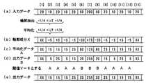
このような構成における具体的作用を、図4に基づいて説明する。図4(a)は、入力データを示したもので、それぞれの画素毎に図示のように0〜255の輝度信号のデータが与えられているものとする。これらの入力データは、輪郭抽出部12に入力されて、図4(b)に示すように、各画素に対応した輪郭成分Xが抽出される。この輪郭成分Xに輪郭補正処理部13でゲイン調整(この例では×1倍)したものと、遅延回路11で遅延してタイミングを合わせた入力データが、加算回路14で加算されて、図4(c)に示す出力データBを得る。この出力データBと入力データを比較すると、出力データBの方がより輪郭部分が強調されていることが分かる。
【0006】
また、画像信号の遠近感強調回路として、図示しないが、画像信号の1次微分信号と2次微分信号を用いて、物体の近景領域と遠景領域とを検出し、近景領域には輪郭強調処理を強く行い、遠景領域には輪郭強調を弱く行うことで、物体の遠近感を強調するためのものがある(例えば、特許文献1参照)。
【0007】
【特許文献1】
特開平10−126708号公報
【0008】
【発明が解決しようとする課題】
このように、図7に示す従来の方法は、輝度信号に、抽出した輪郭成分を加算している。しかし、輪郭成分の無い部分は、もとの輝度信号を用いているため、物体(人、建物等)と周囲の背景との差を視覚的に大きくするには、輪郭補正処理部13において、輪郭成分のゲインを強くする処理をする。ところが、ゲインを強くすることで、元々弱かった輪郭成分が強調されるのに対して、図4(c)に示すように、各画素の輝度信号の最大値は255で飽和してしまうため、輪郭成分の強い部分が頭打ちとなり、かえって物体と周囲の背景との差が現れにくくなるという問題があった。
また、特許文献1に記載の発明によれば、図7の回路の問題点は解決されるが、近景領域と遠景領域とで輪郭強調の強弱をつけるのみでは、必ずしも立体的に表現できないおそれがあった。
【0009】
本発明は、上記問題点に鑑みなされたもので、強い輪郭成分部分はより強調し、弱い輪郭成分や輪郭成分の無い部分は強調せず、入力信号を平均化することで、物体と周囲の背景との差を視覚的に大きくすることのできる立体的表現回路を提供することを目的とするものである。
【0010】
【課題を解決するための手段】
本発明は、入力ディジタル映像信号の輝度信号からなる入力データについて、着目画素とその近傍画素とから輪郭成分を抽出する輪郭抽出部と、この輪郭抽出部の出力と、この出力にタイミングを合わせた前記入力データとを加算して出力データBを演算する加算回路とからなる輪郭強調処理部を具備した立体的表現回路において、前記入力データの着目画素とその近傍画素とから平均化データAを演算する平均化回路と、前記輪郭抽出部の出力である輪郭成分と任意に設定された閾値とを比較する閾値処理部と、この閾値処理部の出力の大小に応じて前記平均化回路の平均化データAと前記輪郭強調処理部の出力データBとを選択的に出力するセレクタとからなることを特徴とする立体的表現回路である。
【0011】
このような構成とすることで、もともと輪郭成分の強い部分では輪郭強調したものを出力し、もともと輪郭成分の弱い部分では平均化データを出力するようになり、この結果、輪郭成分の強い部分と他の部分との差が明確になり、画像が立体的に見える。
【0012】
【発明の実施の形態】
本発明による立体的表現回路の構成を図1に基づいて説明する。以下、従来技術と同様の構成のものは同一符号を用いて説明する。
この図1において、データ入力端子10からの入力データは、平均化回路23と輪郭強調処理部39に入力される。この輪郭強調処理部39は、遅延回路11、輪郭抽出部12、輪郭補正処理部13、加算回路14から構成される。前記平均化回路23の出力は、遅延回路24を介してセレクタ27のA入力に入力される。輪郭強調処理部39の出力は、セレクタ27のB入力に入力される。また、前記輪郭強調処理部39における輪郭抽出部12の出力は、分岐して閾値処理部26に入力され、閾値設定信号入力端子25からの閾値設定信号も閾値処理部26に入力される。この閾値処理部26の出力は、セレクタ27のS入力に入力され、このS入力の信号に基づいて、前記遅延回路24からのA入力又は前記輪郭強調処理部からのB入力の何れか一方の入力信号を出力端子28に出力する。
【0013】
前記平均化回路23は、着目画素とこの着目画素の水平方向両隣に連続する3画素から平均化データAを演算するもので、具体的には、図2の回路を用いて行う。図2において、データ入力端子10からの入力データは、1/4係数回路31で1/4倍されて加算回路34に入力される。また、データ入力端子10からの入力データは、1D遅延回路29で1ドット遅延された後、1/2係数回路32に入力され、1/2倍されて、加算回路34に入力される。さらに、データ入力端子10からの入力データは、1D遅延回路29と1D遅延回路30で1ドットずつ計2ドット遅延された後、1/4係数回路33に入力され、1/4倍されて加算回路34に入力される。加算回路34では、これら3つのデータを加算し、この加算結果を平均化データAとして、データA出力端子35から出力する。この平均化データAが、セレクタ27のA入力に入力される。
【0014】
前記輪郭強調処理部39は、図7と同様、遅延回路11、輪郭抽出部12、輪郭補正処理部13、加算回路14から構成され、また、輪郭抽出部12は、図8と同様の構成であり、内部の3つの係数回路18、19、20の係数も、−1/4、1/2、−1/4を使用する。このような構成により、図3に示した入力データが輪郭抽出部12に入力されて、各画素に対応した図3(b)に示した輪郭成分Xが抽出される。この輪郭成分Xを輪郭補正処理部13でゲイン調整したものと、遅延回路11で遅延してタイミングを合わせた入力データが、加算回路14で加算されて、出力データBを得る。この出力データBが、セレクタ27のB入力に入力される。
【0015】
前記閾値処理部26は、前記輪郭強調処理部39における輪郭抽出部12の出力信号と閾値設定信号入力端子25からの閾値設定信号とを比較して、セレクタ27の選択信号を出力するものである。ここで、輪郭抽出部12の出力信号をX、閾値設定信号をYとすると、閾値処理部26では、|X|≦Yのときセレクタ27のA入力を選択する信号を出力し、|X|>Yのときセレクタ27のB入力を選択する信号を出力する。このような構成とすることで、閾値設定信号入力端子25で設定された値以下の輪郭成分は、平均化回路23で演算された平均化データAと置き換えられ、閾値設定信号入力端子25で設定された値以上の輪郭成分のみ入力データに反映されるようになる。
【0016】
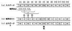
図3は、本発明回路を用いた場合の出力データの具体的な計算結果を示した図である。説明の都合上、画素番号を左から[1]〜[13]として説明する。
図3(a)は、各画素が輝度値で表された入力データを示したものとする。この図3(a)の入力データを輪郭抽出部12に入力すると、図3(b)の輪郭成分Xが演算によって求められる。例えば、着目画素[2]に対応した輪郭成分Xは、画素[1]の入力データに×−1/4倍したものと、画素[2]の入力データに×1/2倍したものと、画素[3]の入力データに×−1/4倍したものとの合計である。
同時に、図3(a)の入力データは、平均化回路23にも入力され、図3(c)の平均化データAが演算によって求められる。例えば、着目画素[2]に対応した平均化データAは、画素[1]の入力データに×1/4倍したものと、画素[2]の入力データに×1/2倍したものと、画素[3]の入力データに×1/4倍したものとの合計である。
さらに、図3(b)の輪郭成分Xと、図3(a)の入力データが加算回路14で加算されて、図3(d)の出力データBが求められる。
【0017】
上記の演算により求められた図3(c)の平均化データAと図3(d)の出力データBとがセレクタ27に入力される。このセレクタ27では、選択信号が閾値処理部26から入力され、それぞれの画素毎に、入力されたデータA、Bの何れか一方を出力する。閾値処理部26では、輪郭抽出部12で求められた図3(b)の輪郭成分Xの絶対値|X|を、閾値設定信号入力端子25からの閾値設定信号Y(図3の例では、Y=6)と比較して、|X|≦6となった画素では平均化データAを出力し、|X|>6となった画素では出力データBを出力する。図3(b)の輪郭成分Xを見てみると、画素[2]〜[5]、及び、画素[9]〜[12]の輪郭成分Xは、|X|=5であるため|X|≦6となり、これらの画素に対応した出力は、全て平均化データAを出力する。これに対して、画素[6]〜[8]の輪郭成分Xは、それぞれ|X|=30、75、30であるため|X|>6となり、これらの画素に対応した出力は、全て出力データBを出力する。このようにして、出力端子28から出力される図3(e)の出力データが決定される。
【0018】
ここで、図3(e)に示す本発明回路による出力データと、図4(c)に示す従来回路での出力データを比較すると、輪郭成分の弱い部分で差異が生じている。
図4(a)の入力データにおける画素[1]〜[5]部分の輝度値を見ると、最大の輝度差は10であるのに対し、図4(c)の従来回路の出力データにおける画素[2]〜[5]部分の輝度値は、最大の輝度差が20となっており、輪郭成分の弱い部分でも輪郭強調がされていることが分かる。この図4(c)の場合は、輪郭補正処理部13でのゲイン調整を×1倍としているが、このゲインを大きくすればするほど、もともと輪郭成分の弱い部分での輝度差が大きくなり、その結果、物体と周囲の背景との差が現れにくくなってしまう。
これに対し、図3(e)に示す本発明回路による出力データでは、画素[2]〜[5]部分の輪郭成分が小さいことを閾値処理部26で判別して、この部分では輪郭強調を行った出力の替わりに平均化データAを出力しているため、画素[2]〜[5]部分の最大の輝度差は10であり、入力データと変わらないことが分かる。また、閾値処理部26での判別は、輪郭補正処理部13でゲイン調整を行う前の輪郭成分Xを基準としているため、輪郭補正処理部13でゲインを大きく設定しても、もともと輪郭成分の強い部分のみにゲインを大きくした効果が現れ、もともと輪郭成分の弱い部分は平均化データAが出力されるようになり、その結果、物体と周囲の背景の差を視覚的に大きくすることができ、より立体的に見える。
【0019】
前記実施例では、セレクタ27によって、輪郭強調したデータであるか平均化したデータであるかを選択して何れか一方を出力するようにしたが、本発明はこれに限られるものではなく、図5に示すように、セレクタ27の替わりに混合器38を設けて、両者を混合して出力するようにしてもよい。
図5に示す回路は、基本的に図1に示した回路と同様の構成であるが、図1における閾値設定信号入力端子25の替わりに混合比設定指令信号入力端子36を設け、閾値処理部26の替わりに混合比選択処理部37を設け、セレクタ27の替わりに混合器38を設けたものである。混合比選択処理部37は、LUT(ルックアップテーブル)で構成され、輪郭抽出部12から入力される輪郭成分Xの絶対値|X|をアドレスとして、予めアドレス毎に設定された混合比Sを0〜1の範囲で出力する。このLUTに書き込まれた混合比Sは、混合比設定指令信号入力端子36からの混合比設定指令信号によって書き換えることができる。混合器38では、混合比選択処理部37からの混合比Sに基づいて、平均化データAと出力データBを混合して出力するが、その混合に用いる演算式は、
出力=A×S+B×(1−S) 但し、0≦S≦1
となる。
【0020】
上記演算式において、例えば、S=0.2である場合には、平均化データAが20%、出力データBが80%の割合で混合されて出力され、輪郭強調が強めに反映されるようになる。また、S=0.8の場合には、平均化データAが80%、出力データBが20%の割合で混合されて出力され、輪郭強調がわずかにしか反映されないようにすることができる。このように、輪郭強調の影響を調整できるので、LUTに書き込んでおく混合比Sの値は、輪郭成分Xの絶対値|X|が小さい場合には、混合比Sを1に近い値に設定することで、平均化データAの割合を大きくでき、輪郭成分Xの絶対値|X|が大きい場合には、混合比Sを0に近い値に設定することで、輪郭強調された出力データBの割合を大きくすることができる。このような構成にすることで、図1に示した閾値を用いる場合に比べてより細かい設定が可能となり、より立体的な表現を行うことができる。
【0021】
図5で示した前記実施例では、混合比選択処理部37で混合比Sを選択するアドレスとして、輪郭成分Xの絶対値|X|を使用したが、図6に示す回路のように、データ入力端子10からの入力データの輝度値を直接アドレスとして用いて混合比Sを選択するようにしてもよい。
【0022】
前記実施例では、輪郭抽出部12の3つの係数回路は、−1/4係数回路18、1/2係数回路19、−1/4係数回路20で構成したが、これに限られるものではなく、これとは異なる係数の組合せを用いてもよい。但し、係数の合計が0になるように選ぶことが望ましく、例えば、−1/5、2/5、−1/5というように設定してもよい。
【0023】
前記実施例では、平均化回路23の3つの係数回路は、1/4係数回路31、1/2係数回路32、1/4係数回路33で構成したが、これに限られるものではなく、これとは異なる係数の組合せを用いてもよい。但し、係数の合計が1になるように選ぶことが望ましく、例えば、1/5、3/5、1/5というように設定してもよい。
また、平均化回路23を無くして、平均化データの替わりに入力データをそのままセレクタ27又は混合器38のA入力に入力するようにしてもよい。このような構成にしても、もともと輪郭成分の弱い部分に対する輪郭強調を防ぐことはできるので、物体と周囲の背景の差を視覚的に大きくすることは可能である。
【0024】
【発明の効果】
請求項1記載の発明によれば、もともと輪郭成分の強い部分では輪郭強調したものを出力し、もともと輪郭成分の弱い部分では入力データをそのまま出力するようにしたので、この結果、輪郭成分の強い部分と他の部分との差が明確になり、画像が立体的に見える。
【0025】
請求項2記載の発明によれば、もともと輪郭成分の強い部分では輪郭強調したものを出力し、もともと輪郭成分の弱い部分では平均化データを出力するようにしたので、この結果、輪郭成分の強い部分と他の部分との差が明確になり、画像が立体的に見える。
【0026】
請求項3記載の発明によれば、輪郭成分をアドレスとして0〜1の値を持つ混合比Sを混合比選択処理部で選択して[入力データ]×S+[出力データB]×(1−S)を演算して出力するようにしたので、例えば、もともと輪郭成分の弱い部分では、混合比Sを1に近い値に設定することで入力データの割合を大きくでき、もともと輪郭成分の弱い部分では、混合比Sを0に近い値に設定することで輪郭強調された出力データBの割合を大きくすることができるようになり、輪郭成分の値によって任意の混合が行え、この結果、輪郭成分の強い部分と他の部分との差が明確になり、画像が立体的に見える。
【0027】
請求項4記載の発明によれば、輪郭成分をアドレスとして0〜1の値を持つ混合比Sを混合比選択処理部で選択して[平均化データA]×S+[出力データB]×(1−S)を演算して出力するようにしたので、例えば、もともと輪郭成分の弱い部分では、混合比Sを1に近い値に設定することで平均化データAの割合を大きくでき、もともと輪郭成分の弱い部分では、混合比Sを0に近い値に設定することで輪郭強調された出力データBの割合を大きくすることができるようになり、輪郭成分の値によって任意の混合が行え、この結果、輪郭成分の強い部分と他の部分との差が明確になり、画像が立体的に見える。
【0028】
請求項5記載の発明によれば、入力データをアドレスとして0〜1の値を持つ混合比Sを混合比選択処理部で選択して[入力データ]×S+[出力データB]×(1−S)を演算して出力するようにしたので、入力データの値によって任意の混合が行え、この結果、輪郭成分の強い部分と他の部分との差が明確になり、画像が立体的に見える。
【0029】
請求項6記載の発明によれば、入力データをアドレスとして0〜1の値を持つ混合比Sを混合比選択処理部で選択して[平均化データA]×S+[出力データB]×(1−S)を演算して出力するようにしたので、入力データの値によって任意の混合が行え、この結果、輪郭成分の強い部分と他の部分との差が明確になり、画像が立体的に見える。
【0030】
請求項7記載の発明によれば、平均化回路は、入力デ−タを1/4倍して出力する第一の1/4係数回路と、入力デ−タを1D遅延回路によって1ドット遅らせたものを1/2倍して出力する1/2係数回路と、入力デ−タを1D遅延回路2つによって2ドット遅らせたものを1/4倍して出力する第二の1/4係数回路と、これら3つの係数回路の出力を加算して出力する加算回路とからなるようにしたので、水平方向に連続する3画素から平均化データAを得ることができる。
【0031】
請求項8記載の発明によれば、輪郭抽出部は、入力デ−タを−1/4倍して出力する第一の1/4係数回路と、入力デ−タを1D遅延回路によって1ドット遅らせたものを1/2倍して出力する1/2係数回路と、入力デ−タを1D遅延回路2つによって2ドット遅らせたものをー1/4倍して出力する第二の1/4係数回路と、これら3つの係数回路の出力を加算して出力する加算回路とからなるようにしたので、水平方向に連続する3画素から輪郭成分を得ることができる。
【図面の簡単な説明】
【図1】本発明による立体的表現回路の構成を示したブロック図である。
【図2】図1における平均化回路23の構成を示したブロック図である。
【図3】本発明の立体的表現回路に(a)入力データが入力された場合の各部の計算結果を示した図で、(b)は輪郭成分X、(c)は平均化データA、(d)は出力データB、(e)は出力データを示している。
【図4】従来の立体的表現回路に(a)入力データが入力された場合の各部の計算結果を示した図で、(b)は輪郭成分X、(c)は出力データBを示している。
【図5】本発明の他の実施例を示したブロック図で、図1の回路のセレクタ27を混合器38に替え、閾値処理部26を混合比選択処理部37に替えたものである。
【図6】本発明の他の実施例を示したブロック図で、図5の回路において混合比選択処理部37に入力される信号を、輪郭成分Xから入力データに替えたものである。
【図7】従来の立体的表現回路の構成を示したブロック図である。
【図8】図7における輪郭抽出部12の構成を示したブロック図である。
【符号の説明】
10…データ入力端子、11…遅延回路、12…輪郭抽出部、13…輪郭補正処理部、14…加算回路、15…データB出力端子、16…1D遅延回路、17…1D遅延回路、18…−1/4係数回路、19…1/2係数回路、20…−1/4係数回路、21…加算回路、22…輪郭成分出力端子、23…平均化回路、24…遅延回路、25…閾値設定信号入力端子、26…閾値処理部、27…セレクタ、28…出力端子、29…1D遅延回路、30…1D遅延回路、31…1/4係数回路、32…1/2係数回路、33…1/4係数回路、34…加算回路、35…データA出力端子、36…混合比決定指令信号入力端子、37…混合比選択処理部、38…混合器、39…輪郭強調処理部。[0001]
TECHNICAL FIELD OF THE INVENTION
The present invention relates to a three-dimensional expression circuit using contour enhancement processing in digital image processing.
[Prior art]
2. Description of the Related Art Conventionally, there is a technique for performing an outline emphasis process on an image displayed on a display device such as a PDP (plasma display panel) and expressing the display image in three dimensions. This is based on the fact that there is a strong appearance of contour components between objects such as people and buildings and the surrounding background. Appears, and the human eye feels that the image is three-dimensional.
[0003]
FIG. 7 shows a conventional three-dimensional expression circuit. In FIG. 7, input data from a
[0004]
The
[0005]
A specific operation in such a configuration will be described with reference to FIG. FIG. 4A shows input data, and it is assumed that data of a luminance signal of 0 to 255 is given to each pixel as shown in FIG. These input data are input to the
[0006]
As a perspective emphasis circuit for the image signal, although not shown, the first and second differential signals of the image signal are used to detect the near and distant areas of the object, and the near area is subjected to contour enhancement processing. Is performed strongly, and in the distant view area, contour enhancement is performed weakly to enhance the perspective of the object (for example, see Patent Document 1).
[0007]
[Patent Document 1]
JP 10-126708 A
[Problems to be solved by the invention]
As described above, the conventional method shown in FIG. 7 adds the extracted contour component to the luminance signal. However, since a portion having no contour component uses the original luminance signal, in order to visually increase the difference between the object (person, building, etc.) and the surrounding background, the contour
Further, according to the invention described in
[0009]
The present invention has been made in view of the above problems, and emphasizes a strong contour component portion, does not emphasize a weak contour component or a portion without a contour component, and averages an input signal, thereby averaging an object and surroundings. It is an object of the present invention to provide a three-dimensional expression circuit capable of visually increasing a difference from a background.
[0010]
[Means for Solving the Problems]
According to the present invention, for input data consisting of a luminance signal of an input digital video signal, a contour extracting unit that extracts a contour component from a pixel of interest and its neighboring pixels, an output of the contour extracting unit, and a timing synchronized with this output In a three-dimensional expression circuit provided with a contour emphasis processing unit comprising an addition circuit for adding the input data and calculating an output data B, an averaged data A is calculated from a pixel of interest of the input data and neighboring pixels. Averaging circuit, a threshold processing unit that compares a contour component output from the contour extraction unit with an arbitrarily set threshold, and averaging the averaging circuit according to the magnitude of the output of the threshold processing unit. A three-dimensional expression circuit comprising a selector for selectively outputting data A and output data B of the contour emphasis processing section.
[0011]
By adopting such a configuration, an edge-enhanced portion is output in a portion where the contour component is originally strong, and an averaged data is output in a portion where the contour component is originally weak. The difference from other parts becomes clear, and the image looks three-dimensional.
[0012]
BEST MODE FOR CARRYING OUT THE INVENTION
The configuration of the three-dimensional expression circuit according to the present invention will be described with reference to FIG. Hereinafter, components having the same configuration as the related art will be described using the same reference numerals.
In FIG. 1, input data from a
[0013]
The
[0014]
The outline
[0015]
The
[0016]
FIG. 3 is a diagram showing a specific calculation result of output data when the circuit of the present invention is used. For convenience of explanation, pixel numbers are described as [1] to [13] from the left.
FIG. 3A shows input data in which each pixel is represented by a luminance value. When the input data of FIG. 3A is input to the
At the same time, the input data of FIG. 3A is also input to the averaging
Further, the contour component X of FIG. 3B and the input data of FIG. 3A are added by the
[0017]
The averaged data A in FIG. 3C and the output data B in FIG. 3D obtained by the above calculation are input to the
[0018]
Here, when the output data of the circuit of the present invention shown in FIG. 3 (e) is compared with the output data of the conventional circuit shown in FIG. 4 (c), a difference occurs in a portion having a weak outline component.
Looking at the luminance values of the pixels [1] to [5] in the input data in FIG. 4A, the maximum luminance difference is 10, whereas the pixel in the output data of the conventional circuit in FIG. The luminance values of the parts [2] to [5] have a maximum luminance difference of 20, which indicates that the outline is emphasized even in a part having a weak outline component. In the case of FIG. 4 (c), the gain adjustment in the contour
On the other hand, in the output data of the circuit of the present invention shown in FIG. 3E, the
[0019]
In the above-described embodiment, the
The circuit shown in FIG. 5 has basically the same configuration as the circuit shown in FIG. 1, except that a mixing ratio setting command
Output = A × S + B × (1-S) where 0 ≦ S ≦ 1
It becomes.
[0020]
In the above equation, for example, when S = 0.2, the averaged data A is mixed and output at a ratio of 20% and the output data B is output at a ratio of 80%, so that the outline emphasis is strongly reflected. become. When S = 0.8, the averaged data A and the output data B are mixed and output at a ratio of 80% and 20%, respectively, so that the edge enhancement is slightly reflected. As described above, since the influence of contour enhancement can be adjusted, the value of the mixture ratio S written in the LUT is set to a value close to 1 when the absolute value | X | of the contour component X is small. In this case, the ratio of the averaged data A can be increased, and when the absolute value | X | of the contour component X is large, the mixture ratio S is set to a value close to 0, so that the contour-enhanced output data B Can be increased. With such a configuration, it is possible to perform more detailed settings than in the case of using the threshold shown in FIG. 1, and it is possible to perform a more three-dimensional expression.
[0021]
In the embodiment shown in FIG. 5, the absolute value | X | of the contour component X is used as an address for selecting the mixture ratio S in the mixture ratio
[0022]
In the above embodiment, the three coefficient circuits of the
[0023]
In the above embodiment, the three coefficient circuits of the averaging
Further, the averaging
[0024]
【The invention's effect】
According to the first aspect of the present invention, an edge-enhanced portion is output in a portion where the contour component is originally strong, and the input data is output as it is in a portion where the contour component is originally weak. The difference between the part and the other part becomes clear, and the image looks three-dimensional.
[0025]
According to the second aspect of the present invention, an edge-enhanced portion is output at a portion where the contour component is originally strong, and averaged data is output at a portion where the contour component is originally weak. The difference between the part and the other part becomes clear, and the image looks three-dimensional.
[0026]
According to the third aspect of the present invention, a mixture ratio S having a value of 0 to 1 is selected by the mixture ratio selection processing unit using the contour component as an address, and [input data] × S + [output data B] × (1- S) is calculated and output. For example, in a portion where the contour component is originally weak, the ratio of the input data can be increased by setting the mixture ratio S to a value close to 1, and a portion where the contour component is originally weak can be obtained. By setting the mixture ratio S to a value close to 0, it is possible to increase the ratio of the output data B that has been edge-emphasized, and to perform arbitrary mixing depending on the value of the contour component. The difference between the strong part and other parts becomes clear, and the image looks three-dimensional.
[0027]
According to the fourth aspect of the invention, a mixture ratio S having a value of 0 to 1 is selected by the mixture ratio selection processing unit using the contour component as an address, and [averaged data A] × S + [output data B] × ( 1-S) is calculated and output. For example, in a portion where the contour component is originally weak, the ratio of the averaged data A can be increased by setting the mixture ratio S to a value close to 1, and the contour In the weak part of the component, by setting the mixture ratio S to a value close to 0, it becomes possible to increase the ratio of the output data B with the edge emphasized, and arbitrary mixing can be performed by the value of the outline component. As a result, the difference between a portion having a strong contour component and other portions becomes clear, and the image looks three-dimensional.
[0028]
According to the fifth aspect of the invention, the input data is used as an address to select a mixing ratio S having a value of 0 to 1 in the mixing ratio selection processing unit, and [input data] × S + [output data B] × (1- Since S) is calculated and output, arbitrary mixing can be performed depending on the value of the input data. As a result, the difference between the portion having a strong contour component and the other portion becomes clear, and the image looks three-dimensional. .
[0029]
According to the sixth aspect of the present invention, the mixture ratio S having a value of 0 to 1 is selected by the mixture ratio selection processing unit using the input data as an address, and [averaged data A] × S + [output data B] × ( Since 1-S) is calculated and output, arbitrary mixing can be performed depending on the value of the input data. As a result, the difference between a portion having a strong contour component and another portion becomes clear, and the image becomes three-dimensional. Looks like.
[0030]
According to the seventh aspect of the present invention, the averaging circuit delays the input data by one dot by the 1D delay circuit, and the first quarter coefficient circuit which outputs the input data by 1/4. And a second 1/4 coefficient which outputs the input data delayed by 2 dots by two 1D delay circuits by 1/4 times and outputs the result. Since the circuit includes a circuit and an addition circuit that adds and outputs the outputs of the three coefficient circuits, the averaged data A can be obtained from three pixels that are continuous in the horizontal direction.
[0031]
According to the eighth aspect of the present invention, the contour extracting section outputs the input data by one dot by the 1/4 coefficient circuit for outputting the input data by -1/4 and the 1D delay circuit. A 1/2 coefficient circuit that outputs the delayed data by 1/2, and a second 1/2 that outputs the input data delayed by 2 dots by two 1D delay circuits by 1/4. Since the circuit includes the four coefficient circuits and the addition circuit that adds and outputs the outputs of the three coefficient circuits, a contour component can be obtained from three pixels that are continuous in the horizontal direction.
[Brief description of the drawings]
FIG. 1 is a block diagram showing a configuration of a three-dimensional expression circuit according to the present invention.
FIG. 2 is a block diagram showing a configuration of an averaging
FIGS. 3A and 3B are diagrams showing calculation results of each unit when input data is input to the three-dimensional expression circuit of the present invention, wherein FIG. 3B shows a contour component X, FIG. (D) shows the output data B, and (e) shows the output data.
4A and 4B are diagrams showing calculation results of respective units when input data is input to a conventional three-dimensional expression circuit, where FIG. 4B shows a contour component X and FIG. 4C shows output data B; I have.
5 is a block diagram showing another embodiment of the present invention, in which the
6 is a block diagram showing another embodiment of the present invention, in which a signal input to the mixture ratio
FIG. 7 is a block diagram showing a configuration of a conventional three-dimensional expression circuit.
8 is a block diagram showing a configuration of a
[Explanation of symbols]
DESCRIPTION OF
Claims (8)
Translated fromJapanese[入力データ]×S+[出力データB]×(1−S)
を演算して出力とする混合器とからなることを特徴とする立体的表現回路。For input data consisting of a luminance signal of an input digital video signal, a contour extraction unit for extracting a contour component from a pixel of interest and neighboring pixels, an output of the contour extraction unit, and the input data synchronized with the output. In the three-dimensional expression circuit having an outline emphasis processing unit consisting of an addition circuit for calculating output data B by adding And a mixing ratio selection processing unit that outputs the calculated mixing ratio S.
[Input data] × S + [Output data B] × (1-S)
A three-dimensional expression circuit comprising:
[平均化データA]×S+[出力データB]×(1−S)
を演算して出力とする混合器とからなることを特徴とする立体的表現回路。For input data consisting of a luminance signal of an input digital video signal, a contour extraction unit for extracting a contour component from a pixel of interest and neighboring pixels, an output of the contour extraction unit, and the input data synchronized with the output. Averaging circuit for calculating averaged data A from a pixel of interest of the input data and its neighboring pixels in a three-dimensional expression circuit having an outline emphasis processing unit comprising an addition circuit for calculating output data B by adding And a mixture ratio selection processing unit that outputs a mixture ratio S arbitrarily set within a range of 0 to 1 according to the magnitude of the output of the contour extraction unit.
[Averaged data A] × S + [Output data B] × (1-S)
A three-dimensional expression circuit comprising:
[入力データ]×S+[出力データB]×(1−S)
を演算して出力とする混合器とからなることを特徴とする立体的表現回路。For input data consisting of a luminance signal of an input digital video signal, a contour extraction unit for extracting a contour component from a pixel of interest and neighboring pixels, an output of the contour extraction unit, and the input data synchronized with the output. And a summing circuit for calculating output data B by adding the input data to the input data, wherein a mixing ratio arbitrarily set within a range of 0 to 1 according to the magnitude of the input data. Using a mixture ratio selection processing section that outputs S, and the mixture ratio S,
[Input data] × S + [Output data B] × (1-S)
A three-dimensional expression circuit comprising:
[平均化データA]×S+[出力データB]×(1−S)
を演算して出力とする混合器とからなることを特徴とする立体的表現回路。For input data consisting of a luminance signal of an input digital video signal, a contour extraction unit for extracting a contour component from a pixel of interest and neighboring pixels, an output of the contour extraction unit, and the input data synchronized with the output. Averaging circuit for calculating averaged data A from a pixel of interest of the input data and its neighboring pixels in a three-dimensional expression circuit having an outline emphasis processing unit comprising an addition circuit for calculating output data B by adding And a mixing ratio selection processing unit that outputs a mixing ratio S arbitrarily set within a range of 0 to 1 according to the magnitude of the input data.
[Averaged data A] × S + [Output data B] × (1-S)
A three-dimensional expression circuit comprising:
Priority Applications (1)
| Application Number | Priority Date | Filing Date | Title |
|---|---|---|---|
| JP2002323603AJP2004159148A (en) | 2002-11-07 | 2002-11-07 | Circuit for three-dimensional representation |
Applications Claiming Priority (1)
| Application Number | Priority Date | Filing Date | Title |
|---|---|---|---|
| JP2002323603AJP2004159148A (en) | 2002-11-07 | 2002-11-07 | Circuit for three-dimensional representation |
Publications (1)
| Publication Number | Publication Date |
|---|---|
| JP2004159148Atrue JP2004159148A (en) | 2004-06-03 |
Family
ID=32803428
Family Applications (1)
| Application Number | Title | Priority Date | Filing Date |
|---|---|---|---|
| JP2002323603APendingJP2004159148A (en) | 2002-11-07 | 2002-11-07 | Circuit for three-dimensional representation |
Country Status (1)
| Country | Link |
|---|---|
| JP (1) | JP2004159148A (en) |
Cited By (14)
| Publication number | Priority date | Publication date | Assignee | Title |
|---|---|---|---|---|
| JP2007318313A (en)* | 2006-05-24 | 2007-12-06 | Toshiba Corp | Video signal processing apparatus and video signal processing method |
| JP2007324764A (en)* | 2006-05-30 | 2007-12-13 | Toshiba Corp | Video signal processing apparatus and video signal processing method |
| JP2008033897A (en)* | 2006-06-29 | 2008-02-14 | Matsushita Electric Ind Co Ltd | Image processing apparatus, image processing method, program, recording medium, and integrated circuit |
| JP2009038794A (en)* | 2007-07-06 | 2009-02-19 | Panasonic Corp | Image processing apparatus, image processing method, image processing system, program, recording medium, and integrated circuit |
| JP2010515896A (en)* | 2007-01-10 | 2010-05-13 | トムトム インターナショナル ベスローテン フエンノートシャップ | Navigation apparatus and method for improved map display |
| US20110001991A1 (en)* | 2009-07-01 | 2011-01-06 | Canon Kabushiki Kaisha | Image processing device and image processing apparatus |
| US7869649B2 (en) | 2006-05-08 | 2011-01-11 | Panasonic Corporation | Image processing device, image processing method, program, storage medium and integrated circuit |
| US8009903B2 (en) | 2006-06-29 | 2011-08-30 | Panasonic Corporation | Image processor, image processing method, storage medium, and integrated circuit that can adjust a degree of depth feeling of a displayed high-quality image |
| US8131098B2 (en) | 2007-07-06 | 2012-03-06 | Panasonic Corporation | Image processing device, image processing method, image processing system, program, storage medium, and integrated circuit |
| US8134646B2 (en) | 2006-05-24 | 2012-03-13 | Kabushiki Kaisha Toshiba | Video signal processing device and video signal processing method |
| US8265385B2 (en) | 2008-11-12 | 2012-09-11 | Samsung Electronics Co., Ltd. | Image processing apparatus and method of enhancing depth perception |
| US8692911B2 (en) | 2012-01-31 | 2014-04-08 | Kabushiki Kaisha Toshiba | Image processing device, image processing method, and camera module |
| US9013750B2 (en) | 2009-06-25 | 2015-04-21 | Canon Kabushiki Kaisha | Image processing for processing image data in correspondence with each pixel of an image |
| US9635218B2 (en) | 2009-07-03 | 2017-04-25 | Canon Kabushiki Kaisha | Image processing based on a pixel value in image data |
- 2002
- 2002-11-07JPJP2002323603Apatent/JP2004159148A/enactivePending
Cited By (20)
| Publication number | Priority date | Publication date | Assignee | Title |
|---|---|---|---|---|
| US7869649B2 (en) | 2006-05-08 | 2011-01-11 | Panasonic Corporation | Image processing device, image processing method, program, storage medium and integrated circuit |
| JP2007318313A (en)* | 2006-05-24 | 2007-12-06 | Toshiba Corp | Video signal processing apparatus and video signal processing method |
| US8134646B2 (en) | 2006-05-24 | 2012-03-13 | Kabushiki Kaisha Toshiba | Video signal processing device and video signal processing method |
| JP2007324764A (en)* | 2006-05-30 | 2007-12-13 | Toshiba Corp | Video signal processing apparatus and video signal processing method |
| JP2008033897A (en)* | 2006-06-29 | 2008-02-14 | Matsushita Electric Ind Co Ltd | Image processing apparatus, image processing method, program, recording medium, and integrated circuit |
| US8009903B2 (en) | 2006-06-29 | 2011-08-30 | Panasonic Corporation | Image processor, image processing method, storage medium, and integrated circuit that can adjust a degree of depth feeling of a displayed high-quality image |
| JP2010515896A (en)* | 2007-01-10 | 2010-05-13 | トムトム インターナショナル ベスローテン フエンノートシャップ | Navigation apparatus and method for improved map display |
| JP2009038794A (en)* | 2007-07-06 | 2009-02-19 | Panasonic Corp | Image processing apparatus, image processing method, image processing system, program, recording medium, and integrated circuit |
| US8131098B2 (en) | 2007-07-06 | 2012-03-06 | Panasonic Corporation | Image processing device, image processing method, image processing system, program, storage medium, and integrated circuit |
| US8265385B2 (en) | 2008-11-12 | 2012-09-11 | Samsung Electronics Co., Ltd. | Image processing apparatus and method of enhancing depth perception |
| US9013750B2 (en) | 2009-06-25 | 2015-04-21 | Canon Kabushiki Kaisha | Image processing for processing image data in correspondence with each pixel of an image |
| US20110001991A1 (en)* | 2009-07-01 | 2011-01-06 | Canon Kabushiki Kaisha | Image processing device and image processing apparatus |
| US8976411B2 (en)* | 2009-07-01 | 2015-03-10 | Canon Kabushiki Kaisha | Image processing in correspondence with each pixel of an image |
| JP2011030216A (en)* | 2009-07-01 | 2011-02-10 | Canon Inc | Image processing device and image processing apparatus |
| US9466017B2 (en) | 2009-07-01 | 2016-10-11 | Canon Kabushiki Kaisha | Image processing device and image processing apparatus which process image data in correspondence with one or more image pixels of an image |
| US9661182B2 (en) | 2009-07-01 | 2017-05-23 | Canon Kabushiki Kaisha | Image processing device and image processing apparatus |
| US9888150B2 (en) | 2009-07-01 | 2018-02-06 | Canon Kabushiki Kaisha | Image processing apparatus, and image processing device which processes image data in correspondence with one or more pixels of an image |
| US9635218B2 (en) | 2009-07-03 | 2017-04-25 | Canon Kabushiki Kaisha | Image processing based on a pixel value in image data |
| US10063748B2 (en) | 2009-07-03 | 2018-08-28 | Canon Kabushiki Kaisha | Image processing apparatus having a determination unit that determines an attribute value which specifies processing content of one or more pixels |
| US8692911B2 (en) | 2012-01-31 | 2014-04-08 | Kabushiki Kaisha Toshiba | Image processing device, image processing method, and camera module |
Similar Documents
| Publication | Publication Date | Title |
|---|---|---|
| JP2004159148A (en) | Circuit for three-dimensional representation | |
| JP5094219B2 (en) | Image processing apparatus, image processing method, program, recording medium, and integrated circuit | |
| JP4746575B2 (en) | Image processing apparatus and method | |
| KR100532121B1 (en) | Method and apparatus for image detail enhancement | |
| CN100530245C (en) | Device and its method for producing three dimension image from two dimension image | |
| JP2013050962A (en) | Image processing apparatus, image processing method, image processing program, and integrated circuit | |
| JP2008017458A (en) | Image processing apparatus, image processing method, image processing program, and integrated circuit | |
| JP2002344746A (en) | Circuit and method for contour correction | |
| JP2008176447A (en) | Image processor, image processing method, program of image processing method, and recording medium which records program of image processing method | |
| US9386291B2 (en) | Video signal processing device | |
| JP2010028178A (en) | Image quality improving device and method | |
| JP2001128031A (en) | Edge enhancement method and circuit | |
| JP2008021163A (en) | Image processing device | |
| CN105830438A (en) | Image display device | |
| TW200931947A (en) | Image processing apparatus and image processing method | |
| JP4381240B2 (en) | Image processing apparatus, image display apparatus using the same, image processing method, and program for causing computer to execute the same | |
| JP4419441B2 (en) | Image processing apparatus, image processing method, and program | |
| JP5615043B2 (en) | Image processing apparatus and image processing method | |
| JP2003348379A (en) | Image display device and image processing apparatus, and image processing method | |
| CN1061201C (en) | Horizontal profile increasing signal processing circuit | |
| Lin et al. | An adaptive color transient improvement algorithm | |
| JPH11289476A (en) | Edge enhancement circuit | |
| JP2000244775A (en) | Contour emphasis device | |
| JP2001285672A (en) | Contour correction device | |
| JP3743055B2 (en) | Image contour enhancement method and apparatus |
Legal Events
| Date | Code | Title | Description |
|---|---|---|---|
| A621 | Written request for application examination | Free format text:JAPANESE INTERMEDIATE CODE: A621 Effective date:20051031 | |
| A977 | Report on retrieval | Free format text:JAPANESE INTERMEDIATE CODE: A971007 Effective date:20080130 | |
| A131 | Notification of reasons for refusal | Free format text:JAPANESE INTERMEDIATE CODE: A131 Effective date:20080226 | |
| A711 | Notification of change in applicant | Free format text:JAPANESE INTERMEDIATE CODE: A711 Effective date:20080515 | |
| A521 | Request for written amendment filed | Free format text:JAPANESE INTERMEDIATE CODE: A523 Effective date:20080620 | |
| A02 | Decision of refusal | Free format text:JAPANESE INTERMEDIATE CODE: A02 Effective date:20080805 |