JP2004157288A - Display device - Google Patents
Display deviceDownload PDFInfo
- Publication number
- JP2004157288A JP2004157288AJP2002322229AJP2002322229AJP2004157288AJP 2004157288 AJP2004157288 AJP 2004157288AJP 2002322229 AJP2002322229 AJP 2002322229AJP 2002322229 AJP2002322229 AJP 2002322229AJP 2004157288 AJP2004157288 AJP 2004157288A
- Authority
- JP
- Japan
- Prior art keywords
- display
- gradation
- reference potential
- display device
- output terminal
- Prior art date
- Legal status (The legal status is an assumption and is not a legal conclusion. Google has not performed a legal analysis and makes no representation as to the accuracy of the status listed.)
- Pending
Links
Images


Classifications
- G—PHYSICS
- G02—OPTICS
- G02F—OPTICAL DEVICES OR ARRANGEMENTS FOR THE CONTROL OF LIGHT BY MODIFICATION OF THE OPTICAL PROPERTIES OF THE MEDIA OF THE ELEMENTS INVOLVED THEREIN; NON-LINEAR OPTICS; FREQUENCY-CHANGING OF LIGHT; OPTICAL LOGIC ELEMENTS; OPTICAL ANALOGUE/DIGITAL CONVERTERS
- G02F1/00—Devices or arrangements for the control of the intensity, colour, phase, polarisation or direction of light arriving from an independent light source, e.g. switching, gating or modulating; Non-linear optics
- G02F1/01—Devices or arrangements for the control of the intensity, colour, phase, polarisation or direction of light arriving from an independent light source, e.g. switching, gating or modulating; Non-linear optics for the control of the intensity, phase, polarisation or colour
- G02F1/13—Devices or arrangements for the control of the intensity, colour, phase, polarisation or direction of light arriving from an independent light source, e.g. switching, gating or modulating; Non-linear optics for the control of the intensity, phase, polarisation or colour based on liquid crystals, e.g. single liquid crystal display cells
- G—PHYSICS
- G03—PHOTOGRAPHY; CINEMATOGRAPHY; ANALOGOUS TECHNIQUES USING WAVES OTHER THAN OPTICAL WAVES; ELECTROGRAPHY; HOLOGRAPHY
- G03B—APPARATUS OR ARRANGEMENTS FOR TAKING PHOTOGRAPHS OR FOR PROJECTING OR VIEWING THEM; APPARATUS OR ARRANGEMENTS EMPLOYING ANALOGOUS TECHNIQUES USING WAVES OTHER THAN OPTICAL WAVES; ACCESSORIES THEREFOR
- G03B21/00—Projectors or projection-type viewers; Accessories therefor
- G03B21/54—Accessories
- G03B21/56—Projection screens
Landscapes
- Physics & Mathematics (AREA)
- General Physics & Mathematics (AREA)
- Nonlinear Science (AREA)
- Chemical & Material Sciences (AREA)
- Crystallography & Structural Chemistry (AREA)
- Optics & Photonics (AREA)
- Control Of Indicators Other Than Cathode Ray Tubes (AREA)
- Liquid Crystal Display Device Control (AREA)
- Liquid Crystal (AREA)
- Transforming Electric Information Into Light Information (AREA)
Abstract
Translated fromJapaneseDescription
Translated fromJapanese【0001】
【発明の属する技術分野】
本発明は、反射表示と透過表示との両方の表示を行うとともに、印加電圧と透過率又は印加電圧と反射率との関係が反射表示と透過表示との表示モードで異なる半透過方式の液晶表示装置等の表示装置に関するものである。
【0002】
【従来の技術】
液晶表示装置をはじめとする表示装置では、一般に、階調特性は、入力階調信号に対して出力輝度が線形であることが良いとされる。ここで、入力階調信号値対出力輝度の特性をγ特性という。このγ特性とは、具体的には、表示装置の輝度Lが表示装置への入力階調信号値Eのγ乗に比例して変化することをいう。これを式で表すと、L=KEγ(一般にγ=2.2〜3、Kは定数)である。
【0003】
このように、表示装置は、入力階調信号に対する出力輝度が線形ではなく、上記γ特性の関係を持つものが多いため、そのままでは正しい階調表示ができない。
【0004】
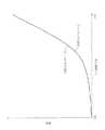
そこで、表示装置では、図7において「一般的な画像のγ逆特性」として示すように、正しい階調表現を行うためには、このことを考慮して予め入力階調信号値Eの1/γ乗を用いて補正をかける必要がある。これをγ補正という。これにより、同図において、「正しい階調特性」として示すように、L=KE(Kは定数)となる入力階調信号に対して出力輝度が線形となる関係が得られる。
【0005】
ところで、γ逆特性に対応するγ特性を得るためには、図8に示すように、表示装置のγ補正回路を用いる。このγ補正回路では、64階調を実現するために、64段階に区切った64個の出力端子からいずれかの出力端子を各セレクタにて選ぶことによって、最適な64階調を実現する。これにより、正しい階調表示ができるようになる。なお、上記γ補正回路は、図9に示すように、液晶表示装置70のソースドライバ71に内蔵されている。
【0006】
上記従来の液晶表示装置では、γ補正の最適値を一度設定すると、液晶表示装置の動作中の変更は不可能であるものの、表示モードが不変の場合においては問題なかった。
【0007】
しかしながら、近年では、明るい場所では低消費電力化のため、バックライトをOFFして外部光を用いる反射方式(仮に「モード1」と呼ぶ)と、暗い場所では従来のようにバックライトによる透過方式(仮に「モード2」と呼ぶ)の両方の利点を合わせた半透過方式の液晶表示装置が市販されている。
【0008】
上記半透過方式の液晶表示装置においては、透過型から反射型に切り替えると、図10に示すように、階調−輝度特性が完全に一致しないため、同じ画像でも見え方が違ってしまう。この理由は、図11に示すように、透過時と反射時との差によって、印加電圧(V)−透過率(T)特性が一致していないためである。なお、同図においては、印加電圧(V)−透過率(T)の特性について説明しているが、印加電圧(V)−反射率との関係においても同様のことが言える。
【0009】
また、それぞれの表示モードで階調表示を変えたいというニーズも考えられる。つまり、1つの階調設定ではユーザに違和感を与えてしまう。
【0010】
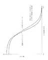
そこで、図12に示すように、ソースドライバの階調−電圧印加特性の特性カーブを複数用意しておき、それぞれの表示モードを切り替えるときに連動して切り替えるようにする。なお、同図では設定は2つとしているが、勿論、2つ以上の設定がありその中から選べるようにしてもよい。これによって、図13に示すように、階調−輝度特性を透過時と反射時で完全に一致させることができる。
【0011】
表示モードによって階調レベルの変更が可能な従来の表示装置として、例えば特許文献1では、図14に示すように、2種類の基準電位発生回路81・82を用意しておき、これら基準電位発生回路81・82のいずれかを反射/透過判定信号にて選択することにより、「透過」及び「反射」の階調毎の透過率/反射率を合わせている。
【0012】
また、例えば特許文献2や特許文献3では、従来、γ補正回路の基準電圧を作る回路が抵抗分圧比で決定される構成となっており、使用モードに合わせてγ補正係数を変えることができなかったという問題に鑑み、図15に示すように、γ補正回路90の基準電圧に係る情報をメモリ91に蓄積しておき、それを取り出してD/A変換して基準電圧V1〜V10を作るようにしている。これにより、簡単に任意のγ補正係数を得ることができるとしている。
【0013】
【特許文献1】
特開2000−193936号公報(平成12年7月14日公開)
【0014】
【特許文献2】
特開平10−333648号公報(1998年12月18日公開)
【0015】
【特許文献3】
特開昭63−38989号公報(1988年2月19日公開)
【0016】
【発明が解決しようとする課題】
しかしながら、上記従来の表示装置のうち、特許文献1では、各表示モードにおいては再設定が不可能なためモード切り替え毎の最適値への変更は不可能であり、精度の良く各表示モードにおける階調信号−輝度特性が同じにすることができないという問題点を有している。
【0017】
また、特許文献2及び特許文献3においても、階調補正電圧を離散的にしか変更できないので、階調特性を滑らかに変えるためには階調補正電圧の入力ポイントを多く持つ必要があり、その結果、やはり精度の良く各表示モードにおける階調信号−輝度特性が同じにすることができないという問題点を有している。
【0018】
本発明は、上記従来の問題点に鑑みなされたものであって、その目的は、表示モードの切り替えに起因する階調表示の変化を抑えるために、精度の良く各表示モードにおける階調信号−輝度特性を同じにし得る表示装置を提供することにある。
【0019】
【課題を解決するための手段】
本発明の表示装置は、上記課題を解決するために、反射表示と透過表示との両方の表示を行うとともに、印加電圧と透過率又は印加電圧と反射率との関係が反射表示と透過表示との表示モードで異なる半透過方式の表示装置において、電源電圧を分圧すべく2つの可変抵抗器とそれら2つの可変抵抗器の間に設けられて必要階調レベル数の階調基準電位を出力するラダー抵抗器との組み合わせを2組備えた階調基準電位生成手段が設けられているととともに、上記階調基準電位生成手段には、各可変抵抗器の抵抗値を設定すべく、表示モード毎の抵抗値設定データが記憶された不揮発性メモリが設けられていることを特徴としている。
【0020】
上記の発明によれば、階調基準電位生成手段は、電源電圧を分圧すべく2つの可変抵抗器とそれら2つの可変抵抗器の間に設けられて必要階調レベル数の階調基準電位を出力するラダー抵抗器との組み合わせを2組備えている。そして、階調基準電位生成手段には、各可変抵抗器の抵抗値を設定すべく、表示モード毎の抵抗値設定データが記憶された不揮発性メモリが設けられているので、この不揮発性メモリの抵抗値設定データに基いて、可変抵抗器の抵抗値が設定される。したがって、この不揮発性メモリの抵抗値設定データを変更することにより、実質的に、任意の階調基準電位を出力することができる。
【0021】
したがって、表示モードの切り替えに起因する階調表示の変化を抑えるために、精度の良く各表示モードにおける階調信号−輝度特性を同じにし得る表示装置を提供することができる。
【0022】
また、本発明の表示装置は、上記記載の表示装置において、前記2組のラダー抵抗器は、正極性の階調基準電位生成と逆極性の階調基準電位生成とに用いられることを特徴としている。
【0023】
上記の発明によれば、2組のラダー抵抗器は、正極性の階調基準電位生成と逆極性の階調基準電位生成とに用いられる。すなわち、例えば、液晶表示装置においては、正極性の階調基準電位と逆極性の階調基準電位とを印加する必要がある。
【0024】
この点、本発明では、2つの2組の可変抵抗器つまり計4個の可変抵抗器を設けることによって、正極性の階調基準電位生成と逆極性の階調基準電位生成とにおいて、任意の階調レベルの階調基準電位を生成することができる。
【0025】
したがって、階調基準電位生成手段をコンパクトにしつつ、かつ不揮発性メモリに書き込む情報量も非常に小さくてすむ。
【0026】
また、本発明の表示装置は、上記課題を解決するために、反射表示と透過表示との両方の表示を行うとともに、印加電圧と透過率又は印加電圧と反射率との関係が反射表示と透過表示との表示モードで異なる半透過方式の表示装置において、必要階調数のN倍(Nは2以上の整数)の階調数における各階調基準電位を出力すべく1個のラダー抵抗器による抵抗分圧比で決定される出力端子群を備えた階調基準電位生成手段と、上記出力端子群から、表示モードに応じた必要階調数における各階調レベルの出力端子を設定するメモリからなる出力端子設定手段と、上記出力端子設定手段にて設定された出力端子から、入力階調信号に対する出力端子を選択して取り出して表示画面に電圧印加する選択手段とが設けられていることを特徴としている。
【0027】
上記の発明によれば、階調基準電位生成手段には、必要階調数のN倍(Nは2以上の整数)の階調数における各階調基準電位を出力すべく1個のラダー抵抗器による抵抗分圧比で決定される出力端子群が備えられている。
【0028】
したがって、ラダー抵抗器は1個であるので、複数設ける場合に比べて階調基準電位生成手段が大きくなることはない。
【0029】
また、出力端子群は、必要階調数のN倍(Nは2以上の整数)の階調数における各階調基準電位が用意される。したがって、必要階調数での階調レベルに対して、さらに、細かい階調レベルの階調基準電位が出力されているので、これを選択することにより、精度よくγ補正を行うことができる。
【0030】
また、出力端子設定手段は、メモリからなっているとともに、出力端子群から、表示モードに応じた必要階調数における各階調レベルの出力端子を設定するとともに、選択手段は、上記出力端子設定手段にて設定された出力端子から、入力階調信号に対する出力端子を選択して取り出して表示画面に電圧印加する。
【0031】
したがって、例えば、表示装置にコマンドインターフェースによるアクセスが可能な不揮発性のメモリを設置して、表示装置の複数の表示モードそれぞれに対応するγ補正値を記憶させておく。
【0032】
この結果、階調表示が正しくなり、屋内、屋外問わず表示画像の品位向上が可能となる。
【0033】
したがって、表示モードの切り替えに起因する階調表示の変化を抑えるために、精度の良く各表示モードにおける階調信号−輝度特性を同じにし得る表示装置を提供することができる。
【0034】
【発明の実施の形態】
本発明の実施の一形態について図1ないし図6に基づいて説明すれば、以下の通りである。なお、本実施の形態では、表示装置としての液晶表示装置について説明するが、表示装置は必ずしも液晶表示装置に限らず、印加電圧と透過率又は印加電圧と反射率との関係が反射表示と透過表示とで異なるものであれば、他の表示装置でもよい。
【0035】
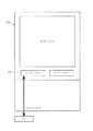
本実施の形態の表示装置としての液晶表示装置10は、図2に示すように、表示画面としての表示パネル1を有しているとともに、この表示パネル1を駆動するためにソースドライバ2及びゲートドライバ3を備えている。上記ソースドライバ2には、コマンドインターフェース(I/F)4を介してパーソナルコンピュータ(PC)5が接続されており、これにより、パーソナルコンピュータ(PC)5からの指示に基く表示が表示パネル1にて行われるようになっている。
【0036】
上記の液晶表示装置10は、図示しないバックライトをOFFして外部光を用いる反射方式(仮に「モード1」と呼ぶ)と、暗い場所ではバックライトによる透過方式(仮に「モード2」と呼ぶ)の両方の表示モードが可能な半透過方式となっている。
【0037】
本実施の形態では、上記の液晶表示装置10には、出力端子設定手段としての不揮発メモリ6が設けられており、この不揮発メモリ6には、反射用データ6a及び透過用データ6bが格納されている。
【0038】
上記不揮発メモリ6は、上記ソースドライバ2に接続されており、これによって、不揮発メモリ6に記憶された反射用データ6a及び透過用データ6bがソースドライバ2にて使用できるようになっている。すなわち、この不揮発メモリ6は、例えばパーソナルコンピュータ(PC)5からコマンドインターフェース(I/F)4を介したアクセスが可能となっている。なお、コマンドインターフェース(I/F)4とは、80系CPUに代表されるnビット(nは、8、9、16等)のCPUバスインターフェースをいう。
【0039】
上記不揮発メモリ6の反射用データ6a及び透過用データ6bには、液晶表示装置10の表示モードそれぞれに対応するγ補正値が記憶されている。
【0040】
これにより、モード1からモード2への変更や、その逆等、表示モードの変化に連動して対応する反射用データ6a及び透過用データ6bの最適値をコマンドにより切り替えることによって、液晶表示装置10の動作中でも容易に上記反射用データ6a及び透過用データ6bをその最適値に補正することができる。この結果、階調表示が正しくなり、屋内、屋外問わず表示画像の品位向上が可能となるようになっている。
【0041】
また、上記の不揮発メモリ6を搭載することによって、上記説明以外の表示モードでγ特性の切り替えが必要な場合でも、複雑な回路を組むことなく容易にγ特性を最適値に設定できるので、非常に実用的な液晶表示装置10となる。
【0042】
ここで、上記液晶表示装置10において、上述したような各表示モードで最適なγ補正を行うための具体的な構成及びその方法について述べる。
【0043】
まず、図1(a)(b)に示すように、本実施の形態の階調基準電位生成手段としての階調基準電位生成回路20は、必要階調数64の例えば16倍の階調数における各階調基準電位を出力すべく1個のラダー抵抗器7による抵抗分圧比で決定される出力端子11の群を備えている。
【0044】
また、上記出力端子11の群における各出力端子11には、選択手段としての各セレクタ12…が接続されるとともに、この各セレクタ12…には、出力端子設定手段としての不揮発メモリ6が接続されている。
【0045】
そして、上記不揮発メモリ6は、表示モードに応じた必要階調数64における各階調レベルの出力端子11を設定するものである一方、セレクタ12…は、上記不揮発メモリ6にて設定された出力端子11から、入力階調信号に対する出力端子11を選択して取り出して表示パネル1に電圧印加するようになっている。
【0046】
すなわち、本実施の形態では、γ補正の1つの方法として、図1(a)(b)に示すように、カラーパレット(Color palette)を用いる方法を採用している。
【0047】
具体的には、本実施の形態の階調基準電位生成回路20は、例えば64階調を実現するために、この64階調よりも多い階調区分を用意しておき、その中から任意の64階調を選択する。なお、本実施の形態では、必要階調数として64個の場合について説明しているが、必ずしもこれに限ることはない。
【0048】
詳細には、同図(a)に示すように、1024段階に区切った出力端子11…から任意の64個の出力端子11をそれぞれのセレクタ12…にて選ぶことによって、最適な64階調を実現する。この場合に、いずれの64個の出力端子11を選択するかについては、図1(b)に示すように、不揮発メモリ6にデータが格納されているので、反射方式及び透過方式に応じた出力端子11が選択される。なお、本実施の形態では、階調基準電位生成回路20は、必要階調数として64個に対して、出力端子11は1024個となっている。しかし、必ずしもこれに限らず、必要階調数のN倍(Nは2以上の整数)の階調数における各階調基準電位を出力するものであればよい。本実施の形態では、上述したように、N=1024/64=16である。なお、このNは、γ補正の高精度化の観点からは、多い方がよい。
【0049】
この方法においては、図3(a)(b)に示すように、1ドット毎に表示を行う点順次方式であれば、高性能なD/A変換器(DAC:Digital−to−Analog Converter)13を用いて1024階調分の出力端子11…を切り替えれば良い。
【0050】
しかし、図4(a)(b)に示すように、1水平期間(1H)毎の表示を行う線順次方式では、ソースライン14毎にD/A変換器(DAC)13を用意する必要があるので、ソースライン数×1024階調分の出力端子11…を用意する必要があり、出力端子11…を作りこむのが大変になるので現実的ではない。
【0051】
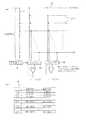
そこで、もう少し簡便に実現するものとして、図5(a)に示すように、階調基準電位生成手段としての階調基準電位生成回路30には、電源電圧(VOH−VOL)を分圧すべく、一方には、2つの可変抵抗器15・16とそれら2つの可変抵抗器15・16の間に設けられて必要階調レベル数の階調基準電位を出力するラダー抵抗器7が設けられ、他方には、2つの可変抵抗器17・18とそれら2つの可変抵抗器17・18の間に設けられて必要階調レベル数の階調基準電位を出力するラダー抵抗器7が設けられている。
【0052】
すなわち、上記2組のラダー抵抗器7・7は、正極性の階調基準電位生成と逆極性の階調基準電位生成とに用いられるようになっている。したがって、同図において左側のラダー抵抗器7からは、正極性の階調基準電位であるV0+〜V63+が取り出される一方、同図において右側のラダー抵抗器7からは、逆極性の階調基準電位であるV63−〜V0−が取り出されるようになっている。
【0053】
また、階調基準電位生成回路30には、各可変抵抗器15〜18の抵抗値R1〜R4を設定すべく、表示モード毎の抵抗値設定データが記憶された不揮発メモリ6が設けられている。
【0054】
上記の階調基準電位生成回路30では、可変抵抗器15〜18を設けておき、これら可変抵抗器15〜18の抵抗値を変えてV0〜V63の電圧を変化させるようにしておく。上記可変抵抗器15〜18の抵抗値をどのように変えるかについては、図5(b)に示すように、不揮発メモリ6に反射方式の場合には抵抗値R1・R2・R3・R4が選択され、透過方式の場合には抵抗値R1’・R2’・R3’・R4’が選択されるようになっている。
【0055】
これによって、図6に示すように、階調特性を変化させ、入力階調信号に対して最適な出力電圧を得ることができる。
【0056】
このように、実際には全ての階調信号に対して1つずつ設定していくのは現実的では無いため、いくつかのパターンのγ補正値を不揮発メモリ6に用意しておき、最適なものを用いるのが好ましい。
【0057】
このように、本実施の形態の液晶表示装置10では、階調基準電位生成回路20には、必要階調数64の例えば16倍の階調数1024における各階調基準電位を出力すべく1個のラダー抵抗器7による抵抗分圧比で決定される出力端子11の群が備えられている。
【0058】
したがって、ラダー抵抗器7は1個であるので、複数設ける場合に比べて階調基準電位生成回路20が大きくなることはない。
【0059】
また、出力端子11の群は、必要階調数64の例えば16倍の階調数1024における各階調基準電位が用意される。したがって、必要階調数64での階調レベルに対して、さらに、細かい階調レベルの階調基準電位が出力されているので、これを選択することにより、精度よくγ補正を行うことができる。
【0060】
また、不揮発メモリ6は、メモリからなっているとともに、出力端子11群から、表示モードに応じた必要階調数64における各階調レベルの出力端子11を設定するとともに、セレクタ12は、上記不揮発メモリ6にて設定された出力端子11から、入力階調信号に対する出力端子11を選択して取り出して表示パネル1に電圧印加する。
【0061】
したがって、液晶表示装置10にコマンドインターフェース4によるアクセスが可能な不揮発メモリ6を設置して、液晶表示装置10の複数の表示モードそれぞれに対応するγ補正値が記憶されている。
【0062】
この結果、階調表示が正しくなり、屋内、屋外問わず表示画像の品位向上が可能となる。
【0063】
したがって、表示モードの切り替えに起因する階調表示の変化を抑えるために、精度の良く各表示モードにおける階調信号−輝度特性を同じにし得る液晶表示装置10を提供することができる。
【0064】
また、本実施の形態の液晶表示装置10では、メモリは不揮発性にてなるので、液晶表示装置10をOFFしてもメモリに記憶された内容が消えることはない。
【0065】
また、不揮発メモリ6には、表示モード毎に該表示モードに応じた必要階調数64における各階調レベルに対する出力端子設定データが記憶されているので、この出力端子設定データによって、容易に表示モード毎の所望の各階調レベルに対する出力端子11を設定することができる。
【0066】
また、不揮発メモリ6を搭載することによって、表示モードでγ特性の切り替えが必要な場合でも、複雑な回路を組むことなく容易にγ特性を最適値に設定できるので、非常に実用的な液晶表示装置10を提供することができる。
【0067】
なお、前記特許文献1との違いは、本実施の形態の液晶表示装置10では、階調特性を決定するラダー抵抗器7を複数本持たないこと、不揮発メモリ6を有していること、不揮発性メモリの設定を基に出力端子11の値を制御している点が挙げられる。したがって、本実施の形態の液晶表示装置10では、不揮発メモリ6を有することによって、設定変更も極めて簡単である。
【0068】
したがって、設計値と実際のパネル特性のズレや、設計途上でのパネル特性の変更等に対して容易に設定変更が可能である。
【0069】
また、本実施の形態の液晶表示装置10では、階調基準電位生成回路30は、電源電圧(VOH−VOL)を分圧すべく2つの可変抵抗器とそれら2つの可変抵抗器の間に設けられて必要階調レベル数の階調基準電位を出力するラダー抵抗器7との組み合わせを2組備えている。そして、階調基準電位生成回路30には、各可変抵抗器15〜18の抵抗値を設定すべく、表示モード毎の抵抗値設定データが記憶された不揮発メモリ6が設けられているので、この不揮発メモリ6の抵抗値設定データに基いて、可変抵抗器15〜18の抵抗値が設定される。したがって、この不揮発メモリ6の抵抗値設定データを変更することにより、実質的に、任意の階調基準電位を出力することができる。
【0070】
したがって、表示モードの切り替えに起因する階調表示の変化を抑えるために、精度の良く各表示モードにおける階調信号−輝度特性を同じにし得る表示装置を提供することができる。
【0071】
また、本実施の形態の液晶表示装置10では、2組のラダー抵抗器7・7は、正極性の階調基準電位生成と逆極性の階調基準電位生成とに用いられる。すなわち、例えば、液晶表示装置10においては、正極性の階調基準電位と逆極性の階調基準電位とを印加する必要がある。
【0072】
この点、本実施の形態では、2つの2組の可変抵抗器15〜18つまり計4個の可変抵抗器15〜18を設けることによって、正極性の階調基準電位生成と逆極性の階調基準電位生成とにおいて、任意の階調レベルの階調基準電位を生成することができる。
【0073】
したがって、階調基準電位生成回路30をコンパクトにしつつ、かつ不揮発メモリ6に書き込む情報量も非常に小さくてすむ。
【0074】
なお、前記引用文献2及び引用文献3との違いは、引用文献2及び引用文献3では階調特性を滑らかに変えるには、階調補正電圧の入力ポイントを多く(実施例では10ポイント、実際は+書き込み/−書き込み用でその倍の20ポイント必要となる)持たなければならないのに対して、本実施の形態の液晶表示装置10では、2ポイント(+書き込み/−書き込み用合わせても4ポイント必要となる)のデータで済むため、不揮発メモリ6に書き込む情報量が非常に小さくてすむ。
【0075】
【発明の効果】
本発明の表示装置は、以上のように、電源電圧を分圧すべく2つの可変抵抗器とそれら2つの可変抵抗器の間に設けられて必要階調レベル数の階調基準電位を出力するラダー抵抗器との組み合わせを2組備えた階調基準電位生成手段が設けられているととともに、上記階調基準電位生成手段には、各可変抵抗器の抵抗値を設定すべく、表示モード毎の抵抗値設定データが記憶された不揮発性メモリが設けられているものである。
【0076】
それゆえ、不揮発性メモリの抵抗値設定データを変更することにより、実質的に、任意の階調基準電位を出力することができる。
【0077】
したがって、表示モードの切り替えに起因する階調表示の変化を抑えるために、精度の良く各表示モードにおける階調信号−輝度特性を同じにし得る表示装置を提供することができるという効果を奏する。
【0078】
また、本発明の表示装置は、上記記載の表示装置において、前記2組のラダー抵抗器は、正極性の階調基準電位生成と逆極性の階調基準電位生成とに用いられるものである。
【0079】
それゆえ、2つの2組の可変抵抗器つまり計4個の可変抵抗器を設けることによって、正極性の階調基準電位生成と逆極性の階調基準電位生成とにおいて、任意の階調レベルの階調基準電位を生成することができる。
【0080】
したがって、階調基準電位生成手段をコンパクトにしつつ、かつ不揮発性メモリに書き込む情報量も非常に小さくてすむという効果を奏する。
【0081】
また、本発明の表示装置は、以上のように、必要階調数のN倍(Nは2以上の整数)の階調数における各階調基準電位を出力すべく1個のラダー抵抗器による抵抗分圧比で決定される出力端子群を備えた階調基準電位生成手段と、上記出力端子群から、表示モードに応じた必要階調数における各階調レベルの出力端子を設定するメモリからなる出力端子設定手段と、上記出力端子設定手段にて設定された出力端子から、入力階調信号に対する出力端子を選択して取り出して表示画面に電圧印加する選択手段とが設けられているものである。
【0082】
それゆえ、ラダー抵抗器は1個であるので、複数設ける場合に比べて階調基準電位生成手段が大きくなることはない。
【0083】
また、出力端子群は、必要階調数での階調レベルに対して、さらに、細かい階調レベルの階調基準電位が出力されているので、これを選択することにより、精度よくγ補正を行うことができる。
【0084】
また、出力端子設定手段は、メモリからなっているとともに、出力端子群から、表示モードに応じた必要階調数における各階調レベルの出力端子を設定するとともに、選択手段は、上記出力端子設定手段にて設定された出力端子から、入力階調信号に対する出力端子を選択して取り出して表示画面に電圧印加する。
【0085】
したがって、例えば、表示装置にコマンドインターフェースによるアクセスが可能な不揮発性のメモリを設置して、表示装置の複数の表示モードそれぞれに対応するγ補正値を記憶させておく。
【0086】
この結果、階調表示が正しくなり、屋内、屋外問わず表示画像の品位向上が可能となる。
【0087】
したがって、表示モードの切り替えに起因する階調表示の変化を抑えるために、精度の良く各表示モードにおける階調信号−輝度特性を同じにし得る表示装置を提供することができるという効果を奏する。
【図面の簡単な説明】
【図1】本発明における液晶表示装置の実施の一形態を示すものであり、(a)は階調基準電位生成回路の要部の構成を示すブロック図であり、(b)は不揮発メモリに記録されているデータを示す説明図である。
【図2】上記液晶表示装置の全体概略構成を示すブロック図である。
【図3】(a)(b)は点順次方式の階調基準電位生成回路を示すブロック図である。
【図4】(a)(b)は線順次方式の階調基準電位生成回路を示すブロック図である。
【図5】(a)は上記液晶表示装置における他の階調基準電位生成回路の要部の構成を示すブロック図であり、(b)は不揮発メモリに記録されているデータを示す説明図である。
【図6】入力階調信号と出力電圧との関係を示すグラフである。
【図7】入力階調信号と輝度との関係を示すグラフである。
【図8】従来の液晶表示装置におけるγ補正回路の構成を示すブロック図である。
【図9】上記液晶表示装置の全体概略構成を示すブロック図である。
【図10】上記液晶表示装置における透過方式及び反射方式の入力階調信号と輝度との関係を示すグラフである。
【図11】上記液晶表示装置における透過方式及び反射方式の印加電圧と透過率との関係を示すグラフである。
【図12】上記液晶表示装置における透過方式及び反射方式の入力階調信号と印加電圧との関係を示すグラフである。
【図13】理想状態の液晶表示装置における透過方式及び反射方式の入力階調信号と輝度との関係を示すグラフである。
【図14】従来の他の液晶表示装置におけるγ補正回路の構成を示すブロック図である。
【図15】従来のさらに他の液晶表示装置におけるγ補正回路の構成を示すブロック図である。
【符号の説明】
1 表示パネル(表示画面)
6 不揮発メモリ(出力端子設定手段)
7 ラダー抵抗器
11 出力端子
12 セレクタ(選択手段)
15〜18 可変抵抗器
20 階調基準電位生成回路(階調基準電位生成手段)
30 階調基準電位生成回路(階調基準電位生成手段)[0001]
TECHNICAL FIELD OF THE INVENTION
The present invention provides both a reflective display and a transmissive display and a transflective liquid crystal display in which the relationship between the applied voltage and the transmissivity or the relationship between the applied voltage and the reflectivity differs in the display mode between the reflective display and the transmissive display. The present invention relates to a display device such as a device.
[0002]
[Prior art]
In a display device such as a liquid crystal display device, it is generally considered that a gradation characteristic is such that output luminance is linear with respect to an input gradation signal. Here, the characteristic of the input gradation signal value versus the output luminance is called a γ characteristic. Specifically, the γ characteristic means that the luminance L of the display device changes in proportion to the γ power of the input gradation signal value E to the display device. When this is expressed by an equation, L = KEγ (Generally, γ = 2.2 to 3, K is a constant).
[0003]
As described above, many display devices have an output luminance with respect to an input gradation signal which is not linear and has a relationship of the above-mentioned γ characteristic. Therefore, a correct gradation display cannot be performed as it is.
[0004]
In view of this, in the display device, as shown as “γ inverse characteristic of a general image” in FIG. It is necessary to make correction using the γ power. This is called gamma correction. As a result, as shown as “correct gradation characteristics” in the drawing, a relationship is obtained in which the output luminance is linear with respect to the input gradation signal where L = KE (K is a constant).
[0005]
Incidentally, in order to obtain a γ characteristic corresponding to the γ inverse characteristic, a γ correction circuit of a display device is used as shown in FIG. In this gamma correction circuit, in order to realize 64 gradations, each selector selects any one of the 64 output terminals from 64 output terminals divided into 64 steps, thereby realizing the optimum 64 gradations. Thereby, a correct gradation display can be performed. Note that the γ correction circuit is built in the
[0006]
In the above-mentioned conventional liquid crystal display device, once the optimum value of the γ correction is set once, it is impossible to change it during the operation of the liquid crystal display device, but there is no problem when the display mode is unchanged.
[0007]
However, in recent years, in order to reduce power consumption in a bright place, in order to reduce power consumption, a backlight system is turned off and external light is used (tentatively called “
[0008]
In the transflective liquid crystal display device, when switching from the transmissive type to the reflective type, as shown in FIG. 10, since the gradation-luminance characteristics do not completely match, the appearance of the same image is different. This is because, as shown in FIG. 11, the applied voltage (V) -transmittance (T) characteristics do not match due to the difference between transmission and reflection. Although FIG. 2 illustrates the characteristic of applied voltage (V) -transmittance (T), the same can be said for the relationship of applied voltage (V) -reflectance.
[0009]
Further, there is a need to change the gradation display in each display mode. In other words, one tone setting gives the user a sense of discomfort.
[0010]
Therefore, as shown in FIG. 12, a plurality of characteristic curves of the gradation-voltage application characteristics of the source driver are prepared, and the display modes are switched in conjunction with each other. Although two settings are shown in the drawing, it is needless to say that two or more settings may be provided and the user can select from the two settings. As a result, as shown in FIG. 13, the gradation-luminance characteristics can be completely matched between the time of transmission and the time of reflection.
[0011]
As a conventional display device in which the gradation level can be changed depending on the display mode, for example, in
[0012]
Further, for example, in
[0013]
[Patent Document 1]
JP-A-2000-193936 (published on July 14, 2000)
[0014]
[Patent Document 2]
JP-A-10-333648 (published on December 18, 1998)
[0015]
[Patent Document 3]
JP-A-63-38989 (released on February 19, 1988)
[0016]
[Problems to be solved by the invention]
However, among the above-mentioned conventional display devices, in
[0017]
Also in
[0018]
SUMMARY OF THE INVENTION The present invention has been made in view of the above-described conventional problems, and has as its object to suppress a change in gradation display caused by switching of a display mode, and to accurately control a gradation signal in each display mode. It is an object of the present invention to provide a display device having the same luminance characteristics.
[0019]
[Means for Solving the Problems]
The display device of the present invention performs both reflective display and transmissive display in order to solve the above problem, and the relationship between the applied voltage and the transmissivity or the applied voltage and the reflectivity is such that the reflective display and the transmissive display are different. In the transflective display device different in the display mode, two variable resistors are provided between the two variable resistors in order to divide the power supply voltage, and the required number of gradation levels is output as the gradation reference potential. A gradation reference potential generating means provided with two sets of combinations with a ladder resistor is provided, and the gradation reference potential generating means is provided with a display mode for setting the resistance value of each variable resistor. And a nonvolatile memory in which the resistance value setting data is stored.
[0020]
According to the above invention, the gray scale reference potential generating means is provided between the two variable resistors and the two variable resistors to divide the power supply voltage, and generates the required number of gray scale reference potentials. Two sets are provided in combination with the output ladder resistor. The non-volatile memory storing the resistance value setting data for each display mode is provided in the gradation reference potential generating means in order to set the resistance value of each variable resistor. The resistance value of the variable resistor is set based on the resistance value setting data. Therefore, by changing the resistance value setting data of the nonvolatile memory, a substantially arbitrary gradation reference potential can be output.
[0021]
Therefore, it is possible to provide a display device capable of accurately setting the same gray scale signal-luminance characteristic in each display mode in order to suppress a change in gray scale display caused by switching of display modes.
[0022]
In the display device according to the present invention, in the display device described above, the two sets of ladder resistors are used for generating a grayscale reference potential having a positive polarity and a grayscale reference potential having a reverse polarity. I have.
[0023]
According to the above invention, the two sets of ladder resistors are used for generating a grayscale reference potential of a positive polarity and a grayscale reference potential of an opposite polarity. That is, for example, in a liquid crystal display device, it is necessary to apply a gradation reference potential of positive polarity and a gradation reference potential of opposite polarity.
[0024]
In this regard, in the present invention, by providing two sets of variable resistors, that is, a total of four variable resistors, it is possible to arbitrarily generate a grayscale reference potential of positive polarity and a grayscale reference potential of opposite polarity. A gradation reference potential of a gradation level can be generated.
[0025]
Therefore, the amount of information to be written in the nonvolatile memory can be very small while the gradation reference potential generating means is made compact.
[0026]
Further, in order to solve the above-described problems, the display device of the present invention performs both the reflective display and the transmissive display, and determines whether the relationship between the applied voltage and the transmissivity or the relationship between the applied voltage and the reflectivity is different from the reflective display and the transmissive display. In a transflective display device different in display mode from display, one ladder resistor is used to output each gradation reference potential at N times (N is an integer of 2 or more) required gradations. A gradation reference potential generating means having an output terminal group determined by a resistance voltage division ratio, and an output comprising a memory for setting output terminals of each gradation level in a required number of gradations according to a display mode from the output terminal group. Terminal setting means, and selecting means for selecting and taking out an output terminal for an input gradation signal from the output terminals set by the output terminal setting means and applying a voltage to a display screen, I .
[0027]
According to the above invention, one ladder resistor is provided in the gradation reference potential generating means so as to output each gradation reference potential at N times the number of necessary gradations (N is an integer of 2 or more). The output terminal group is determined by the resistance voltage division ratio according to
[0028]
Therefore, since there is only one ladder resistor, the gray scale reference potential generating means does not become larger than when a plurality of ladder resistors are provided.
[0029]
Further, as the output terminal group, each gradation reference potential is prepared for N times (N is an integer of 2 or more) the required number of gradations. Therefore, since a gradation reference potential of a finer gradation level is output with respect to the gradation level of the required number of gradations, by selecting this, the γ correction can be performed with high accuracy.
[0030]
The output terminal setting means comprises a memory, and sets an output terminal of each gradation level in a required number of gradations according to the display mode from the output terminal group. An output terminal corresponding to the input gradation signal is selected and taken out from the output terminals set in the above step, and a voltage is applied to the display screen.
[0031]
Therefore, for example, a non-volatile memory accessible by a command interface is installed in the display device, and the γ correction values corresponding to each of the plurality of display modes of the display device are stored.
[0032]
As a result, the gradation display is correct, and the quality of the displayed image can be improved both indoors and outdoors.
[0033]
Therefore, it is possible to provide a display device capable of accurately setting the same gray scale signal-luminance characteristic in each display mode in order to suppress a change in gray scale display caused by switching of display modes.
[0034]
BEST MODE FOR CARRYING OUT THE INVENTION
An embodiment of the present invention will be described below with reference to FIGS. In this embodiment mode, a liquid crystal display device as a display device will be described. However, the display device is not necessarily limited to the liquid crystal display device. Other display devices may be used as long as they differ from the display.
[0035]
As shown in FIG. 2, a liquid
[0036]
The above-described liquid
[0037]
In the present embodiment, the above-described liquid
[0038]
The
[0039]
The gamma correction values corresponding to the display modes of the liquid
[0040]
Thus, by switching the optimum values of the reflection data 6a and the transmission data 6b corresponding to the change of the display mode, such as the change from the
[0041]
Also, by mounting the above-mentioned
[0042]
Here, a specific configuration and a method for performing the optimum γ correction in each of the above-described display modes in the liquid
[0043]
First, as shown in FIGS. 1A and 1B, the gray scale reference
[0044]
Each of the output terminals 11 in the group of the output terminals 11 is connected to each of the
[0045]
The
[0046]
That is, in the present embodiment, as one method of the γ correction, as shown in FIGS. 1A and 1B, a method using a color palette is adopted.
[0047]
Specifically, the gray-scale reference
[0048]
More specifically, as shown in FIG. 7A, by selecting arbitrary 64 output terminals 11 from the output terminals 11 divided into 1024 stages by the
[0049]
In this method, as shown in FIGS. 3A and 3B, a high-performance D / A converter (DAC: Digital-to-Analog Converter) can be used if a dot-sequential system that performs display for each dot is used. 13, the output terminals 11 for 1024 gradations may be switched.
[0050]
However, as shown in FIGS. 4A and 4B, in the line-sequential system in which display is performed for each horizontal period (1H), it is necessary to prepare a D / A converter (DAC) 13 for each
[0051]
Therefore, as a simpler implementation, as shown in FIG. 5A, a gradation reference
[0052]
That is, the two sets of
[0053]
Further, the gradation reference
[0054]
In the gradation reference
[0055]
As a result, as shown in FIG. 6, it is possible to change the gradation characteristics and obtain an optimum output voltage for the input gradation signal.
[0056]
As described above, since it is not realistic to set one by one for all the gradation signals, the gamma correction values of some patterns are prepared in the
[0057]
As described above, in the liquid
[0058]
Therefore, since the number of the
[0059]
For the group of output terminals 11, each gradation reference potential is prepared for 1024 gradations, for example, 16 times the necessary gradation number 64. Therefore, since a gradation reference potential of a finer gradation level is output with respect to the gradation level with the necessary gradation number of 64, by selecting this, the γ correction can be performed with high accuracy. .
[0060]
The
[0061]
Therefore, the
[0062]
As a result, the gradation display is correct, and the quality of the displayed image can be improved both indoors and outdoors.
[0063]
Therefore, it is possible to provide the liquid
[0064]
Further, in the liquid
[0065]
Further, since the
[0066]
Also, by mounting the
[0067]
The difference from
[0068]
Therefore, it is possible to easily change the setting with respect to a deviation between the design value and the actual panel characteristic, a change in the panel characteristic during the design process, and the like.
[0069]
Further, in the liquid
[0070]
Therefore, it is possible to provide a display device capable of accurately setting the same gray scale signal-luminance characteristic in each display mode in order to suppress a change in gray scale display caused by switching of display modes.
[0071]
Further, in the liquid
[0072]
In this regard, in this embodiment, by providing two sets of
[0073]
Therefore, the gray scale reference
[0074]
The difference between the cited
[0075]
【The invention's effect】
As described above, the display device of the present invention is provided with two variable resistors for dividing the power supply voltage and a ladder that is provided between the two variable resistors and outputs the required number of gradation levels as the gradation reference potential. A gray scale reference potential generating means having two sets of combinations with resistors is provided, and the gray scale reference potential generating means is provided for each display mode in order to set the resistance value of each variable resistor. A nonvolatile memory in which resistance value setting data is stored is provided.
[0076]
Therefore, by changing the resistance value setting data of the nonvolatile memory, a substantially arbitrary gradation reference potential can be output.
[0077]
Therefore, in order to suppress a change in gray scale display due to the switching of the display mode, it is possible to provide a display device capable of making the gray scale signal-luminance characteristics in each display mode the same with high accuracy.
[0078]
Further, in the display device according to the present invention, in the display device described above, the two sets of ladder resistors are used for generating a grayscale reference potential having a positive polarity and a grayscale reference potential having a reverse polarity.
[0079]
Therefore, by providing two two sets of variable resistors, that is, a total of four variable resistors, it is possible to generate an arbitrary gradation level between the generation of a positive gradation reference potential and the generation of a reverse gradation reference potential. A gradation reference potential can be generated.
[0080]
Therefore, there is an effect that the amount of information to be written in the nonvolatile memory can be very small while the gray scale reference potential generating means is made compact.
[0081]
Further, as described above, the display device of the present invention uses one ladder resistor to output each gradation reference potential at N times (N is an integer of 2 or more) required gradations. An output terminal comprising a gray scale reference potential generating means having an output terminal group determined by a voltage division ratio, and a memory for setting, from the output terminal group, an output terminal of each gray level in a required number of gray levels according to a display mode. There is provided setting means and selection means for selecting and taking out an output terminal for an input gradation signal from the output terminals set by the output terminal setting means and applying a voltage to a display screen.
[0082]
Therefore, since there is only one ladder resistor, the gray scale reference potential generating means does not become larger than when a plurality of ladder resistors are provided.
[0083]
Further, the output terminal group outputs a gradation reference potential of a finer gradation level with respect to the gradation level of the required number of gradations. It can be carried out.
[0084]
The output terminal setting means comprises a memory, and sets an output terminal of each gradation level in a required number of gradations according to the display mode from the output terminal group. An output terminal corresponding to the input gradation signal is selected and taken out from the output terminals set in the above step, and a voltage is applied to the display screen.
[0085]
Therefore, for example, a non-volatile memory accessible by a command interface is installed in the display device, and the γ correction values corresponding to each of the plurality of display modes of the display device are stored.
[0086]
As a result, the gradation display is correct, and the quality of the displayed image can be improved both indoors and outdoors.
[0087]
Therefore, in order to suppress a change in gray scale display due to the switching of the display mode, it is possible to provide a display device capable of making the gray scale signal-luminance characteristics in each display mode the same with high accuracy.
[Brief description of the drawings]
FIGS. 1A and 1B show an embodiment of a liquid crystal display device according to the present invention, in which FIG. 1A is a block diagram showing a configuration of a main part of a gradation reference potential generation circuit, and FIG. FIG. 4 is an explanatory diagram showing recorded data.
FIG. 2 is a block diagram showing an overall schematic configuration of the liquid crystal display device.
FIGS. 3A and 3B are block diagrams showing a gradation reference potential generation circuit of a dot sequential method.
FIGS. 4A and 4B are block diagrams showing a gradation reference potential generation circuit of a line sequential system.
FIG. 5A is a block diagram illustrating a configuration of a main part of another gradation reference potential generation circuit in the liquid crystal display device, and FIG. 5B is an explanatory diagram illustrating data recorded in a nonvolatile memory; is there.
FIG. 6 is a graph showing a relationship between an input gradation signal and an output voltage.
FIG. 7 is a graph showing a relationship between an input gradation signal and luminance.
FIG. 8 is a block diagram illustrating a configuration of a gamma correction circuit in a conventional liquid crystal display device.
FIG. 9 is a block diagram illustrating an overall schematic configuration of the liquid crystal display device.
FIG. 10 is a graph showing a relationship between input gradation signals of a transmission system and a reflection system and luminance in the liquid crystal display device.
FIG. 11 is a graph showing a relationship between an applied voltage and a transmittance in a transmission mode and a reflection mode in the liquid crystal display device.
FIG. 12 is a graph showing a relationship between an input gradation signal of a transmission type and a reflection type and an applied voltage in the liquid crystal display device.
FIG. 13 is a graph showing a relationship between input gradation signals of a transmission system and a reflection system and luminance in a liquid crystal display device in an ideal state.
FIG. 14 is a block diagram illustrating a configuration of a gamma correction circuit in another conventional liquid crystal display device.
FIG. 15 is a block diagram showing a configuration of a gamma correction circuit in still another conventional liquid crystal display device.
[Explanation of symbols]
1 display panel (display screen)
6. Non-volatile memory (output terminal setting means)
7 Ladder resistor
11 Output terminal
12 Selector (selection means)
15-18 Variable resistor
20 gradation reference potential generation circuit (gradation reference potential generation means)
30 gradation reference potential generation circuit (gradation reference potential generation means)
Claims (4)
Translated fromJapanese電源電圧を分圧すべく2つの可変抵抗器とそれら2つの可変抵抗器の間に設けられて必要階調レベル数の階調基準電位を出力するラダー抵抗器との組み合わせを2組備えた階調基準電位生成手段が設けられているととともに、
上記階調基準電位生成手段には、各可変抵抗器の抵抗値を設定すべく、表示モード毎の抵抗値設定データが記憶された不揮発性メモリが設けられていることを特徴とする表示装置。While performing both display of reflection display and transmission display, in the transflective display device, the relationship between the applied voltage and the transmittance or the applied voltage and the reflectance is different in the display mode of the reflective display and the transmissive display,
A gray scale having two combinations of two variable resistors for dividing the power supply voltage and a ladder resistor provided between the two variable resistors and outputting a required number of gray scale reference potentials. With the provision of the reference potential generating means,
A display device, characterized in that the gradation reference potential generating means is provided with a non-volatile memory storing resistance value setting data for each display mode in order to set the resistance value of each variable resistor.
必要階調数のN倍(Nは2以上の整数)の階調数における各階調基準電位を出力すべく1個のラダー抵抗器による抵抗分圧比で決定される出力端子群を備えた階調基準電位生成手段と、
上記出力端子群から、表示モードに応じた必要階調数における各階調レベルの出力端子を設定するメモリからなる出力端子設定手段と、
上記出力端子設定手段にて設定された出力端子から、入力階調信号に対する出力端子を選択して取り出して表示画面に電圧印加する選択手段とが設けられていることを特徴とする表示装置。While performing both display of reflection display and transmission display, in the transflective display device, the relationship between the applied voltage and the transmittance or the applied voltage and the reflectance is different in the display mode of the reflective display and the transmissive display,
A gray scale having an output terminal group determined by a resistance voltage division ratio of one ladder resistor to output each gray scale reference potential at N times the required number of gray levels (N is an integer of 2 or more) Reference potential generating means;
Output terminal setting means comprising a memory for setting an output terminal of each gradation level at a required number of gradations according to the display mode from the output terminal group;
A display device comprising: a selection unit that selects and takes out an output terminal for an input gradation signal from the output terminals set by the output terminal setting unit and applies a voltage to a display screen.
その不揮発性のメモリには、表示モード毎に該表示モードに応じた必要階調数における各階調レベルに対する出力端子設定データが記憶されていることを特徴とする請求項3記載の表示装置。The memory is non-volatile,
4. The display device according to claim 3, wherein the non-volatile memory stores, for each display mode, output terminal setting data for each gradation level in a required number of gradations according to the display mode.
Priority Applications (8)
| Application Number | Priority Date | Filing Date | Title |
|---|---|---|---|
| JP2002322229AJP2004157288A (en) | 2002-11-06 | 2002-11-06 | Display device |
| US10/670,237US7262756B2 (en) | 2002-11-06 | 2003-09-26 | Display apparatus |
| CNB2006100959184ACN100514436C (en) | 2002-11-06 | 2003-09-30 | Display apparatus |
| CNB031434916ACN1302452C (en) | 2002-11-06 | 2003-09-30 | Display device |
| KR1020030068752AKR100749879B1 (en) | 2002-11-06 | 2003-10-02 | Display apparatus |
| TW092127424ATWI259304B (en) | 2002-11-06 | 2003-10-03 | Display apparatus |
| KR1020060038149AKR100683057B1 (en) | 2002-11-06 | 2006-04-27 | Display device |
| US11/790,140US7973752B2 (en) | 2002-11-06 | 2007-04-24 | Display apparatus |
Applications Claiming Priority (1)
| Application Number | Priority Date | Filing Date | Title |
|---|---|---|---|
| JP2002322229AJP2004157288A (en) | 2002-11-06 | 2002-11-06 | Display device |
Publications (1)
| Publication Number | Publication Date |
|---|---|
| JP2004157288Atrue JP2004157288A (en) | 2004-06-03 |
Family
ID=32171330
Family Applications (1)
| Application Number | Title | Priority Date | Filing Date |
|---|---|---|---|
| JP2002322229APendingJP2004157288A (en) | 2002-11-06 | 2002-11-06 | Display device |
Country Status (5)
| Country | Link |
|---|---|
| US (2) | US7262756B2 (en) |
| JP (1) | JP2004157288A (en) |
| KR (2) | KR100749879B1 (en) |
| CN (2) | CN100514436C (en) |
| TW (1) | TWI259304B (en) |
Cited By (9)
| Publication number | Priority date | Publication date | Assignee | Title |
|---|---|---|---|---|
| JP2006227271A (en)* | 2005-02-17 | 2006-08-31 | Seiko Epson Corp | Reference voltage selection circuit, reference voltage generation circuit, display driver, electro-optical device, and electronic apparatus |
| JP2006227272A (en)* | 2005-02-17 | 2006-08-31 | Seiko Epson Corp | Reference voltage generation circuit, display driver, electro-optical device, and electronic apparatus |
| JP2006243232A (en)* | 2005-03-02 | 2006-09-14 | Seiko Epson Corp | Reference voltage generation circuit, display driver, electro-optical device, and electronic apparatus |
| JP2006243231A (en)* | 2005-03-02 | 2006-09-14 | Seiko Epson Corp | Reference voltage generation circuit, display driver, electro-optical device, and electronic apparatus |
| JP2006243233A (en)* | 2005-03-02 | 2006-09-14 | Seiko Epson Corp | Reference voltage generation circuit, display driver, electro-optical device, and electronic apparatus |
| JP2007171997A (en)* | 2007-03-19 | 2007-07-05 | Seiko Epson Corp | Reference voltage generation circuit, display driver, electro-optical device, and electronic apparatus |
| JP2007183670A (en)* | 2007-03-19 | 2007-07-19 | Seiko Epson Corp | Reference voltage generation circuit, display driver, electro-optical device, and electronic apparatus |
| JP2008170652A (en)* | 2007-01-10 | 2008-07-24 | Nec Lcd Technologies Ltd | Transflective liquid crystal display device |
| JP2009157169A (en)* | 2007-12-27 | 2009-07-16 | Casio Comput Co Ltd | Display device |
Families Citing this family (10)
| Publication number | Priority date | Publication date | Assignee | Title |
|---|---|---|---|---|
| JP2004157288A (en)* | 2002-11-06 | 2004-06-03 | Sharp Corp | Display device |
| JP4199141B2 (en)* | 2004-02-23 | 2008-12-17 | 東芝松下ディスプレイテクノロジー株式会社 | Display signal processing device and display device |
| JP4111185B2 (en) | 2004-10-19 | 2008-07-02 | セイコーエプソン株式会社 | Electro-optical device, driving method thereof, and electronic apparatus |
| TWI401640B (en) | 2004-11-12 | 2013-07-11 | Samsung Display Co Ltd | Display device and driving method thereof |
| KR100699869B1 (en)* | 2005-10-21 | 2007-03-28 | 삼성전자주식회사 | Display driver and method for adjusting output gray voltage level |
| US7576720B2 (en)* | 2005-11-30 | 2009-08-18 | Au Optronics Corporation | Transflective liquid crystal display |
| JP4936854B2 (en)* | 2006-10-25 | 2012-05-23 | ルネサスエレクトロニクス株式会社 | Display device and display panel driver |
| JP2009222786A (en)* | 2008-03-13 | 2009-10-01 | Hitachi Displays Ltd | Liquid crystal display device |
| JP4878060B2 (en)* | 2009-11-16 | 2012-02-15 | シャープ株式会社 | Network system and management method |
| CN104091575A (en) | 2014-06-26 | 2014-10-08 | 京东方科技集团股份有限公司 | Gamma voltage generating circuit, generating method and data driver |
Family Cites Families (20)
| Publication number | Priority date | Publication date | Assignee | Title |
|---|---|---|---|---|
| JPH0519725A (en) | 1991-07-15 | 1993-01-29 | Hitachi Ltd | Color liquid crystal display |
| JP3106953B2 (en) | 1996-05-16 | 2000-11-06 | 富士電機株式会社 | Display element driving method |
| JP3338299B2 (en) | 1996-07-24 | 2002-10-28 | 大崎電気工業株式会社 | Wattmeter test bench |
| JPH1062743A (en) | 1996-08-13 | 1998-03-06 | Alps Electric Co Ltd | Liquid crystal display device and driving circuit therefor |
| US6380917B2 (en) | 1997-04-18 | 2002-04-30 | Seiko Epson Corporation | Driving circuit of electro-optical device, driving method for electro-optical device, and electro-optical device and electronic equipment employing the electro-optical device |
| JP3819113B2 (en) | 1997-06-03 | 2006-09-06 | 三菱電機株式会社 | Liquid crystal display |
| JPH1138989A (en) | 1997-07-14 | 1999-02-12 | Toshiba Corp | Speech synthesis apparatus and method |
| US6462724B1 (en)* | 1997-07-25 | 2002-10-08 | Seiko Epson Corporation | Display device and electronic equipment employing the same |
| JP3186688B2 (en) | 1998-03-19 | 2001-07-11 | 関西日本電気株式会社 | Integrated circuit device |
| JPH11333648A (en) | 1998-05-25 | 1999-12-07 | Fuji Oozx Inc | Grinder |
| US6611249B1 (en)* | 1998-07-22 | 2003-08-26 | Silicon Graphics, Inc. | System and method for providing a wide aspect ratio flat panel display monitor independent white-balance adjustment and gamma correction capabilities |
| JP2000193936A (en) | 1998-12-25 | 2000-07-14 | Casio Comput Co Ltd | Liquid crystal display |
| JP2000227608A (en) | 1999-02-05 | 2000-08-15 | Hitachi Ltd | Liquid crystal display |
| JP2001022325A (en) | 1999-07-08 | 2001-01-26 | Advanced Display Inc | Liquid crystal display device |
| JP3651371B2 (en) | 2000-07-27 | 2005-05-25 | 株式会社日立製作所 | Liquid crystal drive circuit and liquid crystal display device |
| JP3832627B2 (en) | 2000-08-10 | 2006-10-11 | シャープ株式会社 | Signal line driving circuit, image display device, and portable device |
| JP3501751B2 (en)* | 2000-11-20 | 2004-03-02 | Nec液晶テクノロジー株式会社 | Driving circuit for color liquid crystal display and display device provided with the circuit |
| JP2002366112A (en)* | 2001-06-07 | 2002-12-20 | Hitachi Ltd | Liquid crystal driving device and liquid crystal display device |
| US6744415B2 (en)* | 2001-07-25 | 2004-06-01 | Brillian Corporation | System and method for providing voltages for a liquid crystal display |
| JP2004157288A (en) | 2002-11-06 | 2004-06-03 | Sharp Corp | Display device |
- 2002
- 2002-11-06JPJP2002322229Apatent/JP2004157288A/enactivePending
- 2003
- 2003-09-26USUS10/670,237patent/US7262756B2/ennot_activeExpired - Fee Related
- 2003-09-30CNCNB2006100959184Apatent/CN100514436C/ennot_activeExpired - Fee Related
- 2003-09-30CNCNB031434916Apatent/CN1302452C/ennot_activeExpired - Fee Related
- 2003-10-02KRKR1020030068752Apatent/KR100749879B1/ennot_activeExpired - Fee Related
- 2003-10-03TWTW092127424Apatent/TWI259304B/ennot_activeIP Right Cessation
- 2006
- 2006-04-27KRKR1020060038149Apatent/KR100683057B1/ennot_activeExpired - Fee Related
- 2007
- 2007-04-24USUS11/790,140patent/US7973752B2/ennot_activeExpired - Fee Related
Cited By (11)
| Publication number | Priority date | Publication date | Assignee | Title |
|---|---|---|---|---|
| JP2006227271A (en)* | 2005-02-17 | 2006-08-31 | Seiko Epson Corp | Reference voltage selection circuit, reference voltage generation circuit, display driver, electro-optical device, and electronic apparatus |
| JP2006227272A (en)* | 2005-02-17 | 2006-08-31 | Seiko Epson Corp | Reference voltage generation circuit, display driver, electro-optical device, and electronic apparatus |
| JP2006243232A (en)* | 2005-03-02 | 2006-09-14 | Seiko Epson Corp | Reference voltage generation circuit, display driver, electro-optical device, and electronic apparatus |
| JP2006243231A (en)* | 2005-03-02 | 2006-09-14 | Seiko Epson Corp | Reference voltage generation circuit, display driver, electro-optical device, and electronic apparatus |
| JP2006243233A (en)* | 2005-03-02 | 2006-09-14 | Seiko Epson Corp | Reference voltage generation circuit, display driver, electro-optical device, and electronic apparatus |
| JP2008170652A (en)* | 2007-01-10 | 2008-07-24 | Nec Lcd Technologies Ltd | Transflective liquid crystal display device |
| US8466860B2 (en) | 2007-01-10 | 2013-06-18 | Nlt Technologies, Ltd. | Transflective type LCD device having excellent image quality |
| US9093035B2 (en) | 2007-01-10 | 2015-07-28 | Nlt Technologies, Ltd. | Transflective type LCD device having excellent image quality |
| JP2007171997A (en)* | 2007-03-19 | 2007-07-05 | Seiko Epson Corp | Reference voltage generation circuit, display driver, electro-optical device, and electronic apparatus |
| JP2007183670A (en)* | 2007-03-19 | 2007-07-19 | Seiko Epson Corp | Reference voltage generation circuit, display driver, electro-optical device, and electronic apparatus |
| JP2009157169A (en)* | 2007-12-27 | 2009-07-16 | Casio Comput Co Ltd | Display device |
Also Published As
| Publication number | Publication date |
|---|---|
| US7262756B2 (en) | 2007-08-28 |
| CN100514436C (en) | 2009-07-15 |
| KR20060055496A (en) | 2006-05-23 |
| KR20040040341A (en) | 2004-05-12 |
| US20070195039A1 (en) | 2007-08-23 |
| CN1499476A (en) | 2004-05-26 |
| CN1873765A (en) | 2006-12-06 |
| US20040085635A1 (en) | 2004-05-06 |
| KR100683057B1 (en) | 2007-02-15 |
| TW200408869A (en) | 2004-06-01 |
| US7973752B2 (en) | 2011-07-05 |
| TWI259304B (en) | 2006-08-01 |
| KR100749879B1 (en) | 2007-08-21 |
| CN1302452C (en) | 2007-02-28 |
Similar Documents
| Publication | Publication Date | Title |
|---|---|---|
| KR100683057B1 (en) | Display device | |
| KR100329286B1 (en) | LCD driving circuit and LCD | |
| JP2761128B2 (en) | Liquid crystal display | |
| JP4638182B2 (en) | LIQUID CRYSTAL DISPLAY DEVICE, METHOD FOR DRIVING THE SAME AND DEVICE THEREOF | |
| CN100440277C (en) | Display device and drive circuit for display | |
| JP5313804B2 (en) | Liquid crystal display | |
| US8514158B2 (en) | Liquid crystal driving device | |
| JP2001306036A (en) | Liquid crystal display device, monochrome liquid crystal display device, controller, image conversion method, and image display method | |
| JP2008129584A (en) | Liquid crystal display device and driving method thereof | |
| CN115053284B (en) | Dynamic pixel modulation | |
| US5859633A (en) | Gradation driving circuit of liquid crystal display | |
| US7443369B2 (en) | Liquid crystal display device and an optimum gradation voltage setting apparatus thereof | |
| JPH0968695A (en) | Gray scale voltage generation circuit and liquid crystal display device | |
| CN107808646A (en) | Display driver, electro-optical device, the control method of electronic equipment and display driver | |
| JP4874931B2 (en) | Display device | |
| KR20090015196A (en) | Display device and driving method thereof | |
| JP2019028291A (en) | Display driver, display controller, electro-optic device, and electronic apparatus | |
| US6580410B1 (en) | Liquid crystal display | |
| JP4520384B2 (en) | Gradation display method for liquid crystal display device | |
| KR100864978B1 (en) | Gamma Compensation Method and Apparatus for LCD | |
| KR101032437B1 (en) | Driving Method and Driving Device of Liquid Crystal Display | |
| JP2006163290A (en) | Image display device | |
| KR20060120899A (en) | Display device and driving device thereof | |
| CN101770749A (en) | Method and device for adjusting gray scale of SCTN type liquid crystal display | |
| JP2009128461A (en) | Liquid crystal display device and driving method thereof |
Legal Events
| Date | Code | Title | Description |
|---|---|---|---|
| A621 | Written request for application examination | Free format text:JAPANESE INTERMEDIATE CODE: A621 Effective date:20050525 | |
| A977 | Report on retrieval | Free format text:JAPANESE INTERMEDIATE CODE: A971007 Effective date:20080710 | |
| A131 | Notification of reasons for refusal | Free format text:JAPANESE INTERMEDIATE CODE: A131 Effective date:20080715 | |
| A521 | Written amendment | Free format text:JAPANESE INTERMEDIATE CODE: A523 Effective date:20080904 | |
| RD02 | Notification of acceptance of power of attorney | Free format text:JAPANESE INTERMEDIATE CODE: A7422 Effective date:20080904 | |
| A131 | Notification of reasons for refusal | Free format text:JAPANESE INTERMEDIATE CODE: A131 Effective date:20091104 | |
| A02 | Decision of refusal | Free format text:JAPANESE INTERMEDIATE CODE: A02 Effective date:20100309 |