JP2004153367A - High frequency module, and mode converting structure and method - Google Patents
High frequency module, and mode converting structure and methodDownload PDFInfo
- Publication number
- JP2004153367A JP2004153367AJP2002313853AJP2002313853AJP2004153367AJP 2004153367 AJP2004153367 AJP 2004153367AJP 2002313853 AJP2002313853 AJP 2002313853AJP 2002313853 AJP2002313853 AJP 2002313853AJP 2004153367 AJP2004153367 AJP 2004153367A
- Authority
- JP
- Japan
- Prior art keywords
- waveguide
- mode
- electromagnetic wave
- magnetic field
- tem
- Prior art date
- Legal status (The legal status is an assumption and is not a legal conclusion. Google has not performed a legal analysis and makes no representation as to the accuracy of the status listed.)
- Pending
Links
Images
Classifications
- H—ELECTRICITY
- H01—ELECTRIC ELEMENTS
- H01P—WAVEGUIDES; RESONATORS, LINES, OR OTHER DEVICES OF THE WAVEGUIDE TYPE
- H01P3/00—Waveguides; Transmission lines of the waveguide type
- H01P3/12—Hollow waveguides
- H01P3/121—Hollow waveguides integrated in a substrate
- H—ELECTRICITY
- H01—ELECTRIC ELEMENTS
- H01P—WAVEGUIDES; RESONATORS, LINES, OR OTHER DEVICES OF THE WAVEGUIDE TYPE
- H01P5/00—Coupling devices of the waveguide type
- H01P5/08—Coupling devices of the waveguide type for linking dissimilar lines or devices
- H01P5/10—Coupling devices of the waveguide type for linking dissimilar lines or devices for coupling balanced lines or devices with unbalanced lines or devices
- H01P5/107—Hollow-waveguide/strip-line transitions
Landscapes
- Control Of Motors That Do Not Use Commutators (AREA)
Abstract
Description
Translated fromJapanese【0001】
【発明の属する技術分野】
本発明は、マイクロ波またはミリ波などの高周波帯域の信号の伝搬に用いられる高周波モジュール、ならびに異なる導波路間でのモード変換を行うためのモード変換構造および方法に関する。
【0002】
【従来の技術】
従来、マイクロ波帯やミリ波帯等の高周波信号を伝送するための伝送路としては、ストリップ線路、マイクロストリップ線路、同軸線路、導波管、および誘電体導波管などが知られている。これらはまた、高周波用の共振器およびフィルタを構成するものとして知られている。また、これら高周波用の構成要素をモジュール化したものとしては、MMIC(モノリシックマイクロ波集積回路)などがある。以下、高周波用の伝送路およびフィルタなどを構成するマイクロストリップ線路、および導波管などを総称して、導波路と呼ぶ。
【0003】
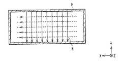
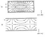
ここで、導波路における電磁波の伝搬モードについて説明する。図18(A),(B)は、矩形導波管におけるTEモード(TE10モード)と呼ばれる状態での電界分布(同図(A))と磁界分布(同図(B))とを示している。図18(A),(B)において、断面S1〜S5の位置はそれぞれ対応している。また図19には、断面S1における電磁界分布を示す。これらの図に示したように、断面方向にのみ電界成分があり、電磁波の進行方向(管軸方向)Zには電界成分が存在しないような状態を「TEモード」と呼ぶ。
【0004】
また、図20(A),(B)は、TMモード(TM11モード)と呼ばれる状態での電磁界分布を示している。図20(A)は、管軸方向Zに直交するXY断面内での電磁界分布を示し、図20(B)は、側面のYZ断面内での電磁界分布を示している。これらの図に示したように、断面方向にのみ磁界成分があり、電磁波の進行方向Zには磁界成分が存在しないような状態を「TMモード」と呼ぶ。
【0005】
なお、これら各モードにおいて、電界Eに平行な面は「E面」、磁界Hに平行な面は「H面」と呼ばれる。図18(A),(B)のTEモードの例では、XY平面に平行な面がE面、XZ平面に平行な面がH面となる。
【0006】
一方、図21(A),(B)に示したマイクロストリップ線路および同軸線路などにおいては、TEMモードと呼ばれる状態が存在する。ここで、マイクロストリップ線路とは、図21(A)に示したように、誘電体102を挟んでグランド(接地)導体101と、線路状の導体よりなる線路パターン103とを対向配置したものである。同軸線路は、図21(B)に示したように、中心導体111の周囲を円筒状のグランド導体112によって取り囲んだものである。
【0007】
図22(A),(B)は、それぞれマイクロストリップ線路および同軸線路におけるTEMモードでの電磁界分布を示している。これらの図に示したように、電界成分と磁界成分の双方が断面内にのみ存在し、電磁波の進行方向Zにはそれらの成分が存在しないような状態を「TEMモード」と呼ぶ。
【0008】
ところで、複数の導波路を有する高周波モジュールにおいては、各導波路を相互接続する構造が必要となる。特に、異なるモードの導波路を接続する場合には、各導波路間でモード変換を行うための構造が必要とされる。
【0009】
従来、マイクロストリップ線路と導波管とを接続する構造としては、例えば、図23に示したように、管路中央にリッジ部121を設けたいわゆるリッジ導波管の構成にする方法が知られている。マイクロストリップ線路の線路パターン103は、リッジ部121が設けられている部分に挿入される。この場合、マイクロストリップ線路がTEMモード、リッジ導波管がTEモードであるものとすると、マイクロストリップ線路における電界分布は、図24(A)、リッジ部121における電界分布は、図24(B)に示したようになる。接続部分において、双方の電界分布を合わせることにより、マイクロストリップ線路とリッジ導波管との間で、モード変換が行われる。
【0010】
ところで最近では、多層構造の配線基板内に、積層技術によって誘電体導波管線路を形成したものが知られている。これは、誘電体を挟んで積層された複数のグランド導体と、内面がメタライズされ、グランド導体間を導通するようになされたスルーホールとを備え、これらグランド導体とスルーホールとで囲まれた領域内で電磁波を伝搬するようにしたものである。この多層構造の導波管をマイクロストリップ線路に接続する構造としては、例えば以下の特許文献1に記載されたものがある。この特許文献1に記載された構造は、基本的にリッジ導波管を用いた構造と同様であり、導波路の中央部にスルーホールを用いて階段状に擬似的なリッジ部を形成している。
【0011】
そのほか、異なる種類の導波路を接続する構造としては、誘電体共振器における底辺の端部に入出力端子電極を備え、この入出力端子電極をプリント基板上の線路パターンに結合する例もある(特許文献2)。
【0012】
【特許文献1】
特開2000−216605号公報
【特許文献2】
特開2002−135003号公報
【0013】
【発明が解決しようとする課題】
このように、異なる導波路を接続する構造は従来よりいくつか知られているが、その一方で、多層構造の導波管については比較的最近の技術であり、異種導波路との接続構造に関して、まだ開発が不十分なところがある。特に、TEMモードの導波路と多層構造の導波管とを接続する場合において、それらの間のモード変換を適切に行うための変換構造については、改善の余地がある。
【0014】
本発明はかかる問題点に鑑みてなされたもので、その目的は、複数の導波路間において、TEMモードとその他のモードとのモード変換を良好に行うことができる高周波モジュール、ならびにモード変換構造および方法を提供することにある。
【0015】
【課題を解決するための手段】
本発明による高周波モジュールは、TEMモードの電磁波を伝搬する第1の導波路と、この第1の導波路に結合され、TEMモードとは異なる他のモードの電磁波を伝搬する第2の導波路とを備えている。第2の導波路は、互いに対向する少なくとも2層のグランド電極と、少なくとも2層のグランド電極間を導通する導通体とにより囲まれた領域を有し、その領域内を電磁波が伝搬するようになされている。第1の導波路は、グランド電極の積層方向に延在し、その端部が、積層方向側から、第2の導波路のグランド電極のひとつに直接導通されている。また、第1の導波路と第2の導波路とが、第1の導波路に伝搬される電磁波の磁界の方向と第2の導波路に伝搬される電磁波の磁界の方向とが一致するように、第2の導波路のH面において磁界結合されている。
【0016】
本発明によるモード変換構造は、TEMモードの電磁波を伝搬する第1の導波路と、この第1の導波路に結合され、TEMモードとは異なる他のモードの電磁波を伝搬する第2の導波路との異なる導波路間におけるモード変換を行うためのモード変換構造であって、第2の導波路は、互いに対向する少なくとも2層のグランド電極と、少なくとも2層のグランド電極間を導通する導通体とにより囲まれた領域を有し、その領域内を電磁波が伝搬するようになされており、第1の導波路が、グランド電極の積層方向に延在し、その端部が、積層方向側から、第2の導波路のグランド電極のひとつに直接導通され、かつ、第1の導波路と第2の導波路とが、第1の導波路に伝搬される電磁波の磁界の方向と第2の導波路に伝搬される電磁波の磁界の方向とが一致するように、第2の導波路のH面において磁界結合されていることにより、モード変換がなされているものである。
【0017】
本発明によるモード変換方法は、TEMモードの電磁波を伝搬する第1の導波路と、この第1の導波路に結合され、TEMモードとは異なる他のモードの電磁波を伝搬する第2の導波路とを備え、第2の導波路が、互いに対向する少なくとも2層のグランド電極と、少なくとも2層のグランド電極間を導通する導通体とにより囲まれた領域を有し、その領域内を電磁波が伝搬するように構成されている構造物におけるモード変換方法であって、第1の導波路を、グランド電極の積層方向に延在し、その端部を、積層方向側から、第2の導波路のグランド電極のひとつに直接導通し、かつ、第1の導波路と第2の導波路とを、第1の導波路に伝搬される電磁波の磁界の方向と第2の導波路に伝搬される電磁波の磁界の方向とが一致するように、第2の導波路のH面において磁界結合することにより、モード変換を行うようにしたものである。
【0018】
本発明による高周波モジュール、ならびにモード変換構造および方法では、第1の導波路にTEMモードの電磁波が伝搬される。第2の導波路では、互いに対向する少なくとも2層のグランド電極と、少なくとも2層のグランド電極間を導通する導通体とにより囲まれた領域内を、TEMモードとは異なる他のモードの電磁波が伝搬される。第1の導波路の端部は、グランド電極の積層方向側から、第2の導波路のグランド電極のひとつに直接導通される。そして、第1の導波路と第2の導波路とが、第1の導波路に伝搬される電磁波の磁界の方向と第2の導波路に伝搬される電磁波の磁界の方向とが一致するように、第2の導波路のH面において磁界結合される。これにより、第1の導波路と第2の導波路との接続部分において、TEMモードと他のモードとのモード変換が行われる。
【0019】
本発明による高周波モジュールにおいて、第1の導波路と第2の導波路との結合部分において、グランド電極に部分的に電極を切り欠いた窓を設けるような構成にしても良い。
【0020】
また本発明による高周波モジュールにおいて、第2の導波路が、電磁波を異なる方向に伝搬する複数の伝搬領域を有した構造となっており、第1の導波路の端部が、第2の導波路における複数の伝搬領域の境界部分において磁界結合されている構成にすることもできる。
【0021】
この場合、第1の導波路を伝搬した電磁波が、第2の導波路における複数の伝搬領域に分岐して伝搬されるように、第1の導波路の端部が、第2の導波路における複数の伝搬領域の境界部分において磁界結合されている構成にすることもできる。
【0022】
【発明の実施の形態】
以下、本発明の実施の形態について図面を参照して詳細に説明する。
【0023】
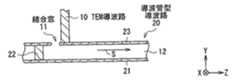
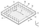
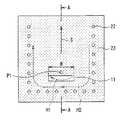
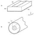
図1〜図3は、本発明の一実施の形態に係る高周波モジュールの第1の構成例を示している。図1は、図2および図3のAA線部分の断面に対応する。図3では、図面の簡略化のため、最上層の厚みを省略し、ハッチングを施している。この高周波モジュールは、TEMモードと他のモードとの変換構造を有しており、例えば高周波信号用の伝送路およびフィルタなどに使用することができる。この高周波モジュールは、TEMモードの電磁波を伝搬可能な導波路(以下、TEM導波路という。)10と、このTEM導波路10に結合され、TEMモードとは異なる他のモードの電磁波を伝搬する多層構造の導波管型導波路20とを備えている。この構成例において、TEM導波路10は、本発明における「第2の導波路」の一具体例に対応し、導波管型導波路20は、本発明における「第2の導波路」の一具体例に対応する。
【0024】
導波管型導波路20は、誘電体基板12を挟んで互いに対向するグランド電極21,23と、これらグランド電極21,23間を導通する導通体としての複数のスルーホール22とを有している。導波管型導波路20では、それらグランド電極21,23とスルーホール22とにより囲まれた領域内を、例えば図のS方向に電磁波が伝搬するようになっている。なお、導波管型導波路20は、その電磁波の伝搬領域が誘電体で満たされた誘電体導波管の構成であっても良いし、内部を空洞にしたキャビティ導波管の構成であっても良い。スルーホール22は、伝搬される電磁波が漏れ出さないよう、所定値以下(例えば信号波長の1/4以下)の間隔で設けられている。スルーホール22の内面は、メタライズされている。スルーホール22の断面形状は、円形に限らず、多角形または楕円等、他の形状であっても良い。
【0025】
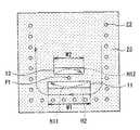
導波管型導波路20において、TEM導波路10との接続位置P1付近には、TEM導波路10との結合調整用の結合窓11が設けられている。図の例では、上側のグランド電極23に結合窓11を設け、TEM導波路10をその周辺に結合するようにしている。結合窓11は、グランド電極23を部分的に、例えば矩形状に切り欠いて形成されている。なお、結合窓11を下側のグランド電極21に設け、TEM導波路10を下側のグランド電極21側に結合するようにしても良い。また、接続位置P1を、結合窓11に対し図示した位置とは反対側(対称位置側)に設けるようにしても良い。すなわち、図の例では、結合窓11から見て接続位置P1が導波管型導波路20の内側寄りに設けられているが、結合窓11から見て外側(周辺側)寄りに設けられていても良い。
【0026】
TEM導波路10は、例えばマイクロストリップ線路、または同軸線路などの導波路であり、TEMモードの電磁波を伝搬可能であれば、特に限定されるものではない。TEM導波路10は、導波管型導波路20のグランド電極21,23の積層方向(Y方向)に延在し、その端部が、積層方向側から、ひとつのグランド電極23に直接的に接続され、導通されている。また、TEM導波路10は、導波管型導波路20のH面(磁界に平行な面)において磁界結合されている。なお、導波管型導波路20がTEモードで、電磁波の進行方向Sが図1のZ方向のとき、導波管型導波路20のH面は図のXZ平面に平行な面となる。
【0027】
この高周波モジュールにおいて、TEM導波路10と導波管型導波路20との接続部およびその近傍におけるH面内での磁界分布は、概略図3に示したようになる。TEM導波路10は、TEMモードであるからその磁界分布は、TEM導波路10の周囲に環状に分布している。しかし、接続部近傍においては、端部がグランド電極23に導通されているので、TEM導波路10の磁界H1は、主に接続部周辺に設けられた結合窓11付近に分布している。一方、導波管型導波路20の磁界H2は、例えば最低次のTEモード(TE10モード)であるものとすると、H面内においては管壁に沿って渦状に分布している。従って、導波管型導波路20のH面内において図示したように、TEM導波路10の結合窓11内での磁界H1の方向と、導波管型導波路20の磁界H2の方向とを一致させることにより、結合窓11の近傍で磁界結合がなされ、TEMモードからTEモードへの変換がなされる。
【0028】
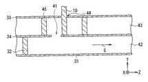
図6〜図8は、本発明の一実施の形態に係る高周波モジュールの第2の構成例を示している。図6は、図7および図8のBB線部分の断面に対応する。図7では、図面の簡略化のため、中間層の厚みを省略し、ハッチングを施している。この高周波モジュールは、図1〜図3に示した高周波モジュールと同様、TEMモードと他のモードとの変換構造を有している。この高周波モジュールが、図1〜図3に示した高周波モジュールと異なるのは、導波管型導波路30の部分である。この構成例では、導波管型導波路30が、本発明における「第2の導波路」の一具体例に対応する。
【0029】
導波管型導波路30は、2つの誘電体基板42,43と、これら誘電体基板42,43上に設けられた互いに対向する3層のグランド電極31,33,34と、これらグランド電極31,33,34の少なくとも2層間を導通する導通体としての複数のスルーホール32,45とを有している。下側グランド電極31は、下側の誘電体基板42の底面に一様に設けられている。上側グランド電極33は、上側の誘電体基板43の上面に一様に設けられている。中間グランド電極34は、誘電体基板42,43の間に設けられている。
【0030】
スルーホール32,45は、伝搬される電磁波が漏れ出さないよう、所定値以下(例えば信号波長の1/4以下)の間隔で設けられている。スルーホール32,45の内面は、メタライズされている。スルーホール32,45の断面形状は、円形に限らず、多角形または楕円等、他の形状であっても良い。スルーホール45は、上側グランド電極33と中間グランド電極34とを導通している。スルーホール32は、下側グランド電極31と中間グランド電極34とを導通している。スルーホール45は、TEM導波路10との接続位置P1の周囲を取り囲むように配置されている。
【0031】
この導波管型導波路30では、下側グランド電極31、中間グランド電極34およびスルーホール32により囲まれた領域内を、例えば図のS方向に電磁波が伝搬するようになっている。なお、導波管型導波路30は、その電磁波の伝搬領域が誘電体で満たされた誘電体導波管の構成であっても良いし、内部を空洞にしたキャビティ導波管の構成であっても良い。
【0032】
この構成例では、TEM導波路10は、導波管型導波路30のグランド電極31,33,34の積層方向(Y方向)に延在し、その端部が、上側グランド電極33を介して積層方向側から、中間グランド電極34に直接的に接続され、導通されるようになっている。このため、上側グランド電極33には、TEM導波路10が挿通される挿通孔44が設けられている。また、中間グランド電極34には、TEM導波路10との接続位置P1付近に結合調整用の結合窓41が設けられている。結合窓41は、中間グランド電極34を部分的に、例えば矩形状に切り欠いて形成されている。挿通孔44および結合窓41は、図8などから分かるようにスルーホール45に囲まれた領域内に設けられている。
【0033】
この構成例においても、TEM導波路10は、導波管型導波路30のH面において磁界結合されている。この高周波モジュールにおいて、TEM導波路10と導波管型導波路30との接続部およびその近傍におけるH面内での磁界分布は、概略図8に示したようになる。接続部近傍におけるTEM導波路10の磁界H1は、上述の第1の構成例と同様、主に接続部周辺に設けられた結合窓41付近に分布している。一方、導波管型導波路30の磁界H2は、例えば最低次のTEモード(TE10モード)であるものとすると、H面内においては管壁に沿って渦状に分布している。従って、導波管型導波路30のH面内において図示したように、TEM導波路10の結合窓41内での磁界H1の方向と、導波管型導波路30の磁界H2の方向とを一致させることにより、結合窓41の近傍で磁界結合がなされ、TEMモードからTEモードへの変換がなされる。
【0034】
このように、以上の各構成の高周波モジュールでは、第1の導波路としてのTEM導波路10に、TEMモードの電磁波が伝搬される。TEMモードの電磁波は、TEMモード以外のモードを伝搬する第2の導波路(導波管型導波路20,30)へと伝搬される。第1の導波路と第2の導波路との接続部分においては、図3および図8に示したように、第2の導波路のH面内において、第1の導波路に伝搬される電磁波の磁界H1の方向と第2の導波路に伝搬される電磁波の磁界H2の方向とが一致するように、磁界結合がなされ、これにより、TEMモードから他のモードへと変換がなされる。
【0035】
ここで、図1〜図3の第1の構成例を例に、磁界結合の度合いを調整する方法について説明する。
【0036】
まず、第1の調整方法として、結合窓11の幅W(図3)によって調整する方法がある。この場合、幅Wを短くすると、結合の度合いが弱くなるように作用する。
【0037】
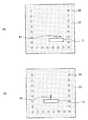
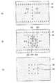
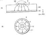
次に、第2の調整方法として、導波管型導波路20における磁界の強度分布を考慮し、TEM導波路10を接続する位置自体で調整する方法がある。図9(A),(B)に示したように、一般に多角形状の導波管(キャビティ共振器)では、多角形状の各辺の中央付近で磁界強度が最大になる。なお図9(A),(B)は、それぞれH面方向の断面形状が四角形状および三角形状の導波管における、H面内での磁界分布を示している。図中、ハッチングを施した領域が磁界強度が強い領域である。
【0038】
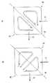
従って、図3に示したように、TEM導波路10を導波管型導波路20の辺(スルーホールによって22によって形成された側壁面)の中央付近で接続し、結合窓11もその周辺に設ければ、そこは磁界強度が強いので、結合の度合いが強くなる。一方、接続位置P1および結合窓11を、例えば図4(A),(B)における矢印方向へ移動させ、辺の中央から離れた位置で結合すれば、それだけ結合の度合いが弱くなる。図4(A)は、接続位置P1および結合窓11を、辺の端部に配置した例であり、(B)は、管路の中心部に配置した例である。
【0039】
次に、第3の調整方法として、図5に示したように、結合窓11とは異なる位置に別途結合調整用の調整窓13を設ける方法がある。調整窓13は、結合窓11と同様、グランド電極23を部分的に例えば矩形状に切り欠いて形成されている。調整窓13は、例えば接続位置P1を挟んで結合窓11とは反対側の位置に配置される。
【0040】
この場合、接続位置P1周辺においては、TEM導波路10による磁界は、主に結合窓11と調整窓13との付近に分布する。そして、それらの磁界H11,H12は、逆向きになる。従って、結合窓11における磁界H11の方向は、導波管型導波路20の磁界H2の方向と一致する。一方、調整窓13における磁界H12の方向は、磁界H2の方向と逆向きになり、結合が打ち消される方向に働く。このため、結合窓11の幅W1と調整窓13の幅W2とを調節することにより、結合調整を行うことができる。例えば、結合窓11の幅W1を一定のまま、調整窓13の幅W2を大きくしていくと、結合はしだいに弱くなる。
【0041】
なお、以上の説明では、電磁波が第1の導波路から第2の導波路側へと伝搬されるものとしていたが、これとは逆に、電磁波が第2の導波路から第1の導波路側へと伝搬されるようにしても良い。
【0042】
以上説明したように、本実施の形態によれば、第1の導波路の端部を、グランド電極の積層方向側から、直接的に第2の導波路のグランド電極のひとつに導通させ、かつ、第1の導波路と第2の導波路との磁界の方向を、H面内において一致させて磁界結合するようにしたので、各導波路間において、TEMモードとその他のモードとのモード変換を良好に行うことができる。
【0043】
また、本実施の形態によれぱ、第1の導波路を、グランド電極に直接または間接的に第2の導波路のグランド電極に導通させているので、その接続位置を変化させることなく、広い周波数帯域において最大効率での結合を行うことが可能である。
【0044】
このことを図10(A),(B)に示した比較例のモード変換構造を参照して説明する。図10(A)は、このモード変換構造の平面図、図10(B)は側面方向の構成を示している。このモード変換構造では、第2の導波路320におけるグランド電極321の一部に結合窓322が形成されている。この第2の導波路320に、端部が開放(オープン)端となっているマイクロストリップ線路などの第1の導波路310を最大効率で結合させることを考える。この場合、図に示したように、第1の導波路310の開放端からλ/4(λ;信号波長)の長さの所に結合窓322を位置させることで、結合の度合いが最大になる。しかし、このようなモード変換構造の場合、最大効率で結合させようとすると、信号周波数に応じて、第1の導波路310と結合窓322との位置関係を修正する必要がある。
【0045】
これに対し、本実施の形態のモード変換構造の場合、接続部分において、第1の導波路と第2の導波路とが直接導通されているので、信号周波数が変わったとしても、接続位置の調整をすることなく、常に最大効率で結合(モード変換)させることができる。すなわち、広帯域において最大効率での結合を行うことが可能となる。
【0046】
[変形例]
次に、以上の高周波モジュール、ならびにモード変換構造および方法の変形例について説明する。
【0047】
<第1の変形例>
図11は、本変形例における高周波モジュールの構成を示している。図12には、この高周波モジュールの平面図を示す。図11では、図面の簡略化のため、最上層の厚みを省略し、ハッチングを施している。本変形例は、第2の導波路を多重モード(2重モード)の導波管型導波路90とした構成例である。この構成例では、2重モードの導波管型導波路90の信号の入出力部に、TEM導波路10が接続されるようになっている。
【0048】
導波管型導波路90は、誘電体基板72と、互いに対向するグランド電極91,93と、これらグランド電極91,93間を導通する導通体としての複数のスルーホール92とを有し、それらグランド電極91,93とスルーホール92とにより囲まれた領域内を、例えば図のS1,S2方向に電磁波が2つのモードで伝搬するようになっている。スルーホール92は、全体として例えば略正方形状に配列されている。
【0049】
TEM導波路10と導波管型導波路90との接続構造は、基本的に、図1〜図3に示した第1の構成例と同様であり、導波管型導波路90において、TEM導波路10との接続位置P11,P12付近には、TEM導波路10との結合調整用の結合窓71,81が設けられている。図の例では、上側のグランド電極93に結合窓71,81を設け、TEM導波路10をその周辺に結合するようにしている。なお、結合窓71,81を下側のグランド電極91に設け、TEM導波路10を下側のグランド電極91側に結合するようにしても良い。
【0050】
本変形例においても、TEM導波路10は、導波管型導波路90のグランド電極91,93の積層方向(Y方向)に延在し、その端部が、積層方向側から、ひとつのグランド電極93に直接的に接続され、導通される。また、TEM導波路10は、導波管型導波路90のH面において磁界結合されている。本変形例では、例えば接続位置P11側に信号が入力され、接続位置P12側から信号が出力される。
【0051】
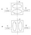
図13(A),(B)に、この導波管型導波路90の2つのモードにおける磁界分布を示す。この導波管型導波路90では、構造的な対称面96に対して平行に磁界分布が生じる第1のモード(図13(A))と、対称面96に対して垂直に磁界分布が生じる第2のモード(図13(B))とが存在する。また、この導波管型導波路90では、対称面96とは反対側の対角位置94,95において、電磁波の伝搬領域の形状を変えることにより、信号周波数の帯域を調整することができる。例えば、伝搬領域の形状を、図示したように角を削り取ったような形状にすることにより、帯域を広げることができる。
【0052】
なお、2重モードの導波路は、以上の構成以外にも種々のものがある。例えば、図14(A),(B)に示したような2つの磁界分布モードで励振するような導波路がある。この導波路においても、構造的な対称面97に対して平行に磁界分布が生じる第1のモード(図14(B))と、対称面96に対して垂直に磁界分布が生じる第2のモード(図14(A))とが存在する。このように他の構成の2重モードの導波路に対しても、本実施の形態のモード変換構造を適用することが可能である。
【0053】
このように、本変形例によれば、2重モードの導波管型導波路90に対してもTEMモードの導波路を接続し、TEMモードと他のモード間との変換を行うことができる。
【0054】
<第2の変形例>
図15〜図17は、本変形例における高周波モジュールの構成を示している。図15では、図面の簡略化のため、中間層の厚みを省略し、ハッチングを施している。図17は、図15におけるCC線部分の断面に対応する。
【0055】
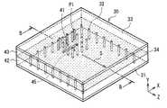
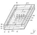
これまでの各構成例の高周波モジュールでは、第2の導波路側における電磁波の伝搬領域はひとつだけであったが、本変形例では、第2の導波路としての多層構造の導波管型導波路60が、電磁波の伝搬領域を複数有している。
【0056】
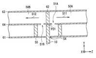
導波管型導波路60は、2つの誘電体基板52,53と、これら誘電体基板52,53上に設けられた互いに対向する3層のグランド電極61,63,64と、これらグランド電極61,63,64の少なくとも2層間を導通する導通体としての複数のスルーホール55,62とを有している。下側グランド電極61は、下側の誘電体基板52の底面に一様に設けられている。上側グランド電極63は、上側の誘電体基板53の上面に一様に設けられている。中間グランド電極64は、誘電体基板52,53の間に一様に設けられている。これら下側グランド電極61、中間グランド電極64、および上側グランド電極63の各層の平面構成を、それぞれ図16(A)〜(C)に示す。
【0057】
スルーホール55,62は、伝搬される電磁波が漏れ出さないよう、所定値以下(例えば信号波長の1/4以下)の間隔で設けられている。スルーホール55,62の内面は、メタライズされている。スルーホール55,62の断面形状は、円形に限らず、多角形または楕円等、他の形状であっても良い。スルーホール62は、上側グランド電極63と中間グランド電極64とを導通している。スルーホール55は、下側グランド電極61と中間グランド電極64とを導通している。スルーホール62は、上側グランド電極63と中間グランド電極64との間で、例えばH字状に配置されている。スルーホール55は、例えば、TEM導波路10との接続位置P21の周囲を取り囲むように配置されている。
【0058】
この導波管型導波路60では、上側グランド電極63、中間グランド電極64およびスルーホール62により囲まれた2つの伝搬領域50A,50B内を、異なる方向S11,S12に電磁波が伝搬するようになっている。なお、この導波管型導波路60は、その電磁波の伝搬領域50A,50Bが誘電体で満たされた誘電体導波管の構成であっても良いし、内部を空洞にしたキャビティ導波管の構成であっても良い。
【0059】
この構成例では、TEM導波路10は、導波管型導波路60のグランド電極61,63,64の積層方向(Y方向)に延在し、その端部が、下側グランド電極61を介して積層方向側から、中間グランド電極64に直接的に接続され、導通されるようになっている。このため、下側グランド電極61には、TEM導波路10が挿通される挿通孔54が設けられている。また、中間グランド電極64には、TEM導波路10との接続位置P21付近に結合調整用の結合窓51A,51Bが設けられている。結合窓51A,51Bは、中間グランド電極64を部分的に、例えば矩形状に切り欠いて形成されている。挿通孔54および結合窓51A,51Bは、スルーホール55に囲まれた領域内に設けられている。
【0060】
本変形例では、接続位置P21が、中間グランド電極64における2つの伝搬領域50A,50Bの境界部分に設定されている。また、結合窓51Aが、第1の伝搬領域50Aに対応する位置に設けられ、結合窓51Bが、第2の伝搬領域50Bに対応する位置に設けられている。これらの構造により、TEM導波路10が、2つの伝搬領域50A,50BのそれぞれのH面において磁界結合され、TEM導波路10を伝搬した電磁波が、2つの伝搬領域50A,50Bに分岐して伝搬されるようになっている。
【0061】
すなわち、図16(B)に示したように、接続位置P21周辺においては、TEM導波路10による磁界は、主に結合窓51A,51Bの付近に分布する。そして、それらの磁界H11,H12は、逆向きになる。ここで、接続部分において、導波管型導波路60の各伝搬領域50A,50Bにおける磁界H21,22の方向を、TEM導波路10の磁界H11,H12の方向と同じになるように設定すれば、各伝搬領域50A,50BのそれぞれのH面内において、良好に磁界結合がなされ、TEMモードから他のモードへの変換がなされる。
【0062】
本変形例によれば、TEMモードで伝搬されたひとつの高周波信号を、他のモードで複数に分岐して伝搬することができる。この変形例のモード変換構造は、デュプレクサなどに好適に用いることができる。
【0063】
なお、本発明は、以上の実施の形態に限定されず種々の変形実施が可能である。例えば、上記実施の形態では、第2の導波路(導波管型導波路)におけるグランド電極間を導通する構造として、スルーホールを用いた例を挙げたが、スルーホールとは異なる構造の導通体を用いるようにしても良い。例えば、スルーホールに代えて溝状の構造部分を設け、その内面をメタライズして金属壁とするような構成にしても良い。このような金属壁は、例えばマイクロマシン工法により作成することができる。
【0064】
【発明の効果】
以上説明したように、本発明の高周波モジュール、モード変換構造、または、モード変換方法によれば、第1の導波路の端部を、グランド電極の積層方向側から、直接的に第2の導波路のグランド電極のひとつに導通させ、かつ、第1の導波路と第2の導波路とを、第1の導波路に伝搬される電磁波の磁界の方向と第2の導波路に伝搬される電磁波の磁界の方向とが一致するように、第2の導波路のH面において磁界結合させるようにしたので、各導波路間において、TEMモードとその他のモードとのモード変換を良好に行うことができる。
【図面の簡単な説明】
【図1】本発明の一実施の形態に係る高周波モジュールの一構成例を示す断面図である。
【図2】図1に示した高周波モジュールの斜視図である。
【図3】図1に示した高周波モジュールの平面図である。
【図4】図1に示した高周波モジュールにおける結合調整の説明図である。
【図5】図1に示した高周波モジュールにおける結合調整の他の説明図である。
【図6】本発明の一実施の形態に係る高周波モジュールの他の構成例を示す断面図である。
【図7】図6に示した高周波モジュールの斜視図である。
【図8】図6に示した高周波モジュールにおける中間層の平面図である。
【図9】多角形状の導波管における磁界分布の例を示す説明図である。
【図10】本発明の一実施の形態に係る高周波モジュールに対する比較例を示す説明図である。
【図11】第1の変形例の高周波モジュールの構成を示す斜視図である。
【図12】図11に示した高周波モジュールの平面図である。
【図13】図11に示した高周波モジュールにおける磁界分布のモードを示す説明図である。
【図14】2重モードの他の例を示す説明図である。
【図15】第2の変形例の高周波モジュールの構成を示す斜視図である。
【図16】図15に示した高周波モジュールにおける各層の構成を示す平面図である。
【図17】図15に示した高周波モジュールの断面図である。
【図18】TEモードの導波管における電磁界分布の説明図である。
【図19】TEモードの導波管におけるE面内での電磁界分布を示す説明図である。
【図20】TMモードの導波管における電磁界分布の説明図である。
【図21】マイクロストリップ線路および同軸線路の構成図である。
【図22】マイクロストリップ線路および同軸線路におけるTEMモードの電磁界分布を示す説明図である。
【図23】従来のマイクロストリップ線路と導波管との接続構造の例を示す斜視図である。
【図24】図23に示した接続構造における電界分布を示す説明図である。
【符号の説明】
10…TEM導波路、11,41,51A,51B,71,81…結合窓、20,30,60,90…導波管型導波路、15,22,42…スルーホール。[0001]
TECHNICAL FIELD OF THE INVENTION
The present invention relates to a high-frequency module used for transmitting signals in a high-frequency band such as a microwave or a millimeter wave, and a mode conversion structure and a method for performing mode conversion between different waveguides.
[0002]
[Prior art]
2. Description of the Related Art Conventionally, strip lines, microstrip lines, coaxial lines, waveguides, dielectric waveguides, and the like have been known as transmission lines for transmitting high-frequency signals in a microwave band, a millimeter wave band, or the like. They are also known as constituting high frequency resonators and filters. In addition, MMICs (monolithic microwave integrated circuits) are examples of modularized components for these high frequencies. Hereinafter, a microstrip line, a waveguide, and the like that constitute a high-frequency transmission line and a filter are collectively referred to as a waveguide.
[0003]
Here, the propagation mode of the electromagnetic wave in the waveguide will be described. FIGS. 18A and 18B show a TE mode (TE mode) in a rectangular waveguide.10 (Mode), the electric field distribution (FIG. 2A) and the magnetic field distribution (FIG. 2B). 18A and 18B, the positions of the cross sections S1 to S5 correspond to each other. FIG. 19 shows an electromagnetic field distribution in the cross section S1. As shown in these figures, a state in which an electric field component exists only in the cross-sectional direction and no electric field component exists in the traveling direction (tube axis direction) Z of the electromagnetic wave is called a “TE mode”.
[0004]
FIGS. 20A and 20B show the TM mode (TM mode).11 Mode) in the state referred to as “mode”. FIG. 20A shows the electromagnetic field distribution in the XY section orthogonal to the tube axis direction Z, and FIG. 20B shows the electromagnetic field distribution in the YZ section on the side surface. As shown in these figures, a state in which a magnetic field component exists only in the cross-sectional direction and no magnetic field component exists in the traveling direction Z of the electromagnetic wave is called a “TM mode”.
[0005]
In each of these modes, a plane parallel to the electric field E is called an “E plane”, and a plane parallel to the magnetic field H is called an “H plane”. In the example of the TE mode in FIGS. 18A and 18B, a plane parallel to the XY plane is an E plane, and a plane parallel to the XZ plane is an H plane.
[0006]
On the other hand, in the microstrip line and the coaxial line shown in FIGS. 21A and 21B, a state called a TEM mode exists. Here, the microstrip line is, as shown in FIG. 21A, a ground (ground)
[0007]
FIGS. 22A and 22B show the electromagnetic field distribution in the TEM mode in the microstrip line and the coaxial line, respectively. As shown in these figures, a state in which both the electric field component and the magnetic field component exist only in the cross section and do not exist in the traveling direction Z of the electromagnetic wave is called a “TEM mode”.
[0008]
Incidentally, a high-frequency module having a plurality of waveguides requires a structure for interconnecting the respective waveguides. In particular, when connecting waveguides of different modes, a structure for performing mode conversion between the waveguides is required.
[0009]
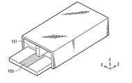
Conventionally, as a structure for connecting a microstrip line and a waveguide, for example, as shown in FIG. 23, a method of forming a so-called ridge waveguide in which a
[0010]
By the way, recently, there has been known one in which a dielectric waveguide line is formed by a lamination technique in a wiring board having a multilayer structure. This is provided with a plurality of ground conductors laminated with a dielectric interposed therebetween, and a through hole having an inner surface metallized and conducting between the ground conductors, and surrounded by the ground conductor and the through hole. The electromagnetic wave is propagated within. As a structure for connecting the waveguide having the multilayer structure to the microstrip line, for example, there is a structure described in
[0011]
As another structure for connecting different types of waveguides, there is an example in which an input / output terminal electrode is provided at the bottom end of the dielectric resonator, and this input / output terminal electrode is coupled to a line pattern on a printed circuit board ( Patent Document 2).
[0012]
[Patent Document 1]
JP 2000-216605 A
[Patent Document 2]
JP 2002-135003 A
[0013]
[Problems to be solved by the invention]
As described above, several structures for connecting different waveguides are conventionally known. On the other hand, a multilayer waveguide is a relatively recent technology, and a structure for connecting to a heterogeneous waveguide is known. , There are still areas where development is inadequate. In particular, when a TEM mode waveguide is connected to a multilayered waveguide, there is room for improvement in a conversion structure for appropriately performing mode conversion between them.
[0014]
The present invention has been made in view of such a problem, and an object of the present invention is to provide a high-frequency module capable of favorably performing mode conversion between a TEM mode and another mode between a plurality of waveguides, and a mode conversion structure and It is to provide a method.
[0015]
[Means for Solving the Problems]
A high-frequency module according to the present invention includes a first waveguide that propagates an electromagnetic wave in a TEM mode, and a second waveguide that is coupled to the first waveguide and propagates an electromagnetic wave in another mode different from the TEM mode. It has. The second waveguide has a region surrounded by at least two layers of ground electrodes opposing each other and a conductor that conducts between the at least two layers of ground electrodes, and the second waveguide is configured to allow electromagnetic waves to propagate through the region. Has been done. The first waveguide extends in the direction in which the ground electrodes are laminated, and its end is directly connected to one of the ground electrodes of the second waveguide from the lamination direction side. Further, the first waveguide and the second waveguide are aligned so that the direction of the magnetic field of the electromagnetic wave propagated to the first waveguide and the direction of the magnetic field of the electromagnetic wave propagated to the second waveguide match. At the H plane of the second waveguide.
[0016]
The mode conversion structure according to the present invention includes a first waveguide that propagates a TEM mode electromagnetic wave, and a second waveguide that is coupled to the first waveguide and propagates an electromagnetic wave of another mode different from the TEM mode. A mode conversion structure for performing mode conversion between different waveguides, wherein the second waveguide comprises at least two layers of ground electrodes facing each other, and a conductor that conducts between the at least two layers of ground electrodes. And an electromagnetic wave propagates in the region. The first waveguide extends in the laminating direction of the ground electrode, and the end portion extends from the laminating direction side. The first waveguide and the second waveguide are electrically connected directly to one of the ground electrodes of the second waveguide, and the direction of the magnetic field of the electromagnetic wave propagated through the first waveguide and the direction of the second Magnetic field of electromagnetic wave propagated through waveguide As the direction coincides, by being magnetically coupled in the H-plane of the second waveguide, in which mode conversion has been made.
[0017]
The mode conversion method according to the present invention includes a first waveguide that propagates an electromagnetic wave in a TEM mode, and a second waveguide that is coupled to the first waveguide and propagates an electromagnetic wave in another mode different from the TEM mode. Wherein the second waveguide has a region surrounded by at least two layers of ground electrodes facing each other and a conductor that conducts between the at least two layers of ground electrodes, and electromagnetic waves pass through the region. A mode conversion method for a structure configured to propagate, comprising: a first waveguide extending in a stacking direction of a ground electrode, and an end portion extending from a stacking direction side to a second waveguide. Of the electromagnetic wave propagated through the first waveguide and the second waveguide through the first waveguide and the second waveguide. So that the direction of the magnetic field of the electromagnetic wave matches By magnetically coupled in the H plane of the second waveguide, in which to perform the mode conversion.
[0018]
In the high-frequency module and the mode conversion structure and method according to the present invention, a TEM mode electromagnetic wave is propagated through the first waveguide. In the second waveguide, an electromagnetic wave of another mode different from the TEM mode is provided in a region surrounded by at least two layers of ground electrodes facing each other and a conductor that conducts between the at least two layers of ground electrodes. Propagated. The end of the first waveguide is directly connected to one of the ground electrodes of the second waveguide from the lamination direction side of the ground electrode. The first waveguide and the second waveguide are aligned so that the direction of the magnetic field of the electromagnetic wave propagated to the first waveguide and the direction of the magnetic field of the electromagnetic wave propagated to the second waveguide match. At the H plane of the second waveguide. As a result, mode conversion between the TEM mode and another mode is performed at the connection between the first waveguide and the second waveguide.
[0019]
In the high-frequency module according to the present invention, a configuration may be employed in which a ground electrode is provided with a partially cut-out window at the coupling portion between the first waveguide and the second waveguide.
[0020]
Further, in the high-frequency module according to the present invention, the second waveguide has a structure having a plurality of propagation regions for propagating electromagnetic waves in different directions, and the end of the first waveguide is formed by the second waveguide. May be configured to be magnetically coupled at the boundary between the plurality of propagation regions.
[0021]
In this case, the end of the first waveguide is connected to the second waveguide so that the electromagnetic wave propagated through the first waveguide is branched and propagated to a plurality of propagation regions in the second waveguide. A configuration in which a magnetic field is coupled at a boundary between a plurality of propagation regions may be employed.
[0022]
BEST MODE FOR CARRYING OUT THE INVENTION
Hereinafter, embodiments of the present invention will be described in detail with reference to the drawings.
[0023]
1 to 3 show a first configuration example of a high-frequency module according to an embodiment of the present invention. FIG. 1 corresponds to a cross section taken along line AA of FIGS. 2 and 3. In FIG. 3, the thickness of the uppermost layer is omitted and hatched for simplification of the drawing. This high-frequency module has a conversion structure between a TEM mode and another mode, and can be used, for example, as a transmission line and a filter for a high-frequency signal. The high-frequency module includes a waveguide (hereinafter, referred to as a TEM waveguide) 10 capable of transmitting an electromagnetic wave in a TEM mode, and a multilayer coupled to the
[0024]
The
[0025]
In the
[0026]
The
[0027]
In this high-frequency module, the magnetic field distribution in the H plane at the connection between the
[0028]
6 to 8 show a second configuration example of the high-frequency module according to one embodiment of the present invention. FIG. 6 corresponds to a cross section taken along line BB of FIGS. 7 and 8. In FIG. 7, the thickness of the intermediate layer is omitted and hatched for simplification of the drawing. This high-frequency module has a conversion structure between a TEM mode and another mode, similarly to the high-frequency module shown in FIGS. This high-frequency module is different from the high-frequency module shown in FIGS. 1 to 3 in the portion of the
[0029]
The
[0030]
The through holes 32 and 45 are provided at intervals of a predetermined value or less (for example, 1/4 or less of the signal wavelength) so that the transmitted electromagnetic wave does not leak. The inner surfaces of the through
[0031]
In the
[0032]
In this configuration example, the
[0033]
Also in this configuration example, the
[0034]
As described above, in the high-frequency module of each configuration described above, the TEM mode electromagnetic wave is propagated to the
[0035]
Here, a method of adjusting the degree of magnetic field coupling will be described with reference to the first configuration example of FIGS. 1 to 3 as an example.
[0036]
First, as a first adjustment method, there is a method of adjusting the width W of the coupling window 11 (FIG. 3). In this case, when the width W is reduced, the degree of the coupling is reduced.
[0037]
Next, as a second adjustment method, there is a method of adjusting the position at which the
[0038]
Accordingly, as shown in FIG. 3, the
[0039]
Next, as a third adjustment method, there is a method of separately providing an
[0040]
In this case, around the connection position P1, the magnetic field due to the
[0041]
In the above description, the electromagnetic wave is propagated from the first waveguide to the second waveguide. On the contrary, the electromagnetic wave is transmitted from the second waveguide to the first waveguide. It may be made to propagate to the side.
[0042]
As described above, according to the present embodiment, the end of the first waveguide is directly connected to one of the ground electrodes of the second waveguide from the lamination direction side of the ground electrode, and The direction of the magnetic field of the first waveguide and the direction of the magnetic field of the second waveguide are aligned in the H plane so that the magnetic field coupling is performed. Therefore, the mode conversion between the TEM mode and the other modes is performed between the waveguides. Can be performed favorably.
[0043]
Further, according to the present embodiment, since the first waveguide is directly or indirectly connected to the ground electrode of the second waveguide, the first waveguide is widened without changing the connection position. It is possible to perform coupling with maximum efficiency in the frequency band.
[0044]
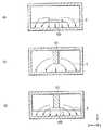
This will be described with reference to the mode conversion structure of the comparative example shown in FIGS. FIG. 10A is a plan view of this mode conversion structure, and FIG. 10B is a side view of the configuration. In this mode conversion structure, a
[0045]
On the other hand, in the case of the mode conversion structure of the present embodiment, since the first waveguide and the second waveguide are directly electrically connected at the connection portion, even if the signal frequency changes, the connection position is not changed. Coupling (mode conversion) can always be performed with maximum efficiency without adjustment. That is, it is possible to perform coupling with maximum efficiency in a wide band.
[0046]
[Modification]
Next, modifications of the above-described high-frequency module and mode conversion structure and method will be described.
[0047]
<First Modification>
FIG. 11 shows a configuration of a high-frequency module according to the present modification. FIG. 12 shows a plan view of this high-frequency module. In FIG. 11, the thickness of the uppermost layer is omitted and hatched for simplification of the drawing. This modification is a configuration example in which the second waveguide is a
[0048]
The
[0049]
The connection structure between the
[0050]
Also in this modified example, the
[0051]
FIGS. 13A and 13B show magnetic field distributions of the
[0052]
There are various types of dual mode waveguides other than the above-described configuration. For example, there is a waveguide that is excited in two magnetic field distribution modes as shown in FIGS. Also in this waveguide, a first mode in which a magnetic field distribution is generated parallel to the structural symmetry plane 97 (FIG. 14B) and a second mode in which a magnetic field distribution is generated perpendicular to the symmetry plane 96 (FIG. 14A). As described above, the mode conversion structure of the present embodiment can be applied to a dual-mode waveguide having another configuration.
[0053]
As described above, according to this modification, the TEM mode waveguide can be connected to the dual mode
[0054]
<Second Modification>
15 to 17 show the configuration of the high-frequency module according to the present modification. In FIG. 15, for simplification of the drawing, the thickness of the intermediate layer is omitted and hatched. FIG. 17 corresponds to a cross section taken along the line CC in FIG.
[0055]
In the high-frequency module of each configuration example so far, the electromagnetic wave propagation region on the second waveguide side is only one. However, in this modification, a multilayer waveguide type waveguide as the second waveguide is used. The wave path 60 has a plurality of electromagnetic wave propagation regions.
[0056]
The waveguide-type waveguide 60 includes two
[0057]
The through holes 55 and 62 are provided at intervals of a predetermined value or less (for example, 1/4 or less of the signal wavelength) so that the propagated electromagnetic wave does not leak. The inner surfaces of the through
[0058]
In the waveguide 60, electromagnetic waves propagate in different directions S11 and S12 in two
[0059]
In this configuration example, the
[0060]
In this modification, the connection position P21 is set at the boundary between the two
[0061]
That is, as shown in FIG. 16B, around the connection position P21, the magnetic field generated by the
[0062]
According to this modification, one high-frequency signal propagated in the TEM mode can be branched into a plurality of waves in another mode and propagated. The mode conversion structure of this modification can be suitably used for a duplexer or the like.
[0063]
Note that the present invention is not limited to the above embodiments, and various modifications can be made. For example, in the above-described embodiment, an example is described in which a through hole is used as a structure for conducting between ground electrodes in the second waveguide (waveguide type waveguide). A body may be used. For example, a structure in which a groove-shaped structural portion is provided instead of the through hole and the inner surface thereof is metallized to form a metal wall may be adopted. Such a metal wall can be created by, for example, a micromachine method.
[0064]
【The invention's effect】
As described above, according to the high-frequency module, the mode conversion structure, or the mode conversion method of the present invention, the end of the first waveguide is directly connected to the second conductor from the lamination direction side of the ground electrode. The first waveguide and the second waveguide are conducted to one of the ground electrodes of the waveguide, and the direction of the magnetic field of the electromagnetic wave propagated to the first waveguide is propagated to the second waveguide. Since the magnetic field is coupled on the H-plane of the second waveguide so that the direction of the magnetic field of the electromagnetic wave matches, the mode conversion between the TEM mode and the other modes can be performed well between the waveguides. Can be.
[Brief description of the drawings]
FIG. 1 is a cross-sectional view illustrating a configuration example of a high-frequency module according to an embodiment of the present invention.
FIG. 2 is a perspective view of the high-frequency module shown in FIG.
FIG. 3 is a plan view of the high-frequency module shown in FIG.
FIG. 4 is an explanatory diagram of coupling adjustment in the high-frequency module shown in FIG.
FIG. 5 is another explanatory diagram of the coupling adjustment in the high-frequency module shown in FIG. 1;
FIG. 6 is a cross-sectional view showing another configuration example of the high-frequency module according to one embodiment of the present invention.
FIG. 7 is a perspective view of the high-frequency module shown in FIG.
FIG. 8 is a plan view of an intermediate layer in the high-frequency module shown in FIG.
FIG. 9 is an explanatory diagram showing an example of a magnetic field distribution in a polygonal waveguide.
FIG. 10 is an explanatory diagram showing a comparative example with respect to the high-frequency module according to one embodiment of the present invention.
FIG. 11 is a perspective view illustrating a configuration of a high-frequency module according to a first modification.
FIG. 12 is a plan view of the high-frequency module shown in FIG.
FIG. 13 is an explanatory diagram showing modes of a magnetic field distribution in the high-frequency module shown in FIG.
FIG. 14 is an explanatory diagram showing another example of the dual mode.
FIG. 15 is a perspective view illustrating a configuration of a high-frequency module according to a second modification.
16 is a plan view showing a configuration of each layer in the high-frequency module shown in FIG.
FIG. 17 is a sectional view of the high-frequency module shown in FIG.
FIG. 18 is an explanatory diagram of an electromagnetic field distribution in a TE mode waveguide.
FIG. 19 is an explanatory diagram showing an electromagnetic field distribution in an E plane in a TE mode waveguide.
FIG. 20 is an explanatory diagram of an electromagnetic field distribution in a TM mode waveguide.
FIG. 21 is a configuration diagram of a microstrip line and a coaxial line.
FIG. 22 is an explanatory diagram showing a TEM mode electromagnetic field distribution in a microstrip line and a coaxial line.
FIG. 23 is a perspective view showing an example of a conventional connection structure between a microstrip line and a waveguide.
24 is an explanatory diagram showing an electric field distribution in the connection structure shown in FIG.
[Explanation of symbols]
10: TEM waveguide, 11, 41, 51A, 51B, 71, 81: coupling window, 20, 30, 60, 90: waveguide type waveguide, 15, 22, 42: through hole.
Claims (8)
Translated fromJapaneseこの第1の導波路に結合され、TEMモードとは異なる他のモードの電磁波を伝搬する第2の導波路と
を備え、
前記第2の導波路は、互いに対向する少なくとも2層のグランド電極と、少なくとも2層のグランド電極間を導通する導通体とにより囲まれた領域を有し、その領域内を電磁波が伝搬するようになされており、
前記第1の導波路が、前記グランド電極の積層方向に延在し、その端部が、前記積層方向側から、前記第2の導波路のグランド電極のひとつに直接導通され、かつ、前記第1の導波路と前記第2の導波路とが、前記第1の導波路に伝搬される電磁波の磁界の方向と前記第2の導波路に伝搬される電磁波の磁界の方向とが一致するように、前記第2の導波路のH面において磁界結合されている
ことを特徴とする高周波モジュール。A first waveguide for transmitting a TEM mode electromagnetic wave;
A second waveguide coupled to the first waveguide and transmitting an electromagnetic wave of another mode different from the TEM mode;
The second waveguide has a region surrounded by at least two layers of ground electrodes facing each other and a conductor that conducts between the at least two layers of ground electrodes, and an electromagnetic wave propagates in the region. Has been made,
The first waveguide extends in the stacking direction of the ground electrode, and an end thereof is directly connected to one of the ground electrodes of the second waveguide from the stacking direction side, and The first waveguide and the second waveguide are arranged such that the direction of the magnetic field of the electromagnetic wave propagated through the first waveguide matches the direction of the magnetic field of the electromagnetic wave propagated through the second waveguide. A high-frequency module, which is magnetically coupled on the H-plane of the second waveguide.
ことを特徴とする請求項1記載の高周波モジュール。The high-frequency module according to claim 1, wherein the second waveguide propagates a TE mode electromagnetic wave.
ことを特徴とする請求項1記載の高周波モジュール。2. The high-frequency module according to claim 1, wherein a window in which the electrode is partially cut out is provided in the ground electrode at a coupling portion between the first waveguide and the second waveguide. 3.
前記第1の導波路の端部が、前記第2の導波路における複数の伝搬領域の境界部分において磁界結合されている
ことを特徴とする請求項1記載の高周波モジュール。The second waveguide has a structure having a plurality of propagation regions that propagate electromagnetic waves in different directions,
2. The high-frequency module according to claim 1, wherein an end of the first waveguide is magnetically coupled at a boundary between a plurality of propagation regions in the second waveguide. 3.
ことを特徴とする請求項4記載の高周波モジュール。The end of the first waveguide is connected to the second waveguide so that the electromagnetic wave propagated through the first waveguide is branched and propagated to a plurality of propagation regions in the second waveguide. 5. The high-frequency module according to claim 4, wherein the magnetic field coupling is performed at the boundary between the plurality of propagation regions.
ことを特徴とする請求項1記載の高周波モジュール。The high-frequency module according to claim 1, wherein the second waveguide propagates an electromagnetic wave in multiple modes.
前記第2の導波路は、互いに対向する少なくとも2層のグランド電極と、少なくとも2層のグランド電極間を導通する導通体とにより囲まれた領域を有し、その領域内を電磁波が伝搬するようになされており、
前記第1の導波路が、前記グランド電極の積層方向に延在し、その端部が、前記積層方向側から、前記第2の導波路のグランド電極のひとつに直接導通され、かつ、前記第1の導波路と前記第2の導波路とが、前記第1の導波路に伝搬される電磁波の磁界の方向と前記第2の導波路に伝搬される電磁波の磁界の方向とが一致するように、前記第2の導波路のH面において磁界結合されていることにより、モード変換がなされている
ことを特徴とするモード変換構造。A first waveguide for transmitting an electromagnetic wave in a TEM mode, and a second waveguide coupled to the first waveguide for transmitting an electromagnetic wave in another mode different from the TEM mode. A mode conversion structure for performing conversion,
The second waveguide has a region surrounded by at least two layers of ground electrodes facing each other and a conductor that conducts between the at least two layers of ground electrodes, and an electromagnetic wave propagates in the region. Has been made,
The first waveguide extends in the stacking direction of the ground electrode, and an end thereof is directly connected to one of the ground electrodes of the second waveguide from the stacking direction side, and The first waveguide and the second waveguide are arranged such that the direction of the magnetic field of the electromagnetic wave propagated through the first waveguide matches the direction of the magnetic field of the electromagnetic wave propagated through the second waveguide. A mode conversion structure characterized in that mode conversion is performed by magnetic field coupling on the H-plane of the second waveguide.
前記第1の導波路を、前記グランド電極の積層方向に延在し、その端部を、前記積層方向側から、前記第2の導波路のグランド電極のひとつに直接導通し、
かつ、前記第1の導波路と前記第2の導波路とを、前記第1の導波路に伝搬される電磁波の磁界の方向と前記第2の導波路に伝搬される電磁波の磁界の方向とが一致するように、前記第2の導波路のH面において磁界結合することにより、モード変換を行う
ことを特徴とするモード変換方法。A first waveguide for transmitting an electromagnetic wave in a TEM mode, and a second waveguide coupled to the first waveguide for transmitting an electromagnetic wave in another mode different from the TEM mode; The waveguide has a region surrounded by at least two layers of ground electrodes facing each other and a conductor that conducts between the at least two layers of ground electrodes, and is configured such that electromagnetic waves propagate in the region. Mode conversion method for a structure having
The first waveguide extends in the direction of lamination of the ground electrode, and the end thereof is directly connected to one of the ground electrodes of the second waveguide from the lamination direction side,
Further, the direction of the magnetic field of the electromagnetic wave propagating in the first waveguide and the direction of the magnetic field of the electromagnetic wave propagating in the second waveguide are defined by the first waveguide and the second waveguide. Wherein the mode conversion is performed by performing magnetic field coupling on the H-plane of the second waveguide so that?
Priority Applications (4)
| Application Number | Priority Date | Filing Date | Title |
|---|---|---|---|
| JP2002313853AJP2004153367A (en) | 2002-10-29 | 2002-10-29 | High frequency module, and mode converting structure and method |
| US10/692,823US7199680B2 (en) | 2002-10-29 | 2003-10-27 | RF module using mode converting structure having short-circuiting waveguides and connecting windows |
| EP03024600AEP1416576A1 (en) | 2002-10-29 | 2003-10-28 | TEM mode converting structure and method |
| CNA2003101036089ACN1499668A (en) | 2002-10-29 | 2003-10-29 | High frequency module and module converting structure and method |
Applications Claiming Priority (1)
| Application Number | Priority Date | Filing Date | Title |
|---|---|---|---|
| JP2002313853AJP2004153367A (en) | 2002-10-29 | 2002-10-29 | High frequency module, and mode converting structure and method |
Publications (1)
| Publication Number | Publication Date |
|---|---|
| JP2004153367Atrue JP2004153367A (en) | 2004-05-27 |
Family
ID=32089492
Family Applications (1)
| Application Number | Title | Priority Date | Filing Date |
|---|---|---|---|
| JP2002313853APendingJP2004153367A (en) | 2002-10-29 | 2002-10-29 | High frequency module, and mode converting structure and method |
Country Status (4)
| Country | Link |
|---|---|
| US (1) | US7199680B2 (en) |
| EP (1) | EP1416576A1 (en) |
| JP (1) | JP2004153367A (en) |
| CN (1) | CN1499668A (en) |
Cited By (2)
| Publication number | Priority date | Publication date | Assignee | Title |
|---|---|---|---|---|
| JP2010177866A (en)* | 2009-01-28 | 2010-08-12 | Kyocera Corp | Waveguide type rat race circuit |
| JP2010177865A (en)* | 2009-01-28 | 2010-08-12 | Kyocera Corp | Waveguide type rat race circuit |
Families Citing this family (163)
| Publication number | Priority date | Publication date | Assignee | Title |
|---|---|---|---|---|
| JP3845394B2 (en)* | 2003-06-24 | 2006-11-15 | Tdk株式会社 | High frequency module |
| US7873329B2 (en)* | 2006-04-25 | 2011-01-18 | ThruVision Systems Limited | Transceiver having mixer/filter within receiving/transmitting cavity |
| JP4769753B2 (en)* | 2007-03-27 | 2011-09-07 | 富士通株式会社 | Superconducting filter device |
| JP5309209B2 (en)* | 2009-03-31 | 2013-10-09 | 京セラ株式会社 | Waveguide structure, and high-frequency module and radar apparatus including waveguide structure |
| US20130265734A1 (en)* | 2012-04-04 | 2013-10-10 | Texas Instruments Incorporated | Interchip communication using embedded dielectric and metal waveguides |
| US20130265733A1 (en)* | 2012-04-04 | 2013-10-10 | Texas Instruments Incorporated | Interchip communication using an embedded dielectric waveguide |
| US10009065B2 (en) | 2012-12-05 | 2018-06-26 | At&T Intellectual Property I, L.P. | Backhaul link for distributed antenna system |
| US9113347B2 (en) | 2012-12-05 | 2015-08-18 | At&T Intellectual Property I, Lp | Backhaul link for distributed antenna system |
| US9999038B2 (en) | 2013-05-31 | 2018-06-12 | At&T Intellectual Property I, L.P. | Remote distributed antenna system |
| US9525524B2 (en) | 2013-05-31 | 2016-12-20 | At&T Intellectual Property I, L.P. | Remote distributed antenna system |
| US8897697B1 (en) | 2013-11-06 | 2014-11-25 | At&T Intellectual Property I, Lp | Millimeter-wave surface-wave communications |
| US9209902B2 (en) | 2013-12-10 | 2015-12-08 | At&T Intellectual Property I, L.P. | Quasi-optical coupler |
| US9692101B2 (en) | 2014-08-26 | 2017-06-27 | At&T Intellectual Property I, L.P. | Guided wave couplers for coupling electromagnetic waves between a waveguide surface and a surface of a wire |
| US9768833B2 (en) | 2014-09-15 | 2017-09-19 | At&T Intellectual Property I, L.P. | Method and apparatus for sensing a condition in a transmission medium of electromagnetic waves |
| US10063280B2 (en) | 2014-09-17 | 2018-08-28 | At&T Intellectual Property I, L.P. | Monitoring and mitigating conditions in a communication network |
| US9615269B2 (en) | 2014-10-02 | 2017-04-04 | At&T Intellectual Property I, L.P. | Method and apparatus that provides fault tolerance in a communication network |
| US9685992B2 (en) | 2014-10-03 | 2017-06-20 | At&T Intellectual Property I, L.P. | Circuit panel network and methods thereof |
| US9503189B2 (en) | 2014-10-10 | 2016-11-22 | At&T Intellectual Property I, L.P. | Method and apparatus for arranging communication sessions in a communication system |
| US9973299B2 (en) | 2014-10-14 | 2018-05-15 | At&T Intellectual Property I, L.P. | Method and apparatus for adjusting a mode of communication in a communication network |
| US9762289B2 (en) | 2014-10-14 | 2017-09-12 | At&T Intellectual Property I, L.P. | Method and apparatus for transmitting or receiving signals in a transportation system |
| US9312919B1 (en) | 2014-10-21 | 2016-04-12 | At&T Intellectual Property I, Lp | Transmission device with impairment compensation and methods for use therewith |
| US9520945B2 (en) | 2014-10-21 | 2016-12-13 | At&T Intellectual Property I, L.P. | Apparatus for providing communication services and methods thereof |
| US9780834B2 (en) | 2014-10-21 | 2017-10-03 | At&T Intellectual Property I, L.P. | Method and apparatus for transmitting electromagnetic waves |
| US9627768B2 (en) | 2014-10-21 | 2017-04-18 | At&T Intellectual Property I, L.P. | Guided-wave transmission device with non-fundamental mode propagation and methods for use therewith |
| US9577306B2 (en) | 2014-10-21 | 2017-02-21 | At&T Intellectual Property I, L.P. | Guided-wave transmission device and methods for use therewith |
| US9653770B2 (en) | 2014-10-21 | 2017-05-16 | At&T Intellectual Property I, L.P. | Guided wave coupler, coupling module and methods for use therewith |
| US9769020B2 (en) | 2014-10-21 | 2017-09-19 | At&T Intellectual Property I, L.P. | Method and apparatus for responding to events affecting communications in a communication network |
| US10340573B2 (en) | 2016-10-26 | 2019-07-02 | At&T Intellectual Property I, L.P. | Launcher with cylindrical coupling device and methods for use therewith |
| US9461706B1 (en) | 2015-07-31 | 2016-10-04 | At&T Intellectual Property I, Lp | Method and apparatus for exchanging communication signals |
| US10009067B2 (en) | 2014-12-04 | 2018-06-26 | At&T Intellectual Property I, L.P. | Method and apparatus for configuring a communication interface |
| US9680670B2 (en) | 2014-11-20 | 2017-06-13 | At&T Intellectual Property I, L.P. | Transmission device with channel equalization and control and methods for use therewith |
| US9997819B2 (en) | 2015-06-09 | 2018-06-12 | At&T Intellectual Property I, L.P. | Transmission medium and method for facilitating propagation of electromagnetic waves via a core |
| US9544006B2 (en) | 2014-11-20 | 2017-01-10 | At&T Intellectual Property I, L.P. | Transmission device with mode division multiplexing and methods for use therewith |
| US9954287B2 (en) | 2014-11-20 | 2018-04-24 | At&T Intellectual Property I, L.P. | Apparatus for converting wireless signals and electromagnetic waves and methods thereof |
| US9800327B2 (en) | 2014-11-20 | 2017-10-24 | At&T Intellectual Property I, L.P. | Apparatus for controlling operations of a communication device and methods thereof |
| US10243784B2 (en) | 2014-11-20 | 2019-03-26 | At&T Intellectual Property I, L.P. | System for generating topology information and methods thereof |
| US9742462B2 (en) | 2014-12-04 | 2017-08-22 | At&T Intellectual Property I, L.P. | Transmission medium and communication interfaces and methods for use therewith |
| US9654173B2 (en) | 2014-11-20 | 2017-05-16 | At&T Intellectual Property I, L.P. | Apparatus for powering a communication device and methods thereof |
| US9660316B2 (en)* | 2014-12-01 | 2017-05-23 | Huawei Technologies Co., Ltd. | Millimeter wave dual-mode diplexer and method |
| US10144036B2 (en) | 2015-01-30 | 2018-12-04 | At&T Intellectual Property I, L.P. | Method and apparatus for mitigating interference affecting a propagation of electromagnetic waves guided by a transmission medium |
| US9876570B2 (en) | 2015-02-20 | 2018-01-23 | At&T Intellectual Property I, Lp | Guided-wave transmission device with non-fundamental mode propagation and methods for use therewith |
| US9749013B2 (en) | 2015-03-17 | 2017-08-29 | At&T Intellectual Property I, L.P. | Method and apparatus for reducing attenuation of electromagnetic waves guided by a transmission medium |
| US9705561B2 (en) | 2015-04-24 | 2017-07-11 | At&T Intellectual Property I, L.P. | Directional coupling device and methods for use therewith |
| US10224981B2 (en) | 2015-04-24 | 2019-03-05 | At&T Intellectual Property I, Lp | Passive electrical coupling device and methods for use therewith |
| US9948354B2 (en) | 2015-04-28 | 2018-04-17 | At&T Intellectual Property I, L.P. | Magnetic coupling device with reflective plate and methods for use therewith |
| US9793954B2 (en) | 2015-04-28 | 2017-10-17 | At&T Intellectual Property I, L.P. | Magnetic coupling device and methods for use therewith |
| US9871282B2 (en) | 2015-05-14 | 2018-01-16 | At&T Intellectual Property I, L.P. | At least one transmission medium having a dielectric surface that is covered at least in part by a second dielectric |
| US9748626B2 (en) | 2015-05-14 | 2017-08-29 | At&T Intellectual Property I, L.P. | Plurality of cables having different cross-sectional shapes which are bundled together to form a transmission medium |
| US9490869B1 (en) | 2015-05-14 | 2016-11-08 | At&T Intellectual Property I, L.P. | Transmission medium having multiple cores and methods for use therewith |
| US10650940B2 (en) | 2015-05-15 | 2020-05-12 | At&T Intellectual Property I, L.P. | Transmission medium having a conductive material and methods for use therewith |
| US9917341B2 (en) | 2015-05-27 | 2018-03-13 | At&T Intellectual Property I, L.P. | Apparatus and method for launching electromagnetic waves and for modifying radial dimensions of the propagating electromagnetic waves |
| US9866309B2 (en) | 2015-06-03 | 2018-01-09 | At&T Intellectual Property I, Lp | Host node device and methods for use therewith |
| US9912381B2 (en) | 2015-06-03 | 2018-03-06 | At&T Intellectual Property I, Lp | Network termination and methods for use therewith |
| US10103801B2 (en) | 2015-06-03 | 2018-10-16 | At&T Intellectual Property I, L.P. | Host node device and methods for use therewith |
| US10812174B2 (en) | 2015-06-03 | 2020-10-20 | At&T Intellectual Property I, L.P. | Client node device and methods for use therewith |
| US9913139B2 (en) | 2015-06-09 | 2018-03-06 | At&T Intellectual Property I, L.P. | Signal fingerprinting for authentication of communicating devices |
| US10142086B2 (en) | 2015-06-11 | 2018-11-27 | At&T Intellectual Property I, L.P. | Repeater and methods for use therewith |
| US9608692B2 (en) | 2015-06-11 | 2017-03-28 | At&T Intellectual Property I, L.P. | Repeater and methods for use therewith |
| US9820146B2 (en) | 2015-06-12 | 2017-11-14 | At&T Intellectual Property I, L.P. | Method and apparatus for authentication and identity management of communicating devices |
| US9667317B2 (en) | 2015-06-15 | 2017-05-30 | At&T Intellectual Property I, L.P. | Method and apparatus for providing security using network traffic adjustments |
| US9640850B2 (en) | 2015-06-25 | 2017-05-02 | At&T Intellectual Property I, L.P. | Methods and apparatus for inducing a non-fundamental wave mode on a transmission medium |
| US9865911B2 (en) | 2015-06-25 | 2018-01-09 | At&T Intellectual Property I, L.P. | Waveguide system for slot radiating first electromagnetic waves that are combined into a non-fundamental wave mode second electromagnetic wave on a transmission medium |
| US9509415B1 (en) | 2015-06-25 | 2016-11-29 | At&T Intellectual Property I, L.P. | Methods and apparatus for inducing a fundamental wave mode on a transmission medium |
| US9853342B2 (en) | 2015-07-14 | 2017-12-26 | At&T Intellectual Property I, L.P. | Dielectric transmission medium connector and methods for use therewith |
| US10044409B2 (en) | 2015-07-14 | 2018-08-07 | At&T Intellectual Property I, L.P. | Transmission medium and methods for use therewith |
| US9836957B2 (en) | 2015-07-14 | 2017-12-05 | At&T Intellectual Property I, L.P. | Method and apparatus for communicating with premises equipment |
| US10033108B2 (en) | 2015-07-14 | 2018-07-24 | At&T Intellectual Property I, L.P. | Apparatus and methods for generating an electromagnetic wave having a wave mode that mitigates interference |
| US10033107B2 (en) | 2015-07-14 | 2018-07-24 | At&T Intellectual Property I, L.P. | Method and apparatus for coupling an antenna to a device |
| US9722318B2 (en) | 2015-07-14 | 2017-08-01 | At&T Intellectual Property I, L.P. | Method and apparatus for coupling an antenna to a device |
| US10320586B2 (en) | 2015-07-14 | 2019-06-11 | At&T Intellectual Property I, L.P. | Apparatus and methods for generating non-interfering electromagnetic waves on an insulated transmission medium |
| US9847566B2 (en) | 2015-07-14 | 2017-12-19 | At&T Intellectual Property I, L.P. | Method and apparatus for adjusting a field of a signal to mitigate interference |
| US10170840B2 (en) | 2015-07-14 | 2019-01-01 | At&T Intellectual Property I, L.P. | Apparatus and methods for sending or receiving electromagnetic signals |
| US9628116B2 (en) | 2015-07-14 | 2017-04-18 | At&T Intellectual Property I, L.P. | Apparatus and methods for transmitting wireless signals |
| US9882257B2 (en) | 2015-07-14 | 2018-01-30 | At&T Intellectual Property I, L.P. | Method and apparatus for launching a wave mode that mitigates interference |
| US10341142B2 (en) | 2015-07-14 | 2019-07-02 | At&T Intellectual Property I, L.P. | Apparatus and methods for generating non-interfering electromagnetic waves on an uninsulated conductor |
| US10148016B2 (en) | 2015-07-14 | 2018-12-04 | At&T Intellectual Property I, L.P. | Apparatus and methods for communicating utilizing an antenna array |
| US10205655B2 (en) | 2015-07-14 | 2019-02-12 | At&T Intellectual Property I, L.P. | Apparatus and methods for communicating utilizing an antenna array and multiple communication paths |
| US10090606B2 (en) | 2015-07-15 | 2018-10-02 | At&T Intellectual Property I, L.P. | Antenna system with dielectric array and methods for use therewith |
| US9608740B2 (en) | 2015-07-15 | 2017-03-28 | At&T Intellectual Property I, L.P. | Method and apparatus for launching a wave mode that mitigates interference |
| US9793951B2 (en) | 2015-07-15 | 2017-10-17 | At&T Intellectual Property I, L.P. | Method and apparatus for launching a wave mode that mitigates interference |
| US10784670B2 (en) | 2015-07-23 | 2020-09-22 | At&T Intellectual Property I, L.P. | Antenna support for aligning an antenna |
| US9871283B2 (en) | 2015-07-23 | 2018-01-16 | At&T Intellectual Property I, Lp | Transmission medium having a dielectric core comprised of plural members connected by a ball and socket configuration |
| US9912027B2 (en) | 2015-07-23 | 2018-03-06 | At&T Intellectual Property I, L.P. | Method and apparatus for exchanging communication signals |
| US9948333B2 (en) | 2015-07-23 | 2018-04-17 | At&T Intellectual Property I, L.P. | Method and apparatus for wireless communications to mitigate interference |
| US9749053B2 (en) | 2015-07-23 | 2017-08-29 | At&T Intellectual Property I, L.P. | Node device, repeater and methods for use therewith |
| US10020587B2 (en) | 2015-07-31 | 2018-07-10 | At&T Intellectual Property I, L.P. | Radial antenna and methods for use therewith |
| US9735833B2 (en) | 2015-07-31 | 2017-08-15 | At&T Intellectual Property I, L.P. | Method and apparatus for communications management in a neighborhood network |
| US9967173B2 (en) | 2015-07-31 | 2018-05-08 | At&T Intellectual Property I, L.P. | Method and apparatus for authentication and identity management of communicating devices |
| US9904535B2 (en) | 2015-09-14 | 2018-02-27 | At&T Intellectual Property I, L.P. | Method and apparatus for distributing software |
| US10079661B2 (en) | 2015-09-16 | 2018-09-18 | At&T Intellectual Property I, L.P. | Method and apparatus for use with a radio distributed antenna system having a clock reference |
| US10009063B2 (en) | 2015-09-16 | 2018-06-26 | At&T Intellectual Property I, L.P. | Method and apparatus for use with a radio distributed antenna system having an out-of-band reference signal |
| US10009901B2 (en) | 2015-09-16 | 2018-06-26 | At&T Intellectual Property I, L.P. | Method, apparatus, and computer-readable storage medium for managing utilization of wireless resources between base stations |
| US10136434B2 (en) | 2015-09-16 | 2018-11-20 | At&T Intellectual Property I, L.P. | Method and apparatus for use with a radio distributed antenna system having an ultra-wideband control channel |
| US9769128B2 (en) | 2015-09-28 | 2017-09-19 | At&T Intellectual Property I, L.P. | Method and apparatus for encryption of communications over a network |
| US9729197B2 (en) | 2015-10-01 | 2017-08-08 | At&T Intellectual Property I, L.P. | Method and apparatus for communicating network management traffic over a network |
| US9882277B2 (en) | 2015-10-02 | 2018-01-30 | At&T Intellectual Property I, Lp | Communication device and antenna assembly with actuated gimbal mount |
| US9876264B2 (en) | 2015-10-02 | 2018-01-23 | At&T Intellectual Property I, Lp | Communication system, guided wave switch and methods for use therewith |
| US10355367B2 (en) | 2015-10-16 | 2019-07-16 | At&T Intellectual Property I, L.P. | Antenna structure for exchanging wireless signals |
| US10665942B2 (en) | 2015-10-16 | 2020-05-26 | At&T Intellectual Property I, L.P. | Method and apparatus for adjusting wireless communications |
| US9912419B1 (en) | 2016-08-24 | 2018-03-06 | At&T Intellectual Property I, L.P. | Method and apparatus for managing a fault in a distributed antenna system |
| US9860075B1 (en) | 2016-08-26 | 2018-01-02 | At&T Intellectual Property I, L.P. | Method and communication node for broadband distribution |
| US10291311B2 (en) | 2016-09-09 | 2019-05-14 | At&T Intellectual Property I, L.P. | Method and apparatus for mitigating a fault in a distributed antenna system |
| US11032819B2 (en) | 2016-09-15 | 2021-06-08 | At&T Intellectual Property I, L.P. | Method and apparatus for use with a radio distributed antenna system having a control channel reference signal |
| US10340600B2 (en) | 2016-10-18 | 2019-07-02 | At&T Intellectual Property I, L.P. | Apparatus and methods for launching guided waves via plural waveguide systems |
| US10135147B2 (en) | 2016-10-18 | 2018-11-20 | At&T Intellectual Property I, L.P. | Apparatus and methods for launching guided waves via an antenna |
| US10135146B2 (en) | 2016-10-18 | 2018-11-20 | At&T Intellectual Property I, L.P. | Apparatus and methods for launching guided waves via circuits |
| US10811767B2 (en) | 2016-10-21 | 2020-10-20 | At&T Intellectual Property I, L.P. | System and dielectric antenna with convex dielectric radome |
| US9876605B1 (en) | 2016-10-21 | 2018-01-23 | At&T Intellectual Property I, L.P. | Launcher and coupling system to support desired guided wave mode |
| US9991580B2 (en) | 2016-10-21 | 2018-06-05 | At&T Intellectual Property I, L.P. | Launcher and coupling system for guided wave mode cancellation |
| US10374316B2 (en) | 2016-10-21 | 2019-08-06 | At&T Intellectual Property I, L.P. | System and dielectric antenna with non-uniform dielectric |
| US10312567B2 (en) | 2016-10-26 | 2019-06-04 | At&T Intellectual Property I, L.P. | Launcher with planar strip antenna and methods for use therewith |
| US10224634B2 (en) | 2016-11-03 | 2019-03-05 | At&T Intellectual Property I, L.P. | Methods and apparatus for adjusting an operational characteristic of an antenna |
| US10498044B2 (en) | 2016-11-03 | 2019-12-03 | At&T Intellectual Property I, L.P. | Apparatus for configuring a surface of an antenna |
| US10291334B2 (en) | 2016-11-03 | 2019-05-14 | At&T Intellectual Property I, L.P. | System for detecting a fault in a communication system |
| US10225025B2 (en) | 2016-11-03 | 2019-03-05 | At&T Intellectual Property I, L.P. | Method and apparatus for detecting a fault in a communication system |
| US10535928B2 (en) | 2016-11-23 | 2020-01-14 | At&T Intellectual Property I, L.P. | Antenna system and methods for use therewith |
| US10340603B2 (en) | 2016-11-23 | 2019-07-02 | At&T Intellectual Property I, L.P. | Antenna system having shielded structural configurations for assembly |
| US10178445B2 (en) | 2016-11-23 | 2019-01-08 | At&T Intellectual Property I, L.P. | Methods, devices, and systems for load balancing between a plurality of waveguides |
| US10340601B2 (en) | 2016-11-23 | 2019-07-02 | At&T Intellectual Property I, L.P. | Multi-antenna system and methods for use therewith |
| US10090594B2 (en) | 2016-11-23 | 2018-10-02 | At&T Intellectual Property I, L.P. | Antenna system having structural configurations for assembly |
| US10361489B2 (en) | 2016-12-01 | 2019-07-23 | At&T Intellectual Property I, L.P. | Dielectric dish antenna system and methods for use therewith |
| US10305190B2 (en) | 2016-12-01 | 2019-05-28 | At&T Intellectual Property I, L.P. | Reflecting dielectric antenna system and methods for use therewith |
| US10637149B2 (en) | 2016-12-06 | 2020-04-28 | At&T Intellectual Property I, L.P. | Injection molded dielectric antenna and methods for use therewith |
| US10382976B2 (en) | 2016-12-06 | 2019-08-13 | At&T Intellectual Property I, L.P. | Method and apparatus for managing wireless communications based on communication paths and network device positions |
| US10727599B2 (en) | 2016-12-06 | 2020-07-28 | At&T Intellectual Property I, L.P. | Launcher with slot antenna and methods for use therewith |
| US10755542B2 (en) | 2016-12-06 | 2020-08-25 | At&T Intellectual Property I, L.P. | Method and apparatus for surveillance via guided wave communication |
| US10819035B2 (en) | 2016-12-06 | 2020-10-27 | At&T Intellectual Property I, L.P. | Launcher with helical antenna and methods for use therewith |
| US10020844B2 (en) | 2016-12-06 | 2018-07-10 | T&T Intellectual Property I, L.P. | Method and apparatus for broadcast communication via guided waves |
| US10439675B2 (en) | 2016-12-06 | 2019-10-08 | At&T Intellectual Property I, L.P. | Method and apparatus for repeating guided wave communication signals |
| US10694379B2 (en) | 2016-12-06 | 2020-06-23 | At&T Intellectual Property I, L.P. | Waveguide system with device-based authentication and methods for use therewith |
| US9927517B1 (en) | 2016-12-06 | 2018-03-27 | At&T Intellectual Property I, L.P. | Apparatus and methods for sensing rainfall |
| US10135145B2 (en) | 2016-12-06 | 2018-11-20 | At&T Intellectual Property I, L.P. | Apparatus and methods for generating an electromagnetic wave along a transmission medium |
| US10326494B2 (en) | 2016-12-06 | 2019-06-18 | At&T Intellectual Property I, L.P. | Apparatus for measurement de-embedding and methods for use therewith |
| US10547348B2 (en) | 2016-12-07 | 2020-01-28 | At&T Intellectual Property I, L.P. | Method and apparatus for switching transmission mediums in a communication system |
| US10139820B2 (en) | 2016-12-07 | 2018-11-27 | At&T Intellectual Property I, L.P. | Method and apparatus for deploying equipment of a communication system |
| US9893795B1 (en) | 2016-12-07 | 2018-02-13 | At&T Intellectual Property I, Lp | Method and repeater for broadband distribution |
| US10446936B2 (en) | 2016-12-07 | 2019-10-15 | At&T Intellectual Property I, L.P. | Multi-feed dielectric antenna system and methods for use therewith |
| US10168695B2 (en) | 2016-12-07 | 2019-01-01 | At&T Intellectual Property I, L.P. | Method and apparatus for controlling an unmanned aircraft |
| US10027397B2 (en) | 2016-12-07 | 2018-07-17 | At&T Intellectual Property I, L.P. | Distributed antenna system and methods for use therewith |
| US10243270B2 (en) | 2016-12-07 | 2019-03-26 | At&T Intellectual Property I, L.P. | Beam adaptive multi-feed dielectric antenna system and methods for use therewith |
| US10359749B2 (en) | 2016-12-07 | 2019-07-23 | At&T Intellectual Property I, L.P. | Method and apparatus for utilities management via guided wave communication |
| US10389029B2 (en) | 2016-12-07 | 2019-08-20 | At&T Intellectual Property I, L.P. | Multi-feed dielectric antenna system with core selection and methods for use therewith |
| US10326689B2 (en) | 2016-12-08 | 2019-06-18 | At&T Intellectual Property I, L.P. | Method and system for providing alternative communication paths |
| US10777873B2 (en) | 2016-12-08 | 2020-09-15 | At&T Intellectual Property I, L.P. | Method and apparatus for mounting network devices |
| US10916969B2 (en) | 2016-12-08 | 2021-02-09 | At&T Intellectual Property I, L.P. | Method and apparatus for providing power using an inductive coupling |
| US10938108B2 (en) | 2016-12-08 | 2021-03-02 | At&T Intellectual Property I, L.P. | Frequency selective multi-feed dielectric antenna system and methods for use therewith |
| US9911020B1 (en) | 2016-12-08 | 2018-03-06 | At&T Intellectual Property I, L.P. | Method and apparatus for tracking via a radio frequency identification device |
| US10069535B2 (en) | 2016-12-08 | 2018-09-04 | At&T Intellectual Property I, L.P. | Apparatus and methods for launching electromagnetic waves having a certain electric field structure |
| US10103422B2 (en) | 2016-12-08 | 2018-10-16 | At&T Intellectual Property I, L.P. | Method and apparatus for mounting network devices |
| US10530505B2 (en) | 2016-12-08 | 2020-01-07 | At&T Intellectual Property I, L.P. | Apparatus and methods for launching electromagnetic waves along a transmission medium |
| US10389037B2 (en) | 2016-12-08 | 2019-08-20 | At&T Intellectual Property I, L.P. | Apparatus and methods for selecting sections of an antenna array and use therewith |
| US10601494B2 (en) | 2016-12-08 | 2020-03-24 | At&T Intellectual Property I, L.P. | Dual-band communication device and method for use therewith |
| US9998870B1 (en) | 2016-12-08 | 2018-06-12 | At&T Intellectual Property I, L.P. | Method and apparatus for proximity sensing |
| US10411356B2 (en) | 2016-12-08 | 2019-09-10 | At&T Intellectual Property I, L.P. | Apparatus and methods for selectively targeting communication devices with an antenna array |
| US9838896B1 (en) | 2016-12-09 | 2017-12-05 | At&T Intellectual Property I, L.P. | Method and apparatus for assessing network coverage |
| US10340983B2 (en) | 2016-12-09 | 2019-07-02 | At&T Intellectual Property I, L.P. | Method and apparatus for surveying remote sites via guided wave communications |
| US10264586B2 (en) | 2016-12-09 | 2019-04-16 | At&T Mobility Ii Llc | Cloud-based packet controller and methods for use therewith |
| US9973940B1 (en) | 2017-02-27 | 2018-05-15 | At&T Intellectual Property I, L.P. | Apparatus and methods for dynamic impedance matching of a guided wave launcher |
| US10298293B2 (en) | 2017-03-13 | 2019-05-21 | At&T Intellectual Property I, L.P. | Apparatus of communication utilizing wireless network devices |
| AT521225A1 (en)* | 2018-05-09 | 2019-11-15 | Siemens Ag Oesterreich | Electronic device with a housing and an antenna arrangement |
| JP6767591B1 (en)* | 2019-06-10 | 2020-10-14 | 株式会社フジクラ | Mode converters, RF modules, and mobile terminals |
| IL292203B2 (en)* | 2019-10-17 | 2025-09-01 | Thruvision Ltd | High frequency detection method and apparatus |
| EP4270633A4 (en)* | 2020-12-25 | 2024-11-13 | Kyocera Corporation | PRINTED WIRING BOARD, STACKED RESONATOR AND STACKED FILTER |
Family Cites Families (14)
| Publication number | Priority date | Publication date | Assignee | Title |
|---|---|---|---|---|
| JPH0653711A (en) | 1992-07-28 | 1994-02-25 | Fukushima Nippon Denki Kk | Waveguide line |
| JP3493265B2 (en) | 1996-09-30 | 2004-02-03 | 京セラ株式会社 | Dielectric waveguide line and wiring board |
| JP3537626B2 (en) | 1997-04-22 | 2004-06-14 | 京セラ株式会社 | High frequency package |
| JP3366552B2 (en)* | 1997-04-22 | 2003-01-14 | 京セラ株式会社 | Dielectric waveguide line and multilayer wiring board including the same |
| WO1998054782A1 (en)* | 1997-05-26 | 1998-12-03 | Telefonaktiebolaget Lm Ericsson | Microwave transmission device |
| JPH1119170A (en) | 1997-07-07 | 1999-01-26 | Toto Ltd | Sauna system for bathroom |
| US6057747A (en)* | 1997-08-22 | 2000-05-02 | Kyocera Corporation | Dielectric waveguide line and its branch structure |
| US6002305A (en)* | 1997-09-25 | 1999-12-14 | Endgate Corporation | Transition between circuit transmission line and microwave waveguide |
| JPH11284409A (en) | 1998-03-27 | 1999-10-15 | Kyocera Corp | Waveguide type bandpass filter |
| US6580335B1 (en) | 1998-12-24 | 2003-06-17 | Kabushiki Kaisha Toyota Chuo Kenkyusho | Waveguide-transmission line transition having a slit and a matching element |
| JP3517143B2 (en) | 1999-01-21 | 2004-04-05 | 京セラ株式会社 | Connection structure between dielectric waveguide line and high-frequency line conductor |
| JP3517148B2 (en) | 1999-03-01 | 2004-04-05 | 京セラ株式会社 | Connection structure between dielectric waveguide line and high-frequency line conductor |
| JP2002135003A (en) | 2000-10-27 | 2002-05-10 | Toko Inc | Waveguide type dielectric filter |
| JP3902072B2 (en) | 2001-07-17 | 2007-04-04 | 東光株式会社 | Dielectric waveguide filter and its mounting structure |
- 2002
- 2002-10-29JPJP2002313853Apatent/JP2004153367A/enactivePending
- 2003
- 2003-10-27USUS10/692,823patent/US7199680B2/ennot_activeExpired - Lifetime
- 2003-10-28EPEP03024600Apatent/EP1416576A1/ennot_activeWithdrawn
- 2003-10-29CNCNA2003101036089Apatent/CN1499668A/enactivePending
Cited By (2)
| Publication number | Priority date | Publication date | Assignee | Title |
|---|---|---|---|---|
| JP2010177866A (en)* | 2009-01-28 | 2010-08-12 | Kyocera Corp | Waveguide type rat race circuit |
| JP2010177865A (en)* | 2009-01-28 | 2010-08-12 | Kyocera Corp | Waveguide type rat race circuit |
Also Published As
| Publication number | Publication date |
|---|---|
| US20040085153A1 (en) | 2004-05-06 |
| CN1499668A (en) | 2004-05-26 |
| EP1416576A1 (en) | 2004-05-06 |
| US7199680B2 (en) | 2007-04-03 |
Similar Documents
| Publication | Publication Date | Title |
|---|---|---|
| JP2004153367A (en) | High frequency module, and mode converting structure and method | |
| JP3891918B2 (en) | High frequency module | |
| JP4568235B2 (en) | Transmission line converter | |
| JP3839410B2 (en) | Filter and resonator arrangement method | |
| JP2001196817A (en) | Dielectric resonator, dielectric filter, dielectric duplexer and communication apparatus | |
| JP2005260570A (en) | Microstrip line waveguide converter | |
| JP2005051331A (en) | Coupling structure of microstrip line and dielectric waveguide | |
| US20090021324A1 (en) | RF module | |
| JP2991076B2 (en) | Planar dielectric line and integrated circuit | |
| JP3891996B2 (en) | Waveguide type waveguide and high frequency module | |
| US7403085B2 (en) | RF module | |
| JP3013798B2 (en) | Crossing track | |
| JP2005051330A (en) | Connection structure between dielectric waveguide line and high-frequency transmission line, high-frequency circuit board using the same, and package for mounting high-frequency element | |
| CN114128037A (en) | Coupling member, microwave device, and electronic apparatus | |
| JP6276448B1 (en) | Diplexer | |
| US11228077B2 (en) | Microstrip DC block | |
| WO2005020367A1 (en) | Planar dielectric line, high-frequency active circuit, and transmitting/receiving device | |
| CN114335953A (en) | Transition structure and application thereof, and dual-mode resonant waveguide excitation method | |
| US20250253510A1 (en) | Mode conversion device | |
| JP2000174515A (en) | Coplanar waveguide-waveguide converter | |
| JP7699730B2 (en) | Multilayer substrate and antenna device using same | |
| JP7561015B2 (en) | Waveguide structure and horn antenna | |
| JP2023168665A (en) | High frequency circuit and radar device | |
| JP2002076725A (en) | Waveguide conversion structure |
Legal Events
| Date | Code | Title | Description |
|---|---|---|---|
| A621 | Written request for application examination | Free format text:JAPANESE INTERMEDIATE CODE: A621 Effective date:20041116 | |
| A977 | Report on retrieval | Free format text:JAPANESE INTERMEDIATE CODE: A971007 Effective date:20060227 | |
| A131 | Notification of reasons for refusal | Free format text:JAPANESE INTERMEDIATE CODE: A131 Effective date:20060620 | |
| A521 | Written amendment | Free format text:JAPANESE INTERMEDIATE CODE: A821 Effective date:20060815 Free format text:JAPANESE INTERMEDIATE CODE: A523 Effective date:20060815 | |
| A131 | Notification of reasons for refusal | Free format text:JAPANESE INTERMEDIATE CODE: A131 Effective date:20061019 | |
| A02 | Decision of refusal | Free format text:JAPANESE INTERMEDIATE CODE: A02 Effective date:20070226 |