JP2004153241A - Semiconductor light emitting device and method of manufacturing the same - Google Patents
Semiconductor light emitting device and method of manufacturing the sameDownload PDFInfo
- Publication number
- JP2004153241A JP2004153241AJP2003292127AJP2003292127AJP2004153241AJP 2004153241 AJP2004153241 AJP 2004153241AJP 2003292127 AJP2003292127 AJP 2003292127AJP 2003292127 AJP2003292127 AJP 2003292127AJP 2004153241 AJP2004153241 AJP 2004153241A
- Authority
- JP
- Japan
- Prior art keywords
- layer
- light emitting
- type
- semiconductor
- emitting device
- Prior art date
- Legal status (The legal status is an assumption and is not a legal conclusion. Google has not performed a legal analysis and makes no representation as to the accuracy of the status listed.)
- Pending
Links
Images


Classifications
- H—ELECTRICITY
- H10—SEMICONDUCTOR DEVICES; ELECTRIC SOLID-STATE DEVICES NOT OTHERWISE PROVIDED FOR
- H10H—INORGANIC LIGHT-EMITTING SEMICONDUCTOR DEVICES HAVING POTENTIAL BARRIERS
- H10H20/00—Individual inorganic light-emitting semiconductor devices having potential barriers, e.g. light-emitting diodes [LED]
- H10H20/80—Constructional details
- H10H20/83—Electrodes
- H10H20/831—Electrodes characterised by their shape
- H—ELECTRICITY
- H10—SEMICONDUCTOR DEVICES; ELECTRIC SOLID-STATE DEVICES NOT OTHERWISE PROVIDED FOR
- H10H—INORGANIC LIGHT-EMITTING SEMICONDUCTOR DEVICES HAVING POTENTIAL BARRIERS
- H10H20/00—Individual inorganic light-emitting semiconductor devices having potential barriers, e.g. light-emitting diodes [LED]
- H10H20/01—Manufacture or treatment
- H10H20/011—Manufacture or treatment of bodies, e.g. forming semiconductor layers
- H10H20/018—Bonding of wafers
- H—ELECTRICITY
- H10—SEMICONDUCTOR DEVICES; ELECTRIC SOLID-STATE DEVICES NOT OTHERWISE PROVIDED FOR
- H10H—INORGANIC LIGHT-EMITTING SEMICONDUCTOR DEVICES HAVING POTENTIAL BARRIERS
- H10H20/00—Individual inorganic light-emitting semiconductor devices having potential barriers, e.g. light-emitting diodes [LED]
- H10H20/01—Manufacture or treatment
- H10H20/032—Manufacture or treatment of electrodes
Landscapes
- Led Devices (AREA)
- Electrodes Of Semiconductors (AREA)
Abstract
Translated fromJapaneseDescription
Translated fromJapaneseこの発明は半導体発光素子及びその製造方法に関する。 The present invention relates to a semiconductor light emitting device and a method for manufacturing the same.
近年、半導体発光素子の中で光通信や発光ダイオード情報表示パネル等に発光ダイオード(LED)が広く用いられている。これらの発光ダイオードは高輝度であることが重要であるが、発光ダイオードの輝度、言い換えれば外部量子効率は、内部量子効率と光取り出し効率によってきまる。このうち光取り出し効率は素子構造に大きく影響される。 In recent years, among semiconductor light emitting devices, light emitting diodes (LEDs) have been widely used for optical communication, light emitting diode information display panels, and the like. It is important that these light emitting diodes have high luminance, but the luminance of the light emitting diodes, in other words, the external quantum efficiency is determined by the internal quantum efficiency and the light extraction efficiency. The light extraction efficiency is greatly affected by the element structure.
発光ダイオードでは発光波長に対して透明な基板を用いることが光取り出し効率を向上させることを目的として行われている。発光波長に対して不透明な基板を用いた場合には上面への出射光しか取り出せないのに対し、発光波長に対して透明な基板を用いた場合には上面だけでなく4つの側面からも光を取り出すことができるからである。また、下面における反射光も上面および側面から出射させることが可能となる。この方法はInGaAsP系の半導体材料を用いた赤外発光ダイオード、AlGaAs系の半導体材料を用いた赤色、赤外発光ダイオード、GaAsP系の半導体材料を用いた黄色発光ダイオード、GaP系の半導体材料を用いた緑色発光ダイオード等に適用されている。 In the light emitting diode, a substrate transparent to the emission wavelength is used for the purpose of improving light extraction efficiency. When a substrate that is opaque to the emission wavelength is used, only the emitted light to the top surface can be extracted, whereas when a substrate that is transparent to the emission wavelength is used, light is emitted not only from the top surface but also from the four side surfaces. Because it can be taken out. Further, the reflected light on the lower surface can be emitted from the upper surface and the side surface. This method uses an infrared light emitting diode using an InGaAsP-based semiconductor material, a red and infrared light emitting diode using an AlGaAs-based semiconductor material, a yellow light-emitting diode using a GaAsP-based semiconductor material, and a GaP-based semiconductor material. Green light-emitting diodes.
AlGaInP系の発光ダイオードであって発光波長に対して透明な基板を備えたものを作製する製造方法としては、図10(a)に示すように、発光波長に対して不透明なn型GaAs基板110上に、n型半導体層112、発光層114、p型半導体層116をエピタキシャル成長した後、この上に発光波長に対して透明なp型GaP基板120を接触させて熱処理を施すことによってp型半導体層116と直接接合し、しかる後、図10(b)に示すように、上記n型GaAs基板110を除去するという方法が知られている(例えば、特許文献1(特許第3230638号明細書)参照。)。 As a manufacturing method for manufacturing an AlGaInP-based light emitting diode having a substrate transparent to the emission wavelength, as shown in FIG. 10A, an n-
また、別の製造方法として、図11(a)に示すように、発光波長に対して不透明なn型GaAs基板210上に、n型半導体層212、発光層214、p型半導体層216および厚さ50μm〜100μm程度のp型GaP電流拡散層218をエピタキシャル成長し、続いて図11(b)に示すように、上記n型GaAs基板210を除去した後、図11(c)に示すように、その除去によって露出した面にp型GaP基板220を接触させて熱処理を施すことによってn型半導体層212と直接接合するという方法が知られている(例えば、特許文献2(特開平6−302857号公報)参照。)。なお、p型GaP電流拡散層218の厚さは50μm以下であるとウエハを取り扱う時に割れやすく、100μm以上であると成長時間が長くなり発光ダイオードのコストが高くなる。よって、成長時間とGaAs基板を除去した後のウエハの機械的強度との兼ね合いから、50μm〜100μm程度に設定されている。 As another manufacturing method, as shown in FIG. 11A, an n-
さらに、別の製造方法として、図12(a)に示すように、発光波長に対して不透明なn型GaAs基板310上に、p型GaAsバッファ層311、p型AlGaAs電流拡散層312、p型クラッド層313、活性層314、n型クラッド層、n型中間層316、n型GaP層317をエピタキシャル成長し、続いて図12(b)に示すように、その上にn型GaP基板318を形成し、しかる後、上記n型GaAs基板310を除去するという方法が知られている(例えば、特許文献3(特開2000−196139号公報)参照。)。 Further, as another manufacturing method, as shown in FIG. 12A, a p-type
しかし、上述の方法では、発光層(または活性層)の近傍のp型基板120,220やp型電流拡散層218,312中に含まれたZn、Mg等のp型ドーパントの総量が多いため、結晶成長または直接接合時の熱履歴によりp型ドーパントが発光層(または活性層)に拡散して、内部量子効率が低下し、素子の輝度が低下するという問題がある。特に、GaAs基板に格子整合し、かつ小さい抵抗率を実現可能なAlGaInP系発光ダイオードでは、発光波長に対して透明な唯一の公知材料であるAlxGa1-xAs(0.5≦x≦1)が用いられるが、このAlxGa1-xAs(0.5≦x≦1)内においてZn、Mg等の拡散係数が大きいため、問題が深刻になる。However, in the above-described method, the total amount of p-type dopants such as Zn and Mg contained in the p-
また、上記p型電流拡散層218,312は、他の層が数μm以下の厚さに成長されるのに対して、既述のように通常は数10μm以上の厚さに成長されるため、成長装置のメンテナンス頻度が多くなり、生産性が低下するという問題がある。メンテナンス作業時は有毒ガスが発生するため、安全性の観点からも、メンテナンス頻度は少ない方が好ましい。
そこで、この発明の課題は、発光層(または活性層)へのp型ドーパントの拡散を抑制して高輝度を実現でき、また、成長装置のメンテナンス頻度を少なくできる半導体発光素子及びその製造方法を提供することにある。 Accordingly, an object of the present invention is to provide a semiconductor light emitting device and a method of manufacturing the same, which can realize high luminance by suppressing diffusion of a p-type dopant into a light emitting layer (or an active layer) and can reduce maintenance frequency of a growth apparatus. To provide.
上記課題を解決するため、この発明の半導体発光素子の製造方法は、
ノンドープ型、弱いp型またはn型の第1の半導体基板上に単層または複数層の半導体からなる発光層を積層する工程と、
その発光層上に単層または複数層からなるn型の半導体層を積層する工程と、
上記n型の半導体層の表面に上記発光層の発光波長に対して透明な第2の半導体基板を形成する工程と、
その後上記第1の半導体基板を除去する工程と、
上記第1の半導体基板の除去によって露出した面に上記発光層の発光波長に対して透明な透光性電極層を形成する工程を有することを特徴とする。In order to solve the above problems, a method for manufacturing a semiconductor light emitting device of the present invention includes:
Stacking a light-emitting layer made of a single layer or a plurality of semiconductors on a non-doped, weak p-type or n-type first semiconductor substrate;
Stacking an n-type semiconductor layer consisting of a single layer or a plurality of layers on the light emitting layer;
Forming a second semiconductor substrate transparent to the emission wavelength of the light emitting layer on the surface of the n-type semiconductor layer;
Then removing the first semiconductor substrate;
Forming a light-transmitting electrode layer that is transparent to the emission wavelength of the light-emitting layer on the surface exposed by removing the first semiconductor substrate.
なお、第1の半導体基板の「弱いp型」とは、発光層(または活性層)へのp型ドーパントの拡散を実質的に無視できる程度のp型を意味する。 Note that the term “weak p-type” of the first semiconductor substrate means a p-type in which diffusion of the p-type dopant into the light emitting layer (or the active layer) can be substantially ignored.
この発明の半導体発光素子の製造方法によれば、発光層の上下に、それぞれこの発光層の発光波長に対して透明な透光性電極層、第2の半導体基板を備えた半導体発光素子が作製される。したがって、素子の上面および側面から外部へ光を取り出すことができ、発光波長に対して不透明な基板を用いた場合に比して光取り出し効率が高まる。また、発光層の近傍にp型基板やp型電流拡散層を設けないので、高温処理時のp型ドーパントの発光層への拡散が抑制される。しかも、第1の半導体基板の除去によって露出した面に透光性電極層を形成しているので、動作時に、通電電流がこの透光性電極層によって拡散されて、発光層へ均一に電流が注入される。したがって、内部量子効率が高まる。これらの結果、半導体発光素子の特性が向上して、高輝度が実現される。また、この発明の半導体発光素子の製造方法では、電流拡散層を設けないので、エピタキシャル成長させる層厚を低減できる。したがって、成長装置のメンテナンス頻度を少なくでき、生産性を高めるとともに安全性を向上させることができる。 According to the method for manufacturing a semiconductor light-emitting device of the present invention, a semiconductor light-emitting device including a light-transmitting electrode layer transparent to the emission wavelength of the light-emitting layer and a second semiconductor substrate above and below the light-emitting layer is manufactured. Is done. Therefore, light can be extracted to the outside from the top and side surfaces of the element, and the light extraction efficiency is increased as compared with the case where a substrate opaque to the emission wavelength is used. Further, since no p-type substrate or p-type current diffusion layer is provided near the light-emitting layer, diffusion of the p-type dopant into the light-emitting layer during high-temperature treatment is suppressed. Moreover, since the light-transmitting electrode layer is formed on the surface exposed by removing the first semiconductor substrate, the current is diffused by the light-transmitting electrode layer during operation, and the current is uniformly supplied to the light-emitting layer. Injected. Therefore, the internal quantum efficiency increases. As a result, the characteristics of the semiconductor light emitting element are improved, and high luminance is realized. Further, in the method for manufacturing a semiconductor light emitting device of the present invention, since the current diffusion layer is not provided, the layer thickness for epitaxial growth can be reduced. Therefore, the maintenance frequency of the growth apparatus can be reduced, and the productivity can be improved and the safety can be improved.
一実施形態の半導体発光素子の製造方法は、上記発光層を積層する工程の前に、上記第1の半導体基板上に、この第1の半導体基板上とは組成が異なる単層または複数層からなるp型の半導体層を形成する工程を有することを特徴とする。 In one embodiment of the present invention, the method for manufacturing a semiconductor light-emitting element includes, before the step of laminating the light-emitting layer, on the first semiconductor substrate, from a single layer or a plurality of layers having a composition different from that of the first semiconductor substrate. Forming a p-type semiconductor layer.
詳しくは、この一実施形態の半導体発光素子の製造方法は、
ノンドープ型、弱いp型またはn型の第1の半導体基板上に、この第1の半導体基板上とは組成が異なる単層または複数層からなるp型の半導体層を形成する工程と、
そのp型の半導体層上に単層または複数層の半導体からなる発光層を積層する工程と、
その発光層上に単層または複数層からなるn型の半導体層を積層する工程と、
上記n型の半導体層の表面に上記発光層の発光波長に対して透明な第2の半導体基板を形成する工程と、
その後上記第1の半導体基板を除去する工程と、
上記第1の半導体基板の除去によって露出した面に上記発光層の発光波長に対して透明な透光性電極層を形成する工程を有することを特徴とする。Specifically, the method for manufacturing the semiconductor light emitting device of the embodiment is as follows.
Forming, on a non-doped, weak p-type or n-type first semiconductor substrate, a p-type semiconductor layer composed of a single layer or a plurality of layers different in composition from the first semiconductor substrate;
Stacking a light-emitting layer made of a single layer or a plurality of semiconductors on the p-type semiconductor layer;
Stacking an n-type semiconductor layer consisting of a single layer or a plurality of layers on the light emitting layer;
Forming a second semiconductor substrate transparent to the emission wavelength of the light emitting layer on the surface of the n-type semiconductor layer;
Then removing the first semiconductor substrate;
Forming a light-transmitting electrode layer that is transparent to the emission wavelength of the light-emitting layer on the surface exposed by removing the first semiconductor substrate.
この一実施形態の半導体発光素子の製造方法によれば、発光層の上下に、それぞれこの発光層の発光波長に対して透明な透光性電極層、第2の半導体基板を備えた半導体発光素子が作製される。したがって、素子の上面および側面から外部へ光を取り出すことができ、発光波長に対して不透明な基板を用いた場合に比して光取り出し効率が高まる。また、発光層の近傍にp型基板を設けないので、高温処理時のp型ドーパントの発光層への拡散が抑制される。しかも、第1の半導体基板の除去によって露出した面に透光性電極層を形成しているので、動作時に、通電電流がこの透光性電極層によって拡散されて、発光層へ均一に電流が注入される。したがって、内部量子効率が高まる。さらに、透光性電極を形成する面が第1の半導体基板の除去によって露出した面、つまり単層または複数層からなるp型の半導体層の面であるから、上記発光層上に直接透光性電極を形成する場合に比して電極/半導体界面での電圧降下を小さくすることができる。これらの結果、半導体発光素子の特性が向上して、高輝度が実現される。また、この発明の半導体発光素子の製造方法では、電流拡散層を設けないので、エピタキシャル成長させる層厚を低減できる。したがって、成長装置のメンテナンス頻度を少なくでき、生産性を高めるとともに安全性を向上させることができる。 According to the method for manufacturing a semiconductor light emitting device of this embodiment, a semiconductor light emitting device including a transparent electrode layer and a second semiconductor substrate, which are respectively transparent to the emission wavelength of the light emitting layer, above and below the light emitting layer Is produced. Therefore, light can be extracted to the outside from the top and side surfaces of the element, and the light extraction efficiency is increased as compared with the case where a substrate opaque to the emission wavelength is used. Further, since no p-type substrate is provided near the light-emitting layer, diffusion of the p-type dopant into the light-emitting layer during high-temperature treatment is suppressed. Moreover, since the light-transmitting electrode layer is formed on the surface exposed by removing the first semiconductor substrate, the current is diffused by the light-transmitting electrode layer during operation, and the current is uniformly supplied to the light-emitting layer. Injected. Therefore, the internal quantum efficiency increases. Further, since the surface on which the light-transmitting electrode is formed is the surface exposed by removing the first semiconductor substrate, that is, the surface of the p-type semiconductor layer composed of a single layer or a plurality of layers, the light-transmitting electrode is directly formed on the light emitting layer. Voltage drop at the electrode / semiconductor interface can be reduced as compared with the case of forming a conductive electrode. As a result, the characteristics of the semiconductor light emitting element are improved, and high luminance is realized. Further, in the method for manufacturing a semiconductor light emitting device of the present invention, since the current diffusion layer is not provided, the layer thickness for epitaxial growth can be reduced. Therefore, the maintenance frequency of the growth apparatus can be reduced, and the productivity can be improved and the safety can be improved.
上記第1の半導体基板はGaAs基板であるのが望ましい。第1の半導体基板がGaAs基板であれば、GaAs基板に格子整合する材料系の半導体層を備えた高輝度の半導体発光素子を作製することが可能になる。 Preferably, the first semiconductor substrate is a GaAs substrate. When the first semiconductor substrate is a GaAs substrate, a high-luminance semiconductor light-emitting element including a material-based semiconductor layer lattice-matched to the GaAs substrate can be manufactured.
また、上記発光層は(AlyGa1-y)zIn1-zP(ただし、0≦y≦1、0≦z≦1である。)からなるのが望ましい。上記発光層が(AlyGa1-y)zIn1-zPからなれば、発光波長550nmから670nmの高輝度の半導体発光素子を作製することが可能になる。Further, the light emitting layer is(Al y Ga 1-y) z In 1-z P ( provided that 0 ≦ y ≦ 1,0 ≦ z ≦ 1.) Consist is desired. If the light emitting layer from(Al y Ga 1-y) z In 1-z P, it is possible to manufacture a semiconductor light-emitting device having high luminance of 670nm from the light-emitting wavelength of 550 nm.
また、上記第2の半導体基板はGaP基板であるのが望ましい。GaPは550nmよりも長い波長の光に対して透明であるから、上記第2の半導体基板がGaP基板であれば、光取り出し効率を高めることができる。 Preferably, the second semiconductor substrate is a GaP substrate. Since GaP is transparent to light having a wavelength longer than 550 nm, light extraction efficiency can be increased if the second semiconductor substrate is a GaP substrate.
また、上記透光性電極層は酸化インジウム、酸化錫、酸化インジウム錫、酸化亜鉛、または酸化マグネシウムの少なくとも1つからなるのが望ましい。上記透光性電極層が酸化インジウム、酸化錫、酸化インジウム錫、酸化亜鉛、または酸化マグネシウムの少なくとも1つからなれば、可視光に対して90%以上の透過率を得ることができる。したがって、さらに高輝度を実現できる。 Further, it is desirable that the light-transmitting electrode layer be made of at least one of indium oxide, tin oxide, indium tin oxide, zinc oxide, and magnesium oxide. When the translucent electrode layer is made of at least one of indium oxide, tin oxide, indium tin oxide, zinc oxide, and magnesium oxide, a transmittance of visible light of 90% or more can be obtained. Therefore, higher luminance can be realized.
一実施形態の半導体発光素子の製造方法では、上記第2の半導体基板を直接接合によって形成することを特徴とする。 In one embodiment of the method for manufacturing a semiconductor light emitting device, the second semiconductor substrate is formed by direct bonding.
この一実施形態の半導体発光素子の製造方法では、上記第2の半導体基板を直接接合によって形成するので、第2の半導体基板の厚さを、機械的強度の観点から十分なレベルに容易に設定できる。 In the method for manufacturing a semiconductor light emitting device of this embodiment, since the second semiconductor substrate is formed by direct bonding, the thickness of the second semiconductor substrate is easily set to a sufficient level from the viewpoint of mechanical strength. it can.
一実施形態の半導体発光素子の製造方法では、上記第2の半導体基板をエピタキシャル成長によって形成することを特徴とする。 In a method of manufacturing a semiconductor light emitting device according to one embodiment, the second semiconductor substrate is formed by epitaxial growth.
この一実施形態の半導体発光素子の製造方法では、上記第2の半導体基板をエピタキシャル成長によって形成するので、上記第2の半導体基板の厚さを目標の厚さに容易に成長させることができ、上記第2の半導体基板をわざわざ研磨等する必要はない。したがって、直接接合によって第2の半導体基板を設ける場合に比して、製造工程を簡略化することができる。 In the method for manufacturing a semiconductor light emitting device of this embodiment, since the second semiconductor substrate is formed by epitaxial growth, the thickness of the second semiconductor substrate can be easily grown to a target thickness. It is not necessary to polish the second semiconductor substrate. Therefore, the manufacturing process can be simplified as compared with the case where the second semiconductor substrate is provided by direct bonding.
一実施形態の半導体発光素子の製造方法は、上記p型の半導体層は、1×1018cm-3以上1×1019cm-3以下のキャリア濃度を有し、上記発光層の発光波長に対して透明なAlxGa1-xAs層(ただし、0.5≦x≦0.7である。)を含むことを特徴とする。In one embodiment of the present invention, the p-type semiconductor layer has a carrier concentration of 1 × 1018 cm−3 or more and 1 × 1019 cm−3 or less. On the other hand, it is characterized by including a transparent Alx Ga1-x As layer (provided that 0.5 ≦ x ≦ 0.7).
この一実施形態の半導体発光素子の製造方法によれば、上記p型の半導体層が1×1018cm-3以上のキャリア濃度を有するので、素子の動作時に、上記透光性電極層と上記p型の半導体層との界面での電圧降下を小さくすることができ、したがって素子の動作電圧を低減できる。なお、上記p型の半導体層は、上記発光層の発光波長に対して透明なAlxGa1-xAs層(ただし、0.5≦x≦0.7である。)であるから、光取り出し効率を低下させることはない。また、上記p型の半導体層のキャリア濃度は1×1019cm-3以下というように上限が設定されている。したがって、このp型の半導体層の厚さを所定値以下に制限すれば、p型ドーパントの総量が制限されて、高温処理時のp型ドーパントの発光層への拡散が抑制される。したがって、内部量子効率の低下を抑制できる。これらの結果、半導体発光素子の輝度の低下を抑制できる。According to the method for manufacturing a semiconductor light emitting device of this embodiment, the p-type semiconductor layer has a carrier concentration of 1 × 1018 cm−3 or more. The voltage drop at the interface with the p-type semiconductor layer can be reduced, and the operating voltage of the element can be reduced. Since the p-type semiconductor layer is an Alx Ga1 -x As layer (0.5 ≦ x ≦ 0.7) transparent to the emission wavelength of the light emitting layer, light is emitted. There is no reduction in extraction efficiency. The upper limit of the carrier concentration of the p-type semiconductor layer is set to 1 × 1019 cm−3 or less. Therefore, if the thickness of the p-type semiconductor layer is limited to a predetermined value or less, the total amount of the p-type dopant is limited, and the diffusion of the p-type dopant into the light emitting layer during high-temperature processing is suppressed. Therefore, a decrease in internal quantum efficiency can be suppressed. As a result, a decrease in the luminance of the semiconductor light emitting device can be suppressed.
一実施形態の半導体発光素子の製造方法は、上記p型の半導体層は、1×1018cm-3以上1×1019cm-3以下のキャリア濃度を有し、上記発光層の発光波長に対して透明な(AlyGa1-y)zIn1-zP層(ただし、0≦y≦1、0≦z≦1である。)を含むことを特徴とする。In one embodiment of the present invention, the p-type semiconductor layer has a carrier concentration of 1 × 1018 cm−3 or more and 1 × 1019 cm−3 or less. transparent(Al y Ga 1-y) z in 1-z P layers for (provided that 0 ≦ y ≦ 1,0 ≦ z ≦ 1.) characterized in that it comprises a.
この一実施形態の半導体発光素子の製造方法によれば、上記p型の半導体層が1×1018cm-3以上のキャリア濃度を有するので、素子の動作時に、上記透光性電極層と上記p型の半導体層との界面での電圧降下を小さくすることができ、したがって素子の動作電圧を低減できる。なお、上記p型の半導体層は、上記発光層の発光波長に対して透明な(AlyGa1-y)zIn1-zP層(ただし、0≦y≦1、0≦z≦1である。)であるから、光取り出し効率を低下させることはない。また、上記p型の半導体層のキャリア濃度は1×1019cm-3以下というように上限が設定されている。したがって、このp型の半導体層の厚さを所定値以下に制限すれば、p型ドーパントの総量が制限されて、高温処理時のp型ドーパントの発光層への拡散が抑制される。したがって、内部量子効率の低下を抑制できる。これらの結果、半導体発光素子の輝度の低下を抑制できる。さらに、上記p型の半導体層の材料としてAlxGa1-xAs(ただし、0.5≦x≦0.7である。)を使用する場合に比して、Al組成比xを小さくすることが可能である。そのようにAl組成比xを小さくした場合、表面が酸化されにくくなり、上記透光性電極層と上記p型の半導体層との界面での電圧降下を小さくすることができ、素子の歩留まりを高めることができる。According to the method for manufacturing a semiconductor light emitting device of this embodiment, the p-type semiconductor layer has a carrier concentration of 1 × 1018 cm−3 or more. The voltage drop at the interface with the p-type semiconductor layer can be reduced, and the operating voltage of the element can be reduced. Incidentally, the p-type semiconductor layer is transparent to the emission wavelength of the light emitting layer(Al y Ga 1-y) z In 1-z P layer (where, 0 ≦ y ≦ 1,0 ≦ z ≦ 1 ) Does not lower the light extraction efficiency. The upper limit of the carrier concentration of the p-type semiconductor layer is set to 1 × 1019 cm−3 or less. Therefore, if the thickness of the p-type semiconductor layer is limited to a predetermined value or less, the total amount of the p-type dopant is limited, and the diffusion of the p-type dopant into the light emitting layer during high-temperature processing is suppressed. Therefore, a decrease in internal quantum efficiency can be suppressed. As a result, a decrease in the luminance of the semiconductor light emitting device can be suppressed. Furthermore, the Al composition ratio x is reduced as compared with the case where Alx Ga1 -x As (where 0.5 ≦ x ≦ 0.7) is used as the material of the p-type semiconductor layer. It is possible. When the Al composition ratio x is reduced as described above, the surface is hardly oxidized, the voltage drop at the interface between the translucent electrode layer and the p-type semiconductor layer can be reduced, and the yield of the device can be reduced. Can be enhanced.
一実施形態の半導体発光素子の製造方法は、上記p型の半導体層の厚さが3μm以下であることを特徴とする。 In one embodiment, the method for manufacturing a semiconductor light emitting device is characterized in that the thickness of the p-type semiconductor layer is 3 μm or less.
この一実施形態の半導体発光素子の製造方法では、上記p型の半導体層内のZn、Mg等のp型ドーパントの総量が制限されるため、高温処理時のp型ドーパントの発光層への拡散が抑制される。したがって、内部量子効率の低下を抑制でき、半導体発光素子の輝度の低下を抑制できる。 In the method for manufacturing a semiconductor light emitting device of this embodiment, since the total amount of the p-type dopant such as Zn and Mg in the p-type semiconductor layer is limited, the diffusion of the p-type dopant into the light emitting layer during the high-temperature treatment is performed. Is suppressed. Therefore, a decrease in internal quantum efficiency can be suppressed, and a decrease in luminance of the semiconductor light emitting device can be suppressed.
また、本発明の半導体発光素子は、
GaP基板の一方の面上に単層または複数層からなる発光層と透光性電極層とがこの順に積層され、上記GaP基板および透光性電極層は上記発光層の発光波長に対して透明になっており、
上記単層または複数層からなる発光層は直接接合によりGaP基板上に形成され、
上記GaP基板の他方の面に第1の電極が設けられる一方、
上記透光性電極層と接続されるように第2の電極が設けられていることを特徴とする。Further, the semiconductor light emitting device of the present invention,
A light-emitting layer composed of a single layer or a plurality of layers and a light-transmitting electrode layer are laminated in this order on one surface of the GaP substrate, and the GaP substrate and the light-transmitting electrode layer are transparent to the light-emitting wavelength of the light-emitting layer. Has become
The single or multiple light emitting layer is formed on a GaP substrate by direct bonding,
While the first electrode is provided on the other surface of the GaP substrate,
A second electrode is provided so as to be connected to the light-transmitting electrode layer.
本発明の半導体発光素子では、発光層の上下に、それぞれ発光層の発光波長に対して透明な透光性電極層、GaP基板を備えているので、素子の上面および側面から光を取り出すことができ、発光波長に対して不透明な基板を用いた場合に比して光取り出し効率が高まる。また、動作時に、第1の電極と第2の電極との間に通電されたとき、通電電流がこの透光性電極層によって拡散されて、発光層へ均一に電流が注入される。これらの結果、半導体発光素子の特性が向上して、高輝度が実現される。この発明の半導体発光素子では、透光性電極層が電流を拡散させるので、発光層の近傍に従来例におけるようなp型ドーパントを含む数10μm厚の電流拡散層を設ける必要が無く、発光層へのp型ドーパントの拡散が抑制される。また、電流拡散層を設けないので、エピタキシャル成長させる層厚を低減できる。したがって、成長装置のメンテナンス頻度を少なくでき、生産性を高めるとともに安全性を向上させることができる。 In the semiconductor light emitting device of the present invention, a transparent electrode layer and a GaP substrate that are transparent to the emission wavelength of the light emitting layer are provided above and below the light emitting layer. As a result, the light extraction efficiency is higher than when a substrate opaque to the emission wavelength is used. In addition, when an electric current is applied between the first electrode and the second electrode during operation, an electric current is diffused by the translucent electrode layer, and the electric current is uniformly injected into the light emitting layer. As a result, the characteristics of the semiconductor light emitting element are improved, and high luminance is realized. In the semiconductor light emitting device of the present invention, since the light-transmitting electrode layer diffuses current, there is no need to provide a current diffusion layer having a thickness of several tens of μm containing a p-type dopant in the vicinity of the light emitting layer as in the conventional example. Diffusion of the p-type dopant into the p-type dopant is suppressed. Further, since no current diffusion layer is provided, the thickness of the layer to be epitaxially grown can be reduced. Therefore, the maintenance frequency of the growth apparatus can be reduced, and the productivity can be improved and the safety can be improved.
また、一実施形態の半導体発光素子は、GaP基板と単層または複数層からなる発光層の間にGaP層があり、このGaP層はGaP基板と接していることを特徴とする。 In one embodiment of the present invention, the semiconductor light emitting device is characterized in that a GaP layer is provided between a GaP substrate and a single layer or a plurality of light emitting layers, and the GaP layer is in contact with the GaP substrate.
この一実施形態の半導体発光素子は、GaP基板と単層または複数層からなる発光層の間にGaP層があり、このGaP層はGaP基板に接しているので、GaP層/GaP基板の間でのヘテロ接合によるVF(順電圧)上昇が生じない。 In the semiconductor light emitting device of this embodiment, a GaP layer is provided between a GaP substrate and a light emitting layer composed of a single layer or a plurality of layers, and this GaP layer is in contact with the GaP substrate. No VF (forward voltage) rise due to the heterojunction of.
上記発光層は(AlyGa1-y)zIn1-zP層(ただし、0≦y≦1、0≦z≦1である。)であるのが望ましい。上記発光層が(AlyGa1-y)zIn1-zP層であれば、550nmから670nmの発光波長が得られる。
上記透光性電極層は酸化インジウム、酸化錫、酸化インジウム錫、酸化亜鉛、または酸化マグネシウムの少なくとも1つからなるのが望ましい。上記透光性電極層が酸化インジウム、酸化錫、酸化インジウム錫、酸化亜鉛、または酸化マグネシウムの少なくとも1つからなれば、可視光に対して90%以上の透過率を得ることができる。したがって、さらに高輝度を実現できる。The light emitting layer is(Al y Ga 1-y) z In 1-z P layers (provided that 0 ≦ y ≦ 1,0 ≦ z ≦ 1.) Is It is desirable. If the light emitting layer is(Al y Ga 1-y) z In 1-z P layer, an emission wavelength of 670nm can be obtained from 550 nm.
The light-transmitting electrode layer is preferably made of at least one of indium oxide, tin oxide, indium tin oxide, zinc oxide, and magnesium oxide. When the translucent electrode layer is made of at least one of indium oxide, tin oxide, indium tin oxide, zinc oxide, and magnesium oxide, a transmittance of visible light of 90% or more can be obtained. Therefore, higher luminance can be realized.
このように、この発明の半導体発光素子及びその製造方法によれば、発光層(または活性層)へのp型ドーパントの拡散を抑制して高輝度を実現でき、また、成長装置のメンテナンス頻度を少なくできる。 As described above, according to the semiconductor light emitting device and the method of manufacturing the same of the present invention, diffusion of the p-type dopant into the light emitting layer (or the active layer) can be suppressed to achieve high luminance, and the maintenance frequency of the growth apparatus can be reduced. Can be reduced.
以下、この発明を図示の実施の形態により詳細に説明する。 Hereinafter, the present invention will be described in detail with reference to the illustrated embodiments.
(第1実施形態)
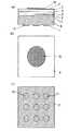
図1(a)は第1実施形態の半導体発光素子の側面図であり、図1(b)は上記半導体発光素子の上面図であり、図1(c)は上記半導体発光素子の底面図である。(1st Embodiment)
FIG. 1A is a side view of the semiconductor light emitting device of the first embodiment, FIG. 1B is a top view of the semiconductor light emitting device, and FIG. 1C is a bottom view of the semiconductor light emitting device. is there.
図1(a)に示すように、この半導体発光素子は、n型のGaP基板8の一方の面(図1における上面)の上に、下から順に、n型のGaPキャップ層(厚さ1μm)7、n型の(Al0.2Ga0.8)0.77In0.23P中間層(厚さ0.15μm)6、n型の(Al0.7Ga0.3)0.5In0.5Pクラッド層(厚さ1μm)5、発光層としてのp型の量子井戸活性層4、p型の(Al0.7Ga0.3)0.5In0.5Pクラッド層(厚さ1μm)3、酸化亜鉛からなる透光性電極層9を備えている。さらに、GaP基板8の他方の面(図1における底面)に第1の電極としてAuSiからなるn型電極11が設けられる一方、透光性電極層9の表面(図1における上面)に第2の電極としてAuからなるボンディングパッド10が設けられている。As shown in FIG. 1A, this semiconductor light emitting device has an n-type GaP cap layer (having a thickness of 1 μm) on one surface (upper surface in FIG. 1) of an n-
図1(c)に示すように、n型電極11は、それぞれ直径30μmの比較的小さい円形にパターン加工され、底面に行列状に複数(この例では3行3列の計9個)配置されている。一方、図1(b)に示すように、ボンディングパッド10は、直径120μmの比較的大きい円形にパターン加工され、上面の中央に1個配置されている。 As shown in FIG. 1C, the n-
量子井戸活性層4は、詳細には図示しないが、(Al0.5Ga0.5)0.5In0.5Pからなるバリア層と、GaInPからなる井戸層とを交互に複数積層して構成されている。発光層としての量子井戸活性層4が(AlyGa1-y)zIn1-zP(ただし、0≦y≦1、0≦z≦1である。)からなれば、550nmから670nmの発光波長が得られる。Although not shown in detail, the quantum well
この半導体発光素子は次のようにして作製される。 This semiconductor light emitting device is manufactured as follows.
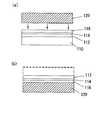
i) まず、図2に示すように、第1の半導体基板としてのn型GaAs基板1の一方の面(図2における上面)の上に、p型のGaAsバッファ層(厚さ1μm)2、p型の(Al0.7Ga0.3)0.5In0.5Pクラッド層(厚さ1μm)3、p型の量子井戸活性層4、n型の(Al0.7Ga0.3)0.5In0.5Pクラッド層(厚さ1μm)5、n型の(Al0.2Ga0.8)0.77In0.23P中間層(厚さ0.15μm)6、n型のGaPキャップ層(厚さ2μm)7を、MOCVD(有機金属気相成長)法により順次成長させて積層する。なお、成長方法としては、MOCVD法の他にMBE(分子線エピタキシ)法、MOMBE(有機金属分子線エピタキシ)法等の色々な方法が利用可能である。i) First, as shown in FIG. 2, on one surface (upper surface in FIG. 2) of an n-
上記p型の(Al0.7Ga0.3)0.5In0.5Pクラッド層3を成長させるとき、このクラッド層3のうちGaAsバッファ層2に接する厚さ0.1μm分のキャリア濃度は2×1018cm-3に設定し、量子井戸活性層4に接する厚さ0.9μm分のキャリア濃度は5×1017cm-3に設定する。When the p-type (Al0.7 Ga0.3 )0.5 In0.5 P clad
また、p型ドーパントにはZn、n型ドーパントにはSiを使用する。 Zn is used for the p-type dopant, and Si is used for the n-type dopant.
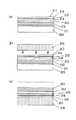
ii) 次に、この状態の基板(ウエハ)の表面をポリッシュにより鏡面加工した後、硫酸:過酸化水素系のエッチング液で少しエッチングする処理を行う。また、第2の半導体基板としての表面が鏡面であるn型のGaP基板8を用意し、このGaP基板8の表面を同じように硫酸:過酸化水素系のエッチング液で少しエッチングする処理を行う。そして、2枚の基板(ウエハ)を十分に純水洗浄、乾燥した後、図3に示すように、ウエハどうしを加圧状態で密着させ、800℃で1時間水素雰囲気中で熱処理する。こうすることにより、GaAs基板1上のn型GaPキャップ層7の表面(図3における上面)とn型GaP基板8の一方の面とが、つまりn型のGaPどうしが直接接合される。 ii) Next, after the surface of the substrate (wafer) in this state is mirror-finished by polishing, a process of slightly etching with a sulfuric acid: hydrogen peroxide based etchant is performed. Also, an n-
このような直接接合を行えば、n型GaP基板8の厚さを、機械的強度の観点から十分なレベルに容易に設定できる。 By performing such direct bonding, the thickness of the n-
iii) 次に、図4に示すように、アンモニア:過酸化水素系のエッチング液を用いて、n型のGaAs基板1及びp型のGaAsバッファ層2をエッチングして除去する。その後、n型GaP基板8の他方の面(図4における底面)を研磨して目標の厚さにする。 iii) Next, as shown in FIG. 4, the n-
iv) 次に、図1(a)に示すように、p型の(Al0.7Ga0.3)0.5In0.5Pクラッド層3の表面上に酸化亜鉛からなる透光性電極層9を形成し、更にその上にAuからなるボンディングパッド10を形成する。最後に、n型のGaP基板8の底面にAuSiからなる9個の円形状のn型電極11を形成する。iv) Next, as shown in FIG. 1A, a light-transmitting
このようにして作製された半導体発光素子について、ボンディングパッド10とn型電極11との間の通電電流が20mAという条件下で外部量子効率を評価したところ、外部量子効率が11%であった。これに対して、厚さ5μmのp型のAlGaAs電流拡散層を備えた従来構造の半導体発光素子では、同じ条件下で、外部量子効率が7.8%程度であった。この結果から、本実施形態の半導体発光素子では、外部量子効率が従来に比して約1.5倍に向上したことが分かる。 When the external quantum efficiency of the semiconductor light-emitting device manufactured in this manner was evaluated under the condition that the current flowing between the
このように素子特性が改善された理由は、n型のGaAs基板1およびn型のGaP基板8を使用して、p型の基板を使用しなかったこと、また、本実施形態の半導体発光素子はZnドープのp型のAlGaAs電流拡散層を備えていないことによる。つまり、高温となるエピタキシャル成長中、直接接合中に、p型ドーパントであるZnが発光層4へ拡散して内部量子効率を低下させるのを最小限に抑えたからである。また、透光性電極層9のお蔭で通電電流が拡散されて、発光層へ均一に電流が注入されるので、内部量子効率が高まる。 The reason why the device characteristics are improved is that the n-
さらに、本実施形態の半導体発光素子は、発光層4の上下に、それぞれこの発光層4の発光波長に対して透明な透光性電極層9、GaP基板8を備えているので、素子の上面および側面から外部へ光を取り出すことができ、発光波長に対して不透明な基板を用いた場合に比して光取り出し効率が高まる。また、GaPキャップ層7がGaP基板8に接しているので、GaP層/GaP基板の間でのヘテロ接合によるVF(順電圧)上昇が生じない。 Further, the semiconductor light emitting device of the present embodiment includes a
これらの結果、半導体発光素子の特性が向上して、高輝度が実現される。 As a result, the characteristics of the semiconductor light emitting element are improved, and high luminance is realized.
また、本実施形態の半導体発光素子では、通電電流20mAでの動作電圧は2.3Vであった。この動作電圧は、透光性電極層9とp型の(Al0.7Ga0.3)0.5In0.5Pクラッド層3との間に、キャリア濃度が5×1018cm-3で厚さ0.2μmのp型Al.0.5Ga0.5As層(p型コンタクト層)を設けることにより、半導体発光素子の輝度を維持したまま、2.1Vまで低減することができる。In the semiconductor light emitting device of the present embodiment, the operating voltage at a current of 20 mA was 2.3 V. This operating voltage is between the
この理由は、上記p型コンタクト層が1×1018cm-3以上のキャリア濃度を有すれば、素子の動作時に、上記透光性電極層と上記p型コンタクト層との界面での電圧降下を小さくすることができるからである。The reason is that if the p-type contact layer has a carrier concentration of 1 × 1018 cm−3 or more, the voltage drop at the interface between the translucent electrode layer and the p-type contact layer during the operation of the device. Can be reduced.
上記p型コンタクト層は、上記発光層の発光波長に対して透明なAlxGa1-xAs層(ただし、0.5≦x≦0.7である。)であるから、光取り出し効率を低下させることはない。Since the p-type contact layer is an Alx Ga1-x As layer (provided that 0.5 ≦ x ≦ 0.7) transparent to the emission wavelength of the light emitting layer, the light extraction efficiency is reduced. It does not lower.
また、上記p型コンタクト層のキャリア濃度を1×1019cm-3以下、より好ましくは5×1018cm-3以下に設定するとともに、このp型の半導体層の厚さを所定値以下に制限すれば、p型ドーパントの総量が制限されて、高温処理時のp型ドーパントの発光層への拡散が抑制される。したがって、内部量子効率の低下を抑制できる。これらの結果、半導体発光素子の外部量子効率(輝度)の低下を抑制できる。Further, the carrier concentration of the p-type contact layer is set to 1 × 1019 cm−3 or less, more preferably 5 × 1018 cm−3 or less, and the thickness of the p-type semiconductor layer is set to a predetermined value or less. If it is limited, the total amount of the p-type dopant is limited, and the diffusion of the p-type dopant into the light emitting layer during the high-temperature treatment is suppressed. Therefore, a decrease in internal quantum efficiency can be suppressed. As a result, a decrease in external quantum efficiency (luminance) of the semiconductor light emitting device can be suppressed.
具体的には、図5に示すように、上記p型コンタクト層の厚さを3μm以下に設定すれば、半導体発光素子の外部量子効率(輝度)の低下を10%以下に抑制できる。 Specifically, as shown in FIG. 5, when the thickness of the p-type contact layer is set to 3 μm or less, a decrease in external quantum efficiency (luminance) of the semiconductor light emitting device can be suppressed to 10% or less.
なお、上記p型コンタクト層を設けるには、最初のMOCVD法による成長の際にp型のGaAsバッファ層2とp型の(Al0.7Ga0.3)0.5In0.5Pクラッド層3との間に上記p型コンタクト層を形成しておけば良い。The p-type contact layer is provided between the p-type
本実施形態では、p型の電流拡散層を設けないので、p型の5μmのAlGaAs電流拡散層を備えた従来構造の半導体発光素子に比べ、エピタキシャル成長させる層厚を約1/2に低減できる。したがって、成長装置のメンテナンス頻度を1/2に少なくでき、生産性を高めるとともに安全性を向上させることができる。 In the present embodiment, since the p-type current diffusion layer is not provided, the thickness of the layer to be epitaxially grown can be reduced to about 比 べ as compared with a semiconductor light emitting device having a p-
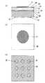
(第2実施形態)
図6(a)は第2実施形態の半導体発光素子の側面図であり、図6(b)は上記半導体発光素子の上面図であり、図6(c)は上記半導体発光素子の底面図である。(2nd Embodiment)
FIG. 6A is a side view of the semiconductor light emitting device of the second embodiment, FIG. 6B is a top view of the semiconductor light emitting device, and FIG. 6C is a bottom view of the semiconductor light emitting device. is there.
図6(a)に示すように、この半導体発光素子は、n型のGaP基板29の一方の面(図6における上面)の上に、下から順に、n型のGaPキャップ層(厚さ1μm)28、n型の(Al0.2Ga0.8)0.77In0.23P中間層(厚さ0.15μm)27、n型のAl0.5In0.5Pクラッド層(厚さ1μm)26、発光層としてのp型の量子井戸活性層25、p型のAl0.5In0.5Pクラッド層(厚さ1μm)24、p型の(Al0.5Ga0.5)0.5In0.5Pコンタクト層(厚さ0.2μm)23、酸化亜鉛からなる透光性電極層30を備えている。さらに、GaP基板29の他方の面(図6における底面)に第1の電極としてAuSiからなるn型電極32が設けられる一方、透光性電極層30の表面(図6における上面)に第2の電極としてAuからなるボンディングパッド31が設けられている。As shown in FIG. 6 (a), this semiconductor light emitting device has an n-type GaP cap layer (1 μm thick) on one surface (upper surface in FIG. 6) of an n-
図6(c)に示すように、n型電極32は、それぞれ直径30μmの比較的小さい円形にパターン加工され、底面に行列状に複数(この例では3行3列の計9個)配置されている。一方、図6(b)に示すように、ボンディングパッド31は、直径120μmの比較的大きい円形にパターン加工され、上面の中央に1個配置されている。 As shown in FIG. 6C, the n-
量子井戸活性層25は、詳細には図示しないが、(Al0.7Ga0.3)0.5In0.5Pからなるバリア層と、(Al0.3Ga0.7)0.5In0.5Pからなる井戸層とを交互に複数積層して構成されている。発光層としての量子井戸活性層25が(AlyGa1-y)zIn1-zP(ただし、0≦y≦1、0≦z≦1である。)からなれば、550nmから670nmの発光波長が得られる。Although not shown in detail, the quantum well
この半導体発光素子は次のようにして作製される。 This semiconductor light emitting device is manufactured as follows.
i) まず、図7に示すように、第1の半導体基板としてのn型GaAs基板21の一方の面(図7における上面)の上に、p型のGaAsバッファ層(厚さ1μm)22、p型の(Al0.5Ga0.5)0.5In0.5Pコンタクト層(厚さ0.2μm)23、p型のAl0.5In0.5Pクラッド層(厚さ1μm)24、p型の量子井戸活性層25、n型のAl0.5In0.5Pクラッド層(厚さ1μm)26、n型の(Al0.2Ga0.8)0.77In0.23P中間層(厚さ0.15μm)27、n型のGaPキャップ層(厚さ1μm)28を、MOCVD(有機金属気相成長)法により順次成長させて積層する。i) First, as shown in FIG. 7, a p-type GaAs buffer layer (1 μm in thickness) 22 is formed on one surface (upper surface in FIG. 7) of an n-
ii) 続いてその上に、図8に示すように、第2の半導体基板としてのn型のGaP層(これを「GaP基板」と呼ぶ。)29を、VPE法により、機械的強度の観点から十分なレベルの目標の厚さ、この例では約100μmの厚さまでエピタキシャル成長させる。 ii) Subsequently, as shown in FIG. 8, an n-type GaP layer 29 (referred to as a “GaP substrate”) as a second semiconductor substrate is formed thereon by a VPE method in terms of mechanical strength. To a sufficient level of target thickness, in this example about 100 μm.
iii) 次に、図9に示すように、アンモニア:過酸化水素系のエッチング液を用いて、n型のGaAs基板21及びp型のGaAsバッファ層22をエッチングして除去する。 iii) Next, as shown in FIG. 9, the n-
なお、n型GaP基板29をVPE法により目標の厚さに成長させているので、n型GaP基板29の厚さを調整するためにこの段階で研磨等を行う必要はない。したがって、直接接合によってGaP基板29を形成する場合に比して、製造工程を簡略化することができる。 Since the n-
iv) 次に、図6(a)に示すように、p型の(Al0.5Ga0.5)0.5In0.5Pコンタクト層23の表面上に酸化亜鉛からなる透光性電極層30を形成し、更にその上にAuからなるボンディングパッド31を形成する。最後に、n型のGaP基板29の底面にAuSiからなる9個の円形状のn型電極32を形成する。iv) Next, as shown in FIG. 6A, a
このようにして作製された半導体発光素子について、ボンディングパッド31とn型電極32との間の通電電流が20mAという条件下で外部量子効率を評価したところ、外部量子効率が4.2%であった。これに対して、厚さ5μmのp型のAlGaAs電流拡散層を備えた従来構造の半導体発光素子では、同じ条件下で、外部量子効率が3.0%程度であった。この結果から、本実施形態の半導体発光素子では、外部量子効率が従来に比して約1.4倍に向上したことが分かる。 When the external quantum efficiency of the semiconductor light emitting device thus manufactured was evaluated under the condition that the current flowing between the
本実施形態では、コンタクト層としてp型の(Al0.5Ga0.5)0.5In0.5P層を使用したが、発光波長に対して、十分吸収が小さければGa0.5In0.5PのようなさらにAl混晶比の小さな組成の層をコンタクト層として使用してもよい。Al混晶比が小さい方が、表面が酸化されにくくなり、更に高いドーピング濃度が可能になる。そのようにした場合、上記透光性電極層と上記p型の半導体層との界面での電圧降下を小さくすることができ、素子の歩留まりを高めることができる。また、第1実施形態と同様に、GaPキャップ層28がGaP基板29に接しているので、GaP層/GaP基板の間でのヘテロ接合によるVF(順電圧)上昇が生じない。In this embodiment, a p-type (Al0.5 Ga0.5 )0.5 In0.5 P layer is used as the contact layer. However, if the absorption is sufficiently small with respect to the emission wavelength, an Al mixed crystal such as Ga0.5 In0.5 P is further used. A layer having a low composition ratio may be used as the contact layer. The smaller the Al mixed crystal ratio, the harder the surface is oxidized, and a higher doping concentration becomes possible. In such a case, the voltage drop at the interface between the translucent electrode layer and the p-type semiconductor layer can be reduced, and the yield of the device can be increased. Further, similarly to the first embodiment, since the
上述の各実施形態では、第1の半導体基板として、Siドープのn型GaAs基板を使用したが、これに限られるものではない。ノンドープ型あるいは発光層への拡散が実質的に無視できるような弱いp型のGaAs基板であっても、同様の効果が得られる。熱履歴にも依存するが、発光層への拡散が実質的に無視できるような「弱いp型のGaAs基板」であるためには、GaAs基板中のp型キャリア濃度が例えば1×1018cm-3以下、好ましくは5×1017cm-3以下、より好ましくは1×1017cm-3以下であれば良い。上述の各実施形態で述べたような熱履歴の場合、GaAs基板中のp型キャリア濃度が5×1017cm-3程度以下であれば、発光層への拡散は十分に小さいと考えられる。第1の半導体基板がGaAs基板であれば、GaAs基板に格子整合する材料系の半導体層を備えた高輝度の半導体発光素子を作製することが可能になる。In each of the above embodiments, the n-type GaAs substrate doped with Si is used as the first semiconductor substrate, but the present invention is not limited to this. The same effect can be obtained even with a non-doped or weak p-type GaAs substrate in which diffusion into the light emitting layer is substantially negligible. Although it depends on the thermal history, in order to be a “weak p-type GaAs substrate” in which diffusion into the light emitting layer can be substantially ignored, the p-type carrier concentration in the GaAs substrate is, for example, 1 × 1018 cm.-3 or less, preferably 5 × 1017 cm-3 or less, more preferably 1 × 1017 cm-3 or less. In the case of the thermal history described in each of the above embodiments, if the p-type carrier concentration in the GaAs substrate is about 5 × 1017 cm−3 or less, diffusion into the light emitting layer is considered to be sufficiently small. When the first semiconductor substrate is a GaAs substrate, a high-luminance semiconductor light-emitting element including a material-based semiconductor layer lattice-matched to the GaAs substrate can be manufactured.
上記透光性電極層の材料は酸化亜鉛に限られず、酸化インジウム、酸化錫、酸化インジウム錫、または酸化マグネシウムからなっていても良い。透光性電極層が酸化インジウム、酸化錫、酸化インジウム錫、酸化亜鉛、または酸化マグネシウムの少なくとも1つからなれば、可視光に対して90%以上の透過率を得ることができる。したがって、さらに高輝度を実現できる。 The material of the translucent electrode layer is not limited to zinc oxide, and may be made of indium oxide, tin oxide, indium tin oxide, or magnesium oxide. When the translucent electrode layer is made of at least one of indium oxide, tin oxide, indium tin oxide, zinc oxide, and magnesium oxide, a transmittance of 90% or more to visible light can be obtained. Therefore, higher luminance can be realized.
1,21 n型GaAs基板
2,22 p型GaAsバッファ層
23 p型コンタクト層
3,24 クラッド層
4,25 量子井戸活性層
5,26 クラッド層
6,27 n型中間層
7,28 n型GaPキャップ層
8,29 n型GaP基板
9,30 透光性電極層
10,31 p型電極
11,32 n型電極1,21 n-
Claims (9)
Translated fromJapaneseその発光層上に単層または複数層からなるn型の半導体層を積層する工程と、
上記n型の半導体層の表面に上記発光層の発光波長に対して透明な第2の半導体基板を形成する工程と、
その後上記第1の半導体基板を除去する工程と、
上記第1の半導体基板の除去によって露出した面に上記発光層の発光波長に対して透明な透光性電極層を形成する工程を有することを特徴とする半導体発光素子の製造方法。Stacking a light-emitting layer made of a single layer or a plurality of semiconductors on a non-doped, weak p-type or n-type first semiconductor substrate;
Stacking an n-type semiconductor layer consisting of a single layer or a plurality of layers on the light emitting layer;
Forming a second semiconductor substrate transparent to the emission wavelength of the light emitting layer on the surface of the n-type semiconductor layer;
Then removing the first semiconductor substrate;
A method for manufacturing a semiconductor light emitting device, comprising a step of forming a transparent electrode layer transparent to an emission wavelength of the light emitting layer on a surface exposed by removing the first semiconductor substrate.
上記発光層を積層する工程の前に、上記第1の半導体基板上に、この第1の半導体基板上とは組成が異なる単層または複数層からなるp型の半導体層を形成する工程を有することを特徴とする半導体発光素子の製造方法。The method for manufacturing a semiconductor light emitting device according to claim 1,
Forming a p-type semiconductor layer having a single layer or a plurality of layers having a different composition from the first semiconductor substrate on the first semiconductor substrate before the step of laminating the light emitting layer; A method for manufacturing a semiconductor light emitting device, comprising:
上記第2の半導体基板を直接接合によって形成することを特徴とする半導体発光素子の製造方法。The method for manufacturing a semiconductor light emitting device according to claim 1,
A method for manufacturing a semiconductor light emitting device, wherein the second semiconductor substrate is formed by direct bonding.
上記第2の半導体基板をエピタキシャル成長によって形成することを特徴とする半導体発光素子の製造方法。The method for manufacturing a semiconductor light emitting device according to claim 1,
A method for manufacturing a semiconductor light emitting device, wherein the second semiconductor substrate is formed by epitaxial growth.
上記p型の半導体層は、1×1018cm-3以上1×1019cm-3以下のキャリア濃度を有し、上記発光層の発光波長に対して透明なAlxGa1-xAs層(ただし、0.5≦x≦0.7である。)を含むことを特徴とする半導体発光素子の製造方法。The method for manufacturing a semiconductor light emitting device according to claim 2,
The p-type semiconductor layer has a carrier concentration of 1 × 1018 cm−3 or more and 1 × 1019 cm−3 or less, and is an Alx Ga1 -x As layer transparent to the emission wavelength of the light emitting layer. (Provided that 0.5 ≦ x ≦ 0.7).
上記p型の半導体層は、1×1018cm-3以上1×1019cm-3以下のキャリア濃度を有し、上記発光層の発光波長に対して透明な(AlyGa1-y)zIn1-zP層(ただし、0≦y≦1、0≦z≦1である。)を含むことを特徴とする半導体発光素子の製造方法。The method for manufacturing a semiconductor light emitting device according to claim 2,
The p-type semiconductor layer of, 1 × 1018 cm-3 or more 1 × 1019 cm-3 has the following carrier concentration, transparent to the emission wavelength of the light emitting layer (Aly Ga1-y)z in1-z P layers (provided that 0 ≦ y ≦ 1,0 ≦ z ≦ 1.) the method of manufacturing a semiconductor light-emitting device, which comprises a.
上記p型の半導体層の厚さが3μm以下であることを特徴とする半導体発光素子の製造方法。The method for manufacturing a semiconductor light emitting device according to claim 2,
A method for manufacturing a semiconductor light emitting device, wherein the thickness of the p-type semiconductor layer is 3 μm or less.
上記単層または複数層からなる発光層は直接接合によりGaP基板上に形成され、
上記GaP基板の他方の面に第1の電極が設けられる一方、
上記透光性電極層と接続されるように第2の電極が設けられていることを特徴とする半導体発光素子。A light-emitting layer composed of a single layer or a plurality of layers and a light-transmitting electrode layer are laminated in this order on one surface of the GaP substrate, and the GaP substrate and the light-transmitting electrode layer are transparent to the light-emitting wavelength of the light-emitting layer. Has become
The single or multiple light emitting layer is formed on a GaP substrate by direct bonding,
While the first electrode is provided on the other surface of the GaP substrate,
A semiconductor light-emitting element, wherein a second electrode is provided so as to be connected to the light-transmitting electrode layer.
9. The semiconductor light emitting device according to claim 8, wherein a GaP layer is provided between the GaP substrate and a single layer or a plurality of light emitting layers, and the GaP layer is in contact with the GaP substrate.
Priority Applications (2)
| Application Number | Priority Date | Filing Date | Title |
|---|---|---|---|
| JP2003292127AJP2004153241A (en) | 2002-10-11 | 2003-08-12 | Semiconductor light emitting device and method of manufacturing the same |
| US10/684,127US20040126918A1 (en) | 2002-10-11 | 2003-10-14 | Semiconductor light emitting device and method for manufacturing same |
Applications Claiming Priority (2)
| Application Number | Priority Date | Filing Date | Title |
|---|---|---|---|
| JP2002299244 | 2002-10-11 | ||
| JP2003292127AJP2004153241A (en) | 2002-10-11 | 2003-08-12 | Semiconductor light emitting device and method of manufacturing the same |
Publications (1)
| Publication Number | Publication Date |
|---|---|
| JP2004153241Atrue JP2004153241A (en) | 2004-05-27 |
Family
ID=32473608
Family Applications (1)
| Application Number | Title | Priority Date | Filing Date |
|---|---|---|---|
| JP2003292127APendingJP2004153241A (en) | 2002-10-11 | 2003-08-12 | Semiconductor light emitting device and method of manufacturing the same |
Country Status (2)
| Country | Link |
|---|---|
| US (1) | US20040126918A1 (en) |
| JP (1) | JP2004153241A (en) |
Cited By (2)
| Publication number | Priority date | Publication date | Assignee | Title |
|---|---|---|---|---|
| JP2011198807A (en)* | 2010-03-17 | 2011-10-06 | Shin Etsu Handotai Co Ltd | Compound semiconductor substrate, light emitting element, method of manufacturing compound semiconductor substrate, and method of manufacturing light emitting element |
| WO2012120798A1 (en)* | 2011-03-09 | 2012-09-13 | 信越半導体株式会社 | Compound semiconductor substrate, method for producing compound semiconductor substrate, and light-emitting element |
Families Citing this family (25)
| Publication number | Priority date | Publication date | Assignee | Title |
|---|---|---|---|---|
| US7670872B2 (en)* | 2004-10-29 | 2010-03-02 | LED Engin, Inc. (Cayman) | Method of manufacturing ceramic LED packages |
| US8324641B2 (en)* | 2007-06-29 | 2012-12-04 | Ledengin, Inc. | Matrix material including an embedded dispersion of beads for a light-emitting device |
| US8134292B2 (en)* | 2004-10-29 | 2012-03-13 | Ledengin, Inc. | Light emitting device with a thermal insulating and refractive index matching material |
| US9929326B2 (en) | 2004-10-29 | 2018-03-27 | Ledengin, Inc. | LED package having mushroom-shaped lens with volume diffuser |
| US8816369B2 (en) | 2004-10-29 | 2014-08-26 | Led Engin, Inc. | LED packages with mushroom shaped lenses and methods of manufacturing LED light-emitting devices |
| US7772609B2 (en)* | 2004-10-29 | 2010-08-10 | Ledengin, Inc. (Cayman) | LED package with structure and materials for high heat dissipation |
| US8075165B2 (en)* | 2008-10-14 | 2011-12-13 | Ledengin, Inc. | Total internal reflection lens and mechanical retention and locating device |
| US20100117106A1 (en)* | 2008-11-07 | 2010-05-13 | Ledengin, Inc. | Led with light-conversion layer |
| US8507300B2 (en)* | 2008-12-24 | 2013-08-13 | Ledengin, Inc. | Light-emitting diode with light-conversion layer |
| US7985000B2 (en)* | 2009-04-08 | 2011-07-26 | Ledengin, Inc. | Lighting apparatus having multiple light-emitting diodes with individual light-conversion layers |
| CN101894901B (en) | 2009-04-08 | 2013-11-20 | 硅谷光擎 | Package for multiple light emitting diodes |
| US8598793B2 (en) | 2011-05-12 | 2013-12-03 | Ledengin, Inc. | Tuning of emitter with multiple LEDs to a single color bin |
| US8303141B2 (en)* | 2009-12-17 | 2012-11-06 | Ledengin, Inc. | Total internal reflection lens with integrated lamp cover |
| US9080729B2 (en) | 2010-04-08 | 2015-07-14 | Ledengin, Inc. | Multiple-LED emitter for A-19 lamps |
| US9345095B2 (en) | 2010-04-08 | 2016-05-17 | Ledengin, Inc. | Tunable multi-LED emitter module |
| US8858022B2 (en) | 2011-05-05 | 2014-10-14 | Ledengin, Inc. | Spot TIR lens system for small high-power emitter |
| US8513900B2 (en) | 2011-05-12 | 2013-08-20 | Ledengin, Inc. | Apparatus for tuning of emitter with multiple LEDs to a single color bin |
| US11032884B2 (en) | 2012-03-02 | 2021-06-08 | Ledengin, Inc. | Method for making tunable multi-led emitter module |
| US9897284B2 (en) | 2012-03-28 | 2018-02-20 | Ledengin, Inc. | LED-based MR16 replacement lamp |
| US9234801B2 (en) | 2013-03-15 | 2016-01-12 | Ledengin, Inc. | Manufacturing method for LED emitter with high color consistency |
| US9406654B2 (en) | 2014-01-27 | 2016-08-02 | Ledengin, Inc. | Package for high-power LED devices |
| CN107004677B (en) | 2014-11-26 | 2020-08-25 | 硅谷光擎 | Compact transmitter for warm dimming and color-tunable lamps |
| US9530943B2 (en) | 2015-02-27 | 2016-12-27 | Ledengin, Inc. | LED emitter packages with high CRI |
| US10219345B2 (en) | 2016-11-10 | 2019-02-26 | Ledengin, Inc. | Tunable LED emitter with continuous spectrum |
| US10575374B2 (en) | 2018-03-09 | 2020-02-25 | Ledengin, Inc. | Package for flip-chip LEDs with close spacing of LED chips |
Family Cites Families (5)
| Publication number | Priority date | Publication date | Assignee | Title |
|---|---|---|---|---|
| US5008718A (en)* | 1989-12-18 | 1991-04-16 | Fletcher Robert M | Light-emitting diode with an electrically conductive window |
| JP3324102B2 (en)* | 1993-11-22 | 2002-09-17 | 信越半導体株式会社 | Manufacturing method of epitaxial wafer |
| US5869849A (en)* | 1995-10-05 | 1999-02-09 | Industry Technology Research Institute | Light-emitting diodes with high illumination |
| JP3698402B2 (en)* | 1998-11-30 | 2005-09-21 | シャープ株式会社 | Light emitting diode |
| TW497277B (en)* | 2000-03-10 | 2002-08-01 | Toshiba Corp | Semiconductor light emitting device and method for manufacturing the same |
- 2003
- 2003-08-12JPJP2003292127Apatent/JP2004153241A/enactivePending
- 2003-10-14USUS10/684,127patent/US20040126918A1/ennot_activeAbandoned
Cited By (2)
| Publication number | Priority date | Publication date | Assignee | Title |
|---|---|---|---|---|
| JP2011198807A (en)* | 2010-03-17 | 2011-10-06 | Shin Etsu Handotai Co Ltd | Compound semiconductor substrate, light emitting element, method of manufacturing compound semiconductor substrate, and method of manufacturing light emitting element |
| WO2012120798A1 (en)* | 2011-03-09 | 2012-09-13 | 信越半導体株式会社 | Compound semiconductor substrate, method for producing compound semiconductor substrate, and light-emitting element |
Also Published As
| Publication number | Publication date |
|---|---|
| US20040126918A1 (en) | 2004-07-01 |
Similar Documents
| Publication | Publication Date | Title |
|---|---|---|
| JP2004153241A (en) | Semiconductor light emitting device and method of manufacturing the same | |
| JPH114020A (en) | Semiconductor light emitting element, method of manufacturing the same, and semiconductor light emitting device | |
| JP3207773B2 (en) | Compound semiconductor light emitting device and method of manufacturing the same | |
| US20020145147A1 (en) | Light emitting diode and manufacturing method thereof | |
| JP2008300719A (en) | Semiconductor light emitting device and manufacturing method thereof | |
| US7166865B2 (en) | Semiconductor light emitting device and method for manufacturing same | |
| US6552369B2 (en) | Light emitting diode and fabricating method thereof | |
| JP2006066518A (en) | Semiconductor light emitting device and method for manufacturing semiconductor light emitting device | |
| JP5229518B2 (en) | Manufacturing method of semiconductor light emitting diode | |
| TW202145551A (en) | Micro light emitting diode chip | |
| JP2007103613A (en) | Vertical cavity light emitting diode and method for manufacturing the same | |
| JP4121551B2 (en) | Light emitting device manufacturing method and light emitting device | |
| JP3239061B2 (en) | Light emitting diode and method of manufacturing the same | |
| KR100519753B1 (en) | Method for manufacturing light emitting device comprising compound semiconductor of GaN group | |
| JP4281569B2 (en) | Method for manufacturing epitaxial wafer for semiconductor light emitting device | |
| JP3507716B2 (en) | Method for manufacturing semiconductor light emitting device | |
| EP2101361B1 (en) | Semiconductor light emitting device and method for manufacturing same, and epitaxial wafer | |
| JP2005235798A (en) | Epitaxial wafer for light emitting diode and light emitting diode | |
| JP2007324579A (en) | Integrated semiconductor light emitting device and method of manufacturing the same | |
| JP3332785B2 (en) | Semiconductor light emitting device and method of manufacturing the same | |
| CN1319183C (en) | Semiconductor luminessent device and method for manufacturing semiconductor luminescent device | |
| JP4108439B2 (en) | Light emitting device manufacturing method and light emitting device | |
| JP2006032665A (en) | Light emitting diode | |
| JP2006135215A (en) | Manufacturing method of semiconductor light emitting device | |
| JP2007324577A (en) | Integrated semiconductor light emitting device and method of manufacturing the same |
Legal Events
| Date | Code | Title | Description |
|---|---|---|---|
| A621 | Written request for application examination | Free format text:JAPANESE INTERMEDIATE CODE: A621 Effective date:20050810 | |
| A977 | Report on retrieval | Free format text:JAPANESE INTERMEDIATE CODE: A971007 Effective date:20080616 | |
| A131 | Notification of reasons for refusal | Free format text:JAPANESE INTERMEDIATE CODE: A131 Effective date:20080624 | |
| A02 | Decision of refusal | Free format text:JAPANESE INTERMEDIATE CODE: A02 Effective date:20081021 |