JP2004138958A - Display device - Google Patents
Display deviceDownload PDFInfo
- Publication number
- JP2004138958A JP2004138958AJP2002305673AJP2002305673AJP2004138958AJP 2004138958 AJP2004138958 AJP 2004138958AJP 2002305673 AJP2002305673 AJP 2002305673AJP 2002305673 AJP2002305673 AJP 2002305673AJP 2004138958 AJP2004138958 AJP 2004138958A
- Authority
- JP
- Japan
- Prior art keywords
- display device
- switching regulator
- control circuit
- regulator control
- circuit
- Prior art date
- Legal status (The legal status is an assumption and is not a legal conclusion. Google has not performed a legal analysis and makes no representation as to the accuracy of the status listed.)
- Withdrawn
Links
Images


Classifications
- G—PHYSICS
- G09—EDUCATION; CRYPTOGRAPHY; DISPLAY; ADVERTISING; SEALS
- G09G—ARRANGEMENTS OR CIRCUITS FOR CONTROL OF INDICATING DEVICES USING STATIC MEANS TO PRESENT VARIABLE INFORMATION
- G09G3/00—Control arrangements or circuits, of interest only in connection with visual indicators other than cathode-ray tubes
- G09G3/20—Control arrangements or circuits, of interest only in connection with visual indicators other than cathode-ray tubes for presentation of an assembly of a number of characters, e.g. a page, by composing the assembly by combination of individual elements arranged in a matrix no fixed position being assigned to or needed to be assigned to the individual characters or partial characters
- G—PHYSICS
- G09—EDUCATION; CRYPTOGRAPHY; DISPLAY; ADVERTISING; SEALS
- G09G—ARRANGEMENTS OR CIRCUITS FOR CONTROL OF INDICATING DEVICES USING STATIC MEANS TO PRESENT VARIABLE INFORMATION
- G09G2300/00—Aspects of the constitution of display devices
- G09G2300/04—Structural and physical details of display devices
- G09G2300/0404—Matrix technologies
- G09G2300/0408—Integration of the drivers onto the display substrate
- G—PHYSICS
- G09—EDUCATION; CRYPTOGRAPHY; DISPLAY; ADVERTISING; SEALS
- G09G—ARRANGEMENTS OR CIRCUITS FOR CONTROL OF INDICATING DEVICES USING STATIC MEANS TO PRESENT VARIABLE INFORMATION
- G09G2330/00—Aspects of power supply; Aspects of display protection and defect management
- G09G2330/02—Details of power systems and of start or stop of display operation
Landscapes
- Engineering & Computer Science (AREA)
- Physics & Mathematics (AREA)
- Computer Hardware Design (AREA)
- General Physics & Mathematics (AREA)
- Theoretical Computer Science (AREA)
- Control Of Indicators Other Than Cathode Ray Tubes (AREA)
- Control Of El Displays (AREA)
- Liquid Crystal (AREA)
- Liquid Crystal Display Device Control (AREA)
- Devices For Indicating Variable Information By Combining Individual Elements (AREA)
- Dc-Dc Converters (AREA)
Abstract
Description
Translated fromJapanese【0001】
【発明の属する技術分野】
本発明は、電源回路を有する表示装置に関し、特にスイッチングレギュレータ制御回路を薄膜トランジスタで形成した表示装置に関する。
【0002】
【従来の技術】
近年、通信技術の進歩に伴って、携帯電話が普及している。今後は更に動画の伝送やより多くの情報伝達が予想される。一方、パーソナルコンピュータもその軽量化によって、モバイル対応の製品が生産されている。電子手帳に始まったPDAと呼ばれる情報端末も多数生産され普及しつつある。また、表示装置の発展により、それらの携帯情報機器のほとんどにはフラットパネルディスプレイが装備されている。
【0003】
また、アクティブマトリクス型の表示装置の中でも、近年、低温ポリシリコン薄膜トランジスタ(以下薄膜トランジスタをTFTと表記する)を用いた表示装置の製品化が進められている。低温ポリシリコンTFTでは画素だけでなく、画素部の周囲に信号線駆動回路を一体形成することが可能であるため、表示装置の小型化や、高精細化が可能であり、今後はさらに普及が見込まれる。
【0004】
ところが、従来の低温ポリシリコンTFTを用いた表示装置では、映像信号を画素に書き込む回路は内蔵していたが、電源回路などは内蔵されておらず、外付け部品として外部に装着されていた。
一般に携帯情報機器などの携帯用機器は、電源としてリチウムイオン電池を用いることが多い。リチウムイオン電池は通常3.6V程度の直流電圧を出力する電池で、寿命が長い、急速充電が可能、保持特性がよい、安全性が高いなどの理由によって広く使用されている。しかし、液晶や有機ELなどの表示装置に用いる材料を駆動するためには、3.6Vの電圧では不足であり、10V〜18V程度の電圧が必要となる。
そこで、従来では、図2に示すように、スイッチングレギュレータをプリント基板上に構成し、駆動に必要な電圧を供給していた。図2は従来のスイッチングレギュレータを備えた携帯情報機器の表示装置周辺の外形図である。基板213上に画素部204、ソース信号線駆動回路202、ゲート信号線駆動回路203を一体形成し、FPC205、対向基板212を装着し、プリント基板206上にスイッチングレギュレータ制御回路207、インダクタ208、スイッチング素子209、ダイオード210、平滑容量211を実装している。
【0005】
スイッチングレギュレータの詳細技術については非特許文献1参照。
【0006】
【非特許文献1】
佐藤守男著、「スイッチング電源設計入門」日刊工業新聞社刊、1998年11月25日
【0007】
【発明が解決しようとする課題】
前述したような従来の低温ポリシリコンTFTを用いた表示装置では、映像信号を画素部に書き込む機能としての回路を有してはいたが、電源回路は外付けになっており、外付け部品の増加や占有面積の増加によるセットサイズの増大を招いていた。
【0008】
【課題を解決するための手段】
以上のような問題を解決するため、本発明者らは、表示装置の基板上のポリシリコンTFTを用いてスイッチングレギュレータ制御回路を内蔵することを考えた。ポリシリコンTFTは、アモルファスTFTと異なり、高い駆動能力を有しているため、スイッチングレギュレータ制御回路も構成することが可能である。
【0009】
以下に本発明の構成を示す。
【0010】
本発明は、
基板上に薄膜トランジスタを有する表示装置において、
前記表示装置はスイッチングレギュレータ制御回路を有し、
前記スイッチングレギュレータ制御回路は前記薄膜トランジスタによって構成されることを特徴としている。
【0011】
本発明は、
基板上に薄膜トランジスタを有する表示装置において、
前記表示装置はスイッチングレギュレータ制御回路を有し、
前記スイッチングレギュレータ制御回路は前記薄膜トランジスタによって構成され、
前記スイッチングレギュレータ制御回路の出力信号によって、スイッチング素子を駆動し、昇圧もしくは降圧をおこなうことを特徴としている。
【0012】
本発明は、
基板上に薄膜トランジスタを有する表示装置において、
前記表示装置はスイッチングレギュレータ制御回路と、
スイッチング素子と、
インダクタと
ダイオードと
平滑容量とを有し
前記スイッチングレギュレータ制御回路は、前記平滑容量の電圧をフィードバックする電圧フィードバック回路と、前記スイッチング素子のスイッチングデューティを制御するデューティ制御回路を有することを特徴としている。
【0013】
本発明は、
上記表示装置において、
前記インダクタと、
前記ダイオードと、
前記平滑容量は、FPC上に実装されていることを特徴としている。
【0014】
上記表示装置において、
前記インダクタと、
前記ダイオードと、
前記平滑容量は、前記薄膜トランジスタが形成された基板上に実装されていることを特徴としている。
【0015】
本発明は、
上記表示装置において、
前記スイッチング素子は、薄膜トランジスタで構成されていることを特徴としている。
【0016】
本発明は、
基板上に薄膜トランジスタを形成した表示装置において、
前記表示装置はスイッチングレギュレータ制御回路を有し、
前記スイッチングレギュレータ制御回路は、
アナログ信号を用いたものであることを特徴とした表示装置。
【0017】
本発明は
上記表示装置において、
前記スイッチングレギュレータ制御回路は、
基準電圧源と、誤差増幅回路と、三角波発生回路と、PWMコンパレータを有することを特徴としている。
【0018】
本発明は
基板上に薄膜トランジスタを形成した表示装置において、
前記表示装置はスイッチングレギュレータ制御回路を有し、
前記スイッチングレギュレータ制御回路は、
デジタル信号を用いたものであることを特徴としている。
【0019】
本発明は
上記表示装置において、
前記スイッチングレギュレータ制御回路は、
AD変換回路と、不揮発性メモリと、CPUと、パルス発生回路を有することを特徴としている。
【0020】
本発明は、
上記表示装置において、
スイッチングレギュレータ制御回路は基板上に複数個構成されていることを特徴としている。
【0021】
本発明は
上記表示装置において、
前記表示装置は、液晶表示装置であることを特徴としている。
【0022】
本発明は、
上記表示装置において、
前記表示装置は、ELを用いた表示装置であることを特徴としている。
【0023】
本発明は、上記の表示装置を使用した電子機器である。
【0024】
以上によって、スイッチングレギュレータ制御回路の表示装置への内蔵化が達成でき、小型かつ軽量な電子機器を実現することができる。
【0025】
【発明の実施の形態】
以下、本発明の実施形態を、図面を用いて説明する。
【0026】
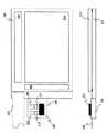
図1に本発明の表示装置の外形図を示す。本発明の表示装置101は、図1に示すように、基板112上に、画素部104、ソース信号線駆動回路102、ゲート信号線駆動回路103、スイッチングレギュレータ制御回路105をTFTで一体形成し、その上に、対向基板111を設置している。また、FPC106上には、インダクタ107、スイッチング素子108、ダイオード109、平滑コンデンサ110を有している。ここではこれらの素子をFPCに実装したが、FPC上には限定されず、基板112上、または基板111上、もしくは他の基板上であっても良い。また、スイッチング素子はその電流が少ない場合にはTFTで形成することも可能である。ここで、基板はガラス基板、プラスチック基板、ステンレス基板、シリコン基板などを使用することができる。
【0027】
このように、表示装置上に、スイッチングレギュレータ制御回路を一体形成することによって、従来の携帯情報装置において、課題であった携帯情報装置の小型軽量化という問題を解決することが可能になる。
【0028】
図3は本発明に用いるスイッチングレギュレータ制御回路のブロック図である。図3では基板300上に本発明のスイッチングレギュレータ制御回路301、ドライバ回路304が形成されている。図3には図示していないが、画素部や他の画像処理回路が同一基板上に形成されていてもかまわない。
【0029】
スイッチングレギュレータ制御回路301は電圧フィードバック回路302およびデューティ制御回路303の2つのブロックから構成されている。電圧フィードバック回路302はスイッチングレギュレータの出力電圧を入力し、その電圧に応じた信号をデューティ制御回路303に出力する。デューティ制御回路303は電圧フィードバック回路の信号に応じて、デューティを変化させたパルスを出力する。スイッチング素子306はデューティ制御回路303の出力パルスによってスイッチングをおこなう。スイッチング素子は図3ではNPNバイポーラトランジスタで表記しているが、MOSトランジスタの使用も可能であるし、極性を変えることも可能である。スイッチング素子がオンしている時間が長いほどインダクタ305に蓄積されるエネルギーが大きく、スイッチング素子306がオフしているときにダイオード307を介して平滑容量308への充電能力が大きくなる。
【0030】
スイッチングレギュレータの出力電圧(平滑容量308の電圧)が低下すると、電圧フィードバック回路302に入力される電圧が低下する。電圧フィードバック回路302はそのときに、デューティ制御回路303がデューティをあげるような信号を出力する。デューティ制御回路303はそれを受けて、スイッチング素子306を高いデューティで駆動する。それによって、インダクタ305にはエネルギーがより高く蓄積され、平滑容量の電圧を上げるように動作する。
【0031】
一方、スイッチングレギュレータの出力電圧(平滑容量308の電圧)が上昇すると、電圧フィードバック回路302に入力される電圧が上昇する。電圧フィードバック回路302はそのときに、デューティ制御回路303がデューティを下げるような信号を出力する。デューティ制御回路303はそれを受けて、スイッチング素子306を低いデューティで駆動する。それによって、インダクタ305にはエネルギーがより低く蓄積され、平滑容量の電圧を下げるように動作する。
【0032】
このようにして、スイッチングレギュレータの出力電圧は一定の電圧を保つことができる。たとえば3.6Vのリチウムイオン電池で構成された外部電源電圧を本発明によって16Vに昇圧し、ドライバ回路304の電源電圧として使用することが可能である。
また、以下に説明するが電圧フィードバック回路およびデューティ制御回路はアナログ、デジタルいずれの方式でも実現が可能である。以下の実施例において、それらを説明する。
【0033】
【実施例】
(実施例1)
図4にアナログ方式のスイッチングレギュレータ制御回路のブロック図を示す。図4に示したスイッチングレギュレータ制御回路は電圧フィードバック回路403がアッテネータ404と誤差増幅回路405から構成され、デューティ制御回路402が三角波発生回路407とPWMコンパレータ406から構成される。スイッチングレギュレータ出力電圧はアッテネータ404によって分圧される。アッテネータ404はなくとも良い。アッテネータ404で分圧された電圧は片側の入力を基準電圧に接続した誤差増幅回路のもう片側の入力に入る。ここで基準電圧と比較され差分が増幅される。PWMコンパレータ406は誤差増幅回路405の出力と三角波の比較を行い、誤差増幅回路405の出力が大きい場合はデューティが大きいパルスを出力する。これによって、前述したようにインダクタのエネルギー蓄積量が増加し、スイッチングレギュレータの出力電圧は上昇する。したがって、アッテネータ404の出力電圧も上昇し、基準電圧の値に近づく。誤差増幅回路の出力が小さい場合には以上と逆の動作がおこり、やはり、アッテネータ404の出力は基準電圧に近づく。
アッテネータ404のアッテネ−ト比が4:1であれば、スイッチングレギュレータの出力電圧は基準電圧の4倍となる。この値は任意に設定できる。
以上のようにして、本発明のアナログ方式のスイッチングレギュレータ制御回路は動作する。
【0034】
(実施例2)
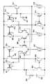
上述したような、アナログ方式のスイッチングレギュレータ制御回路においては、誤差増幅回路、PWMコンパレータをオペアンプ回路で構成することが多い。図5はTFTを用いて、オペアンプ回路を作成した場合の等価回路図である。このオペアンプは、TFT501、502で構成される差動回路、TFT503、TFT504で構成されるカレントミラー回路、TFT505、TFT509で構成される定電流源、TFT506で構成されるソース接地回路、TFT507、TFT508で構成されるアイドリング回路、TFT510、TFT511で構成されるソースフォロワ回路、位相補償コンデンサ512より成り立っている。
【0035】
以下に、図5のオペアンプ回路の動作を説明する。非反転端子に+信号が入力されると、差動回路を構成するTFTのソースにはTFT505で構成される定電流源が接続されているため、TFT501のドレイン電流がTFT502のドレイン電流より大きくなり、TFT503のドレイン電流は、TFT504とTFT503がカレントミラー回路を構成するため、TFT502のドレイン電流と同じになり、TFT503のドレイン電流とTFT501のドレイン電流の差電流によって、TFT506のゲート電位は低下する方向に変化する。TFT506はP型TFTであるので、TFT506のゲート電位が下がると、TFT506はよりオンする方向に動作し、ドレイン電流が増加する。よって、TFT510のゲート電位は上昇し、それに伴い、TFT510のソース電位すなわち、出力端子も上昇する。
【0036】
また、非反転入力端子に−信号が入力されると、TFT501のドレイン電流がTFT502のドレイン電流より小さくなり、TFT503のドレイン電流は、TFT502のドレイン電流と同じであるため、TFT503のドレイ電流とTFT501の差電流によって、TFT506のゲート電位は上昇する方向に変化する。TFT506はP型TFTであるので、TFT506のゲート電位が上がると、TFT506はオフする方向に動作し、ドレイン電流が減少する。よって、TFT510のゲート電位は低下し、それに伴い、TFT510のソース電位すなわち、出力端子も低下する。このように非反転入力端子の信号と同相の信号が、出力端子より出力される。
【0037】
反転入力端子に+信号が入力されると、TFT501のドレイン電流がTFT502のドレイン電流より小さくなり、TFT503のドレイン電流は、TFT502のドレイン電流と同じであるため、TFT503のドレイン電流とTFT501の差電流によって、TFT506のゲート電位は上昇する方向に変化する。TFT506はP型TFTであるので、TFT506のゲート電位が上がると、TFT506はオフする方向に動作し、ドレイン電流が減少する。よって、TFT510のゲート電位は低下し、それに伴い、TFT510のソース電位すなわち、出力端子も低下する。
【0038】
また、反転入力端子に−信号が入力されると、TFT501のドレイン電流がTFT502のドレイン電流より大きくなり、TFT503のドレイン電流は、TFT502のドレイン電流と同じであるため、TFT503のドレイン電流とTFT501のドレイン電流の差電流によって、TFT506のゲート電位は低下する方向に変化する。TFT506はP型TFTであるので、TFT506のゲート電位が下がると、TFT506はよりオンする方向に動作し、ドレイン電流が増加する。よって、TFT510のゲート電位は上昇し、それに伴い、TFT510のソース電位すなわち、出力端子も上昇する。このようにして、反転入力端子の信号と逆相の信号が出力端子より出力される。
【0039】
この例では、差動回路をNchTFT、カレントミラー回路をPchTFTで作成しているが、本発明では、それには限定されず逆であっても良い。また、回路形式もこのような回路接続には限定されることはなく、オペアンプ回路としての機能を満たすものであれば使用可能である。
また、本実施例は前述した実施例1と組み合わせて使用することが可能である。
【0040】
(実施例3)
図6はTFTで三角波発生回路を実現した例である。以下にその動作を説明する。まず、TFT607、608で構成される差動回路において、どちらか一方のTFTに電流が流れているとする。最初にTFT607のゲート電位がTFT608のゲート電位より高いとする。定電流620で決まる電流はTFT607、602に流れる。TFT601とTFT602はカレントミラー回路を構成しているため、TFT601にも同じ電流が流れる。TFT608はオフしているため、TFT604、603で構成されるカレントミラー回路、TFT606、605で構成されるカレントミラー回路もオフしている。よって、抵抗622にはTFT601から流れ込んだ電流によって、TFT607のゲート電位は基準電源623の電圧に、IR(電流源620の電流をI、抵抗622の抵抗値をRとする)を加えた電圧となる。
【0041】
一方、TFT615、616で構成される差動回路はそれぞれのゲートがTFT608、607のゲートに接続されているので、TFT616がオン、TFT615がオフとなる。したがって、電流源619の電流はTFT611、TFT616を介して流れることになる。TFT615がオフであるので、TFT609、610で構成されるカレントミラー回路、TFT613、614で構成されるカレントミラー回路もオフとなる。TFT612には電流源619と同じだけの電流が流れ、容量621を充電していく。容量にはTFT617によって構成されるソースフォロワが接続され、その出力がTFT608,615のゲートに接続される。容量621の電位が低い場合には、差動回路の状態は変化しないが、容量への充電が進み、電位が上昇し、TFT607、616のゲート電位をTFT608、615のゲート電位が超えると、オンオフが入れ替わる。
【0042】
TFT607のゲート電位がTFT608のゲート電位より低くなったとする。定電流620で決まる電流はTFT608、604に流れる。TFT603とTFT604はカレントミラー回路を構成しているため、TFT603にも同じ電流が流れる。同様にTFT605、606はカレントミラー回路であるため定電流620と等しい電流がTFT605に流れる。TFT607はオフしているため、TFT602、601で構成されるカレントミラー回路もオフしている。よって、抵抗622にはTFT605に引き込まれる電流によって、TFT607のゲート電位は基準電源623の電圧に、IR(電流源620の電流をI、抵抗622の抵抗値をRとする)を引いた電位となる。
【0043】
一方、TFT615、616で構成される差動回路はそれぞれのゲートがTFT608、607のゲートに接続されているので、TFT616がオフ、TFT615がオンとなる。したがって、電流源619の電流はTFT609、TFT615を介して流れることになる。TFT616がオフであるので、TFT611、612で構成されるカレントミラー回路もオフとなる。TFT610には電流源619と同じだけの電流が流れ、TFT613、614で構成されるカレントミラー回路を介して容量621を放電していく。容量にはTFT617によって構成されるソースフォロワが接続され、その出力がTFT608,615のゲートに接続される。容量621の電位が高い場合には、差動回路の状態は変化しないが、容量への放電が進み、電位が降下し、TFT607、616のゲート電位をTFT608、615のゲート電位が下回ると、オンオフが入れ替わる。その後これを繰り返す。
【0044】
このようにして、この回路は振幅が2IRの電圧で発振することとなる。容量621およびソースフォロワの出力電圧は、容量の電荷を定電流で充放電するので、電位が時間に対して直線的に変化し、三角波を得ることができる。本実施例は実施例1および2と組み合わせて使用することができる。
【0045】
(実施例4)
図7はデジタル方式のスイッチングレギュレータ制御回路701を示したものである。電圧フィードバック回路703はAD変換回路706、CPU705、不揮発性メモリ704によって構成されている。不揮発性メモリ704には必要なスイッチングレギュレータ電圧値に対応するデータが記憶されている。
スイッチングレギュレータ出力電圧はまずAD変換回路706で、アナログからデジタルに変換される。CPU705は不揮発性メモリ704から、求める電圧に相当するデータを呼び出し、そのデータとAD変換回路のデータを比較し、AD変換回路706の出力電圧が低ければ、デューティをあげるような指令をパルス発生回路707に出し、AD変換回路の出力電圧が高ければ、デューティを下げるような指令をパルス発生回路707に出す。
【0046】
図8はパルス発生回路707の内部構成を示したものである。図8においては、カウンタ回路801、ラッチ回路802、EXOR回路803〜806、AND回路807、NAND808、809で構成されるラッチ回路によって構成されている。まずCPUから、ある特定のデューティをあらわすデータが送られ、ラッチ回路802にラッチされる。ここでは4ビットを例にとり説明するが4ビットに限定するものではない。一方でクロックはカウンタ回路801に入力され、カウントがされていく。ここでカウンタ回路、ラッチ回路は公知の回路を使用可能であり、特に限定されない。
【0047】
図11にカウンタ出力とクロックの関連を示す。カウントが進んでいき、ラッチ回路にラッチされているデータとすべてのビットにおいて一致すると、EXORの出力はすべてハイになりANDの出力がハイになる。するとNAND808、809で構成されるラッチ回路のパルス回路出力はハイからロウに変わる。(カウンタが一周回ったときにリセットをかけ再度ハイにする。)図11ではラッチ回路の出力が1001の時に変化が起こる。ここでCPUから出力されるデータを0001とすればパルス回路出力がハイとなるのは最初のみとなり、デューティは1/16となる。またCPUから出力されるデータが1110となればデューティは14/16となる。
【0048】
このようにして、CPUから送られるデータを変えることにより、デューティを変化させることが可能になる。すなわち、スイッチングレギュレータ出力電圧が期待する値より小さい場合、CPUはパルス発生回路に送るデータをカウントアップして、デューティを上げ、電圧を上げることができる。また、スイッチングレギュレータ出力電圧が期待値より大きい場合は、CPUはパルス発生回路に送るデータをカウントダウンして、デューティを下げ、電圧を下げることができる。
図7、図8に示したように、デジタル方式スイッチングレギュレータ制御回路は動作することができる。ここでは上記の回路で説明を行ったが、回路構成は上記に限定されない。
【0049】
(実施例5)
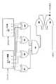
本発明のスイッチングレギュレータ制御回路はひとつの表示装置中に複数用いることが可能である。図9は本発明を3回路採用した例である。スイッチングレギュレータの電圧は内部の回路定数を帰ることによって、それぞれ異なるようにすることが可能である。EL表示装置などでは、RGBそれぞれのEL素子によって、必要な駆動電圧が異なるため、それぞれ個別な電源が必要である。
図9では基板922上に、画素部904、ソース信号線駆動回路902、ゲート信号線駆動回路903、スイッチングレギュレータ制御回路905、906、907を一体形成し、FPC908上にインダクタ909、913、917、スイッチング素子910、914、918、ダイオード911、915、919、平滑容量912、916、920を配置している。インダクタ、スイッチング素子、ダイオード、平滑容量はFPC上でなく基板上に設置してもよい。また、スイッチング素子はTFTで構成しても良い。
【0050】
また、複数の信号線駆動回路やその他の回路を有し、それぞれの回路に複数のスイッチングレギュレータより異なる電圧を供給しても良い。
【0051】
(実施例6)
図10は本発明のスイッチングレギュレータ制御回路を表示部とは異なる基板上に形成し、表示基板に貼り付けたものである。ここでスイッチングレギュレータ制御回路を形成した基板と表示基板は同じ材質によってできているものとする。このような構成をすることによって、以下の2つの利点が得られる。
基板の種類が同じなので、熱膨張係数の違いなどによって、クラックが発生するなどの信頼性悪化を防止できる。また、表示基板とスイッチングレギュレータ制御回路基板を別に製造できるため、表示基板はデザインルールのゆるい露光装置で、スイッチングレギュレータ制御回路基板はデザインルールの厳しい露光装置で製造が可能であり、スイッチングレギュレータ制御回路基板の面積縮小を行うことができる。
【0052】
図10では基板1012上に、画素部1004、ソース信号線駆動回路1002、ゲート信号線駆動回路1003を一体形成し、スイッチングレギュレータ制御回路1005を基板1012と同一材質の基板で形成し、装着する。FPC1006上にインダクタ1007、スイッチング素子1008、ダイオード1009、平滑容量1010を配置している。インダクタ、スイッチング素子、ダイオード、平滑容量はFPC上でなく基板上に設置してもよい。また、スイッチング素子はTFTで構成しても良い。
【0053】
また、本実施例は前述した実施例と組み合わせて使用することが可能である。
【0054】
(実施例7)
以上のようにして作製される表示装置は各種電子機器の表示部として用いることができる。以下に、本発明を用いて形成された表示装置を表示媒体として組み込んだ電子機器について説明する。
【0055】
その様な電子機器としては、ビデオカメラ、デジタルカメラ、ヘッドマウントディスプレイ(ゴーグル型ディスプレイ)、ゲーム機、カーナビゲーション、パーソナルコンピュータ、携帯情報端末(モバイルコンピュータ、携帯電話または電子書籍等)などが挙げられる。それらの一例を図12に示す。
【0056】
図12(A)はデジタルカメラであり、本体3101、表示部3102、受像部3103、操作キー3104、外部接続ポート3105、シャッター3106等を含む。本発明の表示装置はカメラの表示部3102に用いることができる。
【0057】
図12(B)はノートパソコンであり、本体3201、筐体3202、表示部3203、キーボード3204、外部接続ポート3205、ポインティングマウス3206等を含む。本発明の表示装置は表示部3203に使用することができる。
【0058】
図12(C)は携帯情報端末であり、本体3301、表示部3302、スイッチ3303、操作キー3304、赤外線ポート3305等を含む。本発明の表示装置は表示部3302に使用することができる。
【0059】
図12(D)は記録媒体を備えた画像再生装置(具体的にはDVD再生装置)であり、本体3401、筐体3402、記録媒体(CD、LDまたはDVD等)読込部3405、操作スイッチ3406、表示部(a)3403、表示部(b)3404等を含む。表示部Aは主として画像情報を表示し、表示部Bは主として文字情報を表示するが、本発明の表示装置は記録媒体を備えた画像再生装置の表示部(a)、(b)に用いることができる。なお、記録媒体を備えた画像再生装置としては、CD再生装置、ゲーム機器などに本発明を用いることができる。
【0060】
図12(E)は折りたたみ式携帯表示装置であり、本体3501に本発明を用いた表示部3502を装着することができる。
【0061】
図12(F)はビデオカメラであり、本体3601は、表示部3602、筐体3603、外部接続ポート3604、リモコン受信部3605、受像部3606、バッテリー3607、音声入力部3608、接眼部3609、操作キー3610などを含む。本発明の表示装置は表示部3602に用いることができる。
【0062】
図12(G)は携帯電話であり、本体3701は、筐体3702、表示部3703、音声入力部3704、アンテナ3705、操作キー3706、外部接続ポート3707などを含む。本発明の表示装置を表示部3703に用いることができる。
【0063】
以上の様に、本発明の適用範囲は極めて広く、あらゆる分野の電子機器に適用することが可能である。また、本実施例の電子機器は実施例1〜6のどのような組み合わせからなる構成を用いても実現することができる。
【0064】
【発明の効果】
従来の携帯情報機器では、スイッチングレギュレータ制御回路の縮小が困難であり、携帯情報機器の大きさを小さくすることができていなかった。
【0065】
本発明は、スイッチングレギュレータ制御回路をTFT基板上に、TFTを用いて一体形成することによって、体積の小さな表示装置を実現した。本発明によって、携帯情報機器の小型軽量化が可能となった。
【図面の簡単な説明】
【図1】本発明の表示装置の外形図。
【図2】従来の表示装置の外形図。
【図3】本発明のスイッチングレギュレータ制御回路のブロック図。
【図4】本発明のアナログスイッチングレギュレータ制御回路の図。
【図5】本発明のオペアンプ回路の等価回路図。
【図6】本発明の三角波発生回路の等価回路図
【図7】本発明のデジタルスイッチングレギュレータ制御回路の図。
【図8】本発明のパルス発生回路の図。
【図9】本発明のEL表示装置に本発明を応用した図。
【図10】本発明の表示装置の外形図。
【図11】本発明のパルス発生回路のタイミングチャート図。
【図12】本発明の表示装置を用いた電子機器の図。[0001]
TECHNICAL FIELD OF THE INVENTION
The present invention relates to a display device having a power supply circuit, and more particularly to a display device in which a switching regulator control circuit is formed using thin film transistors.
[0002]
[Prior art]
2. Description of the Related Art In recent years, with the progress of communication technology, mobile phones have become widespread. In the future, transmission of moving images and more information transmission are expected. On the other hand, as for personal computers, mobile-friendly products have been produced due to their light weight. A large number of information terminals called PDA, which began with electronic notebooks, are also being produced and are becoming popular. Also, due to the development of display devices, most of these portable information devices are equipped with flat panel displays.
[0003]
Further, among active matrix display devices, in recent years, a display device using a low-temperature polysilicon thin film transistor (hereinafter, a thin film transistor is referred to as a TFT) has been commercialized. In a low-temperature polysilicon TFT, not only pixels but also a signal line driving circuit can be integrally formed around a pixel portion, so that a display device can be miniaturized and a high definition can be achieved. Expected.
[0004]
However, in a conventional display device using a low-temperature polysilicon TFT, a circuit for writing a video signal to a pixel is built in, but a power supply circuit and the like are not built in, and the device is externally mounted as an external component.
Generally, portable devices such as portable information devices often use a lithium ion battery as a power source. Lithium-ion batteries are typically batteries that output a DC voltage of about 3.6 V, and are widely used because of their long life, quick charging, good retention characteristics, and high safety. However, a voltage of 3.6 V is insufficient for driving a material used for a display device such as a liquid crystal or an organic EL, and a voltage of about 10 V to 18 V is required.
Therefore, conventionally, as shown in FIG. 2, a switching regulator is configured on a printed circuit board to supply a voltage required for driving. FIG. 2 is an external view around a display device of a portable information device provided with a conventional switching regulator. A
[0005]
See
[0006]
[Non-patent document 1]
Morio Sato, "Introduction to Switching Power Supply Design", published by Nikkan Kogyo Shimbun, November 25, 1998
[0007]
[Problems to be solved by the invention]
A display device using a conventional low-temperature polysilicon TFT as described above has a circuit as a function of writing a video signal to a pixel portion, but a power supply circuit is externally provided, and external components are not provided. The increase in the set size due to the increase and the occupation area has been caused.
[0008]
[Means for Solving the Problems]
In order to solve the above problems, the present inventors have considered incorporating a switching regulator control circuit using a polysilicon TFT on a substrate of a display device. Since a polysilicon TFT has a high driving capability, unlike an amorphous TFT, a switching regulator control circuit can also be configured.
[0009]
Hereinafter, the configuration of the present invention will be described.
[0010]
The present invention
In a display device having a thin film transistor on a substrate,
The display device has a switching regulator control circuit,
The switching regulator control circuit is configured by the thin film transistor.
[0011]
The present invention
In a display device having a thin film transistor on a substrate,
The display device has a switching regulator control circuit,
The switching regulator control circuit is configured by the thin film transistor,
A switching element is driven by an output signal of the switching regulator control circuit to perform step-up or step-down.
[0012]
The present invention
In a display device having a thin film transistor on a substrate,
The display device is a switching regulator control circuit,
A switching element;
Inductor and
With diode
With smoothing capacity
The switching regulator control circuit includes a voltage feedback circuit that feeds back the voltage of the smoothing capacitor, and a duty control circuit that controls a switching duty of the switching element.
[0013]
The present invention
In the above display device,
Said inductor;
Said diode;
The smoothing capacitor is mounted on an FPC.
[0014]
In the above display device,
Said inductor;
Said diode;
The smoothing capacitor is mounted on a substrate on which the thin film transistor is formed.
[0015]
The present invention
In the above display device,
The switching element is characterized by being constituted by a thin film transistor.
[0016]
The present invention
In a display device in which a thin film transistor is formed on a substrate,
The display device has a switching regulator control circuit,
The switching regulator control circuit,
A display device using an analog signal.
[0017]
The present invention
In the above display device,
The switching regulator control circuit,
It is characterized by including a reference voltage source, an error amplification circuit, a triangular wave generation circuit, and a PWM comparator.
[0018]
The present invention
In a display device in which a thin film transistor is formed on a substrate,
The display device has a switching regulator control circuit,
The switching regulator control circuit,
It is characterized by using digital signals.
[0019]
The present invention
In the above display device,
The switching regulator control circuit,
It is characterized by including an AD conversion circuit, a nonvolatile memory, a CPU, and a pulse generation circuit.
[0020]
The present invention
In the above display device,
A plurality of switching regulator control circuits are provided on a substrate.
[0021]
The present invention
In the above display device,
The display device is a liquid crystal display device.
[0022]
The present invention
In the above display device,
The display device is a display device using EL.
[0023]
The present invention is an electronic device using the above display device.
[0024]
As described above, the switching regulator control circuit can be incorporated in the display device, and a small and lightweight electronic device can be realized.
[0025]
BEST MODE FOR CARRYING OUT THE INVENTION
Hereinafter, embodiments of the present invention will be described with reference to the drawings.
[0026]
FIG. 1 shows an external view of the display device of the present invention. In the
[0027]
As described above, by integrally forming the switching regulator control circuit on the display device, it is possible to solve the problem of reducing the size and weight of the portable information device, which has been a problem in the conventional portable information device.
[0028]
FIG. 3 is a block diagram of a switching regulator control circuit used in the present invention. In FIG. 3, a switching regulator control circuit 301 and a driver circuit 304 of the present invention are formed on a substrate 300. Although not shown in FIG. 3, the pixel portion and other image processing circuits may be formed on the same substrate.
[0029]
The switching regulator control circuit 301 includes two blocks of a voltage feedback circuit 302 and a duty control circuit 303. The voltage feedback circuit 302 receives the output voltage of the switching regulator and outputs a signal corresponding to the voltage to the duty control circuit 303. The duty control circuit 303 outputs a pulse whose duty has been changed according to the signal of the voltage feedback circuit. The switching
[0030]
When the output voltage of the switching regulator (the voltage of the smoothing capacitor 308) decreases, the voltage input to the voltage feedback circuit 302 decreases. At that time, the voltage feedback circuit 302 outputs a signal such that the duty control circuit 303 increases the duty. In response to this, the duty control circuit 303 drives the switching
[0031]
On the other hand, when the output voltage of the switching regulator (the voltage of the smoothing capacitor 308) increases, the voltage input to the voltage feedback circuit 302 increases. At that time, the voltage feedback circuit 302 outputs a signal such that the duty control circuit 303 reduces the duty. In response to this, the duty control circuit 303 drives the switching
[0032]
Thus, the output voltage of the switching regulator can be maintained at a constant voltage. For example, an external power supply voltage constituted by a 3.6 V lithium ion battery can be boosted to 16 V by the present invention and used as the power supply voltage of the driver circuit 304.
As will be described below, the voltage feedback circuit and the duty control circuit can be realized by any of analog and digital methods. These will be described in the following examples.
[0033]
【Example】
(Example 1)
FIG. 4 shows a block diagram of an analog switching regulator control circuit. In the switching regulator control circuit shown in FIG. 4, the voltage feedback circuit 403 includes an
If the attenuator ratio of the
As described above, the analog switching regulator control circuit of the present invention operates.
[0034]
(Example 2)
In an analog switching regulator control circuit as described above, an error amplifier circuit and a PWM comparator are often configured by an operational amplifier circuit. FIG. 5 is an equivalent circuit diagram when an operational amplifier circuit is formed using TFTs. This operational amplifier includes a differential circuit composed of
[0035]
Hereinafter, the operation of the operational amplifier circuit of FIG. 5 will be described. When a + signal is input to the non-inverting terminal, the drain current of the
[0036]
When a negative signal is input to the non-inverting input terminal, the drain current of the
[0037]
When the + signal is input to the inverting input terminal, the drain current of the
[0038]
When a negative signal is input to the inverting input terminal, the drain current of the
[0039]
In this example, the differential circuit is made of an NchTFT and the current mirror circuit is made of a PchTFT. However, the present invention is not limited to this, and may be reversed. Further, the circuit type is not limited to such a circuit connection, and any circuit that satisfies the function as an operational amplifier circuit can be used.
This embodiment can be used in combination with the first embodiment.
[0040]
(Example 3)
FIG. 6 shows an example in which a triangular wave generation circuit is realized by TFTs. The operation will be described below. First, in a differential circuit including the
[0041]
On the other hand, in the differential circuit composed of the
[0042]
It is assumed that the gate potential of the
[0043]
On the other hand, in the differential circuit composed of the
[0044]
In this way, the circuit oscillates at a voltage having an amplitude of 2IR. Since the output voltage of the
[0045]
(Example 4)
FIG. 7 shows a digital switching regulator control circuit 701. The voltage feedback circuit 703 includes an AD conversion circuit 706, a
The output voltage of the switching regulator is first converted by an AD conversion circuit 706 from analog to digital. The
[0046]
FIG. 8 shows the internal configuration of the pulse generation circuit 707. In FIG. 8, the latch circuit includes a
[0047]
FIG. 11 shows the relationship between the counter output and the clock. The count advances, and when all bits match the data latched in the latch circuit, the outputs of EXOR all go high and the outputs of AND go high. Then, the pulse circuit output of the latch circuit composed of the
[0048]
Thus, the duty can be changed by changing the data sent from the CPU. That is, when the output voltage of the switching regulator is smaller than the expected value, the CPU can count up data to be sent to the pulse generation circuit, increase the duty, and increase the voltage. When the switching regulator output voltage is higher than the expected value, the CPU can count down data to be sent to the pulse generation circuit, reduce the duty, and reduce the voltage.
As shown in FIGS. 7 and 8, the digital switching regulator control circuit can operate. Here, the description has been made using the above circuit, but the circuit configuration is not limited to the above.
[0049]
(Example 5)
A plurality of switching regulator control circuits of the present invention can be used in one display device. FIG. 9 shows an example in which the present invention employs three circuits. The voltages of the switching regulators can be made different from each other by returning internal circuit constants. In an EL display device or the like, since a required drive voltage differs depending on each of the EL elements of RGB, an individual power source is required.
9, a
[0050]
Further, a plurality of signal line driver circuits and other circuits may be provided, and each circuit may be supplied with a different voltage from the plurality of switching regulators.
[0051]
(Example 6)
FIG. 10 shows a case where the switching regulator control circuit of the present invention is formed over a substrate different from the display portion and is attached to the display substrate. Here, it is assumed that the substrate on which the switching regulator control circuit is formed and the display substrate are made of the same material. With this configuration, the following two advantages can be obtained.
Since the types of substrates are the same, it is possible to prevent deterioration in reliability such as generation of cracks due to a difference in thermal expansion coefficient. In addition, since the display substrate and the switching regulator control circuit board can be manufactured separately, the display substrate can be manufactured with an exposure apparatus with loose design rules, and the switching regulator control circuit board can be manufactured with an exposure apparatus with strict design rules. The area of the substrate can be reduced.
[0052]
In FIG. 10, a
[0053]
This embodiment can be used in combination with the above-described embodiment.
[0054]
(Example 7)
The display device manufactured as described above can be used as a display portion of various electronic devices. Hereinafter, electronic devices in which a display device formed by using the present invention is incorporated as a display medium will be described.
[0055]
Examples of such electronic devices include a video camera, a digital camera, a head-mounted display (goggle-type display), a game machine, a car navigation, a personal computer, a portable information terminal (a mobile computer, a mobile phone, an electronic book, and the like). . One example of them is shown in FIG.
[0056]
FIG. 12A illustrates a digital camera, which includes a
[0057]
FIG. 12B illustrates a notebook computer, which includes a
[0058]
FIG. 12C illustrates a portable information terminal, which includes a
[0059]
FIG. 12D illustrates an image reproducing device (specifically, a DVD reproducing device) including a recording medium. A
[0060]
FIG. 12E illustrates a foldable portable display device, in which a
[0061]
FIG. 12F illustrates a video camera. A
[0062]
FIG. 12G illustrates a mobile phone, in which a
[0063]
As described above, the applicable range of the present invention is extremely wide, and can be applied to electronic devices in all fields. Further, the electronic apparatus according to the present embodiment can be realized by using a configuration including any combination of the first to sixth embodiments.
[0064]
【The invention's effect】
In a conventional portable information device, it is difficult to reduce a switching regulator control circuit, and the size of the portable information device cannot be reduced.
[0065]
The present invention has realized a small-sized display device by integrally forming a switching regulator control circuit on a TFT substrate using a TFT. According to the present invention, a portable information device can be reduced in size and weight.
[Brief description of the drawings]
FIG. 1 is an external view of a display device of the present invention.
FIG. 2 is an external view of a conventional display device.
FIG. 3 is a block diagram of a switching regulator control circuit according to the present invention.
FIG. 4 is a diagram of an analog switching regulator control circuit of the present invention.
FIG. 5 is an equivalent circuit diagram of the operational amplifier circuit of the present invention.
FIG. 6 is an equivalent circuit diagram of the triangular wave generation circuit of the present invention.
FIG. 7 is a diagram of a digital switching regulator control circuit of the present invention.
FIG. 8 is a diagram of a pulse generation circuit according to the present invention.
FIG. 9 is a diagram in which the present invention is applied to the EL display device of the present invention.
FIG. 10 is an external view of a display device of the present invention.
FIG. 11 is a timing chart of the pulse generation circuit of the present invention.
FIG. 12 is a diagram of an electronic device using the display device of the present invention.
Claims (14)
Translated fromJapanese前記表示装置はスイッチングレギュレータ制御回路を有し、
前記スイッチングレギュレータ制御回路は前記薄膜トランジスタによって構成されることを特徴とした表示装置。In a display device having a thin film transistor on a substrate,
The display device has a switching regulator control circuit,
The display device, wherein the switching regulator control circuit includes the thin film transistor.
前記表示装置はスイッチングレギュレータ制御回路を有し、
前記スイッチングレギュレータ制御回路は前記薄膜トランジスタによって構成され、
前記スイッチングレギュレータ制御回路の出力信号によって、スイッチング素子を駆動し、昇圧もしくは降圧をおこなうことを特徴とした表示装置。In a display device having a thin film transistor on a substrate,
The display device has a switching regulator control circuit,
The switching regulator control circuit is configured by the thin film transistor,
A display device, wherein a switching element is driven by an output signal of the switching regulator control circuit to perform step-up or step-down.
前記表示装置はスイッチングレギュレータ制御回路と、
スイッチング素子と、
インダクタと、
ダイオードと、
平滑容量とを有し
前記スイッチングレギュレータ制御回路は、前記平滑容量の電圧をフィードバックする電圧フィードバック回路と、前記スイッチング素子のスイッチングデューティを制御するデューティ制御回路を有することを特徴とした表示装置。In a display device having a thin film transistor on a substrate,
The display device is a switching regulator control circuit,
A switching element;
An inductor,
A diode,
A display device having a smoothing capacitor, wherein the switching regulator control circuit includes a voltage feedback circuit that feeds back a voltage of the smoothing capacitor, and a duty control circuit that controls a switching duty of the switching element.
前記インダクタと、
前記ダイオードと、
前記平滑容量は、FPC上に実装されていることを特徴とした表示装置。In claim 3,
Said inductor;
Said diode;
The display device, wherein the smoothing capacitance is mounted on an FPC.
前記インダクタと、
前記ダイオードと、
前記平滑容量は、前記薄膜トランジスタが形成された基板上に実装されていることを特徴とした表示装置。In claim 3,
Said inductor;
Said diode;
The display device, wherein the smoothing capacitor is mounted on a substrate on which the thin film transistor is formed.
前記スイッチング素子は、薄膜トランジスタで構成されていることを特徴とした表示装置。In claim 3,
The display device, wherein the switching element is constituted by a thin film transistor.
前記表示装置はスイッチングレギュレータ制御回路を有し、
前記スイッチングレギュレータ制御回路は、
アナログ信号を用いたものであることを特徴とした表示装置。In a display device in which a thin film transistor is formed on a substrate,
The display device has a switching regulator control circuit,
The switching regulator control circuit,
A display device using an analog signal.
前記スイッチングレギュレータ制御回路は、
基準電圧源と、誤差増幅回路と、三角波発生回路と、PWMコンパレータを有することを特徴とした表示装置。In claim 7,
The switching regulator control circuit,
A display device comprising a reference voltage source, an error amplifier circuit, a triangular wave generation circuit, and a PWM comparator.
前記表示装置はスイッチングレギュレータ制御回路を有し、
前記スイッチングレギュレータ制御回路は、
デジタル信号を用いたものであることを特徴とした表示装置。In a display device in which a thin film transistor is formed on a substrate,
The display device has a switching regulator control circuit,
The switching regulator control circuit,
A display device using digital signals.
前記スイッチングレギュレータ制御回路は、
AD変換回路と、不揮発性メモリと、CPUと、パルス発生回路を有することを特徴とした表示装置。In claim 9,
The switching regulator control circuit,
A display device including an AD conversion circuit, a nonvolatile memory, a CPU, and a pulse generation circuit.
スイッチングレギュレータ制御回路は基板上に複数個構成されていることを特徴とした表示装置。In any one of claims 1 to 10,
A display device, wherein a plurality of switching regulator control circuits are formed on a substrate.
前記表示装置は、液晶表示装置であることを特徴とした表示装置。In any one of claims 1 to 10,
The display device, wherein the display device is a liquid crystal display device.
前記表示装置は、ELを用いた表示装置であることを特徴とした表示装置。In any one of claims 1 to 10,
The display device, wherein the display device is a display device using EL.
Priority Applications (4)
| Application Number | Priority Date | Filing Date | Title |
|---|---|---|---|
| JP2002305673AJP2004138958A (en) | 2002-10-21 | 2002-10-21 | Display device |
| US10/687,742US7369143B2 (en) | 2002-10-21 | 2003-10-20 | Display device |
| CNB2003101028881ACN100429686C (en) | 2002-10-21 | 2003-10-21 | Display device |
| US12/149,486US8144144B2 (en) | 2002-10-21 | 2008-05-02 | Display device |
Applications Claiming Priority (1)
| Application Number | Priority Date | Filing Date | Title |
|---|---|---|---|
| JP2002305673AJP2004138958A (en) | 2002-10-21 | 2002-10-21 | Display device |
Publications (2)
| Publication Number | Publication Date |
|---|---|
| JP2004138958Atrue JP2004138958A (en) | 2004-05-13 |
| JP2004138958A5 JP2004138958A5 (en) | 2005-12-02 |
Family
ID=32105179
Family Applications (1)
| Application Number | Title | Priority Date | Filing Date |
|---|---|---|---|
| JP2002305673AWithdrawnJP2004138958A (en) | 2002-10-21 | 2002-10-21 | Display device |
Country Status (3)
| Country | Link |
|---|---|
| US (2) | US7369143B2 (en) |
| JP (1) | JP2004138958A (en) |
| CN (1) | CN100429686C (en) |
Cited By (2)
| Publication number | Priority date | Publication date | Assignee | Title |
|---|---|---|---|---|
| JP2012063753A (en)* | 2010-08-16 | 2012-03-29 | Semiconductor Energy Lab Co Ltd | Control circuit of liquid crystal display device, liquid crystal display device, and electronic appliance including liquid crystal display device |
| KR20230054317A (en)* | 2021-10-14 | 2023-04-24 | 에이치케이씨 코포레이션 리미티드 | Current control circuit, display panel driving device and display device |
Families Citing this family (25)
| Publication number | Priority date | Publication date | Assignee | Title |
|---|---|---|---|---|
| US7663607B2 (en) | 2004-05-06 | 2010-02-16 | Apple Inc. | Multipoint touchscreen |
| JP2004138958A (en)* | 2002-10-21 | 2004-05-13 | Semiconductor Energy Lab Co Ltd | Display device |
| JP2005227529A (en)* | 2004-02-13 | 2005-08-25 | Nec Corp | Active matrix semiconductor device |
| TWI262466B (en)* | 2004-12-22 | 2006-09-21 | Au Optronics Corp | Active matrix electroluminescence light emitted display and power supply circuit of there |
| US8259078B2 (en)* | 2006-06-09 | 2012-09-04 | Apple Inc. | Touch screen liquid crystal display |
| CN102981678B (en) | 2006-06-09 | 2015-07-22 | 苹果公司 | Touch screen liquid crystal display |
| CN104965621B (en) | 2006-06-09 | 2018-06-12 | 苹果公司 | Touch screen LCD and its operating method |
| US8493330B2 (en) | 2007-01-03 | 2013-07-23 | Apple Inc. | Individual channel phase delay scheme |
| US9710095B2 (en) | 2007-01-05 | 2017-07-18 | Apple Inc. | Touch screen stack-ups |
| US8013340B2 (en)* | 2008-09-30 | 2011-09-06 | Infineon Technologies Ag | Semiconductor device with semiconductor body and method for the production of a semiconductor device |
| KR101728185B1 (en)* | 2009-10-28 | 2017-04-18 | 가부시키가이샤 한도오따이 에네루기 켄큐쇼 | Pwm limiter circuit |
| WO2011129209A1 (en) | 2010-04-16 | 2011-10-20 | Semiconductor Energy Laboratory Co., Ltd. | Power source circuit |
| KR101872188B1 (en) | 2010-05-21 | 2018-06-29 | 가부시키가이샤 한도오따이 에네루기 켄큐쇼 | Semiconductor device and display device |
| WO2011145707A1 (en) | 2010-05-21 | 2011-11-24 | Semiconductor Energy Laboratory Co., Ltd. | Semiconductor device and display device |
| US8947062B2 (en) | 2010-08-20 | 2015-02-03 | Semiconductor Energy Laboratory Co., Ltd. | Power supply circuit |
| JP2012064570A (en) | 2010-08-20 | 2012-03-29 | Semiconductor Energy Lab Co Ltd | Illumination device |
| US8704504B2 (en) | 2010-09-03 | 2014-04-22 | Semiconductor Energy Laboratory Co., Ltd. | Power supply circuit comprising detection circuit including reference voltage circuits as reference voltage generation circuits |
| US8804056B2 (en) | 2010-12-22 | 2014-08-12 | Apple Inc. | Integrated touch screens |
| KR101991735B1 (en) | 2011-05-19 | 2019-06-21 | 가부시키가이샤 한도오따이 에네루기 켄큐쇼 | Semiconductor integrated circuit |
| JP6460592B2 (en) | 2013-07-31 | 2019-01-30 | 株式会社半導体エネルギー研究所 | DC-DC converter and semiconductor device |
| CN105788559B (en)* | 2016-05-20 | 2018-10-30 | 深圳市华星光电技术有限公司 | Stable-pressure device |
| TWI751987B (en)* | 2016-06-15 | 2022-01-11 | 日商半導體能源研究所股份有限公司 | Display device, display module and electronic device |
| TWI724059B (en) | 2016-07-08 | 2021-04-11 | 日商半導體能源研究所股份有限公司 | Display device, display module and electronic equipment |
| JP6957919B2 (en)* | 2017-03-23 | 2021-11-02 | セイコーエプソン株式会社 | Drive circuits and electronic devices |
| JP7394760B2 (en) | 2018-07-20 | 2023-12-08 | 株式会社半導体エネルギー研究所 | receiving circuit |
Family Cites Families (86)
| Publication number | Priority date | Publication date | Assignee | Title |
|---|---|---|---|---|
| US3818128A (en)* | 1970-05-06 | 1974-06-18 | Raytheon Co | Display power system |
| US4095165A (en)* | 1976-10-18 | 1978-06-13 | Bell Telephone Laboratories, Incorporated | Switching regulator control utilizing digital comparison techniques to pulse width modulate conduction through a switching device |
| JPS57155696A (en)* | 1981-03-23 | 1982-09-25 | Hitachi Ltd | Data processor for automobile |
| US4719389A (en)* | 1985-12-23 | 1988-01-12 | Chrysler Motors Corporation | Method for energizing vacuum fluorescent displays |
| JPH02280661A (en) | 1989-04-21 | 1990-11-16 | Ricoh Co Ltd | Constant voltage output circuit |
| US5130703A (en)* | 1989-06-30 | 1992-07-14 | Poqet Computer Corp. | Power system and scan method for liquid crystal display |
| JP2775040B2 (en)* | 1991-10-29 | 1998-07-09 | 株式会社 半導体エネルギー研究所 | Electro-optical display device and driving method thereof |
| US5379213A (en)* | 1992-01-28 | 1995-01-03 | Fleetwood Furniture Company, Inc. | Test scoring system and method |
| ATE167317T1 (en)* | 1992-03-31 | 1998-06-15 | Micro Sensys Gmbh | METHOD FOR TRANSMITTING SERIAL DATA STRUCTURES FOR INFORMATION CARRIER IDENTIFICATION SYSTEMS, THEREFORE WORKING TRANSMISSION SYSTEM AND INFORMATION CARRIER |
| KR950000754B1 (en)* | 1992-04-30 | 1995-01-28 | 삼성전관 주식회사 | Driving method and vias voltage circuit of strong dielectric lcd using stn driving i. c. |
| US5583424A (en)* | 1993-03-15 | 1996-12-10 | Kabushiki Kaisha Toshiba | Magnetic element for power supply and dc-to-dc converter |
| JPH06348220A (en) | 1993-06-07 | 1994-12-22 | Fujitsu Ltd | Power circuit of display device |
| US7068264B2 (en)* | 1993-11-19 | 2006-06-27 | Hitachi, Ltd. | Flat display panel having internal power supply circuit for reducing power consumption |
| CN1037055C (en)* | 1995-01-12 | 1998-01-14 | 孙文林 | Microcomputerized PWM speed regulator for DC elevator |
| JPH08227283A (en)* | 1995-02-21 | 1996-09-03 | Seiko Epson Corp | Liquid crystal display device, driving method thereof and display system |
| JPH08234701A (en)* | 1995-02-28 | 1996-09-13 | Sony Corp | Video display device |
| JPH08286203A (en) | 1995-04-18 | 1996-11-01 | Citizen Watch Co Ltd | Liquid crystal display device |
| JPH09203909A (en) | 1996-01-26 | 1997-08-05 | Fujitsu Ltd | Liquid crystal display |
| JPH09247930A (en) | 1996-03-07 | 1997-09-19 | Sony Corp | Stabilizing power supply circuit |
| US5739180A (en)* | 1996-05-02 | 1998-04-14 | Lucent Technologies Inc. | Flat panel displays and methods and substrates therefor |
| US5764040A (en)* | 1996-09-24 | 1998-06-09 | Intel Corporation | Transient tolerant power supply method and apparatus |
| US6518962B2 (en)* | 1997-03-12 | 2003-02-11 | Seiko Epson Corporation | Pixel circuit display apparatus and electronic apparatus equipped with current driving type light-emitting device |
| JPH11133921A (en)* | 1997-10-28 | 1999-05-21 | Sharp Corp | Display control circuit and display control method |
| JPH11142863A (en)* | 1997-11-13 | 1999-05-28 | Nec Corp | Liquid crystal display panel and its manufacture |
| JP3436478B2 (en) | 1998-01-12 | 2003-08-11 | 株式会社日立製作所 | Liquid crystal display device and computer system |
| EP1577874A3 (en)* | 1998-02-09 | 2006-09-13 | Seiko Epson Corporation | Electrooptical apparatus and driving method therefor, liquid crystal display apparatus and driving method therefor, electrooptical apparatus and driving circuit therefor, and electronic equipment |
| JP3702091B2 (en) | 1998-03-31 | 2005-10-05 | 富士通株式会社 | Power supply device and method for controlling power supply circuit |
| JP2000032753A (en) | 1998-07-14 | 2000-01-28 | Yamaha Corp | Dc stabilized power supply apparatus |
| EP1139321A4 (en)* | 1998-10-06 | 2002-06-19 | Canon Kk | Method of controlling image display |
| JP3395760B2 (en)* | 1999-06-01 | 2003-04-14 | セイコーエプソン株式会社 | Voltage generation method, electro-optical device, and electronic apparatus |
| JP4701475B2 (en) | 1999-06-01 | 2011-06-15 | セイコーエプソン株式会社 | Electro-optical device power supply circuit, electro-optical device drive circuit, electro-optical device drive method, electro-optical device, and electronic apparatus |
| JP2001013912A (en)* | 1999-06-30 | 2001-01-19 | Fujitsu Ltd | Method and circuit for driving capacitive load |
| KR100520721B1 (en) | 1999-12-14 | 2005-10-11 | 가부시키가이샤 다키온 | Power supply and led lamp device |
| US20020135575A1 (en)* | 2000-01-07 | 2002-09-26 | Mikiya Mizuno | Liquid crystal driving power supply |
| GB0000510D0 (en)* | 2000-01-11 | 2000-03-01 | Koninkl Philips Electronics Nv | A charge pump circuit |
| US6509695B2 (en)* | 2000-04-27 | 2003-01-21 | Canon Kabushiki Kaisha | Flash apparatus and camera having the flash apparatus |
| US7088322B2 (en) | 2000-05-12 | 2006-08-08 | Semiconductor Energy Laboratory Co., Ltd. | Semiconductor device |
| JP4845284B2 (en) | 2000-05-12 | 2011-12-28 | 株式会社半導体エネルギー研究所 | Semiconductor device |
| JP2002190622A (en)* | 2000-12-22 | 2002-07-05 | Sanken Electric Co Ltd | Transparent fluorescent cover for light emitting diode |
| US6369558B2 (en) | 2000-06-23 | 2002-04-09 | Rohm Co., Ltd. | Switching regulator |
| JP3337211B2 (en) | 2000-06-23 | 2002-10-21 | ローム株式会社 | Switching regulator |
| CN1118129C (en)* | 2000-08-01 | 2003-08-13 | 艾默生网络能源有限公司 | Mixed pulses modulated switching power supply |
| JP2002049018A (en) | 2000-08-01 | 2002-02-15 | Seiko Epson Corp | Motherboard and liquid crystal device manufacturing method |
| JP4212791B2 (en)* | 2000-08-09 | 2009-01-21 | シャープ株式会社 | Liquid crystal display device and portable electronic device |
| US6825820B2 (en) | 2000-08-10 | 2004-11-30 | Semiconductor Energy Laboratory Co., Ltd. | Display device and electronic device |
| JP4906022B2 (en) | 2000-08-10 | 2012-03-28 | 株式会社半導体エネルギー研究所 | Active matrix EL display device and electronic device |
| JP4993826B2 (en) | 2000-08-14 | 2012-08-08 | 株式会社半導体エネルギー研究所 | Method for manufacturing semiconductor device |
| US6605826B2 (en) | 2000-08-18 | 2003-08-12 | Semiconductor Energy Laboratory Co., Ltd. | Light-emitting device and display device |
| JP4986347B2 (en) | 2000-08-25 | 2012-07-25 | 株式会社半導体エネルギー研究所 | Method for manufacturing semiconductor device |
| JP2002098992A (en) | 2000-09-22 | 2002-04-05 | Toshiba Corp | Liquid crystal display |
| TW511292B (en)* | 2000-10-27 | 2002-11-21 | Matsushita Electric Industrial Co Ltd | Display device |
| JP3943896B2 (en) | 2000-10-27 | 2007-07-11 | 東芝松下ディスプレイテクノロジー株式会社 | Display device |
| JP2002333870A (en) | 2000-10-31 | 2002-11-22 | Matsushita Electric Ind Co Ltd | Liquid crystal display device, EL display device and driving method thereof, and display pattern evaluation method of sub-pixel |
| US6448752B1 (en) | 2000-11-21 | 2002-09-10 | Rohm Co., Ltd. | Switching regulator |
| JP3375951B2 (en) | 2000-11-21 | 2003-02-10 | ローム株式会社 | Switching regulator |
| JP4654509B2 (en) | 2000-12-07 | 2011-03-23 | ソニー株式会社 | Power supply voltage conversion circuit, control method therefor, display device and portable terminal |
| WO2002047061A1 (en) | 2000-12-06 | 2002-06-13 | Sony Corporation | Timing generating circuit for display and display having the same |
| TW529003B (en) | 2000-12-06 | 2003-04-21 | Sony Corp | Power voltage conversion circuit and its control method, display device and portable terminal apparatus |
| JP2002175027A (en) | 2000-12-07 | 2002-06-21 | Sony Corp | Active matrix type display device and portable terminal using the same |
| JP2002175053A (en) | 2000-12-07 | 2002-06-21 | Sony Corp | Active matrix display device and mobile terminal using the same |
| JP2002175049A (en) | 2000-12-06 | 2002-06-21 | Sony Corp | Active matrix display device and mobile terminal using the same |
| JP4696353B2 (en)* | 2000-12-07 | 2011-06-08 | ソニー株式会社 | Active matrix display device and portable terminal using the same |
| US7088330B2 (en)* | 2000-12-25 | 2006-08-08 | Sharp Kabushiki Kaisha | Active matrix substrate, display device and method for driving the display device |
| CN1121088C (en) | 2000-12-26 | 2003-09-10 | 艾黙生网络能源有限公司 | Single-phase power factor correcting step-up converter |
| JP2002221945A (en) | 2001-01-26 | 2002-08-09 | Citizen Watch Co Ltd | Liquid crystal display device |
| TW562972B (en)* | 2001-02-07 | 2003-11-21 | Toshiba Corp | Driving method for flat-panel display device |
| US20030058543A1 (en)* | 2001-02-21 | 2003-03-27 | Sheedy James B. | Optically corrective lenses for a head-mounted computer display |
| JP2002272093A (en) | 2001-03-09 | 2002-09-20 | Cosel Co Ltd | Active power factor correction circuit |
| US6510995B2 (en)* | 2001-03-16 | 2003-01-28 | Koninklijke Philips Electronics N.V. | RGB LED based light driver using microprocessor controlled AC distributed power system |
| TW582000B (en)* | 2001-04-20 | 2004-04-01 | Semiconductor Energy Lab | Display device and method of driving a display device |
| JP2002351417A (en)* | 2001-05-24 | 2002-12-06 | Internatl Business Mach Corp <Ibm> | Driving power supply circuit which generates driving power supply voltage of driver circuit used in display device and reference voltage used in the driver circuit to generate gradation voltage, driver circuit voltage generating method to generate the driving power supply voltage and the reference voltage and display device having the driving power supply circuit |
| US6952015B2 (en)* | 2001-07-30 | 2005-10-04 | Canon Kabushiki Kaisha | Image pick-up apparatus and image pick-up system |
| EP3716257B1 (en)* | 2001-09-07 | 2021-01-20 | Joled Inc. | El display panel, method of driving the same, and el display device |
| US7106319B2 (en)* | 2001-09-14 | 2006-09-12 | Seiko Epson Corporation | Power supply circuit, voltage conversion circuit, semiconductor device, display device, display panel, and electronic equipment |
| JP4011320B2 (en)* | 2001-10-01 | 2007-11-21 | 株式会社半導体エネルギー研究所 | Display device and electronic apparatus using the same |
| US7259740B2 (en)* | 2001-10-03 | 2007-08-21 | Nec Corporation | Display device and semiconductor device |
| JP3687597B2 (en)* | 2001-11-30 | 2005-08-24 | ソニー株式会社 | Display device and portable terminal device |
| US7042162B2 (en)* | 2002-02-28 | 2006-05-09 | Semiconductor Energy Laboratory Co., Ltd. | Light emitting device |
| JP2003271099A (en)* | 2002-03-13 | 2003-09-25 | Semiconductor Energy Lab Co Ltd | Display device and driving method for the display device |
| US6750842B2 (en)* | 2002-04-24 | 2004-06-15 | Beyond Innovation Technology Co., Ltd. | Back-light control circuit of multi-lamps liquid crystal display |
| CN1666242A (en)* | 2002-04-26 | 2005-09-07 | 东芝松下显示技术有限公司 | Driving Circuit for Electroluminescence Display |
| US6693412B2 (en)* | 2002-06-24 | 2004-02-17 | Intel Corporation | Power savings in a voltage supply controlled according to a work capability operating mode of an integrated circuit |
| US7067170B2 (en)* | 2002-09-23 | 2006-06-27 | Eastman Kodak Company | Depositing layers in OLED devices using viscous flow |
| JP2004138958A (en)* | 2002-10-21 | 2004-05-13 | Semiconductor Energy Lab Co Ltd | Display device |
| JP2004146082A (en)* | 2002-10-21 | 2004-05-20 | Semiconductor Energy Lab Co Ltd | Display device |
| US6969323B1 (en)* | 2003-08-13 | 2005-11-29 | Von Bose Robert Joseph | Amusement ride |
- 2002
- 2002-10-21JPJP2002305673Apatent/JP2004138958A/ennot_activeWithdrawn
- 2003
- 2003-10-20USUS10/687,742patent/US7369143B2/ennot_activeExpired - Fee Related
- 2003-10-21CNCNB2003101028881Apatent/CN100429686C/ennot_activeExpired - Fee Related
- 2008
- 2008-05-02USUS12/149,486patent/US8144144B2/ennot_activeExpired - Fee Related
Cited By (9)
| Publication number | Priority date | Publication date | Assignee | Title |
|---|---|---|---|---|
| JP2012063753A (en)* | 2010-08-16 | 2012-03-29 | Semiconductor Energy Lab Co Ltd | Control circuit of liquid crystal display device, liquid crystal display device, and electronic appliance including liquid crystal display device |
| KR20120041653A (en)* | 2010-08-16 | 2012-05-02 | 가부시키가이샤 한도오따이 에네루기 켄큐쇼 | Control circuit of liquid crystal display device, liquid crystal display device, and electronic device including liquid crystal display device |
| US9135880B2 (en) | 2010-08-16 | 2015-09-15 | Semiconductor Energy Laboratory Co., Ltd. | Control circuit of liquid crystal display device, liquid crystal display device, and electronic device including liquid crystal display device |
| KR102059691B1 (en)* | 2010-08-16 | 2019-12-26 | 가부시키가이샤 한도오따이 에네루기 켄큐쇼 | Control circuit of liquid crystal display device, liquid crystal display device, and electronic device including liquid crystal display device |
| KR20230054317A (en)* | 2021-10-14 | 2023-04-24 | 에이치케이씨 코포레이션 리미티드 | Current control circuit, display panel driving device and display device |
| JP2023549993A (en)* | 2021-10-14 | 2023-11-30 | 恵科股▲分▼有限公司 | Current control circuit, display panel drive device and display device |
| JP7525658B2 (en) | 2021-10-14 | 2024-07-30 | 恵科股▲分▼有限公司 | Current control circuit, display panel driving device and display device |
| KR102707764B1 (en) | 2021-10-14 | 2024-09-20 | 에이치케이씨 코포레이션 리미티드 | Current control circuit, display panel driver and display device |
| US12190783B2 (en) | 2021-10-14 | 2025-01-07 | HKC Corporation Limited | Current control circuit, display panel driving device and display device |
Also Published As
| Publication number | Publication date |
|---|---|
| US20090009505A1 (en) | 2009-01-08 |
| US7369143B2 (en) | 2008-05-06 |
| CN1497516A (en) | 2004-05-19 |
| CN100429686C (en) | 2008-10-29 |
| US8144144B2 (en) | 2012-03-27 |
| US20040080501A1 (en) | 2004-04-29 |
Similar Documents
| Publication | Publication Date | Title |
|---|---|---|
| JP2004138958A (en) | Display device | |
| US7362297B2 (en) | Display device | |
| US7256642B2 (en) | Booster circuit, semiconductor device, and electronic apparatus | |
| US7733160B2 (en) | Power supply circuit, display driver, electro-optical device, and electronic instrument | |
| US7079127B2 (en) | Reference voltage generation circuit, display driver circuit, display device, and method of generating reference voltage | |
| US8963448B2 (en) | Output buffer circuit, devices including the same, and operating method of the output buffer circuit | |
| US10217396B2 (en) | Display driver integrated circuit and display system including the same | |
| US9324274B2 (en) | Organic light emitting display device, and method of generating a gamma reference voltage for the same | |
| US7531971B2 (en) | Backlight units and display devices | |
| CN100399407C (en) | Ghost eliminating circuit, integrated circuit, display and electronic device | |
| TWI236558B (en) | Active matrix type display device | |
| US8022852B2 (en) | Digital-analog converter circuit | |
| US11520431B2 (en) | Touch display system performing ground modulation | |
| US20130307836A1 (en) | Display devices and pixel driving methods therefor | |
| CN109616042B (en) | Pixel circuit and driving method thereof, and display device | |
| US20100164943A1 (en) | Gate line circuit applied to display panel and display system | |
| US8542174B2 (en) | Display panel and driving method thereof | |
| US12100351B2 (en) | DC-DC converter and display device having the same | |
| JP4689181B2 (en) | Semiconductor device, CPU, image processing circuit, and electronic apparatus | |
| CN117831442A (en) | Control circuit and driving method thereof, and display device | |
| CN101261800A (en) | Comparator and image display system |
Legal Events
| Date | Code | Title | Description |
|---|---|---|---|
| A521 | Request for written amendment filed | Free format text:JAPANESE INTERMEDIATE CODE: A523 Effective date:20051017 | |
| A621 | Written request for application examination | Free format text:JAPANESE INTERMEDIATE CODE: A621 Effective date:20051017 | |
| A977 | Report on retrieval | Free format text:JAPANESE INTERMEDIATE CODE: A971007 Effective date:20081128 | |
| A131 | Notification of reasons for refusal | Free format text:JAPANESE INTERMEDIATE CODE: A131 Effective date:20081216 | |
| A521 | Request for written amendment filed | Free format text:JAPANESE INTERMEDIATE CODE: A523 Effective date:20090204 | |
| A131 | Notification of reasons for refusal | Free format text:JAPANESE INTERMEDIATE CODE: A131 Effective date:20090825 | |
| A761 | Written withdrawal of application | Free format text:JAPANESE INTERMEDIATE CODE: A761 Effective date:20091013 |