JP2004134401A - Electrical connector - Google Patents
Electrical connectorDownload PDFInfo
- Publication number
- JP2004134401A JP2004134401AJP2003345027AJP2003345027AJP2004134401AJP 2004134401 AJP2004134401 AJP 2004134401AJP 2003345027 AJP2003345027 AJP 2003345027AJP 2003345027 AJP2003345027 AJP 2003345027AJP 2004134401 AJP2004134401 AJP 2004134401A
- Authority
- JP
- Japan
- Prior art keywords
- conductive terminal
- conductive
- contacts
- connector
- contact
- Prior art date
- Legal status (The legal status is an assumption and is not a legal conclusion. Google has not performed a legal analysis and makes no representation as to the accuracy of the status listed.)
- Pending
Links
- 238000003780insertionMethods0.000claimsabstractdescription42
- 230000037431insertionEffects0.000claimsabstractdescription42
- 230000013011matingEffects0.000claimsdescription21
- 239000002131composite materialSubstances0.000description4
- 230000000149penetrating effectEffects0.000description4
- 238000005476solderingMethods0.000description4
- 238000000034methodMethods0.000description3
- 150000001875compoundsChemical class0.000description2
- 230000006378damageEffects0.000description2
- 230000000694effectsEffects0.000description1
- 239000000463materialSubstances0.000description1
- 238000012986modificationMethods0.000description1
- 230000004048modificationEffects0.000description1
- 230000002265preventionEffects0.000description1
- 230000000717retained effectEffects0.000description1
Images


Classifications
- H—ELECTRICITY
- H01—ELECTRIC ELEMENTS
- H01R—ELECTRICALLY-CONDUCTIVE CONNECTIONS; STRUCTURAL ASSOCIATIONS OF A PLURALITY OF MUTUALLY-INSULATED ELECTRICAL CONNECTING ELEMENTS; COUPLING DEVICES; CURRENT COLLECTORS
- H01R12/00—Structural associations of a plurality of mutually-insulated electrical connecting elements, specially adapted for printed circuits, e.g. printed circuit boards [PCB], flat or ribbon cables, or like generally planar structures, e.g. terminal strips, terminal blocks; Coupling devices specially adapted for printed circuits, flat or ribbon cables, or like generally planar structures; Terminals specially adapted for contact with, or insertion into, printed circuits, flat or ribbon cables, or like generally planar structures
- H01R12/70—Coupling devices
- H01R12/71—Coupling devices for rigid printing circuits or like structures
- H01R12/72—Coupling devices for rigid printing circuits or like structures coupling with the edge of the rigid printed circuits or like structures
- H01R12/722—Coupling devices for rigid printing circuits or like structures coupling with the edge of the rigid printed circuits or like structures coupling devices mounted on the edge of the printed circuits
- H01R12/725—Coupling devices for rigid printing circuits or like structures coupling with the edge of the rigid printed circuits or like structures coupling devices mounted on the edge of the printed circuits containing contact members presenting a contact carrying strip, e.g. edge-like strip
- H—ELECTRICITY
- H01—ELECTRIC ELEMENTS
- H01R—ELECTRICALLY-CONDUCTIVE CONNECTIONS; STRUCTURAL ASSOCIATIONS OF A PLURALITY OF MUTUALLY-INSULATED ELECTRICAL CONNECTING ELEMENTS; COUPLING DEVICES; CURRENT COLLECTORS
- H01R13/00—Details of coupling devices of the kinds covered by groups H01R12/70 or H01R24/00 - H01R33/00
- H01R13/64—Means for preventing incorrect coupling
- H—ELECTRICITY
- H01—ELECTRIC ELEMENTS
- H01R—ELECTRICALLY-CONDUCTIVE CONNECTIONS; STRUCTURAL ASSOCIATIONS OF A PLURALITY OF MUTUALLY-INSULATED ELECTRICAL CONNECTING ELEMENTS; COUPLING DEVICES; CURRENT COLLECTORS
- H01R12/00—Structural associations of a plurality of mutually-insulated electrical connecting elements, specially adapted for printed circuits, e.g. printed circuit boards [PCB], flat or ribbon cables, or like generally planar structures, e.g. terminal strips, terminal blocks; Coupling devices specially adapted for printed circuits, flat or ribbon cables, or like generally planar structures; Terminals specially adapted for contact with, or insertion into, printed circuits, flat or ribbon cables, or like generally planar structures
- H01R12/70—Coupling devices
- H01R12/7005—Guiding, mounting, polarizing or locking means; Extractors
- H01R12/7011—Locking or fixing a connector to a PCB
- H01R12/7017—Snap means
- H01R12/7029—Snap means not integral with the coupling device
- H—ELECTRICITY
- H01—ELECTRIC ELEMENTS
- H01R—ELECTRICALLY-CONDUCTIVE CONNECTIONS; STRUCTURAL ASSOCIATIONS OF A PLURALITY OF MUTUALLY-INSULATED ELECTRICAL CONNECTING ELEMENTS; COUPLING DEVICES; CURRENT COLLECTORS
- H01R24/00—Two-part coupling devices, or either of their cooperating parts, characterised by their overall structure
- H01R24/60—Contacts spaced along planar side wall transverse to longitudinal axis of engagement
- H01R24/62—Sliding engagements with one side only, e.g. modular jack coupling devices
Landscapes
- Coupling Device And Connection With Printed Circuit (AREA)
- Details Of Connecting Devices For Male And Female Coupling (AREA)
Abstract
Description
Translated fromJapanese本発明は、電気コネクタに係り、より詳細には、電気回路板に設置されるコネクタであって、少なくとも2つの相手コネクタとの接続中に電気的情報を転送するのに使用できるコネクタに係る。The present invention relates to an electric connector, and more particularly, to a connector installed on an electric circuit board, which can be used to transfer electric information during connection with at least two mating connectors.
図1、2及び3を参照すれば、特許出願第90212621号(R.O.C.パブリケーションNo.493804)に開示された「コネクタII」という名前のものにおいて、コネクタ1は、相手接続電気コネクタ(図示せず)に接続されて、電気的情報を転送するのに使用されるものである。電気コネクタ1は、主として、絶縁ハウジング10と、導電性端子モジュール2と、2つのプレートロッカー15とを備えている。絶縁ハウジング10は、2つの端を有する長い長方形本体11と、この本体11を接続する挿入部分12と、挿入ガイド部分13と、支持部分16と、更に別の2つの接続部分14とで形成される。Referring to FIGS. 1, 2 and 3, in the connector named “Connector II” disclosed in Patent Application No. 90212621 (ROC Publication No. 493804), the
本体11は、接続電気コネクタを接続するための第1の面111と、この第1の面111とは逆の第2の面112と、長い本体11の端から延びる第1の端113と、この第1の端113に対して逆の端に延びる第2の端114と、第1の垂下プレート115と、第2の垂下プレート116とを有し、これら第1の垂下プレート115及び第2の垂下プレート116の両方は、互いに対向すると共に、第1の面111、第2の面112、第1の端113及び第2の端114によって画成され、そして更に、複数の端子スルーホール117が第1の面111から第2の面112へ貫通するように本体11に設けられる。組み立てのために、第1の垂下プレート115又は第2の垂下プレート116を回路板3に向って設置することができる。The
挿入部分12は、第1の面111に接続され、第1の面111から外方に延びる。挿入部分12は、接続平面121及びバック平面122を有し、接続平面121は、端子スルーホール117に各々対応する複数の端子受け入れ溝1211を有し、更に、接続平面121は、誤った設置を防止するばか防止ブロック1212を備えている。バック平面122は、保持くぼみ1221を有する。The
挿入ガイド部分13も、第1の面111に接続されて、第1の面111から外方に延びる。挿入ガイド部分13及び挿入部分12は、それらの間にギャップを画成する。挿入ガイド部分13は、挿入部分12に隣接した側にガイドくぼみ131を有する。同様に、支持部分16は、第2の端114に隣接した第1の面111に形成されて、第1の面111から外方に延びる。支持部分16及び挿入ガイド部分13は、本体11に対称的に配置される。The
更に、2つの接続部分14は、第2の面112に接続され、そして本体11の第1の端113及び第2の端114に各々隣接して、2つの接続部分14は、第2の面112から外方に延びる。接続部分14の各々は、回路板3に接続するための下部プレート142と、この下部プレート142とは逆の上部プレート141と、回路板3に配置された固定穴32に対して上部プレート141から下部プレート142へ貫通する接続穴143とを有している。Further, the two connecting
導電性端子モジュール2は、複数の並置した導電性端子21を有し、各導電性端子21は、各端子受け入れ溝1211にしっかり収容された複数の第1コンタクト211と、端子スルーホール117を各々貫通するために2つの接続部分14間で第2の面112上を外方に突出する複数の第2コンタクト212とを有する。The
プレートロッカー15の各々は、ストップストリップ151と、このストップストリップ151に対応する固定バックル152とを有する。この固定バックル152は、2つの撓み変形可能なフック1521をその端に有し、これらフックは、互いに逆方向に外方に突出する。固定バックル152が上部プレート141から接続穴143を経て固定穴32へと貫通する間に、各フック1521は、固定穴32の対向リムにフック係合し、そしてストップストリップ151は、接続穴143に保持される。Each of the
回路板3と組み立てるために、回路板3は、そのエッジに形成された電気コネクタ1に一致する長方形のくぼみと、導電性端子21に各々対応する複数の半田付けピン31とを有し、2つの固定穴32は、接続穴143に各々対応し、絶縁ハウジング10の2つの接続部分14の下部プレート142が回路板3の表面に同時に電気的接続される。第2コンタクト212は、電気的接続のための表面取り付け技術により半田付けピン31に対応的に半田付けされる。固定バックル152が接続穴143を貫通して、フック1521により回路板3の固定穴32に接続される。To assemble with the
その後、ガイドくぼみ131及び保持くぼみ1221は、相手コネクタを挿入部分12にガイドして位置設定し、更に、相手コネクタは、回路板3へ接続するために第1コンタクト211に接触することにより電気的情報を転送する。Thereafter, the guide recesses 131 and the
従って、2つのプレートロッカー15は、絶縁ハウジング10と回路板3との間の相対的な位置を制限し、プレートロッカー15は、相手コネクタを挿入接続する状態又は相手コネクタの挿入後に横方向の力が作用する状態において導電性端子21の荷重を分担するために著しい抵抗力を支持する。電気コネクタの標準化を想定して、導電性端子21の破壊により電気コネクタ1が故障するのを防止するために絶縁ハウジング10及び回路板3の位置一致性能を改善することができる。Therefore, the two
電気コネクタ1は、絶縁ハウジング10と回路板3との間の相対的な位置を制限する2つのプレートロッカー15により上記効果を発揮できるが、1つの相手コネクタのみに対して回路板3との1つの挿入接続しか与えず、相手コネクタの追加による要求を満足することができない。それ故、複数の相手コネクタを各々挿入するために、同じ表面のエッジに順次同様に配列されるか又は両表面のエッジに上下に食い違わされた複数の電気コネクタ1に各々対応して回路板3上の所定の位置に複数の固定穴を追加することが要望される。しかし、このようにすると、回路板3の面積の対応的な増加を招き、電気装置の体積が増加して、小型軽量の目標が達成されない。
そこで、上述した公知の電気コネクタは、実際上、明らかに不便で、欠点があり、改良が要求される。The
The known electrical connectors described above are, in fact, clearly inconvenient, have drawbacks and require improvement.
本発明の目的は、小型軽量の目標を達成するために回路板の面積及び電気的装置の体積を増加せずに、複数の相手コネクタに挿入接続される複数の挿入部分を含み、回路板に電気的接続され、且つスタック形式である電気コネクタを提供することである。An object of the present invention is to include a plurality of insertion portions that are inserted and connected to a plurality of mating connectors without increasing the area of the circuit board and the volume of the electric device in order to achieve the goal of small size and light weight. It is to provide an electrical connector that is electrically connected and that is in the form of a stack.
上記目的を達成するために、回路板に電気的接続され且つ2つの相手コネクタに挿入接続される電気コネクタは、本体と、該本体の上半分と下半分に各々接続された2つの挿入部分とを形成する絶縁ハウジングを備えている。上記本体は、第1の面と、該第1の面とは逆の第2の面とを有する。挿入部分は、第1の面から、第2の面から離れる方向に延びる。本体の下半分の挿入部分は、導電性端子の第1セットを含むと共に、上半分の挿入部分は、導電性端子の第2セットを備え、各々の導電性端子は、第1コンタクト及び第2コンタクトを有し、第1コンタクトは、本体の第1の面から、第2の面から離れる方向に延び、更に、第2コンタクトは、第2の面から、第1の面から離れる方向に突出する。本体は、第2の面における下方位置に複数の第1突起を各々有し、この第1突起は、第1セットの導電性端子の第2コンタクトを各々分割して個々に位置設定する。In order to achieve the above object, an electric connector electrically connected to a circuit board and inserted and connected to two mating connectors includes a main body, and two insertion portions respectively connected to an upper half and a lower half of the main body. And an insulating housing forming The body has a first surface and a second surface opposite to the first surface. The insertion portion extends from the first surface in a direction away from the second surface. The lower half insert includes a first set of conductive terminals, and the upper half insert includes a second set of conductive terminals, each conductive terminal having a first contact and a second contact. A contact extending from the first surface of the body away from the second surface, and the second contact protruding from the second surface away from the first surface. I do. The body has a plurality of first protrusions each at a lower position on the second surface, and the first protrusions respectively divide and individually position the second contacts of the first set of conductive terminals.
更に、第1突起は、第2セットの導電性端子の第2コンタクトを個々に位置設定する。
更に別の実施形態において、本体は、第2の面における上方位置に複数の第2突起を各々有し、これら第2突起は、第2セットの導電性端子の第2コンタクトを各々分割して個々に位置設定する。
更に別の実施形態において、第1導電性端子の第2コンタクトは、第2導電性端子の第2コンタクトと単一行において交互に配列される。Further, the first protrusion individually positions the second contacts of the second set of conductive terminals.
In yet another embodiment, the body has a plurality of second protrusions each at an upper position on the second surface, the second protrusions respectively dividing the second contacts of the second set of conductive terminals. Set the position individually.
In yet another embodiment, the second contacts of the first conductive terminal are alternately arranged in a single row with the second contacts of the second conductive terminal.
更に別の実施形態において、第2導電性端子の第2コンタクトは、2つのグループに分割され、そして第1導電性端子の第2コンタクトは、第2セットの導電性端子の第2コンタクトの2つのグループ間に配列される。
又、本発明は、上記第2導電性端子の第2コンタクトとは個別に2つの行に配列された第1導電性端子の第2コンタクトも含む。
又、本発明は、互いに交互に配列された第1導電性端子の第2コンタクト及び第2導電性端子の第2コンタクトも含む。In yet another embodiment, the second contact of the second conductive terminal is divided into two groups, and the second contact of the first conductive terminal is divided into two groups of the second contact of the second set of conductive terminals. Arranged between two groups.
Further, the present invention also includes the second contacts of the first conductive terminals arranged in two rows separately from the second contacts of the second conductive terminals.
The present invention also includes the second contacts of the first conductive terminals and the second contacts of the second conductive terminals alternately arranged.
更に別の実施形態において、電気コネクタは、第1の面から、第2の面から離れる方向に延びる挿入ガイド部分を備え、このガイド部分は、上下の挿入部分に対応するガイドくぼみを含む。
別の実施形態では、挿入ガイド部分は、相手コネクタと電気コネクタアッセンブリとの不適切な嵌合を防止する。In yet another embodiment, the electrical connector includes an insertion guide portion extending away from the first surface and away from the second surface, the guide portion including guide recesses corresponding to the upper and lower insertion portions.
In another embodiment, the insertion guide portion prevents improper mating between the mating connector and the electrical connector assembly.
以下、添付図面を参照して、本発明の実施形態を詳細に説明する。
本発明は、種々の形態で実施できるが、その特定の実施形態を図示して詳細に説明する。しかし、これは、本発明の原理を例示するものに過ぎず、本発明を何ら限定するものではないことを理解されたい。Hereinafter, embodiments of the present invention will be described in detail with reference to the accompanying drawings.
While the invention may be embodied in various forms, specific embodiments thereof are shown and described in detail. However, it should be understood that this is merely illustrative of the principles of the invention and is not limiting of the invention in any way.
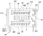
図4ないし図8を参照すれば、本発明の1つの好適な実施形態による電気コネクタは、絶縁ハウジング4と、第1の導電性端子モジュール5と、第2の導電性端子モジュール6と、2つの位置設定部分46とを備えている。絶縁ハウジング4は、プラスチック材料で形成され、本体41と、この本体41の上半分及び下半分に接続された2つの挿入部分42と、挿入ガイド部分43と、支持部分44と、少なくとも1つの接続部分45とを有し、この接続部分45は、ここに示す実施形態では、2つの接続部分45であるのが好ましい。Referring to FIGS. 4 to 8, an electrical connector according to one preferred embodiment of the present invention includes an insulating housing 4, a first
本体41は、相手コネクタを接続するための第1の面411と、この第1の面411とは逆の第2の面412と、長い本体41の端から延びる第1の端413と、この第1の端413に対して逆の端を形成するように延びる第2の端414と、第1の垂下プレート415と、第2の垂下プレート416とを有し、これら第1の垂下プレート415及び第2の垂下プレート416の両方は、互いに対向すると共に、第1の面411、第2の面412、第1の端413及び第2の端414によって画成される。組み立てのために、第2の垂下プレート416だけを回路板に向って設置することができる。本体41は、第1の面411から第2の面412へ貫通するように本体41の上半分及び下半分に2行に各々配列された複数の端子スルーホール417を有する。The
2つの挿入部分42は、第1の面411に接続され、第1の面411から外方に延びる。挿入部分42の各々は、接続平面421及びバック平面422を有し、接続平面421は、端子スルーホール417に各々対応する複数の端子受け入れ溝4211を有し、更に、接続平面421は、電気コネクタと相手コネクタとの不適切な嵌合を防止するためのブロック4212を備えている。バック平面422は、保持くぼみ4221を有する。The two
挿入ガイド部分43も、第1の面411に接続されて、第1の面411から外方に延びる。挿入ガイド部分43及び各挿入部分42は、それらの間にギャップを画成する。挿入ガイド部分43は、各挿入部分42に隣接した側にガイドくぼみ431を有する。同様に、支持部分44は、第2の端414に隣接した第1の面411に形成されて、第1の面411から外方に延びる。支持部分44及び挿入ガイド部分43は、本体41に対称的に配置される。The
更に、接続部分45は、第2の面412に接続され、そして本体41の第1の端413及び第2の端414に各々隣接して、接続部分45は、第2の面412から外方に延びる。接続部分45の各々は、回路板に接触するための下部プレート(図示せず)と、この下部プレートとは逆の上部プレート451と、回路板に配置された固定穴に対応して上部プレート451から下部プレートへ貫通する接続穴452とを有している。Further, the connecting
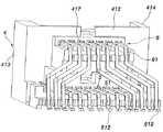
第1の導電性端子モジュール5は、複数の並置された第1導電性端子51を有し、各第1導電性端子51は、下方の挿入部分の端子受け入れ溝4211に各々しっかり収容された複数の第1コンタクト511と、端子スルーホール417を各々貫通するために2つの接続部分45間で第2の面412上を外方に突出する複数の第2コンタクト512とを有する。The first
第2の導電性端子モジュール6は、複数の並置された第2導電性端子61を有し、各第2導電性端子61は、上方の挿入部分42の端子受け入れ溝4211に各々しっかり収容された複数の第1コンタクト611と、端子スルーホール417を各々貫通するために2つの接続部分45間で第2の面412上を外方に突出する複数の第2コンタクト612とを有する。第1の導電性端子モジュール5の第1導電性端子51の各第2コンタクト512は、1つの行において第2の導電性端子モジュール6の第2導電性端子61の各第2コンタクト612と交互に配列される。The second
別の実施形態では、第1の導電性端子モジュール5の第1導電性端子51の第2コンタクト512は、第2の導電性端子モジュール6の第2導電性端子61の第2コンタクト612から離れて、互いに交互に食い違わされて又は2行において1対1の関係で(図9に示すように)配列される。In another embodiment, the
第3の実施形態では、第1の導電性端子モジュール5の第1導電性端子51の第2コンタクト512と、第2の導電性端子モジュール6の第2導電性端子61の第2コンタクト612を単一の行に配列して、第2の導電性端子モジュール6の第2導電性端子61の第2コンタクト612を2つのグループに分割しそして単一の行の両端に各々配列すると共に、第1の導電性端子モジュール5の第1導電性端子51の第2コンタクト512をそれらの間で単一の行の中間に配列することができる(図13及び図14を参照)。In the third embodiment, the
本体41は、第2の面412における下方位置に複数の第1突起418を各々有し、これらの第1突起418は、第1の導電性端子モジュール5の第1導電性端子51及び第2の導電性端子モジュール6の第2導電性端子61を各々分割しそして個々に位置設定する(図5に示すように)。別の実施形態では、第1突起418の各々は、第1の導電性端子モジュール5の第1導電性端子51のみを分割して位置設定するのに使用することができ(図9に示すように)、本体41は、更に、第2の面412における上方位置に複数の第2の突起419を備え、これら第2の突起419は、第2の導電性端子モジュール6の第2導電性端子61を各々分割して個々に位置設定する。The
ここに示す実施形態ではプレートロック部分を各々形成する位置設定部分46は、ストップストリップ461と、このストップストリップ461に対応する固定バックル462とを備えている。この固定バックル462は、2つの撓み変形可能なフック4621をその端に有し、これらフックは、互いに逆方向に外方に突出する。固定バックル462が上部プレート451から接続穴452を経て回路板の固定穴へと貫通する間に、各フック4621は、固定穴の対向リムにフック係合する。で は In the embodiment shown, the
回路板(図示せず)と組み立てるために、回路板は、第1導電性端子51及び第2導電性端子61に各々対応する複数の半田付けピンと、接続部分45の接続穴452に各々対応する複数の固定穴(図示せず)とを有し、絶縁ハウジング40の2つの接続部分45の下部プレートが回路板の表面に同時に電気的接続される。第1導電性端子51の第2コンタクト512及び第2導電性端子61の第2コンタクト612は、電気的接続のための表面取り付け技術により半田付けピン31に各々対応的に半田付けされる。固定バックル452が接続穴452を貫通して、フック4621により回路板の各固定穴に接続される。別の実施形態では、位置設定部分46も、表面取り付けデバイスの形式のもので(図13及び図14に示すように)、表面取り付け技術により回路板に取り付けられる。In order to assemble with a circuit board (not shown), the circuit board corresponds to a plurality of soldering pins respectively corresponding to the first
その後、ガイドくぼみ431及び保持くぼみ4221が、相手コネクタを挿入部分42へガイドして位置設定し、複数の相手コネクタは、回路板に接続するために第1導電性端子51の第1コンタクト511及び第2導電性端子61の第1コンタクト611に各々接触することにより電気的情報を転送する。Thereafter, the
従って、2つの位置設定部分46は、絶縁ハウジング40と回路板との間の相対的な位置を制限し、位置設定部分46は、相手コネクタを挿入接続する状態又は相手コネクタの挿入後に横方向の力が作用する状態において第1導電性端子51及び第2導電性端子61の荷重を分担するために著しい抵抗力を支持する。電気コネクタの標準化を想定して、第1導電性端子51及び第2導電性端子61の破壊により電気コネクタ1が故障するのを防止するために絶縁ハウジング40及び回路板の位置一致性能を改善することができる。別の実施形態では、位置設定部分46を位置設定極又は他の位置設定手段に置き換えることもできるし、或いは各位置設定部分46を各接続部分45と1部片で一体的に形成することもできる。Accordingly, the two
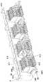
更に、上述した単一の電気コネクタは、2つ又はそれ以上の電気コネクタを組み合せて、4つ又はそれ以上の相手コネクタと挿入接続する複合コネクタとすることができる。図9及び10を参照すれば、4つの電気コネクタが組み合わされた複合コネクタの実施形態が示されており、1つのコネクタの本体41の第1の端413が、それに隣接する別のコネクタの本体41の第2の端414に接続され、この1つのコネクタ及び別のコネクタは、互いに結合されるか、又は一体的に形成される。この複合コネクタは、その両端において第1導電性端子モジュール6と第2導電性端子モジュール6との間に接続部分45を有する。この複合コネクタの位置設定部分46は、上記単一電気コネクタと同様であり、従って、その構成は、ここでは説明しない。Furthermore, the single electrical connector described above can be a composite connector that inserts and connects four or more mating connectors by combining two or more electrical connectors. Referring to FIGS. 9 and 10, there is shown an embodiment of a composite connector in which four electrical connectors are combined, wherein the
別の実施形態では、接続穴452は、上部プレート451を貫通せずに下部プレートからまっすぐに形成されたくぼみでもよく、更に、位置設定部分46は、接続部分45の接続穴452と挿入接続するものであれば、種々の構成でよい(図12に示すような)。In another embodiment, the connection holes 452 may be recesses formed straight from the lower plate without penetrating the
本発明は、回路板と共に挿入接続して電気的接続を与える複数の相手コネクタ、及び回路板の面積及び電気的装置の体積を維持して小型軽量の目標を達成するようにスタック形式で設計された電気コネクタを提供する。The present invention is designed with a plurality of mating connectors to provide an electrical connection by inserting and connecting with a circuit board, and in a stack format to achieve the goal of small size and light weight while maintaining the area of the circuit board and the volume of the electrical device. Provide an electrical connector.
以上、本発明の特定の実施形態を詳細に説明したが、これは、本発明を単に例示するものに過ぎず、それ故、特許請求の範囲内で種々の変更や修正がなされ得ることが当業者に明らかであろう。Although specific embodiments of the present invention have been described in detail, these are merely illustrative of the present invention, and thus various changes and modifications may be made within the scope of the appended claims. It will be clear to the trader.
4:絶縁ハウジング
5:第1導電性端子モジュール
6:第2導電性端子モジュール
41:本体
42:挿入部分
43:挿入ガイド部分
44:支持部分
45:接続部分
46:位置設定部分
51:第1導電性端子
61:第2導電性端子
411:第1の面
412:第2の面
413:第1の端
414:第2の端
415:第1の垂下プレート
416:第2の垂下プレート
417:端子スルーホール
418:第1突起
419:第2突起
421:接続平面
422:バック平面
431:ガイドくぼみ
452:接続穴
461:ストップストリップ
462:固定バックル
511:第1コンタクト
512:第2コンタクト
4211:端子受け入れ溝
4212:ブロック
4621:フック
4: Insulating housing 5: First conductive terminal module 6: Second conductive terminal module 41: Main body 42: Insertion part 43: Insertion guide part 44: Support part 45: Connection part 46: Position setting part 51: First conductive part Terminal 61: second conductive terminal 411: first surface 412: second surface 413: first end 414: second end 415: first hanging plate 416: second hanging plate 417: terminal Through hole 418: First protrusion 419: Second protrusion 421: Connection plane 422: Back plane 431: Guide recess 452: Connection hole 461: Stop strip 462: Fixed buckle 511: First contact 512: Second contact 4211: Terminal receiving Groove 4212: Block 4621: Hook
Claims (5)
Translated fromJapanese本体が形成され、該本体の上半分と下半分に2つの挿入部分が各々配置されている絶縁ハウジングを備え、
上記本体は、第1の面と、該第1の面とは逆の第2の面とを有し、上記挿入部分は、上記第1の面から、上記第2の面から離れる方向に延びており、
上記本体の上記下半分の上記挿入部分は、導電性端子の第1セットを含むと共に、上記上半分の上記挿入部分は、導電性端子の第2セットを備え、各々の導電性端子は、第1コンタクト及び第2コンタクトを有し、上記第1コンタクトは、上記本体の上記第1の面から、上記第2の面から離れる方向に延び、更に、上記第2コンタクトは、上記第2の面から、上記第1の面から離れる方向に突出し、そして
上記本体は、上記第2の面における下方位置に複数の第1突起を各々有し、該第1突起は、上記第1セットの導電性端子の上記第2コンタクトを各々分割して個々に位置設定するものである電気コネクタ。An electrical connector attached to a circuit board for insertion connection to two mating connectors,
A body formed and an insulating housing in which two inserts are respectively located in the upper and lower halves of the body;
The body has a first surface and a second surface opposite to the first surface, and the insertion portion extends from the first surface in a direction away from the second surface. And
The insertion portion of the lower half of the body includes a first set of conductive terminals, and the insertion portion of the upper half includes a second set of conductive terminals, each conductive terminal having a second set of conductive terminals. A first contact extending from the first surface of the main body in a direction away from the second surface; and a second contact extending from the second surface to the second surface. Projecting away from the first surface from the first surface, and the body has a plurality of first protrusions each at a lower position on the second surface, the first protrusions being the first set of conductive members. An electric connector, wherein the second contacts of the terminals are divided and individually positioned.
The second contact of the second conductive terminal is divided into two groups, and the second contact of the first conductive terminal is connected to two of the second contact of the second set of conductive terminals. The electrical connector of claim 1 arranged between groups.
Applications Claiming Priority (1)
| Application Number | Priority Date | Filing Date | Title |
|---|---|---|---|
| TW091213679UTW543962U (en) | 2002-08-30 | 2002-08-30 | Electrical connector |
Publications (1)
| Publication Number | Publication Date |
|---|---|
| JP2004134401Atrue JP2004134401A (en) | 2004-04-30 |
Family
ID=29708866
Family Applications (1)
| Application Number | Title | Priority Date | Filing Date |
|---|---|---|---|
| JP2003345027APendingJP2004134401A (en) | 2002-08-30 | 2003-08-27 | Electrical connector |
Country Status (3)
| Country | Link |
|---|---|
| US (1) | US6811433B2 (en) |
| JP (1) | JP2004134401A (en) |
| TW (1) | TW543962U (en) |
Cited By (1)
| Publication number | Priority date | Publication date | Assignee | Title |
|---|---|---|---|---|
| KR101383444B1 (en)* | 2012-05-18 | 2014-04-08 | 주식회사 후성테크 | Dual electric connector |
Families Citing this family (17)
| Publication number | Priority date | Publication date | Assignee | Title |
|---|---|---|---|---|
| TW576559U (en)* | 2003-06-27 | 2004-02-11 | Hon Hai Prec Ind Co Ltd | Electrical connector |
| TWM249239U (en)* | 2003-07-30 | 2004-11-01 | Hon Hai Prec Ind Co Ltd | Electrical connector |
| EP1643597B1 (en)* | 2004-09-29 | 2007-11-28 | Sumitomo Wiring Systems, Ltd. | A connector and terminal fitting |
| US7361060B2 (en)* | 2005-08-04 | 2008-04-22 | Illinois Tool Works Inc | Connector with bifurcated conductor |
| CN2840358Y (en)* | 2005-09-28 | 2006-11-22 | 富士康(昆山)电脑接插件有限公司 | Electric connector |
| CN201000941Y (en)* | 2006-12-18 | 2008-01-02 | 富士康(昆山)电脑接插件有限公司 | Electrical connector |
| CN101295841B (en)* | 2007-04-24 | 2012-06-27 | 莫列斯公司 | Electric connector combination system |
| CN201072836Y (en)* | 2007-06-15 | 2008-06-11 | 富士康(昆山)电脑接插件有限公司 | Electrical connector |
| JP5038818B2 (en) | 2007-08-22 | 2012-10-03 | 株式会社オートネットワーク技術研究所 | Board connector |
| US7850490B2 (en)* | 2007-12-13 | 2010-12-14 | Ati Technologies Ulc | Electrical connector, cable and apparatus utilizing same |
| US7861013B2 (en)* | 2007-12-13 | 2010-12-28 | Ati Technologies Ulc | Display system with frame reuse using divided multi-connector element differential bus connector |
| US8137127B2 (en)* | 2007-12-13 | 2012-03-20 | Ati Technologies Ulc | Electronic devices using divided multi-connector element differential bus connector |
| CN101626117B (en)* | 2008-07-08 | 2012-08-29 | 鸿富锦精密工业(深圳)有限公司 | Electrical connection structure |
| DE102011003036A1 (en)* | 2011-01-24 | 2012-07-26 | Tyco Electronics Amp Gmbh | Electrical plug connector for electrically connecting e.g. electrical circuit of infotainment system of motor car with plug connector counterparts, to transmit data signals, has socket apertures separated from each other by partition wall |
| CN202183478U (en)* | 2011-08-11 | 2012-04-04 | 番禺得意精密电子工业有限公司 | Electric connector |
| CN104701677A (en)* | 2013-12-10 | 2015-06-10 | 富士康(昆山)电脑接插件有限公司 | Electric connector |
| US9899780B2 (en)* | 2015-07-15 | 2018-02-20 | Alan L. Pocrass | RJ and USB connectors with grooved contact pins |
Family Cites Families (9)
| Publication number | Priority date | Publication date | Assignee | Title |
|---|---|---|---|---|
| US4818239A (en)* | 1987-04-24 | 1989-04-04 | Maxconn, Inc. | Stacked multipin connectors |
| US4857017A (en)* | 1987-04-24 | 1989-08-15 | Maxconn, Inc. | Support device for wires in multi-contact connectors |
| US5080596A (en)* | 1990-11-30 | 1992-01-14 | Amp Incorporated | Connector with contact spacer plate providing greater lateral force on rear contacts |
| US5037330A (en)* | 1990-11-30 | 1991-08-06 | Amp Corporated | Stacked circular DIN connector |
| US5336109A (en)* | 1993-04-15 | 1994-08-09 | The Whitaker Corporation | Stacked connector assembly |
| US6200161B1 (en)* | 1998-04-03 | 2001-03-13 | The Whitaker Corporation | Stacked electrical connector |
| TW395596U (en)* | 1998-09-04 | 2000-06-21 | Hon Hai Prec Ind Co Ltd | Connector assembly |
| TW383957U (en)* | 1998-11-03 | 2000-03-01 | Hon Hai Prec Ind Co Ltd | Combination of electrical connector |
| US6350152B1 (en)* | 2000-08-23 | 2002-02-26 | Berg Technology Inc. | Stacked electrical connector for use with a filter insert |
- 2002
- 2002-08-30TWTW091213679Upatent/TW543962U/ennot_activeIP Right Cessation
- 2003
- 2003-08-27JPJP2003345027Apatent/JP2004134401A/enactivePending
- 2003-08-28USUS10/650,175patent/US6811433B2/ennot_activeExpired - Fee Related
Cited By (1)
| Publication number | Priority date | Publication date | Assignee | Title |
|---|---|---|---|---|
| KR101383444B1 (en)* | 2012-05-18 | 2014-04-08 | 주식회사 후성테크 | Dual electric connector |
Also Published As
| Publication number | Publication date |
|---|---|
| US20040115969A1 (en) | 2004-06-17 |
| US6811433B2 (en) | 2004-11-02 |
| TW543962U (en) | 2003-07-21 |
Similar Documents
| Publication | Publication Date | Title |
|---|---|---|
| JP2004134401A (en) | Electrical connector | |
| US6848950B2 (en) | Multi-interface power contact and electrical connector including same | |
| US8292635B2 (en) | Connector assembly with robust latching means | |
| US9735526B1 (en) | Hybrid socket connector integrated with power supply and signal transmission functions | |
| US7351091B1 (en) | Header connector | |
| US7588443B2 (en) | Board-to-board electrical connector assembly | |
| US7972171B2 (en) | Card edge connector | |
| US4938719A (en) | Junction block | |
| US7578696B2 (en) | Electrical connector with cover configured for heat dissipation | |
| US4384754A (en) | Multi-plane connectors | |
| US20080214060A1 (en) | Electrical connector having improved based element | |
| WO2005011060A3 (en) | Electrical interconnect assembly with interlocking contact system | |
| US7175447B2 (en) | Backplane connector | |
| JP2009520325A (en) | Electrical connector assembly and manufacturing method thereof | |
| JPH03226976A (en) | Electric connector and contact for use with electric connector | |
| US7234951B2 (en) | Electrical connector with protective cover for post header | |
| US6652317B2 (en) | Electrical connector | |
| US6755671B1 (en) | Electrical connector having improved ground structure | |
| TW531944B (en) | Board mount type connector and board mounting structure of connector | |
| JPH05258811A (en) | Printed circuit board and outrigger edge connector assembly and assembling thereof | |
| US6068509A (en) | Stacking type connector | |
| US7083433B2 (en) | Electrical connector | |
| US7004763B2 (en) | Board-to-board electrical connector assembly | |
| US6220868B1 (en) | Card edge connector | |
| JPH0361996B2 (en) |
Legal Events
| Date | Code | Title | Description |
|---|---|---|---|
| A977 | Report on retrieval | Free format text:JAPANESE INTERMEDIATE CODE: A971007 Effective date:20060720 | |
| A131 | Notification of reasons for refusal | Free format text:JAPANESE INTERMEDIATE CODE: A131 Effective date:20060801 | |
| A601 | Written request for extension of time | Free format text:JAPANESE INTERMEDIATE CODE: A601 Effective date:20061023 | |
| A602 | Written permission of extension of time | Free format text:JAPANESE INTERMEDIATE CODE: A602 Effective date:20061026 | |
| A521 | Request for written amendment filed | Free format text:JAPANESE INTERMEDIATE CODE: A523 Effective date:20061101 | |
| A02 | Decision of refusal | Free format text:JAPANESE INTERMEDIATE CODE: A02 Effective date:20070410 |