JP2004133719A - Microcomputer - Google Patents
MicrocomputerDownload PDFInfo
- Publication number
- JP2004133719A JP2004133719AJP2002298189AJP2002298189AJP2004133719AJP 2004133719 AJP2004133719 AJP 2004133719AJP 2002298189 AJP2002298189 AJP 2002298189AJP 2002298189 AJP2002298189 AJP 2002298189AJP 2004133719 AJP2004133719 AJP 2004133719A
- Authority
- JP
- Japan
- Prior art keywords
- timer
- control
- clock
- bit
- signal
- Prior art date
- Legal status (The legal status is an assumption and is not a legal conclusion. Google has not performed a legal analysis and makes no representation as to the accuracy of the status listed.)
- Pending
Links
Images


Classifications
- G—PHYSICS
- G06—COMPUTING OR CALCULATING; COUNTING
- G06F—ELECTRIC DIGITAL DATA PROCESSING
- G06F1/00—Details not covered by groups G06F3/00 - G06F13/00 and G06F21/00
- G06F1/04—Generating or distributing clock signals or signals derived directly therefrom
- G06F1/14—Time supervision arrangements, e.g. real time clock
- G—PHYSICS
- G06—COMPUTING OR CALCULATING; COUNTING
- G06F—ELECTRIC DIGITAL DATA PROCESSING
- G06F1/00—Details not covered by groups G06F3/00 - G06F13/00 and G06F21/00
- G06F1/16—Constructional details or arrangements
- G06F1/20—Cooling means
- G06F1/206—Cooling means comprising thermal management
Landscapes
- Engineering & Computer Science (AREA)
- Theoretical Computer Science (AREA)
- Physics & Mathematics (AREA)
- General Engineering & Computer Science (AREA)
- General Physics & Mathematics (AREA)
- Human Computer Interaction (AREA)
- Liquid Crystal Display Device Control (AREA)
- Microcomputers (AREA)
Abstract
Description
Translated fromJapanese【0001】
【発明の属する技術分野】
本発明は、マイクロコンピュータに関し、特に1つのチップ上に形成されたマイクロコンピュータ、いわゆるワンチップマイクロコンピュータにおいて、冷却装置の制御および表示装置の輝度制御に好適なマイクロコンピュータに適用して有効な技術に関する。
【0002】
【従来の技術】
本発明者が検討したところによれば、マイクロコンピュータに関しては、以下のような技術が考えられる。
【0003】
たとえば、マイクロコンピュータの一例として、ノート型パーソナルコンピュータに用いられるワンチップマイクロコンピュータは、演算処理を行うCPU(Central Processing Unit)、クロック信号を発生するCPG(Clock Pulse Generator)、制御プログラムなどを記憶するフラッシュメモリ、データなどを記憶するRAM(Random Access Memory)、冷却用ファンやLCD(Liquid Crystal Display)などの周辺装置を制御するアナログ回路(A−D(Analog−Digital)回路,D−A(Digital−Analog)回路)、外部と接続するI/O(Input/Output)回路、バスインタフェースなどから構成され、これらが1つのチップ上に形成されている。
【0004】
また、このようなマイクロコンピュータにおいては、たとえばLCDのバックライト電源を制御するために、HighとLowの期間を可変して所望の電圧を生成するPWM(Pulse Width Modulation)回路をワンチップ内に搭載した液晶表示用のマイクロコンピュータの技術がある(例えば、特許文献1参照)。
【0005】
【特許文献1】
特開平9−6934号公報
【0006】
【発明が解決しようとする課題】
ところで、前記のようなマイクロコンピュータについて、本発明者が検討した結果、以下のようなことが明らかとなった。
【0007】
たとえば、前述のように、ファンやLCDなどの周辺装置をアナログ回路で制御するワンチップマイクロコンピュータでは、アナログ回路を搭載する必要があり、これによってチップサイズの増大を招き、また基板実装、チップレイアウトの際にアナログ専用電源を搭載しなければならない。この結果、このチップサイズの増大、アナログ専用電源の搭載は、ワンチップマイクロコンピュータのコストアップにもつながる。
【0008】
また、前記特許文献1の技術でも、LCDの制御はPWM回路で可能となるものの、同じワンチップマイクロコンピュータによりファンを制御する場合には、このファンを制御する回路が必要となるが、ファンを制御することまでは考慮されていない。
【0009】
そこで、本発明の目的は、チップサイズの増大およびアナログ専用電源の搭載が必要なアナログ回路を搭載することなく、冷却装置の制御および表示装置の輝度制御、さらにはバッテリの充放電制御を実現することができるワンチップマイクロコンピュータを提供することにある。
【0010】
本発明の前記ならびにその他の目的と新規な特徴は、本明細書の記述および添付図面から明らかになるであろう。
【0011】
【課題を解決するための手段】
本願において開示される発明のうち、代表的なものの概要を簡単に説明すれば、次のとおりである。
【0012】
すなわち、本発明は、ワンチップマイクロコンピュータに適用され、冷却装置を制御するために使用可能な低分解能タイマと、表示装置の輝度を調整するために使用可能な高分解能タイマとを含むものである。これにより、低分解能タイマによって冷却装置を制御し、高分解能タイマによって表示装置の輝度を調整することができる。よって、アナログ回路を搭載する必要がないので、アナログ専用電源を必要としないため、チップサイズの低減、システムの簡素化が実現できるようになる。
【0013】
このワンチップマイクロコンピュータにおいては、さらに高分解能タイマをバッテリの充放電を制御するために使用可能とするものである。また、低分解能タイマが低周波出力、高分解能タイマが高周波出力とし、これらの低周波、高周波を基準のクロック信号を分周して生成するようにしたものである。また、高分解能タイマは、PWM回路を有するものである。
【0014】
【発明の実施の形態】
以下、本発明の実施の形態を図面に基づいて詳細に説明する。なお、実施の形態を説明するための全図において、同一機能を有する部材には同一の符号を付し、その繰り返しの説明は省略する。
【0015】
図1により、本発明の一実施の形態のワンチップマイクロコンピュータを使用したノート型パーソナルコンピュータの構成の一例を説明する。図1はワンチップマイクロコンピュータを使用したノート型パーソナルコンピュータのブロック図を示す。
【0016】
本実施の形態のワンチップマイクロコンピュータを使用したノート型パーソナルコンピュータは、たとえば全体の演算処理を行うCPU1と、相互のデータ転送を制御するノースブリッジ2およびサウスブリッジ3と、周辺装置を制御するワンチップマイクロコンピュータ4と、制御プログラム(システムBIOS(Basic Input Output System)など)などを記憶するフラッシュメモリ5と、冷却装置である2つのファン6,7と、表示装置であるLCDの輝度制御を行うLCD輝度コントローラ8と、電源となる2つのバッテリ9,10と、バッテリ9,10を切り替えるバッテリセレクタ11と、バッテリ9,10を充電する電圧チャージャ12と、入力装置であるキーボード13およびマウス14と、キーボード13の打鍵変換を行うキーマトリクス15と、温度およびファンの回転を監視する温度・ファンモニタIC16と、電力を監視する電力モニタIC17などから構成される。
【0017】
ワンチップマイクロコンピュータ4は、演算処理を行うCPU21と、クロック信号を発生するCPG22と、制御プログラム(ACPI(AdvancedConfiguration and Power Interface)ファームウェアなど)などを記憶するフラッシュメモリ23と、データなどを記憶するRAM24と、ファン6,7を制御する8ビットタイマ25と、LCD輝度コントローラ8および電圧チャージャ12を制御する14ビットタイマ26と、バッテリ9,10およびバッテリセレクタ11を制御するバッテリコントローラ27,28と、キーボード13およびマウス14を制御するキーボードコントローラ29と、キーマトリクス15と接続するI/O回路30と、ノースブリッジ2およびサウスブリッジ3を介してCPU1と接続するLPCバスとのバスインタフェース31などから構成される。このワンチップマイクロコンピュータ4は、公知の半導体製造技術により1つのチップ上に形成されている。
【0018】
次に、図2により、ワンチップマイクロコンピュータにおいて、CPGと8ビットタイマおよび14ビットタイマの構成の一例を説明する。図2はCPGと8ビットタイマおよび14ビットタイマのブロック図を示す。
【0019】
CPG22は、クロック信号EXTAL,XTALを入力とする発振器41と、この発振器41から出力されたクロック信号をデューティ補正するデューティ補正回路42と、別系統で低周波クロック信号EXCLを入力とする発振器43と、デューティ補正回路42から出力されたクロック信号と発振器43から出力されたクロック信号のいずれかを選択するクロック選択回路44と、このクロック選択回路44から出力されたクロック信号Φを分周する分周器45と、この分周器45から出力されたクロック信号Φ/2〜Φ/32とクロック選択回路44から出力されたクロック信号Φのいずれかを選択するバスマスタクロック選択回路46などから構成される。
【0020】
このCPG22において、バスマスタクロック選択回路46から出力されたクロック信号はCPU21やDTCなどに供給されて、このCPU21やDTCなどはバスマスタクロック信号に同期して動作する。また、クロック選択回路44から出力されたクロック信号Φは、8ビットタイマ25、14ビットタイマ26などにそれぞれ供給され、このクロック信号Φが基準となっている。
【0021】
8ビットタイマ25は、詳細は後述するが、CPG22のクロック選択回路44から出力されたクロック信号Φを入力として、この基準となるクロック信号Φを分周する分周器51と、この分周器51により分周されたクロック信号を演算処理するコントロールロジック回路52などから構成され、このコントロールロジック回路52から低周波の信号が出力される。
【0022】
14ビットタイマ26は、詳細は後述するが、CPG22のクロック選択回路44から出力されたクロック信号Φを入力として、この基準となるクロック信号Φを分周する分周器61と、この分周器61により分周されたクロック信号をパルス幅変換処理するコントロールロジック回路62などから構成され、このコントロールロジック回路62から高周波の信号が出力される。
【0023】
次に、図3〜図6により、8ビットタイマの構成および動作の一例を詳細に説明する。図3は8ビットタイマのブロック図、図4はタイマコントロールレジスタ、タイマコントロール/ステータスレジスタの設定(チャンネル1)、図5はタイマコントロールレジスタ、タイマコントロール/ステータスレジスタの設定(チャンネル2)、図6は8ビットタイマにより生成される信号の波形図をそれぞれ示す。
【0024】
8ビットタイマ25は、冷却装置のファン6,7を制御するために使用可能な低分解能のタイマであり、たとえば図3に一例を示すように、前述した分周器51およびコントロールロジック回路52と、クロック選択回路53、タイマコントロールレジスタTCRX(チャンネル1),TCRY(チャンネル2)、タイマコントロール/ステータスレジスタTCSRなどから構成される。
【0025】
分周器51は、内部クロック信号Φを入力として、この内部クロック信号Φを分周し、分周されたクロック信号Φ/2,Φ/4,Φ/256,Φ/2048を生成する。クロック選択回路53は、内部クロック信号Φ、分周器51により分周されたクロック信号Φ/2,Φ/4,Φ/256,Φ/2048、外部クロック信号の中から所望のクロック信号を選択する。この選択制御信号は、コントロールロジック回路52から供給される。
【0026】
コントロールロジック回路52は、クロック選択回路53により選択されたクロック信号に同期し、タイマコントロールレジスタTCRX,TCRY、タイマコントロール/ステータスレジスタTCSRに設定されたデータに基づいて演算処理し、チャンネル1のファン6のモータを制御する出力信号TMOX、チャンネル2のファン7のモータを制御する出力信号TMOYをそれぞれ生成する。また、コントロールロジック回路52には、外部のリセット信号などからレジスタリセット信号TMRIX,TMRIYが入力され、各レジスタが初期化される。
【0027】
チャンネル1側のタイマコントロールレジスタTCRX、タイマコントロール/ステータスレジスタTCSRの設定の一例は、たとえば図4に示すように、TCRX(ビット5)、TCSR(ビット2)、TCSR(ビット1)、TCSR(ビット0)にそれぞれ、1000の設定でクロック入力禁止、1001の設定でΦ/2048でカウント、1010の設定でΦ/4096でカウント、1011の設定でΦ/8192でカウント、1100の設定でコンペアマッチでカウント、などが可能となる。すなわち、このチャンネル1の設定例では、Φ/2048、Φ/4096、Φ/8192による3種類の制御が可能となっている。
【0028】
チャンネル2側のタイマコントロールレジスタTCRY、タイマコントロール/ステータスレジスタTCSRの設定の一例は、たとえば図5に示すように、TCRY(ビット4)、TCSR(ビット2)、TCSR(ビット1)、TCSR(ビット0)にそれぞれ、1000の設定でクロック入力禁止、1001の設定でΦ/4096でカウント、1010の設定でΦ/8192でカウント、1011の設定でΦ/16384でカウント、1100の設定でオーバーフローでカウント、などが可能となる。すなわち、このチャンネル2の設定例では、Φ/4096、Φ/8192、Φ/16384による3種類の制御が可能となっている。
【0029】
以上のように設定される8ビットタイマ25においては、たとえば図6に一例を示すように、基準のクロック信号(内部クロック信号)Φをもとに、この基準のクロック信号Φを分周器51により分周し、この分周したクロック信号、内部クロック信号Φ、外部クロック信号の中でクロック選択回路53から選択された信号からコントロールロジック回路52によりコンペアマッチ信号を生成し、このコンペアマッチ信号に基づいて低周波の信号を生成し、この信号を出力信号として出力する。たとえば一例として、この8ビットタイマ25では、30〜60Hz程度の周波数の信号が生成される。ここで、コンペアマッチ信号とはTCSR,TCRX,TCRYにて定めた制御クロックによりコントロールロジック回路52で生成され、その波形を使用して信号の出力を行っている。
【0030】
この8ビットタイマ25は、前述のように出力が2チャンネル分搭載されており、一方の出力信号は一方のファン6に供給し、他方の出力信号は他方のファン7に供給し、これによって各ファン6,7の駆動をそれぞれ独立に制御することができる。
【0031】
次に、図7〜図13により、14ビットタイマの構成および動作の一例を詳細に説明する。図7は14ビットタイマのブロック図、図8は周辺クロックセレクトレジスタの設定、図9はクロックセレクト、図10はPWMデータレジスタの設定、図11は出力波形の設定、図12は14ビットタイマにより生成される信号の波形図をそれぞれ示す。
【0032】
14ビットタイマ26は、表示装置のLCDの輝度を調整するために使用可能な高分解能のタイマであり、たとえば図7に一例を示すように、前述した分周器61およびコントロールロジック回路62と、クロック選択回路63、周辺クロックセレクトレジスタPCSR、PWMデータレジスタDADRA(チャンネル1),DADRB(チャンネル2)、内部カウントレジスタDACNT、PWMコントロールレジスタDACRなどから構成される。
【0033】
分周器61は、内部クロック信号Φを入力として、この内部クロック信号Φを分周し、分周されたクロック信号Φ/2,Φ/64,Φ/128,Φ/256,Φ/1024,Φ/4096,Φ/16384を生成する。クロック選択回路63は、内部クロック信号Φ、分周器61により分周されたクロック信号Φ/2,Φ/64,Φ/128,Φ/256,Φ/1024,Φ/4096,Φ/16384の中から、CPU21から周辺クロックセレクトレジスタPCSRに設定されたデータに基づいて所望のクロック信号を選択する。この選択制御信号は、コントロールロジック回路62から供給される。
【0034】
コントロールロジック回路62は、クロック選択回路63により選択されたクロック信号に同期し、PWMデータレジスタDADRA,DADRB、内部カウントレジスタDACNT、PWMコントロールレジスタDACRに設定されたデータに基づいてパルス幅変換処理し、チャンネル1のLCDのLCD輝度コントローラ8を制御する出力信号PWX0、チャンネル2のバッテリ9,10の電圧チャージャ12を制御する出力信号PWX1をそれぞれ生成する。
【0035】
周辺クロックセレクトレジスタPCSRの設定の一例は、たとえば図8に示すように、ビット7(PWCKX1B)でPWMX_1クロックセレクト、ビット6(PWCKX1A)でPWMX_1のDACRのCKSが1の状態でクロックを選択(後述する図9参照)、ビット5(PWCKX0B)でPWMX_0クロックセレクト、ビット4(PWCKX0A)でPWMX_0のDACRのCKSが1の状態でクロックを選択(図9参照)、ビット3(PWCKX1C)でPWMX_1クロックセレクト、かつPWMX_1のDACRのCKSが1の状態でクロックを選択(図9参照)、ビット0(PWCKX0C)でPWMX_0クロックセレクト、かつPWMX_0のDACRのCKSが1の状態でクロックを選択(図9参照)、などが可能となる。
【0036】
PWMX_1,PWMX_0クロックセレクトの一例は、たとえば図9に示すように、PWCKX0C/PWCKX1C、PWCKX0B/PWCKX1B、PWCKX0A/PWCKX1Aにそれぞれ、000の設定で分解能(T)がシステムクロック周期×2で動作、001の設定でシステムクロック周期×64で動作、以降同様に、010で×128、011で×256、100で×1024、101で×4096、110で×16384、となり、111の設定で設定禁止、などが可能となる。すなわち、この設定例では、システムクロック周期それ自体と併せて8種類の分解能による制御が可能となっている。分解能とは、DADRA,DADRBでHigh幅、Low幅を設定する際に基準となる時間である。
【0037】
PWMデータレジスタDADRA,DADRBの設定の一例は、たとえば図10に示すように、ビット15〜ビット2(DA13〜DA0)で出力波形の設定(後述する図11参照)が可能であり、ビット1(CFS)でR/Wキャリアフリーケンシセレクトにより、0の設定で基本周期=分解能(T)×64で動作し、DA13〜DA0の値の範囲はH’0100〜H’3FFF、1の設定で基本周期=分解能(T)×256で動作し、DA13〜DA0の値の範囲はH’0040〜H’3FFF、などが可能となる。
【0038】
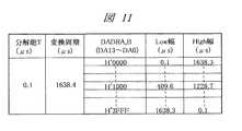
出力波形の設定の一例(φ:10MHz、内部クロックΦの例)は、たとえば図11に示すように、分解能(T)=0.1μs、変換周期=1638.4μsの場合に、PWMデータレジスタDADRA,DADRB(DA13〜DA0)がH’0000の設定でLow幅は0.1μs、High幅は1638.3μs、…、H’1000の設定でLow幅は409.6μs、High幅は1228.7μs、…、H’3FFFの設定でLow幅は1638.3μs、High幅は0.1、となる。
【0039】
以上のように設定される14ビットタイマ26においては、基準のクロック信号Φをもとに、この基準のクロック信号Φを分周器61により分周し、この分周したクロック信号からコントロールロジック回路62により所望のデューティ比による高周波の信号を生成し、このデューティ比の信号を出力信号として出力する。たとえば一例として、この14ビットタイマ26では、LCDの輝度調整に270〜280Hz程度の周波数のクロック信号が生成される。
【0040】
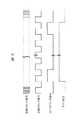
この14ビットタイマ26による出力波形は、たとえば図12に一例を示すように、1変換周期(分解能(T)×214)中に発生するパルス(CFS=0の場合は64、CFS=1の場合は256)の0レベル幅(Low幅:tL)の合計(TL)がPWMデータレジスタDADRA,DADRBのDA13〜DA0の値と対応する。OS=0の場合、この波形が直接出力される。OS=1の場合、この波形が反転して出力される。OS=1の時、1レベル幅(High幅:tH)の合計(TH)がPWMデータレジスタDADRA,DADRBのDA13〜DA0の値と対応する。また、PWMタイマは14bit変換精度を持っているため、分解能×214の周期でH/Lの変換を行っている。なお、この14ビットタイマ26における基準クロック信号(内部クロック信号)、分周クロック信号については、前述した図6とほぼ同様である。
【0041】
以上説明した例では、2種類の基本周期と8種類の分解能との組み合わせにより、16種類の波形を選択して生成できる。2種類の基本周期は、分解能(T)×64、分解能(T)×256、である。8種類の分解能は、システムクロック周期、システムクロック周期×2,×64,×128,×256,×1024,×4096,×16384、である。
【0042】
この14ビットタイマ26から出力された所望のデューティ比の信号は、LCD輝度コントローラ8において、コンデンサ、抵抗などからなる平滑回路により平滑化してアナログ電圧(図12に破線で表示)を生成し、このアナログ電圧によりLCDの輝度を調整することができる。たとえば、デューティ比を可変してHighの期間を短くすることで低い電圧を作ることができ、この低電圧は低消費電力化が必要なノート型パーソナルコンピュータに有効となる。
【0043】
また、この14ビットタイマ26は、出力が2チャンネル分搭載されており、一方の出力信号は前述のようにLCDの輝度調整に使用され、他方の出力信号はバッテリ9,10の充放電を制御するために使用される。バッテリ9,10の充放電を制御する場合にも、LCDの輝度を調整する場合と同様に、所望のデューティ比の信号によりバッテリ9,10の充電および放電を制御することができる。このLCDの輝度調整とバッテリの充放電制御は、チャンネル毎にそれぞれ独立に制御することができる。
【0044】
従って、本実施の形態によれば、8ビットタイマ25によって低周波による低速なクロック信号を生成できるので、ファン6,7のモータを直接制御することができる。また、14ビットタイマ26によって所望のデューティ比のクロック信号を生成することができるので、このクロック信号を平滑化したアナログ電圧によってLCDの制御およびバッテリ9,10の制御を行うことができる。
【0045】
この結果、ワンチップマイクロコンピュータ4からアナログ回路を削除したことにより、アナログ専用電源を必要としないため、ワンチップマイクロコンピュータ4のチップサイズを低減し、さらにこのワンチップマイクロコンピュータ4を搭載したノート型パーソナルコンピュータを簡素化することができる。
【0046】
以上、本発明者によってなされた発明をその実施の形態に基づき具体的に説明したが、本発明は前記実施の形態に限定されるものではなく、その要旨を逸脱しない範囲で種々変更可能であることはいうまでもない。
【0047】
たとえば、前記実施の形態においては、ワンチップマイクロコンピュータからアナログ回路を削除したことによる効果を得ることを目的としたが、アナログ回路を搭載した場合には、このアナログ回路による処理によって温度およびファンの回転を監視する機能や、電力を監視する機能を搭載することができるので、ワンチップマイクロコンピュータの高機能化を実現することができる。
【0048】
【発明の効果】
本願において開示される発明のうち、代表的なものによって得られる効果を簡単に説明すれば、以下のとおりである。
【0049】
(1)ワンチップマイクロコンピュータに、冷却装置を制御するために使用可能な低分解能タイマと、表示装置の輝度を調整するために使用可能な高分解能タイマとを搭載することで、低分解能タイマによって冷却装置を制御し、高分解能タイマによって表示装置の輝度を調整することができるので、アナログ回路を搭載する必要がなく、アナログ専用電源を必要としないため、ワンチップマイクロコンピュータのチップサイズの低減、およびこのワンチップマイクロコンピュータを用いたシステムの簡素化を実現することが可能となる。
【0050】
(2)ワンチップマイクロコンピュータにおいて、さらに高分解能タイマをバッテリの充放電を制御するために使用可能とすることで、より一層、チップサイズの低減およびシステムの簡素化を実現することが可能となる。
【図面の簡単な説明】
【図1】本発明の一実施の形態のワンチップマイクロコンピュータを使用したノート型パーソナルコンピュータを示すブロック図である。
【図2】本発明の一実施の形態のワンチップマイクロコンピュータにおいて、CPGと8ビットタイマおよび14ビットタイマを示すブロック図である。
【図3】本発明の一実施の形態のワンチップマイクロコンピュータにおいて、8ビットタイマを示すブロック図である。
【図4】本発明の一実施の形態のワンチップマイクロコンピュータにおける8ビットタイマにおいて、タイマコントロールレジスタ、タイマコントロール/ステータスレジスタの設定(チャンネル1)を示す説明図である。
【図5】本発明の一実施の形態のワンチップマイクロコンピュータにおける8ビットタイマにおいて、タイマコントロールレジスタ、タイマコントロール/ステータスレジスタの設定(チャンネル2)を示す説明図である。
【図6】本発明の一実施の形態のワンチップマイクロコンピュータにおいて、8ビットタイマにより生成される信号を示す波形図である。
【図7】本発明の一実施の形態のワンチップマイクロコンピュータにおいて、14ビットタイマを示すブロック図である。
【図8】本発明の一実施の形態のワンチップマイクロコンピュータにおける14ビットタイマにおいて、周辺クロックセレクトレジスタの設定を示す説明図である。
【図9】本発明の一実施の形態のワンチップマイクロコンピュータにおける14ビットタイマにおいて、クロックセレクトを示す説明図である。
【図10】本発明の一実施の形態のワンチップマイクロコンピュータにおける14ビットタイマにおいて、PWMデータレジスタの設定を示す説明図である。
【図11】本発明の一実施の形態のワンチップマイクロコンピュータにおける14ビットタイマにおいて、出力波形の設定を示す説明図である。
【図12】本発明の一実施の形態のワンチップマイクロコンピュータにおいて、14ビットタイマにより生成される信号を示す波形図である。
【符号の説明】
1 CPU
2 ノースブリッジ
3 サウスブリッジ
4 ワンチップマイクロコンピュータ
5 フラッシュメモリ
6,7 ファン
8 LCD輝度コントローラ
9,10 バッテリ
11 バッテリセレクタ
12 電圧チャージャ
13 キーボード
14 マウス
15 キーマトリクス
16 温度・ファンモニタIC
17 電力モニタIC
21 CPU
22 CPG
23 フラッシュメモリ
24 RAM
25 8ビットタイマ
26 14ビットタイマ
27,28 バッテリコントローラ
29 キーボードコントローラ
30 I/O回路
31 バスインタフェース
41,43 発振器
42 デューティ補正回路
44 クロック選択回路
45 分周器
46 バスマスタクロック選択回路
51,61 分周器
52,62 コントロールロジック回路
53,63 クロック選択回路[0001]
TECHNICAL FIELD OF THE INVENTION
The present invention relates to a microcomputer, and more particularly to a technique which is effective when applied to a microcomputer formed on one chip, that is, a so-called one-chip microcomputer, which is suitable for controlling a cooling device and controlling brightness of a display device. .
[0002]
[Prior art]
According to the study by the present inventor, the following techniques can be considered for microcomputers.
[0003]
For example, as an example of a microcomputer, a one-chip microcomputer used in a notebook personal computer stores a CPU (Central Processing Unit) that performs arithmetic processing, a CPG (Clock Pulse Generator) that generates a clock signal, a control program, and the like. A flash memory, a random access memory (RAM) for storing data, an analog circuit (A-D (Analog-Digital) circuit, a D-A (Digital) circuit for controlling peripheral devices such as a cooling fan and an LCD (Liquid Crystal Display). -Analog) circuit, an I / O (Input / Output) circuit connected to the outside, a bus interface, and the like. There are formed on one chip.
[0004]
In such a microcomputer, for example, a PWM (Pulse Width Modulation) circuit that generates a desired voltage by varying the period of High and Low is mounted in one chip in order to control the backlight power supply of the LCD. There is a microcomputer technology for a liquid crystal display described above (for example, see Patent Document 1).
[0005]
[Patent Document 1]
JP-A-9-6934
[0006]
[Problems to be solved by the invention]
By the way, as a result of the present inventor's study on the microcomputer as described above, the following has become clear.
[0007]
For example, as described above, a one-chip microcomputer that controls peripheral devices such as a fan and an LCD using an analog circuit needs to be equipped with an analog circuit, which leads to an increase in chip size, board mounting, and chip layout. In this case, an analog power supply must be installed. As a result, the increase in the chip size and the mounting of the analog power supply lead to an increase in the cost of the one-chip microcomputer.
[0008]
Also, in the technique of
[0009]
Therefore, an object of the present invention is to realize control of a cooling device, control of brightness of a display device, and further control of charging and discharging of a battery without mounting an analog circuit that requires an increase in chip size and mounting of a dedicated analog power supply. It is an object of the present invention to provide a one-chip microcomputer.
[0010]
The above and other objects and novel features of the present invention will become apparent from the description of the present specification and the accompanying drawings.
[0011]
[Means for Solving the Problems]
The following is a brief description of an outline of typical inventions disclosed in the present application.
[0012]
That is, the present invention is applied to a one-chip microcomputer and includes a low-resolution timer that can be used to control a cooling device and a high-resolution timer that can be used to adjust the brightness of a display device. Thus, the cooling device can be controlled by the low-resolution timer, and the brightness of the display device can be adjusted by the high-resolution timer. Therefore, since there is no need to mount an analog circuit, a power supply dedicated to analog is not required, so that a reduction in chip size and simplification of the system can be realized.
[0013]
In this one-chip microcomputer, a high-resolution timer can be used to control charging and discharging of a battery. The low-resolution timer outputs a low-frequency signal, and the high-resolution timer outputs a high-frequency signal. These low-frequency and high-frequency clock signals are frequency-divided and generated. The high-resolution timer has a PWM circuit.
[0014]
BEST MODE FOR CARRYING OUT THE INVENTION
Hereinafter, embodiments of the present invention will be described in detail with reference to the drawings. In all the drawings for describing the embodiments, members having the same functions are denoted by the same reference numerals, and repeated description thereof will be omitted.
[0015]
FIG. 1 illustrates an example of a configuration of a notebook personal computer using a one-chip microcomputer according to an embodiment of the present invention. FIG. 1 is a block diagram of a notebook personal computer using a one-chip microcomputer.
[0016]
A notebook personal computer using the one-chip microcomputer according to the present embodiment includes, for example, a
[0017]
The one-
[0018]
Next, an example of the configuration of a CPG, an 8-bit timer, and a 14-bit timer in a one-chip microcomputer will be described with reference to FIG. FIG. 2 shows a block diagram of the CPG and the 8-bit timer and the 14-bit timer.
[0019]
The
[0020]
In the
[0021]
The 8-
[0022]
The 14-
[0023]
Next, an example of the configuration and operation of the 8-bit timer will be described in detail with reference to FIGS. 3 is a block diagram of an 8-bit timer, FIG. 4 is a setting of a timer control register and a timer control / status register (channel 1), FIG. 5 is a setting of a timer control register and a timer control / status register (channel 2), and FIG. Shows waveform diagrams of signals generated by the 8-bit timer.
[0024]
The 8-
[0025]
The
[0026]
The
[0027]
As an example of the setting of the timer control register TCRX and the timer control / status register TCSR on the
[0028]
As an example of the setting of the timer control register TCRY and the timer control / status register TCSR on the
[0029]
In the 8-
[0030]
As described above, the 8-
[0031]
Next, an example of the configuration and operation of the 14-bit timer will be described in detail with reference to FIGS. 7 is a block diagram of a 14-bit timer, FIG. 8 is a peripheral clock select register setting, FIG. 9 is a clock select, FIG. 10 is a PWM data register setting, FIG. 11 is an output waveform setting, and FIG. 12 is a 14-bit timer. The waveform diagrams of the generated signals are shown.
[0032]
The 14-
[0033]
The
[0034]
The
[0035]
As an example of the setting of the peripheral clock select register PCSR, as shown in FIG. 8, for example, a clock is selected with the bit 7 (PWCKX1B) selecting the PWMX_1 clock and the bit 6 (PWCKX1A) selecting the clock with the DACS CKS of the PWMX_1 set to 1 (described later). 9), bit 5 (PWCKX0B) selects PWMX_0 clock, bit 4 (PWCKX0A) selects the clock with the CKS of DACR of PWMX_0 being 1 (see FIG. 9), and bit 3 (PWCKX1C) selects the PWMX_1 clock. , And the clock is selected when the CKS of the DACX_1 of PWMX_1 is 1 (see FIG. 9), the clock is selected when the
[0036]
As an example of PWMX_1 and PWMX_0 clock select, for example, as shown in FIG. 9, each of PWCCKX0C / PWCKX1C, PWCCKX0B / PWCKX1B, and PWCXX0A / PWCKX1A operates at a resolution (T) of system clock cycle × 2 and 001, respectively. The operation is performed at a system clock cycle of x64 by setting, and thereafter, similarly, x128 at 010, x256 at 011, x1024 at 100, x4096 at 101, x16384 at 110, and setting prohibited at setting 111. It becomes possible. That is, in this setting example, control with eight kinds of resolutions is possible in addition to the system clock cycle itself. The resolution is a reference time when setting a High width and a Low width in DADRA and DADRB.
[0037]
As an example of the setting of the PWM data registers DADRA and DADRB, for example, as shown in FIG. 10, an output waveform can be set (see FIG. 11 described later) by
[0038]
An example of the setting of the output waveform (example of φ: 10 MHz, internal clock φ) is, for example, as shown in FIG. 11, when the resolution (T) = 0.1 μs and the conversion cycle = 1638.4 μs, the PWM data register DADRA , DADRB (DA13 to DA0) is H'0000, the low width is 0.1 μs, the high width is 1638.3 μs,..., The H'1000 setting is the low width is 409.6 μs, the high width is 1228.7 μs, .., The Low width is 1638.3 μs and the High width is 0.1 by setting H′3FFF.
[0039]
In the 14-
[0040]
The output waveform of the 14-
[0041]
In the example described above, 16 types of waveforms can be selected and generated by a combination of two types of basic periods and eight types of resolutions. The two types of basic periods are resolution (T) × 64 and resolution (T) × 256. The eight kinds of resolutions are a system clock cycle, a system clock cycle × 2, × 64, × 128, × 256, × 1024, × 4096, × 16384.
[0042]
The signal of the desired duty ratio output from the 14-
[0043]
The 14-
[0044]
Therefore, according to the present embodiment, a low-speed clock signal with a low frequency can be generated by the 8-
[0045]
As a result, the elimination of the analog circuit from the one-
[0046]
As described above, the invention made by the inventor has been specifically described based on the embodiment. However, the present invention is not limited to the embodiment, and can be variously modified without departing from the gist thereof. Needless to say.
[0047]
For example, in the above-described embodiment, the purpose is to obtain the effect of removing the analog circuit from the one-chip microcomputer. However, when the analog circuit is mounted, the temperature and the fan are controlled by the processing by the analog circuit. Since a function of monitoring rotation and a function of monitoring power can be provided, a high-performance one-chip microcomputer can be realized.
[0048]
【The invention's effect】
The effects obtained by typical aspects of the invention disclosed in the present application will be briefly described as follows.
[0049]
(1) By mounting a low-resolution timer that can be used to control the cooling device and a high-resolution timer that can be used to adjust the brightness of the display device on a one-chip microcomputer, The cooling device can be controlled and the brightness of the display device can be adjusted by a high-resolution timer.Therefore, there is no need to mount an analog circuit, and there is no need for a dedicated analog power supply. Further, simplification of a system using the one-chip microcomputer can be realized.
[0050]
(2) In a one-chip microcomputer, by further enabling a high-resolution timer to control charging and discharging of a battery, it is possible to further reduce the chip size and simplify the system. .
[Brief description of the drawings]
FIG. 1 is a block diagram showing a notebook personal computer using a one-chip microcomputer according to an embodiment of the present invention.
FIG. 2 is a block diagram showing a CPG, an 8-bit timer, and a 14-bit timer in the one-chip microcomputer according to one embodiment of the present invention;
FIG. 3 is a block diagram showing an 8-bit timer in the one-chip microcomputer according to one embodiment of the present invention;
FIG. 4 is an explanatory diagram showing a setting (channel 1) of a timer control register and a timer control / status register in an 8-bit timer in the one-chip microcomputer according to one embodiment of the present invention;
FIG. 5 is an explanatory diagram showing settings (channel 2) of a timer control register and a timer control / status register in an 8-bit timer in the one-chip microcomputer according to one embodiment of the present invention;
FIG. 6 is a waveform diagram showing signals generated by an 8-bit timer in the one-chip microcomputer according to one embodiment of the present invention.
FIG. 7 is a block diagram showing a 14-bit timer in the one-chip microcomputer according to one embodiment of the present invention;
FIG. 8 is an explanatory diagram showing settings of a peripheral clock select register in a 14-bit timer in the one-chip microcomputer according to one embodiment of the present invention;
FIG. 9 is an explanatory diagram showing clock selection in a 14-bit timer in the one-chip microcomputer according to one embodiment of the present invention;
FIG. 10 is an explanatory diagram showing settings of a PWM data register in a 14-bit timer in the one-chip microcomputer according to one embodiment of the present invention;
FIG. 11 is an explanatory diagram showing setting of an output waveform in a 14-bit timer in the one-chip microcomputer according to one embodiment of the present invention;
FIG. 12 is a waveform diagram showing signals generated by a 14-bit timer in the one-chip microcomputer according to one embodiment of the present invention.
[Explanation of symbols]
1 CPU
2 North Bridge
3 South Bridge
4 One-chip microcomputer
5 Flash memory
6,7 fans
8 LCD brightness controller
9,10 battery
11 Battery selector
12 Voltage charger
13 Keyboard
14 mouse
15 key matrix
16 Temperature and fan monitor IC
17 Power Monitor IC
21 CPU
22 CPG
23 Flash memory
24 RAM
25 8-bit timer
26 14-bit timer
27, 28 Battery controller
29 Keyboard Controller
30 I / O circuit
31 Bus Interface
41, 43 oscillator
42 Duty correction circuit
44 Clock selection circuit
45 divider
46 Bus master clock selection circuit
51,61 frequency divider
52, 62 control logic circuit
53, 63 clock selection circuit
Claims (6)
Translated fromJapanese表示装置の輝度を調整するために使用可能な前記第1の分解能より高い第2の分解能を持つ第2のタイマとを含み、
前記第1のタイマと前記第2のタイマとが1つのチップ上に形成されていることを特徴とするマイクロコンピュータ。A first timer having a first resolution that can be used to control the cooling device;
A second timer having a second resolution higher than said first resolution that can be used to adjust the brightness of the display device;
The microcomputer according to claim 1, wherein the first timer and the second timer are formed on one chip.
前記第1のタイマは、第1の周波数の信号を出力し、
前記第2のタイマは、前記第1の周波数より高い第2の周波数の信号を出力することを特徴とするマイクロコンピュータ。The microcomputer according to claim 1,
The first timer outputs a signal of a first frequency,
The microcomputer according to claim 1, wherein the second timer outputs a signal having a second frequency higher than the first frequency.
前記第2のタイマは、更にバッテリの充放電を制御するために使用可能であることを特徴とするマイクロコンピュータ。The microcomputer according to claim 1,
The microcomputer according to claim 1, wherein the second timer is further operable to control charging and discharging of a battery.
前記第1の周波数および前記第2の周波数は、それぞれ基準のクロック信号を分周して生成することを特徴とするマイクロコンピュータ。The microcomputer according to claim 3,
The microcomputer according to claim 1, wherein the first frequency and the second frequency are generated by dividing a reference clock signal.
前記第2のタイマは、パルス幅変換回路を有することを特徴とするマイクロコンピュータ。The microcomputer according to claim 1,
The microcomputer according to claim 1, wherein the second timer has a pulse width conversion circuit.
前記第1のタイマは、複数の第1の周波数の信号を出力可能で、
前記第2のタイマは、前記第1の周波数より高い第2の周波数の信号で、パルス幅の異なる複数の信号を出力可能であることを特徴とするマイクロコンピュータ。The microcomputer according to claim 2,
The first timer is capable of outputting a plurality of first frequency signals,
The microcomputer according to claim 1, wherein the second timer is capable of outputting a plurality of signals having different pulse widths from a signal having a second frequency higher than the first frequency.
Priority Applications (2)
| Application Number | Priority Date | Filing Date | Title |
|---|---|---|---|
| JP2002298189AJP2004133719A (en) | 2002-10-11 | 2002-10-11 | Microcomputer |
| US10/681,143US7290126B2 (en) | 2002-10-11 | 2003-10-09 | One-chip microcomputer with multiple timers |
Applications Claiming Priority (1)
| Application Number | Priority Date | Filing Date | Title |
|---|---|---|---|
| JP2002298189AJP2004133719A (en) | 2002-10-11 | 2002-10-11 | Microcomputer |
Publications (2)
| Publication Number | Publication Date |
|---|---|
| JP2004133719Atrue JP2004133719A (en) | 2004-04-30 |
| JP2004133719A5 JP2004133719A5 (en) | 2005-11-24 |
Family
ID=32089298
Family Applications (1)
| Application Number | Title | Priority Date | Filing Date |
|---|---|---|---|
| JP2002298189APendingJP2004133719A (en) | 2002-10-11 | 2002-10-11 | Microcomputer |
Country Status (2)
| Country | Link |
|---|---|
| US (1) | US7290126B2 (en) |
| JP (1) | JP2004133719A (en) |
Families Citing this family (7)
| Publication number | Priority date | Publication date | Assignee | Title |
|---|---|---|---|---|
| US20090099696A1 (en)* | 2007-10-16 | 2009-04-16 | Dell Products, Lp | System and method of reporting and managing real-time airflow within an information handling system |
| WO2014151827A2 (en)* | 2013-03-15 | 2014-09-25 | Sanjiv Patel | Electronic contactless horn and sound device |
| US9276430B2 (en)* | 2013-05-24 | 2016-03-01 | Qualcomm, Incorporated | Master-slave multi-phase charging |
| US9590436B2 (en)* | 2013-05-24 | 2017-03-07 | Qualcomm Incorporated | Master-slave multi-phase charging |
| TWI574148B (en)* | 2013-05-29 | 2017-03-11 | 緯創資通股份有限公司 | Embedded controller for power-saving and method thereof |
| US10086653B2 (en) | 2014-05-01 | 2018-10-02 | Patel Sanjiv | Electronic contactless horn and sound device |
| TWI643043B (en)* | 2017-06-16 | 2018-12-01 | 東元電機股份有限公司 | Control command generating method and device thereof |
Family Cites Families (11)
| Publication number | Priority date | Publication date | Assignee | Title |
|---|---|---|---|---|
| US4856078A (en)* | 1988-03-23 | 1989-08-08 | Zenith Electronics Corporation | DC fan speed control |
| US5293628A (en)* | 1991-11-04 | 1994-03-08 | Motorola, Inc. | Data processing system which generates a waveform with improved pulse width resolution |
| US5617007A (en)* | 1994-08-17 | 1997-04-01 | International Business Machines Corporation | Battery charging method and apparatus using current control |
| US5577235A (en)* | 1994-08-31 | 1996-11-19 | Microchip Technologies, Inc. | Microcontroller with multiple timing functions available in a single peripheral module |
| JP3687861B2 (en)* | 1995-03-20 | 2005-08-24 | 株式会社ルネサステクノロジ | Control system and method for forming complementary non-overlapping PWM signals |
| JPH096934A (en) | 1995-06-19 | 1997-01-10 | Mitsubishi Heavy Ind Ltd | Radio discrimination device |
| US7113541B1 (en)* | 1997-08-26 | 2006-09-26 | Color Kinetics Incorporated | Method for software driven generation of multiple simultaneous high speed pulse width modulated signals |
| US6006168A (en)* | 1997-12-12 | 1999-12-21 | Digital Equipment Corporation | Thermal model for central processing unit |
| US7176948B2 (en)* | 2000-04-12 | 2007-02-13 | Honeywell International Inc. | Method, apparatus and computer program product for controlling LED backlights and for improved pulse width modulation resolution |
| MY125106A (en)* | 2000-11-01 | 2006-07-31 | Aster Gunasekera Darren | Automatic vehicle ventilation device |
| US7098617B1 (en)* | 2005-02-16 | 2006-08-29 | Texas Instruments Incorporated | Advanced programmable closed loop fan control method |
- 2002
- 2002-10-11JPJP2002298189Apatent/JP2004133719A/enactivePending
- 2003
- 2003-10-09USUS10/681,143patent/US7290126B2/ennot_activeExpired - Fee Related
Also Published As
| Publication number | Publication date |
|---|---|
| US20040078616A1 (en) | 2004-04-22 |
| US7290126B2 (en) | 2007-10-30 |
Similar Documents
| Publication | Publication Date | Title |
|---|---|---|
| JP3963492B2 (en) | Semiconductor integrated circuit | |
| CN1103936C (en) | Display control circuit and display control method | |
| US5774701A (en) | Microprocessor operating at high and low clok frequencies | |
| US7596708B1 (en) | Adaptive power control | |
| JP3505018B2 (en) | Semiconductor integrated circuit | |
| US7921318B2 (en) | Techniques for integrated circuit clock management using pulse skipping | |
| US6182235B1 (en) | Microcontroller with a user configurable pulse width modulator | |
| JP2004507809A (en) | Method and apparatus for providing deterministic power-up voltage in a system where voltage levels are controlled by a processor | |
| JP3181396B2 (en) | Clock generation circuit | |
| JP2004133719A (en) | Microcomputer | |
| US7737752B2 (en) | Techniques for integrated circuit clock management | |
| US7653822B2 (en) | Entry into a low power mode upon application of power at a processing device | |
| US20080285696A1 (en) | Techniques for integrated circuit clock management using multiple clock generators | |
| TWI556160B (en) | Timebase peripheral | |
| JPH05108193A (en) | Microcomputer | |
| US20190050019A1 (en) | Counter/Timer Array For Generation Of Complex Patterns Independent Of Software Control | |
| TWI594092B (en) | Semiconductor integrated circuit and operation method thereof | |
| US8731042B2 (en) | Generating pulse width modulated signals | |
| JPH0830351A (en) | Microprocessor | |
| JPH07104711A (en) | Lcd power source control circuit in portable terminal | |
| KR100781831B1 (en) | Polarity independent power supply control methods and systems using the same | |
| EP4099566B1 (en) | Integrated circuit, and control method and system | |
| JP6441166B2 (en) | Semiconductor device | |
| JPH099634A (en) | Pulse width modulation circuit and light control device for liquid crystal display light source | |
| CN118753193A (en) | A signal output control circuit, method and automobile controller |
Legal Events
| Date | Code | Title | Description |
|---|---|---|---|
| A521 | Request for written amendment filed | Free format text:JAPANESE INTERMEDIATE CODE: A523 Effective date:20050922 | |
| A621 | Written request for application examination | Free format text:JAPANESE INTERMEDIATE CODE: A621 Effective date:20050922 | |
| A977 | Report on retrieval | Free format text:JAPANESE INTERMEDIATE CODE: A971007 Effective date:20070531 | |
| A131 | Notification of reasons for refusal | Free format text:JAPANESE INTERMEDIATE CODE: A131 Effective date:20070710 | |
| A02 | Decision of refusal | Free format text:JAPANESE INTERMEDIATE CODE: A02 Effective date:20071106 |