JP2004128474A - Method of manufacturing magnetic sensor and lead frame - Google Patents
Method of manufacturing magnetic sensor and lead frameDownload PDFInfo
- Publication number
- JP2004128474A JP2004128474AJP2003202105AJP2003202105AJP2004128474AJP 2004128474 AJP2004128474 AJP 2004128474AJP 2003202105 AJP2003202105 AJP 2003202105AJP 2003202105 AJP2003202105 AJP 2003202105AJP 2004128474 AJP2004128474 AJP 2004128474A
- Authority
- JP
- Japan
- Prior art keywords
- stage
- magnetic sensor
- portions
- lead frame
- magnetic
- Prior art date
- Legal status (The legal status is an assumption and is not a legal conclusion. Google has not performed a legal analysis and makes no representation as to the accuracy of the status listed.)
- Granted
Links
- 238000004519manufacturing processMethods0.000titleclaimsabstractdescription44
- 239000002184metalSubstances0.000claimsdescription12
- 229910052751metalInorganic materials0.000claimsdescription12
- 238000000034methodMethods0.000abstractdescription16
- 239000011347resinSubstances0.000description20
- 229920005989resinPolymers0.000description20
- 239000000758substrateSubstances0.000description6
- 230000005389magnetismEffects0.000description5
- 238000005452bendingMethods0.000description4
- 230000001154acute effectEffects0.000description3
- 238000005530etchingMethods0.000description2
- 238000003825pressingMethods0.000description2
- 239000000725suspensionSubstances0.000description2
- RYGMFSIKBFXOCR-UHFFFAOYSA-NCopperChemical compound[Cu]RYGMFSIKBFXOCR-UHFFFAOYSA-N0.000description1
- 229910052802copperInorganic materials0.000description1
- 239000010949copperSubstances0.000description1
- 230000000694effectsEffects0.000description1
- 239000000463materialSubstances0.000description1
- 238000005259measurementMethods0.000description1
- 239000007769metal materialSubstances0.000description1
- 230000000149penetrating effectEffects0.000description1
- 230000035945sensitivityEffects0.000description1
Images


Classifications
- H—ELECTRICITY
- H01—ELECTRIC ELEMENTS
- H01L—SEMICONDUCTOR DEVICES NOT COVERED BY CLASS H10
- H01L2224/00—Indexing scheme for arrangements for connecting or disconnecting semiconductor or solid-state bodies and methods related thereto as covered by H01L24/00
- H01L2224/01—Means for bonding being attached to, or being formed on, the surface to be connected, e.g. chip-to-package, die-attach, "first-level" interconnects; Manufacturing methods related thereto
- H01L2224/42—Wire connectors; Manufacturing methods related thereto
- H01L2224/47—Structure, shape, material or disposition of the wire connectors after the connecting process
- H01L2224/48—Structure, shape, material or disposition of the wire connectors after the connecting process of an individual wire connector
- H01L2224/4805—Shape
- H01L2224/4809—Loop shape
- H01L2224/48091—Arched
- H—ELECTRICITY
- H01—ELECTRIC ELEMENTS
- H01L—SEMICONDUCTOR DEVICES NOT COVERED BY CLASS H10
- H01L2224/00—Indexing scheme for arrangements for connecting or disconnecting semiconductor or solid-state bodies and methods related thereto as covered by H01L24/00
- H01L2224/01—Means for bonding being attached to, or being formed on, the surface to be connected, e.g. chip-to-package, die-attach, "first-level" interconnects; Manufacturing methods related thereto
- H01L2224/42—Wire connectors; Manufacturing methods related thereto
- H01L2224/47—Structure, shape, material or disposition of the wire connectors after the connecting process
- H01L2224/48—Structure, shape, material or disposition of the wire connectors after the connecting process of an individual wire connector
- H01L2224/481—Disposition
- H01L2224/48151—Connecting between a semiconductor or solid-state body and an item not being a semiconductor or solid-state body, e.g. chip-to-substrate, chip-to-passive
- H01L2224/48221—Connecting between a semiconductor or solid-state body and an item not being a semiconductor or solid-state body, e.g. chip-to-substrate, chip-to-passive the body and the item being stacked
- H01L2224/48245—Connecting between a semiconductor or solid-state body and an item not being a semiconductor or solid-state body, e.g. chip-to-substrate, chip-to-passive the body and the item being stacked the item being metallic
- H01L2224/48247—Connecting between a semiconductor or solid-state body and an item not being a semiconductor or solid-state body, e.g. chip-to-substrate, chip-to-passive the body and the item being stacked the item being metallic connecting the wire to a bond pad of the item
- H—ELECTRICITY
- H01—ELECTRIC ELEMENTS
- H01L—SEMICONDUCTOR DEVICES NOT COVERED BY CLASS H10
- H01L2224/00—Indexing scheme for arrangements for connecting or disconnecting semiconductor or solid-state bodies and methods related thereto as covered by H01L24/00
- H01L2224/01—Means for bonding being attached to, or being formed on, the surface to be connected, e.g. chip-to-package, die-attach, "first-level" interconnects; Manufacturing methods related thereto
- H01L2224/42—Wire connectors; Manufacturing methods related thereto
- H01L2224/47—Structure, shape, material or disposition of the wire connectors after the connecting process
- H01L2224/49—Structure, shape, material or disposition of the wire connectors after the connecting process of a plurality of wire connectors
- H01L2224/491—Disposition
- H01L2224/4912—Layout
- H01L2224/49171—Fan-out arrangements
- H—ELECTRICITY
- H01—ELECTRIC ELEMENTS
- H01L—SEMICONDUCTOR DEVICES NOT COVERED BY CLASS H10
- H01L2924/00—Indexing scheme for arrangements or methods for connecting or disconnecting semiconductor or solid-state bodies as covered by H01L24/00
- H01L2924/01—Chemical elements
- H01L2924/01005—Boron [B]
Landscapes
- Measuring Magnetic Variables (AREA)
- Lead Frames For Integrated Circuits (AREA)
- Hall/Mr Elements (AREA)
Abstract
Description
Translated fromJapanese【0001】
【発明の属する技術分野】
この発明は、磁界の方位を測定する磁気センサの製造方法およびこれに使用するリードフレームに関する。
【0002】
【従来の技術】
一般に、外部磁界の方位測定のために磁気を検出する磁気センサが利用されている(例えば、特許文献1参照。)。
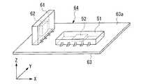
従来では、例えば、図20に示すように、基板63の表面63aに磁気センサ51,61を搭載した磁気センサユニット64が提供されており、この磁気センサユニット64は、外部磁界の方位を3次元的に測定することができる。
【0003】
すなわち、磁気センサ51は、外部磁界の2方向の磁気成分に対して感応する磁気センサチップ52を備えており、その感応方向は、基板63の表面63aに沿って互いに直交する方向(X方向、Y方向)となっている。また、磁気センサ61は、外部磁界の1方向の磁気成分に対して感応する磁気センサチップ62を備えており、その感応方向は、基板63の表面63aに直交する方向(Z方向)となっている。
外部磁界の方位は、これら磁気センサチップ52,62により3次元空間内の3つの磁気成分を検出し、3次元空間内のベクトルとして測定される。
【0004】
【特許文献1】
特開平5−52918号公報
【0005】
【発明が解決しようとする課題】
しかしながら、上記の磁気センサユニット64においては、磁気センサ51,61にそれぞれ1つの磁気センサチップ52,62しか備えていなかったため、各々の磁気センサ51,61を製造して、これらの磁気センサ51,61をそれぞれ基板63の表面63aに搭載する必要があり、結果として、製造工程が多く、製造コストが高くなるという問題があった。
また、磁気センサチップ62の感応方向が磁気センサチップ52の感応方向に直交するように、磁気センサ61を基板63の表面63aに精度よく搭載することが困難であるという問題があった。
【0006】
この発明は、上述した事情に鑑みてなされたものであって、外部磁界の3次元的な方位を正しく測定すると共に、製造コストの削減を図ることができる磁気センサの製造方法を提供することを目的としている。
【0007】
【課題を解決するための手段】
上記課題を解決するために、この発明は以下の手段を提案している。
請求項1に係る発明は、少なくとも2つのステージ部と、その周囲に配されるリードを備えるフレーム部と、これらを連結する連結部とを有する金属製薄板からなるリードフレームであって、前記連結部は、前記ステージ部から突出して前記フレーム部に連結されると共に、塑性変形によって屈曲可能な屈曲部を有することを特徴とするリードフレームを提案している。
この発明に係るリードフレームによれば、フレーム部を固定した状態で、ステージ部を押圧することにより、屈曲部を屈曲させて、ステージ部をフレーム部に対して容易に傾斜させることができる。
【0008】
請求項2に係る発明は、少なくとも2つのステージ部と、その周囲に配されるリードを備えるフレーム部と、これらを連結する連結部と、一方のステージ部から突出して他方のステージ部に連結されるステージ連結部とを有する金属製薄板からなるリードフレームであって、前記ステージ連結部が、塑性変形可能な形状を有することを特徴とするリードフレームを提案している。
この発明に係るリードフレームによれば、フレーム部を固定した状態で、ステージ部を押圧することにより、ステージ連結部を塑性変形させて、2つのステージ部を互いに容易に傾斜させることができる。
【0009】
請求項3に係る発明は、磁界の少なくとも1方向の磁気成分に対して感応する磁気センサチップを備えた磁気センサの製造方法であって、少なくとも2つのステージ部と、その周囲に配されるリードを備えるフレーム部と、これらを連結する連結部とを有する金属製薄板からなるリードフレームを用意する工程と、前記各ステージ部に磁気センサチップを接着する工程と、該磁気センサチップと前記リードとを配線する工程と、前記連結部を塑性変形させ、前記フレーム部に対して前記ステージ部を傾斜させる工程とを備えることを特徴とする磁気センサの製造方法を提案している。
【0010】
請求項4に係る発明は、磁界の少なくとも1方向の磁気成分に対して感応する磁気センサチップを備えた磁気センサの製造方法であって、少なくとも2つのステージ部と、その周囲に配されるリードを備えるフレーム部と、これらを連結する連結部とを有する金属製薄板からなるリードフレームを用意する工程と、前記各ステージ部に磁気センサチップを接着する工程と、該磁気センサチップと前記リードとを配線する工程と、前記連結部および前記ステージ部を塑性変形させ、前記フレーム部に対して前記ステージ部を傾斜させる工程とを備えることを特徴とする磁気センサの製造方法を提案している。
【0011】
請求項5に係る発明は、磁界の少なくとも1方向の磁気成分に対して感応する磁気センサチップを備えた磁気センサの製造方法であって、少なくとも2つのステージ部と、その周囲に配されるリードを備えるフレーム部と、これらを連結する連結部と、一方のステージ部から突出して他方のステージ部に連結されるステージ連結部とを有する金属製薄板からなるリードフレームを用意する工程と、前記各ステージ部に磁気センサチップを接着する工程と、該磁気センサチップと前記リードとを配線する工程と、前記ステージ連結部を塑性変形させ、前記フレーム部に対して前記ステージ部を傾斜させる工程とを備えることを特徴とする磁気センサの製造方法を提案している。
【0012】
この発明に係る磁気センサの製造方法によれば、ステージ部を傾斜させる前に、磁気センサチップを接着するため、各々のステージ部の表面を互いに平行に配して、これらの各表面に磁気センサチップを接着することができ、したがって、複数の磁気センサチップを同時にかつ容易に接着することが可能となる。
そして、ステージ部を傾斜させるように、リードフレームの連結部やステージ部やステージ連結部を塑性変形させるため、複数の磁気センサチップの表面が相互になす角度を容易にかつ精度よく設定することが可能となる。
【0013】
以上のことから、例えば、一の磁気センサチップがその表面に沿って2つの感応方向を有し、他の磁気センサチップがその表面に沿って1つの感応方向を有している場合には、他の磁気センサチップの感応方向を、一の磁気センサチップの2つの感応方向を含む平面に対して精度よく交差させることができる。したがって、これら3つの感応方向により3次元空間内の3つの磁気成分を検出して、磁界の方位を3次元空間内のベクトルとして測定することが可能となり、磁界の方位を正しく測定することができる。
【0014】
【発明の実施の形態】
はじめに、本発明の第1の実施形態に係る磁気センサの製造方法により製造される磁気センサの構成について、図1,2を参照して説明しておく。この磁気センサ1は、外部磁界の向きと大きさを測定するものであり、2つの磁気センサチップ2,3と、これら磁気センサチップ2,3を外部に対して電気的に接続するための複数のリード4と、これら磁気センサチップ2,3およびリード4を一体的に固定する樹脂モールド部5とを備えている。
【0015】
磁気センサチップ2,3は、平面視矩形の板状に形成されており、それぞれステージ部6,7上に搭載されている。また、これら磁気センサチップ2,3は、樹脂モールド部5の内部に埋まっており、各リード4の基端部4aよりも樹脂モールド部5の上面5c側に配置されている。さらに、これら磁気センサチップ2,3は、樹脂モールド部5の下面5aに対して傾斜すると共に、磁気センサチップ2,3の一端部2b,3bが樹脂モールド部5の上面5c側に向くと共に、その表面2a,3aが相互に角度θをもって鋭角に傾斜している。
なお、ここで鋭角とは、ステージ部6の表面6aと、ステージ部7の裏面7bとのなす角度θである。
【0016】
磁気センサチップ2は、外部磁界の2方向の磁気成分に対してそれぞれ感応するものであり、これら2つの感応方向は、磁気センサチップ2の表面2aに沿って互いに直交する方向(A方向およびB方向)となっている。
また、磁気センサチップ3は、外部磁界の1方向の磁気成分に対して感応するものであり、その感応方向は、表面3aに沿ってA,B方向により画定される平面(A−B平面)と鋭角に交差する方向(C方向)となっている。
【0017】
各リード4は、銅材等の金属材料からなり、基端部4a、先端部4b、およびこれら基端部4aおよび先端部4bを連結する連結部4cとから形成され、例えばクランク状の断面形状を有する。
各リード4の基端部4aは、その一部が樹脂モールド部5の内部に埋まっており、金属製のワイヤー8により磁気センサチップ2,3と電気的に接続されている。また、各リード4の先端部4bおよび連結部4cは、樹脂モールド部5の側面5bの外方に位置しており、先端部4bは、樹脂モールド部5の下面5aよりも下方に配置されている。
【0018】
次に、上述した磁気センサ1を製造するための方法を説明する。
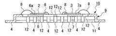
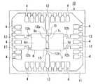
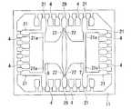
はじめに、薄板状の金属板にプレス加工もしくはエッチング加工、あるいはこの両方の加工を施すことにより、図3,4に示すように、ステージ部6,7がフレーム部9に支持されたリードフレーム10を形成する。
フレーム部9は、ステージ部6,7を囲むように平面視矩形の枠状に形成された矩形枠部11と、この矩形枠部11から内方に向けて突出する複数のリード4,12とからなる。
【0019】
リード(連結部)12は、ステージ部6,7を矩形枠部11に対して固定するための吊りリードであり、その一端部12a,12bが、ステージ部6,7の側端部に固定されている。これらリード12の一端部12a,12bは、ステージ部6,7を傾斜させる際に、容易に塑性変形できる形状となっている。
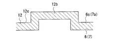
すなわち、一端部12aは、各ステージ部6,7の一端部6c,7c側に固定されており、その両方の側面に凹状の切り欠きを設けて、リード12の他の部分よりも細く形成され、容易に捻ることができる形状となっている。また、一端部(屈曲部)12bは、ステージ部6,7の他端部6d,7d側に固定されており、図5に示すように、リード12の表面12c側に突出するように、予め折り曲げ加工を施し、容易に屈曲することができる形状となっている。
なお、各ステージ部6,7の側端部は、2つのステージ部6,7を並べる方向に直交する各ステージ部6,7の幅方向の端部を示している。また、各ステージ部6,7の一端部6c,7cは、2つのステージ部6,7が相互に対向する端部を示している。さらに、各ステージ部6,7の他端部6d,7dは、2つのステージ部6,7の並列方向に沿って一端部6c,7cの反対側に位置する端部を示している。
【0020】
このリードフレーム10を用意した後に、図3,4に示すように、ステージ部6,7の表面6a,7aにそれぞれ磁気センサチップ2,3を接着すると共に、ワイヤー8を配して磁気センサチップ2,3とリード4とを電気的に接続する。
なお、ワイヤー8を配する際には、ステージ部6,7を傾斜させる段階において、ワイヤー8と磁気センサチップ2,3とのボンディング部分、およびリード4とのボンディング部分が互いに離れるため、ワイヤー8は、その長さもしくは高さに余裕を持たせた状態にて配される。
【0021】
次いで、図6に示すように、ステージ部6,7およびリード12の一端部12a,12bを除いたリードフレーム10の各部を金型D,Eにより挟み込み、この状態において、ステージ部6,7の裏面6b,7b側の他端部6d,7dをピンFにより上方に押圧し、ステージ部6,7と共に磁気センサチップ2,3を相互に所定の角度に傾斜させる。
この際には、各ステージ部6,7の両側に位置する側端部に固定されたリード12の一端部12a,12aを結ぶ軸線(図6の示す破線)回りにステージ部6,7がそれぞれ回転して、一端部12aが捻れるように塑性変形し、一端部12bが屈曲するように塑性変形する。このため、磁気センサチップ2,3は、リード4の基端部4aの形成方向に対して傾斜した状態を保持することになる。
【0022】
そして、磁気センサチップ2,3を搭載したリードフレーム10を別の金型(図示せず)内に配置し、この金型内に溶融樹脂を射出して、磁気センサチップ2,3を樹脂の内部に埋める樹脂モールド部を形成する。これにより、磁気センサチップ2,3が、相互に傾斜した状態にて、樹脂モールド部の内部に固定されることになる。
最後に、矩形枠部11、およびリード12のうち樹脂モールド部の外側に突出する部分を切り落として、図1に示す磁気センサ1の製造が終了する。
【0023】
このように製造された磁気センサ1は、例えば、図示しない携帯端末装置内の基板に搭載され、この携帯端末装置では、磁気センサ1により測定した地磁気の方位を携帯端末装置の表示パネルに示すようになっている。以下に、磁気センサ1による地磁気の方位測定について説明する。
すなわち、磁気センサチップ2,3は、A,B方向およびC方向に沿った地磁気成分をそれぞれ検出し、それぞれの地磁気成分に略比例した値Sa、SbおよびScをそれぞれ出力するようになっている。
【0024】
ここで、地磁気方向がA−B平面に沿っている場合には、出力値Saは、図7に示すように、磁気センサチップ2のB方向が東または西を向いた際にそれぞれ最大値または最小値となり、B方向が南または北を向いている場合に0となる。
また、出力値Sbは、磁気センサチップ2のB方向が北または南を向いている場合にそれぞれ最大値または最小値となり、B方向が東または西を向いている場合に0となる。
なお、グラフ中の出力値SaおよびSbは、実際に磁気センサ1から出力される値を、実際の出力値の最大値と最小値との差の1/2で除した値である。
【0025】
この際に、携帯端末装置の表示パネルに表示する方位は、東を0°として、南、西、および北の順に回転するにつれて角度の値が増大するように定義される方位aを、例えば、下記表1に示した数式に基づいて決定する。
【0026】
【表1】
また、地磁気方向がA−B平面に対して交差している場合には、磁気センサチップ2に加えて、磁気センサチップ3によりC方向に沿った地磁気成分を検出し、この地磁気成分に略比例した値Scを出力する。
なお、出力値Scは、出力値Sa、Sbと同様に、実際に磁気センサ1から出力される値を、実際の出力値の最大値と最小値との差の1/2で除した値となっている。
【0028】
そして、この出力値Scに基づいてA−B平面に直交する方向の磁気成分の値を出力し、この値と出力値Sa、Sbとにより地磁気の方向を3次元空間内のベクトルとして測定する。
なお、A−B平面とC方向とがなす角度θは、0°よりも大きく、90°以下であり、理論上では、0°よりも大きい角度であれば3次元的な地磁気の方位を測定できる。ただし、実際上は20°以上であることが好ましく、30°以上であることがさらに好ましい。
【0029】
上記の磁気センサ1の製造方法によれば、ステージ部6,7を傾斜させる前に、磁気センサチップ2,3を接着するため、各々のステージ部6,7の表面6a,7aを互いに平行に配した状態にて、これらの各表面6a,7aに磁気センサチップ2,3を接着することができる。したがって、これら磁気センサチップ2,3を同時にかつ容易に接着することが可能となり、製造工程を少なくして、磁気センサ1の製造コスト削減を図ることができる。
また、リード12の一端部12bが屈曲部となっているため、ピンFによりステージ部の6,7の他端部6d,7dを押圧する際に、この一端部12bを屈曲させることにより、ステージ部6,7をフレーム部9に対して容易に傾斜させることができる。
【0030】
そして、ステージ部6,7を傾斜させるように、リードフレーム10の一端部12a、12bを塑性変形させるため、これら磁気センサチップ2,3の表面2a,3aが相互になす角度を容易にかつ精度よく設定することが可能となる。
以上のことから、磁気センサチップ3の感応方向を、A−B平面に対して精度よく交差させて、これら3つの感応方向により地磁気の方位を3次元空間内のベクトルとして測定し、3次元空間内における地磁気の方位を正しく測定することができる。
【0031】
次に、図8および図9は、本発明の第2の実施形態を示している。この実施形態においては、図1および図2に示す磁気センサの基本的構成が同一となっており、磁気センサの製造に用いるリードフレームの構成に関して異なっている。ここでは主に、リードフレームの構成、およびこのリードフレームを使用して磁気センサを製造する方法について説明し、図1から図7の構成要素と同一の部分については同一符号を付し、その説明を省略する。
【0032】
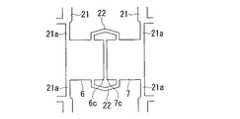
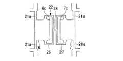
磁気センサを製造する際には、はじめに、薄板状の金属板にプレス加工やエッチング加工を施して、図8に示すように、2つのステージ部6,7がフレーム部19に支持されたリードフレーム20を形成する。このフレーム部19には、矩形枠部11から内方に向けて突出する複数のリード4,21が設けられている。
リード(連結部)21は、ステージ部6,7を矩形枠部11に対して固定するための吊りリードであり、その一端部21aが、ステージ部6,7の他端部6d,7d側の両側に位置する側端部に固定されている。リード21の一端部21aは、リード21の他の部分よりも細く形成されており、容易に捻ることが可能な形状となっている。
また、このリードフレーム20には、一方のステージ部6の一端部6cから突出し、他方のステージ部7の一端部7cに連結されるステージ連結部22が2つ形成されている。このステージ連結部22は、リードフレーム20の厚さ方向に直交する平面上を蛇行する形状となっており、容易に塑性変形できるようになっている。
【0033】
このリードフレーム20を用意した後には、第1の実施形態と同様に、図9に示すように、ステージ部6,7の表面6a,7aにそれぞれ磁気センサチップ2,3を接着すると共に、磁気センサチップ2,3とリード4との間にワイヤー8を配する。
次いで、ステージ部6,7、リード21の一端部21aおよびステージ連結部22を除いたリードフレーム20の各部を金型G,Hにより挟み込み、この状態において、ステージ部6,7の裏面6b,7b側の一端部6c,7cをピンIにより上方に押圧し、ステージ部6,7と共に磁気センサチップ2,3を相互に所定の角度に傾斜させる。
【0034】
この際には、各ステージ部6,7の両側に位置する側端部に固定されたリード21の一端部21a,21aを結ぶ軸線(図9の示す破線)回りにステージ部6,7がそれぞれ回転して、一端部21aが捻れるように塑性変形する。また、この際には、各ステージ部6,7の一端部6c,7cが相互に離間するため、ステージ連結部22が延びるように塑性変形する。このため、磁気センサチップ2,3は、リード4の基端部4aの形成方向に対して傾斜した状態を保持することになる。
最後に、第1の実施形態と同様に、磁気センサチップ2,3を樹脂の内部に埋める樹脂モールド部を形成し、矩形枠部11、およびリード21のうち樹脂モールド部の外側に突出する部分を切り落とすことにより、磁気センサの製造が終了する。
【0035】
上記の磁気センサの製造方法によれば、第1の実施形態と同様に、磁気センサチップ2,3を同時にかつ容易に接着することが可能となり、製造工程を少なくして、磁気センサの製造コスト削減を図ることができる。
また、ステージ連結部22が容易に塑性変形できる形状となっているため、ピンIによりステージ部6,7の一端部6c,7cを押圧する際に、このステージ連結部22を塑性変形させることにより、ステージ部6,7をフレーム部19に対して容易に傾斜させることができる。そして、リード21の一端部21aおよびステージ連結部22を塑性変形させるため、これら磁気センサチップ2,3の表面2a,3aが相互になす角度を容易にかつ精度よく設定することが可能となる。
さらに、このステージ連結部22は、リードフレーム20の厚さ方向に直交する平面上を蛇行する形状となっているため、ステージ連結部22に折り曲げ加工やエッチング加工を施す必要がなく、リードフレーム20の製造を容易に行うことができる。
【0036】
なお、第1の実施形態において、リード12の一端部12bは、リード12の表面12c側に突出した形状であるとしたが、これに限ることはなく、ステージ部6,7を傾斜させる際に、塑性変形が容易な形状であればよい。すなわち、例えば、図10(a)に示すように、リード12の表面12cおよび裏面12dの両方に突出するように折り曲げ加工が施された形状でもよいし、図10(b)に示すように、エッチング加工によりリード12の他の部分の厚さ寸法よりも薄くした形状であってもよい。
また、リード12の一端部12bは、図10(c)に示すように、リードフレーム10の厚さ方向に直交する平面上を蛇行する形状としても良い。この形状の場合には、リード12に折り曲げ加工やエッチング加工を施す必要がないため、リードフレーム10の製造を容易に行うことができる。なお、この形状の場合には、一端部12bをリード12の他の部分よりも細く形成しておくことが好ましい。
【0037】
さらに、リード12の一端部12aを各ステージ部6,7の一端部6c,7c側に位置する側端部に固定するとしたが、これに限ることはなく、少なくともステージ部6,7が、その一端部6c,7c側を中心に回転できるように構成されていればよい。すなわち、例えば、図11に示すように、2つのステージ部6,7の一端部6c,7cをステージ連結部15により連結し、このステージ連結部15にリード12の一端部12aを固定するとしても構わない。
また、リード12の他端部12bを、他端部6d,7d側に位置する各ステージ部6,7の側端部に固定するとしたが、これに限ることはなく、例えば、他端部6d,7dに直接固定するとしても構わない。
【0038】
さらに、磁気センサチップ2,3は、その一端部2b,3bが樹脂モールド部5の上面5c側に向くように傾斜するとしたが、これに限ることはなく、少なくとも磁気センサチップ3の感応方向がA−B平面と交差するように、磁気センサチップ2,3が相互に傾斜すると共に、フレーム部9に対して傾斜していればよい。
ただし、磁気センサチップ2,3の傾斜方向が変わる場合には、この傾斜方向に応じてリードフレーム10の一端部12a,12bの位置を変える必要がある。
【0039】
また、一端部12aは、凹状の切り欠きを有する形状とは限らず、ステージ部6,7を傾斜させる際に容易に塑性変形できる形状であればよい。
さらに、リード12の屈曲部は、ステージ部6,7に隣接する一端部12bに形成されるとしたが、これに限ることはなく、リード12のうち、一端部12bから矩形枠部11に至るまでの間に形成されていればよい。
【0040】
なお、第2の実施形態においては、2つのステージ部6,7を連結するステージ連結部22が2つ形成されるとしたが、これに限ることはなく、例えば、図12に示すように、ステージ連結部22を1つだけ形成するとしても構わない。
また、このステージ連結部22は、リードフレーム20の厚さ方向に直交する平面上を蛇行するように形成されるとしたが、これに限ることはなく、少なくとも容易に塑性変形できるものであればよい。
すなわち、ステージ連結部22は、例えば、図13(a)に示すように、ステージ部6,7を略矩形状の板状体23により連結し、この板状体23に貫通孔23aを形成したものでもよい。また、ステージ連結部22は、例えば、図13(b)に示すように、各ステージ部6,7の一端部6c,7cから突出して漸次先細に形成されたテーパ状の突出部24,25を一対形成し、これら突出部24,25の先端部を相互に連結したものでもよい。
また、例えば、ステージ連結部22の厚みをステージ部6,7の厚さ寸法よりも薄く形成しても構わない。
【0041】
また、ステージ連結部22は、2つのステージ部6,7の一端部6c,7cを相互に連結するとしたが、これに限ることはなく、例えば、図14に示すように、一端部6c,7c側に位置する各ステージ部6,7の側端部を相互に連結するとしても良い。なお、この構成において、ステージ連結部22は幅の細い扇状に形成されており、容易に塑性変形できるようになっている。この構成の場合には、2つのステージ部6,7の一端部6c,7cの隙間にステージ連結部22が存在しないため、この隙間を小さくして2つのステージ部6,7の間隔を小さくすることができる。したがって、このリードフレームを用いることにより磁気センサの小型化を図ることができる。
なお、各ステージ部6,7の側端部に固定されるステージ連結部22は、上述の形状に限ることはなく、例えば、図15に示すように、略矩形の枠状に形成したものであっても良い。また、ステージ連結部22は、例えば、図16や図17に示すように、略矩形の枠状に形成したものと比較して、屈曲する部分をさらに加えたものであっても良い。
【0042】
また、ステージ連結部22は、2つのステージ部6,7を直接連結することだけに限らず、例えば、図18に示すように、一端部6cを囲むようにステージ部6の側端部同士をつなぐ矩形枠部26と、一端部7cを囲むようにステージ部7の側端部同士をつなぐ矩形枠部27と、これら2つの矩形枠部26,27を連結する連結部28とから形成しても構わない。
さらに、ステージ連結部22は、2つのステージ部6,7を相互に連結するだけでなく、例えば、図19に示すように、矩形枠部11から突出するリード29にも連結されるとしても良い。
【0043】
なお、これら第1、第2の実施形態においては、ピンF,Iによりステージ部6,7の他端部6d,7dや一端部6c,7cを押し上げて、磁気センサチップ2,3を傾斜させるとしたが、ピンF,Iによる傾斜に限ることはなく、磁気センサチップ2,3をステージ部6,7の表面6a,7aに接着した後から樹脂モールド部5を形成するまでの間に傾斜させればよい。
また、磁気センサチップ2,3は、ステージ部6,7の表面6a,7aに接着されるとしたが、これに限ることはなく、少なくとも一方の磁気センサチップをステージ部6,7の裏面に接着されるとしてもよい。
【0044】
さらに、磁気センサチップ2,3の2つ使用し、磁気センサチップ3が1つの感応方向を有するとしたが、これに限ることはなく、複数の磁気センサチップを使用し、3つ以上の感応方向が、地磁気の方向を3次元空間内のベクトルとして測定できるように、互いに交差していればよい。
すなわち、例えば、磁気センサチップ3が2つの感応方向を有してもよいし、各々1つの感応方向を有する3つの磁気センサチップを使用するとしてもよい。
【0045】
また、例えば、リードフレーム10の内、ステージ部6,7を含むリード4の基端部4aよりも内側の領域は、ステージ部6,7をさらに容易に傾斜させることができるように、リードフレーム10の他の部分の半分の厚さ寸法としてもよい。
さらに、各リード4は、クランク状の断面形状を有し、その先端部4bが樹脂モールド部5の下面5aよりも下方に配置されるとしたが、これに限ることはなく、リード4の一部が樹脂モールド部5の下面5a側に露出していればよい。
また、リード4、ワイヤー8の数および配置位置は、上記実施形態に限ることはなく、磁気センサチップの種類に応じて、磁気センサチップに対するワイヤー8の接着位置および接着する数を変えると共に、リード4の数および配置位置を変えるとしてよい。
【0046】
さらに、上記実施形態では、リード12,21の一端部12a,12aや一端部21a,21aを結ぶ軸線で回転させるとしたが、これに限ることはなく、これら一端部12a,12aや一端部21a,21aを結ぶ軸線もしくはステージ部のうち、磁気センサチップ2,3が配されていない部分で屈曲させてもよい。
また、磁気センサ1を携帯端末装置に搭載するとしたが、この構成に限定されることはなく、カテーテルやカメラ等の体内に挿入する医療機器に搭載してもよい。例えば、体内に挿入したカメラの方位を測定する場合には、体を貫通する磁界を発生させて、磁気センサ1によりその磁界の方向を測定させる。これにより、磁気センサ1と磁界との相対的な角度を3次元的に測定することができるため、磁界の方向を基準として、カメラの方位を正しく検出することができる。
【0047】
以上、本発明の実施形態について図面を参照して詳述したが、具体的な構成はこの実施形態に限られるものではなく、本発明の要旨を逸脱しない範囲の設計変更等も含まれる。
【0048】
【発明の効果】
以上説明したように、請求項1に係る発明によれば、連結部は、ステージ部から突出してフレーム部に連結されると共に、塑性変形によって屈曲可能な屈曲部を有するため、屈曲部を屈曲させて、ステージ部をフレーム部に対して容易に傾斜させることができる。
また、請求項2に係る発明によれば、ステージ連結部が塑性変形可能であるため、一方のステージ部と他方のステージ部とを相互に容易に傾斜させることができる。
【0049】
また、請求項3から請求項5に係る発明によれば、ステージ部を傾斜させる前に、磁気センサチップを接着するため、複数の磁気センサチップを同時にかつ容易に接着することが可能となり、製造工程を少なくして、磁気センサの製造コスト削減を図ることができる。
【0050】
また、ステージ部を傾斜させるように、リードフレームの連結部やステージ部やステージ連結部を塑性変形させるため、複数の磁気センサチップの表面が相互になす角度を容易にかつ精度よく設定することが可能となる。
したがって、例えば、一の磁気センサチップが2方向の感応方向を、他の磁気センサチップが1方向の感応方向を有している場合には、磁界の方位を3次元空間内のベクトルとして測定し、3次元空間内の磁界の方位を正しく測定できる。
【図面の簡単な説明】
【図1】この発明の第1の実施形態に係る製造方法により製造される磁気センサを示す平面図である。
【図2】図1の磁気センサの側断面図である。
【図3】図1の磁気センサにおいて、リードフレームに磁気センサチップを搭載した状態を示す平面図である。
【図4】図1の磁気センサにおいて、リードフレームに磁気センサチップを搭載した状態を示す側断面図である。
【図5】図3のリードフレームにおいて、リードのN−N矢視断面図である。
【図6】図1の磁気センサにおいて、ステージ部および磁気センサチップを傾斜させる方法を示す側断面図である。
【図7】図1の磁気センサの表面が地磁気の方向に沿って配されている場合における磁気センサの出力値Sa、Sbを示すグラフである。
【図8】この発明の第2の実施形態に係る磁気センサの製造方法に使用するリードフレームを示す平面図である。
【図9】図8のリードフレームを使用して、ステージ部および磁気センサチップを傾斜させる方法を示す側断面図である。
【図10】この発明の他の実施形態に係る製造方法に使用するリードフレームの要部を示す拡大断面図である。
【図11】この発明の他の実施形態に係る磁気センサの製造方法に使用するリードフレームを示す平面図である。
【図12】この発明の他の実施形態に係る磁気センサの製造方法に使用するリードフレームの要部を示す平面図である。
【図13】この発明の他の実施形態に係る磁気センサの製造方法に使用するリードフレームの要部を示す平面図である。
【図14】この発明の他の実施形態に係る磁気センサの製造方法に使用するリードフレームの要部を示す平面図である。
【図15】この発明の他の実施形態に係る磁気センサの製造方法に使用するリードフレームの要部を示す平面図である。
【図16】この発明の他の実施形態に係る磁気センサの製造方法に使用するリードフレームの要部を示す平面図である。
【図17】この発明の他の実施形態に係る磁気センサの製造方法に使用するリードフレームの要部を示す平面図である。
【図18】この発明の他の実施形態に係る磁気センサの製造方法に使用するリードフレームの要部を示す平面図である。
【図19】この発明の他の実施形態に係る磁気センサの製造方法に使用するリードフレームを示す平面図である。
【図20】従来の磁気センサユニットの一例を示す斜視図である。
【符号の説明】
1・・・磁気センサ、2,3・・・磁気センサチップ、4・・・リード、
6,7・・・ステージ部、9,19・・・フレーム部、10,20・・・リードフレーム、12,21・・・リード(連結部)、12b・・・一端部(屈曲部)、22・・・ステージ連結部[0001]
TECHNICAL FIELD OF THE INVENTION
The present invention relates to a method for manufacturing a magnetic sensor for measuring the direction of a magnetic field and a lead frame used for the method.
[0002]
[Prior art]
Generally, a magnetic sensor that detects magnetism is used for measuring the azimuth of an external magnetic field (for example, see Patent Document 1).
Conventionally, for example, as shown in FIG. 20, a
[0003]
That is, the
The direction of the external magnetic field is measured as a vector in the three-dimensional space by detecting three magnetic components in the three-dimensional space by the
[0004]
[Patent Document 1]
JP-A-5-52918 [0005]
[Problems to be solved by the invention]
However, in the
Further, there is a problem that it is difficult to mount the
[0006]
The present invention has been made in view of the above circumstances, and provides a method of manufacturing a magnetic sensor capable of correctly measuring a three-dimensional azimuth of an external magnetic field and reducing manufacturing costs. The purpose is.
[0007]
[Means for Solving the Problems]
In order to solve the above problems, the present invention proposes the following means.
The invention according to
According to the lead frame of the present invention, the bent portion is bent by pressing the stage portion while the frame portion is fixed, so that the stage portion can be easily inclined with respect to the frame portion.
[0008]
According to a second aspect of the present invention, at least two stage portions, a frame portion including leads arranged around the stage portion, a connecting portion for connecting these, and a projecting portion from one stage portion are connected to the other stage portion. A lead frame made of a thin metal plate having a stage connecting portion, wherein the stage connecting portion has a shape capable of being plastically deformed.
According to the lead frame of the present invention, by pressing the stage while the frame is fixed, the stage connecting portion can be plastically deformed, and the two stages can be easily inclined with respect to each other.
[0009]
According to a third aspect of the present invention, there is provided a method of manufacturing a magnetic sensor including a magnetic sensor chip responsive to a magnetic component in at least one direction of a magnetic field, wherein at least two stage portions and leads arranged around the stage portion are provided. A step of preparing a lead frame made of a thin metal plate having a frame part having a connecting part for connecting these, a step of bonding a magnetic sensor chip to each of the stage parts, and the magnetic sensor chip and the lead And a process of plastically deforming the connecting portion and inclining the stage portion with respect to the frame portion.
[0010]
According to a fourth aspect of the present invention, there is provided a method of manufacturing a magnetic sensor including a magnetic sensor chip responsive to a magnetic component in at least one direction of a magnetic field, wherein at least two stage portions and leads arranged around the stage portion are provided. A step of preparing a lead frame made of a thin metal plate having a frame part having a connecting part for connecting these, a step of bonding a magnetic sensor chip to each of the stage parts, and the magnetic sensor chip and the lead And a step of plastically deforming the connecting portion and the stage portion to incline the stage portion with respect to the frame portion, thereby proposing a magnetic sensor manufacturing method.
[0011]
According to a fifth aspect of the present invention, there is provided a method of manufacturing a magnetic sensor including a magnetic sensor chip that is sensitive to a magnetic component in at least one direction of a magnetic field, wherein at least two stages are provided and leads arranged around the stage. A step of preparing a lead frame made of a thin metal plate having a frame portion having a connecting portion connecting these components, and a stage connecting portion projecting from one stage portion and connected to the other stage portion; Bonding a magnetic sensor chip to a stage, wiring the magnetic sensor chip and the lead, and plastically deforming the stage connecting portion, and inclining the stage with respect to the frame. A method for manufacturing a magnetic sensor, comprising:
[0012]
According to the method for manufacturing a magnetic sensor according to the present invention, the surfaces of the respective stage portions are arranged in parallel with each other in order to attach the magnetic sensor chips before the stage portions are inclined, and the magnetic sensor is attached to each of these surfaces. The chips can be bonded, so that a plurality of magnetic sensor chips can be bonded simultaneously and easily.
In order to plastically deform the connecting portion of the lead frame, the stage portion, and the stage connecting portion so as to incline the stage portion, it is possible to easily and accurately set the angle formed by the surfaces of the plurality of magnetic sensor chips with each other. It becomes possible.
[0013]
From the above, for example, if one magnetic sensor chip has two sensitive directions along its surface and the other magnetic sensor chip has one sensitive direction along its surface, The sensitive direction of another magnetic sensor chip can accurately intersect with a plane including two sensitive directions of one magnetic sensor chip. Therefore, it is possible to detect three magnetic components in the three-dimensional space based on these three sensitive directions and measure the direction of the magnetic field as a vector in the three-dimensional space, and to correctly measure the direction of the magnetic field. .
[0014]
BEST MODE FOR CARRYING OUT THE INVENTION
First, the configuration of a magnetic sensor manufactured by the method for manufacturing a magnetic sensor according to the first embodiment of the present invention will be described with reference to FIGS. The
[0015]
The
Here, the acute angle is the angle θ between the
[0016]
The
The
[0017]
Each
A part of the
[0018]
Next, a method for manufacturing the above-described
First, the
The
[0019]
The lead (connecting portion) 12 is a suspension lead for fixing the
That is, the one
In addition, the side end of each
[0020]
After the
When the
[0021]
Next, as shown in FIG. 6, the respective parts of the
At this time, the
[0022]
Then, the
Finally, the portions of the
[0023]
The
That is, the
[0024]
Here, when the terrestrial magnetism direction is along the AB plane, the output value Sa becomes the maximum value or the maximum value when the B direction of the
The output value Sb becomes the maximum value or the minimum value when the B direction of the
The output values Sa and Sb in the graph are values obtained by dividing the value actually output from the
[0025]
At this time, the azimuth to be displayed on the display panel of the mobile terminal device is azimuth a defined such that the value of the angle increases as the east is set to 0 °, and the rotation is performed in the order of south, west, and north, for example, It is determined based on the formula shown in Table 1 below.
[0026]
[Table 1]
If the geomagnetic direction intersects the AB plane, the
The output value Sc is a value obtained by dividing the value actually output from the
[0028]
Then, a value of a magnetic component in a direction orthogonal to the AB plane is output based on the output value Sc, and the direction of the terrestrial magnetism is measured as a vector in a three-dimensional space by using this value and the output values Sa and Sb.
The angle θ formed between the AB plane and the C direction is larger than 0 ° and equal to or smaller than 90 °. In theory, if the angle is larger than 0 °, a three-dimensional azimuth of geomagnetism is measured. it can. However, in practice, it is preferably at least 20 °, more preferably at least 30 °.
[0029]
According to the method of manufacturing the
In addition, since the one
[0030]
Then, since the
From the above, the sensitive direction of the
[0031]
Next, FIGS. 8 and 9 show a second embodiment of the present invention. In this embodiment, the basic configuration of the magnetic sensor shown in FIGS. 1 and 2 is the same, and the configuration of the lead frame used for manufacturing the magnetic sensor is different. Here, the configuration of the lead frame and a method of manufacturing a magnetic sensor using the lead frame will be mainly described, and the same components as those in FIGS. 1 to 7 will be denoted by the same reference numerals. Is omitted.
[0032]
At the time of manufacturing the magnetic sensor, first, a thin metal plate is subjected to press working or etching work to form a lead frame in which two
The lead (connecting portion) 21 is a suspension lead for fixing the
The
[0033]
After preparing the
Next, the respective parts of the
[0034]
At this time, the
Lastly, similarly to the first embodiment, a resin mold portion for filling the
[0035]
According to the method of manufacturing the magnetic sensor described above, similarly to the first embodiment, the
Further, since the
Further, since the
[0036]
In the first embodiment, the one
Further, as shown in FIG. 10C, the one
[0037]
Further, the one
In addition, the
[0038]
Further, the
However, when the inclination direction of the
[0039]
Further, the one
Further, the bent portion of the
[0040]
In the second embodiment, two
The
That is, for example, as shown in FIG. 13A, the
Further, for example, the thickness of the
[0041]
The
The
[0042]
In addition, the
Further, the
[0043]
In the first and second embodiments, the pins F and I push up the
The
[0044]
Furthermore, although two
That is, for example, the
[0045]
Further, for example, in the
Further, each of the
Further, the numbers and the arrangement positions of the
[0046]
Furthermore, in the above-described embodiment, the
Although the
[0047]
As described above, the embodiment of the present invention has been described in detail with reference to the drawings. However, the specific configuration is not limited to this embodiment, and includes a design change or the like without departing from the gist of the present invention.
[0048]
【The invention's effect】
As described above, according to the first aspect of the present invention, since the connecting portion projects from the stage portion and is connected to the frame portion and has a bending portion that can be bent by plastic deformation, the bending portion is bent. Thus, the stage can be easily inclined with respect to the frame.
According to the second aspect of the present invention, since the stage connecting portion can be plastically deformed, the one stage portion and the other stage portion can be easily inclined with respect to each other.
[0049]
According to the inventions according to
[0050]
In addition, since the connecting portion of the lead frame, the stage portion, and the stage connecting portion are plastically deformed so that the stage portion is inclined, the angle formed by the surfaces of the plurality of magnetic sensor chips with each other can be easily and accurately set. It becomes possible.
Therefore, for example, when one magnetic sensor chip has two sensitive directions and the other magnetic sensor chip has one sensitive direction, the magnetic field direction is measured as a vector in a three-dimensional space. And the direction of a magnetic field in a three-dimensional space can be correctly measured.
[Brief description of the drawings]
FIG. 1 is a plan view showing a magnetic sensor manufactured by a manufacturing method according to a first embodiment of the present invention.
FIG. 2 is a side sectional view of the magnetic sensor of FIG. 1;
FIG. 3 is a plan view showing a state where a magnetic sensor chip is mounted on a lead frame in the magnetic sensor of FIG. 1;
FIG. 4 is a side sectional view showing a state where a magnetic sensor chip is mounted on a lead frame in the magnetic sensor of FIG. 1;
FIG. 5 is a cross-sectional view of the lead taken along line NN in the lead frame of FIG. 3;
FIG. 6 is a side sectional view showing a method of inclining a stage section and a magnetic sensor chip in the magnetic sensor of FIG. 1;
FIG. 7 is a graph showing output values Sa and Sb of the magnetic sensor when the surface of the magnetic sensor of FIG. 1 is arranged along the direction of terrestrial magnetism.
FIG. 8 is a plan view showing a lead frame used in a method for manufacturing a magnetic sensor according to a second embodiment of the present invention.
FIG. 9 is a side sectional view showing a method of tilting a stage and a magnetic sensor chip using the lead frame of FIG. 8;
FIG. 10 is an enlarged cross-sectional view showing a main part of a lead frame used in a manufacturing method according to another embodiment of the present invention.
FIG. 11 is a plan view showing a lead frame used in a method of manufacturing a magnetic sensor according to another embodiment of the present invention.
FIG. 12 is a plan view showing a main part of a lead frame used in a method for manufacturing a magnetic sensor according to another embodiment of the present invention.
FIG. 13 is a plan view showing a main part of a lead frame used in a method for manufacturing a magnetic sensor according to another embodiment of the present invention.
FIG. 14 is a plan view showing a main part of a lead frame used in a method for manufacturing a magnetic sensor according to another embodiment of the present invention.
FIG. 15 is a plan view showing a main part of a lead frame used in a method of manufacturing a magnetic sensor according to another embodiment of the present invention.
FIG. 16 is a plan view showing a main part of a lead frame used in a method for manufacturing a magnetic sensor according to another embodiment of the present invention.
FIG. 17 is a plan view showing a main part of a lead frame used in a method of manufacturing a magnetic sensor according to another embodiment of the present invention.
FIG. 18 is a plan view showing a main part of a lead frame used in a method for manufacturing a magnetic sensor according to another embodiment of the present invention.
FIG. 19 is a plan view showing a lead frame used in a method of manufacturing a magnetic sensor according to another embodiment of the present invention.
FIG. 20 is a perspective view showing an example of a conventional magnetic sensor unit.
[Explanation of symbols]
1 ... magnetic sensor, 2,3 ... magnetic sensor chip, 4 ... lead,
6, 7: stage section, 9, 19: frame section, 10, 20: lead frame, 12, 21: lead (connecting section), 12b ... one end section (bending section), 22 ... Stage connection
Claims (5)
Translated fromJapanese前記連結部が、前記ステージ部から突出して前記フレーム部に連結されると共に、塑性変形によって屈曲可能な屈曲部を有することを特徴とするリードフレーム。A lead frame made of a thin metal plate having at least two stage portions, a frame portion provided with leads arranged around the stage portion, and a connecting portion connecting these,
The lead frame, wherein the connecting portion protrudes from the stage portion and is connected to the frame portion, and has a bent portion that can be bent by plastic deformation.
前記ステージ連結部が、塑性変形可能な形状を有することを特徴とするリードフレーム。A metal having at least two stage portions, a frame portion provided with leads arranged around the stage portion, a connecting portion connecting these, and a stage connecting portion projecting from one stage portion and connected to the other stage portion. A lead frame made of a thin plate,
A lead frame, wherein the stage connecting portion has a shape capable of being plastically deformed.
少なくとも2つのステージ部と、その周囲に配されるリードを備えるフレーム部と、これらを連結する連結部とを有する金属製薄板からなるリードフレームを用意する工程と、
前記各ステージ部に磁気センサチップを接着する工程と、
該磁気センサチップと前記リードとを配線する工程と、
前記連結部を塑性変形させ、前記フレーム部に対して前記ステージ部を傾斜させる工程とを備えることを特徴とする磁気センサの製造方法。A method of manufacturing a magnetic sensor comprising a magnetic sensor chip responsive to a magnetic component in at least one direction of a magnetic field,
A step of preparing a lead frame made of a thin metal plate having at least two stage portions, a frame portion having leads arranged around the stage portion, and a connecting portion for connecting these,
Bonding a magnetic sensor chip to each of the stage portions;
Wiring the magnetic sensor chip and the leads;
A step of plastically deforming the connecting portion and inclining the stage portion with respect to the frame portion.
少なくとも2つのステージ部と、その周囲に配されるリードを備えるフレーム部と、これらを連結する連結部とを有する金属製薄板からなるリードフレームを用意する工程と、
前記各ステージ部に磁気センサチップを接着する工程と、
該磁気センサチップと前記リードとを配線する工程と、
前記連結部および前記ステージ部を塑性変形させ、前記フレーム部に対して前記ステージ部を傾斜させる工程とを備えることを特徴とする磁気センサの製造方法。A method of manufacturing a magnetic sensor comprising a magnetic sensor chip responsive to a magnetic component in at least one direction of a magnetic field,
A step of preparing a lead frame made of a thin metal plate having at least two stage portions, a frame portion having leads arranged around the stage portion, and a connecting portion for connecting these,
Bonding a magnetic sensor chip to each of the stage portions;
Wiring the magnetic sensor chip and the leads;
A step of plastically deforming the connecting portion and the stage portion to incline the stage portion with respect to the frame portion.
少なくとも2つのステージ部と、その周囲に配されるリードを備えるフレーム部と、これらを連結する連結部と、一方のステージ部から突出して他方のステージ部に連結されるステージ連結部とを有する金属製薄板からなるリードフレームを用意する工程と、
前記各ステージ部に磁気センサチップを接着する工程と、
該磁気センサチップと前記リードとを配線する工程と、
前記ステージ連結部を塑性変形させ、前記フレーム部に対して前記ステージ部を傾斜させる工程とを備えることを特徴とする磁気センサの製造方法。A method of manufacturing a magnetic sensor comprising a magnetic sensor chip responsive to a magnetic component in at least one direction of a magnetic field,
A metal having at least two stage portions, a frame portion provided with leads arranged around the stage portion, a connecting portion connecting these, and a stage connecting portion projecting from one stage portion and connected to the other stage portion. A step of preparing a lead frame made of a thin plate;
Bonding a magnetic sensor chip to each of the stage portions;
Wiring the magnetic sensor chip and the leads;
A step of plastically deforming the stage connection portion and inclining the stage portion with respect to the frame portion.
Priority Applications (11)
| Application Number | Priority Date | Filing Date | Title |
|---|---|---|---|
| JP2003202105AJP3823955B2 (en) | 2002-07-29 | 2003-07-25 | Magnetic sensor manufacturing method and lead frame |
| KR20030052057AKR100563584B1 (en) | 2002-07-29 | 2003-07-28 | Manufacturing method for magnetic sensor and lead frame therefor |
| US10/627,717US7187063B2 (en) | 2002-07-29 | 2003-07-28 | Manufacturing method for magnetic sensor and lead frame therefor |
| TW92120514ATWI255346B (en) | 2002-07-29 | 2003-07-28 | Manufacturing method for magnetic sensor and lead frame therefor |
| CNB031555071ACN100346168C (en) | 2002-07-29 | 2003-07-28 | Manufacturing method of magnetic sensor and lead frame thereof |
| EP20030017083EP1387146A3 (en) | 2002-07-29 | 2003-07-28 | Manufacturing method for magnetic sensor and lead frame therefor |
| EP20070022605EP1892537B1 (en) | 2002-07-29 | 2003-07-28 | Three-axis magnetic sensor |
| US11/214,986US8138757B2 (en) | 2002-07-29 | 2005-08-31 | Manufacturing method for magnetic sensor and lead frame therefor |
| KR1020050090629AKR100562096B1 (en) | 2002-07-29 | 2005-09-28 | Manufacturing method for magnetic sensor and lead frame therefor |
| US11/418,251US7541665B2 (en) | 2002-07-29 | 2006-05-05 | Lead frame for a magnetic sensor |
| US11/593,588US7494838B2 (en) | 2002-07-29 | 2006-11-07 | Manufacturing method for magnetic sensor and lead frame therefor |
Applications Claiming Priority (2)
| Application Number | Priority Date | Filing Date | Title |
|---|---|---|---|
| JP2002220413 | 2002-07-29 | ||
| JP2003202105AJP3823955B2 (en) | 2002-07-29 | 2003-07-25 | Magnetic sensor manufacturing method and lead frame |
Publications (2)
| Publication Number | Publication Date |
|---|---|
| JP2004128474Atrue JP2004128474A (en) | 2004-04-22 |
| JP3823955B2 JP3823955B2 (en) | 2006-09-20 |
Family
ID=32300622
Family Applications (1)
| Application Number | Title | Priority Date | Filing Date |
|---|---|---|---|
| JP2003202105AExpired - Fee RelatedJP3823955B2 (en) | 2002-07-29 | 2003-07-25 | Magnetic sensor manufacturing method and lead frame |
Country Status (1)
| Country | Link |
|---|---|
| JP (1) | JP3823955B2 (en) |
Cited By (4)
| Publication number | Priority date | Publication date | Assignee | Title |
|---|---|---|---|---|
| WO2006040987A1 (en)* | 2004-10-08 | 2006-04-20 | Yamaha Corporation | Method of producing physical quantity sensor |
| WO2008123232A1 (en)* | 2007-03-30 | 2008-10-16 | Rohm Co., Ltd. | Semiconductor light emitting device |
| US7642773B2 (en) | 2006-02-23 | 2010-01-05 | Nec Corporation | Magnetic sensor, production method thereof, rotation detection device, and position detection device |
| EP2752675A4 (en)* | 2011-08-30 | 2015-11-25 | Multidimension Technology Co Ltd | Mtj three-axis magnetic field sensor and encapsulation method thereof |
- 2003
- 2003-07-25JPJP2003202105Apatent/JP3823955B2/ennot_activeExpired - Fee Related
Cited By (7)
| Publication number | Priority date | Publication date | Assignee | Title |
|---|---|---|---|---|
| WO2006040987A1 (en)* | 2004-10-08 | 2006-04-20 | Yamaha Corporation | Method of producing physical quantity sensor |
| US7754130B2 (en) | 2004-10-08 | 2010-07-13 | Yamaha Corporation | Method for manufacturing physical quantity sensor |
| US7642773B2 (en) | 2006-02-23 | 2010-01-05 | Nec Corporation | Magnetic sensor, production method thereof, rotation detection device, and position detection device |
| WO2008123232A1 (en)* | 2007-03-30 | 2008-10-16 | Rohm Co., Ltd. | Semiconductor light emitting device |
| JP2008251938A (en)* | 2007-03-30 | 2008-10-16 | Rohm Co Ltd | Semiconductor light emitting device |
| US8334548B2 (en) | 2007-03-30 | 2012-12-18 | Rohm Co., Ltd. | Semiconductor light emitting device |
| EP2752675A4 (en)* | 2011-08-30 | 2015-11-25 | Multidimension Technology Co Ltd | Mtj three-axis magnetic field sensor and encapsulation method thereof |
Also Published As
| Publication number | Publication date |
|---|---|
| JP3823955B2 (en) | 2006-09-20 |
Similar Documents
| Publication | Publication Date | Title |
|---|---|---|
| US7867827B2 (en) | Physical quantity sensor, lead frame, and manufacturing method therefor | |
| KR100563584B1 (en) | Manufacturing method for magnetic sensor and lead frame therefor | |
| JP4214853B2 (en) | Magnetic sensor | |
| JP3823954B2 (en) | Magnetic sensor manufacturing method and lead frame | |
| JP2004128474A (en) | Method of manufacturing magnetic sensor and lead frame | |
| JP3823953B2 (en) | Magnetic sensor manufacturing method and lead frame | |
| JP3823956B2 (en) | Magnetic sensor manufacturing method and lead frame | |
| JP2004191065A (en) | Magnetometric sensor and its manufacturing method | |
| JP4487696B2 (en) | Physical quantity sensor and method of manufacturing physical quantity sensor | |
| CN100514620C (en) | Manufacturing method for magnetic sensor and lead frame therefor | |
| JP4241672B2 (en) | Method for manufacturing physical quantity sensor and lead frame | |
| JP4151667B2 (en) | Manufacturing method of physical quantity sensor and bonding apparatus | |
| JP2006108359A (en) | Lead frame and physical quantity sensor | |
| JP4314580B2 (en) | Physical quantity sensor and lead frame used therefor | |
| JP4622507B2 (en) | Method for manufacturing physical quantity sensor and lead frame | |
| JP2007147649A (en) | Magnetic sensor and magnetic sensor unit | |
| JPH0523140U (en) | Acceleration sensor | |
| JP2006134922A (en) | Lead frame and physical value sensor using this, and further, method of packaging physical value sensor chip | |
| JPH102944A (en) | Magnetic sensor | |
| JP2006269859A (en) | Physical quantity sensor and lead frame used therefor | |
| JP2006120925A (en) | Lead frame and physical quantity sensor | |
| JP2006135279A (en) | Physical quantity sensor and method of manufacturing physical quantity sensor | |
| JP2006108561A (en) | Manufacturing process of physical value sensor |
Legal Events
| Date | Code | Title | Description |
|---|---|---|---|
| A621 | Written request for application examination | Free format text:JAPANESE INTERMEDIATE CODE: A621 Effective date:20040705 | |
| A977 | Report on retrieval | Free format text:JAPANESE INTERMEDIATE CODE: A971007 Effective date:20050105 | |
| A131 | Notification of reasons for refusal | Free format text:JAPANESE INTERMEDIATE CODE: A131 Effective date:20060221 | |
| A521 | Request for written amendment filed | Free format text:JAPANESE INTERMEDIATE CODE: A523 Effective date:20060424 | |
| TRDD | Decision of grant or rejection written | ||
| A01 | Written decision to grant a patent or to grant a registration (utility model) | Free format text:JAPANESE INTERMEDIATE CODE: A01 Effective date:20060606 | |
| A61 | First payment of annual fees (during grant procedure) | Free format text:JAPANESE INTERMEDIATE CODE: A61 Effective date:20060619 | |
| R150 | Certificate of patent or registration of utility model | Free format text:JAPANESE INTERMEDIATE CODE: R150 | |
| S531 | Written request for registration of change of domicile | Free format text:JAPANESE INTERMEDIATE CODE: R313532 | |
| R350 | Written notification of registration of transfer | Free format text:JAPANESE INTERMEDIATE CODE: R350 | |
| FPAY | Renewal fee payment (event date is renewal date of database) | Free format text:PAYMENT UNTIL: 20090707 Year of fee payment:3 | |
| FPAY | Renewal fee payment (event date is renewal date of database) | Free format text:PAYMENT UNTIL: 20100707 Year of fee payment:4 | |
| FPAY | Renewal fee payment (event date is renewal date of database) | Free format text:PAYMENT UNTIL: 20100707 Year of fee payment:4 | |
| FPAY | Renewal fee payment (event date is renewal date of database) | Free format text:PAYMENT UNTIL: 20110707 Year of fee payment:5 | |
| FPAY | Renewal fee payment (event date is renewal date of database) | Free format text:PAYMENT UNTIL: 20110707 Year of fee payment:5 | |
| FPAY | Renewal fee payment (event date is renewal date of database) | Free format text:PAYMENT UNTIL: 20120707 Year of fee payment:6 | |
| FPAY | Renewal fee payment (event date is renewal date of database) | Free format text:PAYMENT UNTIL: 20130707 Year of fee payment:7 | |
| LAPS | Cancellation because of no payment of annual fees |