JP2004111761A - Vapor phase growth method - Google Patents
Vapor phase growth methodDownload PDFInfo
- Publication number
- JP2004111761A JP2004111761AJP2002274228AJP2002274228AJP2004111761AJP 2004111761 AJP2004111761 AJP 2004111761AJP 2002274228 AJP2002274228 AJP 2002274228AJP 2002274228 AJP2002274228 AJP 2002274228AJP 2004111761 AJP2004111761 AJP 2004111761A
- Authority
- JP
- Japan
- Prior art keywords
- raw material
- cvd
- cvd raw
- vapor phase
- phase growth
- Prior art date
- Legal status (The legal status is an assumption and is not a legal conclusion. Google has not performed a legal analysis and makes no representation as to the accuracy of the status listed.)
- Pending
Links
Images


Landscapes
- Formation Of Insulating Films (AREA)
- Chemical Vapour Deposition (AREA)
Abstract
Translated fromJapaneseDescription
Translated fromJapanese【0001】
【発明の属する技術分野】
本発明は、半導体製造装置にガス状のCVD原料を供給し強誘電体膜を成膜する気相成長方法に関する。さらに詳細には、固体CVD原料を有機溶媒に溶解させた原料の混合気化ガスを、FTIRを用いて組成を監視しながら半導体製造装置へ供給し、PZT、BST、SBT、PLZT等の強誘電体膜を成膜する気相成長方法に関する。
【0002】
【従来の技術】
近年、半導体分野においては、半導体メモリー用の酸化物系誘電体膜として、高誘電率を有しステップカバレッジ性が高いチタン酸ジルコン酸鉛(PZT)膜、チタン酸ストロンチウムバリウム(BST)膜、タンタル酸ビスマスストロンチウム(SBT)膜、チタン酸ジルコン酸ランタン鉛(PLZT)膜等が用いられている。これらの半導体膜のCVD原料としては、例えばPb源としてPb(DPM)2(固体原料)、Zr源としてZr(OC(CH3)3)4(液体原料)、Zr(DPM)4(固体原料)、Ti源としてTi(OCH(CH3)2)4(液体原料)、Ti(OCH(CH3)2)2(DPM)2(固体原料)、Ba源としてBa(DPM)2(固体原料)、Sr源としてSr(DPM)2(固体原料)が用いられている。
【0003】
CVD原料として液体原料を使用する場合、通常は、液体原料がキャリアガスとともに気化器に供給され、気化器でガス状にされた後、CVD装置に供給される。しかし、液体原料は、一般的に蒸気圧が低く、粘度が高く、気化温度と分解温度が接近しているため、その品質を低下させることなく、しかも所望の濃度及び流量で効率よく気化させることは困難なことであった。また、固体原料は、高温に保持し昇華して気化供給することにより高純度の原料を得ることが可能であるが、工業的には充分な供給量を確保することが極めて困難であるため、通常はテトラヒドロフラン等の溶媒に溶解させて液体原料とすることにより気化させて使用している。しかし、固体原料は、気化温度が溶媒と大きく相異し、加熱により溶媒のみが気化して固体原料が析出しやすいので、液体原料の気化よりもさらに困難であった。
【0004】
このように液体原料または固体原料を用いた半導体膜の製造は、高度の技術を必要とするが、高品質、高純度のものが期待できるため、これらの原料を劣化や析出をさせることなく効率よく気化する目的で、種々の気化器が開発されてきた。
このような気化器としては、例えば、気化室の形状が、球形、楕球形、樽形、円筒形等であり、キャリヤーガスが気化室内で旋回流を形成するような向きに設定され、気化室の中央部には形状が気化室の形状に略相似形で加熱手段が付与された突起が設けられている気化器が挙げられる(特開2000−315686)。
【0005】
【発明が解決しようとする課題】
前記気化器によれば、加熱されたキャリヤーガスが、気化室の内壁面と突起の間隙を滑らかに旋回し、このような加熱されたキャリヤーガスの流れにより、気化室の内壁及び気化室の中央部の突起からの熱伝達が容易になり、気化室内の温度の均一化をはかることができるので、複数種類のCVD原料の気化においても、各CVD原料の品質の低下を抑制することが可能であり効率よく気化させることができるとされている。
【0006】
しかしながら、このような気化効率が優れた気化器を用いても、PZT膜、BST膜、SBT膜、あるいはPLZT膜の気相成長を行なう際に、固体CVD原料を有機溶媒に溶解させた原料を用いた場合は、気化器内の原料流路には長時間の使用により固体CVD原料が析出して原料の流路内に付着し、絶縁薄膜の品質、純度に悪影響を及ぼす虞があった。このような固体CVD原料の付着に関しては、気化器内の原料流路に圧力計を設置して圧力を監視することにより原料流路の閉塞を予知することができ、圧力が上昇し始める際に気化供給及び気相成長を中断して洗浄することにより気化器内を浄化することができるが、相当量の固体CVD原料が付着しないと、固体CVD原料の付着自体は検知することができなかった。そのため、品質、純度が優れた強誘電体膜を確実に得るためには、洗浄サイクルを短くする必要があり、歩留りが低下するという不都合があった。
【0007】
従って、本発明が解決しようとする課題は、これらの強誘電体膜の気相成長において、気化器内の原料流路における固体CVD原料の付着を容易に検知することができ、歩留りを低下させることなく、品質、純度が優れた強誘電体膜が得られる気相成長方法を提供することである。
【0008】
【課題を解決するための手段】
本発明者らは、これらの課題を解決すべく鋭意検討した結果、CVD原料の混合気化ガスを、FTIRを用いてその成分を分析、監視しながら半導体製造装置へ供給することにより、気化器内の原料流路における固体CVD原料の付着を検知することが可能となり、効率の良い洗浄サイクルで気化器を浄化することにより、歩留りを低下させることなく、品質、純度が優れた強誘電体膜が得られることを見い出し本発明に到達した。
【0009】
すなわち本発明は、鉛を含むCVD原料、ジルコニウムを含むCVD原料、及びチタンを含むCVD原料の混合気化ガスを、FTIRを用いて該混合気化ガスの成分を分析しながら半導体製造装置へ供給し、PZT膜を成膜することを特徴とする気相成長方法である。
【0010】
また、本発明は、バリウムを含むCVD原料、ストロンチウムを含むCVD原料、及びチタンを含むCVD原料の混合気化ガスを、FTIRを用いて該混合気化ガスの成分を分析しながら半導体製造装置へ供給し、BST膜を成膜することを特徴とする気相成長方法である。
【0011】
また、本発明は、ストロンチウムを含むCVD原料、ビスマスを含むCVD原料、及びタンタルを含むCVD原料の混合気化ガスを、FTIRを用いて該混合気化ガスの成分を分析しながら半導体製造装置へ供給し、SBT膜を成膜することを特徴とする気相成長方法である。
【0012】
また、本発明は、鉛を含むCVD原料、ランタンを含むCVD原料、ジルコニウムを含むCVD原料、及びチタンを含むCVD原料の混合気化ガスを、FTIRを用いて該混合気化ガスの成分を分析しながら半導体製造装置へ供給し、PLZT膜を成膜することを特徴とする気相成長方法でもある。
【0013】
【発明の実施の形態】
本発明は、PZT膜、BST膜、SBT膜、またはPLZT膜の気相成長方法に適用される。
本発明の気相成長方法は、PZT膜、BST膜、SBT膜、またはPLZT膜の気相成長方法であって、これらの成膜に用いられるCVD原料の混合気化ガスを、FTIRを用いてその成分を分析しながら半導体製造装置へ供給し、気相成長する方法である。
【0014】
本発明の気相成長方法に適用できるPZT膜、BST膜、SBT膜、またはPLZT膜の成膜に用いられるCVD原料は、常温、常圧で液体であっても、また固体を溶媒に溶解したものであっても、液状を保持し得るものであれば特に制限はなく、用途に応じて適宜選択、使用される。例えば鉛を含むCVD原料としては、ビス(2,2,6,6,−テトラメチル−3,5ヘプタンジオナイト)鉛(Pb(DPM)2)等、ジルコニウムを含むCVD原料としては、テトラtert−ブトキシジルコニウム(Zr(OC(CH3)3)4)、テトラn−ブトキシジルコニウム(Zr(OC4H9)4)、テトラジメチルアミノジルコニウム(Zr(N(CH3)2)4)、テトラ(2,2,6,6,−テトラメチル−3,5ヘプタンジオナイト)ジルコニウム(Zr(DPM)4)、(イソプロポキシ)トリス(2,2,6,6,−テトラメチル−3,5,−ヘプタンジオナイト)ジルコニウム(Zr(OiPr)(DPM)3)、テトラ(2,6,−ジメチル−3,5ヘプタンジオナイト)ジルコニウム(Zr(DMHD)4)等を挙げることができる。
【0015】
また、チタンを含むCVD原料としては、テトラiso−プロポキシチタン(Ti(OCH(CH3)2)4)、テトラn−プロポキシチタン(Ti(OC3H7)4)、テトラジメチルアミノチタン(Ti(N(CH3)2)4)、テトラジエチルアミノチタン(Ti(N(C2H5)2)4)、テトラ(2,2,6,6,−テトラメチル−3,5ヘプタンジオナイト)チタン(Ti(DPM)4)、(ジ−ターシャリーブトキシ)ビス(2,2,6,6,−テトラメチル−3.5.ヘプタンジオナイト)チタン(Ti(OtBu)2(DPM)2)、(ジ−イソプロポキシ)ビス(2,2,6,6,−テトラメチル−3,5,−ヘプタンジオナイト)チタン(Ti(OiPr)2(DPM)2)等を例示することができる。
【0016】
また、バリウムを含むCVD原料としては、ビス(2,2,6,6,−テトラメチル−3,5ヘプタンジオナイト)バリウム(Ba(DPM)2)等、ストロンチウムを含むCVD原料としては、ビス(2,2,6,6,−テトラメチル−3,5ヘプタンジオナイト)ストロンチウム(Sr(DPM)2)等、ビスマスを含むCVD原料としては、ビスマス(III)ターシャリーブトキシド(Bi(OtBu)3)、ビスマス(III)ターシャリーペントキシド(Bi(OtAm)3)、トリフェニルビスマス(BiPh3)等を例示することができる。
【0017】
また、タンタルを含むCVD原料としては、ペンタエトキシタンタル(Ta(OC2H5)5)、ペンタジメチルアミノタンタル(Ta(N(CH3)2)5)、ペンタジエチルアミノタンタル(Ta(N(C2H5)2)5)、(ジ−イソプロポキシ)トリス(2,2,6,6,−テトラメチル−3,5,−ヘプタンジオナイト)タンタル(Ta(OiPr)2(DPM)3)等、ランタンを含むCVD原料としては、トリス(2,2,6,6,−テトラメチル−3,5ヘプタンジオナイト)ランタン(La(DPM)3)等を例示することができる。
ただし、これらのうち固体のCVD原料は、通常は0.1〜1.0mol/L程度の濃度で有機溶媒に溶解して使用する必要がある。
【0018】
固体CVD原料の溶媒として用いられる前記有機溶媒は、通常はその沸点温度が40℃〜140℃の有機溶媒である。それらの有機溶媒として、例えば、プロピルエーテル、メチルブチルエーテル、エチルプロピルエーテル、エチルブチルエーテル、酸化トリメチレン、テトラヒドロフラン、テトラヒドロピラン等のエーテル、メチルアルコール、エチルアルコール、プロピルアルコール、ブチルアルコール等のアルコール、アセトン、エチルメチルケトン、iso−プロピルメチルケトン、iso−ブチルメチルケトン等のケトン、プロピルアミン、ブチルアミン、ジエチルアミン、ジプロピルアミン、トリエチルアミン等のアミン、酢酸エチル、酢酸プロピル、酢酸ブチル等のエステル、ヘキサン、ヘプタン、オクタン等の炭化水素等を挙げることができる。
【0019】
以下、本発明の気相成長方法を、図1に基づいて詳細に説明するが、本発明はこれらにより限定されるものではない。
図1は、本発明の気相成長方法を実施するためのCVD原料の気化供給装置及び半導体製造装置の例を示す構成図である。
【0020】
本発明の気相成長方法に使用される気化供給装置は、例えば、図1のように、CVD原料2が封入されたCVD原料容器3、脱ガス器4、液体マスフローコントローラー等の液体流量制御部5、気化器6、キャリアガス供給ライン9等からなる気化ラインを含むものである。気化ラインは、PZT膜、BST膜、またはSBT膜を気相成長する際には通常3ライン、PLZT膜を気相成長する際には通常4ライン設定される。本発明の気相成長方法においては、各々の気化ラインから供給されたCVD原料の気化ガスを気化ガス混合器10で混合した後、その混合気化ガスの成分を分析するためのFTIR11が設けられる。
【0021】
本発明の気相成長方法においては、例えば、CVD原料が封入されたCVD原料容器を各気化供給ラインに設置した後、CVD原料容器内に不活性ガスの圧力をかけることにより、液体CVD原料が脱ガス器を経由して液体マスフローコントローラーに導入され、さらに気化器へ供給されて気化される。気化器は、液体CVD原料を気化するための気化室、液体CVD原料を気化室へ噴霧するための噴霧ノズル、気化ガス排出口、気化室を加熱するためのヒーター等により構成されるが、特に固体CVD原料を有機溶媒に溶解させた原料を用いた場合は、長時間の気化供給により、噴霧ノズル、気化室のCVD原料噴出口近辺には、固体CVD原料が析出、付着し、CVD原料の気化ガス供給量の低下、変質成分の発生等により、絶縁薄膜の品質、純度に悪影響を及ぼす虞があった。
【0022】
本発明の気相成長方法においては、図1に示すように、各々の気化ラインから供給されたCVD原料の気化ガスを混合した後、その混合気化ガスの成分をFTIRで測定するので、前述のような固体CVD原料の析出、付着、閉塞によるCVD原料の成分変化、変質成分の発生を容易に検知することができる。また、本発明においては、固体CVD原料の析出、付着、閉塞のほか、気化供給装置のトラブルによるCVD原料成分の組成変化等も検知することが可能である。
【0023】
本発明の気相成長方法は、以上のように気化器における固体CVD原料の析出、付着、あるいは閉塞を容易に検知することができるので、これによる各CVD原料の増減を検知し、例えばシーケンサーを設けて電気信号により液体流量制御部のCVD原料の流量を制御することができる。また、本発明は、効率の良い洗浄サイクルで気化器を浄化することが可能であり、歩留りを低下させることなく、品質、純度が優れたPZT、BST、SBT、PLZT等の強誘電体膜が得られる。
【0024】
【実施例】
次に、本発明を実施例により具体的に説明するが、本発明がこれらにより限定されるものではない。
【0025】
実施例1
(気化器の製作)
噴霧ノズル部に超音波振動子を有する図2に示すような気化器を3個製作した。気化室は内径110mmの球形であり、CVD原料供給口が気化室の最上部に、気化ガス出口が気化室の下部に、キャリアガス導入口が気化容器の上部に設けられている。キャリアガス導入管の向きは、キャリアガスが気化室内壁水平面の接線方向に供給され、気化室内で旋回流を形成するような向きに設定されている。また、CVD原料の導入部には、気化器内のCVD原料詰りによる圧力上昇を検知するための圧力計を設けた。尚、この気化器は、液体CVD原料が超音波振動子により霧化され、さらに気化室内の加熱されたキャリアガスの旋回流と接触する構成なので、液体CVD原料を効率よく容易に気化することが可能である。
【0026】
(気化供給装置の製作)
次に、Pb(DPM)2をTHFに溶解した原料が封入された原料容器、Zr(DPM)4をTHFに溶解した原料が封入された原料容器、Ti(OiPr)2(DPM)2をTHFに溶解した原料が封入された原料容器(固体CVD原料の濃度はいずれも0.3mol/L)を、各々脱ガス器、液体マスフローコントローラー、気化器、キャリアガス供給ライン等に接続し、気化ラインを3個製作した。さらに、これらの気化ラインと、気化ガス混合器、FTIRを接続して、気化供給装置を製作するとともに、気化供給装置と半導体製造装置を接続して図1に示すような構成の装置を製作した。
【0027】
(気相成長試験)
半導体製造装置にシリコン基板をセットし、温度を700℃とするとともに、気化器内を1.6kPa(12torr)、230℃、気化ガス混合器の混合室を230℃に保持した。次にPb(DPM)2/THF、Zr(DPM)4/THF、及びTi(OiPr)2(DPM)2/THFを、液体マスフローコントローラーを用いて、各々0.36g/min、0.2g/min、0.2g/minの流量で各々の気化器に供給するとともに、各々のキャリアガス供給ラインから230℃に加熱されたアルゴンガスを、200ml/minの流量で気化器に供給して気化させた。さらに気化ガス混合器から排出される混合気化ガスに、230℃に加熱された高純度の酸素を500ml/minの流量で添加して半導体製造装置に供給してシリコン基板上にPZT膜を成膜した。
【0028】
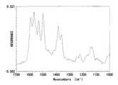
この間、FTIRを用いて10分間隔で混合気化ガスの成分を分析した。その結果、気相成長試験開始直後は、図3に示すような赤外線吸収スペクトルが得られたが、気相成長試験開始から2.5時間後には、図4に示すように気相成長試験開始直後のデータとは若干異なる赤外線吸収スペクトルが得られため、気相成長を一時中断し、気化器をTHFで洗浄してから再度気相成長を行なった。尚、このような状況の変化は、圧力計では検知することができなかった。その後、前記のような操作を繰返して行ない気相成長試験を終了した。この間に得られたPZT膜の蛍光X線分析による組成比率測定の経時変化を表1に示す。表1に示す試験経過時間は、洗浄に要した時間(約10分)を省いた時間である。
【0029】
比較例1
実施例1においてFTIRを使用しなかった以外は実施例1と同様にして気相成長試験を行なった。その結果、気相成長試験開始から10時間後に、CVD原料の導入部の圧力上昇を検知したため気相成長を中止した。この間に得られたPZT膜の蛍光X線分析による組成測定の経時変化を表1に示す。
【0030】
【表1】
【発明の効果】
本発明の気相成長方法は、CVD原料の混合気化ガスの成分を、FTIRを用いて分析、監視しながら気相成長を行なうので、気化器内の原料流路における固体CVD原料の付着や気化供給装置のトラブルによるCVD原料成分の組成変化等を、迅速かつ容易に検知することが可能である。その結果、効率の良い洗浄サイクルで気化器等を浄化することが可能となり、歩留りを低下させることなく、品質、純度が優れたPZT膜、BST膜、SBT膜、PLZT膜等の強誘電体膜が得られようになった。
【図面の簡単な説明】
【図1】本発明の気相成長方法を実施するためのCVD原料の気化供給装置及び半導体製造装置の一例を示す構成図
【図2】本発明の気相成長方法を実施するための気化器の一例を示す断面図
【図3】実施例1における気相成長試験開始直後の混合気化ガスの赤外線吸収スペクトル
【図4】実施例1における気相成長試験開始から2.5時間後の混合気化ガスの赤外線吸収スペクトル
【符号の説明】
1 不活性ガス供給ライン
2 CVD原料
3 CVD原料容器
4 脱ガス器
5 液体マスフローコントローラー
6 気化器
7 ガス予熱器
8 気体マスフローコントローラー
9 キャリアガス供給ライン
10 気化ガス混合器
11 FTIR
12 断熱材
13 半導体製造装置
14 超音波振動子
15 CVD原料噴出口
16 キャリアガス供給管
17 気化ガス排出管
18 気化室
19 ヒーター[0001]
TECHNICAL FIELD OF THE INVENTION
The present invention relates to a vapor phase growth method for forming a ferroelectric film by supplying a gaseous CVD material to a semiconductor manufacturing apparatus. More specifically, a mixed vaporized gas of a raw material obtained by dissolving a solid CVD raw material in an organic solvent is supplied to a semiconductor manufacturing apparatus while monitoring the composition using FTIR, and a ferroelectric material such as PZT, BST, SBT, or PLZT is supplied. The present invention relates to a vapor deposition method for forming a film.
[0002]
[Prior art]
In recent years, in the field of semiconductors, lead oxide zirconate titanate (PZT) film, strontium barium titanate (BST) film, tantalum film, which has a high dielectric constant and high step coverage, has been used as an oxide dielectric film for semiconductor memory. A bismuth strontium titanate (SBT) film, a lead lanthanum zirconate titanate (PLZT) film, or the like is used. As a CVD raw material for these semiconductor films, for example, Pb (DPM)2 (solid raw material) as a Pb source, Zr (OC (CH3 )3 )4 (liquid raw material), Zr (DPM)4 (solid raw material) as a Zr source ), Ti (OCH (CH3 )2 )4 (liquid raw material), Ti (OCH (CH3 )2 )2 (DPM)2 (solid raw material) as a Ti source, and Ba (DPM)2 (solid raw material) as a Ba source ), Sr (DPM)2 (solid raw material) is used as the Sr source.
[0003]
When a liquid raw material is used as a CVD raw material, usually, the liquid raw material is supplied to a vaporizer together with a carrier gas, gasified by the vaporizer, and then supplied to a CVD apparatus. However, liquid raw materials generally have a low vapor pressure, a high viscosity, and a vaporization temperature and decomposition temperature are close to each other. Therefore, the liquid raw material must be efficiently vaporized at a desired concentration and flow rate without lowering its quality. Was difficult. In addition, a solid raw material can be obtained at a high temperature by sublimation and sublimation to provide a high-purity raw material, but it is extremely difficult to secure a sufficient supply industrially, Usually, it is used after being dissolved in a solvent such as tetrahydrofuran to be vaporized by forming a liquid raw material. However, the solid raw material has a significantly different vaporization temperature from that of the solvent, and is more difficult to vaporize than the liquid raw material, because only the solvent is vaporized by heating and the solid raw material is easily precipitated.
[0004]
As described above, the production of a semiconductor film using a liquid raw material or a solid raw material requires advanced technology, but since high quality and high purity can be expected, these materials can be efficiently manufactured without deteriorating or depositing these materials. Various vaporizers have been developed for better vaporization.
As such a vaporizer, for example, the shape of the vaporization chamber is spherical, oval, barrel, cylindrical, or the like, and the carrier gas is set in such a direction as to form a swirling flow in the vaporization chamber. Is provided with a projection provided with a heating means in a central portion substantially similar to the shape of the vaporization chamber (JP-A-2000-315686).
[0005]
[Problems to be solved by the invention]
According to the vaporizer, the heated carrier gas smoothly swirls the gap between the inner wall surface of the vaporization chamber and the projection, and the flow of the heated carrier gas causes the inner wall of the vaporization chamber and the center of the vaporization chamber to flow. Since the heat transfer from the projections of the part becomes easy and the temperature in the vaporization chamber can be made uniform, it is possible to suppress the deterioration of the quality of each CVD raw material even when vaporizing a plurality of types of CVD raw materials. It is said that it can be vaporized efficiently.
[0006]
However, even when such a vaporizer having excellent vaporization efficiency is used, when a PZT film, a BST film, an SBT film, or a PLZT film is vapor-phase grown, a raw material obtained by dissolving a solid CVD raw material in an organic solvent is used. When used, the solid CVD raw material is deposited in the raw material flow path in the vaporizer over a long period of time and adheres to the raw material flow path, which may adversely affect the quality and purity of the insulating thin film. With respect to such deposition of the solid CVD raw material, it is possible to predict the blockage of the raw material flow path by installing a pressure gauge in the raw material flow path in the vaporizer and monitoring the pressure, and when the pressure starts to increase. Although the inside of the vaporizer can be purified by interrupting and cleaning the vapor supply and the vapor phase growth, the deposition of the solid CVD raw material itself cannot be detected unless a considerable amount of the solid CVD raw material is deposited. . Therefore, in order to reliably obtain a ferroelectric film having excellent quality and purity, it is necessary to shorten the cleaning cycle, and there is a disadvantage that the yield is reduced.
[0007]
Therefore, the problem to be solved by the present invention is that, in the vapor phase growth of these ferroelectric films, it is possible to easily detect the adhesion of the solid CVD material in the material flow path in the vaporizer, and to reduce the yield. An object of the present invention is to provide a vapor phase growth method capable of obtaining a ferroelectric film excellent in quality and purity without any problem.
[0008]
[Means for Solving the Problems]
The present inventors have conducted intensive studies to solve these problems, and as a result, by supplying a mixed vaporized gas of a CVD raw material to a semiconductor manufacturing apparatus while analyzing and monitoring its components using FTIR, the inside of the vaporizer is reduced. It is possible to detect the adhesion of the solid CVD material in the material flow path, and to purify the vaporizer with an efficient cleaning cycle, so that a ferroelectric film with excellent quality and purity can be obtained without lowering the yield. The inventors have found out what has been achieved and arrived at the present invention.
[0009]
That is, the present invention supplies a mixed vaporized gas of a CVD raw material containing lead, a CVD raw material containing zirconium, and a CVD raw material containing titanium to a semiconductor manufacturing apparatus while analyzing components of the mixed vaporized gas using FTIR, This is a vapor phase growth method characterized by forming a PZT film.
[0010]
In addition, the present invention supplies a mixed vaporized gas of a CVD raw material containing barium, a CVD raw material containing strontium, and a CVD raw material containing titanium to a semiconductor manufacturing apparatus while analyzing the components of the mixed vaporized gas using FTIR. And a BST film.
[0011]
Further, the present invention supplies a mixed vaporized gas of a CVD raw material containing strontium, a CVD raw material containing bismuth, and a CVD raw material containing tantalum to a semiconductor manufacturing apparatus while analyzing the components of the mixed vaporized gas using FTIR. And a SBT film.
[0012]
Further, the present invention analyzes a mixed vaporized gas of a CVD raw material containing lead, a CVD raw material containing lanthanum, a CVD raw material containing zirconium, and a CVD raw material containing titanium while analyzing components of the mixed vaporized gas using FTIR. The present invention also provides a vapor phase growth method characterized in that a PLZT film is supplied to a semiconductor manufacturing apparatus to form a PLZT film.
[0013]
BEST MODE FOR CARRYING OUT THE INVENTION
The present invention is applied to a vapor growth method of a PZT film, a BST film, an SBT film, or a PLZT film.
The vapor phase growth method of the present invention is a vapor phase growth method of a PZT film, a BST film, an SBT film, or a PLZT film, wherein a mixed vaporized gas of a CVD raw material used for these films is formed by using FTIR. In this method, components are supplied to a semiconductor manufacturing apparatus while being analyzed, and vapor phase growth is performed.
[0014]
The CVD raw material used for forming a PZT film, a BST film, an SBT film, or a PLZT film applicable to the vapor phase growth method of the present invention may be a liquid at room temperature and a normal pressure or a solid dissolved in a solvent. There is no particular limitation as long as it can maintain a liquid state, and it is appropriately selected and used depending on the application. For example, as a CVD material containing lead, bis (2,2,6,6-tetramethyl-3,5heptaneionite) lead (Pb (DPM)2 ) or the like, and as a CVD material containing zirconium, tetra tert - butoxy zirconium(Zr (OC (CH 3) 3) 4), tetra-n- butoxy zirconium(Zr (OC 4 H 9) 4), tetra dimethylamino zirconium(Zr (N (CH 3) 2) 4), tetra (2,2,6,6-tetramethyl-3,5 heptandionite) zirconium (Zr (DPM)4 ), (isopropoxy) tris (2,2,6,6, -tetramethyl-3,5 , - heptanedionite) zirconium (Zr (OiPr)(DPM) 3), tetra (2,6, - dimethyl-3,5 heptanedionite) zirconium ( r(DMHD) 4), and the like can be given.
[0015]
As the CVD material containing titanium, tetra iso- propoxytitanium(Ti (OCH (CH 3) 2) 4), tetra-n- propoxytitanium(Ti (OC 3 H 7) 4), tetra dimethylamino titanium (Ti (N (CH3 )2 )4 ), tetradiethylaminotitanium (Ti (N (C2 H5 )2 )4 ), tetra (2,2,6,6-tetramethyl-3,5 heptandionite) Titanium (Ti (DPM)4 ), (di-tert-butoxy) bis (2,2,6,6-tetramethyl-3.5.heptandionite) titanium (Ti (OtBu)2 (DPM)2 ) , (di - isopropoxy) bis (2,2,6,6, - tetramethyl-3,5, - heptanedionite) titanium (Ti(OiPr) 2(DPM) 2) illustrate such child Can.
[0016]
Further, as a CVD raw material containing barium, bis (2,2,6,6-tetramethyl-3,5heptaneionite) barium (Ba (DPM)2 ) and the like, and as a CVD raw material containing strontium, bis Bismuth-containing CVD raw materials such as (2,2,6,6-tetramethyl-3,5 heptanedionite) strontium (Sr (DPM)2 ) include bismuth (III) tert-butoxide (Bi (OtBu)3 ), bismuth (III) tertiary pentoxide (Bi (OtAm)3 ), triphenylbismuth (BiPh3 ) and the like.
[0017]
Further, as a CVD raw material containing tantalum, pentaethoxy tantalum (Ta (OC2 H5 )5 ), pentadimethylamino tantalum (Ta (N (CH3 )2 )5 ), pentadiethylamino tantalum (Ta (N (C2 H5)2)5), (di - isopropoxy) tris (2,2,6,6, - tetramethyl-3,5, - heptanedionite) tantalum (Ta(OiPr) 2(DPM) 3) Examples of the lanthanum-containing CVD raw material include tris (2,2,6,6-tetramethyl-3,5heptaneionite) lanthanum (La (DPM)3 ).
However, among these, the solid CVD raw material usually needs to be used after being dissolved in an organic solvent at a concentration of about 0.1 to 1.0 mol / L.
[0018]
The organic solvent used as a solvent for the solid CVD raw material is usually an organic solvent having a boiling point of 40 ° C to 140 ° C. As those organic solvents, for example, propyl ether, methyl butyl ether, ethyl propyl ether, ethyl butyl ether, trimethylene oxide, ethers such as tetrahydrofuran, tetrahydropyran, methyl alcohol, ethyl alcohol, propyl alcohol, alcohols such as butyl alcohol, acetone, ethyl Methyl ketone, iso-propyl methyl ketone, ketone such as iso-butyl methyl ketone, propylamine, butylamine, diethylamine, dipropylamine, amines such as triethylamine, ethyl acetate, propyl acetate, esters such as butyl acetate, hexane, heptane, And hydrocarbons such as octane.
[0019]
Hereinafter, the vapor phase growth method of the present invention will be described in detail with reference to FIG. 1, but the present invention is not limited thereto.
FIG. 1 is a configuration diagram showing an example of an apparatus for vaporizing and supplying a CVD raw material and a semiconductor manufacturing apparatus for carrying out the vapor phase growth method of the present invention.
[0020]
The vaporization supply device used in the vapor phase growth method of the present invention is, for example, as shown in FIG. 1, a CVD material container 3 in which a CVD material 2 is sealed, a
[0021]
In the vapor phase growth method of the present invention, for example, after installing a CVD material container in which a CVD material is sealed in each vaporization supply line, by applying a pressure of an inert gas into the CVD material container, the liquid CVD material is The gas is introduced into the liquid mass flow controller via the degasser, and further supplied to the vaporizer to be vaporized. The vaporizer includes a vaporization chamber for vaporizing the liquid CVD raw material, a spray nozzle for spraying the liquid CVD raw material to the vaporization chamber, a vaporized gas outlet, a heater for heating the vaporization chamber, and the like. When a raw material obtained by dissolving a solid CVD raw material in an organic solvent is used, the solid CVD raw material is deposited and adhered to the spray nozzle and the vicinity of the CVD raw material ejection port of the vaporization chamber by long-term vaporization supply, and the CVD raw material There is a possibility that the quality and purity of the insulating thin film may be adversely affected due to a decrease in the supply amount of the vaporized gas, generation of altered components, and the like.
[0022]
In the vapor phase growth method of the present invention, as shown in FIG. 1, after mixing the vaporized gases of the CVD raw materials supplied from the respective vaporization lines, the components of the mixed vaporized gas are measured by FTIR. It is possible to easily detect a change in the components of the CVD raw material due to the deposition, adhesion, and blockage of the solid CVD raw material, and the generation of altered components. Further, in the present invention, it is possible to detect a change in the composition of the CVD source component due to a trouble in the vaporization supply device, in addition to the deposition, adhesion, and blockage of the solid CVD source.
[0023]
The vapor phase growth method of the present invention can easily detect the deposition, adhesion, or clogging of the solid CVD material in the vaporizer as described above. The flow rate of the CVD raw material in the liquid flow rate control unit can be controlled by an electric signal provided. Further, the present invention makes it possible to purify a vaporizer with an efficient cleaning cycle, and to provide a ferroelectric film of PZT, BST, SBT, PLZT, etc., which is excellent in quality and purity without lowering the yield. can get.
[0024]
【Example】
Next, the present invention will be specifically described with reference to examples, but the present invention is not limited thereto.
[0025]
Example 1
(Production of vaporizer)
Three vaporizers having an ultrasonic vibrator at the spray nozzle as shown in FIG. 2 were manufactured. The vaporization chamber has a spherical shape with an inner diameter of 110 mm, a CVD material supply port is provided at the top of the vaporization chamber, a vaporized gas outlet is provided at a lower part of the vaporization chamber, and a carrier gas inlet is provided at an upper part of the vaporization container. The direction of the carrier gas introduction pipe is set such that the carrier gas is supplied in a tangential direction to the horizontal plane of the inner wall of the vaporization chamber and forms a swirling flow in the vaporization chamber. Further, a pressure gauge for detecting a pressure increase due to clogging of the CVD material in the vaporizer was provided at the introduction portion of the CVD material. The vaporizer is configured such that the liquid CVD raw material is atomized by an ultrasonic vibrator and further comes into contact with the swirling flow of the heated carrier gas in the vaporization chamber, so that the liquid CVD raw material can be efficiently and easily vaporized. It is possible.
[0026]
(Manufacture of vaporization supply device)
Next, a raw material container enclosing a raw material in which Pb (DPM)2 is dissolved in THF, a raw material container enclosing a raw material in which Zr (DPM)4 is dissolved in THF, and a raw material container enclosing Ti (OiPr)2 (DPM)2 in THF A raw material container (solid CVD raw material having a concentration of 0.3 mol / L in each case) in which the raw material dissolved in the solution is sealed is connected to a degasser, a liquid mass flow controller, a vaporizer, a carrier gas supply line, etc. Were produced. Furthermore, these vaporization lines were connected to a vaporized gas mixer and FTIR to produce a vaporization supply device, and a vaporization supply device was connected to a semiconductor manufacturing device to produce a device having a configuration as shown in FIG. .
[0027]
(Vapor growth test)
A silicon substrate was set in a semiconductor manufacturing apparatus, the temperature was set to 700 ° C., the inside of the vaporizer was kept at 1.6 kPa (12 torr) and 230 ° C., and the mixing chamber of the vaporized gas mixer was kept at 230 ° C. Next, Pb (DPM)2 / THF, Zr (DPM)4 / THF, and Ti (OiPr)2 (DPM)2 / THF were respectively 0.36 g / min and 0.2 g / min using a liquid mass flow controller. min and 0.2 g / min are supplied to each vaporizer, and argon gas heated to 230 ° C. is supplied from each carrier gas supply line to the vaporizer at a flow rate of 200 ml / min to be vaporized. Was. Further, high-purity oxygen heated to 230 ° C. is added at a flow rate of 500 ml / min to the mixed vapor gas discharged from the vaporized gas mixer and supplied to a semiconductor manufacturing apparatus to form a PZT film on a silicon substrate. did.
[0028]
During this time, the components of the mixed vaporized gas were analyzed at intervals of 10 minutes using FTIR. As a result, an infrared absorption spectrum as shown in FIG. 3 was obtained immediately after the start of the vapor phase growth test, but 2.5 hours after the start of the vapor phase growth test, as shown in FIG. Since an infrared absorption spectrum slightly different from the data immediately after was obtained, the vapor phase growth was temporarily suspended, the vaporizer was washed with THF, and then the vapor phase growth was performed again. Incidentally, such a change in the situation could not be detected by the pressure gauge. Thereafter, the above operation was repeated to complete the vapor phase growth test. Table 1 shows the change over time in the measurement of the composition ratio of the PZT film obtained during this time by X-ray fluorescence analysis. The test elapsed time shown in Table 1 is a time excluding the time required for cleaning (about 10 minutes).
[0029]
Comparative Example 1
A vapor phase growth test was performed in the same manner as in Example 1 except that FTIR was not used. As a result, 10 hours after the start of the vapor phase growth test, the rise in the pressure of the introduction portion of the CVD raw material was detected, and the vapor phase growth was stopped. Table 1 shows changes over time in the composition measurement of the PZT film obtained during this time by X-ray fluorescence analysis.
[0030]
[Table 1]
【The invention's effect】
According to the vapor phase growth method of the present invention, since the vapor phase growth is performed while analyzing and monitoring the components of the mixed vaporized gas of the CVD raw material using FTIR, the deposition and vaporization of the solid CVD raw material in the raw material flow path in the vaporizer are performed. It is possible to quickly and easily detect a change in the composition of the CVD raw material component due to a trouble in the supply device. As a result, it is possible to purify the vaporizer and the like with an efficient cleaning cycle, and without reducing the yield, the ferroelectric film such as the PZT film, the BST film, the SBT film, and the PLZT film which is excellent in quality and purity. Was obtained.
[Brief description of the drawings]
FIG. 1 is a configuration diagram showing an example of a CVD source vaporization supply apparatus and a semiconductor manufacturing apparatus for performing a vapor phase growth method of the present invention. FIG. 2 is a vaporizer for performing a vapor phase growth method of the present invention. FIG. 3 is an infrared absorption spectrum of a vaporized gas mixture immediately after the start of the vapor phase growth test in Example 1. FIG. 4 is a mixture vaporization 2.5 hours after the start of the vapor phase growth test in Example 1. Infrared absorption spectrum of gas [Explanation of symbols]
DESCRIPTION OF
REFERENCE SIGNS
Claims (16)
Translated fromJapanesePriority Applications (1)
| Application Number | Priority Date | Filing Date | Title |
|---|---|---|---|
| JP2002274228AJP2004111761A (en) | 2002-09-20 | 2002-09-20 | Vapor phase growth method |
Applications Claiming Priority (1)
| Application Number | Priority Date | Filing Date | Title |
|---|---|---|---|
| JP2002274228AJP2004111761A (en) | 2002-09-20 | 2002-09-20 | Vapor phase growth method |
Publications (1)
| Publication Number | Publication Date |
|---|---|
| JP2004111761Atrue JP2004111761A (en) | 2004-04-08 |
Family
ID=32270762
Family Applications (1)
| Application Number | Title | Priority Date | Filing Date |
|---|---|---|---|
| JP2002274228APendingJP2004111761A (en) | 2002-09-20 | 2002-09-20 | Vapor phase growth method |
Country Status (1)
| Country | Link |
|---|---|
| JP (1) | JP2004111761A (en) |
Cited By (2)
| Publication number | Priority date | Publication date | Assignee | Title |
|---|---|---|---|---|
| JP2009246173A (en)* | 2008-03-31 | 2009-10-22 | Tokyo Electron Ltd | Vaporizer and film forming device using the same |
| TWI615270B (en)* | 2013-05-15 | 2018-02-21 | 百德福鋼帶公司 | Verfahren zur herstellung einer folie oder eines filmes |
Citations (7)
| Publication number | Priority date | Publication date | Assignee | Title |
|---|---|---|---|---|
| JPH08186103A (en)* | 1994-12-28 | 1996-07-16 | Mitsubishi Electric Corp | Thin film deposition equipment |
| JPH09301717A (en)* | 1996-05-16 | 1997-11-25 | Matsushita Electron Corp | Production of bismuth laminar structure ferroelectric thin film |
| JP2001220676A (en)* | 2000-02-04 | 2001-08-14 | Rikogaku Shinkokai | Method for depositing ferroelectric substance material thin film and its use |
| JP2001234348A (en)* | 2000-02-28 | 2001-08-31 | Horiba Ltd | Method and apparatus for thin film deposition, and ftir gas analyzer and gaseous mixture feeder used fro the thin film deposition method |
| JP2002173778A (en)* | 2000-12-04 | 2002-06-21 | Japan Pionics Co Ltd | Vaporizer |
| JP2003286573A (en)* | 2002-03-27 | 2003-10-10 | Horiba Ltd | Thin-film depositing method, apparatus therefor, mixed- gas feeding device used in thin-film depositing method, and infrared gas analyzer used in thin-film depositing method |
| JP2004091917A (en)* | 2002-07-10 | 2004-03-25 | Tokyo Electron Ltd | Film deposition apparatus and source supplying apparatus therefor and gas concentration measuring method |
- 2002
- 2002-09-20JPJP2002274228Apatent/JP2004111761A/enactivePending
Patent Citations (7)
| Publication number | Priority date | Publication date | Assignee | Title |
|---|---|---|---|---|
| JPH08186103A (en)* | 1994-12-28 | 1996-07-16 | Mitsubishi Electric Corp | Thin film deposition equipment |
| JPH09301717A (en)* | 1996-05-16 | 1997-11-25 | Matsushita Electron Corp | Production of bismuth laminar structure ferroelectric thin film |
| JP2001220676A (en)* | 2000-02-04 | 2001-08-14 | Rikogaku Shinkokai | Method for depositing ferroelectric substance material thin film and its use |
| JP2001234348A (en)* | 2000-02-28 | 2001-08-31 | Horiba Ltd | Method and apparatus for thin film deposition, and ftir gas analyzer and gaseous mixture feeder used fro the thin film deposition method |
| JP2002173778A (en)* | 2000-12-04 | 2002-06-21 | Japan Pionics Co Ltd | Vaporizer |
| JP2003286573A (en)* | 2002-03-27 | 2003-10-10 | Horiba Ltd | Thin-film depositing method, apparatus therefor, mixed- gas feeding device used in thin-film depositing method, and infrared gas analyzer used in thin-film depositing method |
| JP2004091917A (en)* | 2002-07-10 | 2004-03-25 | Tokyo Electron Ltd | Film deposition apparatus and source supplying apparatus therefor and gas concentration measuring method |
Cited By (3)
| Publication number | Priority date | Publication date | Assignee | Title |
|---|---|---|---|---|
| JP2009246173A (en)* | 2008-03-31 | 2009-10-22 | Tokyo Electron Ltd | Vaporizer and film forming device using the same |
| TWI615270B (en)* | 2013-05-15 | 2018-02-21 | 百德福鋼帶公司 | Verfahren zur herstellung einer folie oder eines filmes |
| US10183422B2 (en) | 2013-05-15 | 2019-01-22 | Berndorf Band Gmbh | Method for producing a foil or a film |
Similar Documents
| Publication | Publication Date | Title |
|---|---|---|
| JP3462852B2 (en) | Method and apparatus for producing thin films by chemical vapor deposition | |
| US6110531A (en) | Method and apparatus for preparing integrated circuit thin films by chemical vapor deposition | |
| TWI393803B (en) | Method and apparatus for using solution based precursors for atomic layer deposition | |
| US5776254A (en) | Apparatus for forming thin film by chemical vapor deposition | |
| TWI418647B (en) | Precursors for depositing group 4 metal-containing films | |
| US20030080325A1 (en) | Chemical vapor deposition method of making layered superlattice materials using trimethylbismuth | |
| US8092870B2 (en) | Preparation of metal oxide thin film via cyclic CVD or ALD | |
| JPH0927602A (en) | Capacitor and method for manufacturing high-capacity capacitor | |
| JP2000351784A (en) | Organometallic complex and its production, and growth of organometallic compound using the same | |
| TW200425289A (en) | Vaporizer | |
| JP2003282449A (en) | Vaporizer and method for cleaning semiconductor manufacturing equipment | |
| JP4288049B2 (en) | Vaporization supply method | |
| JP2004111761A (en) | Vapor phase growth method | |
| JP2004260024A (en) | Vapor phase growth method | |
| EP1662556A1 (en) | Process for producing oxide thin film and production apparatus therefor | |
| JP4018841B2 (en) | Vaporizer and vaporization supply method | |
| JP2004260023A (en) | Method of forming ferroelectric film | |
| JPH11342328A (en) | Vaporizer and vapor supply method | |
| US6803074B2 (en) | Method of producing complex oxide thin-film and production apparatus | |
| Shiosaki et al. | Large-area growth of Pb (Zr, Ti) O3 thin films by MOCVD | |
| JP3793118B2 (en) | Lanthanum complex and method for producing BLT film using the same | |
| JP4195808B2 (en) | Vaporizer | |
| JP2003309114A (en) | Vaporization supply method and vaporization supply device | |
| KR100712435B1 (en) | GB thin film manufacturing method and vaporizer used therein | |
| KR102819786B1 (en) | Precursor containing group iv transition metal and deposition method of film using the same |
Legal Events
| Date | Code | Title | Description |
|---|---|---|---|
| A711 | Notification of change in applicant | Free format text:JAPANESE INTERMEDIATE CODE: A711 Effective date:20040521 | |
| A711 | Notification of change in applicant | Free format text:JAPANESE INTERMEDIATE CODE: A712 Effective date:20040521 | |
| A621 | Written request for application examination | Free format text:JAPANESE INTERMEDIATE CODE: A621 Effective date:20050531 | |
| A621 | Written request for application examination | Free format text:JAPANESE INTERMEDIATE CODE: A621 Effective date:20050825 | |
| A977 | Report on retrieval | Free format text:JAPANESE INTERMEDIATE CODE: A971007 Effective date:20070727 | |
| A131 | Notification of reasons for refusal | Free format text:JAPANESE INTERMEDIATE CODE: A131 Effective date:20070814 | |
| A02 | Decision of refusal | Free format text:JAPANESE INTERMEDIATE CODE: A02 Effective date:20071210 |