JP2004111732A - Method for manufacturing silicon wafer - Google Patents
Method for manufacturing silicon waferDownload PDFInfo
- Publication number
- JP2004111732A JP2004111732AJP2002273571AJP2002273571AJP2004111732AJP 2004111732 AJP2004111732 AJP 2004111732AJP 2002273571 AJP2002273571 AJP 2002273571AJP 2002273571 AJP2002273571 AJP 2002273571AJP 2004111732 AJP2004111732 AJP 2004111732A
- Authority
- JP
- Japan
- Prior art keywords
- silicon wafer
- silicon
- crystal
- defects
- wafer
- Prior art date
- Legal status (The legal status is an assumption and is not a legal conclusion. Google has not performed a legal analysis and makes no representation as to the accuracy of the status listed.)
- Granted
Links
- 229910052710siliconInorganic materials0.000titleclaimsabstractdescription336
- 239000010703siliconSubstances0.000titleclaimsabstractdescription336
- XUIMIQQOPSSXEZ-UHFFFAOYSA-NSiliconChemical compound[Si]XUIMIQQOPSSXEZ-UHFFFAOYSA-N0.000titleclaimsabstractdescription335
- 238000004519manufacturing processMethods0.000titleclaimsabstractdescription61
- 238000000034methodMethods0.000titleclaimsdescription36
- IJGRMHOSHXDMSA-UHFFFAOYSA-NAtomic nitrogenChemical compoundN#NIJGRMHOSHXDMSA-UHFFFAOYSA-N0.000claimsabstractdescription160
- 239000013078crystalSubstances0.000claimsabstractdescription150
- 230000007547defectEffects0.000claimsabstractdescription125
- 238000001816coolingMethods0.000claimsabstractdescription81
- 229910052757nitrogenInorganic materials0.000claimsabstractdescription80
- 238000010438heat treatmentMethods0.000claimsabstractdescription68
- QVGXLLKOCUKJST-UHFFFAOYSA-Natomic oxygenChemical compound[O]QVGXLLKOCUKJST-UHFFFAOYSA-N0.000claimsabstractdescription61
- 239000001301oxygenSubstances0.000claimsabstractdescription61
- 229910052760oxygenInorganic materials0.000claimsabstractdescription61
- 239000010410layerSubstances0.000claimsabstractdescription39
- 239000002344surface layerSubstances0.000claimsabstractdescription22
- 238000000137annealingMethods0.000claimsabstractdescription15
- 239000011800void materialSubstances0.000claimsdescription40
- 239000000758substrateSubstances0.000claimsdescription16
- 235000012431wafersNutrition0.000description174
- 239000000155meltSubstances0.000description23
- VYPSYNLAJGMNEJ-UHFFFAOYSA-Nsilicon dioxideInorganic materialsO=[Si]=OVYPSYNLAJGMNEJ-UHFFFAOYSA-N0.000description21
- 239000010453quartzSubstances0.000description19
- 230000008569processEffects0.000description18
- 229910001385heavy metalInorganic materials0.000description13
- XKRFYHLGVUSROY-UHFFFAOYSA-NArgonChemical compound[Ar]XKRFYHLGVUSROY-UHFFFAOYSA-N0.000description12
- 239000007789gasSubstances0.000description11
- 238000001556precipitationMethods0.000description9
- 229910052786argonInorganic materials0.000description6
- 230000007423decreaseEffects0.000description6
- 238000009826distributionMethods0.000description6
- 238000005247getteringMethods0.000description6
- 229910021421monocrystalline siliconInorganic materials0.000description6
- 230000002829reductive effectEffects0.000description6
- 238000010586diagramMethods0.000description5
- 230000007246mechanismEffects0.000description4
- 229910021420polycrystalline siliconInorganic materials0.000description4
- 239000002244precipitateSubstances0.000description4
- 230000008859changeEffects0.000description3
- 238000011109contaminationMethods0.000description3
- 230000000694effectsEffects0.000description3
- 238000005530etchingMethods0.000description3
- 238000002474experimental methodMethods0.000description3
- 230000012447hatchingEffects0.000description3
- 238000002844meltingMethods0.000description3
- 230000008018meltingEffects0.000description3
- 230000006911nucleationEffects0.000description3
- 238000010899nucleationMethods0.000description3
- 230000005855radiationEffects0.000description3
- 239000002994raw materialSubstances0.000description3
- 238000004854X-ray topographyMethods0.000description2
- 238000004220aggregationMethods0.000description2
- 230000002776aggregationEffects0.000description2
- 230000015572biosynthetic processEffects0.000description2
- 230000008094contradictory effectEffects0.000description2
- 238000005520cutting processMethods0.000description2
- 229910052751metalInorganic materials0.000description2
- 239000002184metalSubstances0.000description2
- 230000003647oxidationEffects0.000description2
- 238000007254oxidation reactionMethods0.000description2
- 238000004151rapid thermal annealingMethods0.000description2
- 230000009467reductionEffects0.000description2
- 239000004065semiconductorSubstances0.000description2
- 229910052814silicon oxideInorganic materials0.000description2
- 239000000126substanceSubstances0.000description2
- OKTJSMMVPCPJKN-UHFFFAOYSA-NCarbonChemical compound[C]OKTJSMMVPCPJKN-UHFFFAOYSA-N0.000description1
- RYGMFSIKBFXOCR-UHFFFAOYSA-NCopperChemical compound[Cu]RYGMFSIKBFXOCR-UHFFFAOYSA-N0.000description1
- 238000005033Fourier transform infrared spectroscopyMethods0.000description1
- 229910052581Si3N4Inorganic materials0.000description1
- 229910004298SiO 2Inorganic materials0.000description1
- 238000010521absorption reactionMethods0.000description1
- 239000012159carrier gasSubstances0.000description1
- 229910052802copperInorganic materials0.000description1
- 239000010949copperSubstances0.000description1
- 238000005034decorationMethods0.000description1
- 238000011156evaluationMethods0.000description1
- 229910002804graphiteInorganic materials0.000description1
- 239000010439graphiteSubstances0.000description1
- 239000012535impuritySubstances0.000description1
- 239000011261inert gasSubstances0.000description1
- 230000002401inhibitory effectEffects0.000description1
- 230000010354integrationEffects0.000description1
- 239000007788liquidSubstances0.000description1
- 150000004767nitridesChemical class0.000description1
- 230000003287optical effectEffects0.000description1
- 230000001590oxidative effectEffects0.000description1
- 230000002093peripheral effectEffects0.000description1
- 238000010791quenchingMethods0.000description1
- 230000000171quenching effectEffects0.000description1
- 230000002441reversible effectEffects0.000description1
- 230000000630rising effectEffects0.000description1
- 238000005070samplingMethods0.000description1
- 229920006395saturated elastomerPolymers0.000description1
- 238000000790scattering methodMethods0.000description1
- 238000005204segregationMethods0.000description1
- 150000003376siliconChemical class0.000description1
- 239000002210silicon-based materialSubstances0.000description1
- 241000894007speciesSpecies0.000description1
Images


Landscapes
- Crystals, And After-Treatments Of Crystals (AREA)
Abstract
Description
Translated fromJapanese【0001】
【発明の属する技術分野】
本発明はシリコンウェーハの製造方法に関し、特に、ボイド欠陥および格子間シリコン型転位欠陥が排除され表層のデバイス作成層を除くシリコン基板内部のみに重金属をゲッタリングできる高密度のBMDが含まれているシリコンウェーハを工業的に容易に製造できる製造方法に関するものである。
【0002】
【従来の技術】
シリコン結晶はCZ(チョクラルスキー法)によって引上げ成長されることによって製造される。しかしこの結晶成長の過程でグローイン(Grown−in)欠陥(結晶成長時導入欠陥)と呼ばれる結晶欠陥が発生する。
【0003】
近年、半導体回路の高集積化、微細化の進展に伴い、シリコンウェーハのうちデバイスが作成される表層近くには、こうしたグローイン欠陥が存在することが許されなくなってきている。このため無欠陥結晶の製造の可能性が検討されている。デバイスの特性を劣化させる結晶欠陥は、以下の3種類の欠陥である。
【0004】
a) 空孔が凝集して生じるボイド欠陥 ( 空洞 )。
【0005】
b)OSF ( 酸化誘起積層欠陥, Oxidation Induced Stacking Fault )
c) 格子間シリコンが凝集して生じる転位クラスタ(格子間シリコン型転位欠陥、I−defect)。
【0006】
無欠陥のシリコン単結晶とは、上記3種の欠陥のいずれも含まないか、実質的に含まない結晶として認識ないしは定義されている。
【0007】
デバイス回路が作成される表層付近においてグローイン欠陥を含まないシリコンウェーハを得るために次のような方法が考案されている。
【0008】
1) 結晶の成長条件を制御して、無欠陥の単結晶インゴットを製造する。
【0009】
2) 高温アニールにより、ウェーハ表層付近のボイド欠陥を消滅させる。
【0010】
3) エピタキシャル成長によりウェーハ表面に無欠陥層を成長させる。
【0011】
(従来技術1)
特許文献1(特開平8−3303161号公報)には、「結晶の成長条件を制御して、無欠陥の単結晶インゴットを製造する」という上記1) の方法が開示されている。すなわち結晶中の空孔や格子間シリコンが過剰とならないように成長条件V/G (V: 成長速度、G: 結晶の軸方向温度勾配) を制御して、欠陥を含まない結晶を製造するという発明が記載されている。
【0012】
しかし無欠陥の単結晶インゴットが製造される成長条件V/Gの範囲は極めて狭い範囲にある。このため結晶の取得率が悪く、高コストとなるという問題がある。
【0013】
(従来技術2)
特許文献2(特開2001−146498号公報)には、シリコン結晶に窒素を添加することによりボイド欠陥および格子間シリコン型転位欠陥を含まない成長条件 (V/G) の範囲が拡大すると記載されている。
【0014】
しかし窒素の添加によりボイド欠陥および格子間シリコン型転位欠陥の発生が抑制される V/G 条件では、高密度のOSFが発生する。このためデバイス用基板として使用するには不適切な結晶が製造されることになり望ましくない。
【0015】
(従来技術3)
上記従来技術2に関連して本発明者らは、非特許文献1(日本応用物理学会2002 春季講演大会 予稿集(29a−ZK−4, 横山隆,十河慎二,最勝寺俊昭,中村浩三,冨岡純輔) および非特許文献2( K. Nakamura, T. Saishoji, S. Togawa, J.Tomioka, Proceedings of Forum on the Science and Technology of Silicon Materials 2001, Nov. 26 − 28, 2001, Japan, p109)において、窒素濃度と成長条件V/Gと欠陥領域の関係について定量的に明らかにした。
【0016】
すなわち上記特許文献2には、シリコン結晶に窒素を添加することによりボイド欠陥および格子間シリコン型転位欠陥を含まない成長条件 V/Gの範囲が拡大することが示されているが、定量的には明らかではなかった。上記非特許文献1、2では、後述する図1に示すように窒素添加量と成長条件V/Gと欠陥領域との関係を精密に調査し、窒素添加量に応じて、ボイド欠陥および格子間シリコン型転位欠陥を含まない成長条件 V/Gが拡がる範囲を定量的に明らかにした。
【0017】
(従来技術4)
「高温アニールにより、ウェーハ表層付近のボイド欠陥を消滅させる」という上記方法2)は既に公知の技術になっている。これは通常の成長条件で育成したボイド欠陥を含むシリコン結晶からシリコンウェーハを採取し、採取したウェーハを高温で長時間の熱処理によりウェーハの表層付近のボイド欠陥を消滅させるものである。
【0018】
しかしボイドを消滅させるには、1200 ℃前後の高温において一時間以上のアニールを要する。このためデバイスにとって有害な重金属汚染が避けられず、またスリップが発生しやすいという問題がある。
【0019】
(従来技術5)
「エピタキシャル成長によりウェーハ表面に無欠陥層を成長させる」という上記方法3) は既に公知の技術になっている。
【0020】
しかしこの方法は高コストになるという問題がある。
【0021】
以上、結晶成長時に導入されるグローイン欠陥とこのグローイン欠陥に関する従来技術の問題について説明した。
【0022】
一方、デバイスの製造工程では、熱処理中にBMD (バルク微細欠陥、Bulk micro defect)と呼ばれる酸素析出物が発生する。BMDの発生の制御はシリコンウェーハ製造上の重要な課題となっている。
【0023】
すなわちBMD がデバイス回路が作成される表層付近において形成されると、デバイスの機能を阻害する。しかしシリコン基板内部に生じた BMD は、デバイスの製造工程中に侵入した重金属を捕獲するゲッタリング源として有効に作用する。このためシリコンウェーハの内部には108 個/cm3 以上の高密度の BMD を有し、表層のデバイス作成層 ( 10ミクロン ) には、BMD を含まず、また前述したグローイン欠陥も含まないようにすることが必要であり、このようなシリコンウェーハの製造を工業的に容易に達成することが強く望まれている。
【0024】
(従来技術6)
特許文献3(WO 98/45507)、特許文献4(特表2001−509319号公報) には、成長条件V/G を制御することによりボイド欠陥の存在領域を結晶中心付近の領域のみに縮小したシリコン結晶を製造し、このシリコン結晶から採取したシリコンウェーハを用い、ランプ炉などにより短時間の急速昇温高温アニール (RTA : Rapid Thermal Annealing) 処理を施し、ウェーハ内部には高密度の BMD を有し、ウェーハ表層のデバイス作成層には、BMDを含まないシリコンウェーハを作成するという発明が記載されている。
【0025】
しかし、RTA 処理では、デバイスの製造工程における熱処理工程中において発生するBMD をコントロールすることができるが、グローイン欠陥については消滅させることはできない。
【0026】
このため特許文献3、4では、ボイド欠陥の存在領域が縮小されたシリコン結晶を製造することが推奨されている。ここで完全にボイド欠陥および格子間シリコン型転位欠陥を含まないシリコン結晶を得ようとすると、上記従来技術1で説明したように、成長条件V/Gの範囲が非常に狭くなり、高コストが招来することになる。またシリコン結晶中にボイド欠陥の存在領域が限定的に残ることを許すならば、成長条件V/Gの範囲が広がり安価にシリコン結晶を製造することができるもののグローイン欠陥がデバイス作成層に残ることを許すことになり望ましくない。
【0027】
(従来技術7)
シリコンウェーハの表層でBMDを含まない層はDZ層と呼ばれる。
【0028】
非特許文献3(日本応用物理学会2001 春季講演大会予稿集 (28a−S−5))には、
窒素を添加したシリコンウェーハを RTA処理すると無添加のシリコンウェーハをRTA処理した場合よりもDZ層が浅くなることが記載されている。
【0029】
【発明が解決しようとする課題】
以上説明したように従来技術によれば、ウェーハ内部に高密度(108 個/cm3 以上)のBMD を有し、表層のデバイス作成層 ( 10ミクロン以上 ) には、BMD もグローイン欠陥も含まないシリコンウェーハを安価に、工業的に容易に製造する方法は未だ確立されていない。
【0030】
そこで本発明は、ウェーハ内部に高密度の BMD を有し、表層のデバイス作成層には、BMD もグローイン欠陥も含まないシリコンウェーハを安価に、工業的に容易に製造できるようにすることを解決課題とするものである。
【0031】
【課題を解決するための手段、作用および効果】
第1発明は、
シリコン結晶中の窒素の濃度と成長条件V/G(V:成長速度、G:結晶の軸方向温度勾配)を制御して、ボイド欠陥および格子間シリコン型転位欠陥を排除しOSF(酸素誘起積層欠陥)を含むシリコン結晶を製造するシリコン結晶製造工程と、
前記シリコン結晶からシリコンウェーハを採取するシリコンウェーハ採取工程と、
シリコンウェーハ中の酸素濃度に応じた加熱温度までシリコンウェーハを加熱して、シリコンウェーハに含まれるOSF核を消去する加熱工程と、
シリコンウェーハを所定の冷却速度で冷却する冷却工程と
を含むシリコンウェーハの製造方法であることを特徴とする。
【0032】
第2発明は、
シリコン結晶中の窒素の濃度と成長条件V/G(V:成長速度、G:結晶の軸方向温度勾配)を制御して、ボイド欠陥および格子間シリコン型転位欠陥を排除しOSF(酸素誘起積層欠陥)を含むシリコン結晶を製造するシリコン結晶製造工程と、
前記シリコン結晶からシリコンウェーハを採取するシリコンウェーハ採取工程と、
シリコンウェーハ中の酸素濃度に応じた加熱温度までシリコンウェーハを加熱して、シリコンウェーハに含まれるOSF核を消去する加熱工程と、
シリコンウェーハ中の窒素濃度に応じた冷却速度でシリコンウェーハを冷却して、シリコンウェーハのうち表層のデバイス作成層を除くシリコン基板内部のBMD(バルク微細欠陥)密度を108 atoms/cm3 以上にする冷却工程と
を含むシリコンウェーハの製造方法であることを特徴とする。
【0033】
第3発明は、
シリコン結晶中の窒素の濃度と成長条件V/G(V:成長速度、G:結晶の軸方向温度勾配)を制御して、ボイド欠陥および格子間シリコン型転位欠陥を排除しOSF(酸素誘起積層欠陥)を含むシリコン結晶を製造するシリコン結晶製造工程と、
前記シリコン結晶からシリコンウェーハを採取するシリコンウェーハ採取工程と、
シリコンウェーハ中の酸素濃度に応じた加熱温度までシリコンウェーハを加熱して、シリコンウェーハに含まれるOSF核を消去する加熱工程と、
シリコンウェーハ中の窒素濃度に応じた冷却速度でシリコンウェーハを冷却して、シリコンウェーハの表層のBMD(バルク微細欠陥)が含まれないDZ深さを10μm以上にする冷却工程と
を含むシリコンウェーハの製造方法であることを特徴とする。
【0034】
第4発明は、
シリコン結晶中の窒素の濃度と成長条件V/G(V:成長速度、G:結晶の軸方向温度勾配)を制御して、ボイド欠陥および格子間シリコン型転位欠陥を排除しOSF(酸素誘起積層欠陥)を含むシリコン結晶を製造するシリコン結晶製造工程と、
前記シリコン結晶からシリコンウェーハを採取するシリコンウェーハ採取工程と、
シリコンウェーハ中の酸素濃度に応じた加熱温度までシリコンウェーハを加熱して、シリコンウェーハに含まれるOSF核を消去する加熱工程と、
シリコンウェーハ中の窒素濃度に応じた冷却速度でシリコンウェーハを冷却して、シリコンウェーハのうち表層のデバイス作成層を除くシリコン基板内部のBMD(バルク微細欠陥)密度を108atoms/cm3以上にするとともに、表層のBMDが含まれないDZ深さを10μm以上にする冷却工程と
を含むシリコンウェーハの製造方法であることを特徴とする。
【0035】
第5発明は、
シリコン結晶中の窒素の濃度と成長条件V/G(V:成長速度、G:結晶の軸方向温度勾配)を制御して、ボイド欠陥および格子間シリコン型転位欠陥を排除しOSF(酸素誘起積層欠陥)を含むシリコン結晶を製造するシリコン結晶製造工程と、
前記シリコン結晶からシリコンウェーハを採取するシリコンウェーハ採取工程と、
シリコンウェーハ中の酸素濃度に応じた加熱温度までシリコンウェーハを加熱して、シリコンウェーハに含まれるOSF核を消去する加熱工程と、
シリコンウェーハを1〜50゜C/秒の冷却速度で冷却して、シリコンウェーハのうち表層のデバイス作成層を除くシリコン基板内部のBMD(バルク微細欠陥)密度を所定密度以上にするとともに、表層のBMDが含まれないDZ深さを所定深さ以上にする冷却工程と
を含むシリコンウェーハの製造方法であることを特徴とする。
【0036】
第6発明は、第1発明、第2発明、第3発明、第4発明、第5発明において、
前記シリコン結晶製造工程では、シリコン結晶に窒素を1×10¹⁴atoms/cm3 以上添加すること
を特徴とする。
【0037】
第7発明は、第1発明、第2発明、第3発明、第4発明、第5発明において、
前記加熱工程では、シリコンウェーハを、「T=1054+15×10−17
×酸素濃度(atoms/cm3)」(゜C)で定まる加熱温度T以上に加熱すること
を特徴とする。
【0038】
第8発明は、第1発明、第2発明、第3発明、第4発明、第5発明において、
前記加熱工程では、ランプアニールによってシリコンウェーハが高温熱処理されること
を特徴とする。
【0039】
第9発明は、第4発明において、
前記冷却工程では、シリコンウェーハが1〜50゜C/秒の冷却速度で冷却されること
を特徴とする。
【0040】
第1発明によれば、図1に斜線で示すOSF領域になるように、シリコン結晶中の窒素の濃度と成長条件V/G(V:成長速度、G:結晶の軸方向温度勾配)が制御される。これによりボイド欠陥および格子間シリコン型転位欠陥が排除されOSF(酸素誘起積層欠陥)を含むシリコン結晶が製造される。
【0041】
つぎに製造されたシリコン結晶からシリコンウェーハが採取される。
【0042】
つぎに、たとえばランプアニールによって、図2に○印に示す領域になるように、シリコンウェーハ中の酸素濃度に応じた加熱温度Tまでシリコンウェーハが加熱される。これによりシリコンウェーハに含まれるOSF核が熔解され消去される。
【0043】
つぎに、たとえばランプアニールに用いられるランプ加熱器を制御することにより、図3、図4に示すように、シリコンウェーハが所定の冷却速度で冷却される。冷却の過程で、高温時に大量に発生した空孔(シリコンが格子上の正規の位置から抜けた孔)はシリコンウェーハの内部で凍結する。しかしシリコンウェーハの表層では空孔は拡散する。空孔は酸素析出を促進させる。このためシリコンウェーハの表層では酸素析出物たるBMDは発生せず、シリコンウェーハの内部では重金属のゲッタリング源になるBMDが高密度に発生する。
【0044】
以上のように図1に斜線で示すOSF領域になるように制御したので、ボイド欠陥および格子間シリコン型転位欠陥を排除できる成長条件V/Gの範囲が広がり安価に工業的に容易にシリコン結晶を製造することができる。そしてこのシリコン結晶製造の過程でグローイン欠陥のうちボイド欠陥と格子間シリコン型転位欠陥が排除される。また図2に○印に示す領域になるように、シリコンウェーハ中の酸素濃度に応じた加熱温度Tまでシリコンウェーハを加熱するようにしたので、グローイン欠陥のうちOSFを発生させるOSF核を消去することができる。また図3、図4に示すようにシリコンウェーハを高温から所定の冷却速度で冷却するようにしたので、シリコンウェーハの表層のデバイス作成層をBMD もグローイン欠陥も含ませない無欠陥層とすることができ、シリコンウェーハの内部のみに重金属の強いゲッタリング源となる高密度のBMDを発生させることができる。
【0045】
このように第1発明によれば、ウェーハ内部に高密度の BMD を有し、表層のデバイス作成層をBMD もグローイン欠陥も含まない無欠陥層にしたシリコンウェーハを安価に、工業的に容易に製造できるようになる。
【0046】
第2発明は、第1発明の冷却工程に技術的限定を加えたものであり、図3に示すように、シリコンウェーハ中の窒素濃度に応じて冷却速度を制御することにより、シリコンウェーハのうち表層のデバイス作成層を除くシリコン基板内部のBMD密度が108 atoms/cm3 以上にされる。シリコンウェーハの内部(シリコン基板内部)のBMD密度が108 atoms/cm3 以上になると、デバイスの製造工程中に侵入した重金属がBMDにより必要十分にゲッタリングされ、高品質のシリコンウェーハが作成される。
【0047】
第3発明は、第1発明の冷却工程に技術的限定を加えたものであり、図4に示すように、シリコンウェーハ中の窒素濃度に応じて冷却速度を制御することにより、シリコンウェーハのうち表層のBMDが含まれないDZ深さが10μm以上にされる。シリコンウェーハの表層のDZ深さが10μm以上になると、無欠陥のデバイス作成層を必要十分に確保することができる。
【0048】
第4発明は、第1発明の冷却工程に技術的限定を加えたものであり、図3、図4に示すように、シリコンウェーハ中の窒素濃度に応じて冷却速度を制御することにより、シリコンウェーハのうち表層のデバイス作成層を除くシリコン基板内部のBMD密度が108 atoms/cm3 以上にされるとともに、シリコンウェーハのうち表層のBMDが含まれないDZ深さが10μm以上にされる。
【0049】
第4発明によれば、デバイスの製造工程中に侵入した重金属がBMDにより必要十分にゲッタリングされ高品質のシリコンウェーハが作成されるとともに、無欠陥のデバイス作成層を必要十分に確保することができる。
【0050】
第5発明は、第1発明の冷却工程に技術的限定を加えたものであり、図3、図4に示すように、シリコンウェーハが1〜50゜C/秒の冷却速度で冷却される。すなわち図3に示すように冷却速度が大きくなるほどBMD密度をより高くできデバイスの製造工程中に侵入した重金属を捕獲する能力をより大きくすることができる。一方、図4に示すように冷却速度が小さくなるほどDZ深さをより深くでき無欠陥のデバイス作成層をより深く確保することができる。このように図3、図4の冷却速度は相反する関係にあるが、冷却速度を1〜50゜C/秒にすれば、シリコンウェーハ内部のBMD密度を所定密度以上にして必要十分な重金属ゲッタリング能力を得ることができるとともにDZ深さを所定深さ以上にして必要十分な深さの無欠陥デバイス作成層を確保することができる。
【0051】
第6発明は、第1発明〜第5発明のシリコン結晶製造工程に技術的限定を加えたものであり、図1に示すように、シリコン結晶に窒素が1×10¹⁴atoms/cm3 以上添加される。これにより図1に斜線で示すように、ボイド欠陥および格子間シリコン型転位欠陥を排除できる成長条件V/Gの範囲が広がり安価に工業的に容易にシリコン結晶を製造することができるようになる。
【0052】
第7発明は、第1発明〜第5発明の加熱工程に技術的限定を加えたものであり、では、図2に示すように、シリコンウェーハが、「T=1054+15×10−17 ×酸素濃度(atoms/cm3)」(゜C)で定まる加熱温度T以上に加熱される。これにより図2において直線L以上の○印で示す領域となり、シリコンウェーハに含まれるOSF核を熔解し消去できるようになる。
【0053】
第8発明は、第1発明〜第5発明の加熱工程に技術的限定を加えたものであり、ランプアニールによってシリコンウェーハが高温熱処理される。すなわちランプ炉などを用いてシリコンウェーハをランプアニールすれば、シリコンウェーハの周囲を高い温度にする必要がなくシリコンウェーハのみをランプからの熱放射によって集中的に加熱することができる。このため熱容量が小さくなり短時間で急速に昇温でき短時間で急速に冷却することができる。加熱が短時間で済むため、シリコンウェーハの金属汚染を少なくすることができる。また短時間で冷却が行われるのでシリコンウェーハ中の空孔を大量に凍結することができウェーハ内部のBMD密度を高密度にすることができる。
【0054】
第9発明は、第4発明の冷却工程に技術的限定を加えたものであり、シリコンウェーハが1〜50゜C/秒の冷却速度で冷却される。第9発明は、第4発明と第5発明を組み合わせたものであり、図3、図4に示すように、シリコンウェーハ中の窒素濃度に応じて1〜50゜C/秒の冷却速度で冷却することで、シリコンウェーハのうち表層のデバイス作成層を除くシリコン基板内部のBMD密度が108 atoms/cm3 以上にされるとともに、シリコンウェーハのうち表層のBMDが含まれないDZ深さが10μm以上にされる。
【0055】
【発明の実施の形態】
以下図面を参照して本発明に係るシリコンウェーハ製造方法の実施形態について説明する。
【0056】
図6は実施形態に用いられるシリコン結晶製造装置の構成の一例を側面からみた図である。
【0057】
同図6に示すように、実施形態の単結晶引上げ装置1は、単結晶引上げ用容器としてのCZ炉(チャンバ)2を備えている。
【0058】
CZ炉2内には、多結晶シリコンの原料を溶融して融液5として収容する石英るつぼ3が設けられている。石英るつぼ3は、その外側が黒鉛るつぼ11によって覆われている。石英るつぼ3の外側にあって側方には、石英るつぼ3内の多結晶シリコン原料を加熱して溶融する主ヒータ9が設けられている。石英るつぼ3の底部には、石英るつぼ底面を補助的に加熱して、石英るつぼ3の底部の融液5の固化を防止する補助ヒータ(ボトムヒータ)19が設けられている。主ヒータ9、補助ヒータ19はそれらの出力(パワー;kW)は独立して制御され、融液5に対する加熱量が独立して調整される。たとえば、融液5の温度が検出され、検出温度をフィードバック量とし融液5の温度が目標温度になるように、主ヒータ9、補助ヒータ10の各出力が制御される。
【0059】
主ヒータ9とCZ炉2の内壁との間には、保温筒13が設けられている。
【0060】
石英るつぼ3の上方には引上げ機構4が設けられている。引上げ機構4は、引上げ軸4aと引上げ軸4aの先端のシードチャック4cを含む。シードチャック4cによって種結晶14が把持される。
【0061】
石英るつぼ3内で多結晶シリコン(Si)が加熱され溶融される。融液5の温度が安定化すると、引上げ機構4が動作し融液5から単結晶シリコン(単結晶シリコンインゴット)6が引き上げられる。すなわち引上げ軸4aが降下され引上げ軸4aの先端のシードチャック4cに把持された種結晶14が融液5に浸漬される。種結晶14を融液5になじませた後引上げ軸4aが上昇する。シードチャック4cに把持された種結晶14が上昇するに応じて単結晶シリコン6(以下シリコン結晶6という)が成長する。引上げの際、石英るつぼ3は回転軸10によって回転速度ω1で回転する。また引上げ機構4の引上げ軸4aは回転軸10と逆方向にあるいは同方向に回転速度ω2で回転する。
【0062】
本実施形態では、引き上げられるシリコン結晶6に窒素を添加するために、石英るつぼ3内の融液5に予め、たとえば窒化膜付きのシリコンウェーハが投入されておかれる。
【0063】
また回転軸10は鉛直方向に駆動することができ、石英るつぼ3を上下動させ任意の位置に移動させることができる。
【0064】
CZ炉2内と外気を遮断することで炉2内は真空(たとえば20Torr程度)に維持される。すなわちCZ炉2には不活性ガスとしてのアルゴンガス7が供給され、CZ炉2の排気口からポンプによって排気される。これにより炉2内は所定の圧力に減圧される。
【0065】
単結晶引上げのプロセス(1バッチ)の間で、CZ炉2内には種々の蒸発物が発生する。そこでCZ炉2にアルゴンガス7を供給してCZ炉2外に蒸発物とともに排気してCZ炉2内から蒸発物を除去しクリーンにしている。アルゴンガス7の供給流量は1バッチ中の各工程ごとに設定する。
【0066】
シリコン結晶6の引上げに伴い融液5が減少する。融液5の減少に伴い融液5と石英るつぼ3との接触面積が変化し石英るつぼ3からの酸素溶解量が変化する。この変化が、引き上げられるシリコン結晶6中の酸素濃度分布に影響を与える。そこで、これを防止するために、融液5が減少した石英るつぼ3内に多結晶シリコン原料または単結晶シリコン原料を引上げ後あるいは引上げ中に追加供給してもよい。
【0067】
石英るつぼ3の上方にあって、シリコン結晶6の周囲には、略逆円錐台形状の熱遮蔽板8(ガス整流筒)が設けられている。熱遮蔽板8は、保温筒13に支持されている。熱遮蔽板8は、CZ炉2内に上方より供給されるキャリアガスとしてのアルゴンガス7を、融液表面5aの中央に導き、さらに融液表面5aを通過させて融液表面5aの周縁部に導く。そして、アルゴンガス7は、融液5から蒸発したガスとともに、CZ炉2の下部に設けた排気口から排出される。このため液面上のガス流速を安定化することができ、融液5から蒸発する酸素を安定な状態に保つことができる。
【0068】
また熱遮蔽板8は、種結晶14および種結晶14により成長されるシリコン結晶6を、石英るつぼ3、融液5、主ヒータ9などの高温部で発生する輻射熱から、断熱、遮蔽する。また熱遮蔽板8は、シリコン結晶6に、炉内で発生した不純物(たとえばシリコン酸化物)等が付着して、単結晶育成を阻害することを防止する。熱遮蔽板8の下端と融液表面5aとの間隙のギャップHの大きさは、回転軸10を上昇下降させ、石英るつぼ3の上下方向位置を変化させることで調整することができる。また熱遮蔽板8を昇降装置により上下方向に移動させてギャップHを調整してもよい。
【0069】
ギャップH、引上げ軸4aの上昇速度を調整することによって、シリコン結晶6の成長条件V/G(V:成長速度、G:結晶の軸方向温度勾配)が制御される。
【0070】
また石英るつぼ3内への窒素投入量を調整することによって、シリコン結晶6中の窒素の濃度(窒素添加量、atoms/cm3)が制御される。
【0071】
また引上げ中に、るつぼ回転数ω1、引上げ軸回転数ω2、アルゴンガス流量、炉内圧等を調整することによって、シリコン結晶6中の酸素濃度(atoms/cm3)が制御される。
【0072】
図6の装置によって製造されたシリコン結晶6のインゴットは切断装置によって切断されて、シリコンウェーハが採取される。
【0073】
採取されたシリコンウェーハは、急速昇温高温アニール (RTA : Rapid Thermal Annealing)を行う装置(RTA装置)を用いてランプアニールされる。すなわちランプ加熱器からの熱放射によってシリコンウェーハが1200゜C以上の高温Tに急速に加熱昇温され、高温が所定時間維持される。ついでランプ加熱器の加熱量の低減度合いを調整することによりシリコンウェーハが高温の状態から所定の冷却速度(゜C/秒)で冷却される。
【0074】
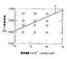
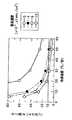
図1は本実施形態に適用されるシリコン結晶6中の窒素濃度(atoms/cm3)と成長条件V/Gと欠陥領域との関係を示している。また図2は本実施形態に適用されるシリコンウェーハ中の酸素濃度(atoms/cm3)と加熱温度TとOSF核の有無(×、○)との関係を示している。また図3は本実施形態に適用されるシリコンウェーハの冷却速度(゜C/秒)とシリコンウェーハ中の窒素濃度(atoms/cm3)とシリコンウェーハ内部のBMD密度(atoms/cm3)との関係を示している。また図4は本実施形態に適用されるシリコンウェーハの冷却速度(゜C/秒)とシリコンウェーハ中の窒素濃度(atoms/cm3)とシリコンウェーハ表層のDZ深さ(μm)との関係を示している。
【0075】
これら図1〜図4を従来技術との比較において説明する。
【0076】
従来技術2によればシリコン結晶6中への窒素の添加によりボイド欠陥および格子間シリコン型転位欠陥を含まない成長条件 (V/G) の範囲は拡大する。しかしこれらの関係は定量的には明らかではなかった。そこで本発明者らは、従来技術2で明らかではなかった窒素添加量と成長条件V/G と欠陥領域との定量的な関係を調査し図1に示すように明らかにした。
【0077】
図1は窒素の添加量を変えた 4 本のシリコン結晶 6(A,B,C,D) を育成し、欠陥分布の変化を調べることにより作成したものである。酸素濃度はおよそ 12.5 x10¹⁷(atoms/cm3)である。4 本のシリコン結晶6は、全て同じ成長条件にて、成長速度を連続的に減少させる条件にて育成した。窒素添加量は、結晶直胴のトップ部において 0, 6x10¹³, 1x10¹⁴, 4x10¹⁴ (atoms/cm3)となるよう融液5に添加する Si3N4量を調整した。シリコン結晶6中の窒素濃度は、偏析効果により結晶のボトム側に向かうほど増加する。図1の横軸は窒素濃度であり、横軸は窒素無添加結晶における臨界 (V/G)cri で規格化した成長条件 V/G を表す。ここで、(V/G)cri は結晶中心において OSF リングが閉じる、つまり消滅する臨界速度を温度勾配 G で割った値である。図1中に書き込まれた点線は、各シリコン結晶A、B、C、Dのそれぞれの結晶位置における窒素濃度と成長速度を示している。それら各結晶A、B、C、Dの中心において、欠陥種が変化するポイントを調べ図1中に丸で示した。欠陥種の評価は、赤外散乱法、酸素析出熱処理後の X線トポグラフ法、酸素析出熱処理後のエッチング光学顕微鏡観察、銅デコレーション後の X 線トポグラフ法、Secco エッチング法などの併用により判定した。図1は、欠陥種が変化するポイントを結んで欠陥領域図としている。図1より、V/G を低下させると欠陥種は、ボイド→ボイドとOSF の混合領域→OSF→格子間シリコン型転位欠陥へと変化する。図1に示されたように窒素濃度 1x10¹⁴ (atoms/cm3) 以上から OSF のみの領域、つまりボイド欠陥および格子間シリコン型転位欠陥を含まない成長条件の範囲が、急激に拡大することが分かる。無欠陥領域は図1中のOSF 領域と格子間シリコン型転位欠陥領域の境界にわずかに観察されるのみで、図中に範囲として表示できるような領域には拡大されなかった。
【0078】
以上の観察結果から、窒素添加により少なくともボイド欠陥および格子間シリコン型転位欠陥が排除されたシリコン結晶6が育成される成長条件 V/G が著しく拡大されることが分かった。
【0079】
ここで従来技術1、従来技術6によればボイド欠陥および格子間シリコン型転位欠陥を排除するためには、図1の低窒素側における狭い領域の範囲に成長条件V/Gを制御しなければならず、工業的には製造が困難であった。しかし窒素を1x1014 (atoms/cm3) 以上添加して斜線で示す領域にすることにより成長条件V/Gの範囲が拡大し、製造が極めて容易となる。
【0080】
以上のように図1に示す関係を用いて、窒素添加量と成長条件 (V/G) の適正な条件範囲を選ぶことにより、ボイド欠陥および格子間シリコン型転位欠陥を排除したシリコン結晶6を安価に、工業的に容易に製造することができるようになる。
【0081】
しかし図1によれば、窒素の添加によりボイド欠陥および格子間シリコン型転位欠陥の発生を排除した V/G 条件においては、高密度の OSF が発生し、そのままではデバイス用基板として使用するには不適切な結晶となる。
【0082】
そこで本発明者らは、図2に示す関係を見いだした。すなわち窒素添加により高密度に OSF を発生させる核を有するシリコン結晶6に、RTA 処理により適切な高温加熱を加えると OSF 核が消去されることを見出した。
【0083】
窒素添加により生じた OSF 核は極めて安定であり、通常の酸素析出核を非顕在化させるのに充分な加熱条件によっては容易に消去できない。RTA により高温加熱を行うと、その後の熱処理に伴う OSF の発生自体は抑制されるが、核を消去することは容易ではない。そして核がデバイス回路が作成される表層付近に残留すると、デバイスの機能を阻害するBMDの核として作用する。本発明者らは、シリコンウェーハの酸素濃度と OSF 核を除去するのに必要な RTA における加熱温度Tとの関係を明らかにした。まず窒素を 6 x10¹⁴ (atoms/cm3) 添加し、ウェーハ面内全面に OSF を発生する成長条件において、種々の酸素濃度のシリコン結晶6を作製した。それらのシリコン結晶6から採取したシリコンウェーハを RTA にて、種々の温度まで 100 ℃/秒にて急速昇温し、30 秒間その温度に保持し、1℃/秒にて降温した。雰囲気は Ar である。そして、800 ℃ x 4 時間 + 1000 ℃ x 16 時間の熱処理を施した後、BMD の深さ方向の分布を調べた。OSF 核が RTA の加熱により消去されていない条件においては、核はシリコンウェーハの表層付近まで残るため BMD を含まないところの所謂 DZ 層は形成されない。
【0084】
図2は、シリコンウェーハの酸素濃度を横軸とし、縦軸を RTA での加熱温度Tとした時の DZ 層が 10 ミクロン以下となる場合の条件を X印 とし、10 ミクロン以上となる条件を ○ 印として示したものである。X の領域では、OSF 核がRTA の加熱により消去されておらず、○ の領域では消去されたことを意味する。その境界を図中に直線Lで示した。この直線Lは T(℃) = 1054 + 15x110−17 x 酸素濃度 (atoms/cm3)なる式により表された。ここで酸素濃度は、FTIR により測定した酸素の吸収係数を ASTM F−121, 1979 の方法で酸素濃度に換算した値である。シリコン中の酸素析出物に対して飽和する酸素の平衡濃度と温度の関係には種々の報告値があるが、図2中の直線Lは、文献(R.A. Craven,Semiconductor Silicon, ed. H.R.Huff, ECS, Pennington N.J. 1981, P. 254) により報告された酸素の溶解度に近い値となった。一般に、酸素析出核はその結晶の酸素濃度により定まる平衡溶解温度よりかなり低温において、溶解・消滅または非顕在化するが、窒素添加のシリコン結晶6において OSF 核を消去するためには、平衡溶解温度より高温に加熱する必要があることがわかる。
【0085】
以上のように図1の斜線のOSF領域のシリコン結晶6から採取したシリコンウェーハを、図2に示す適切な条件で RTA 処理した場合には、ボイド欠陥、格子間シリコン型転位欠陥、OSFという三種のグローイン欠陥を含ませないようにすることができる。
【0086】
なお図5は図2に関連して窒素濃度がOSF核の析出に与える影響を示したものである。
【0087】
図5(a)は、1250゜C×30秒間の高温加熱をした後1゜C/秒で冷却しその後 1000 ℃ x 16 時間の熱処理を施した場合における酸素濃度と窒素濃度とOSF核析出の有無との関係を示したものである。同様に図5(b)は、1280゜C×30秒間の高温加熱をした後1゜C/秒で冷却しその後 1000 ℃ x 16時間の熱処理を施した場合における酸素濃度と窒素濃度とOSF核析出の有無との関係を示したものである。いずれの場合も窒素濃度が大きくなるに伴いOSF核が消去されにくくなっているのがわかる。これは図2において窒素濃度が高くなるに伴い直線Lが図中上方に移行することに相当する。
【0088】
また本発明者らは、RTA における急冷条件を適切に制御することにより、シリコンウェーハのBMD 密度の深さ方向分布を適切に制御することができることを見出した。それは図3、図4に示される。
【0089】
従来技術7は、窒素を添加したシリコンウェーハを RTA 処理した場合、無添加の場合よりも DZ 層が浅くなるという技術水準に留まる。図4によればDZ 層は、窒素濃度にも依存するがRTA 処理における冷却速度を調整することで制御できることが明らかになった。また図3によればウェーハ内部のBMD密度は、同じく窒素濃度にも依存するがRTA 処理における冷却速度を調整することで制御できることが明らかになった。このように窒素濃度に応じて適切な冷却速度を選定、調整することによりDZ深さ、内部BMD密度を制御でき、充分な DZ 深さを得、かつ内部 BMDを十分な高密度にすることができる。
【0090】
以下実施形態のシリコンウェーハ製造方法の手順について説明する。
【0091】
(シリコン結晶製造工程)
上述した図1の装置によってシリコン結晶6が製造される。ここで図1に示す関係にしたがい、シリコン結晶6中の窒素の添加量と成長条件 (V/G) の適正な条件範囲を選び、ボイド欠陥および格子間シリコン型転位欠陥が排除されOSFを含むシリコン結晶6が製造される。すなわち図1に斜線で示すOSF領域になるようにシリコン結晶6中の窒素の濃度と成長条件V/Gが制御される。シリコン結晶6には窒素が1×1014atoms/cm3 以上添加される。
【0092】
図1に斜線で示すOSF領域になるよう制御しているので、ボイド欠陥および格子間シリコン型転位欠陥を排除できる成長条件V/Gの範囲が広がり安価に、工業的に容易にシリコン結晶6を製造することができる。
【0093】
実験では以下の条件でシリコン結晶6を育成した。
【0094】
・窒素濃度: 4x10¹⁴ 、 6x10¹⁴ 、1x10¹⁵(atoms/cm3)
・酸素濃度: 12.5x10¹⁷(atoms/cm3)
・成長条件:(V/G)/(V/G)cri = 1.0
(V/G)cri は、図6の成長装置の育成条件において成長速度を低下させた時、窒素無添加結晶の結晶中心において OSF リングが閉じる、つまり消滅する速度を温度勾配で割った値である。上記実験の条件で得られたシリコン結晶6から採取したシリコンウェーハには、ボイド欠陥および格子間シリコン型転位欠陥は観察されず、800 ℃ x 4 時間 + 1000 ℃ x 16 時間の酸化性雰囲気での熱処理を施すことによりウェーハ全面にOSF が観察された。
【0095】
(シリコンウェーハ採取工程)
つぎに図6の製造装置によって製造されたシリコン結晶6のインゴットは、切断装置によって切断されて、シリコンウェーハが採取される。
【0096】
(加熱工程)
つぎにRTA装置を用いてランプアニールによってシリコンウェーハが図2に示す関係にしたがい高温熱処理される。
【0097】
すなわち図2に示すように、シリコンウェーハが直線L以上の領域、つまり「T=1054+15×10−17 ×酸素濃度(atoms/cm3)」(゜C)で定まる加熱温度T以上まで昇温される。これにより図2における○印で示す領域となり、シリコンウェーハに含まれるOSF核が熔解され消去される。このように窒素添加により生じた高密度の OSF 核がRTA 処理により消去される。
【0098】
またランプ炉などを用いてシリコンウェーハをランプアニールしているので、シリコンウェーハの周囲を高い温度にする必要がなくシリコンウェーハのみをランプからの熱放射によって集中的に加熱することができる。このため熱容量が小さくなり短時間で急速に昇温でき短時間で急速に冷却することができる。加熱が短時間で済むため、シリコンウェーハの金属汚染を少なくすることができる。また短時間で冷却が行われるのでシリコンウェーハ中の空孔を大量に凍結することができウェーハ内部のBMD密度を高密度にすることができる。
【0099】
実験ではシリコンウェーハを100℃/秒の昇温速度にて1250℃まで加熱し、その温度で 30 秒保持した。
【0100】
(冷却工程)
つぎに高温Tまで昇温されたシリコンウェーハが冷却される。ここで図3、図4に示す関係にしたがい冷却速度が制御されて、BMD 密度の深さ方向分布が適切に制御される。冷却速度の制御は、ランプアニールに用いられるランプ加熱器の加熱量の低減度合いを調整することにより行われる。
【0101】
冷却の過程で、高温時に大量に発生した空孔はシリコンウェーハの内部で凍結する。しかしシリコンウェーハの表層では空孔は拡散する。空孔は酸素析出を促進させる。このためシリコンウェーハの表層では酸素析出物たるBMDは発生せず、シリコンウェーハの内部では重金属のゲッタリング源になるBMDが高密度に発生する。
【0102】
図3に示す関係にしたがい、シリコンウェーハ中の窒素濃度に応じて冷却速度が制御される。これによりシリコンウェーハのうち表層のデバイス作成層を除くシリコン基板内部のBMD密度が108 atoms/cm3 以上になる。シリコンウェーハの内部(シリコン基板内部)のBMD密度が108 atoms/cm3以上になると、デバイスの製造工程中に侵入した重金属をBMDにより必要十分にゲッタリングすることができ、シリコンウェーハが高品質なものとなる。
【0103】
また図4に示す関係にしたがい、シリコンウェーハ中の窒素濃度に応じて冷却速度が制御される。これによりシリコンウェーハのうち表層のBMDが含まれないDZ深さが10μm以上になる。シリコンウェーハの表層のDZ深さが10μm以上になると、無欠陥のデバイス作成層を必要十分に確保することができる。
【0104】
図3に示す関係によれば冷却速度が大きくなるほどBMD密度がより高くなり、デバイスの製造工程中に侵入した重金属を捕獲する能力をより大きくすることができる。一方、図4に示す関係によれば冷却速度が小さくなるほどDZ深さがより深くなり無欠陥のデバイス作成層をより深く確保することができる。このように図3、図4の冷却速度は相反する関係にある。
【0105】
そこで冷却速度として1〜50゜C/秒の範囲で制御することが望ましい。この範囲の冷却速度で冷却すれば、シリコンウェーハ内部のBMD密度を所定密度以上にして必要十分な重金属ゲッタリング能力を得ることができるとともにDZ深さを所定深さ以上にして必要十分な深さの無欠陥デバイス作成層を確保することができる。
【0106】
実験では以下の冷却速度で冷却した。
【0107】
・1, 5, 10, 15, 20, 30, 50, 70 ℃/秒
ただし雰囲気は Ar である。このような速度で冷却した後、800 ℃ x 4 時間 + 1000 ℃ x 16 時間の熱処理を施し、発生した BMD の密度の深さ方向分布をエッチング法により評価した。
【0108】
図3に示す関係から、ウェーハ内部にデバイス用ウェーハとして好ましい 108 atoms/cm3 以上の密度のBMD を形成するには、冷却速度が 1 ℃/秒以上である必要があることがわかる。
【0109】
また図4に示す関係から、デバイスが形成される10ミクロンの深さ以上の DZ 深さを得るためには、窒素濃度に応じて 25〜50 ℃/秒以下の冷却速度とする必要があることがわかる。このため冷却速度は 1〜50 ℃/秒の範囲である必要がある。また窒素濃度如何にかかわらずに冷却速度のみを考慮した場合には、5〜25 ℃/秒の冷却速度で冷却することが推奨される。
【0110】
以上のように本実施形態によれば、ウェーハ内部に高密度の BMD を有し、表層のデバイス作成層をBMD もグローイン欠陥も含まない無欠陥層にしたシリコンウェーハを安価に、工業的に容易に製造できるようになる。
【0111】
なお上述した(加熱工程)でシリコンウェーハを加熱処理するにあたり、予めシリコンウェーハ上にシリコン酸化膜(SiO2)を形成しておいてもよい。
【0112】
また実施形態では、純 Ar 雰囲気で処理が行われる場合について説明した。しかし雰囲気は純 Ar 以外にも、Ar + N2 混合ガス、N2 + 微量の O2 ガスであってもよい。雰囲気に窒素を混合すると、ウェーハ内部の BMD が増加し、かつ DZ深さが減少することは良く知られている。また雰囲気に酸素を添加すると逆にウェーハ内部のBMD が減少し、かつ DZ 深さが増加することも公知である。 そこでこれらの現象を利用して、雰囲気に応じて、ウェーハ内部の BMD密度およびDZ 深さを調整することができる。
【0113】
また本実施形態では、RTA装置の加熱条件(加熱温度T、加熱時間)として1250℃ x 30 秒の場合を例示したが、これに限定されるわけではない。加熱温度Tおよび時間を適宜調整することにより、ウェーハ内部の BMD の密度および DZ 深さを所望の値に制御することができる。
【図面の簡単な説明】
【図1】図1は実施形態に適用されるシリコン結晶6中の窒素濃度(atoms/cm3)と成長条件V/Gと欠陥領域との関係を示す図である。
【図2】図2は実施形態に適用されるシリコンウェーハ中の酸素濃度(atoms/cm3)と加熱温度TとOSF核の有無(×、○)との関係を示す図である。
【図3】図3は実施形態に適用されるシリコンウェーハの冷却速度(゜C/秒)とシリコンウェーハ中の窒素濃度(atoms/cm3)とシリコンウェーハ内部のBMD密度(atoms/cm3)との関係を示す図である。
【図4】図4は実施形態に適用されるシリコンウェーハの冷却速度(゜C/秒)とシリコンウェーハ中の窒素濃度(atoms/cm3)とシリコンウェーハ表層のDZ深さ(μm)との関係を示す図である。
【図5】図5は図2に関連して窒素濃度がOSF核の析出に与える影響を示した図であり、図5(a)は、1250゜C×30秒間の高温加熱をした後1゜C/秒で冷却しその後 1000 ℃ x 16 時間の熱処理を施した場合における酸素濃度と窒素濃度とOSF核析出の有無との関係を示した図で、図5(b)は、1280゜C×30秒間の高温加熱をした後1゜C/秒で冷却しその後 1000 ℃ x 16 時間の熱処理を施した場合における酸素濃度と窒素濃度とOSF核析出の有無との関係を示した図である。
【図6】図6は実施形態のシリコンウェーハ製造方法に用いられるシリコン結晶製造装置(単結晶シリコン成長装置)の構成の一例を示した図である。
【符号の説明】
6 シリコン結晶(単結晶シリコン)[0001]
BACKGROUND OF THE INVENTION
The present invention relates to a method for manufacturing a silicon wafer, and particularly includes a high-density BMD capable of gettering a heavy metal only inside a silicon substrate excluding a surface device creation layer by eliminating void defects and interstitial silicon-type dislocation defects. The present invention relates to a manufacturing method capable of easily manufacturing a silicon wafer industrially.
[0002]
[Prior art]
Silicon crystals are produced by pulling and growing by CZ (Czochralski method). However, crystal defects called “Grow-in defects” (defects introduced during crystal growth) occur during the crystal growth process.
[0003]
In recent years, with the progress of high integration and miniaturization of semiconductor circuits, it is no longer allowed for such a glow-in defect to exist near the surface layer of a silicon wafer in which devices are formed. For this reason, the possibility of producing defect-free crystals has been studied. The crystal defects that degrade device characteristics are the following three types of defects.
[0004]
a) Void defect (cavity) caused by aggregation of vacancies.
[0005]
b) OSF (Oxidation induced stacking fault, Oxidation Induced Stacking Fault)
c) Dislocation clusters generated by aggregation of interstitial silicon (interstitial silicon-type dislocation defects, I-defect).
[0006]
A defect-free silicon single crystal is recognized or defined as a crystal that does not contain or substantially does not contain any of the above three types of defects.
[0007]
In order to obtain a silicon wafer that does not contain glow-in defects near the surface layer on which a device circuit is formed, the following method has been devised.
[0008]
1) A defect-free single crystal ingot is manufactured by controlling crystal growth conditions.
[0009]
2) Eliminate void defects near the surface of the wafer by high-temperature annealing.
[0010]
3) A defect-free layer is grown on the wafer surface by epitaxial growth.
[0011]
(Prior art 1)
Patent Document 1 (Japanese Patent Application Laid-Open No. 8-3303161) discloses a method of 1) described above, which “produces a defect-free single crystal ingot by controlling crystal growth conditions”. That is, the growth condition V / G (V: growth rate, G: temperature gradient in the axial direction of the crystal) is controlled so that vacancies and interstitial silicon in the crystal do not become excessive, thereby producing a crystal free of defects. The invention has been described.
[0012]
However, the range of growth conditions V / G for producing defect-free single crystal ingots is in a very narrow range. For this reason, there is a problem that the crystal acquisition rate is low and the cost is high.
[0013]
(Prior art 2)
Patent Document 2 (Japanese Patent Laid-Open No. 2001-146498) describes that the range of growth conditions (V / G) that do not include void defects and interstitial silicon-type dislocation defects is expanded by adding nitrogen to silicon crystals. ing.
[0014]
However, high-density OSF is generated under the V / G condition in which generation of void defects and interstitial silicon type dislocation defects is suppressed by addition of nitrogen. For this reason, a crystal inappropriate for use as a device substrate is produced, which is not desirable.
[0015]
(Prior art 3)
In connection with the above prior art 2, the present inventors have described Non-Patent Document 1 (Japan Society of Applied Physics 2002 Spring Lecture Meeting Preliminary Collection (29a-ZK-4, Takashi Yokoyama, Shinji Togawa, Toshiaki Saishoji, Kozo Nakamura, Kashioka) Junsuke) and Non-Patent Document 2 (K. Nakamura, T. Saishoji, S. Togawa, J. Tomioka, Proceedings of Forum on The Science and Technology 200. 3 quantitatively clarified the relationship between the nitrogen concentration, the growth condition V / G, and the defect region.
[0016]
That is, Patent Document 2 shows that adding nitrogen to a silicon crystal expands the range of growth conditions V / G that do not include void defects and interstitial silicon-type dislocation defects. Was not clear. In the above
[0017]
(Prior art 4)
The above method 2) of “disappearing void defects near the surface of the wafer by high-temperature annealing” is already a known technique. In this method, a silicon wafer is sampled from a silicon crystal containing void defects grown under normal growth conditions, and the void defects in the vicinity of the surface layer of the wafer are extinguished by heat treatment for a long time at a high temperature.
[0018]
However, in order to eliminate voids, annealing for 1 hour or more is required at a high temperature around 1200 ° C. For this reason, there is a problem that heavy metal contamination harmful to the device is unavoidable and slip is likely to occur.
[0019]
(Prior art 5)
The above method 3) of “growing a defect-free layer on the wafer surface by epitaxial growth” is already a known technique.
[0020]
However, there is a problem that this method is expensive.
[0021]
In the above, the glow-in defect introduced at the time of crystal growth and the problem of the prior art regarding this glow-in defect were demonstrated.
[0022]
On the other hand, in the device manufacturing process, oxygen precipitates called BMD (bulk micro defect) are generated during the heat treatment. Control of BMD generation has become an important issue in the production of silicon wafers.
[0023]
That is, if the BMD is formed near the surface layer where the device circuit is created, the function of the device is hindered. However, BMD generated inside the silicon substrate effectively acts as a gettering source for capturing heavy metals that have intruded during the device manufacturing process. For this reason, there is 10 inside the silicon wafer.8Pcs / cm3It is necessary to have the above-mentioned high-density BMD, and the surface device creation layer (10 microns) does not contain BMD and the above-mentioned glow-in defect. It is highly desirable to achieve the production easily industrially.
[0024]
(Prior art 6)
In Patent Document 3 (WO 98/45507) and Patent Document 4 (Japanese Patent Publication No. 2001-509319), the void defect existing region is reduced only to the region near the crystal center by controlling the growth condition V / G. A silicon crystal is manufactured, and a silicon wafer collected from the silicon crystal is used for a rapid rapid temperature and high temperature annealing (RTA) treatment using a lamp furnace or the like, and the wafer has a high-density BMD. In the device surface layer of the wafer surface, an invention is described in which a silicon wafer that does not contain BMD is formed.
[0025]
However, the RTA process can control the BMD generated during the heat treatment process in the device manufacturing process, but the glow-in defect cannot be eliminated.
[0026]
For this reason, in
[0027]
(Prior art 7)
A layer not including BMD on the surface layer of the silicon wafer is called a DZ layer.
[0028]
Non-Patent Document 3 (Japan Society of Applied Physics 2001 Spring Meeting Proceedings (28a-S-5))
It is described that when a silicon wafer added with nitrogen is subjected to RTA treatment, the DZ layer becomes shallower than when an additive-free silicon wafer is subjected to RTA treatment.
[0029]
[Problems to be solved by the invention]
As described above, according to the prior art, a high density (108Pcs / cm3The method of manufacturing a silicon wafer that does not contain BMD or glow-in defects inexpensively and industrially has not yet been established for the device creation layer (10 microns or more).
[0030]
Accordingly, the present invention solves the problem that a silicon wafer having a high-density BMD inside the wafer and containing no BMD or glow-in defect in the surface device creation layer can be easily and inexpensively manufactured industrially. It is to be an issue.
[0031]
[Means, actions and effects for solving the problems]
The first invention is
Controlling the concentration of nitrogen in the silicon crystal and the growth condition V / G (V: growth rate, G: axial temperature gradient of the crystal) eliminates void defects and interstitial silicon-type dislocation defects, and OSF (oxygen-induced stacking) A silicon crystal manufacturing process for manufacturing a silicon crystal including defects),
A silicon wafer collecting step of collecting a silicon wafer from the silicon crystal;
Heating the silicon wafer to a heating temperature corresponding to the oxygen concentration in the silicon wafer to erase OSF nuclei contained in the silicon wafer;
A cooling process for cooling the silicon wafer at a predetermined cooling rate;
It is the manufacturing method of the silicon wafer containing this.
[0032]
The second invention is
Controlling the concentration of nitrogen in the silicon crystal and the growth condition V / G (V: growth rate, G: axial temperature gradient of the crystal) eliminates void defects and interstitial silicon-type dislocation defects, and OSF (oxygen-induced stacking) A silicon crystal manufacturing process for manufacturing a silicon crystal including defects),
A silicon wafer collecting step of collecting a silicon wafer from the silicon crystal;
Heating the silicon wafer to a heating temperature corresponding to the oxygen concentration in the silicon wafer to erase OSF nuclei contained in the silicon wafer;
The silicon wafer is cooled at a cooling rate corresponding to the nitrogen concentration in the silicon wafer, and the BMD (bulk fine defect) density inside the silicon substrate excluding the surface device creation layer of the silicon wafer is 108Atoms / cm3More cooling process
It is the manufacturing method of the silicon wafer containing this.
[0033]
The third invention is
Controlling the concentration of nitrogen in the silicon crystal and the growth condition V / G (V: growth rate, G: axial temperature gradient of the crystal) eliminates void defects and interstitial silicon-type dislocation defects, and OSF (oxygen-induced stacking) A silicon crystal manufacturing process for manufacturing a silicon crystal including defects),
A silicon wafer collecting step of collecting a silicon wafer from the silicon crystal;
Heating the silicon wafer to a heating temperature corresponding to the oxygen concentration in the silicon wafer to erase OSF nuclei contained in the silicon wafer;
A cooling step in which the silicon wafer is cooled at a cooling rate corresponding to the nitrogen concentration in the silicon wafer, and the DZ depth not including BMD (bulk fine defects) on the surface layer of the silicon wafer is 10 μm or more;
It is the manufacturing method of the silicon wafer containing this.
[0034]
The fourth invention is
Controlling the concentration of nitrogen in the silicon crystal and the growth condition V / G (V: growth rate, G: axial temperature gradient of the crystal) eliminates void defects and interstitial silicon-type dislocation defects, and OSF (oxygen-induced stacking) A silicon crystal manufacturing process for manufacturing a silicon crystal including defects),
A silicon wafer collecting step of collecting a silicon wafer from the silicon crystal;
Heating the silicon wafer to a heating temperature corresponding to the oxygen concentration in the silicon wafer to erase OSF nuclei contained in the silicon wafer;
The silicon wafer is cooled at a cooling rate corresponding to the nitrogen concentration in the silicon wafer, and the BMD (bulk fine defect) density inside the silicon substrate excluding the surface device creation layer of the silicon wafer is 108atoms / cm3In addition to the above, a cooling step in which the DZ depth not including the surface BMD is 10 μm or more;
It is the manufacturing method of the silicon wafer containing this.
[0035]
The fifth invention
Controlling the concentration of nitrogen in the silicon crystal and the growth condition V / G (V: growth rate, G: axial temperature gradient of the crystal) eliminates void defects and interstitial silicon-type dislocation defects, and OSF (oxygen-induced stacking) A silicon crystal manufacturing process for manufacturing a silicon crystal including defects),
A silicon wafer collecting step of collecting a silicon wafer from the silicon crystal;
Heating the silicon wafer to a heating temperature corresponding to the oxygen concentration in the silicon wafer to erase OSF nuclei contained in the silicon wafer;
The silicon wafer is cooled at a cooling rate of 1 to 50 ° C./second so that the BMD (bulk fine defect) density inside the silicon substrate excluding the device creation layer on the surface layer of the silicon wafer exceeds a predetermined density. A cooling step of making the DZ depth not including BMD a predetermined depth or more;
It is the manufacturing method of the silicon wafer containing this.
[0036]
The sixth invention is the first invention, the second invention, the third invention, the fourth invention, the fifth invention,
In the silicon crystal manufacturing process, 1 × 10 nitrogen is added to the silicon crystal.14atoms / cm3Add more
It is characterized by.
[0037]
The seventh invention is the first invention, the second invention, the third invention, the fourth invention, the fifth invention,
In the heating step, the silicon wafer is “T = 1054 + 15 × 10.-17
× Oxygen concentration (atoms / cm3) ”(Temperature higher than heating temperature T determined by ° C)
It is characterized by.
[0038]
The eighth invention is the first invention, the second invention, the third invention, the fourth invention, the fifth invention,
In the heating step, the silicon wafer is subjected to high-temperature heat treatment by lamp annealing.
It is characterized by.
[0039]
A ninth invention is the fourth invention,
In the cooling step, the silicon wafer is cooled at a cooling rate of 1 to 50 ° C./second.
It is characterized by.
[0040]
According to the first invention, the concentration of nitrogen in the silicon crystal and the growth condition V / G (V: growth rate, G: axial temperature gradient of the crystal) are controlled so that the OSF region indicated by hatching in FIG. Is done. As a result, void defects and interstitial silicon-type dislocation defects are eliminated, and a silicon crystal containing OSF (oxygen-induced stacking fault) is manufactured.
[0041]
Next, a silicon wafer is collected from the manufactured silicon crystal.
[0042]
Next, for example, by lamp annealing, the silicon wafer is heated to a heating temperature T corresponding to the oxygen concentration in the silicon wafer so that the region indicated by a circle in FIG. 2 is obtained. Thereby, the OSF nucleus contained in the silicon wafer is melted and erased.
[0043]
Next, by controlling a lamp heater used for lamp annealing, for example, as shown in FIGS. 3 and 4, the silicon wafer is cooled at a predetermined cooling rate. During the cooling process, vacancies generated in large quantities at high temperatures (holes in which silicon has escaped from normal positions on the lattice) are frozen inside the silicon wafer. However, vacancies diffuse on the surface of the silicon wafer. The vacancies promote oxygen precipitation. For this reason, BMD which is an oxygen precipitate is not generated on the surface layer of the silicon wafer, and BMD which is a heavy metal gettering source is generated at a high density inside the silicon wafer.
[0044]
As described above, the OSF region indicated by the oblique lines in FIG. 1 is controlled, so that the range of growth conditions V / G that can eliminate void defects and interstitial silicon-type dislocation defects is widened, and the silicon crystal is easily industrialized at low cost. Can be manufactured. In this silicon crystal manufacturing process, void defects and interstitial silicon-type dislocation defects are eliminated from the glow-in defects. Further, since the silicon wafer is heated to the heating temperature T corresponding to the oxygen concentration in the silicon wafer so as to be the region indicated by the circle in FIG. 2, the OSF nucleus that generates the OSF among the glow-in defects is erased. be able to. Also, as shown in FIGS. 3 and 4, since the silicon wafer is cooled from a high temperature at a predetermined cooling rate, the device creation layer on the surface layer of the silicon wafer should be a defect-free layer that does not include BMD or glow-in defects. Thus, a high-density BMD serving as a heavy metal gettering source can be generated only inside the silicon wafer.
[0045]
As described above, according to the first invention, a silicon wafer having a high-density BMD inside the wafer and having a surface device creation layer as a defect-free layer containing neither BMD nor glow-in defects is inexpensive and easily industrially available. Can be manufactured.
[0046]
The second invention is obtained by adding a technical limitation to the cooling process of the first invention. As shown in FIG. 3, by controlling the cooling rate according to the nitrogen concentration in the silicon wafer, The BMD density inside the silicon substrate excluding the surface device creation layer is 108Atoms / cm3More than that. BMD density inside silicon wafer (inside silicon substrate) is 108Atoms / cm3If it becomes above, the heavy metal which penetrate | invaded during the manufacturing process of a device will be gettered sufficiently by BMD, and a high quality silicon wafer will be created.
[0047]
In the third invention, a technical limitation is added to the cooling process of the first invention. As shown in FIG. 4, by controlling the cooling rate according to the nitrogen concentration in the silicon wafer, The DZ depth not including the BMD of the surface layer is set to 10 μm or more. When the DZ depth of the surface layer of the silicon wafer is 10 μm or more, a defect-free device creation layer can be ensured sufficiently.
[0048]
The fourth invention is obtained by adding technical limitations to the cooling process of the first invention. As shown in FIGS. 3 and 4, silicon is controlled by controlling the cooling rate according to the nitrogen concentration in the silicon wafer. The BMD density inside the silicon substrate excluding the surface device creation layer of the wafer is 108Atoms / cm3In addition to the above, the DZ depth not including the surface BMD of the silicon wafer is set to 10 μm or more.
[0049]
According to the fourth invention, the heavy metal that has entered during the device manufacturing process is sufficiently and sufficiently gettered by the BMD to produce a high-quality silicon wafer, and a defect-free device creation layer can be secured sufficiently. it can.
[0050]
The fifth invention is obtained by adding technical limitations to the cooling process of the first invention. As shown in FIGS. 3 and 4, the silicon wafer is cooled at a cooling rate of 1 to 50 ° C./second. That is, as shown in FIG. 3, the higher the cooling rate, the higher the BMD density and the greater the ability to capture heavy metals that have entered during the device manufacturing process. On the other hand, as shown in FIG. 4, as the cooling rate decreases, the DZ depth can be increased, and a defect-free device creation layer can be secured more deeply. As described above, the cooling rates in FIGS. 3 and 4 are contradictory to each other. However, if the cooling rate is set to 1 to 50 ° C./second, the BMD density inside the silicon wafer is increased to a predetermined density or more and a necessary and sufficient heavy metal getter is obtained. The ring capability can be obtained, and the DZ depth can be set to a predetermined depth or more to ensure a defect-free device formation layer having a necessary and sufficient depth.
[0051]
In the sixth aspect of the present invention, a technical limitation is added to the silicon crystal manufacturing process of the first to fifth aspects of the invention. As shown in FIG.14atoms / cm3More than that is added. As a result, as shown by hatching in FIG. 1, the range of growth conditions V / G that can eliminate void defects and interstitial silicon-type dislocation defects is widened, and a silicon crystal can be easily produced industrially at low cost. .
[0052]
In the seventh invention, the heating process of the first invention to the fifth invention is technically limited. As shown in FIG. 2, the silicon wafer has a structure of “T = 1054 + 15 × 10”.-17X Oxygen concentration (atoms / cm3) ”(° C.) or higher. As a result, an area indicated by a circle marked with a straight line L or higher in FIG.
[0053]
In the eighth invention, a technical limitation is added to the heating process of the first invention to the fifth invention, and the silicon wafer is subjected to high-temperature heat treatment by lamp annealing. That is, if the silicon wafer is lamp annealed using a lamp furnace or the like, it is not necessary to raise the temperature around the silicon wafer, and only the silicon wafer can be heated intensively by the heat radiation from the lamp. For this reason, the heat capacity becomes small, the temperature can be increased rapidly in a short time, and the cooling can be rapidly performed in a short time. Since heating can be completed in a short time, metal contamination of the silicon wafer can be reduced. Further, since cooling is performed in a short time, a large number of holes in the silicon wafer can be frozen, and the BMD density inside the wafer can be increased.
[0054]
In the ninth invention, a technical limitation is added to the cooling process of the fourth invention, and the silicon wafer is cooled at a cooling rate of 1 to 50 ° C./second. The ninth invention is a combination of the fourth invention and the fifth invention, and as shown in FIGS. 3 and 4, cooling is performed at a cooling rate of 1 to 50 ° C./second depending on the nitrogen concentration in the silicon wafer. As a result, the BMD density inside the silicon substrate excluding the surface device creation layer of the silicon wafer is 108Atoms / cm3In addition to the above, the DZ depth not including the surface BMD of the silicon wafer is set to 10 μm or more.
[0055]
DETAILED DESCRIPTION OF THE INVENTION
Embodiments of a silicon wafer manufacturing method according to the present invention will be described below with reference to the drawings.
[0056]
FIG. 6 is a side view of an example of the configuration of the silicon crystal manufacturing apparatus used in the embodiment.
[0057]
As shown in FIG. 6, a single
[0058]
In the CZ furnace 2, there is provided a quartz crucible 3 for melting a polycrystalline silicon raw material and storing it as a melt 5. The quartz crucible 3 is covered with a
[0059]
A
[0060]
A pulling
[0061]
Polycrystalline silicon (Si) is heated and melted in the quartz crucible 3. When the temperature of the melt 5 is stabilized, the pulling
[0062]
In this embodiment, in order to add nitrogen to the
[0063]
The rotating
[0064]
By shutting off the inside of the CZ furnace 2 and the outside air, the inside of the furnace 2 is maintained in a vacuum (for example, about 20 Torr). That is, argon gas 7 as an inert gas is supplied to the CZ furnace 2 and is exhausted from the exhaust port of the CZ furnace 2 by a pump. Thereby, the inside of the furnace 2 is depressurized to a predetermined pressure.
[0065]
Various evaporants are generated in the CZ furnace 2 during the single crystal pulling process (one batch). Therefore, the argon gas 7 is supplied to the CZ furnace 2 and exhausted together with the evaporated substance outside the CZ furnace 2 to remove the evaporated substance from the CZ furnace 2 and clean it. The supply flow rate of the argon gas 7 is set for each process in one batch.
[0066]
As the
[0067]
Above the quartz crucible 3 and around the
[0068]
The
[0069]
The growth condition V / G (V: growth rate, G: axial temperature gradient of the crystal) of the
[0070]
Also, by adjusting the amount of nitrogen introduced into the quartz crucible 3, the concentration of nitrogen in the silicon crystal 6 (nitrogen addition amount, atoms / cm3) Is controlled.
[0071]
Further, during the pulling, the oxygen concentration (atoms / cm) in the
[0072]
The ingot of the
[0073]
The collected silicon wafer is subjected to lamp annealing using an apparatus (RTA apparatus) that performs rapid thermal annealing (RTA: Rapid Thermal Annealing). That is, the silicon wafer is rapidly heated to a high temperature T of 1200 ° C. or higher by heat radiation from the lamp heater, and the high temperature is maintained for a predetermined time. Subsequently, the silicon wafer is cooled at a predetermined cooling rate (° C./second) from a high temperature state by adjusting the degree of reduction of the heating amount of the lamp heater.
[0074]
FIG. 1 shows the nitrogen concentration (atoms / cm) in the
[0075]
1 to 4 will be described in comparison with the prior art.
[0076]
According to the prior art 2, the range of growth conditions (V / G) not including void defects and interstitial silicon type dislocation defects is expanded by adding nitrogen into the
[0077]
FIG. 1 is prepared by growing four silicon crystals 6 (A, B, C, D) with different amounts of nitrogen added and examining changes in defect distribution. Oxygen concentration is approximately 12.5 x10¹⁷(Atoms / cm3). The four
[0078]
From the above observation results, it was found that the growth condition V / G for growing the
[0079]
Here, according to the
[0080]
As described above, by using the relationship shown in FIG. 1 and selecting an appropriate condition range of nitrogen addition amount and growth condition (V / G),
[0081]
However, according to FIG. 1, in the V / G condition where the generation of void defects and interstitial silicon-type dislocation defects is eliminated by the addition of nitrogen, high-density OSF is generated and can be used as it is as a device substrate. Inappropriate crystals.
[0082]
Therefore, the present inventors have found the relationship shown in FIG. That is, the present inventors have found that the OSF nuclei are erased when an appropriate high-temperature heating is applied to the
[0083]
The OSF nuclei produced by the addition of nitrogen are extremely stable and cannot be easily erased by heating conditions sufficient to make the normal oxygen precipitation nuclei invisible. When high temperature heating is performed with RTA, the generation of OSF accompanying the subsequent heat treatment is suppressed, but it is not easy to erase the nucleus. When the nucleus remains in the vicinity of the surface layer where the device circuit is created, it acts as a nucleus of the BMD that inhibits the function of the device. The present inventors have clarified the relationship between the oxygen concentration of the silicon wafer and the heating temperature T in RTA necessary for removing the OSF nucleus. First, nitrogen 6 x 10¹⁴(Atoms / cm3)
[0084]
In FIG. 2, the horizontal axis is the oxygen concentration of the silicon wafer, and the vertical axis is the heating temperature T at RTA. The condition when the DZ layer is 10 microns or less is indicated by X, and the conditions for 10 microns or more are shown. ○ Shown as a mark. In the area of X, it means that the OSF nucleus was not erased by the heating of the RTA, but was erased in the area of ○. The boundary is indicated by a straight line L in the figure. This straight line L is T (° C) = 1054 + 15x110-17X Oxygen concentration (atoms / cm3). Here, the oxygen concentration is a value obtained by converting an oxygen absorption coefficient measured by FTIR into an oxygen concentration by the method of ASTM F-121, 1979. Although there are various reported values for the relationship between the equilibrium concentration of oxygen saturated with respect to the oxygen precipitates in silicon and the temperature, the straight line L in FIG. 2 represents the literature (RA Craven, Semiconductor Silicon, Ed. HR Huff, ECS, Pennington N.J. 1981, P. 254), which is close to the solubility of oxygen. In general, the oxygen precipitation nuclei dissolve, disappear, or become invisible at a temperature considerably lower than the equilibrium melting temperature determined by the oxygen concentration of the crystal. However, in order to erase the OSF nucleus in the
[0085]
As described above, when a silicon wafer taken from the
[0086]
FIG. 5 shows the effect of nitrogen concentration on the precipitation of OSF nuclei in relation to FIG.
[0087]
FIG. 5 (a) shows the oxygen concentration, nitrogen concentration, and OSF nucleation in the case of heating at 1250 ° C for 30 seconds, cooling at 1 ° C / second, and then heat-treating at 1000 ° C for 16 hours. It shows the relationship between presence and absence. Similarly, FIG. 5 (b) shows the oxygen concentration, nitrogen concentration, and OSF nucleus when heated at 1280 ° C x 30 seconds, cooled at 1 ° C / second, and then heat-treated at 1000 ° C for 16 hours. It shows the relationship with the presence or absence of precipitation. In either case, it can be seen that the OSF nuclei are less likely to be erased as the nitrogen concentration increases. This corresponds to the straight line L moving upward in FIG. 2 as the nitrogen concentration increases.
[0088]
The inventors have also found that the BMD density distribution in the depth direction of the silicon wafer can be appropriately controlled by appropriately controlling the quenching conditions in RTA. This is shown in FIGS.
[0089]
Conventional technology 7 remains at the technical level that the DTA layer becomes shallower when RTA treatment is performed on a silicon wafer to which nitrogen is added than when it is not added. According to FIG. 4, it became clear that the DZ layer can be controlled by adjusting the cooling rate in the RTA treatment although it depends on the nitrogen concentration. FIG. 3 also shows that the BMD density inside the wafer can be controlled by adjusting the cooling rate in the RTA process, although it also depends on the nitrogen concentration. In this way, by selecting and adjusting an appropriate cooling rate according to the nitrogen concentration, the DZ depth and internal BMD density can be controlled, and sufficient DZ depth can be obtained and the internal BMD can be made sufficiently dense. it can.
[0090]
The procedure of the silicon wafer manufacturing method of the embodiment will be described below.
[0091]
(Silicon crystal manufacturing process)
The
[0092]
Since the OSF region shown by hatching in FIG. 1 is controlled, the range of growth conditions V / G that can eliminate void defects and interstitial silicon type dislocation defects is widened, and the
[0093]
In the experiment, the
[0094]
・ Nitrogen concentration: 4x10¹⁴, 6x10141x1015(Atoms / cm3)
・ Oxygen concentration: 12.5x10¹⁷(Atoms / cm3)
・ Growth conditions: (V / G) / (V / G) cri = 1.0
(V / G) cri is the value obtained by dividing the rate at which the OSF ring closes, or disappears, by the temperature gradient at the crystal center of the nitrogen-free crystal when the growth rate is reduced under the growth conditions of the growth apparatus of FIG. is there. Void defects and interstitial silicon-type dislocation defects are not observed in the silicon wafer collected from the
[0095]
(Silicon wafer sampling process)
Next, the ingot of the
[0096]
(Heating process)
Next, the silicon wafer is subjected to high-temperature heat treatment according to the relationship shown in FIG. 2 by lamp annealing using an RTA apparatus.
[0097]
That is, as shown in FIG. 2, the region where the silicon wafer is not less than the straight line L, that is, “T = 1054 + 15 × 10-17X Oxygen concentration (atoms / cm3) ”(° C.), the temperature is raised to a temperature equal to or higher than the heating temperature T. As a result, a region indicated by a circle in FIG. 2 is formed, and the OSF nucleus contained in the silicon wafer is melted and erased. In this way, high-density OSF nuclei generated by nitrogen addition are erased by the RTA process.
[0098]
Further, since the silicon wafer is subjected to lamp annealing using a lamp furnace or the like, it is not necessary to raise the temperature around the silicon wafer, and only the silicon wafer can be intensively heated by the heat radiation from the lamp. For this reason, the heat capacity becomes small, the temperature can be increased rapidly in a short time, and the cooling can be rapidly performed in a short time. Since heating can be completed in a short time, metal contamination of the silicon wafer can be reduced. Further, since cooling is performed in a short time, a large number of holes in the silicon wafer can be frozen, and the BMD density inside the wafer can be increased.
[0099]
In the experiment, the silicon wafer was heated to 1250 ° C. at a temperature increase rate of 100 ° C./second, and held at that temperature for 30 seconds.
[0100]
(Cooling process)
Next, the silicon wafer heated to the high temperature T is cooled. Here, the cooling rate is controlled according to the relationship shown in FIG. 3 and FIG. 4, and the BMD density distribution in the depth direction is appropriately controlled. The cooling rate is controlled by adjusting the degree of reduction of the heating amount of the lamp heater used for lamp annealing.
[0101]
During the cooling process, a large number of vacancies generated at a high temperature are frozen inside the silicon wafer. However, vacancies diffuse on the surface of the silicon wafer. The vacancies promote oxygen precipitation. For this reason, BMD which is an oxygen precipitate is not generated on the surface layer of the silicon wafer, and BMD which is a heavy metal gettering source is generated at a high density inside the silicon wafer.
[0102]
According to the relationship shown in FIG. 3, the cooling rate is controlled according to the nitrogen concentration in the silicon wafer. As a result, the BMD density inside the silicon substrate excluding the surface device creation layer of the silicon wafer is 108Atoms / cm3That's it. BMD density inside silicon wafer (inside silicon substrate) is 108Atoms / cm3If it becomes above, the heavy metal which penetrate | invaded during the manufacturing process of a device can be gettered sufficiently and sufficiently by BMD, and a silicon wafer will become a high quality thing.
[0103]
Further, according to the relationship shown in FIG. 4, the cooling rate is controlled according to the nitrogen concentration in the silicon wafer. As a result, the DZ depth not including the surface BMD of the silicon wafer becomes 10 μm or more. When the DZ depth of the surface layer of the silicon wafer is 10 μm or more, a defect-free device creation layer can be ensured sufficiently.
[0104]
According to the relationship shown in FIG. 3, the BMD density increases as the cooling rate increases, and the ability to capture heavy metals that have intruded during the device manufacturing process can be increased. On the other hand, according to the relationship shown in FIG. 4, as the cooling rate decreases, the DZ depth becomes deeper and a deeper device-free layer can be secured. Thus, the cooling rates in FIGS. 3 and 4 are in a contradictory relationship.
[0105]
Therefore, it is desirable to control the cooling rate in the range of 1 to 50 ° C./second. By cooling at a cooling rate in this range, the BMD density inside the silicon wafer can be increased to a predetermined density or higher to obtain a necessary and sufficient heavy metal gettering capability, and the DZ depth is set to a predetermined depth or higher to obtain a necessary and sufficient depth. It is possible to secure a defect-free device formation layer.
[0106]
In the experiment, cooling was performed at the following cooling rate.
[0107]
・ 1, 5, 10, 15, 20, 30, 50, 70 ° C / second
However, the atmosphere is Ar. After cooling at such a rate, a heat treatment was performed at 800 ° C. x 4 hours + 1000 ° C. x 16 hours, and the density direction distribution of the generated BMD was evaluated by an etching method.
[0108]
From the relationship shown in FIG. 3, it is preferable as a device wafer inside the wafer. 108Atoms / cm3It can be seen that in order to form a BMD having the above density, the cooling rate needs to be 1 ° C./second or more.
[0109]
Also, from the relationship shown in FIG. 4, in order to obtain a DZ depth of 10 microns or more at which the device is formed, it is necessary to set a cooling rate of 25 to 50 ° C./second or less depending on the nitrogen concentration. I understand. For this reason, the cooling rate needs to be in the range of 1 to 50 ° C./second. When considering only the cooling rate regardless of the nitrogen concentration, it is recommended to cool at a cooling rate of 5 to 25 ° C./sec.
[0110]
As described above, according to the present embodiment, a silicon wafer having a high-density BMD inside the wafer and having a surface device creation layer as a defect-free layer containing neither BMD nor glow-in defects is inexpensive and easily industrially available. Can be manufactured.
[0111]
Note that when the silicon wafer is heat-treated in the above (heating step), a silicon oxide film (SiO 2) may be formed on the silicon wafer in advance.
[0112]
In the embodiment, the case where the processing is performed in a pure Ar atmosphere has been described. However, the atmosphere may be Ar + N2 mixed gas, N2 + trace amount O2 gas other than pure Ar. It is well known that when nitrogen is mixed in the atmosphere, the BMD inside the wafer increases and the DZ depth decreases. It is also known that when oxygen is added to the atmosphere, the BMD inside the wafer decreases and the DZ depth increases. Therefore, using these phenomena, the BMD density and the DZ depth inside the wafer can be adjusted according to the atmosphere.
[0113]
In the present embodiment, the case of 1250 ° C. × 30 seconds is exemplified as the heating condition (heating temperature T, heating time) of the RTA apparatus, but the present invention is not limited to this. By appropriately adjusting the heating temperature T and time, the BMD density and DZ depth inside the wafer can be controlled to desired values.
[Brief description of the drawings]
FIG. 1 shows a nitrogen concentration (atoms / cm) in a
FIG. 2 is a diagram illustrating an oxygen concentration (atoms / cm in a silicon wafer applied to the embodiment;3), The heating temperature T, and the presence / absence of OSF nuclei (×, ○).
FIG. 3 shows a cooling rate (° C./second) of a silicon wafer applied to the embodiment and a nitrogen concentration (atoms / cm) in the silicon wafer.3) And BMD density inside the silicon wafer (atoms / cm3FIG.
FIG. 4 shows a cooling rate (° C./second) of a silicon wafer applied to the embodiment and a nitrogen concentration (atoms / cm) in the silicon wafer.3And the DZ depth (μm) of the silicon wafer surface layer.
FIG. 5 is a diagram showing the influence of nitrogen concentration on the precipitation of OSF nuclei in relation to FIG. 2, and FIG. 5 (a) shows the result after high-temperature heating at 1250 ° C. × 30 seconds. FIG. 5 (b) shows the relationship between the oxygen concentration, nitrogen concentration, and presence / absence of OSF nucleation when cooling at ° C / second and then heat-treating at 1000 ° C for 16 hours. X is a diagram showing the relationship between oxygen concentration, nitrogen concentration, and presence / absence of OSF nucleation when heat treatment is performed at a high temperature of 30 seconds and then cooled at 1 ° C / second and then heat-treated at 1000 ° C for 16 hours. .
FIG. 6 is a diagram showing an example of the configuration of a silicon crystal manufacturing apparatus (single crystal silicon growth apparatus) used in the silicon wafer manufacturing method of the embodiment.
[Explanation of symbols]
6 Silicon crystal (single crystal silicon)
Claims (9)
Translated fromJapanese前記シリコン結晶からシリコンウェーハを採取するシリコンウェーハ採取工程と、
シリコンウェーハ中の酸素濃度に応じた加熱温度までシリコンウェーハを加熱して、シリコンウェーハに含まれるOSF核を消去する加熱工程と、
シリコンウェーハを所定の冷却速度で冷却する冷却工程と
を含むことを特徴とするシリコンウェーハの製造方法。Controlling the concentration of nitrogen in the silicon crystal and the growth condition V / G (V: growth rate, G: axial temperature gradient of the crystal) eliminates void defects and interstitial silicon-type dislocation defects, and OSF (oxygen-induced stacking) A silicon crystal manufacturing process for manufacturing a silicon crystal including defects),
A silicon wafer collecting step of collecting a silicon wafer from the silicon crystal;
Heating the silicon wafer to a heating temperature corresponding to the oxygen concentration in the silicon wafer to erase OSF nuclei contained in the silicon wafer;
And a cooling step of cooling the silicon wafer at a predetermined cooling rate.
前記シリコン結晶からシリコンウェーハを採取するシリコンウェーハ採取工程と、
シリコンウェーハ中の酸素濃度に応じた加熱温度までシリコンウェーハを加熱して、シリコンウェーハに含まれるOSF核を消去する加熱工程と、
シリコンウェーハ中の窒素濃度に応じた冷却速度でシリコンウェーハを冷却して、シリコンウェーハのうち表層のデバイス作成層を除くシリコン基板内部のBMD(バルク微細欠陥)密度を108 atoms/cm3 以上にする冷却工程と
を含むことを特徴とするシリコンウェーハの製造方法。Controlling the concentration of nitrogen in the silicon crystal and the growth condition V / G (V: growth rate, G: axial temperature gradient of the crystal) eliminates void defects and interstitial silicon-type dislocation defects, and OSF (oxygen-induced stacking) A silicon crystal manufacturing process for manufacturing a silicon crystal including defects),
A silicon wafer collecting step of collecting a silicon wafer from the silicon crystal;
Heating the silicon wafer to a heating temperature corresponding to the oxygen concentration in the silicon wafer to erase OSF nuclei contained in the silicon wafer;
The silicon wafer is cooled at a cooling rate according to the nitrogen concentration in the silicon wafer, and the BMD (bulk fine defect) density inside the silicon substrate excluding the surface device creation layer of the silicon wafer is increased to 108 atoms / cm3 or more. A method for producing a silicon wafer, comprising: a cooling step.
前記シリコン結晶からシリコンウェーハを採取するシリコンウェーハ採取工程と、
シリコンウェーハ中の酸素濃度に応じた加熱温度までシリコンウェーハを加熱して、シリコンウェーハに含まれるOSF核を消去する加熱工程と、
シリコンウェーハ中の窒素濃度に応じた冷却速度でシリコンウェーハを冷却して、シリコンウェーハの表層のBMD(バルク微細欠陥)が含まれないDZ深さを10μm以上にする冷却工程と
を含むことを特徴とするシリコンウェーハの製造方法。Controlling the concentration of nitrogen in the silicon crystal and the growth condition V / G (V: growth rate, G: axial temperature gradient of the crystal) eliminates void defects and interstitial silicon-type dislocation defects, and OSF (oxygen-induced stacking) A silicon crystal manufacturing process for manufacturing a silicon crystal including defects),
A silicon wafer collecting step of collecting a silicon wafer from the silicon crystal;
Heating the silicon wafer to a heating temperature corresponding to the oxygen concentration in the silicon wafer to erase OSF nuclei contained in the silicon wafer;
A cooling step of cooling the silicon wafer at a cooling rate according to a nitrogen concentration in the silicon wafer to make a DZ depth not including BMD (bulk fine defects) on the surface layer of the silicon wafer to 10 μm or more. A method for manufacturing a silicon wafer.
前記シリコン結晶からシリコンウェーハを採取するシリコンウェーハ採取工程と、
シリコンウェーハ中の酸素濃度に応じた加熱温度までシリコンウェーハを加熱して、シリコンウェーハに含まれるOSF核を消去する加熱工程と、
シリコンウェーハ中の窒素濃度に応じた冷却速度でシリコンウェーハを冷却して、シリコンウェーハのうち表層のデバイス作成層を除くシリコン基板内部のBMD(バルク微細欠陥)密度を108atoms/cm3以上にするとともに、表層のBMDが含まれないDZ深さを10μm以上にする冷却工程と
を含むことを特徴とするシリコンウェーハの製造方法。Controlling the concentration of nitrogen in the silicon crystal and the growth condition V / G (V: growth rate, G: axial temperature gradient of the crystal) eliminates void defects and interstitial silicon-type dislocation defects, and OSF (oxygen-induced stacking) A silicon crystal manufacturing process for manufacturing a silicon crystal including defects),
A silicon wafer collecting step of collecting a silicon wafer from the silicon crystal;
Heating the silicon wafer to a heating temperature corresponding to the oxygen concentration in the silicon wafer to erase OSF nuclei contained in the silicon wafer;
The silicon wafer is cooled at a cooling rate according to the nitrogen concentration in the silicon wafer, and the BMD (bulk fine defect) density inside the silicon substrate excluding the surface device creation layer of the silicon wafer is increased to 108 atoms / cm3 or more. And a cooling step of making the DZ depth not including the surface layer BMD 10 μm or more.
前記シリコン結晶からシリコンウェーハを採取するシリコンウェーハ採取工程と、
シリコンウェーハ中の酸素濃度に応じた加熱温度までシリコンウェーハを加熱して、シリコンウェーハに含まれるOSF核を消去する加熱工程と、
シリコンウェーハを1〜50゜C/秒の冷却速度で冷却して、シリコンウェーハのうち表層のデバイス作成層を除くシリコン基板内部のBMD(バルク微細欠陥)密度を所定密度以上にするとともに、表層のBMDが含まれないDZ深さを所定深さ以上にする冷却工程と
を含むことを特徴とするシリコンウェーハの製造方法。Controlling the concentration of nitrogen in the silicon crystal and the growth condition V / G (V: growth rate, G: axial temperature gradient of the crystal) eliminates void defects and interstitial silicon-type dislocation defects, and OSF (oxygen-induced stacking) A silicon crystal manufacturing process for manufacturing a silicon crystal including defects),
A silicon wafer collecting step of collecting a silicon wafer from the silicon crystal;
Heating the silicon wafer to a heating temperature corresponding to the oxygen concentration in the silicon wafer to erase OSF nuclei contained in the silicon wafer;
The silicon wafer is cooled at a cooling rate of 1 to 50 ° C./second so that the BMD (bulk fine defect) density inside the silicon substrate excluding the device creation layer on the surface layer of the silicon wafer exceeds a predetermined density. And a cooling step of setting a DZ depth not including BMD to a predetermined depth or more.
を特徴とする請求項1、2、3、4、5に記載のシリコンウェーハの製造方法。6. The method of manufacturing a silicon wafer according to claim 1, wherein 3, in the silicon crystal manufacturing process, nitrogen is added to the silicon crystal in an amount of 1 × 10¹⁴ atoms / cm3 or more.
を特徴とする請求項1、2、3、4、5に記載のシリコンウェーハの製造方法。In the heating step, the silicon wafer is heated to a temperature equal to or higher than a heating temperature T determined by “T = 1054 + 15 × 10−17 × oxygen concentration (atoms / cm3 )” (° C.). 3. A method for producing a silicon wafer according to 3, 4, and 5.
を特徴とする請求項1、2、3、4、5に記載のシリコンウェーハの製造方法。6. The method of manufacturing a silicon wafer according to claim 1, wherein in the heating step, the silicon wafer is subjected to high temperature heat treatment by lamp annealing.
を特徴とする請求項4記載のシリコンウェーハの製造方法。5. The method of manufacturing a silicon wafer according to claim 4, wherein in the cooling step, the silicon wafer is cooled at a cooling rate of 1 to 50 [deg.] C./second.
Priority Applications (1)
| Application Number | Priority Date | Filing Date | Title |
|---|---|---|---|
| JP2002273571AJP4605626B2 (en) | 2002-09-19 | 2002-09-19 | Silicon wafer manufacturing method |
Applications Claiming Priority (1)
| Application Number | Priority Date | Filing Date | Title |
|---|---|---|---|
| JP2002273571AJP4605626B2 (en) | 2002-09-19 | 2002-09-19 | Silicon wafer manufacturing method |
Publications (2)
| Publication Number | Publication Date |
|---|---|
| JP2004111732Atrue JP2004111732A (en) | 2004-04-08 |
| JP4605626B2 JP4605626B2 (en) | 2011-01-05 |
Family
ID=32270294
Family Applications (1)
| Application Number | Title | Priority Date | Filing Date |
|---|---|---|---|
| JP2002273571AExpired - LifetimeJP4605626B2 (en) | 2002-09-19 | 2002-09-19 | Silicon wafer manufacturing method |
Country Status (1)
| Country | Link |
|---|---|
| JP (1) | JP4605626B2 (en) |
Cited By (11)
| Publication number | Priority date | Publication date | Assignee | Title |
|---|---|---|---|---|
| WO2005104208A1 (en)* | 2004-04-23 | 2005-11-03 | Komatsu Electronic Metals Co., Ltd. | Silicon semiconductor substrate heat-treatment method and silicon semiconductor substrate treated by the method |
| JP2006066913A (en)* | 2004-08-26 | 2006-03-09 | Siltronic Ag | Semiconductor wafer having a layer structure exhibiting low Warp and Bow and method for manufacturing the same |
| WO2006103837A1 (en)* | 2005-03-28 | 2006-10-05 | Komatsu Denshi Kinzoku Kabushiki Kaisha | Process for producing silicon single-crystal, annealed wafer and process for producing annealed wafer |
| JP2010267846A (en)* | 2009-05-15 | 2010-11-25 | Sumco Corp | Silicon wafer and manufacturing method thereof |
| JP2012015298A (en)* | 2010-06-30 | 2012-01-19 | Covalent Materials Corp | Silicon wafer and method of manufacturing the same |
| CN103173857A (en)* | 2011-12-21 | 2013-06-26 | 硅电子股份公司 | Silicon single crystal substrate and method of manufacturing the same |
| EP2722423A3 (en)* | 2009-03-25 | 2014-07-09 | Sumco Corporation | Silicon wafer and manufacturing method thereof |
| JP2018006698A (en)* | 2016-07-08 | 2018-01-11 | 株式会社Sumco | Method for manufacturing silicon wafer |
| JP2021090007A (en)* | 2019-12-05 | 2021-06-10 | グローバルウェーハズ・ジャパン株式会社 | Silicon wafer and heat treatment method therefor |
| JP2021090006A (en)* | 2019-12-05 | 2021-06-10 | グローバルウェーハズ・ジャパン株式会社 | Heat treatment method for silicon wafer |
| CN116547788A (en)* | 2020-12-15 | 2023-08-04 | 三菱电机株式会社 | Manufacturing method of semiconductor device and semiconductor device |
Citations (4)
| Publication number | Priority date | Publication date | Assignee | Title |
|---|---|---|---|---|
| JPH10326790A (en)* | 1997-03-27 | 1998-12-08 | Shin Etsu Handotai Co Ltd | Method for heat-treating silicon wafer and silicon wafer |
| JP2000272997A (en)* | 1999-03-26 | 2000-10-03 | Sumitomo Metal Ind Ltd | Method for growing silicon single crystal, silicon wafer using the same, and method for estimating nitrogen doping amount thereof |
| JP2003059932A (en)* | 2001-08-08 | 2003-02-28 | Toshiba Ceramics Co Ltd | Method for manufacturing silicon single crystal wafer and silicon single crystal wafer |
| JP2003243404A (en)* | 2002-02-21 | 2003-08-29 | Shin Etsu Handotai Co Ltd | Method of manufacturing annealed wafer and annealed wafer |
- 2002
- 2002-09-19JPJP2002273571Apatent/JP4605626B2/ennot_activeExpired - Lifetime
Patent Citations (4)
| Publication number | Priority date | Publication date | Assignee | Title |
|---|---|---|---|---|
| JPH10326790A (en)* | 1997-03-27 | 1998-12-08 | Shin Etsu Handotai Co Ltd | Method for heat-treating silicon wafer and silicon wafer |
| JP2000272997A (en)* | 1999-03-26 | 2000-10-03 | Sumitomo Metal Ind Ltd | Method for growing silicon single crystal, silicon wafer using the same, and method for estimating nitrogen doping amount thereof |
| JP2003059932A (en)* | 2001-08-08 | 2003-02-28 | Toshiba Ceramics Co Ltd | Method for manufacturing silicon single crystal wafer and silicon single crystal wafer |
| JP2003243404A (en)* | 2002-02-21 | 2003-08-29 | Shin Etsu Handotai Co Ltd | Method of manufacturing annealed wafer and annealed wafer |
Cited By (27)
| Publication number | Priority date | Publication date | Assignee | Title |
|---|---|---|---|---|
| JP2005311200A (en)* | 2004-04-23 | 2005-11-04 | Komatsu Electronic Metals Co Ltd | Method for heat-treating silicon semiconductor substrate, and the silicon semiconductor substrate treated thereby |
| US7759227B2 (en) | 2004-04-23 | 2010-07-20 | Sumco Techxiv Corporation | Silicon semiconductor substrate heat-treatment method and silicon semiconductor substrate treated by the method |
| WO2005104208A1 (en)* | 2004-04-23 | 2005-11-03 | Komatsu Electronic Metals Co., Ltd. | Silicon semiconductor substrate heat-treatment method and silicon semiconductor substrate treated by the method |
| JP2006066913A (en)* | 2004-08-26 | 2006-03-09 | Siltronic Ag | Semiconductor wafer having a layer structure exhibiting low Warp and Bow and method for manufacturing the same |
| US7820549B2 (en) | 2004-08-26 | 2010-10-26 | Siltronic Ag | Layered semiconductor wafer with low warp and bow, and process for producing it |
| WO2006103837A1 (en)* | 2005-03-28 | 2006-10-05 | Komatsu Denshi Kinzoku Kabushiki Kaisha | Process for producing silicon single-crystal, annealed wafer and process for producing annealed wafer |
| US7875116B2 (en) | 2005-03-28 | 2011-01-25 | Sumco Techxiv Corporation | Silicon single crystal producing method, annealed wafer, and method of producing annealed wafer |
| EP2722423A3 (en)* | 2009-03-25 | 2014-07-09 | Sumco Corporation | Silicon wafer and manufacturing method thereof |
| US9243345B2 (en) | 2009-03-25 | 2016-01-26 | Sumco Corporation | Silicon wafer and manufacturing method thereof |
| US8890291B2 (en) | 2009-03-25 | 2014-11-18 | Sumco Corporation | Silicon wafer and manufacturing method thereof |
| JP2010267846A (en)* | 2009-05-15 | 2010-11-25 | Sumco Corp | Silicon wafer and manufacturing method thereof |
| US8231852B2 (en) | 2009-05-15 | 2012-07-31 | Sumco Corporation | Silicon wafer and method for producing the same |
| JP2012015298A (en)* | 2010-06-30 | 2012-01-19 | Covalent Materials Corp | Silicon wafer and method of manufacturing the same |
| JP2013129564A (en)* | 2011-12-21 | 2013-07-04 | Siltronic Ag | Silicon single crystal substrate and method of manufacturing the same |
| CN103173857A (en)* | 2011-12-21 | 2013-06-26 | 硅电子股份公司 | Silicon single crystal substrate and method of manufacturing the same |
| KR101446846B1 (en) | 2011-12-21 | 2014-11-03 | 실트로닉 아게 | Silicon single crystal substrate and method of manufacturing the same |
| CN103173857B (en)* | 2011-12-21 | 2015-09-30 | 硅电子股份公司 | Silicon mono-crystalline substrate and manufacture method thereof |
| US9303332B2 (en) | 2011-12-21 | 2016-04-05 | Siltronic Ag | Silicon single crystal substrate and method of manufacturing the same |
| KR20190002673A (en)* | 2016-07-08 | 2019-01-08 | 가부시키가이샤 사무코 | Manufacturing Method of Silicon Wafer |
| JP2018006698A (en)* | 2016-07-08 | 2018-01-11 | 株式会社Sumco | Method for manufacturing silicon wafer |
| KR102109551B1 (en) | 2016-07-08 | 2020-05-12 | 가부시키가이샤 사무코 | Manufacturing method of silicon wafer |
| JP2021090007A (en)* | 2019-12-05 | 2021-06-10 | グローバルウェーハズ・ジャパン株式会社 | Silicon wafer and heat treatment method therefor |
| JP2021090006A (en)* | 2019-12-05 | 2021-06-10 | グローバルウェーハズ・ジャパン株式会社 | Heat treatment method for silicon wafer |
| JP7252884B2 (en) | 2019-12-05 | 2023-04-05 | グローバルウェーハズ・ジャパン株式会社 | Silicon wafer heat treatment method |
| JP7282019B2 (en) | 2019-12-05 | 2023-05-26 | グローバルウェーハズ・ジャパン株式会社 | Silicon wafer and its heat treatment method |
| CN116547788A (en)* | 2020-12-15 | 2023-08-04 | 三菱电机株式会社 | Manufacturing method of semiconductor device and semiconductor device |
| CN116547788B (en)* | 2020-12-15 | 2025-02-18 | 三菱电机株式会社 | Method for manufacturing semiconductor device and semiconductor device |
Also Published As
| Publication number | Publication date |
|---|---|
| JP4605626B2 (en) | 2011-01-05 |
Similar Documents
| Publication | Publication Date | Title |
|---|---|---|
| US6261361B1 (en) | Silicon single crystal wafer having few defects wherein nitrogen is doped and a method for producing it | |
| KR101102336B1 (en) | Silicon Wafer and Manufacturing Method Thereof | |
| JP4685231B2 (en) | Silicon wafer manufacturing method | |
| KR102317547B1 (en) | Silicon Wafer Manufacturing Method | |
| WO2010119614A1 (en) | Anneal wafer, method for manufacturing anneal wafer, and method for manufacturing device | |
| KR100854673B1 (en) | How to Make an Annealed Wafer | |
| JP3692812B2 (en) | Nitrogen-doped low-defect silicon single crystal wafer and manufacturing method thereof | |
| KR101020436B1 (en) | Silicon Single Crystal Wafer and Manufacturing Method Thereof | |
| CN114318500B (en) | Crystal pulling furnace and method for pulling monocrystalline silicon rod and monocrystalline silicon rod | |
| TWI471940B (en) | Silicon substrate manufacturing method and silicon substrate | |
| JP2001146498A (en) | Silicon single crystal wafer, method for producing the same and soi wafer | |
| TW200845223A (en) | Manufacturing method of silicon single crystal wafer | |
| JP2008066357A (en) | Silicon single crystal wafer and method of manufacturing the same | |
| JP4605626B2 (en) | Silicon wafer manufacturing method | |
| JP5542383B2 (en) | Heat treatment method for silicon wafer | |
| JP2001151596A (en) | Silicon wafer for epitaxially growing, epitaxial wafer and method of producing the same | |
| JP2003297839A (en) | Heat treatment method for silicon wafer | |
| JP4154881B2 (en) | Heat treatment method for silicon semiconductor substrate | |
| TWI840911B (en) | A crystal pulling furnace, method and single crystal silicon rod for manufacturing single crystal silicon rod | |
| JP4055343B2 (en) | Heat treatment method for silicon semiconductor substrate | |
| JPH11322490A (en) | Production of silicon single crystal wafer and silicon single crystal wafer | |
| JP4467096B2 (en) | Silicon single crystal manufacturing method and semiconductor forming wafer | |
| JP5997552B2 (en) | Heat treatment method for silicon wafer | |
| JP5262021B2 (en) | Silicon wafer and manufacturing method thereof | |
| JP2004149374A (en) | Method for manufacturing silicon wafer |
Legal Events
| Date | Code | Title | Description |
|---|---|---|---|
| A621 | Written request for application examination | Free format text:JAPANESE INTERMEDIATE CODE: A621 Effective date:20050812 | |
| A977 | Report on retrieval | Free format text:JAPANESE INTERMEDIATE CODE: A971007 Effective date:20090630 | |
| A131 | Notification of reasons for refusal | Free format text:JAPANESE INTERMEDIATE CODE: A131 Effective date:20090707 | |
| A521 | Request for written amendment filed | Free format text:JAPANESE INTERMEDIATE CODE: A523 Effective date:20090826 | |
| A131 | Notification of reasons for refusal | Free format text:JAPANESE INTERMEDIATE CODE: A131 Effective date:20100629 | |
| A521 | Request for written amendment filed | Free format text:JAPANESE INTERMEDIATE CODE: A523 Effective date:20100827 | |
| TRDD | Decision of grant or rejection written | ||
| A01 | Written decision to grant a patent or to grant a registration (utility model) | Free format text:JAPANESE INTERMEDIATE CODE: A01 Effective date:20100928 | |
| A01 | Written decision to grant a patent or to grant a registration (utility model) | Free format text:JAPANESE INTERMEDIATE CODE: A01 | |
| A61 | First payment of annual fees (during grant procedure) | Free format text:JAPANESE INTERMEDIATE CODE: A61 Effective date:20100930 | |
| R150 | Certificate of patent or registration of utility model | Ref document number:4605626 Country of ref document:JP Free format text:JAPANESE INTERMEDIATE CODE: R150 Free format text:JAPANESE INTERMEDIATE CODE: R150 | |
| FPAY | Renewal fee payment (event date is renewal date of database) | Free format text:PAYMENT UNTIL: 20131015 Year of fee payment:3 | |
| R250 | Receipt of annual fees | Free format text:JAPANESE INTERMEDIATE CODE: R250 | |
| R250 | Receipt of annual fees | Free format text:JAPANESE INTERMEDIATE CODE: R250 | |
| R250 | Receipt of annual fees | Free format text:JAPANESE INTERMEDIATE CODE: R250 | |
| R250 | Receipt of annual fees | Free format text:JAPANESE INTERMEDIATE CODE: R250 | |
| R250 | Receipt of annual fees | Free format text:JAPANESE INTERMEDIATE CODE: R250 | |
| R250 | Receipt of annual fees | Free format text:JAPANESE INTERMEDIATE CODE: R250 | |
| R250 | Receipt of annual fees | Free format text:JAPANESE INTERMEDIATE CODE: R250 | |
| R250 | Receipt of annual fees | Free format text:JAPANESE INTERMEDIATE CODE: R250 | |
| R250 | Receipt of annual fees | Free format text:JAPANESE INTERMEDIATE CODE: R250 | |
| EXPY | Cancellation because of completion of term |