JP2004096543A - Sound detection mechanism - Google Patents
Sound detection mechanismDownload PDFInfo
- Publication number
- JP2004096543A JP2004096543AJP2002256669AJP2002256669AJP2004096543AJP 2004096543 AJP2004096543 AJP 2004096543AJP 2002256669 AJP2002256669 AJP 2002256669AJP 2002256669 AJP2002256669 AJP 2002256669AJP 2004096543 AJP2004096543 AJP 2004096543A
- Authority
- JP
- Japan
- Prior art keywords
- diaphragm
- detection mechanism
- back electrode
- substrate
- electrode
- Prior art date
- Legal status (The legal status is an assumption and is not a legal conclusion. Google has not performed a legal analysis and makes no representation as to the accuracy of the status listed.)
- Pending
Links
Images


Landscapes
- Electrostatic, Electromagnetic, Magneto- Strictive, And Variable-Resistance Transducers (AREA)
Abstract
Translated fromJapaneseDescription
Translated fromJapanese【0001】
【発明の属する技術分野】
本発明は、単結晶シリコン基板にコンデンサを形成する一対の電極を有し、この一対の電極のうち一方の電極はアコースティクホールに相当する貫通穴を少なくとも1つ形成した背電極であり、他方の電極は振動板である音響検出機構に関し、詳しくは、音響信号を計測するセンサやマイクロホンで代表される音響検出機構に関する。
【0002】
【従来の技術】
従来、上記のように構成された音響検出機構と類似するものとして、支持基板と一体的に振動板を形成し、この支持基板に対して支持部によって形成される空隙層を介して背面板を配置した圧力センサがあり(例えば、特許文献1)、また、シリコンウェハー等の基板上に振動板と電極とを形成する構造のコンデンサマイクロホンとして構成されたものがある(例えば、特許文献2)。
【0003】
【特許文献1】
特開2002−27595号公報(請求項4〜5、段落番号〔0030〕〜〔0040〕、図1、図3〜図6)
【特許文献2】
特開2002‐209298号公報(請求項1、請求項2、請求項11、請求項12、段落番号〔0024〕〜〔0095〕、図1〜図10)
【0004】
【発明が解決しようとする課題】
特許文献1、特許文献2として挙げたコンデンサマイクロホンの他に、従来から携帯電話機に多用されているエレクトレットコンデンサマイクロホンの構造を図7のように示すことが可能である。このコンデンサマイクロホンは、複数のアコースティックホール110を形成した金属製のカプセル100の内部に固定電極部300と、固定電極部300の上に形成されたスペーサ400と、この固定電極部300と一定の間隔を持って対向させた振動板500とを収めると共に、カプセル100の後部開口に嵌め込む形態で基板600を備えている。この構造を静電型マイクロホンとも称するものであり、この構造のマイクロホンでは音圧によって振動板500が振動し、振動板500と固定電極層300の距離が変わることで静電容量値が変化し、当該静電容量値の変化を前記基板600に備えたJ−FET等の半導体素子700を介して電気信号に変換するものである。
【0005】
また、同図に示すエレクトレットコンデンサマイクロホンは振動膜500上または固定電極300上に誘電体材料に高電圧を印加し、加熱して内部に分極を発生させ、表面に電荷を残留させたエレクトレット膜510を形成することでバイアス電源が不要となる大きな利点を有している。このような利点を有する反面、前記固定電極300と振動膜500の間隔は大きくなるほど感度自体の低下を招き、小さくなるほど振動板500がエレクトレット層510側に吸着されて高音領域の感度が低下するという特性がある。このため、前記固定電極300と振動板500の間隔を適正にするために、スペーサ400を固定電極300とエレクトレット層510との間に介在させている。
【0006】
この種のコンデンサマイクロホンでは、出力を大きくするために静電容量値を大きくする必要があり、静電容量値を大きくするには固定電極層と振動膜500の重畳面積を大きくする、又は、固定電極300と振動膜500との間隔を小さくすることが有効である。しかし、固定電極300と振動膜500の面積を大きくすることはマイクロホン自体の大型化を招くものであり、前述したようにスペーサ400を配する手段では固定電極300と振動膜500の間隔を小さくすることについて限界があった。
【0007】
特に、エレクトレットコンデンサマイクロホンの場合はコンデンサマイクロホンなどの素子に応用される永久的電気分極を有する誘電体であるエレクトレット素子として、FEP(Fluoro Ethylene Propylene)材などの有機系の高分子重合体が使用されていたが、耐熱性に劣る為、基板に実装する場合のリフロー用素子としての使用が困難であるという問題があった。
【0008】
そこで、特許文献1(特開2002−27595号公報)に記載されている技術を採用することで、上述した従来の欠点を解消し、耐湿特性に優れ、且つ、リフロー用素子としての使用に耐えうるコンデンサマイクロホンを構成することが考えられる。この特許文献1のコンデンサマイクロホンでは固定電極層と振動板との間隔を小さくすることについてはシリコンマイクロマシニング技術、即ち半導体加工技術を用いたシリコン基板の加工で実現し、このシリコンマイクロマシニング技術により固定電極層と振動板との間隔を任意の間隔に設定できる。また、特許文献1のコンデンサマイクロホンではバイアス電源が必要となるが、エレクトレット素子を用いず、シリコン基板自体が電極層となるためにエレクトレットコンデンサマイクロホンに較べて耐熱性が増し、後工程の基板実装工程で温度上昇に対する問題も解消することが考えられる。
【0009】
この特許文献1のコンデンサマイクロホンでは、CVD(Chemical Vapor Depositoin)技術等を用いて粉体酸化珪素を主成分とした硼酸またはリンを高濃度に含む接着層を介して振動板と背電極を合わせた後、熱処理を行って接合し、この接合後、研磨によって所望の背電極の厚さに加工し、背電極側にアコースティクホールを形成後、基板裏面から異方性エッチングによって振動板を形成し、最後にフッ酸によって空隙領域と支持部を形成している。
【0010】
当該手法では、接合工程における振動板と背電極の間隔の信頼性の問題以外に振動板と背電極の間隔を決めるスペーサによる寄生容量が感度を低下させる問題が考えられる。つまり、当該発明に用いられているスペーサの誘電率は4〜4.5と非常に大きく寄生容量が大きくなり感度に著しく影響を与えるのである。また前述の課題の寄生容量低減のための方策として当該特許文献1の他の実施例では振動板に相当する領域が凸状になるように基板をエッチングして段差作成後、背電極との接合用接着層を成膜した後に研磨等の技術によって平坦化させることによって対向電極間隔より大きな間隔を持つ支持部を形成させることによって寄生容量が低減できるという内容の記載がある。しかしながら、当該実施例では寄生容量低減には効果があるものの工程が複雑で生産効率が低く、しかも、研磨等の技術による平坦性の精度の点、均一な接着層の厚さを得難い点が大きな課題となる。
【0011】
また、前述した不都合を解消する目的で特許文献2(特開2002−209298号公報)に記載された構成を採用することも考えられる。しかしながら、この構成ではスペーサ自体が背電極部で形成されていて絶縁膜を挟んで半導体基板と接合しており、絶縁膜自体の膜厚が1μm以下であるために接合部領域の寄生容量が発生し感度低下を引き起こしやすい問題がある。
【0012】
本願発明の目的は、上述した従来の欠点を解消し、接合処理を行わずに、同一基板にて振動板ならび背電極が作製できるプロセスで寄生容量を低減できる音響検出機構を提供する点にある。
【0013】
【課題を解決するための手段】
本発明の請求項1に係る音響検出機構の特徴、作用・効果は次の通りである。
〔特徴〕
単結晶シリコン基板にコンデンサを形成する一対の電極を有し、この一対の電極のうち一方の電極はアコースティクホールに相当する貫通穴を少なくとも1つ形成した背電極であり、他方の電極は振動板である音響検出機構において、前記振動板が単結晶シリコンにて形成されると共に、前記背電極がめっき技術にて形成される金属膜で成り、前記振動板と前記背電極との電極間距離を決めるスペーサが犠牲層の一部から成ることを特徴とする点にある。
【0014】
〔作用・効果〕
上記特徴によると、単結晶シリコンによって振動板を形成できるので、振動板を形成するために単結晶シリコンの表面に対して特別に膜や層を形成する必要がない。また、めっき技術により金属膜で背電極を形成するので、従来からの半導体加工技術を用いた簡単な処理により、この背電極を良導体を用いて短時間のうちに必要とする厚さに形成することが可能となる。また、振動板と背電極との電極間のスペーサを犠牲層の一部で形成するので、必要とする厚さのスペーサを形成でき、しかも、エッチングやアッシングにより振動板と背電極との間に簡単に隙間を形成できるものにしながら、この犠牲層の一部によって振動板と背電極とを絶縁状態に維持できる。その結果、従来からの半導体加工技術を用いた簡単な処理で容易に製造できるばかりでなく、スペーサ(犠牲層)として低い誘電率のものを使用することや、スペーサ(犠牲層)の厚さを薄くして寄生容量を低減できる音響検出機構が構成された。
【0015】
本発明の請求項2に係る音響検出機構の特徴、作用・効果は次の通りである。
〔特徴〕
請求項1記載の音響検出機構において、前記犠牲層が、SiO2膜または有機膜で形成されていることを特徴とする点にある。
【0016】
〔作用・効果〕
上記特徴によると、従来からの半導体加工技術を用いた簡単な処理によって生成可能なSiO2膜を用いることや、誘電率を低く抑え得る有機膜を用いることが可能となる。その結果、必要とする性能を現出し得る音響検出機構が構成された。
【0017】
本発明の請求項3に係る音響検出機構の特徴、作用・効果は次の通りである。
〔特徴〕
請求項1記載の音響検出機構において、前記背電極が平坦な構造であることを特徴とする点にある。
【0018】
〔作用・効果〕
上記特徴によると、背電極を平坦にすることで振動板の面の各部位に対する静電容量の偏りを排除できる。その結果、均一な性能で音響性能も高い音響検出機構が構成された。
【0019】
本発明の請求項4に係る音響検出機構の特徴、作用・効果は次の通りである。
〔特徴〕
請求項1記載の音響検出機構において、前記犠牲層が、低誘電率の材料にて形成されていることを特徴とする点にある。
【0020】
〔作用・効果〕
上記特徴によると、コンデンサを形成する部位における寄生容量を積極的に低減することが可能となる。その結果、高感度の音響検出機構が構成された。
【0021】
本発明の請求項5に係る音響検出機構の特徴、作用・効果は次の通りである。
〔特徴〕
請求項1記載の音響検出機構において、前記基板として活性層を有するSOIウエハーを用い、この活性層にて前記振動板が形成されると共に、この活性層の厚さが1〜10μmであることを特徴とする点にある。
【0022】
〔作用・効果〕
上記特徴によると、SOIウエハーのうち活性層を残すエッチングを行うことによって基板と一体化した振動板を形成することが可能になるばかりか、この振動板の厚さを1〜10μmの任意の厚さに設定することが可能となる。その結果、必要に応じて1〜10μmの任意の厚みの振動板を容易に形成できる音響検出機構が構成された。
【0023】
本発明の請求項6に係る音響検出機構の特徴、作用・効果は次の通りである。
〔特徴〕
請求項1記載の音響検出機構において、前記基板が、〈1 0 0〉面方位のシリコン基板であることを特徴とする点にある。
【0024】
〔作用・効果〕
上記特徴によると、〈1 0 0〉面方位のシリコン基板特有面方位の方向に選択的にエッチングを進行させ得るので、エッチングパターンに対して忠実となる微細なエッチングを可能にする。その結果、精密加工によって必要とする形状の振動板を有する音響検出機構が構成された。
【0025】
本発明の請求項7に係る音響検出機構の特徴、作用・効果は次の通りである。
〔特徴〕
請求項5記載の音響検出機構において、前記振動板を形成する活性層に不純物拡散が行われていることを特徴とする点にある。
【0026】
〔作用・効果〕
上記特徴によると、活性層に不純物拡散を行うことにより、この活性層を異方性エッチング時にエッチングが進まないエッチストップ層として振動板を所望の厚さに設定できる。その結果、所望の厚さの振動板を有する音響検出機構が構成された。
【0027】
【発明の実施の形態】
以下、本発明の実施の形態を図面に基づいて説明する。
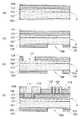
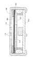
図1には本発明の音響検出機構の一例としてのシリコンコンデンサマイクホンの平面図を示し、図2には図1においてI−I線で切断された断面図を示している。このコンデンサマイクロホンは、〈1 0 0〉面方位である単結晶シリコン基板Aと一体的に振動板Bを形成し、この振動板Bと対向する位置に背電極Cを配置して小型のコンデンサを形成したものである。前記振動板BはSOI(Silicon on Insulator)ウエハーの活性層を用い、背電極Cはめっき技術によってアコースティクホールに相当する貫通穴Caを多数形成した平坦な(振動板Bと平行で均一の厚さとなる)金属膜を用い、振動板Bと背電極Cとの電極間距離を決めるスペーサDに低誘電率である感光性有機膜(犠牲層)を用いている。
【0028】
コンデンサマイクロホンの基板Aの大きさは平面視で縦横(Y/X)の寸法が5.5mmの正方形で厚さ(Z)は625μmである。図2では厚さを誇張して描いているが、振動板Bの厚さは5μmで大きさは平面視で縦横(y/x)の寸法が2mmの正方形である。背電極Cの厚さは10μmで一辺が20μm程度の正方形の前記貫通穴Caが複数個形成されている。この振動板Bならびに背電極Cの表面には信号取出し用の電極パッドE、Eが形成されている。前記貫通穴Caは平面視において中央位置に小さい開口となるものを配置し、中心から離間した位置に大きい開口となるものと配置している。このように貫通穴Caを形成することにより、背電極Cの側からの音響信号を振動板Bへ良好に伝えると同時に、この音響信号に基づく振動板Bの軽快な振動を実現するものとなっている。
【0029】
尚、前記基板Aに対してコンデンサマイクロホンの静電容量変化を電気信号に変換する変換回路や、この電気信号を増幅する増幅回路等を形成することも可能であり、このように回路を形成した場合には前記電極パッドE、Eと、これらの回路とがボンディングワイヤ等で結線される。
【0030】
図3(a)、(b)、(c)、(d)及び図4(e)、(f)、(g)に本発明のコンデンサマイクロホンの製造工程図を示している。この製造工程図では、(a)支持基板101と活性層102とを有した単結晶シリコン基板(活性層10μm/Box層1μm/支持基板600μm:以下、SOI基板と称する)の両面に対して絶縁膜103を形成する工程。表面に犠牲層104を形成する工程。(b・c)このSOI基板に保護層105を形成した後、振動板Bに対応した開口部106と、振動板Bから導通取出し用のコンタクトホール107とを設ける工程。(d)シード層108とレジストパターン109とを形成した後、めっき技術によって背電極110(C)を形成する工程。(e・f)レジストパターン109を取り除いた後、異方性エッチングにより振動板を形成する工程。(g)犠牲層104を除去する空隙領域形成工程を順次行うよう設定され、この工程の後に電極パッドEを形成するよう順序が設定され、以下、この製造工程の詳細を説明する。
【0031】
(a):支持基板101と活性層102とを有したSOI基板Aの表裏両面に対して熱酸化により酸化膜(SiO2膜)を作り出して絶縁膜103を形成し、表面側に犠牲層104を5μmの厚さとなるよう塗布により形成する。この犠牲層104は低誘電率の有機膜であるSU−8(誘電率3.0/エポキシ系レジスト)を用いている。このSU−8を用いることによって犠牲層の材料の一例としてのSiO2膜(誘電率3.8)を用いたもの比較すると、本SU−8は低誘電率であるのでマイクロホンの寄生容量の低減を可能にしている。尚、本発明は、犠牲層104としてSiO2膜を形成することを除外するものでは無い。
【0032】
また、前記活性層101の厚みは1〜10μmの範囲で調節することが可能であり、振動板Bとして形成した状態における感度や耐久性等を考慮して5μmに厚さが設定され、前記有機膜SU−8を用いた場合には粘度によって所望のスペーサ厚さとして層厚を2〜10μmに設定することができる。
【0033】
(b):次に、裏面側に振動板を形成する際のマスク材料としてSiNで成る保護膜105を成膜する。この保護膜105はフォトリソグラフィ技術を用いて形成され、レジストパターンとして機能するものであり、この保護層105において振動板を形成する部位に開口106が形成される。この後(f)で説明するように、このレジストパターンをマスクにしてRIE(Reactive Ion Etching)を用いてエッチングする加工により支持基板101部分が除去されて開口部111が形成される。
【0034】
(c):次に、表面側から活性層102、即ち、振動板領域に導通する部位を露出させるためのコンタクトホール107を設ける。つまり、同図には示していないが、従来からのフォトリソグラフィ技術を用いて形成されたレジストパターンをマスクにしてRIE(Reactive Ion Etching)を用いて犠牲層104と絶縁膜103とをエッチングする加工よりコンタクトホール107を形成する。
【0035】
(d):次に、表面側にスパッタの技術により、犠牲層104の表面、コンタクトホール107の部位の全ての表面にシード層108をスパッタリングにより形成し、更に、フレーム形成用のレジストパターン109(モールド)を形成した後に、めっきによって背電極110を形成する。このめっきは、金属材料としてNiを用い、応力が緩和される条件にて無電解めっきにより形成する。
【0036】
(e):次に、不要となっためっきフレーム形成用レジストパターン109を除去し、シード層108を除去することで、複数の貫通穴Caを有した背電極Cが現れる。
【0037】
(f):次に、ウエハー表面側即ち背電極側に保護膜を形成後、裏面からTMAH(テトラメチルアンモニウムハイドロオキサイド)の水溶液にて異方性エッチングを行い、活性層102(振動板B)の部位まで開放する開口部111を形成する。この後、不要となった保護膜105と酸化膜103とを除去する。
【0038】
(g):最後に犠牲層104をアッシングにより振動板と背電極との電極間距離を決めるスペーサ以外の領域を除去して空隙領域を形成し、電極パッドE(図1、図2を参照)を形成してマイクロホンが完成する。尚、犠牲層104がSiO2膜で形成されている場合には、この犠牲層104を除去する際にBHF(Buffered Hydrofluoric acid)によるエッチングを行うことになる。
【0039】
このような製造工程によって図1、図2に示すマイクロホンが製造される。このマイクロホンは、基板Aと一体的に振動板Bを形成し、かつ、この基板Aの表面側においてスペーサDを挟み込む位置に背電極Cを重畳配置し、この背電極Cがアコースティックホールに相当する多数の貫通穴Caを有した構造のものをめっきの技術によって形成したものとなっている。このように製造されたコンデンサマイクロホンは極めて小型にできることから携帯電話機のような小型の機器に対して容易に用いることが可能となるばかりか、プリント基板上に実装する場合にも、高温でのリフロー処理にも耐え得るのでマイクロホンを有した装置の組立を容易にするものになっている。
【0040】
また、このコンデンサマイクロホンでは、〈1 0 0〉面方位のシリコン基板特有の性質を利用して選択的にエッチングを行うことによりエッチングパターンに従い基板Aと一体的に精密加工された状態で振動板Bを形成できるものにしており、しかも、低誘電率の有機膜で成る犠牲層104を塗布により形成するので、この犠牲層104を簡単な処理によって任意の厚さに形成できるばかりでなく、この犠牲層104をスペーサとして機能させるので振動板Bと背電極Cとの間隔を比較的大きく設定して寄生容量の低減を可能にしている。また、めっきにより背電極Cを形成するので簡単な処理で比較的厚い金属膜として該背電極Cを形成できるばかりでなく、応力が作用しない状態で形成するので、この背電極Cに変形や歪みを発生させないものにして、高感度のマイクロホンとして機能する。
【0041】
〔別実施の形態〕
本発明は上記実施の形態以外に、例えば、以下のように構成して実施することも可能である。
【0042】
(イ)SOI基板を用いたが、これに代えて〈1 0 0〉面方位であるシリコン基板Aを用い、最終的に振動板Bが形成される側から(不純物拡散により)不純物を注入して異方性エッチング時にエッチングが進まないエッチストップ層を形成することで異方性エッチング後に所望の振動板Bを作製する。このように構成することで、前述した実施の形態と同様にエッチング処理によりエッチングパターンに基づき精密加工によって振動板Bを形成することが可能となる。
【0043】
(ロ)図5及び図6に示すように、背電極Cの形状を設定する。これらの図面に示すように背電極Cの形状は必ずしも矩形に形成する必要は無く、図6に示すように十字形状に形成することも可能である(この別実施の形態では前記実施の形態と同じ機能を有するものには、実施の形態と共通の番号、符号を付している)。尚、このような形状に背電極Cを形成した場合には、振動板Bは背電極Cの形状と等しいものが良いが、背電極Cと異なる形状に形成してもコンデンサマイクロホンとしての機能を損なうものではない。
【0044】
(ハ)本発明の構成を用いて音圧を検出するセンサを構成する。又、本発明の音響検出機構は基板の形状が正方形である必要は無く、矩形や多角形に形成することも可能である。特に、エッチングパターンの形状の設定により振動板の形状は円形や多角形に形成することも容易に行えるものであり、このように形状を設定することで、必要とする性能を現出することが可能となる。
【図面の簡単な説明】
【図1】コンデンサマイクロホンの平面図
【図2】コンデンサマイクロホンの断面図
【図3】コンデンサマイクロホンの製造プロセスを連続的に示す断面図
【図4】コンデンサマイクロホンの製造プロセスを連続的に示す断面図
【図5】別実施の形態の背電極の形状を示す平面図
【図6】別実施の形態の背電極の形状を示す平面図
【図7】従来のコンデンサマイクロホンの構造を示す断面図
【符号の説明】
104 犠牲層
A 基板
B 振動板
C 背電極
Ca 貫通穴
D スペーサ[0001]
TECHNICAL FIELD OF THE INVENTION
The present invention has a pair of electrodes forming a capacitor on a single crystal silicon substrate, and one of the pair of electrodes is a back electrode having at least one through hole corresponding to an acoustic hole, and the other is a back electrode. The electrodes are related to an acoustic detection mechanism that is a diaphragm, and more particularly, to an acoustic detection mechanism represented by a sensor for measuring an acoustic signal and a microphone.
[0002]
[Prior art]
Conventionally, as similar to the acoustic detection mechanism configured as described above, a vibration plate is formed integrally with a support substrate, and a back plate is formed on the support substrate via a gap layer formed by a support portion. There is a pressure sensor arranged (for example, Patent Document 1), and there is a pressure sensor configured as a condenser microphone having a structure in which a diaphragm and electrodes are formed on a substrate such as a silicon wafer (for example, Patent Document 2).
[0003]
[Patent Document 1]
JP-A-2002-27595 (Claims 4 to 5, paragraph numbers [0030] to [0040], FIGS. 1, 3 to 6)
[Patent Document 2]
JP-A-2002-209298 (Claims 1, Claims 2, Claims 11, Claims 12, paragraph numbers [0024] to [0095], FIGS. 1 to 10)
[0004]
[Problems to be solved by the invention]
In addition to the condenser microphones described in Patent Literature 1 and Patent Literature 2, the structure of an electret condenser microphone that has been frequently used in portable telephones can be shown in FIG. The condenser microphone includes a
[0005]
The electret condenser microphone shown in the figure applies an
[0006]
In this type of condenser microphone, it is necessary to increase the capacitance value in order to increase the output. To increase the capacitance value, the overlapping area between the fixed electrode layer and the
[0007]
In particular, in the case of an electret condenser microphone, an organic polymer such as FEP (Fluoro Ethylene Propylene) is used as an electret element which is a dielectric substance having permanent electric polarization applied to elements such as a condenser microphone. However, there is a problem that it is difficult to use as a reflow element when mounted on a substrate due to poor heat resistance.
[0008]
Therefore, by adopting the technology described in Patent Document 1 (Japanese Patent Application Laid-Open No. 2002-27595), the above-described conventional disadvantages are eliminated, the moisture resistance is excellent, and the device can be used as a reflow element. It is conceivable to construct a possible condenser microphone. In the condenser microphone of Patent Document 1, the distance between the fixed electrode layer and the diaphragm is reduced by silicon micromachining technology, that is, processing of a silicon substrate using a semiconductor processing technology, and fixed by the silicon micromachining technology. The interval between the electrode layer and the diaphragm can be set to an arbitrary interval. In addition, the condenser microphone of Patent Document 1 requires a bias power supply. However, since the electret element is not used and the silicon substrate itself is an electrode layer, the heat resistance is increased as compared with the electret condenser microphone, and the substrate mounting process in a later process is performed. Thus, it is considered that the problem of the temperature rise can be solved.
[0009]
In the condenser microphone disclosed in Patent Document 1, the diaphragm and the back electrode are combined by using a CVD (Chemical Vapor Depositoin) technique or the like via an adhesive layer containing boric acid or phosphorus containing silicon oxide in a high concentration at a high concentration. Thereafter, heat treatment is performed for bonding, and after this bonding, processing is performed by polishing to a desired back electrode thickness, an acoustic hole is formed on the back electrode side, and a diaphragm is formed by anisotropic etching from the back surface of the substrate. Finally, the void region and the support portion are formed by hydrofluoric acid.
[0010]
In this method, in addition to the problem of the reliability of the distance between the diaphragm and the back electrode in the bonding process, there is a problem that the parasitic capacitance due to the spacer that determines the distance between the diaphragm and the back electrode lowers the sensitivity. In other words, the dielectric constant of the spacer used in the present invention is very large, that is, 4 to 4.5, and the parasitic capacitance becomes large, which significantly affects the sensitivity. As another measure for reducing the parasitic capacitance of the above-described problem, in another embodiment of Patent Document 1, a substrate is etched so that a region corresponding to a diaphragm becomes convex, and a step is formed. There is a description that parasitic capacitance can be reduced by forming a support portion having a larger gap than the counter electrode gap by flattening by a technique such as polishing after forming an adhesive layer for use. However, in this embodiment, although effective in reducing the parasitic capacitance, the steps are complicated and the production efficiency is low, and the flatness accuracy by the technique such as polishing and the difficulty in obtaining a uniform adhesive layer thickness are great. Will be an issue.
[0011]
It is also conceivable to adopt the configuration described in Patent Document 2 (Japanese Patent Application Laid-Open No. 2002-209298) for the purpose of solving the above-mentioned inconvenience. However, in this configuration, the spacer itself is formed by the back electrode portion and is bonded to the semiconductor substrate with the insulating film interposed therebetween. Since the thickness of the insulating film itself is 1 μm or less, parasitic capacitance occurs in the bonded region. There is a problem that the sensitivity is easily lowered.
[0012]
SUMMARY OF THE INVENTION An object of the present invention is to solve the above-mentioned conventional disadvantages and to provide an acoustic detection mechanism capable of reducing a parasitic capacitance by a process in which a diaphragm and a back electrode can be manufactured on the same substrate without performing a bonding process. .
[0013]
[Means for Solving the Problems]
The features, functions and effects of the sound detection mechanism according to claim 1 of the present invention are as follows.
〔Characteristic〕
A single-crystal silicon substrate has a pair of electrodes forming a capacitor, one of the pair of electrodes is a back electrode having at least one through hole corresponding to an acoustic hole, and the other is a vibrating electrode. In the acoustic detection mechanism that is a plate, the diaphragm is formed of single-crystal silicon, and the back electrode is formed of a metal film formed by a plating technique, and an inter-electrode distance between the diaphragm and the back electrode. Is characterized in that the spacer for determining the above is composed of a part of the sacrificial layer.
[0014]
[Action / Effect]
According to the above feature, since the diaphragm can be formed by single crystal silicon, it is not necessary to form a special film or layer on the surface of the single crystal silicon to form the diaphragm. In addition, since the back electrode is formed of a metal film by a plating technique, the back electrode is formed to a required thickness in a short time using a good conductor by a simple process using a conventional semiconductor processing technique. It becomes possible. In addition, the spacer between the diaphragm and the back electrode is formed by a part of the sacrificial layer, so that a spacer having a required thickness can be formed, and between the diaphragm and the back electrode by etching or ashing. The diaphragm and the back electrode can be maintained in an insulated state by a part of the sacrificial layer while a gap can be easily formed. As a result, not only can it be easily manufactured by simple processing using conventional semiconductor processing technology, but also a spacer (sacrificial layer) having a low dielectric constant can be used, and the thickness of the spacer (sacrificial layer) can be reduced. An acoustic detection mechanism that can be thinned to reduce parasitic capacitance has been constructed.
[0015]
The features, functions and effects of the sound detection mechanism according to claim 2 of the present invention are as follows.
〔Characteristic〕
2. The acoustic detection mechanism according to claim 1, wherein the sacrificial layer is formed of a SiO2 film or an organic film.
[0016]
[Action / Effect]
According to the above features, it is possible to use a SiO2 film that can be formed by a simple process using a conventional semiconductor processing technique, or to use an organic film that can keep the dielectric constant low. As a result, an acoustic detection mechanism capable of exhibiting the required performance was constructed.
[0017]
The features, functions and effects of the sound detection mechanism according to claim 3 of the present invention are as follows.
〔Characteristic〕
2. The sound detection mechanism according to claim 1, wherein the back electrode has a flat structure.
[0018]
[Action / Effect]
According to the above feature, by making the back electrode flat, it is possible to eliminate bias of the capacitance with respect to each part of the surface of the diaphragm. As a result, an acoustic detection mechanism with uniform performance and high acoustic performance was constructed.
[0019]
The features, functions and effects of the sound detection mechanism according to claim 4 of the present invention are as follows.
〔Characteristic〕
2. The acoustic detection mechanism according to claim 1, wherein the sacrificial layer is formed of a material having a low dielectric constant.
[0020]
[Action / Effect]
According to the above feature, it is possible to positively reduce the parasitic capacitance at the portion where the capacitor is formed. As a result, a highly sensitive sound detection mechanism was constructed.
[0021]
The features, functions and effects of the sound detection mechanism according to claim 5 of the present invention are as follows.
〔Characteristic〕
2. The acoustic detection mechanism according to claim 1, wherein an SOI wafer having an active layer is used as the substrate, and the diaphragm is formed on the active layer, and the thickness of the active layer is 1 to 10 μm. It is a feature.
[0022]
[Action / Effect]
According to the above feature, not only can the diaphragm integrated with the substrate be formed by performing etching that leaves the active layer in the SOI wafer, but the thickness of the diaphragm can be set to an arbitrary thickness of 1 to 10 μm. It becomes possible to set it. As a result, an acoustic detection mechanism capable of easily forming a diaphragm having an arbitrary thickness of 1 to 10 μm as required was constructed.
[0023]
The features, functions and effects of the sound detection mechanism according to claim 6 of the present invention are as follows.
〔Characteristic〕
2. The acoustic detection mechanism according to claim 1, wherein the substrate is a silicon substrate having a <100> plane orientation.
[0024]
[Action / Effect]
According to the above feature, the etching can be selectively advanced in the direction of the <100> plane orientation peculiar to the silicon substrate, so that fine etching faithful to the etching pattern can be performed. As a result, an acoustic detection mechanism having a diaphragm having a required shape was formed by precision machining.
[0025]
The features, functions and effects of the sound detection mechanism according to claim 7 of the present invention are as follows.
〔Characteristic〕
The acoustic detection mechanism according to claim 5, wherein the active layer forming the diaphragm is diffused with impurities.
[0026]
[Action / Effect]
According to the above-described feature, by diffusing impurities into the active layer, the active layer can be set to a desired thickness as an etch stop layer where etching does not proceed during anisotropic etching. As a result, an acoustic detection mechanism having a diaphragm having a desired thickness was configured.
[0027]
BEST MODE FOR CARRYING OUT THE INVENTION
Hereinafter, embodiments of the present invention will be described with reference to the drawings.
FIG. 1 is a plan view of a silicon condenser microphone as an example of the sound detection mechanism of the present invention, and FIG. 2 is a cross-sectional view taken along line II in FIG. In this condenser microphone, a diaphragm B is formed integrally with a single-crystal silicon substrate A having a <100> plane orientation, and a back electrode C is arranged at a position facing the diaphragm B to provide a small capacitor. It was formed. The diaphragm B uses an active layer of an SOI (Silicon on Insulator) wafer, and the back electrode C has a flat (parallel and uniform thickness with the diaphragm B) in which a large number of through holes Ca corresponding to acoustic holes are formed by a plating technique. A photosensitive organic film (sacrifice layer) having a low dielectric constant is used for the spacer D that determines the inter-electrode distance between the diaphragm B and the back electrode C.
[0028]
The size of the substrate A of the condenser microphone is 5.5 mm square in vertical and horizontal (Y / X) dimensions in plan view, and the thickness (Z) is 625 μm. Although the thickness is exaggerated in FIG. 2, the thickness of the diaphragm B is 5 μm, and the size thereof is a square having a size of 2 mm in length and width (y / x) in plan view. The back electrode C has a thickness of 10 μm and a plurality of square through holes Ca each having a side of about 20 μm. On the surfaces of the diaphragm B and the back electrode C, electrode pads E, E for taking out signals are formed. The through hole Ca has a small opening at the center position in plan view, and has a large opening at a position away from the center. By forming the through-holes Ca in this manner, an acoustic signal from the back electrode C side is transmitted well to the diaphragm B, and at the same time, light vibration of the diaphragm B based on the acoustic signal is realized. ing.
[0029]
Note that it is also possible to form a conversion circuit for converting a change in capacitance of the condenser microphone into an electric signal, an amplifier circuit for amplifying the electric signal, and the like on the substrate A, and the circuit is formed in this manner. In this case, the electrode pads E, E and these circuits are connected by bonding wires or the like.
[0030]
3 (a), 3 (b), 3 (c), 3 (d) and 4 (e), 4 (f), 4 (g) show manufacturing process diagrams of the condenser microphone of the present invention. In this manufacturing process diagram, (a) both sides of a single-crystal silicon substrate having a
[0031]
(A): An oxide film (SiO 2 film) is formed by thermal oxidation on both front and back surfaces of an SOI substrate A having a
[0032]
The thickness of the
[0033]
(B): Next, a
[0034]
(C): Next, a
[0035]
(D): Next, the
[0036]
(E): Next, by removing the unnecessary plating frame forming resist
[0037]
(F): Next, after forming a protective film on the front surface side of the wafer, that is, on the back electrode side, anisotropic etching is performed from the back surface with an aqueous solution of TMAH (tetramethylammonium hydroxide) to form the active layer 102 (diaphragm B). An
[0038]
(G): Finally, the
[0039]
The microphone shown in FIGS. 1 and 2 is manufactured by such a manufacturing process. In this microphone, a diaphragm B is formed integrally with a substrate A, and a back electrode C is superposed and arranged at a position sandwiching a spacer D on the front side of the substrate A, and the back electrode C corresponds to an acoustic hole. A structure having a large number of through holes Ca is formed by plating technology. Since the condenser microphone manufactured in this way can be made extremely small, it can be easily used for a small device such as a mobile phone, and even when mounted on a printed circuit board, reflow at a high temperature. Since it can withstand processing, it is easy to assemble a device having a microphone.
[0040]
Further, in this condenser microphone, the diaphragm B is processed in a state where it is precision-processed integrally with the substrate A in accordance with the etching pattern by selectively performing etching by using the characteristic property of the silicon substrate having the <100> plane orientation. Is formed, and the
[0041]
[Another embodiment]
The present invention can be implemented with, for example, the following configuration in addition to the above embodiment.
[0042]
(A) Although an SOI substrate was used, a silicon substrate A having a <100> plane orientation was used instead, and an impurity was implanted (by impurity diffusion) from the side where the diaphragm B was finally formed. Thus, a desired diaphragm B is formed after the anisotropic etching by forming an etch stop layer which does not progress during the anisotropic etching. With this configuration, the diaphragm B can be formed by precision processing based on the etching pattern by the etching process as in the above-described embodiment.
[0043]
(B) As shown in FIGS. 5 and 6, the shape of the back electrode C is set. As shown in these drawings, the shape of the back electrode C does not necessarily need to be formed in a rectangular shape, and may be formed in a cross shape as shown in FIG. 6 (this alternative embodiment differs from the above-described embodiment. Those having the same functions are denoted by the same reference numerals and symbols as in the embodiment. When the back electrode C is formed in such a shape, the diaphragm B preferably has the same shape as the back electrode C. However, even if the diaphragm B is formed in a shape different from the back electrode C, the function as a condenser microphone is obtained. It doesn't hurt.
[0044]
(C) A sensor for detecting sound pressure is configured using the configuration of the present invention. In addition, the sound detection mechanism of the present invention does not need to have a square substrate, but can be formed in a rectangular or polygonal shape. In particular, by setting the shape of the etching pattern, the shape of the diaphragm can easily be formed into a circle or a polygon, and by setting the shape in this way, the required performance can be exhibited. It becomes possible.
[Brief description of the drawings]
FIG. 1 is a plan view of a condenser microphone. FIG. 2 is a cross-sectional view of a condenser microphone. FIG. 3 is a cross-sectional view continuously showing a manufacturing process of a condenser microphone. FIG. 4 is a cross-sectional view continuously showing a manufacturing process of a condenser microphone. FIG. 5 is a plan view showing the shape of a back electrode according to another embodiment. FIG. 6 is a plan view showing the shape of a back electrode according to another embodiment. FIG. 7 is a cross-sectional view showing the structure of a conventional condenser microphone. Description]
104 sacrificial layer A substrate B diaphragm C back electrode Ca through hole D spacer
Claims (7)
Translated fromJapanese前記振動板が単結晶シリコンにて形成されると共に、前記背電極がめっき技術にて形成される金属膜で成り、前記振動板と前記背電極との電極間距離を決めるスペーサが犠牲層の一部から成ることを特徴とする音響検出機構。A single-crystal silicon substrate has a pair of electrodes forming a capacitor, one of the pair of electrodes is a back electrode having at least one through hole corresponding to an acoustic hole, and the other is a vibrating electrode. In the sound detection mechanism that is a plate,
The vibrating plate is formed of single crystal silicon, the back electrode is formed of a metal film formed by a plating technique, and a spacer for determining an inter-electrode distance between the vibrating plate and the back electrode is one of the sacrificial layers. An acoustic detection mechanism comprising:
Priority Applications (1)
| Application Number | Priority Date | Filing Date | Title |
|---|---|---|---|
| JP2002256669AJP2004096543A (en) | 2002-09-02 | 2002-09-02 | Sound detection mechanism |
Applications Claiming Priority (1)
| Application Number | Priority Date | Filing Date | Title |
|---|---|---|---|
| JP2002256669AJP2004096543A (en) | 2002-09-02 | 2002-09-02 | Sound detection mechanism |
Publications (1)
| Publication Number | Publication Date |
|---|---|
| JP2004096543Atrue JP2004096543A (en) | 2004-03-25 |
Family
ID=32061834
Family Applications (1)
| Application Number | Title | Priority Date | Filing Date |
|---|---|---|---|
| JP2002256669APendingJP2004096543A (en) | 2002-09-02 | 2002-09-02 | Sound detection mechanism |
Country Status (1)
| Country | Link |
|---|---|
| JP (1) | JP2004096543A (en) |
Cited By (3)
| Publication number | Priority date | Publication date | Assignee | Title |
|---|---|---|---|---|
| WO2005079112A1 (en)* | 2004-02-13 | 2005-08-25 | Tokyo Electron Limited | Capacity detection type sensor element |
| WO2008149571A1 (en)* | 2007-06-04 | 2008-12-11 | Omron Corporation | Acoustic sensor |
| WO2008149570A1 (en)* | 2007-06-04 | 2008-12-11 | Omron Corporation | Acoustic sensor |
- 2002
- 2002-09-02JPJP2002256669Apatent/JP2004096543A/enactivePending
Cited By (5)
| Publication number | Priority date | Publication date | Assignee | Title |
|---|---|---|---|---|
| WO2005079112A1 (en)* | 2004-02-13 | 2005-08-25 | Tokyo Electron Limited | Capacity detection type sensor element |
| WO2008149571A1 (en)* | 2007-06-04 | 2008-12-11 | Omron Corporation | Acoustic sensor |
| WO2008149570A1 (en)* | 2007-06-04 | 2008-12-11 | Omron Corporation | Acoustic sensor |
| US8379887B2 (en) | 2007-06-04 | 2013-02-19 | Omron Corporation | Acoustic sensor |
| US8699728B2 (en) | 2007-06-04 | 2014-04-15 | Omron Corporation | Acoustic sensor |
Similar Documents
| Publication | Publication Date | Title |
|---|---|---|
| US7386136B2 (en) | Sound detecting mechanism | |
| US4558184A (en) | Integrated capacitive transducer | |
| JP3451593B2 (en) | Solid state condenser and microphone device | |
| KR101807146B1 (en) | High sensitivity microphone and manufacturing method thereof | |
| CN108124226B (en) | Integrated electro-acoustic MEMS transducer with improved sensitivity and manufacturing process thereof | |
| KR20060033021A (en) | Acoustic detection equipment | |
| KR100716637B1 (en) | Acoustic Detection Mechanism and Manufacturing Method Thereof | |
| US20230234837A1 (en) | Mems microphone with an anchor | |
| US20230239641A1 (en) | Method of making mems microphone with an anchor | |
| CN105704629B (en) | Microphone and the method for manufacturing the microphone | |
| JP2011250170A (en) | Acoustic sensor, acoustic transducer and microphone using acoustic transducer, and method for producing acoustic transducer | |
| CN103139691A (en) | Micro-electromechanical system (MEMS) silicon microphone utilizing multi-hole signal operation instruction (SOI) silicon bonding and manufacturing method thereof | |
| CN204836579U (en) | Comb tooth structure MEMS silicon microphone | |
| JP2004128957A (en) | Sound detection mechanism | |
| JP2010506532A (en) | Extremely low pressure sensor and method for manufacturing the same | |
| JP4737535B2 (en) | Condenser microphone | |
| JP4811035B2 (en) | Acoustic sensor | |
| JP2008252847A (en) | Electrostatic transducer | |
| US20210139319A1 (en) | Membrane Support for Dual Backplate Transducers | |
| JP2003163998A (en) | Method for manufacturing condenser microphone, condenser microphone, and electronic device | |
| JP2004096543A (en) | Sound detection mechanism | |
| KR100765149B1 (en) | Ultra-small acoustic sensing device and manufacturing method thereof | |
| CN114390418A (en) | MEMS electrode formation method | |
| JP2007329559A (en) | Condenser microphone and manufacturing method therefor | |
| KR101108853B1 (en) | Microphone module |
Legal Events
| Date | Code | Title | Description |
|---|---|---|---|
| A711 | Notification of change in applicant | Free format text:JAPANESE INTERMEDIATE CODE: A711 Effective date:20040203 | |
| A521 | Written amendment | Free format text:JAPANESE INTERMEDIATE CODE: A821 Effective date:20040203 | |
| A621 | Written request for application examination | Free format text:JAPANESE INTERMEDIATE CODE: A621 Effective date:20040702 | |
| A977 | Report on retrieval | Free format text:JAPANESE INTERMEDIATE CODE: A971007 Effective date:20060127 | |
| A131 | Notification of reasons for refusal | Free format text:JAPANESE INTERMEDIATE CODE: A131 Effective date:20060803 | |
| A521 | Written amendment | Free format text:JAPANESE INTERMEDIATE CODE: A523 Effective date:20061002 | |
| A131 | Notification of reasons for refusal | Free format text:JAPANESE INTERMEDIATE CODE: A131 Effective date:20071018 | |
| A02 | Decision of refusal | Free format text:JAPANESE INTERMEDIATE CODE: A02 Effective date:20080904 |