JP2004080033A - Fine pattern forming method using silicon oxide film - Google Patents
Fine pattern forming method using silicon oxide filmDownload PDFInfo
- Publication number
- JP2004080033A JP2004080033AJP2003290758AJP2003290758AJP2004080033AJP 2004080033 AJP2004080033 AJP 2004080033AJP 2003290758 AJP2003290758 AJP 2003290758AJP 2003290758 AJP2003290758 AJP 2003290758AJP 2004080033 AJP2004080033 AJP 2004080033A
- Authority
- JP
- Japan
- Prior art keywords
- pattern
- film
- silicon oxide
- oxide film
- photoresist
- Prior art date
- Legal status (The legal status is an assumption and is not a legal conclusion. Google has not performed a legal analysis and makes no representation as to the accuracy of the status listed.)
- Pending
Links
Images


Classifications
- H—ELECTRICITY
- H01—ELECTRIC ELEMENTS
- H01L—SEMICONDUCTOR DEVICES NOT COVERED BY CLASS H10
- H01L21/00—Processes or apparatus adapted for the manufacture or treatment of semiconductor or solid state devices or of parts thereof
- H01L21/02—Manufacture or treatment of semiconductor devices or of parts thereof
- H01L21/027—Making masks on semiconductor bodies for further photolithographic processing not provided for in group H01L21/18 or H01L21/34
- H—ELECTRICITY
- H01—ELECTRIC ELEMENTS
- H01L—SEMICONDUCTOR DEVICES NOT COVERED BY CLASS H10
- H01L21/00—Processes or apparatus adapted for the manufacture or treatment of semiconductor or solid state devices or of parts thereof
- H01L21/02—Manufacture or treatment of semiconductor devices or of parts thereof
- H01L21/04—Manufacture or treatment of semiconductor devices or of parts thereof the devices having potential barriers, e.g. a PN junction, depletion layer or carrier concentration layer
- H01L21/18—Manufacture or treatment of semiconductor devices or of parts thereof the devices having potential barriers, e.g. a PN junction, depletion layer or carrier concentration layer the devices having semiconductor bodies comprising elements of Group IV of the Periodic Table or AIIIBV compounds with or without impurities, e.g. doping materials
- H01L21/30—Treatment of semiconductor bodies using processes or apparatus not provided for in groups H01L21/20 - H01L21/26
- H01L21/31—Treatment of semiconductor bodies using processes or apparatus not provided for in groups H01L21/20 - H01L21/26 to form insulating layers thereon, e.g. for masking or by using photolithographic techniques; After treatment of these layers; Selection of materials for these layers
- H01L21/3205—Deposition of non-insulating-, e.g. conductive- or resistive-, layers on insulating layers; After-treatment of these layers
- H01L21/321—After treatment
- H01L21/3213—Physical or chemical etching of the layers, e.g. to produce a patterned layer from a pre-deposited extensive layer
- H01L21/32139—Physical or chemical etching of the layers, e.g. to produce a patterned layer from a pre-deposited extensive layer using masks
- G—PHYSICS
- G03—PHOTOGRAPHY; CINEMATOGRAPHY; ANALOGOUS TECHNIQUES USING WAVES OTHER THAN OPTICAL WAVES; ELECTROGRAPHY; HOLOGRAPHY
- G03F—PHOTOMECHANICAL PRODUCTION OF TEXTURED OR PATTERNED SURFACES, e.g. FOR PRINTING, FOR PROCESSING OF SEMICONDUCTOR DEVICES; MATERIALS THEREFOR; ORIGINALS THEREFOR; APPARATUS SPECIALLY ADAPTED THEREFOR
- G03F7/00—Photomechanical, e.g. photolithographic, production of textured or patterned surfaces, e.g. printing surfaces; Materials therefor, e.g. comprising photoresists; Apparatus specially adapted therefor
- G03F7/26—Processing photosensitive materials; Apparatus therefor
- G03F7/40—Treatment after imagewise removal, e.g. baking
- G03F7/405—Treatment with inorganic or organometallic reagents after imagewise removal
- H—ELECTRICITY
- H01—ELECTRIC ELEMENTS
- H01L—SEMICONDUCTOR DEVICES NOT COVERED BY CLASS H10
- H01L21/00—Processes or apparatus adapted for the manufacture or treatment of semiconductor or solid state devices or of parts thereof
- H01L21/02—Manufacture or treatment of semiconductor devices or of parts thereof
- H01L21/027—Making masks on semiconductor bodies for further photolithographic processing not provided for in group H01L21/18 or H01L21/34
- H01L21/0271—Making masks on semiconductor bodies for further photolithographic processing not provided for in group H01L21/18 or H01L21/34 comprising organic layers
- H01L21/0273—Making masks on semiconductor bodies for further photolithographic processing not provided for in group H01L21/18 or H01L21/34 comprising organic layers characterised by the treatment of photoresist layers
- H01L21/0274—Photolithographic processes
- G—PHYSICS
- G03—PHOTOGRAPHY; CINEMATOGRAPHY; ANALOGOUS TECHNIQUES USING WAVES OTHER THAN OPTICAL WAVES; ELECTROGRAPHY; HOLOGRAPHY
- G03F—PHOTOMECHANICAL PRODUCTION OF TEXTURED OR PATTERNED SURFACES, e.g. FOR PRINTING, FOR PROCESSING OF SEMICONDUCTOR DEVICES; MATERIALS THEREFOR; ORIGINALS THEREFOR; APPARATUS SPECIALLY ADAPTED THEREFOR
- G03F7/00—Photomechanical, e.g. photolithographic, production of textured or patterned surfaces, e.g. printing surfaces; Materials therefor, e.g. comprising photoresists; Apparatus specially adapted therefor
- G03F7/26—Processing photosensitive materials; Apparatus therefor
- G03F7/40—Treatment after imagewise removal, e.g. baking
Landscapes
- Engineering & Computer Science (AREA)
- Physics & Mathematics (AREA)
- General Physics & Mathematics (AREA)
- Condensed Matter Physics & Semiconductors (AREA)
- Manufacturing & Machinery (AREA)
- Computer Hardware Design (AREA)
- Microelectronics & Electronic Packaging (AREA)
- Power Engineering (AREA)
- Chemical & Material Sciences (AREA)
- Inorganic Chemistry (AREA)
- Organic Chemistry (AREA)
- Drying Of Semiconductors (AREA)
- Internal Circuitry In Semiconductor Integrated Circuit Devices (AREA)
- Semiconductor Memories (AREA)
- Exposure Of Semiconductors, Excluding Electron Or Ion Beam Exposure (AREA)
- Photosensitive Polymer And Photoresist Processing (AREA)
Abstract
Translated fromJapaneseDescription
Translated fromJapanese本発明は、半導体素子の微細パターン形成方法に係り、より具体的には、薄いシリコン酸化膜をフォトレジスト膜上に形成した後でドライエッチングすることによって微細パターンを形成する方法に関する。The present invention relates to a method for forming a fine pattern of a semiconductor device, and more specifically, to a method for forming a fine pattern by dry etching after forming a thin silicon oxide film on a photoresist film.
半導体装置の集積度が増加するにつれて、単位セルの面積もまた急速に狭まっている。単位セルの面積縮小は単位セルに具現される個別素子のサイズの縮小を伴う。トランジスタやキャパシタのサイズが小さくなるのと同時に配線の幅、配線と配線との間隔及び上下部素子を電気的に連結するコンタクトのサイズも微細化し続けている。(4) As the degree of integration of semiconductor devices increases, the area of unit cells also decreases rapidly. Reducing the area of a unit cell involves reducing the size of an individual device implemented in the unit cell. At the same time as the size of transistors and capacitors has been reduced, the width of wiring, the distance between wirings, and the size of contacts for electrically connecting upper and lower elements have also been miniaturized.
このように微細化した素子を製造するためには色々な工程条件が備えられなければならない。特に、微細化したパターンを精巧に製造できるためにはそれを裏付けられるフォトリソグラフィ技術が必須である。工程 Various process conditions must be provided to manufacture such miniaturized devices. In particular, in order to be able to precisely manufacture a fine pattern, a photolithography technique that can support the fine pattern is essential.
まず、素子の微細化でパターンのサイズが小さくなるので、臨界寸法(CD:critical dimension)の小さいフォトレジストパターンが必要である。そして、エッチング工程、特にドライエッチング工程中に微細なフォトレジストパターンに損傷が生じてはならない。{Circle over (1)] Since the size of the pattern becomes smaller due to the miniaturization of elements, a photoresist pattern having a small critical dimension (CD) is required. In addition, the fine photoresist pattern must not be damaged during the etching process, especially during the dry etching process.
フォトレジストパターンに生じる損傷には、パターンがの薄型化とパターンに生じる色々な変形が含まれる。パターンが薄くなればエッチングされる膜のパターンプロファイルが劣化され、フォトレジストに発生した変形によってエッチングされる下部膜にストリエーション及び/またはウィグリングなどが発生する問題が生じる。損傷 Damage to the photoresist pattern includes thinning of the pattern and various deformations to the pattern. As the pattern becomes thinner, the pattern profile of the film to be etched is degraded, and a problem arises that striation and / or wiggling occurs in the lower film to be etched due to deformation generated in the photoresist.
前記した問題点を解決するための方法では、多層レジスト(MLR:Multi―Layer Resist)を利用する方法(特許文献1参照)またはフォトレジストの表面にポリマーを生成させる方法(特許文献2参照)などが提示されている。しかし、前記した方法らはCDがごく小さくなるにつれて適用できなくなり、Si−CARL(Silicon−Chemical Amplication of resist Lines)工程を利用する場合には微細なパターン間に過度な不純物が発生して工程の負担を加重させる。
本発明が解決しようとする技術的課題は、微細化したフォトレジストパターンに損傷が生じることを防止することによって、パターンの薄型化、ストリエーション及び/またはウィグリングなどが発生せずに、一定のパターンプロファイルを有している高集積半導体素子の微細パターンを効率的に形成する方法を提供するところにある。The technical problem to be solved by the present invention is to prevent a fine photoresist pattern from being damaged, so that a thinned pattern, a striation and / or a wiggling can be prevented without causing a certain problem. It is an object of the present invention to provide a method for efficiently forming a fine pattern of a highly integrated semiconductor device having a pattern profile.
前記した技術的課題を達成するための本発明による微細パターン形成方法は、フォトレジストパターン上にシリコン酸化膜を薄く形成した後でドライエッチング工程を実施する。According to the method of forming a fine pattern according to the present invention, the dry etching process is performed after forming a thin silicon oxide film on a photoresist pattern.
本発明の望ましい実施例によれば、パターンを形成しようとする物質膜上にフォトレジスト膜を形成し、これを露光及び現像してフォトレジストパターンを形成する。次に、その上に前記したフォトレジストパターンに損傷が生じないようにコンフォーマルに(整合的に)第1シリコン酸化膜を薄く形成する。それから、前記した物質膜をドライエッチングすることによって物質膜パターンを形成する。According to a preferred embodiment of the present invention, a photoresist film is formed on a material film on which a pattern is to be formed, and the photoresist film is exposed and developed to form a photoresist pattern. Next, a first silicon oxide film is conformally (thinly) thinly formed thereon so as not to damage the photoresist pattern. Then, the material film is dry-etched to form a material film pattern.
フォトレジストパターンに損傷が生じないように第1シリコン酸化膜は常温〜400℃の間の温度で形成するのが望ましく、200Å以下の厚さに薄く形成するのが望ましい。このような第1シリコン酸化膜は原子層蒸着法(ALD)を利用して形成できる。The first silicon oxide film is preferably formed at a temperature between room temperature and 400 ° C. so as not to damage the photoresist pattern, and is preferably formed as thin as 200 ° or less. Such a first silicon oxide film may be formed using an atomic layer deposition (ALD) method.
形成された物質膜パターンはラインタイプパターンであることがあるが、この場合に前記した物質膜パターンはビットラインまたはワードラインのような導電ラインパターンでありうる。前記した導電ラインを形成するための物質膜は第2シリコン酸化膜、ポリシリコン膜、金属シリサイド膜及び反射防止膜の積層体でありうる。The formed material film pattern may be a line type pattern. In this case, the material film pattern may be a conductive line pattern such as a bit line or a word line. The material layer for forming the conductive line may be a stack of a second silicon oxide layer, a polysilicon layer, a metal silicide layer, and an anti-reflection layer.
そして、形成された物質膜パターンはホールタイプパターンでありうる。The formed material film pattern may be a hole type pattern.
本発明の望ましい他の実施例によれば、物質膜上にフォトレジスト膜を形成し、これを露光及び現像してフォトレジストパターンを形成する。次にその上に前記したフォトレジストパターンに損傷が生じないようにコンフォーマルに第1シリコン酸化膜を形成する。それから、前記した物質膜をドライエッチングするが、まずフォトレジストパターンより第1シリコン酸化膜に対してよりエッチングされ易い工程条件でエッチングした後、第1シリコン酸化膜よりフォトレジストパターンに対してよりエッチングされ易い工程条件でエッチングを実施して物質膜パターンを形成する段階を含む。According to another embodiment of the present invention, a photoresist film is formed on a material film, and the photoresist film is exposed and developed to form a photoresist pattern. Next, a first silicon oxide film is conformally formed thereon so as not to damage the photoresist pattern. Then, the material film is dry-etched. First, the first silicon oxide film is more easily etched than the photoresist pattern. Then, the first silicon oxide film is more etched than the photoresist pattern. Forming a material film pattern by performing etching under process conditions that are easily performed.
フォトレジストパターンに損傷が生じないように第1シリコン酸化膜は常温〜400℃の間の温度で形成するのが望ましく、200Å以下の厚さに薄く形成するのが望ましい。このような第1シリコン酸化膜はALDを利用して形成できる。The first silicon oxide film is preferably formed at a temperature between room temperature and 400 ° C. so as not to damage the photoresist pattern, and is preferably formed as thin as 200 ° or less. Such a first silicon oxide film can be formed using ALD.
前記した物質膜パターン形成段階で、第1シリコン酸化膜がよりエッチングされ易い工程条件ではフォトレジストパターンの側壁にシリコン酸化膜でスペーサを形成する段階を含むことができ、フォトレジストパターンがよりエッチングされやすい工程条件ではCxFyを含むポリマー膜がフォトレジストパターン上部に形成される段階を含むことができる。The step of forming the material film pattern may include forming a spacer with a silicon oxide film on a sidewall of the photoresist pattern under process conditions in which the first silicon oxide film is more easily etched, so that the photoresist pattern is more etched. in cheap process conditions may include the step of polymer film containing Cx Fy is formed in the photoresist pattern top.
このように形成された物質膜パターンはラインタイプパターンでありうるが、この場合に前記した物質膜パターンはビットラインまたはワードラインのような導電ラインパターンでありうる。前記した導電ラインを形成するための物質膜は第2シリコン酸化膜、ポリシリコン膜、金属シリサイド膜及び反射防止膜の積層体でありうる。The material layer pattern thus formed may be a line type pattern. In this case, the material layer pattern may be a conductive line pattern such as a bit line or a word line. The material layer for forming the conductive line may be a stack of a second silicon oxide layer, a polysilicon layer, a metal silicide layer, and an anti-reflection layer.
そして、形成された物質膜パターンはホールタイプパターンでありうる。The formed material film pattern may be a hole type pattern.
本発明による微細パターン形成方法によれば、フォトレジストパターンを形成した後でその上にシリコン酸化膜を形成することによって後続のドライエッチング工程中にフォトレジストパターンに損傷が生じることが防止できる。したがって、微細化したパターンを所望のプロファイルに形成でき、パターニングされた下部膜が薄くなったり、その下部膜にストリエーションやウィグリングが生じることが防止できる。そして、ホールタイプパターンの場合にはパターン間の間隔よりさらに小さいサイズのホールが形成できる。According to the method for forming a fine pattern according to the present invention, a photoresist pattern is formed and then a silicon oxide film is formed thereon, thereby preventing the photoresist pattern from being damaged during a subsequent dry etching process. Therefore, a miniaturized pattern can be formed in a desired profile, and the patterned lower film can be prevented from becoming thinner, and the lower film can be prevented from striation or wiggling. In the case of a hole type pattern, holes having a size smaller than the interval between the patterns can be formed.
以下、図面を参照して本発明の望ましい実施例を詳細に説明する。しかし、本発明はここで説明する実施例に限定されず、他の形態に具体化できる。むしろ、ここで紹介される実施例は本発明の技術的思想が徹底かつ完全に開示できるように、そして当業者に本発明の思想が十分に伝えられるようにするために提供されるものである。図面において、層領域の厚さは明確性を期するために誇張されている。また、ある層が他の層または基板“上”にあると言及した場合に、それは他の層または基板上に直接形成されたり、またはそれらの間に第3の層が介在されたことを意味する。明細書全体にかけて同じ参照番号は同じ構成要素を示す。Hereinafter, preferred embodiments of the present invention will be described in detail with reference to the drawings. However, the present invention is not limited to the embodiments described herein, but can be embodied in other forms. Rather, the embodiments described herein are provided so that the technical concept of the present invention may be disclosed in a thorough and complete manner and that the concept of the present invention may be sufficiently conveyed to those skilled in the art. . In the drawings, the thickness of layer regions is exaggerated for clarity. Also, when an element is referred to as being “on” another element or substrate, it means that it was formed directly on the other element or substrate, or that a third layer was interposed between them. I do. Like numbers refer to like elements throughout the specification.
図1Aないし図1Dは、本発明に実施例によって下部物質膜に微細パターンを形成する方法を示すために工程順序によって概略的に示す断面図である。FIGS. 1A to 1D are cross-sectional views schematically illustrating a method of forming a fine pattern on a lower material layer according to an embodiment of the present invention, according to a process sequence.
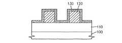
図1Aを参照すれば、基板100上に物質膜110が形成されている。この物質膜110は以後にエッチングされて所定のパターンが形成される膜である。物質膜110は特定の物質で形成された1つの膜である場合もあり、色々な他の物質で形成された膜が積み上げられている膜の積層体でありうる。例えば、物質膜110は絶縁物質よりなる膜であったり、導電物質よりなる膜である場合もあり、また単結晶シリコンのように半導体物質で形成された膜でありうる。また、絶縁物質よりなる膜及び/または導電物質よりなる膜が共に積層されている膜でありうる。図1Aないし図1Dには、物質膜が単一膜である場合を示しているが、図2Aないし図2Cにはいろいろな物質の膜が積層されている場合を示している。A Referring to FIG. 1A, a
次に、物質膜110上にフォトレジスト膜を所定の厚さに形成した後で、露光及び現象工程を実施する。それでは、図面でのように特定な形を有するフォトレジストパターン120が形成される。本実施例では、フォトレジスト膜に使われる物質には何の制限がない。そして、形成しようとするパターンの形にも何の制限がない。すなわち、前記したパターンはビットラインやワードラインのような導電ラインを形成するためのラインタイプのパターンである場合もあり、コンタクトを形成するためのホールタイプのパターンでもある。Next, after a photoresist film is formed on the
図1Bを参照すれば、物質膜110及びフォトレジストパターン120上にシリコン酸化膜130を蒸着する。本発明の技術的課題を達成するためにフォトレジストパターン120上にシリコン酸化膜130を蒸着するにおいて、次のような点を考慮せねばならない。1B, a
第1に、シリコン酸化膜130を蒸着する間にフォトレジストパターン120の構造や物性に変化が生じてはならない。すなわち、蒸着過程で化学物質やプラズマまたは熱によってフォトレジストパターン120に物理的、化学的損傷が生じてはならない。First, the structure and physical properties of the
第2に、シリコン酸化膜130が物質膜110上だけではなくフォトレジストパターン120上にもコンフォーマルに蒸着されねばならない。可能であれば、フォトレジストパターン120上にだけ形成するのがさらに望ましい。それとも、後続エッチング工程でシリコン酸化膜130の厚さによってエッチング率に差がつくので、エッチングプロファイルが悪くなる恐れがある。Second, the
第3に、蒸着されるシリコン酸化膜130の厚さを調節せねばならない。微細化したパターンの臨界寸法を考慮すれば、厚さをÅ単位に微細に調節可能でなければならない。Third, the thickness of the deposited
前記した条件を満足させる代表的な工程は、ALDがある。ALDは一般的に低温でも実施可能であり、ステップカバレッジ特性に優れてローディング効果もほとんど現れない。また、原子層を1層ずつ積み重ねる方法で蒸着されるので、厚さの微細調節が可能である。したがって、ALDを使用すれば、フォトレジストパターン120の損傷なしに所望の厚さのシリコン酸化膜をコンフォーマルに形成できる。しかし、本実施例はALDを使用したシリコン酸化膜の形成に限定されず、前記した条件を満足させるのであれば、いかなる工程にも適用可能である。A typical process that satisfies the above conditions is ALD. ALD can be generally performed even at a low temperature, has excellent step coverage characteristics, and hardly exhibits a loading effect. Further, since the atomic layers are deposited by stacking one layer at a time, the thickness can be finely adjusted. Therefore, if ALD is used, a silicon oxide film having a desired thickness can be formed conformally without damaging the
本実施例で、シリコン酸化膜130は常温〜400℃以下の温度で形成するのが望ましい。そして、シリコン酸化膜130は約200Å以下の厚さに形成するのが望ましいが、正確な厚さはフォトレジストパターン120間の間隔と形成しようとする物質膜パターンのプロファイルなどを考慮して決定する。で In this embodiment, it is desirable that the
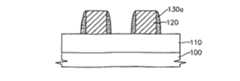
次に、前記した結果物に対してドライエッチング工程を実施して物質膜パターン110aを形成する。この過程が図1C及び図1Dに示されている。Next, a dry etching process is performed on the resultant to form a material film pattern 110a. This process is shown in FIGS. 1C and 1D.
図1Cを参照すれば、まず物質膜110のドライエッチング初期にフォトレジストパターン120の側壁にシリコン酸化膜よりなるスペーサ130aを形成する。このために工程初期には工程条件を調節してフォトレジストパターン120よりシリコン酸化膜130がよりエッチングされ易くする。スペーサ130aが形成される間に物質膜110も若干エッチングされうる。Referring to FIG. 1C, first, a
このように形成されたスペーサ130aはエッチングが進行される間に、フォトレジストパターン120の幅が薄くなることを防止する役割を果たす。スペーサ130aによってフォトレジストパターン120の側壁に原子やプラズマイオンが衝突することを防止できるからである。また、スペーサは、図1Dに示すようにフォトレジストパターン120の損傷で生じるポリマーがフォトレジストパターン120の上部に積層されることを助ける役割もする。(4) The
図1Dを参照すれば、エッチング工程を進行し続けて物質膜パターン110aを形成する。この時には従来とは違ってシリコン酸化膜130よりフォトレジストパターン120がよりエッチングされ易く工程条件を調節してエッチングを進められる。それでは、物質膜110をエッチングして物質膜パターン110aを形成する間にスペーサ130aに対するエッチング率は低くなって、フォトレジストパターン120aに対するエッチング率は高まり、フォトレジストパターン120aに損傷が生じる。Referring to FIG. 1D, the material layer pattern 110a is formed by continuing the etching process. At this time, unlike the conventional case, the
フォトレジストパターンに損傷が生じれば、フォトレジスト物質とエッチングガスとが反応して有機物質のポリマーを生成する。例えば、このようなポリマーは炭素とフッ素とを含む物質でありうる。ポリマーが生成されれば前述したようにフォトレジストパターン120の側壁にはスペーサ130aがあるので、フォトレジストパターン120の上部に積み上げられてポリマー膜121が形成される。ポリマー膜121はその下部に残っているフォトレジストパターン120aにこれ以上損傷が生じることを防止する役割を果たす。フォトレジストパターン120aにこれ以上損傷が生じないとエッチングされる物質膜パターン110aの薄型化、ストリエーション及びウィグリングなどが生じない。If the photoresist pattern is damaged, the photoresist material reacts with the etching gas to generate an organic polymer. For example, such a polymer can be a substance containing carbon and fluorine. If the polymer is generated, the
このように、ドライエッチング工程を進行し続けると、物質膜パターン110aが形成される。図面には物質膜パターン110aが全体物質膜に形成される場合を示しているが、本実施例は形成される物質膜パターン110aの深さには関係なく適用可能である。例えば、物質膜110が単一膜である場合にその全体深さまでエッチングされて物質膜パターン110aが形成される場合もあり、全体深さの一部だけエッチングされて物質膜パターンが形成される場合もある。物質膜110がいろいろな物質の膜が積層されている膜である場合にも積層体の全部または一部にパターンが形成されうる。(4) As the dry etching process proceeds, the material film pattern 110a is formed. Although the drawing shows a case where the material film pattern 110a is formed on the entire material film, the present embodiment can be applied regardless of the depth of the material film pattern 110a to be formed. For example, when the
そして、エッチング工程を進行し続ければ、シリコン酸化膜で薄く形成されたスペーサ130aがすべて除去されることもある。(4) If the etching process is continued, all the
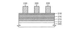
図2Aないし図2C及び図3は、本発明によってラインタイプのパターンを形成する過程及びそれに関する結果を走査電子顕微鏡(SEM)で撮影した写真を示している。図3の写真のうちから最初の写真は本実施例と比較するためのものであって、図2Aに示している状態で第1シリコン酸化膜230を形成せずにエッチング工程を実施した後のパターンプロファイルを示す写真である。そして、第2ないし第4の写真は、図2Bのように第1シリコン酸化膜230を形成した状態でエッチング工程を実施した後のパターンプロファイルを示す写真であって、第1シリコン酸化膜230をそれぞれ10Å、50Å及び100Åの厚さに形成した場合である。FIGS. 2A to 2C and FIG. 3 are photographs taken by a scanning electron microscope (SEM) of a process of forming a line-type pattern according to the present invention and results thereof. The first of the photographs in FIG. 3 is for comparison with the present embodiment, and after performing the etching process without forming the first
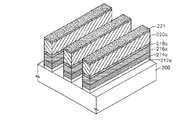
図2Aないし図2Cを参照すれば、基板200上に第2シリコン酸化膜212、ポリシリコン膜214、金属シリサイド膜216及びエッチング防止膜218の積層体が形成されている。この積層体は、例えばビットラインやワードラインのようにラインタイプのパターン形成に使われうる。2A to 2C, a stacked body of a second
本実施例で、第2シリコン酸化膜212は、約1200Å程度、ポリシリコン膜214は約1150Å程度、金属シリサイド膜216はタングステンシリサイド(WSi)を約1500Å程度、そして反射防止膜118は約240Å程度の厚さに蒸着した。そして、反射防止膜118上にフォトレジストパターン220を形成した後、反射防止膜118及びフォトレジストパターン220上に第1シリコン酸化膜230をALDを利用して形成し、ドライエッチング工程を実施した。In this embodiment, the second
図3のエッチング結果を述べれば、第1シリコン酸化膜230が厚くなるほどパターンのプロファイルが向上することが分かる。すなわち、第1シリコン酸化膜230を形成しない場合よりは形成した場合にパターンのプロファイルがさらに鮮明であり、第1シリコン酸化膜230を100Åに厚く形成した場合には所望のパターンのプロファイルとほとんど類似しているのが分かる。(3) Referring to the etching result of FIG. 3, it can be seen that the pattern profile improves as the first
しかし、所定の物質膜をエッチングして所望の形のパターンを形成するためにはパターンプロファイル結果だけでなく形成しようとするパターンのサイズ及び隣接したパターン間の間隔など色々な条件を考慮すべきである。パターンのサイズ及び隣接したパターン間の間隔によって蒸着できる第1シリコン酸化膜の厚さが制限されるので、エッチング工程を進行する前にこれを考慮すべきである。However, in order to form a pattern having a desired shape by etching a predetermined material film, not only a pattern profile result but also various conditions such as a size of a pattern to be formed and a space between adjacent patterns should be considered. is there. Since the thickness of the first silicon oxide film that can be deposited is limited by the size of the pattern and the distance between adjacent patterns, it is necessary to consider this before proceeding with the etching process.
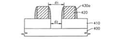
次に、図4を参照して本発明の実施例を適用可能な他の例について述べる。図4は、ホールタイプのパターンを形成する方法を説明するための概略的な断面図である。ここで進行される工程は前記した実施例で使用した工程と同じである。Next, another example to which the embodiment of the present invention can be applied will be described with reference to FIG. FIG. 4 is a schematic cross-sectional view illustrating a method of forming a hole-type pattern. The steps performed here are the same as those used in the above-described embodiment.
本発明の実施例でホールタイプのパターンを形成する場合には前述したように所望のエッチングプロファイルを何の損傷なしに形成できる。また、ごく微細なパターンを形成しようとする場合にはフォトレジストパターン420間の間隔より小さいホールを形成することもできる。In the embodiment of the present invention, when a hole-type pattern is formed, a desired etching profile can be formed without any damage as described above. Also, when a very fine pattern is to be formed, holes smaller than the interval between the
図4は、図1Cに対応する図面である。図4を参照すれば基板400上にホールを形成しようとする物質膜410が形成されており、その上にはフォトレジストパターン420が形成されている。そして、フォトレジストパターン420の側壁にはシリコン酸化膜でスペーサ430aが形成されている。シリコン酸化膜を前述した実施例より少し厚く形成すれば、エッチング工程の進行中にスペーサ430aは従来より長くフォトレジストパターン420の側壁に残ることができる。それでは、ホールはパターン間の間隔d1より狭い間隔d2のサイズに形成できる。FIG. 4 is a drawing corresponding to FIG. 1C. Referring to FIG. 4, a
以上、本発明を望ましい実施例を挙げて詳細に説明したが、本発明は前記実施例に限定されず、本発明の技術的思想の範囲内で、当業者によって色々な変形が可能である。Although the present invention has been described in detail with reference to the preferred embodiments, the present invention is not limited to the above embodiments, and various modifications can be made by those skilled in the art within the technical idea of the present invention.
本発明は、半導体集積回路の製造に、広く使うことができる。特に、シリコンウェーハを始めとする半導体基板上の導電ラインパターンやコンタクトホールのようなごく微細なパターンを形成するのに有用に活用できる。The present invention can be widely used for manufacturing a semiconductor integrated circuit. In particular, it can be effectively used to form a very fine pattern such as a conductive line pattern or a contact hole on a semiconductor substrate such as a silicon wafer.
100 基板
110 物質膜
120 フォトレジストパターン
130 シリコン酸化膜
Claims (18)
Translated fromJapanese前記物質膜上にフォトレジスト膜を形成する段階と、
前記フォトレジスト膜を露光及び現像してフォトレジストパターンを形成する段階と、
前記物質膜及びフォトレジストパターン上に前記フォトレジストパターンに損傷が生じないようにコンフォーマルに第1シリコン酸化膜を形成する段階と、
前記物質膜をドライエッチングして物質膜パターンを形成する段階と、を含むことを特徴とする微細パターン形成方法。In a method of forming a fine pattern by etching a material film formed on a semiconductor substrate,
Forming a photoresist film on the material film;
Exposing and developing the photoresist film to form a photoresist pattern,
Forming a first silicon oxide film conformally on the material film and the photoresist pattern so as not to damage the photoresist pattern;
Forming a material film pattern by dry-etching the material film.
前記物質膜上にフォトレジスト膜を形成する段階と、
前記フォトレジスト膜を露光及び現像してフォトレジストパターンを形成する段階と、
前記物質膜及びフォトレジストパターン上に前記フォトレジストパターンに損傷が生じないようにコンフォーマルにシリコン酸化膜を形成する段階と、
エッチングが前記フォトレジストパターンより前記第1シリコン酸化膜に対してもっとよく生じる工程条件で前記物質膜をエッチングする第1ドライエッチング段階と、
エッチングが前記第1シリコン酸化膜より前記フォトレジストパターンに対してもっとよくよく生じる工程条件で前記物質膜をエッチングして物質膜パターンを形成する第2ドライエッチング段階と、を含むことを特徴とする微細パターン形成方法。In a method of forming a fine pattern by etching a material film formed on a semiconductor substrate,
Forming a photoresist film on the material film;
Exposing and developing the photoresist film to form a photoresist pattern,
Forming a silicon oxide film conformally on the material film and the photoresist pattern so as not to damage the photoresist pattern;
A first dry etching step of etching the material film under a process condition in which the etching is performed on the first silicon oxide film better than the photoresist pattern;
A second dry etching step of etching the material film to form a material film pattern under a process condition in which the etching is performed better on the photoresist pattern than the first silicon oxide film. Fine pattern forming method.
The method of claim 9, wherein the material film pattern is a hole type pattern.
Applications Claiming Priority (1)
| Application Number | Priority Date | Filing Date | Title |
|---|---|---|---|
| KR10-2002-0047233AKR100480610B1 (en) | 2002-08-09 | 2002-08-09 | Forming method for fine patterns using silicon oxide layer |
Publications (1)
| Publication Number | Publication Date |
|---|---|
| JP2004080033Atrue JP2004080033A (en) | 2004-03-11 |
Family
ID=31492862
Family Applications (1)
| Application Number | Title | Priority Date | Filing Date |
|---|---|---|---|
| JP2003290758APendingJP2004080033A (en) | 2002-08-09 | 2003-08-08 | Fine pattern forming method using silicon oxide film |
Country Status (3)
| Country | Link |
|---|---|
| US (1) | US6989231B2 (en) |
| JP (1) | JP2004080033A (en) |
| KR (1) | KR100480610B1 (en) |
Cited By (50)
| Publication number | Priority date | Publication date | Assignee | Title |
|---|---|---|---|---|
| JP2006048035A (en)* | 2004-07-22 | 2006-02-16 | Samsung Electronics Co Ltd | MASK PATTERN FOR MANUFACTURING SEMICONDUCTOR DEVICE, METHOD FOR FORMING THE SAME, AND METHOD FOR MANUFACTURING SEMICONDUCTOR DEVICE HAVING FINE PATTERN |
| JP2009505421A (en)* | 2005-08-18 | 2009-02-05 | ラム リサーチ コーポレーション | Etching features with reduced line edge roughness |
| JP2009094279A (en)* | 2007-10-09 | 2009-04-30 | Elpida Memory Inc | Method for forming hole pattern and method for manufacturing semiconductor device |
| JP2009267112A (en)* | 2008-04-25 | 2009-11-12 | Tokyo Electron Ltd | Method of forming etching mask, etching method using the etching mask, and method of fabricating semiconductor device including the etching method |
| JP2010527138A (en)* | 2006-04-07 | 2010-08-05 | マイクロン テクノロジー, インク. | Simplified pitch doubling process |
| JP2010530139A (en)* | 2007-06-15 | 2010-09-02 | アプライド マテリアルズ インコーポレイテッド | Low temperature SACVD process for pattern loading applications |
| JP2010212371A (en)* | 2009-03-09 | 2010-09-24 | Hitachi Kokusai Electric Inc | Method of manufacturing semiconductor device |
| JP2010534924A (en)* | 2007-06-15 | 2010-11-11 | アプライド マテリアルズ インコーポレイテッド | Oxygen SACVD to form a sacrificial oxide liner in the substrate gap |
| JP2011082560A (en)* | 2007-06-08 | 2011-04-21 | Tokyo Electron Ltd | Method of forming fine pattern |
| JP2012054343A (en)* | 2010-08-31 | 2012-03-15 | Tokyo Electron Ltd | Fine pattern forming method |
| US8207583B2 (en) | 2006-03-02 | 2012-06-26 | Micron Technology, Inc. | Memory device comprising an array portion and a logic portion |
| US8266558B2 (en) | 2005-09-01 | 2012-09-11 | Micron Technology, Inc. | Methods for forming arrays of small, closely spaced features |
| US8273258B2 (en) | 2009-01-07 | 2012-09-25 | Tokyo Electron Limited | Fine pattern forming method |
| US8334211B2 (en) | 2006-04-25 | 2012-12-18 | Micron Technology, Inc. | Process for improving critical dimension uniformity of integrated circuit arrays |
| US8338085B2 (en) | 2004-09-02 | 2012-12-25 | Micron Technology, Inc. | Method to align mask patterns |
| US8390034B2 (en) | 2007-12-18 | 2013-03-05 | Micron Technology, Inc. | Methods for isolating portions of a loop of pitch-multiplied material and related structures |
| US8426117B2 (en) | 2008-09-29 | 2013-04-23 | Tokyo Electron Limited | Mask pattern forming method, fine pattern forming method, and film deposition apparatus |
| US8426118B2 (en) | 2005-08-31 | 2013-04-23 | Micron Technology, Inc. | Method of forming pitch multiplied contacts |
| US8449805B2 (en) | 2006-06-01 | 2013-05-28 | Micron Technology, Inc. | Masking techniques and contact imprint reticles for dense semiconductor fabrication |
| US8450829B2 (en) | 2006-09-14 | 2013-05-28 | Micron Technology, Inc. | Efficient pitch multiplication process |
| US8479384B2 (en) | 2005-09-01 | 2013-07-09 | Micron Technology, Inc. | Methods for integrated circuit fabrication with protective coating for planarization |
| US8492282B2 (en) | 2008-11-24 | 2013-07-23 | Micron Technology, Inc. | Methods of forming a masking pattern for integrated circuits |
| US8507384B2 (en) | 2008-03-21 | 2013-08-13 | Micron Technology, Inc. | Method for selectively modifying spacing between pitch multiplied structures |
| US8507341B2 (en) | 2005-03-28 | 2013-08-13 | Micron Technology, Inc. | Integrated circuit fabrication |
| US8557704B2 (en) | 2006-08-30 | 2013-10-15 | Micron Technology, Inc. | Single spacer process for multiplying pitch by a factor greater than two and related intermediate IC structures |
| US8563229B2 (en) | 2007-07-31 | 2013-10-22 | Micron Technology, Inc. | Process of semiconductor fabrication with mask overlay on pitch multiplied features and associated structures |
| US8592940B2 (en) | 2006-06-02 | 2013-11-26 | Micron Technology, Inc. | Topography based patterning |
| US8598041B2 (en) | 2005-06-02 | 2013-12-03 | Micron Technology, Inc. | Method for positioning spacers in pitch multiplication |
| KR101368544B1 (en) | 2007-05-14 | 2014-02-27 | 마이크론 테크놀로지, 인크. | Simplified pitch doubling process flow |
| US8703000B2 (en) | 2010-12-20 | 2014-04-22 | Tokyo Electron Limited | Slimming method of carbon-containing thin film and oxidation apparatus |
| JP2014112655A (en)* | 2012-10-30 | 2014-06-19 | Dainippon Printing Co Ltd | Nano-imprint mold and method of manufacturing the same |
| US8871648B2 (en) | 2007-12-06 | 2014-10-28 | Micron Technology, Inc. | Method for forming high density patterns |
| US8895232B2 (en) | 2004-09-01 | 2014-11-25 | Micron Technology, Inc. | Mask material conversion |
| US8928111B2 (en) | 2008-07-03 | 2015-01-06 | Micron Technology, Inc. | Transistor with high breakdown voltage having separated drain extensions |
| US9099314B2 (en) | 2005-09-01 | 2015-08-04 | Micron Technology, Inc. | Pitch multiplication spacers and methods of forming the same |
| US9099402B2 (en) | 2005-05-23 | 2015-08-04 | Micron Technology, Inc. | Integrated circuit structure having arrays of small, closely spaced features |
| US9721766B2 (en) | 2015-10-06 | 2017-08-01 | Tokyo Electron Limited | Method for processing target object |
| KR20180018416A (en) | 2016-08-12 | 2018-02-21 | 도쿄엘렉트론가부시키가이샤 | Method of processing target object |
| KR20180025202A (en) | 2016-08-29 | 2018-03-08 | 도쿄엘렉트론가부시키가이샤 | Method of processing target object |
| KR20180065901A (en) | 2016-12-07 | 2018-06-18 | 도쿄엘렉트론가부시키가이샤 | Plasma processing apparatus and plasma processing method |
| KR20190009758A (en) | 2016-05-25 | 2019-01-29 | 도쿄엘렉트론가부시키가이샤 | How to treat the object |
| KR20190022394A (en) | 2017-08-25 | 2019-03-06 | 도쿄엘렉트론가부시키가이샤 | Workpiece processing method |
| KR20190026844A (en) | 2016-07-08 | 2019-03-13 | 도쿄엘렉트론가부시키가이샤 | How to treat the object |
| KR20190034645A (en) | 2016-08-05 | 2019-04-02 | 도쿄엘렉트론가부시키가이샤 | How to treat the object |
| KR20190075952A (en) | 2016-11-07 | 2019-07-01 | 도쿄엘렉트론가부시키가이샤 | How to treat the object |
| KR20190077234A (en) | 2017-12-25 | 2019-07-03 | 도쿄엘렉트론가부시키가이샤 | Method of processing substrate |
| JP2019145608A (en)* | 2018-02-19 | 2019-08-29 | 東京エレクトロン株式会社 | Processing method |
| US10515801B2 (en) | 2007-06-04 | 2019-12-24 | Micron Technology, Inc. | Pitch multiplication using self-assembling materials |
| US10777425B2 (en) | 2017-12-15 | 2020-09-15 | Tokyo Electron Limited | Method of processing substrate |
| KR20210039308A (en) | 2019-10-01 | 2021-04-09 | 도쿄엘렉트론가부시키가이샤 | Substrate processing method and plasma processing apparatus |
Families Citing this family (401)
| Publication number | Priority date | Publication date | Assignee | Title |
|---|---|---|---|---|
| KR100788371B1 (en)* | 2006-08-02 | 2008-01-02 | 동부일렉트로닉스 주식회사 | Flash memory device manufacturing method |
| US7906275B2 (en)* | 2006-08-31 | 2011-03-15 | Stc.Unm | Self-aligned spatial frequency doubling |
| KR100761857B1 (en)* | 2006-09-08 | 2007-09-28 | 삼성전자주식회사 | Method of forming fine pattern of semiconductor device and manufacturing method of semiconductor device using same |
| US8129289B2 (en)* | 2006-10-05 | 2012-03-06 | Micron Technology, Inc. | Method to deposit conformal low temperature SiO2 |
| US20080157159A1 (en)* | 2006-12-28 | 2008-07-03 | International Business Machines Corporation | Highly tunable metal-on-semiconductor varactor |
| KR100858877B1 (en)* | 2007-08-13 | 2008-09-17 | 주식회사 하이닉스반도체 | Semiconductor device manufacturing method |
| KR100946080B1 (en)* | 2007-12-28 | 2010-03-10 | 주식회사 하이닉스반도체 | Pattern formation method of semiconductor device |
| US8435874B2 (en)* | 2008-01-23 | 2013-05-07 | Freescale Semiconductor, Inc. | Method of forming openings in a semiconductor device and a semiconductor device fabricated by the method |
| KR20100044029A (en)* | 2008-10-21 | 2010-04-29 | 주식회사 하이닉스반도체 | Method for manufacturing semiconductor device |
| US10378106B2 (en) | 2008-11-14 | 2019-08-13 | Asm Ip Holding B.V. | Method of forming insulation film by modified PEALD |
| US9394608B2 (en) | 2009-04-06 | 2016-07-19 | Asm America, Inc. | Semiconductor processing reactor and components thereof |
| US20110008972A1 (en)* | 2009-07-13 | 2011-01-13 | Daniel Damjanovic | Methods for forming an ald sio2 film |
| US8802201B2 (en) | 2009-08-14 | 2014-08-12 | Asm America, Inc. | Systems and methods for thin-film deposition of metal oxides using excited nitrogen-oxygen species |
| US8470187B2 (en)* | 2010-11-05 | 2013-06-25 | Asm Japan K.K. | Method of depositing film with tailored comformality |
| US9312155B2 (en) | 2011-06-06 | 2016-04-12 | Asm Japan K.K. | High-throughput semiconductor-processing apparatus equipped with multiple dual-chamber modules |
| US9793148B2 (en) | 2011-06-22 | 2017-10-17 | Asm Japan K.K. | Method for positioning wafers in multiple wafer transport |
| US10364496B2 (en) | 2011-06-27 | 2019-07-30 | Asm Ip Holding B.V. | Dual section module having shared and unshared mass flow controllers |
| US10854498B2 (en) | 2011-07-15 | 2020-12-01 | Asm Ip Holding B.V. | Wafer-supporting device and method for producing same |
| US20130023129A1 (en) | 2011-07-20 | 2013-01-24 | Asm America, Inc. | Pressure transmitter for a semiconductor processing environment |
| US9017481B1 (en) | 2011-10-28 | 2015-04-28 | Asm America, Inc. | Process feed management for semiconductor substrate processing |
| JP6127535B2 (en)* | 2012-02-03 | 2017-05-17 | 大日本印刷株式会社 | Method for producing template for nanoimprint |
| US8946830B2 (en) | 2012-04-04 | 2015-02-03 | Asm Ip Holdings B.V. | Metal oxide protective layer for a semiconductor device |
| US9558931B2 (en) | 2012-07-27 | 2017-01-31 | Asm Ip Holding B.V. | System and method for gas-phase sulfur passivation of a semiconductor surface |
| US9659799B2 (en) | 2012-08-28 | 2017-05-23 | Asm Ip Holding B.V. | Systems and methods for dynamic semiconductor process scheduling |
| US9021985B2 (en) | 2012-09-12 | 2015-05-05 | Asm Ip Holdings B.V. | Process gas management for an inductively-coupled plasma deposition reactor |
| US9324811B2 (en) | 2012-09-26 | 2016-04-26 | Asm Ip Holding B.V. | Structures and devices including a tensile-stressed silicon arsenic layer and methods of forming same |
| US10714315B2 (en) | 2012-10-12 | 2020-07-14 | Asm Ip Holdings B.V. | Semiconductor reaction chamber showerhead |
| US9640416B2 (en) | 2012-12-26 | 2017-05-02 | Asm Ip Holding B.V. | Single-and dual-chamber module-attachable wafer-handling chamber |
| US20160376700A1 (en) | 2013-02-01 | 2016-12-29 | Asm Ip Holding B.V. | System for treatment of deposition reactor |
| US9484191B2 (en) | 2013-03-08 | 2016-11-01 | Asm Ip Holding B.V. | Pulsed remote plasma method and system |
| US9589770B2 (en) | 2013-03-08 | 2017-03-07 | Asm Ip Holding B.V. | Method and systems for in-situ formation of intermediate reactive species |
| US8993054B2 (en) | 2013-07-12 | 2015-03-31 | Asm Ip Holding B.V. | Method and system to reduce outgassing in a reaction chamber |
| US9018111B2 (en) | 2013-07-22 | 2015-04-28 | Asm Ip Holding B.V. | Semiconductor reaction chamber with plasma capabilities |
| US9793115B2 (en) | 2013-08-14 | 2017-10-17 | Asm Ip Holding B.V. | Structures and devices including germanium-tin films and methods of forming same |
| US9240412B2 (en) | 2013-09-27 | 2016-01-19 | Asm Ip Holding B.V. | Semiconductor structure and device and methods of forming same using selective epitaxial process |
| US9556516B2 (en) | 2013-10-09 | 2017-01-31 | ASM IP Holding B.V | Method for forming Ti-containing film by PEALD using TDMAT or TDEAT |
| US10179947B2 (en) | 2013-11-26 | 2019-01-15 | Asm Ip Holding B.V. | Method for forming conformal nitrided, oxidized, or carbonized dielectric film by atomic layer deposition |
| US10683571B2 (en) | 2014-02-25 | 2020-06-16 | Asm Ip Holding B.V. | Gas supply manifold and method of supplying gases to chamber using same |
| US10167557B2 (en) | 2014-03-18 | 2019-01-01 | Asm Ip Holding B.V. | Gas distribution system, reactor including the system, and methods of using the same |
| US9447498B2 (en) | 2014-03-18 | 2016-09-20 | Asm Ip Holding B.V. | Method for performing uniform processing in gas system-sharing multiple reaction chambers |
| US11015245B2 (en) | 2014-03-19 | 2021-05-25 | Asm Ip Holding B.V. | Gas-phase reactor and system having exhaust plenum and components thereof |
| US9404587B2 (en) | 2014-04-24 | 2016-08-02 | ASM IP Holding B.V | Lockout tagout for semiconductor vacuum valve |
| US10858737B2 (en) | 2014-07-28 | 2020-12-08 | Asm Ip Holding B.V. | Showerhead assembly and components thereof |
| US9543180B2 (en) | 2014-08-01 | 2017-01-10 | Asm Ip Holding B.V. | Apparatus and method for transporting wafers between wafer carrier and process tool under vacuum |
| US9890456B2 (en) | 2014-08-21 | 2018-02-13 | Asm Ip Holding B.V. | Method and system for in situ formation of gas-phase compounds |
| US9657845B2 (en) | 2014-10-07 | 2017-05-23 | Asm Ip Holding B.V. | Variable conductance gas distribution apparatus and method |
| US10941490B2 (en) | 2014-10-07 | 2021-03-09 | Asm Ip Holding B.V. | Multiple temperature range susceptor, assembly, reactor and system including the susceptor, and methods of using the same |
| KR102300403B1 (en) | 2014-11-19 | 2021-09-09 | 에이에스엠 아이피 홀딩 비.브이. | Method of depositing thin film |
| US9508719B2 (en)* | 2014-11-26 | 2016-11-29 | Taiwan Semiconductor Manufacturing Company, Ltd. | Fin field effect transistor (FinFET) device with controlled end-to-end critical dimension and method for forming the same |
| KR102263121B1 (en) | 2014-12-22 | 2021-06-09 | 에이에스엠 아이피 홀딩 비.브이. | Semiconductor device and manufacuring method thereof |
| US9478415B2 (en) | 2015-02-13 | 2016-10-25 | Asm Ip Holding B.V. | Method for forming film having low resistance and shallow junction depth |
| US10529542B2 (en) | 2015-03-11 | 2020-01-07 | Asm Ip Holdings B.V. | Cross-flow reactor and method |
| US10276355B2 (en) | 2015-03-12 | 2019-04-30 | Asm Ip Holding B.V. | Multi-zone reactor, system including the reactor, and method of using the same |
| US10458018B2 (en) | 2015-06-26 | 2019-10-29 | Asm Ip Holding B.V. | Structures including metal carbide material, devices including the structures, and methods of forming same |
| US10600673B2 (en) | 2015-07-07 | 2020-03-24 | Asm Ip Holding B.V. | Magnetic susceptor to baseplate seal |
| US10043661B2 (en) | 2015-07-13 | 2018-08-07 | Asm Ip Holding B.V. | Method for protecting layer by forming hydrocarbon-based extremely thin film |
| US9899291B2 (en) | 2015-07-13 | 2018-02-20 | Asm Ip Holding B.V. | Method for protecting layer by forming hydrocarbon-based extremely thin film |
| US10083836B2 (en) | 2015-07-24 | 2018-09-25 | Asm Ip Holding B.V. | Formation of boron-doped titanium metal films with high work function |
| US10087525B2 (en) | 2015-08-04 | 2018-10-02 | Asm Ip Holding B.V. | Variable gap hard stop design |
| US9647114B2 (en) | 2015-08-14 | 2017-05-09 | Asm Ip Holding B.V. | Methods of forming highly p-type doped germanium tin films and structures and devices including the films |
| US9711345B2 (en) | 2015-08-25 | 2017-07-18 | Asm Ip Holding B.V. | Method for forming aluminum nitride-based film by PEALD |
| US9960072B2 (en) | 2015-09-29 | 2018-05-01 | Asm Ip Holding B.V. | Variable adjustment for precise matching of multiple chamber cavity housings |
| JP6537473B2 (en)* | 2015-10-06 | 2019-07-03 | 東京エレクトロン株式会社 | Method of processing an object |
| US9909214B2 (en) | 2015-10-15 | 2018-03-06 | Asm Ip Holding B.V. | Method for depositing dielectric film in trenches by PEALD |
| US10211308B2 (en) | 2015-10-21 | 2019-02-19 | Asm Ip Holding B.V. | NbMC layers |
| US10322384B2 (en) | 2015-11-09 | 2019-06-18 | Asm Ip Holding B.V. | Counter flow mixer for process chamber |
| US9455138B1 (en) | 2015-11-10 | 2016-09-27 | Asm Ip Holding B.V. | Method for forming dielectric film in trenches by PEALD using H-containing gas |
| US9905420B2 (en) | 2015-12-01 | 2018-02-27 | Asm Ip Holding B.V. | Methods of forming silicon germanium tin films and structures and devices including the films |
| US9607837B1 (en) | 2015-12-21 | 2017-03-28 | Asm Ip Holding B.V. | Method for forming silicon oxide cap layer for solid state diffusion process |
| US9735024B2 (en) | 2015-12-28 | 2017-08-15 | Asm Ip Holding B.V. | Method of atomic layer etching using functional group-containing fluorocarbon |
| US9627221B1 (en) | 2015-12-28 | 2017-04-18 | Asm Ip Holding B.V. | Continuous process incorporating atomic layer etching |
| US11139308B2 (en) | 2015-12-29 | 2021-10-05 | Asm Ip Holding B.V. | Atomic layer deposition of III-V compounds to form V-NAND devices |
| US10529554B2 (en) | 2016-02-19 | 2020-01-07 | Asm Ip Holding B.V. | Method for forming silicon nitride film selectively on sidewalls or flat surfaces of trenches |
| US9754779B1 (en) | 2016-02-19 | 2017-09-05 | Asm Ip Holding B.V. | Method for forming silicon nitride film selectively on sidewalls or flat surfaces of trenches |
| US10468251B2 (en) | 2016-02-19 | 2019-11-05 | Asm Ip Holding B.V. | Method for forming spacers using silicon nitride film for spacer-defined multiple patterning |
| US10501866B2 (en) | 2016-03-09 | 2019-12-10 | Asm Ip Holding B.V. | Gas distribution apparatus for improved film uniformity in an epitaxial system |
| US10343920B2 (en) | 2016-03-18 | 2019-07-09 | Asm Ip Holding B.V. | Aligned carbon nanotubes |
| US9892913B2 (en) | 2016-03-24 | 2018-02-13 | Asm Ip Holding B.V. | Radial and thickness control via biased multi-port injection settings |
| US10865475B2 (en) | 2016-04-21 | 2020-12-15 | Asm Ip Holding B.V. | Deposition of metal borides and silicides |
| US10190213B2 (en) | 2016-04-21 | 2019-01-29 | Asm Ip Holding B.V. | Deposition of metal borides |
| US10087522B2 (en) | 2016-04-21 | 2018-10-02 | Asm Ip Holding B.V. | Deposition of metal borides |
| US10367080B2 (en) | 2016-05-02 | 2019-07-30 | Asm Ip Holding B.V. | Method of forming a germanium oxynitride film |
| US10032628B2 (en) | 2016-05-02 | 2018-07-24 | Asm Ip Holding B.V. | Source/drain performance through conformal solid state doping |
| KR102592471B1 (en) | 2016-05-17 | 2023-10-20 | 에이에스엠 아이피 홀딩 비.브이. | Method of forming metal interconnection and method of fabricating semiconductor device using the same |
| US11453943B2 (en) | 2016-05-25 | 2022-09-27 | Asm Ip Holding B.V. | Method for forming carbon-containing silicon/metal oxide or nitride film by ALD using silicon precursor and hydrocarbon precursor |
| US10388509B2 (en) | 2016-06-28 | 2019-08-20 | Asm Ip Holding B.V. | Formation of epitaxial layers via dislocation filtering |
| US10612137B2 (en) | 2016-07-08 | 2020-04-07 | Asm Ip Holdings B.V. | Organic reactants for atomic layer deposition |
| US9859151B1 (en) | 2016-07-08 | 2018-01-02 | Asm Ip Holding B.V. | Selective film deposition method to form air gaps |
| US9793135B1 (en) | 2016-07-14 | 2017-10-17 | ASM IP Holding B.V | Method of cyclic dry etching using etchant film |
| US10714385B2 (en) | 2016-07-19 | 2020-07-14 | Asm Ip Holding B.V. | Selective deposition of tungsten |
| KR102354490B1 (en) | 2016-07-27 | 2022-01-21 | 에이에스엠 아이피 홀딩 비.브이. | Method of processing a substrate |
| KR102532607B1 (en) | 2016-07-28 | 2023-05-15 | 에이에스엠 아이피 홀딩 비.브이. | Substrate processing apparatus and method of operating the same |
| US10177025B2 (en) | 2016-07-28 | 2019-01-08 | Asm Ip Holding B.V. | Method and apparatus for filling a gap |
| US10395919B2 (en) | 2016-07-28 | 2019-08-27 | Asm Ip Holding B.V. | Method and apparatus for filling a gap |
| US9887082B1 (en) | 2016-07-28 | 2018-02-06 | Asm Ip Holding B.V. | Method and apparatus for filling a gap |
| US9812320B1 (en) | 2016-07-28 | 2017-11-07 | Asm Ip Holding B.V. | Method and apparatus for filling a gap |
| US10090316B2 (en) | 2016-09-01 | 2018-10-02 | Asm Ip Holding B.V. | 3D stacked multilayer semiconductor memory using doped select transistor channel |
| US10410943B2 (en) | 2016-10-13 | 2019-09-10 | Asm Ip Holding B.V. | Method for passivating a surface of a semiconductor and related systems |
| US10643826B2 (en) | 2016-10-26 | 2020-05-05 | Asm Ip Holdings B.V. | Methods for thermally calibrating reaction chambers |
| US11532757B2 (en) | 2016-10-27 | 2022-12-20 | Asm Ip Holding B.V. | Deposition of charge trapping layers |
| US10435790B2 (en) | 2016-11-01 | 2019-10-08 | Asm Ip Holding B.V. | Method of subatmospheric plasma-enhanced ALD using capacitively coupled electrodes with narrow gap |
| US10229833B2 (en) | 2016-11-01 | 2019-03-12 | Asm Ip Holding B.V. | Methods for forming a transition metal nitride film on a substrate by atomic layer deposition and related semiconductor device structures |
| US10643904B2 (en) | 2016-11-01 | 2020-05-05 | Asm Ip Holdings B.V. | Methods for forming a semiconductor device and related semiconductor device structures |
| US10714350B2 (en) | 2016-11-01 | 2020-07-14 | ASM IP Holdings, B.V. | Methods for forming a transition metal niobium nitride film on a substrate by atomic layer deposition and related semiconductor device structures |
| US10134757B2 (en) | 2016-11-07 | 2018-11-20 | Asm Ip Holding B.V. | Method of processing a substrate and a device manufactured by using the method |
| KR102546317B1 (en) | 2016-11-15 | 2023-06-21 | 에이에스엠 아이피 홀딩 비.브이. | Gas supply unit and substrate processing apparatus including the same |
| US10340135B2 (en) | 2016-11-28 | 2019-07-02 | Asm Ip Holding B.V. | Method of topologically restricted plasma-enhanced cyclic deposition of silicon or metal nitride |
| KR102762543B1 (en) | 2016-12-14 | 2025-02-05 | 에이에스엠 아이피 홀딩 비.브이. | Substrate processing apparatus |
| US9916980B1 (en) | 2016-12-15 | 2018-03-13 | Asm Ip Holding B.V. | Method of forming a structure on a substrate |
| US11447861B2 (en) | 2016-12-15 | 2022-09-20 | Asm Ip Holding B.V. | Sequential infiltration synthesis apparatus and a method of forming a patterned structure |
| US11581186B2 (en) | 2016-12-15 | 2023-02-14 | Asm Ip Holding B.V. | Sequential infiltration synthesis apparatus |
| KR102700194B1 (en) | 2016-12-19 | 2024-08-28 | 에이에스엠 아이피 홀딩 비.브이. | Substrate processing apparatus |
| US10269558B2 (en) | 2016-12-22 | 2019-04-23 | Asm Ip Holding B.V. | Method of forming a structure on a substrate |
| US10867788B2 (en) | 2016-12-28 | 2020-12-15 | Asm Ip Holding B.V. | Method of forming a structure on a substrate |
| US11390950B2 (en) | 2017-01-10 | 2022-07-19 | Asm Ip Holding B.V. | Reactor system and method to reduce residue buildup during a film deposition process |
| US10655221B2 (en) | 2017-02-09 | 2020-05-19 | Asm Ip Holding B.V. | Method for depositing oxide film by thermal ALD and PEALD |
| US10468261B2 (en) | 2017-02-15 | 2019-11-05 | Asm Ip Holding B.V. | Methods for forming a metallic film on a substrate by cyclical deposition and related semiconductor device structures |
| US10283353B2 (en) | 2017-03-29 | 2019-05-07 | Asm Ip Holding B.V. | Method of reforming insulating film deposited on substrate with recess pattern |
| US10529563B2 (en) | 2017-03-29 | 2020-01-07 | Asm Ip Holdings B.V. | Method for forming doped metal oxide films on a substrate by cyclical deposition and related semiconductor device structures |
| US10103040B1 (en) | 2017-03-31 | 2018-10-16 | Asm Ip Holding B.V. | Apparatus and method for manufacturing a semiconductor device |
| USD830981S1 (en) | 2017-04-07 | 2018-10-16 | Asm Ip Holding B.V. | Susceptor for semiconductor substrate processing apparatus |
| KR102457289B1 (en) | 2017-04-25 | 2022-10-21 | 에이에스엠 아이피 홀딩 비.브이. | Method for depositing a thin film and manufacturing a semiconductor device |
| US10892156B2 (en) | 2017-05-08 | 2021-01-12 | Asm Ip Holding B.V. | Methods for forming a silicon nitride film on a substrate and related semiconductor device structures |
| US10770286B2 (en) | 2017-05-08 | 2020-09-08 | Asm Ip Holdings B.V. | Methods for selectively forming a silicon nitride film on a substrate and related semiconductor device structures |
| US10446393B2 (en) | 2017-05-08 | 2019-10-15 | Asm Ip Holding B.V. | Methods for forming silicon-containing epitaxial layers and related semiconductor device structures |
| US10504742B2 (en) | 2017-05-31 | 2019-12-10 | Asm Ip Holding B.V. | Method of atomic layer etching using hydrogen plasma |
| US10886123B2 (en) | 2017-06-02 | 2021-01-05 | Asm Ip Holding B.V. | Methods for forming low temperature semiconductor layers and related semiconductor device structures |
| US12040200B2 (en) | 2017-06-20 | 2024-07-16 | Asm Ip Holding B.V. | Semiconductor processing apparatus and methods for calibrating a semiconductor processing apparatus |
| US11306395B2 (en) | 2017-06-28 | 2022-04-19 | Asm Ip Holding B.V. | Methods for depositing a transition metal nitride film on a substrate by atomic layer deposition and related deposition apparatus |
| US10685834B2 (en) | 2017-07-05 | 2020-06-16 | Asm Ip Holdings B.V. | Methods for forming a silicon germanium tin layer and related semiconductor device structures |
| KR20190009245A (en) | 2017-07-18 | 2019-01-28 | 에이에스엠 아이피 홀딩 비.브이. | Methods for forming a semiconductor device structure and related semiconductor device structures |
| US10541333B2 (en) | 2017-07-19 | 2020-01-21 | Asm Ip Holding B.V. | Method for depositing a group IV semiconductor and related semiconductor device structures |
| US11374112B2 (en) | 2017-07-19 | 2022-06-28 | Asm Ip Holding B.V. | Method for depositing a group IV semiconductor and related semiconductor device structures |
| US11018002B2 (en) | 2017-07-19 | 2021-05-25 | Asm Ip Holding B.V. | Method for selectively depositing a Group IV semiconductor and related semiconductor device structures |
| US10605530B2 (en) | 2017-07-26 | 2020-03-31 | Asm Ip Holding B.V. | Assembly of a liner and a flange for a vertical furnace as well as the liner and the vertical furnace |
| US10590535B2 (en) | 2017-07-26 | 2020-03-17 | Asm Ip Holdings B.V. | Chemical treatment, deposition and/or infiltration apparatus and method for using the same |
| US10312055B2 (en) | 2017-07-26 | 2019-06-04 | Asm Ip Holding B.V. | Method of depositing film by PEALD using negative bias |
| TWI815813B (en) | 2017-08-04 | 2023-09-21 | 荷蘭商Asm智慧財產控股公司 | Showerhead assembly for distributing a gas within a reaction chamber |
| US10692741B2 (en) | 2017-08-08 | 2020-06-23 | Asm Ip Holdings B.V. | Radiation shield |
| US10770336B2 (en) | 2017-08-08 | 2020-09-08 | Asm Ip Holding B.V. | Substrate lift mechanism and reactor including same |
| US11139191B2 (en) | 2017-08-09 | 2021-10-05 | Asm Ip Holding B.V. | Storage apparatus for storing cassettes for substrates and processing apparatus equipped therewith |
| US10249524B2 (en) | 2017-08-09 | 2019-04-02 | Asm Ip Holding B.V. | Cassette holder assembly for a substrate cassette and holding member for use in such assembly |
| US11769682B2 (en) | 2017-08-09 | 2023-09-26 | Asm Ip Holding B.V. | Storage apparatus for storing cassettes for substrates and processing apparatus equipped therewith |
| US10236177B1 (en) | 2017-08-22 | 2019-03-19 | ASM IP Holding B.V.. | Methods for depositing a doped germanium tin semiconductor and related semiconductor device structures |
| USD900036S1 (en) | 2017-08-24 | 2020-10-27 | Asm Ip Holding B.V. | Heater electrical connector and adapter |
| US11830730B2 (en) | 2017-08-29 | 2023-11-28 | Asm Ip Holding B.V. | Layer forming method and apparatus |
| KR102491945B1 (en) | 2017-08-30 | 2023-01-26 | 에이에스엠 아이피 홀딩 비.브이. | Substrate processing apparatus |
| US11056344B2 (en) | 2017-08-30 | 2021-07-06 | Asm Ip Holding B.V. | Layer forming method |
| US11295980B2 (en) | 2017-08-30 | 2022-04-05 | Asm Ip Holding B.V. | Methods for depositing a molybdenum metal film over a dielectric surface of a substrate by a cyclical deposition process and related semiconductor device structures |
| KR102401446B1 (en) | 2017-08-31 | 2022-05-24 | 에이에스엠 아이피 홀딩 비.브이. | Substrate processing apparatus |
| US10607895B2 (en) | 2017-09-18 | 2020-03-31 | Asm Ip Holdings B.V. | Method for forming a semiconductor device structure comprising a gate fill metal |
| KR102630301B1 (en) | 2017-09-21 | 2024-01-29 | 에이에스엠 아이피 홀딩 비.브이. | Method of sequential infiltration synthesis treatment of infiltrateable material and structures and devices formed using same |
| US10844484B2 (en) | 2017-09-22 | 2020-11-24 | Asm Ip Holding B.V. | Apparatus for dispensing a vapor phase reactant to a reaction chamber and related methods |
| US10658205B2 (en) | 2017-09-28 | 2020-05-19 | Asm Ip Holdings B.V. | Chemical dispensing apparatus and methods for dispensing a chemical to a reaction chamber |
| US10403504B2 (en) | 2017-10-05 | 2019-09-03 | Asm Ip Holding B.V. | Method for selectively depositing a metallic film on a substrate |
| US10319588B2 (en) | 2017-10-10 | 2019-06-11 | Asm Ip Holding B.V. | Method for depositing a metal chalcogenide on a substrate by cyclical deposition |
| US10923344B2 (en) | 2017-10-30 | 2021-02-16 | Asm Ip Holding B.V. | Methods for forming a semiconductor structure and related semiconductor structures |
| US10910262B2 (en) | 2017-11-16 | 2021-02-02 | Asm Ip Holding B.V. | Method of selectively depositing a capping layer structure on a semiconductor device structure |
| KR102443047B1 (en) | 2017-11-16 | 2022-09-14 | 에이에스엠 아이피 홀딩 비.브이. | Method of processing a substrate and a device manufactured by the same |
| US11022879B2 (en) | 2017-11-24 | 2021-06-01 | Asm Ip Holding B.V. | Method of forming an enhanced unexposed photoresist layer |
| CN111344522B (en) | 2017-11-27 | 2022-04-12 | 阿斯莫Ip控股公司 | Including clean mini-environment device |
| WO2019103613A1 (en) | 2017-11-27 | 2019-05-31 | Asm Ip Holding B.V. | A storage device for storing wafer cassettes for use with a batch furnace |
| US10290508B1 (en) | 2017-12-05 | 2019-05-14 | Asm Ip Holding B.V. | Method for forming vertical spacers for spacer-defined patterning |
| US10872771B2 (en) | 2018-01-16 | 2020-12-22 | Asm Ip Holding B. V. | Method for depositing a material film on a substrate within a reaction chamber by a cyclical deposition process and related device structures |
| TWI799494B (en) | 2018-01-19 | 2023-04-21 | 荷蘭商Asm 智慧財產控股公司 | Deposition method |
| KR102695659B1 (en) | 2018-01-19 | 2024-08-14 | 에이에스엠 아이피 홀딩 비.브이. | Method for depositing a gap filling layer by plasma assisted deposition |
| USD903477S1 (en) | 2018-01-24 | 2020-12-01 | Asm Ip Holdings B.V. | Metal clamp |
| US11018047B2 (en) | 2018-01-25 | 2021-05-25 | Asm Ip Holding B.V. | Hybrid lift pin |
| US10535516B2 (en) | 2018-02-01 | 2020-01-14 | Asm Ip Holdings B.V. | Method for depositing a semiconductor structure on a surface of a substrate and related semiconductor structures |
| USD880437S1 (en) | 2018-02-01 | 2020-04-07 | Asm Ip Holding B.V. | Gas supply plate for semiconductor manufacturing apparatus |
| US11081345B2 (en) | 2018-02-06 | 2021-08-03 | Asm Ip Holding B.V. | Method of post-deposition treatment for silicon oxide film |
| WO2019158960A1 (en) | 2018-02-14 | 2019-08-22 | Asm Ip Holding B.V. | A method for depositing a ruthenium-containing film on a substrate by a cyclical deposition process |
| US10896820B2 (en) | 2018-02-14 | 2021-01-19 | Asm Ip Holding B.V. | Method for depositing a ruthenium-containing film on a substrate by a cyclical deposition process |
| US10731249B2 (en) | 2018-02-15 | 2020-08-04 | Asm Ip Holding B.V. | Method of forming a transition metal containing film on a substrate by a cyclical deposition process, a method for supplying a transition metal halide compound to a reaction chamber, and related vapor deposition apparatus |
| US10658181B2 (en) | 2018-02-20 | 2020-05-19 | Asm Ip Holding B.V. | Method of spacer-defined direct patterning in semiconductor fabrication |
| KR102636427B1 (en) | 2018-02-20 | 2024-02-13 | 에이에스엠 아이피 홀딩 비.브이. | Substrate processing method and apparatus |
| US10975470B2 (en) | 2018-02-23 | 2021-04-13 | Asm Ip Holding B.V. | Apparatus for detecting or monitoring for a chemical precursor in a high temperature environment |
| US11473195B2 (en) | 2018-03-01 | 2022-10-18 | Asm Ip Holding B.V. | Semiconductor processing apparatus and a method for processing a substrate |
| US11629406B2 (en) | 2018-03-09 | 2023-04-18 | Asm Ip Holding B.V. | Semiconductor processing apparatus comprising one or more pyrometers for measuring a temperature of a substrate during transfer of the substrate |
| US11114283B2 (en) | 2018-03-16 | 2021-09-07 | Asm Ip Holding B.V. | Reactor, system including the reactor, and methods of manufacturing and using same |
| KR102646467B1 (en) | 2018-03-27 | 2024-03-11 | 에이에스엠 아이피 홀딩 비.브이. | Method of forming an electrode on a substrate and a semiconductor device structure including an electrode |
| US11088002B2 (en) | 2018-03-29 | 2021-08-10 | Asm Ip Holding B.V. | Substrate rack and a substrate processing system and method |
| US10510536B2 (en) | 2018-03-29 | 2019-12-17 | Asm Ip Holding B.V. | Method of depositing a co-doped polysilicon film on a surface of a substrate within a reaction chamber |
| US11230766B2 (en) | 2018-03-29 | 2022-01-25 | Asm Ip Holding B.V. | Substrate processing apparatus and method |
| KR102501472B1 (en) | 2018-03-30 | 2023-02-20 | 에이에스엠 아이피 홀딩 비.브이. | Substrate processing method |
| KR102600229B1 (en) | 2018-04-09 | 2023-11-10 | 에이에스엠 아이피 홀딩 비.브이. | Substrate supporting device, substrate processing apparatus including the same and substrate processing method |
| TWI811348B (en) | 2018-05-08 | 2023-08-11 | 荷蘭商Asm 智慧財產控股公司 | Methods for depositing an oxide film on a substrate by a cyclical deposition process and related device structures |
| US12025484B2 (en) | 2018-05-08 | 2024-07-02 | Asm Ip Holding B.V. | Thin film forming method |
| US12272527B2 (en) | 2018-05-09 | 2025-04-08 | Asm Ip Holding B.V. | Apparatus for use with hydrogen radicals and method of using same |
| KR20190129718A (en) | 2018-05-11 | 2019-11-20 | 에이에스엠 아이피 홀딩 비.브이. | Methods for forming a doped metal carbide film on a substrate and related semiconductor device structures |
| KR102596988B1 (en) | 2018-05-28 | 2023-10-31 | 에이에스엠 아이피 홀딩 비.브이. | Method of processing a substrate and a device manufactured by the same |
| TWI840362B (en) | 2018-06-04 | 2024-05-01 | 荷蘭商Asm Ip私人控股有限公司 | Wafer handling chamber with moisture reduction |
| US11718913B2 (en) | 2018-06-04 | 2023-08-08 | Asm Ip Holding B.V. | Gas distribution system and reactor system including same |
| US11286562B2 (en) | 2018-06-08 | 2022-03-29 | Asm Ip Holding B.V. | Gas-phase chemical reactor and method of using same |
| US10797133B2 (en) | 2018-06-21 | 2020-10-06 | Asm Ip Holding B.V. | Method for depositing a phosphorus doped silicon arsenide film and related semiconductor device structures |
| KR102568797B1 (en) | 2018-06-21 | 2023-08-21 | 에이에스엠 아이피 홀딩 비.브이. | Substrate processing system |
| KR102854019B1 (en) | 2018-06-27 | 2025-09-02 | 에이에스엠 아이피 홀딩 비.브이. | Periodic deposition method for forming a metal-containing material and films and structures comprising the metal-containing material |
| TWI873894B (en) | 2018-06-27 | 2025-02-21 | 荷蘭商Asm Ip私人控股有限公司 | Cyclic deposition methods for forming metal-containing material and films and structures including the metal-containing material |
| KR102686758B1 (en) | 2018-06-29 | 2024-07-18 | 에이에스엠 아이피 홀딩 비.브이. | Method for depositing a thin film and manufacturing a semiconductor device |
| US10612136B2 (en) | 2018-06-29 | 2020-04-07 | ASM IP Holding, B.V. | Temperature-controlled flange and reactor system including same |
| US10388513B1 (en) | 2018-07-03 | 2019-08-20 | Asm Ip Holding B.V. | Method for depositing silicon-free carbon-containing film as gap-fill layer by pulse plasma-assisted deposition |
| US10755922B2 (en) | 2018-07-03 | 2020-08-25 | Asm Ip Holding B.V. | Method for depositing silicon-free carbon-containing film as gap-fill layer by pulse plasma-assisted deposition |
| US10767789B2 (en) | 2018-07-16 | 2020-09-08 | Asm Ip Holding B.V. | Diaphragm valves, valve components, and methods for forming valve components |
| US10483099B1 (en) | 2018-07-26 | 2019-11-19 | Asm Ip Holding B.V. | Method for forming thermally stable organosilicon polymer film |
| US11053591B2 (en) | 2018-08-06 | 2021-07-06 | Asm Ip Holding B.V. | Multi-port gas injection system and reactor system including same |
| US10883175B2 (en) | 2018-08-09 | 2021-01-05 | Asm Ip Holding B.V. | Vertical furnace for processing substrates and a liner for use therein |
| US10829852B2 (en) | 2018-08-16 | 2020-11-10 | Asm Ip Holding B.V. | Gas distribution device for a wafer processing apparatus |
| US11430674B2 (en) | 2018-08-22 | 2022-08-30 | Asm Ip Holding B.V. | Sensor array, apparatus for dispensing a vapor phase reactant to a reaction chamber and related methods |
| KR102707956B1 (en) | 2018-09-11 | 2024-09-19 | 에이에스엠 아이피 홀딩 비.브이. | Method for deposition of a thin film |
| US11024523B2 (en) | 2018-09-11 | 2021-06-01 | Asm Ip Holding B.V. | Substrate processing apparatus and method |
| US11049751B2 (en) | 2018-09-14 | 2021-06-29 | Asm Ip Holding B.V. | Cassette supply system to store and handle cassettes and processing apparatus equipped therewith |
| CN110970344B (en) | 2018-10-01 | 2024-10-25 | Asmip控股有限公司 | Substrate holding apparatus, system comprising the same and method of using the same |
| US11232963B2 (en) | 2018-10-03 | 2022-01-25 | Asm Ip Holding B.V. | Substrate processing apparatus and method |
| KR102592699B1 (en) | 2018-10-08 | 2023-10-23 | 에이에스엠 아이피 홀딩 비.브이. | Substrate support unit and apparatuses for depositing thin film and processing the substrate including the same |
| US10847365B2 (en) | 2018-10-11 | 2020-11-24 | Asm Ip Holding B.V. | Method of forming conformal silicon carbide film by cyclic CVD |
| US10811256B2 (en) | 2018-10-16 | 2020-10-20 | Asm Ip Holding B.V. | Method for etching a carbon-containing feature |
| KR102605121B1 (en) | 2018-10-19 | 2023-11-23 | 에이에스엠 아이피 홀딩 비.브이. | Substrate processing apparatus and substrate processing method |
| KR102546322B1 (en) | 2018-10-19 | 2023-06-21 | 에이에스엠 아이피 홀딩 비.브이. | Substrate processing apparatus and substrate processing method |
| USD948463S1 (en) | 2018-10-24 | 2022-04-12 | Asm Ip Holding B.V. | Susceptor for semiconductor substrate supporting apparatus |
| US10381219B1 (en) | 2018-10-25 | 2019-08-13 | Asm Ip Holding B.V. | Methods for forming a silicon nitride film |
| US12378665B2 (en) | 2018-10-26 | 2025-08-05 | Asm Ip Holding B.V. | High temperature coatings for a preclean and etch apparatus and related methods |
| US11087997B2 (en) | 2018-10-31 | 2021-08-10 | Asm Ip Holding B.V. | Substrate processing apparatus for processing substrates |
| KR102748291B1 (en) | 2018-11-02 | 2024-12-31 | 에이에스엠 아이피 홀딩 비.브이. | Substrate support unit and substrate processing apparatus including the same |
| US11572620B2 (en) | 2018-11-06 | 2023-02-07 | Asm Ip Holding B.V. | Methods for selectively depositing an amorphous silicon film on a substrate |
| US11031242B2 (en) | 2018-11-07 | 2021-06-08 | Asm Ip Holding B.V. | Methods for depositing a boron doped silicon germanium film |
| US10847366B2 (en) | 2018-11-16 | 2020-11-24 | Asm Ip Holding B.V. | Methods for depositing a transition metal chalcogenide film on a substrate by a cyclical deposition process |
| US10818758B2 (en) | 2018-11-16 | 2020-10-27 | Asm Ip Holding B.V. | Methods for forming a metal silicate film on a substrate in a reaction chamber and related semiconductor device structures |
| US10559458B1 (en) | 2018-11-26 | 2020-02-11 | Asm Ip Holding B.V. | Method of forming oxynitride film |
| US12040199B2 (en) | 2018-11-28 | 2024-07-16 | Asm Ip Holding B.V. | Substrate processing apparatus for processing substrates |
| US11217444B2 (en) | 2018-11-30 | 2022-01-04 | Asm Ip Holding B.V. | Method for forming an ultraviolet radiation responsive metal oxide-containing film |
| KR102636428B1 (en) | 2018-12-04 | 2024-02-13 | 에이에스엠 아이피 홀딩 비.브이. | A method for cleaning a substrate processing apparatus |
| US11158513B2 (en) | 2018-12-13 | 2021-10-26 | Asm Ip Holding B.V. | Methods for forming a rhenium-containing film on a substrate by a cyclical deposition process and related semiconductor device structures |
| TWI874340B (en) | 2018-12-14 | 2025-03-01 | 荷蘭商Asm Ip私人控股有限公司 | Method of forming device structure, structure formed by the method and system for performing the method |
| TWI866480B (en) | 2019-01-17 | 2024-12-11 | 荷蘭商Asm Ip 私人控股有限公司 | Methods of forming a transition metal containing film on a substrate by a cyclical deposition process |
| KR102727227B1 (en) | 2019-01-22 | 2024-11-07 | 에이에스엠 아이피 홀딩 비.브이. | Semiconductor processing device |
| CN111524788B (en) | 2019-02-01 | 2023-11-24 | Asm Ip私人控股有限公司 | Method for forming topologically selective films of silicon oxide |
| TWI845607B (en) | 2019-02-20 | 2024-06-21 | 荷蘭商Asm Ip私人控股有限公司 | Cyclical deposition method and apparatus for filling a recess formed within a substrate surface |
| TWI838458B (en) | 2019-02-20 | 2024-04-11 | 荷蘭商Asm Ip私人控股有限公司 | Apparatus and methods for plug fill deposition in 3-d nand applications |
| KR102626263B1 (en) | 2019-02-20 | 2024-01-16 | 에이에스엠 아이피 홀딩 비.브이. | Cyclical deposition method including treatment step and apparatus for same |
| TWI873122B (en) | 2019-02-20 | 2025-02-21 | 荷蘭商Asm Ip私人控股有限公司 | Method of filling a recess formed within a surface of a substrate, semiconductor structure formed according to the method, and semiconductor processing apparatus |
| TWI842826B (en) | 2019-02-22 | 2024-05-21 | 荷蘭商Asm Ip私人控股有限公司 | Substrate processing apparatus and method for processing substrate |
| KR102858005B1 (en) | 2019-03-08 | 2025-09-09 | 에이에스엠 아이피 홀딩 비.브이. | Method for Selective Deposition of Silicon Nitride Layer and Structure Including Selectively-Deposited Silicon Nitride Layer |
| KR102782593B1 (en) | 2019-03-08 | 2025-03-14 | 에이에스엠 아이피 홀딩 비.브이. | Structure Including SiOC Layer and Method of Forming Same |
| US11742198B2 (en) | 2019-03-08 | 2023-08-29 | Asm Ip Holding B.V. | Structure including SiOCN layer and method of forming same |
| JP2020167398A (en) | 2019-03-28 | 2020-10-08 | エーエスエム・アイピー・ホールディング・ベー・フェー | Door openers and substrate processing equipment provided with door openers |
| KR102809999B1 (en) | 2019-04-01 | 2025-05-19 | 에이에스엠 아이피 홀딩 비.브이. | Method of manufacturing semiconductor device |
| KR20200123380A (en) | 2019-04-19 | 2020-10-29 | 에이에스엠 아이피 홀딩 비.브이. | Layer forming method and apparatus |
| KR20200125453A (en) | 2019-04-24 | 2020-11-04 | 에이에스엠 아이피 홀딩 비.브이. | Gas-phase reactor system and method of using same |
| KR20200130121A (en) | 2019-05-07 | 2020-11-18 | 에이에스엠 아이피 홀딩 비.브이. | Chemical source vessel with dip tube |
| US11289326B2 (en) | 2019-05-07 | 2022-03-29 | Asm Ip Holding B.V. | Method for reforming amorphous carbon polymer film |
| KR20200130652A (en) | 2019-05-10 | 2020-11-19 | 에이에스엠 아이피 홀딩 비.브이. | Method of depositing material onto a surface and structure formed according to the method |
| JP7598201B2 (en) | 2019-05-16 | 2024-12-11 | エーエスエム・アイピー・ホールディング・ベー・フェー | Wafer boat handling apparatus, vertical batch furnace and method |
| JP7612342B2 (en) | 2019-05-16 | 2025-01-14 | エーエスエム・アイピー・ホールディング・ベー・フェー | Wafer boat handling apparatus, vertical batch furnace and method |
| USD947913S1 (en) | 2019-05-17 | 2022-04-05 | Asm Ip Holding B.V. | Susceptor shaft |
| USD975665S1 (en) | 2019-05-17 | 2023-01-17 | Asm Ip Holding B.V. | Susceptor shaft |
| USD935572S1 (en) | 2019-05-24 | 2021-11-09 | Asm Ip Holding B.V. | Gas channel plate |
| USD922229S1 (en) | 2019-06-05 | 2021-06-15 | Asm Ip Holding B.V. | Device for controlling a temperature of a gas supply unit |
| KR20200141002A (en) | 2019-06-06 | 2020-12-17 | 에이에스엠 아이피 홀딩 비.브이. | Method of using a gas-phase reactor system including analyzing exhausted gas |
| KR20200141931A (en) | 2019-06-10 | 2020-12-21 | 에이에스엠 아이피 홀딩 비.브이. | Method for cleaning quartz epitaxial chambers |
| KR20200143254A (en) | 2019-06-11 | 2020-12-23 | 에이에스엠 아이피 홀딩 비.브이. | Method of forming an electronic structure using an reforming gas, system for performing the method, and structure formed using the method |
| USD944946S1 (en) | 2019-06-14 | 2022-03-01 | Asm Ip Holding B.V. | Shower plate |
| USD931978S1 (en) | 2019-06-27 | 2021-09-28 | Asm Ip Holding B.V. | Showerhead vacuum transport |
| KR20210005515A (en) | 2019-07-03 | 2021-01-14 | 에이에스엠 아이피 홀딩 비.브이. | Temperature control assembly for substrate processing apparatus and method of using same |
| JP7499079B2 (en) | 2019-07-09 | 2024-06-13 | エーエスエム・アイピー・ホールディング・ベー・フェー | Plasma device using coaxial waveguide and substrate processing method |
| CN112216646A (en) | 2019-07-10 | 2021-01-12 | Asm Ip私人控股有限公司 | Substrate supporting assembly and substrate processing device comprising same |
| KR20210010307A (en) | 2019-07-16 | 2021-01-27 | 에이에스엠 아이피 홀딩 비.브이. | Substrate processing apparatus |
| KR102860110B1 (en) | 2019-07-17 | 2025-09-16 | 에이에스엠 아이피 홀딩 비.브이. | Methods of forming silicon germanium structures |
| KR20210010816A (en) | 2019-07-17 | 2021-01-28 | 에이에스엠 아이피 홀딩 비.브이. | Radical assist ignition plasma system and method |
| US11643724B2 (en) | 2019-07-18 | 2023-05-09 | Asm Ip Holding B.V. | Method of forming structures using a neutral beam |
| KR20210010817A (en) | 2019-07-19 | 2021-01-28 | 에이에스엠 아이피 홀딩 비.브이. | Method of Forming Topology-Controlled Amorphous Carbon Polymer Film |
| TWI839544B (en) | 2019-07-19 | 2024-04-21 | 荷蘭商Asm Ip私人控股有限公司 | Method of forming topology-controlled amorphous carbon polymer film |
| TWI851767B (en) | 2019-07-29 | 2024-08-11 | 荷蘭商Asm Ip私人控股有限公司 | Methods for selective deposition utilizing n-type dopants and/or alternative dopants to achieve high dopant incorporation |
| CN112309899A (en) | 2019-07-30 | 2021-02-02 | Asm Ip私人控股有限公司 | Substrate processing apparatus |
| US12169361B2 (en) | 2019-07-30 | 2024-12-17 | Asm Ip Holding B.V. | Substrate processing apparatus and method |
| CN112309900A (en) | 2019-07-30 | 2021-02-02 | Asm Ip私人控股有限公司 | Substrate processing apparatus |
| US11587814B2 (en) | 2019-07-31 | 2023-02-21 | Asm Ip Holding B.V. | Vertical batch furnace assembly |
| US11227782B2 (en) | 2019-07-31 | 2022-01-18 | Asm Ip Holding B.V. | Vertical batch furnace assembly |
| US11587815B2 (en) | 2019-07-31 | 2023-02-21 | Asm Ip Holding B.V. | Vertical batch furnace assembly |
| CN112323048B (en) | 2019-08-05 | 2024-02-09 | Asm Ip私人控股有限公司 | Liquid level sensor for chemical source container |
| CN112342526A (en) | 2019-08-09 | 2021-02-09 | Asm Ip私人控股有限公司 | Heater assembly including cooling device and method of using same |
| USD965044S1 (en) | 2019-08-19 | 2022-09-27 | Asm Ip Holding B.V. | Susceptor shaft |
| USD965524S1 (en) | 2019-08-19 | 2022-10-04 | Asm Ip Holding B.V. | Susceptor support |
| JP2021031769A (en) | 2019-08-21 | 2021-03-01 | エーエスエム アイピー ホールディング ビー.ブイ. | Production apparatus of mixed gas of film deposition raw material and film deposition apparatus |
| USD940837S1 (en) | 2019-08-22 | 2022-01-11 | Asm Ip Holding B.V. | Electrode |
| USD930782S1 (en) | 2019-08-22 | 2021-09-14 | Asm Ip Holding B.V. | Gas distributor |
| USD979506S1 (en) | 2019-08-22 | 2023-02-28 | Asm Ip Holding B.V. | Insulator |
| USD949319S1 (en) | 2019-08-22 | 2022-04-19 | Asm Ip Holding B.V. | Exhaust duct |
| KR20210024423A (en) | 2019-08-22 | 2021-03-05 | 에이에스엠 아이피 홀딩 비.브이. | Method for forming a structure with a hole |
| US11286558B2 (en) | 2019-08-23 | 2022-03-29 | Asm Ip Holding B.V. | Methods for depositing a molybdenum nitride film on a surface of a substrate by a cyclical deposition process and related semiconductor device structures including a molybdenum nitride film |
| KR20210024420A (en) | 2019-08-23 | 2021-03-05 | 에이에스엠 아이피 홀딩 비.브이. | Method for depositing silicon oxide film having improved quality by peald using bis(diethylamino)silane |
| KR102806450B1 (en) | 2019-09-04 | 2025-05-12 | 에이에스엠 아이피 홀딩 비.브이. | Methods for selective deposition using a sacrificial capping layer |
| KR102733104B1 (en) | 2019-09-05 | 2024-11-22 | 에이에스엠 아이피 홀딩 비.브이. | Substrate processing apparatus |
| US11562901B2 (en) | 2019-09-25 | 2023-01-24 | Asm Ip Holding B.V. | Substrate processing method |
| CN112593212B (en) | 2019-10-02 | 2023-12-22 | Asm Ip私人控股有限公司 | Method for forming topologically selective silicon oxide film by cyclic plasma enhanced deposition process |
| TW202128273A (en) | 2019-10-08 | 2021-08-01 | 荷蘭商Asm Ip私人控股有限公司 | Gas injection system, reactor system, and method of depositing material on surface of substratewithin reaction chamber |
| KR20210042810A (en) | 2019-10-08 | 2021-04-20 | 에이에스엠 아이피 홀딩 비.브이. | Reactor system including a gas distribution assembly for use with activated species and method of using same |
| TWI846953B (en) | 2019-10-08 | 2024-07-01 | 荷蘭商Asm Ip私人控股有限公司 | Substrate processing device |
| TWI846966B (en) | 2019-10-10 | 2024-07-01 | 荷蘭商Asm Ip私人控股有限公司 | Method of forming a photoresist underlayer and structure including same |
| US12009241B2 (en) | 2019-10-14 | 2024-06-11 | Asm Ip Holding B.V. | Vertical batch furnace assembly with detector to detect cassette |
| TWI834919B (en) | 2019-10-16 | 2024-03-11 | 荷蘭商Asm Ip私人控股有限公司 | Method of topology-selective film formation of silicon oxide |
| US11637014B2 (en) | 2019-10-17 | 2023-04-25 | Asm Ip Holding B.V. | Methods for selective deposition of doped semiconductor material |
| KR102845724B1 (en) | 2019-10-21 | 2025-08-13 | 에이에스엠 아이피 홀딩 비.브이. | Apparatus and methods for selectively etching films |
| KR20210050453A (en) | 2019-10-25 | 2021-05-07 | 에이에스엠 아이피 홀딩 비.브이. | Methods for filling a gap feature on a substrate surface and related semiconductor structures |
| US11646205B2 (en) | 2019-10-29 | 2023-05-09 | Asm Ip Holding B.V. | Methods of selectively forming n-type doped material on a surface, systems for selectively forming n-type doped material, and structures formed using same |
| KR20210054983A (en) | 2019-11-05 | 2021-05-14 | 에이에스엠 아이피 홀딩 비.브이. | Structures with doped semiconductor layers and methods and systems for forming same |
| US11501968B2 (en) | 2019-11-15 | 2022-11-15 | Asm Ip Holding B.V. | Method for providing a semiconductor device with silicon filled gaps |
| KR102861314B1 (en) | 2019-11-20 | 2025-09-17 | 에이에스엠 아이피 홀딩 비.브이. | Method of depositing carbon-containing material on a surface of a substrate, structure formed using the method, and system for forming the structure |
| CN112951697B (en) | 2019-11-26 | 2025-07-29 | Asmip私人控股有限公司 | Substrate processing apparatus |
| US11450529B2 (en) | 2019-11-26 | 2022-09-20 | Asm Ip Holding B.V. | Methods for selectively forming a target film on a substrate comprising a first dielectric surface and a second metallic surface |
| CN120432376A (en) | 2019-11-29 | 2025-08-05 | Asm Ip私人控股有限公司 | Substrate processing apparatus |
| CN112885692B (en) | 2019-11-29 | 2025-08-15 | Asmip私人控股有限公司 | Substrate processing apparatus |
| JP7527928B2 (en) | 2019-12-02 | 2024-08-05 | エーエスエム・アイピー・ホールディング・ベー・フェー | Substrate processing apparatus and substrate processing method |
| KR20210070898A (en) | 2019-12-04 | 2021-06-15 | 에이에스엠 아이피 홀딩 비.브이. | Substrate processing apparatus |
| KR20210078405A (en) | 2019-12-17 | 2021-06-28 | 에이에스엠 아이피 홀딩 비.브이. | Method of forming vanadium nitride layer and structure including the vanadium nitride layer |
| KR20210080214A (en) | 2019-12-19 | 2021-06-30 | 에이에스엠 아이피 홀딩 비.브이. | Methods for filling a gap feature on a substrate and related semiconductor structures |
| JP7636892B2 (en) | 2020-01-06 | 2025-02-27 | エーエスエム・アイピー・ホールディング・ベー・フェー | Channeled Lift Pins |
| JP7730637B2 (en) | 2020-01-06 | 2025-08-28 | エーエスエム・アイピー・ホールディング・ベー・フェー | Gas delivery assembly, components thereof, and reactor system including same |
| US11993847B2 (en) | 2020-01-08 | 2024-05-28 | Asm Ip Holding B.V. | Injector |
| KR20210093163A (en) | 2020-01-16 | 2021-07-27 | 에이에스엠 아이피 홀딩 비.브이. | Method of forming high aspect ratio features |
| KR102675856B1 (en) | 2020-01-20 | 2024-06-17 | 에이에스엠 아이피 홀딩 비.브이. | Method of forming thin film and method of modifying surface of thin film |
| TWI889744B (en) | 2020-01-29 | 2025-07-11 | 荷蘭商Asm Ip私人控股有限公司 | Contaminant trap system, and baffle plate stack |
| TW202513845A (en) | 2020-02-03 | 2025-04-01 | 荷蘭商Asm Ip私人控股有限公司 | Semiconductor structures and methods for forming the same |
| KR20210100010A (en) | 2020-02-04 | 2021-08-13 | 에이에스엠 아이피 홀딩 비.브이. | Method and apparatus for transmittance measurements of large articles |
| US11776846B2 (en) | 2020-02-07 | 2023-10-03 | Asm Ip Holding B.V. | Methods for depositing gap filling fluids and related systems and devices |
| TW202146691A (en) | 2020-02-13 | 2021-12-16 | 荷蘭商Asm Ip私人控股有限公司 | Gas distribution assembly, shower plate assembly, and method of adjusting conductance of gas to reaction chamber |
| KR20210103956A (en) | 2020-02-13 | 2021-08-24 | 에이에스엠 아이피 홀딩 비.브이. | Substrate processing apparatus including light receiving device and calibration method of light receiving device |
| TWI855223B (en) | 2020-02-17 | 2024-09-11 | 荷蘭商Asm Ip私人控股有限公司 | Method for growing phosphorous-doped silicon layer |
| US11424123B2 (en) | 2020-02-25 | 2022-08-23 | Tokyo Electron Limited | Forming a semiconductor feature using atomic layer etch |
| CN113410160A (en) | 2020-02-28 | 2021-09-17 | Asm Ip私人控股有限公司 | System specially used for cleaning parts |
| KR20210113043A (en) | 2020-03-04 | 2021-09-15 | 에이에스엠 아이피 홀딩 비.브이. | Alignment fixture for a reactor system |
| KR20210116240A (en) | 2020-03-11 | 2021-09-27 | 에이에스엠 아이피 홀딩 비.브이. | Substrate handling device with adjustable joints |
| US11876356B2 (en) | 2020-03-11 | 2024-01-16 | Asm Ip Holding B.V. | Lockout tagout assembly and system and method of using same |
| KR102775390B1 (en) | 2020-03-12 | 2025-02-28 | 에이에스엠 아이피 홀딩 비.브이. | Method for Fabricating Layer Structure Having Target Topological Profile |
| US12173404B2 (en) | 2020-03-17 | 2024-12-24 | Asm Ip Holding B.V. | Method of depositing epitaxial material, structure formed using the method, and system for performing the method |
| KR102755229B1 (en) | 2020-04-02 | 2025-01-14 | 에이에스엠 아이피 홀딩 비.브이. | Thin film forming method |
| TWI887376B (en) | 2020-04-03 | 2025-06-21 | 荷蘭商Asm Ip私人控股有限公司 | Method for manufacturing semiconductor device |
| TWI888525B (en) | 2020-04-08 | 2025-07-01 | 荷蘭商Asm Ip私人控股有限公司 | Apparatus and methods for selectively etching silcon oxide films |
| US11821078B2 (en) | 2020-04-15 | 2023-11-21 | Asm Ip Holding B.V. | Method for forming precoat film and method for forming silicon-containing film |
| KR20210128343A (en) | 2020-04-15 | 2021-10-26 | 에이에스엠 아이피 홀딩 비.브이. | Method of forming chromium nitride layer and structure including the chromium nitride layer |
| US11996289B2 (en) | 2020-04-16 | 2024-05-28 | Asm Ip Holding B.V. | Methods of forming structures including silicon germanium and silicon layers, devices formed using the methods, and systems for performing the methods |
| KR20210130646A (en) | 2020-04-21 | 2021-11-01 | 에이에스엠 아이피 홀딩 비.브이. | Method for processing a substrate |
| CN113555279A (en) | 2020-04-24 | 2021-10-26 | Asm Ip私人控股有限公司 | Methods of forming vanadium nitride-containing layers and structures comprising the same |
| KR20210132612A (en) | 2020-04-24 | 2021-11-04 | 에이에스엠 아이피 홀딩 비.브이. | Methods and apparatus for stabilizing vanadium compounds |
| KR20210132600A (en) | 2020-04-24 | 2021-11-04 | 에이에스엠 아이피 홀딩 비.브이. | Methods and systems for depositing a layer comprising vanadium, nitrogen, and a further element |
| TW202208671A (en) | 2020-04-24 | 2022-03-01 | 荷蘭商Asm Ip私人控股有限公司 | Methods of forming structures including vanadium boride and vanadium phosphide layers |
| KR102866804B1 (en) | 2020-04-24 | 2025-09-30 | 에이에스엠 아이피 홀딩 비.브이. | Vertical batch furnace assembly comprising a cooling gas supply |
| KR102783898B1 (en) | 2020-04-29 | 2025-03-18 | 에이에스엠 아이피 홀딩 비.브이. | Solid source precursor vessel |
| KR20210134869A (en) | 2020-05-01 | 2021-11-11 | 에이에스엠 아이피 홀딩 비.브이. | Fast FOUP swapping with a FOUP handler |
| JP7726664B2 (en) | 2020-05-04 | 2025-08-20 | エーエスエム・アイピー・ホールディング・ベー・フェー | Substrate processing system for processing a substrate |
| KR102788543B1 (en) | 2020-05-13 | 2025-03-27 | 에이에스엠 아이피 홀딩 비.브이. | Laser alignment fixture for a reactor system |
| TW202146699A (en) | 2020-05-15 | 2021-12-16 | 荷蘭商Asm Ip私人控股有限公司 | Method of forming a silicon germanium layer, semiconductor structure, semiconductor device, method of forming a deposition layer, and deposition system |
| KR20210143653A (en) | 2020-05-19 | 2021-11-29 | 에이에스엠 아이피 홀딩 비.브이. | Substrate processing apparatus |
| KR20210145079A (en) | 2020-05-21 | 2021-12-01 | 에이에스엠 아이피 홀딩 비.브이. | Flange and apparatus for processing substrates |
| KR102795476B1 (en) | 2020-05-21 | 2025-04-11 | 에이에스엠 아이피 홀딩 비.브이. | Structures including multiple carbon layers and methods of forming and using same |
| TWI873343B (en) | 2020-05-22 | 2025-02-21 | 荷蘭商Asm Ip私人控股有限公司 | Reaction system for forming thin film on substrate |
| KR20210146802A (en) | 2020-05-26 | 2021-12-06 | 에이에스엠 아이피 홀딩 비.브이. | Method for depositing boron and gallium containing silicon germanium layers |
| TWI876048B (en) | 2020-05-29 | 2025-03-11 | 荷蘭商Asm Ip私人控股有限公司 | Substrate processing device |
| TW202212620A (en) | 2020-06-02 | 2022-04-01 | 荷蘭商Asm Ip私人控股有限公司 | Apparatus for processing substrate, method of forming film, and method of controlling apparatus for processing substrate |
| TW202208659A (en) | 2020-06-16 | 2022-03-01 | 荷蘭商Asm Ip私人控股有限公司 | Method for depositing boron containing silicon germanium layers |
| TW202218133A (en) | 2020-06-24 | 2022-05-01 | 荷蘭商Asm Ip私人控股有限公司 | Method for forming a layer provided with silicon |
| TWI873359B (en) | 2020-06-30 | 2025-02-21 | 荷蘭商Asm Ip私人控股有限公司 | Substrate processing method |
| US12431354B2 (en) | 2020-07-01 | 2025-09-30 | Asm Ip Holding B.V. | Silicon nitride and silicon oxide deposition methods using fluorine inhibitor |
| TW202202649A (en) | 2020-07-08 | 2022-01-16 | 荷蘭商Asm Ip私人控股有限公司 | Substrate processing method |
| KR20220010438A (en) | 2020-07-17 | 2022-01-25 | 에이에스엠 아이피 홀딩 비.브이. | Structures and methods for use in photolithography |
| KR20220011092A (en) | 2020-07-20 | 2022-01-27 | 에이에스엠 아이피 홀딩 비.브이. | Method and system for forming structures including transition metal layers |
| TWI878570B (en) | 2020-07-20 | 2025-04-01 | 荷蘭商Asm Ip私人控股有限公司 | Method and system for depositing molybdenum layers |
| US12322591B2 (en) | 2020-07-27 | 2025-06-03 | Asm Ip Holding B.V. | Thin film deposition process |
| KR20220021863A (en) | 2020-08-14 | 2022-02-22 | 에이에스엠 아이피 홀딩 비.브이. | Method for processing a substrate |
| US12040177B2 (en) | 2020-08-18 | 2024-07-16 | Asm Ip Holding B.V. | Methods for forming a laminate film by cyclical plasma-enhanced deposition processes |
| TW202228863A (en) | 2020-08-25 | 2022-08-01 | 荷蘭商Asm Ip私人控股有限公司 | Method for cleaning a substrate, method for selectively depositing, and reaction system |
| US11725280B2 (en) | 2020-08-26 | 2023-08-15 | Asm Ip Holding B.V. | Method for forming metal silicon oxide and metal silicon oxynitride layers |
| TW202229601A (en) | 2020-08-27 | 2022-08-01 | 荷蘭商Asm Ip私人控股有限公司 | Method of forming patterned structures, method of manipulating mechanical property, device structure, and substrate processing system |
| TW202217045A (en) | 2020-09-10 | 2022-05-01 | 荷蘭商Asm Ip私人控股有限公司 | Methods for depositing gap filing fluids and related systems and devices |
| USD990534S1 (en) | 2020-09-11 | 2023-06-27 | Asm Ip Holding B.V. | Weighted lift pin |
| KR20220036866A (en) | 2020-09-16 | 2022-03-23 | 에이에스엠 아이피 홀딩 비.브이. | Silicon oxide deposition method |
| USD1012873S1 (en) | 2020-09-24 | 2024-01-30 | Asm Ip Holding B.V. | Electrode for semiconductor processing apparatus |
| TWI889903B (en) | 2020-09-25 | 2025-07-11 | 荷蘭商Asm Ip私人控股有限公司 | Semiconductor processing method |
| US12009224B2 (en) | 2020-09-29 | 2024-06-11 | Asm Ip Holding B.V. | Apparatus and method for etching metal nitrides |
| KR20220045900A (en) | 2020-10-06 | 2022-04-13 | 에이에스엠 아이피 홀딩 비.브이. | Deposition method and an apparatus for depositing a silicon-containing material |
| CN114293174A (en) | 2020-10-07 | 2022-04-08 | Asm Ip私人控股有限公司 | Gas supply unit and substrate processing apparatus including the same |
| TW202229613A (en) | 2020-10-14 | 2022-08-01 | 荷蘭商Asm Ip私人控股有限公司 | Method of depositing material on stepped structure |
| TW202232565A (en) | 2020-10-15 | 2022-08-16 | 荷蘭商Asm Ip私人控股有限公司 | Method of manufacturing semiconductor device, and substrate treatment apparatus using ether-cat |
| TW202217037A (en) | 2020-10-22 | 2022-05-01 | 荷蘭商Asm Ip私人控股有限公司 | Method of depositing vanadium metal, structure, device and a deposition assembly |
| TW202223136A (en) | 2020-10-28 | 2022-06-16 | 荷蘭商Asm Ip私人控股有限公司 | Method for forming layer on substrate, and semiconductor processing system |
| TW202229620A (en) | 2020-11-12 | 2022-08-01 | 特文特大學 | Deposition system, method for controlling reaction condition, method for depositing |
| TW202229795A (en) | 2020-11-23 | 2022-08-01 | 荷蘭商Asm Ip私人控股有限公司 | A substrate processing apparatus with an injector |
| TW202235649A (en) | 2020-11-24 | 2022-09-16 | 荷蘭商Asm Ip私人控股有限公司 | Methods for filling a gap and related systems and devices |
| TW202235675A (en) | 2020-11-30 | 2022-09-16 | 荷蘭商Asm Ip私人控股有限公司 | Injector, and substrate processing apparatus |
| US12255053B2 (en) | 2020-12-10 | 2025-03-18 | Asm Ip Holding B.V. | Methods and systems for depositing a layer |
| TW202233884A (en) | 2020-12-14 | 2022-09-01 | 荷蘭商Asm Ip私人控股有限公司 | Method of forming structures for threshold voltage control |
| US11946137B2 (en) | 2020-12-16 | 2024-04-02 | Asm Ip Holding B.V. | Runout and wobble measurement fixtures |
| TW202232639A (en) | 2020-12-18 | 2022-08-16 | 荷蘭商Asm Ip私人控股有限公司 | Wafer processing apparatus with a rotatable table |
| TW202242184A (en) | 2020-12-22 | 2022-11-01 | 荷蘭商Asm Ip私人控股有限公司 | Precursor capsule, precursor vessel, vapor deposition assembly, and method of loading solid precursor into precursor vessel |
| TW202226899A (en) | 2020-12-22 | 2022-07-01 | 荷蘭商Asm Ip私人控股有限公司 | Plasma treatment device having matching box |
| TW202231903A (en) | 2020-12-22 | 2022-08-16 | 荷蘭商Asm Ip私人控股有限公司 | Transition metal deposition method, transition metal layer, and deposition assembly for depositing transition metal on substrate |
| USD980813S1 (en) | 2021-05-11 | 2023-03-14 | Asm Ip Holding B.V. | Gas flow control plate for substrate processing apparatus |
| USD981973S1 (en) | 2021-05-11 | 2023-03-28 | Asm Ip Holding B.V. | Reactor wall for substrate processing apparatus |
| USD1023959S1 (en) | 2021-05-11 | 2024-04-23 | Asm Ip Holding B.V. | Electrode for substrate processing apparatus |
| USD980814S1 (en) | 2021-05-11 | 2023-03-14 | Asm Ip Holding B.V. | Gas distributor for substrate processing apparatus |
| USD990441S1 (en) | 2021-09-07 | 2023-06-27 | Asm Ip Holding B.V. | Gas flow control plate |
| USD1060598S1 (en) | 2021-12-03 | 2025-02-04 | Asm Ip Holding B.V. | Split showerhead cover |
Family Cites Families (4)
| Publication number | Priority date | Publication date | Assignee | Title |
|---|---|---|---|---|
| JPS62194624A (en)* | 1986-02-21 | 1987-08-27 | Oki Electric Ind Co Ltd | Forming method for fine pattern |
| KR970024184A (en)* | 1995-10-16 | 1997-05-30 | 김광호 | Method of fabricating a capacitor in semiconductor device |
| KR19980054746A (en)* | 1996-12-27 | 1998-09-25 | 김광호 | Pattern Separation Method of Semiconductor Device |
| US6004853A (en)* | 1999-05-27 | 1999-12-21 | Vanguard International Semiconductor Corporation | Method to improve uniformity and the critical dimensions of a DRAM gate structure |
- 2002
- 2002-08-09KRKR10-2002-0047233Apatent/KR100480610B1/ennot_activeExpired - Fee Related
- 2003
- 2003-06-03USUS10/452,413patent/US6989231B2/ennot_activeExpired - Lifetime
- 2003-08-08JPJP2003290758Apatent/JP2004080033A/enactivePending
Cited By (107)
| Publication number | Priority date | Publication date | Assignee | Title |
|---|---|---|---|---|
| JP2006048035A (en)* | 2004-07-22 | 2006-02-16 | Samsung Electronics Co Ltd | MASK PATTERN FOR MANUFACTURING SEMICONDUCTOR DEVICE, METHOD FOR FORMING THE SAME, AND METHOD FOR MANUFACTURING SEMICONDUCTOR DEVICE HAVING FINE PATTERN |
| US8895232B2 (en) | 2004-09-01 | 2014-11-25 | Micron Technology, Inc. | Mask material conversion |
| US8338085B2 (en) | 2004-09-02 | 2012-12-25 | Micron Technology, Inc. | Method to align mask patterns |
| US9147608B2 (en) | 2005-03-28 | 2015-09-29 | Micron Technology, Inc. | Integrated circuit fabrication |
| US8507341B2 (en) | 2005-03-28 | 2013-08-13 | Micron Technology, Inc. | Integrated circuit fabrication |
| US8859362B2 (en) | 2005-03-28 | 2014-10-14 | Micron Technology, Inc. | Integrated circuit fabrication |
| US9412594B2 (en) | 2005-03-28 | 2016-08-09 | Micron Technology, Inc. | Integrated circuit fabrication |
| US9099402B2 (en) | 2005-05-23 | 2015-08-04 | Micron Technology, Inc. | Integrated circuit structure having arrays of small, closely spaced features |
| US8865598B2 (en) | 2005-06-02 | 2014-10-21 | Micron Technology, Inc. | Method for positioning spacers in pitch multiplication |
| US9117766B2 (en) | 2005-06-02 | 2015-08-25 | Micron Technology, Inc. | Method for positioning spacers in pitch multiplication |
| US8598041B2 (en) | 2005-06-02 | 2013-12-03 | Micron Technology, Inc. | Method for positioning spacers in pitch multiplication |
| KR101257532B1 (en)* | 2005-08-18 | 2013-04-23 | 램 리써치 코포레이션 | Etch features with reduced line edge roughness |
| JP2009505421A (en)* | 2005-08-18 | 2009-02-05 | ラム リサーチ コーポレーション | Etching features with reduced line edge roughness |
| US8426118B2 (en) | 2005-08-31 | 2013-04-23 | Micron Technology, Inc. | Method of forming pitch multiplied contacts |
| US8609324B2 (en) | 2005-08-31 | 2013-12-17 | Micron Technology, Inc. | Method of forming pitch multiplied contacts |
| US9003651B2 (en) | 2005-09-01 | 2015-04-14 | Micron Technology, Inc. | Methods for integrated circuit fabrication with protective coating for planarization |
| US9082829B2 (en) | 2005-09-01 | 2015-07-14 | Micron Technology, Inc. | Methods for forming arrays of small, closely spaced features |
| US9099314B2 (en) | 2005-09-01 | 2015-08-04 | Micron Technology, Inc. | Pitch multiplication spacers and methods of forming the same |
| US8266558B2 (en) | 2005-09-01 | 2012-09-11 | Micron Technology, Inc. | Methods for forming arrays of small, closely spaced features |
| US8601410B2 (en) | 2005-09-01 | 2013-12-03 | Micron Technology, Inc. | Methods for forming arrays of small, closely spaced features |
| US8479384B2 (en) | 2005-09-01 | 2013-07-09 | Micron Technology, Inc. | Methods for integrated circuit fabrication with protective coating for planarization |
| US9679781B2 (en) | 2005-09-01 | 2017-06-13 | Micron Technology, Inc. | Methods for integrated circuit fabrication with protective coating for planarization |
| US10396281B2 (en) | 2005-09-01 | 2019-08-27 | Micron Technology, Inc. | Methods for forming arrays of small, closely spaced features |
| US8207583B2 (en) | 2006-03-02 | 2012-06-26 | Micron Technology, Inc. | Memory device comprising an array portion and a logic portion |
| US8772840B2 (en) | 2006-03-02 | 2014-07-08 | Micron Technology, Inc. | Memory device comprising an array portion and a logic portion |
| JP2010527138A (en)* | 2006-04-07 | 2010-08-05 | マイクロン テクノロジー, インク. | Simplified pitch doubling process |
| US9184159B2 (en) | 2006-04-07 | 2015-11-10 | Micron Technology, Inc. | Simplified pitch doubling process flow |
| US9553082B2 (en) | 2006-04-25 | 2017-01-24 | Micron Technology, Inc. | Process for improving critical dimension uniformity of integrated circuit arrays |
| US8889020B2 (en) | 2006-04-25 | 2014-11-18 | Micron Technology, Inc. | Process for improving critical dimension uniformity of integrated circuit arrays |
| US8334211B2 (en) | 2006-04-25 | 2012-12-18 | Micron Technology, Inc. | Process for improving critical dimension uniformity of integrated circuit arrays |
| US8663532B2 (en) | 2006-06-01 | 2014-03-04 | Micron Technology, Inc. | Masking techniques and contact imprint reticles for dense semiconductor fabrication |
| US8449805B2 (en) | 2006-06-01 | 2013-05-28 | Micron Technology, Inc. | Masking techniques and contact imprint reticles for dense semiconductor fabrication |
| US8592940B2 (en) | 2006-06-02 | 2013-11-26 | Micron Technology, Inc. | Topography based patterning |
| US8557704B2 (en) | 2006-08-30 | 2013-10-15 | Micron Technology, Inc. | Single spacer process for multiplying pitch by a factor greater than two and related intermediate IC structures |
| US8883644B2 (en) | 2006-08-30 | 2014-11-11 | Micron Technology, Inc. | Single spacer process for multiplying pitch by a factor greater than two and related intermediate IC structures |
| US9478497B2 (en) | 2006-08-30 | 2016-10-25 | Micron Technology, Inc. | Single spacer process for multiplying pitch by a factor greater than two and related intermediate IC structures |
| US9035416B2 (en) | 2006-09-14 | 2015-05-19 | Micron Technology, Inc. | Efficient pitch multiplication process |
| US8450829B2 (en) | 2006-09-14 | 2013-05-28 | Micron Technology, Inc. | Efficient pitch multiplication process |
| KR101368544B1 (en) | 2007-05-14 | 2014-02-27 | 마이크론 테크놀로지, 인크. | Simplified pitch doubling process flow |
| US10515801B2 (en) | 2007-06-04 | 2019-12-24 | Micron Technology, Inc. | Pitch multiplication using self-assembling materials |
| JP2011082560A (en)* | 2007-06-08 | 2011-04-21 | Tokyo Electron Ltd | Method of forming fine pattern |
| US8383522B2 (en) | 2007-06-08 | 2013-02-26 | Tokyo Electron Limited | Micro pattern forming method |
| US7989354B2 (en) | 2007-06-08 | 2011-08-02 | Tokyo Electron Limited | Patterning method |
| JP2010530139A (en)* | 2007-06-15 | 2010-09-02 | アプライド マテリアルズ インコーポレイテッド | Low temperature SACVD process for pattern loading applications |
| JP2010534924A (en)* | 2007-06-15 | 2010-11-11 | アプライド マテリアルズ インコーポレイテッド | Oxygen SACVD to form a sacrificial oxide liner in the substrate gap |
| US8563229B2 (en) | 2007-07-31 | 2013-10-22 | Micron Technology, Inc. | Process of semiconductor fabrication with mask overlay on pitch multiplied features and associated structures |
| US9412591B2 (en) | 2007-07-31 | 2016-08-09 | Micron Technology, Inc. | Process of semiconductor fabrication with mask overlay on pitch multiplied features and associated structures |
| JP2009094279A (en)* | 2007-10-09 | 2009-04-30 | Elpida Memory Inc | Method for forming hole pattern and method for manufacturing semiconductor device |
| US8871648B2 (en) | 2007-12-06 | 2014-10-28 | Micron Technology, Inc. | Method for forming high density patterns |
| US8932960B2 (en) | 2007-12-18 | 2015-01-13 | Micron Technology, Inc. | Methods for isolating portions of a loop of pitch-multiplied material and related structures |
| US9666695B2 (en) | 2007-12-18 | 2017-05-30 | Micron Technology, Inc. | Methods for isolating portions of a loop of pitch-multiplied material and related structures |
| US8390034B2 (en) | 2007-12-18 | 2013-03-05 | Micron Technology, Inc. | Methods for isolating portions of a loop of pitch-multiplied material and related structures |
| US9941155B2 (en) | 2007-12-18 | 2018-04-10 | Micron Technology, Inc. | Methods for isolating portions of a loop of pitch-multiplied material and related structures |
| US10497611B2 (en) | 2007-12-18 | 2019-12-03 | Micron Technology, Inc. | Methods for isolating portions of a loop of pitch-multiplied material and related structures |
| US9048194B2 (en) | 2008-03-21 | 2015-06-02 | Micron Technology, Inc. | Method for selectively modifying spacing between pitch multiplied structures |
| US8507384B2 (en) | 2008-03-21 | 2013-08-13 | Micron Technology, Inc. | Method for selectively modifying spacing between pitch multiplied structures |
| JP2009267112A (en)* | 2008-04-25 | 2009-11-12 | Tokyo Electron Ltd | Method of forming etching mask, etching method using the etching mask, and method of fabricating semiconductor device including the etching method |
| US8928111B2 (en) | 2008-07-03 | 2015-01-06 | Micron Technology, Inc. | Transistor with high breakdown voltage having separated drain extensions |
| US8426117B2 (en) | 2008-09-29 | 2013-04-23 | Tokyo Electron Limited | Mask pattern forming method, fine pattern forming method, and film deposition apparatus |
| US10141187B2 (en) | 2008-09-29 | 2018-11-27 | Tokyo Electron Limited | Mask pattern forming method, fine pattern forming method, and film deposition apparatus |
| US10879066B2 (en) | 2008-09-29 | 2020-12-29 | Tokyo Electron Limited | Mask pattern forming method, fine pattern forming method, and film deposition apparatus |
| US11404272B2 (en) | 2008-09-29 | 2022-08-02 | Tokyo Electron Limited | Film deposition apparatus for fine pattern forming |
| US10191378B2 (en) | 2008-09-29 | 2019-01-29 | Tokyo Electron Limited | Mask pattern forming method, fine pattern forming method, and film deposition apparatus |
| US12288671B2 (en) | 2008-09-29 | 2025-04-29 | Tokyo Electron Limited | Film deposition apparatus for fine pattern forming |
| US11881379B2 (en) | 2008-09-29 | 2024-01-23 | Tokyo Electron Limited | Film deposition apparatus for fine pattern forming |
| US10176992B2 (en) | 2008-09-29 | 2019-01-08 | Tokyo Electron Limited | Mask pattern forming method, fine pattern forming method, and film deposition apparatus |
| US11404271B2 (en) | 2008-09-29 | 2022-08-02 | Tokyo Electron Limited | Film deposition apparatus for fine pattern forming |
| US8871646B2 (en) | 2008-11-24 | 2014-10-28 | Micron Technology, Inc. | Methods of forming a masking pattern for integrated circuits |
| US8492282B2 (en) | 2008-11-24 | 2013-07-23 | Micron Technology, Inc. | Methods of forming a masking pattern for integrated circuits |
| US8273258B2 (en) | 2009-01-07 | 2012-09-25 | Tokyo Electron Limited | Fine pattern forming method |
| JP2010212371A (en)* | 2009-03-09 | 2010-09-24 | Hitachi Kokusai Electric Inc | Method of manufacturing semiconductor device |
| JP2012054343A (en)* | 2010-08-31 | 2012-03-15 | Tokyo Electron Ltd | Fine pattern forming method |
| US8703000B2 (en) | 2010-12-20 | 2014-04-22 | Tokyo Electron Limited | Slimming method of carbon-containing thin film and oxidation apparatus |
| JP2014112655A (en)* | 2012-10-30 | 2014-06-19 | Dainippon Printing Co Ltd | Nano-imprint mold and method of manufacturing the same |
| US9721766B2 (en) | 2015-10-06 | 2017-08-01 | Tokyo Electron Limited | Method for processing target object |
| KR20190009758A (en) | 2016-05-25 | 2019-01-29 | 도쿄엘렉트론가부시키가이샤 | How to treat the object |
| US10504745B2 (en) | 2016-05-25 | 2019-12-10 | Tokyo Electron Limited | Method for processing target object |
| KR20220119756A (en) | 2016-05-25 | 2022-08-30 | 도쿄엘렉트론가부시키가이샤 | Method for processing object to be processed |
| US10777422B2 (en) | 2016-05-25 | 2020-09-15 | Tokyo Electron Limited | Method for processing target object |
| US10692726B2 (en) | 2016-07-08 | 2020-06-23 | Tokyo Electron Limited | Method for processing workpiece |
| KR20190026844A (en) | 2016-07-08 | 2019-03-13 | 도쿄엘렉트론가부시키가이샤 | How to treat the object |
| US11056370B2 (en) | 2016-08-05 | 2021-07-06 | Tokyo Electron Limited | Method for processing workpiece |
| KR20190034645A (en) | 2016-08-05 | 2019-04-02 | 도쿄엘렉트론가부시키가이샤 | How to treat the object |
| KR20180018416A (en) | 2016-08-12 | 2018-02-21 | 도쿄엘렉트론가부시키가이샤 | Method of processing target object |
| US10707088B2 (en) | 2016-08-12 | 2020-07-07 | Tokyo Electron Limited | Method of processing target object |
| US10475659B2 (en) | 2016-08-29 | 2019-11-12 | Tokyo Electron Limited | Method of processing target object |
| US11658036B2 (en) | 2016-08-29 | 2023-05-23 | Tokyo Electron Limited | Apparatus for processing substrate |
| KR20180025202A (en) | 2016-08-29 | 2018-03-08 | 도쿄엘렉트론가부시키가이샤 | Method of processing target object |
| US10217643B2 (en) | 2016-08-29 | 2019-02-26 | Tokyo Electron Limited | Method of processing target object |
| US11380551B2 (en) | 2016-08-29 | 2022-07-05 | Tokyo Electron Limited | Method of processing target object |
| KR20230066287A (en) | 2016-08-29 | 2023-05-15 | 도쿄엘렉트론가부시키가이샤 | Substrate processing apparatus |
| KR20230127373A (en) | 2016-11-07 | 2023-08-31 | 도쿄엘렉트론가부시키가이샤 | Method for processing workpiece |
| US11081360B2 (en) | 2016-11-07 | 2021-08-03 | Tokyo Electron Limited | Method for processing workpiece |
| KR20190075952A (en) | 2016-11-07 | 2019-07-01 | 도쿄엘렉트론가부시키가이샤 | How to treat the object |
| US10832891B2 (en) | 2016-12-07 | 2020-11-10 | Tokyo Electron Limited | Plasma processing apparatus and plasma processing method |
| KR20180065901A (en) | 2016-12-07 | 2018-06-18 | 도쿄엘렉트론가부시키가이샤 | Plasma processing apparatus and plasma processing method |
| US11322354B2 (en) | 2017-08-25 | 2022-05-03 | Tokyo Electron Limited | Workpiece processing method |
| KR20190022394A (en) | 2017-08-25 | 2019-03-06 | 도쿄엘렉트론가부시키가이샤 | Workpiece processing method |
| US11735423B2 (en) | 2017-08-25 | 2023-08-22 | Tokyo Electron Limited | Workpiece processing method |
| US10748766B2 (en) | 2017-08-25 | 2020-08-18 | Tokyo Electron Limited | Workpiece processing method |
| US10777425B2 (en) | 2017-12-15 | 2020-09-15 | Tokyo Electron Limited | Method of processing substrate |
| US11488836B2 (en) | 2017-12-25 | 2022-11-01 | Tokyo Electron Limited | Apparatus for substrate processing |
| KR20240134818A (en) | 2017-12-25 | 2024-09-10 | 도쿄엘렉트론가부시키가이샤 | Plasma processing apparatus |
| KR20190077234A (en) | 2017-12-25 | 2019-07-03 | 도쿄엘렉트론가부시키가이샤 | Method of processing substrate |
| JP2019145608A (en)* | 2018-02-19 | 2019-08-29 | 東京エレクトロン株式会社 | Processing method |
| US11469111B2 (en) | 2019-10-01 | 2022-10-11 | Tokyo Electron Limited | Substrate processing method and plasma processing apparatus |
| KR20210039308A (en) | 2019-10-01 | 2021-04-09 | 도쿄엘렉트론가부시키가이샤 | Substrate processing method and plasma processing apparatus |
Also Published As
| Publication number | Publication date |
|---|---|
| KR20040014064A (en) | 2004-02-14 |
| US6989231B2 (en) | 2006-01-24 |
| US20040029052A1 (en) | 2004-02-12 |
| KR100480610B1 (en) | 2005-03-31 |
Similar Documents
| Publication | Publication Date | Title |
|---|---|---|
| JP2004080033A (en) | Fine pattern forming method using silicon oxide film | |
| US7892981B2 (en) | Method of forming a micro pattern of a semiconductor device | |
| US20020163026A1 (en) | Capacitor and method of manufacturing the same | |
| US8110340B2 (en) | Method of forming a pattern of a semiconductor device | |
| US6455374B1 (en) | Method of manufacturing flash memory device | |
| KR100316028B1 (en) | Method for forming metal electrode in memory device | |
| JP2008258360A (en) | Semiconductor device and manufacturing method thereof | |
| CN114725102B (en) | Method for manufacturing semiconductor structure and semiconductor structure | |
| US6204117B1 (en) | Removal of silicon oxynitride on a capacitor electrode for selective hemispherical grain growth | |
| CN114927479A (en) | Preparation method of semiconductor structure and semiconductor structure | |
| KR100399071B1 (en) | Method for fabricating capacitor | |
| JP2002016134A (en) | Method for manufacturing semiconductor device | |
| KR100388453B1 (en) | Method for fabricating capacitor | |
| KR100312973B1 (en) | Method for forming metal electrode in memory device | |
| JPH11135628A (en) | Method for manufacturing semiconductor device | |
| JPH05129549A (en) | Semiconductor device and manufacture thereof | |
| JP4196898B2 (en) | Manufacturing method of semiconductor device | |
| KR100275934B1 (en) | Microconductive Line Formation Method of Semiconductor Device | |
| JP3076951B2 (en) | Method for manufacturing semiconductor device | |
| KR19990005143A (en) | Contact hole formation method of semiconductor device | |
| CN115528030A (en) | Semiconductor structure and forming method thereof | |
| JP2000228503A (en) | Method for manufacturing semiconductor device | |
| KR100744671B1 (en) | Method of forming fine pattern of semiconductor device | |
| CN112825300A (en) | Semiconductor device and method for manufacturing the same | |
| KR20040065442A (en) | Fabrication method for a semiconductor device |
Legal Events
| Date | Code | Title | Description |
|---|---|---|---|
| A621 | Written request for application examination | Free format text:JAPANESE INTERMEDIATE CODE: A621 Effective date:20060407 | |
| A977 | Report on retrieval | Free format text:JAPANESE INTERMEDIATE CODE: A971007 Effective date:20090127 | |
| A131 | Notification of reasons for refusal | Free format text:JAPANESE INTERMEDIATE CODE: A131 Effective date:20090203 | |
| A521 | Written amendment | Free format text:JAPANESE INTERMEDIATE CODE: A523 Effective date:20090430 | |
| A02 | Decision of refusal | Free format text:JAPANESE INTERMEDIATE CODE: A02 Effective date:20100223 |