JP2004072365A - Optical communication device, method for outputting optical communication data, method for analyzing optical communication data, and computer program - Google Patents
Optical communication device, method for outputting optical communication data, method for analyzing optical communication data, and computer programDownload PDFInfo
- Publication number
- JP2004072365A JP2004072365AJP2002228262AJP2002228262AJP2004072365AJP 2004072365 AJP2004072365 AJP 2004072365AJP 2002228262 AJP2002228262 AJP 2002228262AJP 2002228262 AJP2002228262 AJP 2002228262AJP 2004072365 AJP2004072365 AJP 2004072365A
- Authority
- JP
- Japan
- Prior art keywords
- signal
- ppm
- inverted
- optical communication
- communication data
- Prior art date
- Legal status (The legal status is an assumption and is not a legal conclusion. Google has not performed a legal analysis and makes no representation as to the accuracy of the status listed.)
- Granted
Links
- 238000004891communicationMethods0.000titleclaimsabstractdescription215
- 230000003287optical effectEffects0.000titleclaimsabstractdescription158
- 238000000034methodMethods0.000titleclaimsabstractdescription113
- 238000004590computer programMethods0.000titleclaimsdescription13
- 238000012545processingMethods0.000claimsabstractdescription68
- 108010076504Protein Sorting SignalsProteins0.000claimsdescription60
- 230000008569processEffects0.000claimsdescription35
- 238000004458analytical methodMethods0.000claimsdescription28
- 230000007274generation of a signal involved in cell-cell signalingEffects0.000claimsdescription14
- 238000007405data analysisMethods0.000claimsdescription8
- 238000005286illuminationMethods0.000abstractdescription13
- 230000000007visual effectEffects0.000abstractdescription3
- 238000010586diagramMethods0.000description14
- 230000008859changeEffects0.000description12
- 230000005540biological transmissionEffects0.000description10
- 230000007423decreaseEffects0.000description7
- 230000006870functionEffects0.000description3
- 230000010354integrationEffects0.000description3
- 239000004973liquid crystal related substanceSubstances0.000description3
- 238000012937correctionMethods0.000description2
- 239000000284extractSubstances0.000description2
- 230000001678irradiating effectEffects0.000description2
- 230000002093peripheral effectEffects0.000description2
- 239000004065semiconductorSubstances0.000description2
- 238000004088simulationMethods0.000description2
- 238000012546transferMethods0.000description2
- 238000007476Maximum LikelihoodMethods0.000description1
- 230000009471actionEffects0.000description1
- 238000006243chemical reactionMethods0.000description1
- 230000001427coherent effectEffects0.000description1
- 239000003086colorantSubstances0.000description1
- 238000001514detection methodMethods0.000description1
- 230000006866deteriorationEffects0.000description1
- 230000000694effectsEffects0.000description1
- 230000005670electromagnetic radiationEffects0.000description1
- 229920001690polydopaminePolymers0.000description1
- 238000003672processing methodMethods0.000description1
- 230000009467reductionEffects0.000description1
- 230000004044responseEffects0.000description1
Images


Landscapes
- Optical Communication System (AREA)
Abstract
Description
Translated fromJapanese【0001】
【発明の属する技術分野】
本発明は、光通信装置、光通信データ出力方法、および光通信データ解析方法、並びにコンピュータ・プログラムに関する。さらに、詳細には、改良されたパルス位置変調(PPM:Pulse Position Modulation)方式を適用した光通信を実行する装置、方法に関し、特に可視光領域での光通信に適した光通信装置、光通信データ出力方法、および光通信データ解析方法、並びにコンピュータ・プログラムに関する。
【0002】
【従来の技術】
昨今、光を用いた無線(ワイヤレス)通信が様々な分野で利用されている。光あるいは電波を用いた無線(ワイヤレス)通信は、データ伝送路としてのケーブルが不要であることから、例えば携帯機器間での通信や、PC、PDA等の機器間相互通信、あるいはPCとプリンタあるいはディスプレイ等その他の周辺機器との通信等、様々な機器間通信において利用されている。特に、光通信は、電波を用いた通信方式に比較して低コストであり、電磁放射ノイズによる影響も受けないため、今後ますます利用範囲が広がるものと予測される。
【0003】
従来の光通信方式としては、例えば赤外線等によって光強度を変化させた例えばパルス信号列を生成し、受信機側でパルス信号を解析する構成等がある。光通信においては、このような光強度変調処理による変調信号が使用される場合が多い。
【0004】
光強度変調信号は、例えば、LED(Light Emitting Diode)、あるいはレーザーダイオード(LD:Laser diode)の発する光の変調光を出力し、受信側で強度解析を行なってデータを取得する。光通信における情報伝送においては、光の波長に関するコヒーレンシーが利用されることは少なく、主に光強度が利用される。これは、光信号の波長は、1014Hz以上であるためコヒーレント検出が困難であり、一方、強度変調信号の復調処理は簡易であり、受信側での処理負担が少ないからである。
【0005】
光強度変調方式として、代表的な方式としては、例えばオンオフキーイング(OOK:On Off Keying)のように通信データに基づいて輝度自身を決定する方式、あるいは、輝度変化パルスのパルス位置に基づいて情報を載せるパルス位置変調(PPM:Pulse Position Modulation)方式がある。
【0006】
図1を参照して、オンオフキーイング(OOK:On Off Keying)および、パルス位置変調(PPM:Pulse Position Modulation)方式について説明する。
【0007】
図1(a)は、通信データシーケンスを示し、(b)は、オンオフキーイング(OOK)方式による光データシーケンス、(c)〜(e)は、異なる態様のパルス位置変調(PPM)方式による光データシーケンスを示している。
【0008】
(b)に示すオンオフキーイング(OOK)は、通信データのビットが[1]のとき、パルスを生成し、通信データのビットが[0]のときパルスを生成しないというパルス生成規則に基づいて、データ系列に基づいて出力する光強度を制御して通信データに対応するパルス列を送受信する方式である。例えば通信データのビット列が1101であれば、設定パルスをハイ,ハイ、ロー,ハイ等のように、ビット列に従って設定する。
【0009】
(c)〜(e)は、パルス位置変調(PPM:Pulse Position Modulation)方式によるデータ転送処理例を示している。パルス位置変調(PPM)は、異なる輝度レベルに基づくパルス列を生成した信号であり、予め定められたシンボル長内に設定したパルス列に基づいてデータが読み取られる。
【0010】
(c)に示す例は、シンボル長(またはフレーム)を2つのパルス幅に設定した例であり、パルスの存在する部分が、光信号の存在する部分あるいは輝度レベルが高い部分、パルスの存在しない部分が、光信号の存在しない部分あるいは輝度レベルが低い部分である。2つのパルス幅に設定した領域の前半にパルスがある場合を[1]、後半にパルスがある場合を[0]として設定する。各シンボル長におけるパルス配列を識別することにより、データが判別される。
【0011】
(d)に示す例は、フレームを4つのパルス幅に設定した例であり、各フレームにおいて、[00]、[01]、[10]、[11]の4種類のデータを示す。4つのパルス幅に設定した領域の第1番目にパルスがある場合を[11]、第2番目にパルスがある場合を[10]、第3番目にパルスがある場合を[01]、第4番目にパルスがある場合を[00]として設定する。各フレームにおけるパルス配列を識別することにより、データが判別される。
【0012】
(e)に示す例は、フレームを8つのパルス幅に設定した例であり、各フレームにおいて、[000]〜[111]の8種類のデータを示す。8つのパルス幅に設定した領域の何番目にパルスがあるかによって、[000]〜[111]の8種類のデータのいずれかが示される。
【0013】
このような、オンオフキーイング(OOK)あるいは、パルス位置変調(PPM)信号による光通信を例えば可視光を適用して実行する場合を想定する。
【0014】
図2に示すように、データ送信手段としての発光手段を持つ送信機110と、データ受信手段としての受光手段を持つ受信機120とからなり、可視光を適用した光送受信を行なう構成とする。
【0015】
送信機の発光手段は、可視光を出力する発光手段であり、例えば日常の室内灯、屋外灯等の照明に用いることが可能である。あるいは、画像出力用のディスプレイとしての適用も可能である。
【0016】
しかし、日常光として適用しながら、あるいは画像出力用のディスプレイとして適用しながら、上述したオンオフキーイング(OOK)あるいは、パルス位置変調(PPM)信号による光通信を実行すると、パルスのある領域のみにおいて発光され、パルスのない領域では発光が停止されることになる。その結果、照明としての明るさが低下し、また、ディスプレイとしての輝度が減少することになる。
【0017】
すなわち、可視光を用いた通信を実行しながら、その光出力手段を照明として適用したり、あるいは画像出力用のディスプレイとして適用することは困難である。
【0018】
【発明が解決しようとする課題】
本発明は、上述した問題点に鑑みてなされたものであり、例えば可視光を適用した光データの送受信構成において、輝度の低下を抑え、光出力手段を照明として適用したり、あるいは画像出力用のディスプレイとして適用することを可能とする光通信装置および光通信方法、並びにコンピュータ・プログラムを提供することを目的とする。
【0019】
【課題を解決するための手段】
本発明の第1の側面は、
光通信データの出力を行なう送信機としての光通信装置であり、
パルス位置変調(PPM)におけるオン/オフ位置を反転させた反転パルス位置変調(反転PPM)処理を通信データシーケンスに対して施して反転PPM信号シーケンスを生成する変調信号生成手段と、
前記変調信号生成手段において生成した反転PPM信号シーケンスに対応する出力制御信号を出力する出力制御手段と、
前記出力制御手段の出力する出力制御信号に基づいて、前記通信データシーケンスに基づく反転PPM信号シーケンスに対応する光信号シーケンスを出力する出力手段と、
を有することを特徴とする光通信装置にある。
【0020】
さらに、本発明の光通信装置の一実施態様において、前記出力手段の出力する光信号シーケンスは、可視光領域の波長を有する光信号であることを特徴とする。
【0021】
さらに、本発明の光通信装置の一実施態様において、前記出力手段は、可視光を照射する照明手段であることを特徴とする。
【0022】
さらに、本発明の光通信装置の一実施態様において、前記出力手段は、画像を出力するディスプレイであることを特徴とする。
【0023】
さらに、本発明の光通信装置の一実施態様において、前記光通信装置は、さらに、画像データに対して、前記変調信号生成手段において生成した反転PPM信号シーケンスを重畳して重畳信号を生成する重畳処理手段を有し、前記出力制御手段は、前記重畳処理手段において生成した重畳信号に対応する出力制御信号を前記ディスプレイのピクセル輝度制御信号として出力する構成であることを特徴とする。
【0024】
さらに、本発明の光通信装置の一実施態様において、前記重畳処理手段は、フィールドシーケンシャル方式に従った画像データの各タイムフレームのオンフレームに変調信号シーケンスを重畳する処理を実行する構成であることを特徴とする。
【0025】
さらに、本発明の第2の側面は、
受光素子を有する受光手段と、前記受光素子の受光信号の解析を実行し、受光信号の解析に基づいて受光信号パターンに対応する変調信号シーケンスを取得するとともに、取得した変調信号シーケンスに対応する通信データシーケンスを取得する処理を実行する信号解析手段を有する受信機としての光通信装置であり、
前記信号解析手段は、
前記変調信号シーケンスとして、パルス位置変調(PPM)においてオン/オフ反転処理を施した反転パルス位置変調(反転PPM)信号を取得し、前記反転パルス位置変調(反転PPM)信号の解析により反転パルス位置変調(反転PPM)信号に対応する通信データシーケンスを取得する処理を実行する構成であることを特徴とする光通信装置にある。
【0026】
さらに、本発明の光通信装置の一実施態様において、前記受光手段は、フィールドシーケンシャル方式に従った画像データの各タイムフレームのオンフレームに反転パルス位置変調(反転PPM)信号シーケンスを重畳した信号を受信し、前記信号解析手段は、前記各タイムフレームのオンフレーム中の反転パルス位置変調(反転PPM)信号シーケンスを取得して解析を実行する構成であることを特徴とする。
【0027】
さらに、本発明の第3の側面は、
光通信データの出力を行なう送信機における光通信データ出力方法であり、
パルス位置変調(PPM)におけるオン/オフ位置を反転させた反転パルス位置変調(反転PPM)処理を通信データシーケンスに対して施して反転PPM信号シーケンスを生成する変調信号生成ステップと、
前記変調信号生成ステップにおいて生成した反転PPM信号シーケンスに対応する出力制御信号を出力する出力制御ステップと、
前記出力制御ステップにおいて出力する出力制御信号に基づいて、前記通信データシーケンスに基づく反転PPM信号シーケンスに対応する光信号シーケンスを出力する出力ステップと、
を有することを特徴とする光通信データ出力方法にある。
【0028】
さらに、本発明の光通信データ出力方法の一実施態様において、前記出力ステップにおいて出力する光信号シーケンスは、可視光領域の波長を有する光信号であることを特徴とする。
【0029】
さらに、本発明の光通信データ出力方法の一実施態様において、前記出力ステップは、可視光を照射する照明手段を適用して可視光による光信号シーケンスを出力するステップであることを特徴とする。
【0030】
さらに、本発明の光通信データ出力方法の一実施態様において、前記出力ステップは、画像を出力するディスプレイを適用して可視光による光信号シーケンスを出力するステップであることを特徴とする。
【0031】
さらに、本発明の光通信データ出力方法の一実施態様において、前記光通信データ出力方法は、さらに、画像データに対して、前記変調信号生成ステップにおいて生成した反転PPM信号シーケンスを重畳して重畳信号を生成する重畳処理ステップを有し、前記出力制御ステップは、前記重畳処理ステップにおいて生成した重畳信号に対応する出力制御信号を前記ディスプレイのピクセル輝度制御信号として出力することを特徴とする。
【0032】
さらに、本発明の光通信データ出力方法の一実施態様において、前記重畳処理ステップは、フィールドシーケンシャル方式に従った画像データの各タイムフレームのオンフレームに変調信号シーケンスを重畳する処理を実行する構成であることを特徴とする。
【0033】
さらに、本発明の第4の側面は、
光通信データの受信、解析を行なう光通信データ解析方法であり、
受光素子を有する受光手段において光信号を受信する受光ステップと、
前記光信号の解析により、通信データシーケンスを取得する処理を実行する信号解析ステップとを有し、
前記信号解析ステップは、
パルス位置変調(PPM)においてオン/オフ反転処理を施した反転パルス位置変調(反転PPM)信号を前記受光手段の受信光信号に基づいて取得し、前記反転パルス位置変調(反転PPM)信号の解析により反転パルス位置変調(反転PPM)信号に対応する通信データシーケンスを取得する処理を実行することを特徴とする光通信データ解析方法にある。
【0034】
さらに、本発明の光通信データ解析方法の一実施態様において、前記受光ステップは、フィールドシーケンシャル方式に従った画像データの各タイムフレームのオンフレームに反転パルス位置変調(反転PPM)信号シーケンスを重畳した信号を受信するステップであり、前記信号解析ステップは、前記各タイムフレームのオンフレーム中の反転パルス位置変調(反転PPM)信号シーケンスを取得して解析を実行することを特徴とする。
【0035】
さらに、本発明の第5の側面は、
光通信データの出力を行なう送信機における光通信データ出力処理を実行するコンピュータ・プログラムであって、
パルス位置変調(PPM)におけるオン/オフ位置を反転させた反転パルス位置変調(反転PPM)処理を通信データシーケンスに対して施して反転PPM信号シーケンスを生成する変調信号生成ステップと、
前記変調信号生成ステップにおいて生成した反転PPM信号シーケンスに対応する出力制御信号を出力する出力制御ステップと、
前記出力制御ステップにおいて出力する出力制御信号に基づいて、前記通信データシーケンスに基づく反転PPM信号シーケンスに対応する光信号シーケンスを出力する出力ステップと、
を有することを特徴とするコンピュータ・プログラムにある。
【0036】
さらに、本発明の第6の側面は、
光通信データの受信、解析を行なう光通信データ解析処理を実行するコンピュータ・プログラムであって、
受光素子を有する受光手段において光信号を受信する受光ステップと、
前記光信号の解析により、通信データシーケンスを取得する処理を実行する信号解析ステップとを有し、
前記信号解析ステップは、
パルス位置変調(PPM)においてオン/オフ反転処理を施した反転パルス位置変調(反転PPM)信号を前記受光手段の受信光信号に基づいて取得し、前記反転パルス位置変調(反転PPM)信号の解析により反転パルス位置変調(反転PPM)信号に対応する通信データシーケンスを取得する処理を実行するステップを含むことを特徴とするコンピュータ・プログラムにある。
【0037】
【作用】
本発明の構成によれば、パルス位置変調(PPM)におけるオン/オフ位置を反転させた反転パルス位置変調(反転PPM)処理を通信データシーケンスに対して施して反転PPM信号シーケンスを適用した光通信を行なう構成としたので、高いデューテイサイクル、すなわちパルスのオン時間が長いパルスデータを適用した通信が可能となり、例えば照明装置あるいはディスプレイ装置において可視光を適用した通信を行なう場合に、照明の照度を低下させることなく、またディスプレイの輝度レベルを低下させることなく通信を実行することが可能となる。
【0038】
また、本発明の構成によれば、視覚可能な画像データに対して、通信データに基づく変調信号シーケンスを重畳し出力することが可能であり、通常の画像データとともに通信データを送信することが可能となる。
【0039】
また、本発明の構成によれば、反転PPM信号によってデータを送受信する構成としたことにより、受信機における受信信号のエラーレートの低下が可能となり、正確なデータ通信が実現される。
【0040】
なお、本発明のコンピュータ・プログラムは、例えば、様々なプログラム・コードを実行可能な汎用コンピュータ・システムに対して、コンピュータ可読な形式で提供する記憶媒体、通信媒体、例えば、CDやFD、MOなどの記憶媒体、あるいは、ネットワークなどの通信媒体によって提供可能なコンピュータ・プログラムである。このようなプログラムをコンピュータ可読な形式で提供することにより、コンピュータ・システム上でプログラムに応じた処理が実現される。
【0041】
本発明のさらに他の目的、特徴や利点は、後述する本発明の実施例や添付する図面に基づくより詳細な説明によって明らかになるであろう。なお、本明細書においてシステムとは、複数の装置の論理的集合構成であり、各構成の装置が同一筐体内にあるものには限らない。
【0042】
【発明の実施の形態】
以下、図面を参照して、本発明の光通信装置および光通信方法について詳細に説明する。
【0043】
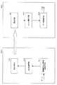
本発明の光通信装置としての送信機および受信機の一実施例を図3を参照して説明する。図3は、通信データを光信号として出力する光出力手段313を備えた送信機310と、光信号を受信する受光手段321を備えた受信機320の構成を示している。
【0044】
ここでは、通信データに基づいて変調された信号からなる可視光波長領域の光信号を送受信データとした例を示す。従って、送信機310の光出力手段313は、可視光を出力する例えば照明手段、あるいはディスプレイ手段(例えば強誘電性LCD、あるいは、有機ELディスプレイ等)によって構成可能である。一方、受信機320の受光手段321は、可視光波長領域の光を受信し電機信号に変換する例えばCCD、CMOSイメージセンサーによって構成される。
【0045】
送信機310中の光出力手段313は、受信機320に対して光変調信号を送信するのみならず、照明として、あるいは画像表示ディスプレイとしての期能を有し、照明としてしようしながら、あるいは画像表示を実行しながらのデータ通信を実行し、輝度レベルを低下させない通信を実現する。
【0046】
なお、図には示していないが、受信機320の受光手段321は、例えばレンズを含む光学系を介して送信機310の光出力手段313の出力する光データをセンサー面に結像する。
【0047】
送信機310の変調信号生成手段311は、例えばビット情報列によって構成される通信データシーケンスを輝度変化情報に変調し、変調信号シーケンスを生成する。出力制御手段312は、変調信号生成手段311において生成した変調信号シーケンスに対応する出力制御信号を光出力手段313に出力し、光出力手段313は、出力制御信号に基づいて、通信データシーケンスに対応した輝度変化を発生させて、データ出力を行なう。
【0048】
送信機310の変調信号生成手段311の実行する変調方式について、図4を用いて説明する。本実施例において、適用する変調方式は、反転PPM変調方式であり、先に図2を参照して説明した従来のPPM方式におけるパルスのオン/オフを反転させた構成を持つ、
【0049】
先に図1を参照して説明したPPM変調方式は、各フレームにおいて設定可能な複数のパルス位置のいずれか1つの位置にパルスを発生してデータを表現する構成である。例えば図1(c)の4−PPM構成では、フレーム中の第1スロットがオン=00、フレーム中の第2スロットがオン=01、フレーム中の第3スロットがオン=10、フレーム中の第4スロットがオン=11を、それぞれ示していた。
【0050】
本実施例においては、これら各スロットのオン(High)/オフ(Low)を反転させる変調方式、すなわち、反転PPM変調方式を実行する。
【0051】
図4(a)は、通信データシーケンスを示し、(b)〜(d)は、異なる態様の反転パルス位置変調(PPM)方式による光データシーケンスを示している。
【0052】
(b)に示す例は、フレーム(シンボル長)を2つのパルス幅に設定した反転2−PPMによるデータシーケンス例である。パルスの存在する部分が、光信号の存在する部分あるいは輝度レベルが高い部分、パルスの存在しない部分が、光信号の存在しない部分あるいは輝度レベルが低い部分である。2つのパルス幅に設定した領域の前半のパルス設定領域(前半スロット)にパルスがない場合を[1]、後半のパルス設定領域(後半スロット)にパルスがない場合を[0]として設定する。各フレームにおけるパルス配列を識別することにより、データが判別される。
【0053】
(c)に示す例は、フレームを4つのパルス幅に設定した例であり、各フレームにおいて、[00]、[01]、[10]、[11]の4種類のデータを示す。4つのパルス幅に設定した領域の第1番目のパルス設定領域(第1スロット)にパルスがない場合を[11]、第2番目のパルス設定領域(第2スロット)にパルスがない場合を[10]、第3番目のパルス設定領域(第3スロット)にパルスがない場合を[01]、第4番目のパルス設定領域(第4スロット)にパルスがない場合を[00]として設定する。各フレームにおけるパルス配列を識別することにより、データが判別される。
【0054】
(d)に示す例は、フレームを8つのパルス幅に設定した例であり、各フレームにおいて、[000]〜[111]の8種類のデータを示す。8つのパルス幅に設定した領域の何番目のパルス設定領域にパルスがないかによって、[000]〜[111]の8種類のデータのいずれかが示される。
【0055】
このように、反転パルス位置変調(Inverted PPM)方式では、従来のPPM方式による光信号列に比較して、高いデューテイ、すなわちON(High)となったパルスが多く存在する。
【0056】
フレームを2パルス間隔として設定した反転2−PPM方式では、従来の2−PPM方式と、パルス密度が変わらないが、フレームを4パルス間隔として設定した反転4−PPM方式では、従来の4−PPM方式と比較して、パルス密度が1/4から3/4に変化し、結果として、照明光の明るさ、あるいはディスプレイの輝度レベルの低下が抑制され、反転4−PPM方式を適用することにより、照明あるいはディスプレイの使用状態に大きな変化をもたらすことなく、通信データの送信が可能となる。
【0057】
さらに、フレームを8パルス間隔として設定した反転8−PPM方式では、従来の8−PPM方式と比較して、パルス密度が1/8から7/8に変化し、反転4−PPM方式の場合より、さらに、照明光の明るさ、あるいはディスプレイの輝度レベルの低下が抑制される。このように反転PPM方式を適用することにより、照明あるいはディスプレイの通常の使用状態を維持したまま、通信データを送信することが可能となる。
【0058】
従来のPPM方式と、反転PPM方式について、デューテイサイクルで比較すると、以下のようになる。
2−PPM:50%,反転2−PPM:50%
4−PPM:25%,反転4−PPM:75%
8−PPM:12.5%,反転8−PPM:87.5%
である。
【0059】
一般式で示すと、反転n−PPMにおいて、そのデューテイサイクルは、(1−(1/n))×100%であり、従来のn−PPMでは、デューテイサイクルは、100/nとなる。従って、nが大であるほど、反転n−PPMにおいてはデューテイサイクルが大となり、照明光の明るさ、あるいはディスプレイの輝度レベルの低下が小さくなる。
【0060】
送信機310が反転PPM変調データを光出力手段313を介して表示、送信した場合、受信機320側ではCCD、CMOS等の受光素子センサーを持つ受光手段321から信号を取り出し、フレーム定義位置判別のためのフレーム同期処理の後、各フレームのスロット(パルス設定領域)のパルス位置を検出することで復調、すなわち通信データの取得を行う。
【0061】
すなわち、受信機320は、受光手段321の受光素子の受信光信号の解析を実行し、受光素子の解析に基づいて反転PPM変調データシーケンスを取得するとともに、取得した反転PPM変調データシーケンスに対応する通信データシーケンス(ビット列)を取得する処理を実行する信号解析手段を有する。
【0062】
信号解析手段は、復調対象の変調信号、すなわち反転PPM信号の復調処理構成を有する。図3には、反転PPM変調信号の復調処理を実行する信号解析手段として、スロット積分手段322、データ変換手段323からなる構成を示している。
【0063】
図3に示す構成を持つ信号解析手段の処理について説明する。スロット積分手段322において、フレームのスロット位置を判別するためクロックからクロック情報を入力して、受光手段321において受信した反転PPM信号を構成する各スロットの積分処理を行なう。すなわち、予め定められた各ビット情報に対応するスロットパータン(コード)と受信信号とのマッチング積分を行い、積分値が最大のコードを最尤のコードとして選択し、データ変換手段323において、取得コードに基づくデータ(ビット情報)取得処理を行なう。
【0064】
このように、本発明の反転PPM信号を用いた光データ通信においては、高いデューテイサイクルを維持した通信が可能となり、例えば照明装置あるいはディスプレイ装置において可視光を適用した通信を行なう場合に、照明の照度を低下させることなく、またディスプレイの輝度レベルを低下させることなく通信を実行することが可能となる。
【0065】
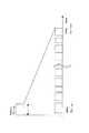
また、反転PPM信号によってデータを送受信することで、受信機における受信信号のエラーレートも低下させることが可能となる。図5を参照して、反転PPM信号と、従来のPPM信号によるデータ送受信におけるエラー率について説明する。
【0066】
図5は、X軸に受信機における信号レベル(W)、Y軸に受信データのビットエラー率(BER)を示した図であり、コンピュータを用いたシミュレーション結果を示す。白丸が従来のパルス位置変調(PPM)方式による光通信、黒丸が本発明の反転パルス位置変調(反転PPM)方式による光通信のプロットを示している。なお、シミュレーションは、受信機におけるノイズ=0dBm(1e−3Watt)とし、パルス位置変調(PPM)および反転パルス位置変調(反転PPM)における最大パワーレベルは等しいものとして実行した。
【0067】
図5から理解されるように、反転パルス位置変調(反転PPM)方式による光通信の場合のほうが、従来のパルス位置変調(PPM)方式による光通信に比較して、同じ信号レベルにおいて、低いエラー率となっており、正確なデータ通信が実現される。
【0068】
次に、送信機310の光出力手段313としてLCD等のディスプレイ装置を用い、視覚可能な画像をディスプレイ装置に表示しながら表示画像に重畳して通信用データを表示、送信する構成について説明する。ここでは、ディスプレイ装置のうち、輝度制御をピクセルのオンの時間の長短によって制御する方式(フィールドシーケンシャル方式)を用いた表示処理方式による構成を持つ装置に、データを重畳する処理について説明する。ただし、本発明はフィールドシーケンシャル方式に限らずあらゆる表示方式に適応可能である。
【0069】
図6を参照して、一般のフィールドシーケンシャル方式によるカラー画像の表示方法について説明する。フィールドシーケンシャル方式では、ディスプレイを構成する各ピクセルにおいて、各ピクセル表示色に従ってR,G,BそれぞれのON/OFF時間を設定したフレームを連続して出力することにより、各色を表示する。すなわち、各ピクセルのR,G,Bの輝度はそれぞれのオン時間の長短によってコントロールされる。
【0070】
図6に示すように、各ピクセルに対応して、Rタイムフレーム、Gタイムフレーム、Bタイムフレームが、順次設定され、各フレームにおいて、R,G,BのそれぞれのON時間として、Rオンフレーム、Gオンフレーム、Bオンフレーム、各RGBのオンフレームの設定時間に基づいて各ピクセルの表示色が決定する。この処理により、ディスプレイを構成するピクセルの色が設定され、ディスプレイ全体として画像データが表示されることになる。
【0071】
このようなフィールドシーケンシャル方式によるカラー画像表示方式において、図4を用いて説明した反転PPM変調方式に従った光パルスデータを表示画像に重畳する。
【0072】
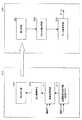
図7に示す送信機310の変調信号生成手段311が、通信データを構成するビット情報に基づいて図4に示す反転PPM変調信号を生成する。さらに、図7に示す重畳処理手段411において、視覚可能な画像信号に反転PPM変調信号を重畳し、重畳信号を生成する。
【0073】
重畳処理手段411による信号生成処理について、図8を参照して説明する。先に図6を参照して説明したように、視覚画像は、フィールドシーケンシャル方式によるカラー画像表示であり、R,G,BそれぞれのON/OFF時間を設定したフレームを連続して出力することにより各ピクセルの色が表示される。
【0074】
通信データは、各タイムフレーム中のオンフレームの領域を利用して重畳される。図には、Rオンフレームに通信データを重畳した例を示している。Rオンフレーム内に例えば4スロット(2ビット)からなる反転PPM変調データからなるPPMフレームを連続して複数組み込む構成とする。
【0075】
すなわち、図7の重畳処理手段411は、画像データにおいてR,G,Bの各信号がオンとなった位置において、通信データの反転PPM変調信号を重畳し、重畳信号を生成する。ここでの重畳処理は、反転PPM信号のスロットがオンとなった位置では、画像信号のオン状態を維持し、反転PPM信号のスロットがオフとなった位置では、画像信号のRまたはGまたはBの信号をオフとする設定である。
【0076】
図7の出力制御手段312は、重畳処理手段411の生成した重畳信号に基づいて、光出力手段313、すなわちディスプレイに対するピクセル輝度制御信号を出力する。
【0077】
前述のように、反転PPM信号は、例えば図4を参照して説明した4スロット構成を持つ反転4−PPMにおいて、いずれの信号(00〜11)においても、オン:オフの割合は3:1であり、全体としての輝度の減少は少なく抑えることができる。
【0078】
また、ディスプレイとして強誘電性LCDを用いれば、その応答時間は100マイクロセカンド前後であり、反転PPM信号のスロット単位を100マイクロセカンド前後に設定することが可能であり、画像信号としての劣化レベルは視覚上ほとんど問題のないレベルに抑えることが可能となる。
【0079】
図9にRオンフレームに通信データを重畳した場合のRオンフレームの信号変化を示す。前述のように、Rオンフレームに対して、反転PPM変調信号が重畳されることにより、3/4がオン、1/4がオフとなったPPMフレームをn個格納し、データとしては、2×nビットの情報を格納したPPMフレームをRフレーム中に重畳することができる。
【0080】
本方式では、フィールドシーケンシャル方式によるカラー画像表示におけるR,G,Bそれぞれのオンフレームに連続して通信データに基づくPPMフレームを重畳することになるので、R,G,Bすべてのオンフレームにおいて、3/4がオン、1/4がオフとなったPPMフレームが重畳され、R,G,Bとも同様の輝度変化が発生し、偏った色の変化は発生しない。
【0081】
なお、通信データを重畳する場合に画像データ自体の調整を予め実行する構成としてもよい。例えば、R,G,Bの輝度レベルを通信データの重畳によって低下する分、予めアップするように重畳処理以前に補正する。
【0082】
具体的には、例えば4スロットのPPMフレームを用いる場合は、通信データの重畳により、3/4の輝度レベル低下が予測されるので、オリジナル画像データのR,G,Bレベルを4/3倍に設定する補正を実行した後、通信データを重畳する構成とすれば、通信データの重畳による画像データの劣化を抑えることができる。
【0083】
次に、図10以下を参照して、送信機の光出力手段として、ディスプレイを適用した構成例について説明する。図10に示す例は、ビデオプロジェクタ511を用いて、通信データを重畳した画像を投影し、投影画像を二次元センサーを備えた受像機512,514において受信し、受信データ(画像)をPC等のデータ処理装置513,515において処理することによって通信データを取得する構成である。
【0084】
ビデオプロジェクタ511は、例えばインターネットを介して通信データを受信し、これを、予めビデオプロジェクタ511内のメモリに格納した画像データに重畳して、スクリーンに投影する。この投影画像を各受像機において受信し、受信したデータをデータ処理装置としてのPCに出力し、上述したPPM信号の解析により、画像中のPPM変調信号を取り出して、取り出した信号に基づいてデータ、すなわち各PPMフレームに設定されたビット情報を取得する。
【0085】
この例ではビデオプロジェクタ511が、例えば家庭内でのワイヤレスのアクセスポイントとなっており、このビデオプロジェクタ511はインターネットなどから高速に取り込まれたデータを、表示すべき画像に畳み込み、表示をする。人間が画像を見ても変調されていない画像と何ら変わらない画像を見ることができる。
【0086】
各受像機512,515では、レンズ等によって構成される光学系を介して画像が光センサー上に撮り込まれ、取得データが、PC等のデータ処理装置に出力され、センサーのとり込みデータ(輝度変化データ)について復調処理がなされる。
【0087】
図11は、ディスプレイを有するビデオカメラレコーダ間で通信データを重畳した画像により通信を実行する例を示している。ここでは各ビデオカメラレコーダ521,523には液晶モニター522,524が備えられ、液晶モニターに通信データを重畳した画像データを表示する。
【0088】
各ビデオカメラレコーダ521,523は、カメラ部を介して、液晶モニター522,524に表示された画像を撮り込み、カメラ内部の二次元センサーにおいて、各画素の輝度変化情報を読み取り、カメラ内部のデータ処理手段において、輝度変化情報に基づく通信データの取得処理を行なう。各ビデオカメラレコーダ521,523は、ディスプレイとしては、例えば強誘電性ディスプレイ、あるいは有機ELディスプレイ等の高速変調が可能な素子が使用される。図に示すように2台のビデオカメラレコーダを合い向かわせることにより、可視光を用いたデータ送受信を行うことが出来る。
【0089】
図12は、カメラ機能およびディスプレイ機能を持つ携帯電話531,541間での通信処理例を示している。それぞれの携帯電話531,541は、カメラ部533,543を介して、それぞれ互いのディスプレイ532,542に表示された画像を撮り込み、携帯電話531,541内部のカメラ部533,543において、画素の輝度変化情報を読み取り、携帯電話531,541内部のデータ処理手段において、輝度変化情報に基づく通信データの取得処理を行なう。
【0090】
それぞれの携帯電話531,541のディスプレイは、例えば強誘電性ディスプレイ、あるいは有機ELディスプレイ等の高速変調が可能な素子を使用することで、高速データ通信が可能となる。
【0091】
上述した各機器において、取得画像からのデータ取得処理、通信データの変調処理、あるいは画像に対する変調データの重畳処理を実行するデータ処理手段のハードウェア構成例を図13を参照して説明する。データ処理手段は、例えばPC等によって構成可能であるが、上述したように、カメラ、携帯電話、ビデオプロジェクタ等の各機器に組み込むことも可能である。図13を参照して、上述した処理を実行するデータ処理手段構成を説明する。
【0092】
CPU(Central processing Unit)711は、各種アプリケーションプログラムや、OS(Operating System)を実行するプロセッサである。上述の通信データの変調処理、画像データに対するデータ重畳処理、あるいは受信画像についてのデータ取得処理を実行する。ROM(Read−Only−Memory)712は、CPU711が実行するプログラム、あるいは演算パラメータとしての固定データを格納する。RAM(Random Access Memory)713は、CPU711の処理において実行されるプログラム、およびプログラム処理において適宜変化するパラメータの格納エリア、ワーク領域として使用される。
【0093】
HDD714はハードディスクの制御を実行し、ハードディスクに対する各種データ、プログラムの格納処理および読み出し処理を実行する。バス720はPCI(Peripheral Component Internet/Interface)バス等により構成され、各モジュール、入出力インタフェース721を介した各入出力装置とのデータ転送を可能にしている。
【0094】
入力部715は、例えば前述したCMOS等の高速応答性のセンサーであり、センサーによって撮り込まれた画像に基づいて、CPU711において、データ取得プログラムが実行されて通信データが取得される。出力部716は、例えば前述した照明、ディスプレイ(例えば強誘電性ディスプレイ、あるいは有機ELディスプレイ)等であり、例えばCPU711において通信データの重畳処理プログラムが実行されて通信データを重畳した画像が表示される。
【0095】
通信部717は、例えばインターネット、LAN等の各種ネットワークを介した通信を実行する通信処理部であり、画像データ、あるいは画像に重畳すべき通信データ、あるいは通信データを重畳済みの画像データの送受信処理に適用される。
【0096】
ドライブ718は、フロッピーディスク、CD−ROM(Compact Disc Read Only Memory),MO(Magneto optical)ディスク,DVD(Digital Versatile Disc)、磁気ディスク、半導体メモリなどの記録媒体719の記録再生を実行するドライブであり、各記録媒体719からのプログラムまたはデータ再生、記録媒体719に対するプログラムまたはデータ格納を実行する。
【0097】
各記憶媒体に記録されたプログラムまたはデータを読み出してCPU711において実行または処理を行なう場合は、読み出したプログラム、データは入出力インタフェース721、バス720を介して例えば接続されているRAM713に供給される。
【0098】
以上、特定の実施例を参照しながら、本発明について詳解してきた。しかしながら、本発明の要旨を逸脱しない範囲で当業者が該実施例の修正や代用を成し得ることは自明である。すなわち、例示という形態で本発明を開示してきたのであり、限定的に解釈されるべきではない。本発明の要旨を判断するためには、冒頭に記載した特許請求の範囲の欄を参酌すべきである。
【0099】
なお、明細書中において説明した一連の処理はハードウェア、またはソフトウェア、あるいは両者の複合構成によって実行することが可能である。ソフトウェアによる処理を実行する場合は、処理シーケンスを記録したプログラムを、専用のハードウェアに組み込まれたコンピュータ内のメモリにインストールして実行させるか、あるいは、各種処理が実行可能な汎用コンピュータにプログラムをインストールして実行させることが可能である。
【0100】
例えば、プログラムは記憶媒体としてのハードディスクやROM(Read Only Memory)に予め記録しておくことができる。あるいは、プログラムはフレキシブルディスク、CD−ROM(Compact Disc Read Only Memory),MO(Magneto optical)ディスク,DVD(Digital Versatile Disc)、磁気ディスク、半導体メモリなどのリムーバブル記録媒体に、一時的あるいは永続的に格納(記録)しておくことができる。このようなリムーバブル記録媒体は、いわゆるパッケージソフトウエアとして提供することができる。
【0101】
なお、プログラムは、上述したようなリムーバブル記録媒体からコンピュータにインストールする他、ダウンロードサイトから、コンピュータに無線転送したり、LAN(Local Area Network)、インターネットといったネットワークを介して、コンピュータに有線で転送し、コンピュータでは、そのようにして転送されてくるプログラムを受信し、内蔵するハードディスク等の記憶媒体にインストールすることができる。
【0102】
また、明細書に記載された各種の処理は、記載に従って時系列に実行されるのみならず、処理を実行する装置の処理能力あるいは必要に応じて並列的にあるいは個別に実行されてもよい。
【0103】
【発明の効果】
以上、説明したように、本発明の構成によれば、パルス位置変調(PPM)におけるオン/オフ位置を反転させた反転パルス位置変調(反転PPM)処理を通信データシーケンスに対して施して反転PPM信号シーケンスを適用した光通信を行なう構成としたので、高いデューテイサイクル、すなわちパルスのオン時間が長いパルスデータを適用した通信が可能となり、例えば照明装置あるいはディスプレイ装置において可視光を適用した通信を行なう場合に、照明の照度を低下させることなく、またディスプレイの輝度レベルを低下させることなく通信を実行することが可能となる。
【0104】
また、本発明の構成によれば、視覚可能な画像データに対して、通信データに基づく変調信号シーケンスを重畳し出力することが可能であり、通常の画像データとともに通信データを送信することが可能となる。
【0105】
また、本発明の構成によれば、反転PPM信号によってデータを送受信する構成としたことにより、受信機における受信信号のエラーレートの低下が可能となり、正確なデータ通信が実現される。
【図面の簡単な説明】
【図1】光通信におけるデータシーケンスと光信号の対応例を示す図である。
【図2】光通信における光データの送受信構成例を示す図である。
【図3】本発明に係る光通信装置における送信機および受信機の構成を示すブロック図である。
【図4】本発明に係る光通信装置において適用可能な反転PPM変調方式について説明する図である。
【図5】本発明に係る光通信装置において適用可能な反転PPM方式と従来のPPM方式についてのビットエラー率の比較図である。
【図6】フィールドシーケンシャル表示方式の処理について説明する図である。
【図7】本発明に係る光通信装置において、画像に通信データを重畳してデータ送受信を行なう送信機および受信機の構成を示すブロック図である。
【図8】フィールドシーケンシャル表示方式に通信データを重畳する処理について説明する図である。
【図9】フィールドシーケンシャル表示方式に通信データを重畳する処理について説明する図である。
【図10】本発明に係る光通信装置の適用例について説明する図である。
【図11】本発明に係る光通信装置の適用例について説明する図である。
【図12】本発明に係る光通信装置の適用例について説明する図である。
【図13】本発明に係る光通信装置のデータ処理手段構成例について示す図である。
【符号の説明】
110 送信機
120 受信機
310 送信機
311 変調信号生成手段
312 出力制御手段
313 光出力手段
320 受信機
321 受光手段
322 スロット積分手段
323 データ変換手段
411 重畳処理手段
511 ビデオプロジェクタ
512,514 受像機
513,515 データ処理装置
521,523 ビデオカメラレコーダー
522,524 液晶モニター
531,541 携帯電話
532,542 ディスプレイ
533,543 カメラ
711 CPU
712 ROM
713 RAM
714 HDD
715 入力部
716 出力部
717 通信部
718 ドライブ
719 記憶媒体
720 バス
721 入出力インタフェース[0001]
TECHNICAL FIELD OF THE INVENTION
The present invention relates to an optical communication device, an optical communication data output method, an optical communication data analysis method, and a computer program. More specifically, the present invention relates to an apparatus and a method for performing optical communication to which an improved pulse position modulation (PPM) method is applied, and more particularly to an optical communication apparatus and an optical communication suitable for optical communication in a visible light region. The present invention relates to a data output method, an optical communication data analysis method, and a computer program.
[0002]
[Prior art]
Recently, wireless communication using light has been used in various fields. Since wireless (wireless) communication using light or radio waves does not require a cable as a data transmission path, for example, communication between portable devices, mutual communication between devices such as PCs and PDAs, or between a PC and a printer or It is used in various inter-device communication such as communication with a display and other peripheral devices. In particular, optical communication is lower in cost than a communication method using radio waves, and is not affected by electromagnetic radiation noise.
[0003]
As a conventional optical communication system, there is a configuration in which, for example, a pulse signal train whose light intensity is changed by infrared light or the like is generated, and the pulse signal is analyzed on the receiver side. In optical communication, a modulated signal by such light intensity modulation processing is often used.
[0004]
As the light intensity modulation signal, for example, modulated light of light emitted from an LED (Light Emitting Diode) or a laser diode (LD) is output, and data is acquired by performing intensity analysis on the receiving side. In information transmission in optical communication, coherency related to the wavelength of light is rarely used, and light intensity is mainly used. This is because the wavelength of the optical signal is 1014 This is because coherent detection is difficult because the frequency is higher than Hz, and the demodulation process of the intensity modulation signal is simple and the processing load on the receiving side is small.
[0005]
Typical light intensity modulation methods include, for example, a method of determining the luminance itself based on communication data, such as On Off Keying (OOK), or information based on the pulse position of a luminance change pulse. There is a pulse position modulation (PPM) method in which a PPM is placed.
[0006]
An on-off keying (OOK) and a pulse position modulation (PPM) scheme will be described with reference to FIG.
[0007]
FIG. 1A shows a communication data sequence, FIG. 1B shows an optical data sequence based on an on-off keying (OOK) system, and FIGS. 1C to 1E show optical systems based on a different form of pulse position modulation (PPM) system. 4 shows a data sequence.
[0008]
On-off keying (OOK) shown in (b) is based on a pulse generation rule that generates a pulse when the communication data bit is [1] and does not generate a pulse when the communication data bit is [0]. This is a method of transmitting and receiving a pulse train corresponding to communication data by controlling the light intensity to be output based on the data sequence. For example, if the bit string of the communication data is 1101, the setting pulse is set according to the bit string, such as high, high, low, high.
[0009]
(C) to (e) show an example of data transfer processing by a pulse position modulation (PPM) method. The pulse position modulation (PPM) is a signal that generates a pulse train based on different luminance levels, and data is read based on a pulse train set within a predetermined symbol length.
[0010]
The example shown in (c) is an example in which the symbol length (or frame) is set to two pulse widths, and the portion where the pulse exists is the portion where the optical signal exists or the portion where the luminance level is high, or the pulse does not exist. The portion is a portion where no optical signal exists or a portion where the luminance level is low. The case where there is a pulse in the first half of the region set to two pulse widths is set as [1], and the case where there is a pulse in the second half is set as [0]. The data is determined by identifying the pulse arrangement at each symbol length.
[0011]
The example shown in (d) is an example in which a frame is set to four pulse widths, and shows four types of data of [00], [01], [10], and [11] in each frame. [11] indicates the case where the first pulse is present in the region set to the four pulse widths, [10] indicates the case where the second pulse is present, [01] indicates the case where the third pulse is present, and The case where there is a pulse at the th is set as [00]. Data is determined by identifying the pulse arrangement in each frame.
[0012]
The example shown in (e) is an example in which a frame is set to eight pulse widths, and shows eight types of data [000] to [111] in each frame. Either of the eight types of data [000] to [111] is indicated depending on the position of the pulse in the region set to the eight pulse widths.
[0013]
It is assumed that such optical communication based on on-off keying (OOK) or pulse position modulation (PPM) signal is performed by applying, for example, visible light.
[0014]
As shown in FIG. 2, a
[0015]
The light emitting unit of the transmitter is a light emitting unit that outputs visible light, and can be used, for example, for daily lighting such as indoor lights and outdoor lights. Alternatively, application as a display for image output is also possible.
[0016]
However, when the above-described optical communication using the on-off keying (OOK) or the pulse position modulation (PPM) signal is performed while being applied as a daily light or as a display for outputting an image, light is emitted only in an area where a pulse is present. The light emission is stopped in a region where there is no pulse. As a result, the brightness as illumination decreases, and the luminance as a display decreases.
[0017]
That is, it is difficult to apply the light output means as illumination while performing communication using visible light, or to apply it as a display for image output.
[0018]
[Problems to be solved by the invention]
The present invention has been made in view of the above-described problems.For example, in a transmission / reception configuration of optical data to which visible light is applied, a reduction in luminance is suppressed, and a light output unit is applied as illumination or used for image output. It is an object of the present invention to provide an optical communication device, an optical communication method, and a computer program which can be applied as a display.
[0019]
[Means for Solving the Problems]
According to a first aspect of the present invention,
An optical communication device as a transmitter for outputting optical communication data,
Modulation signal generating means for performing an inverted pulse position modulation (inverted PPM) process in which an on / off position in pulse position modulation (PPM) is inverted on a communication data sequence to generate an inverted PPM signal sequence;
Output control means for outputting an output control signal corresponding to the inverted PPM signal sequence generated by the modulation signal generation means;
Output means for outputting an optical signal sequence corresponding to an inverted PPM signal sequence based on the communication data sequence based on an output control signal output by the output control means;
An optical communication device comprising:
[0020]
Further, in one embodiment of the optical communication apparatus according to the present invention, the optical signal sequence output from the output means is an optical signal having a wavelength in a visible light region.
[0021]
Further, in one embodiment of the optical communication apparatus according to the present invention, the output means is a lighting means for irradiating visible light.
[0022]
Further, in one embodiment of the optical communication apparatus according to the present invention, the output means is a display for outputting an image.
[0023]
Further, in one embodiment of the optical communication apparatus according to the present invention, the optical communication apparatus further includes a superimposing unit that superimposes an inverted PPM signal sequence generated by the modulation signal generating unit on the image data to generate a superimposed signal. Processing means, wherein the output control means outputs an output control signal corresponding to the superimposed signal generated by the superimposition processing means as a pixel luminance control signal of the display.
[0024]
Further, in one embodiment of the optical communication apparatus of the present invention, the superimposition processing means is configured to execute a process of superimposing a modulation signal sequence on an on-frame of each time frame of image data according to a field sequential method. It is characterized by.
[0025]
Further, a second aspect of the present invention provides
A light-receiving means having a light-receiving element, a light-receiving signal analysis of the light-receiving element, a modulation signal sequence corresponding to the light-receiving signal pattern based on the light-receiving signal analysis, and a communication corresponding to the obtained modulation signal sequence. An optical communication device as a receiver having a signal analysis unit that performs a process of acquiring a data sequence,
The signal analysis means,
As the modulation signal sequence, an inverted pulse position modulation (PPM) signal obtained by performing on / off inversion processing in pulse position modulation (PPM) is obtained, and the inverted pulse position is obtained by analyzing the inverted pulse position modulation (PPM) signal. An optical communication apparatus is characterized in that it is configured to execute a process of acquiring a communication data sequence corresponding to a modulated (inverted PPM) signal.
[0026]
Further, in one embodiment of the optical communication apparatus according to the present invention, the light receiving means includes a signal obtained by superimposing an inverted pulse position modulation (inverted PPM) signal sequence on an on-frame of each time frame of image data according to a field sequential system. Receiving, the signal analysis means is configured to acquire an inversion pulse position modulation (inversion PPM) signal sequence during an on-frame of each time frame and execute analysis.
[0027]
Further, a third aspect of the present invention provides
An optical communication data output method in a transmitter for outputting optical communication data,
A modulated signal generating step of performing an inverted pulse position modulation (PPM) process in which an on / off position in the pulse position modulation (PPM) is inverted on the communication data sequence to generate an inverted PPM signal sequence;
An output control step of outputting an output control signal corresponding to the inverted PPM signal sequence generated in the modulation signal generation step;
An output step of outputting an optical signal sequence corresponding to an inverted PPM signal sequence based on the communication data sequence based on the output control signal output in the output control step;
An optical communication data output method characterized by having:
[0028]
Further, in one embodiment of the optical communication data output method according to the present invention, the optical signal sequence output in the output step is an optical signal having a wavelength in a visible light region.
[0029]
Further, in one embodiment of the optical communication data output method of the present invention, the output step is a step of applying an illuminating means for irradiating visible light and outputting an optical signal sequence based on visible light.
[0030]
Further, in one embodiment of the optical communication data output method according to the present invention, the output step is a step of outputting an optical signal sequence by visible light by applying a display for outputting an image.
[0031]
Further, in one embodiment of the optical communication data output method according to the present invention, the optical communication data output method further includes the step of superimposing the inverted PPM signal sequence generated in the modulation signal generation step on the image data to generate a superimposed signal. The output control step outputs an output control signal corresponding to the superimposed signal generated in the superimposition processing step as a pixel luminance control signal of the display.
[0032]
Further, in one embodiment of the optical communication data output method of the present invention, the superimposing processing step is configured to execute a process of superimposing a modulation signal sequence on an on-frame of each time frame of image data according to a field sequential method. There is a feature.
[0033]
Further, a fourth aspect of the present invention provides
An optical communication data analysis method for receiving and analyzing optical communication data,
A light receiving step of receiving an optical signal in light receiving means having a light receiving element;
By analyzing the optical signal, having a signal analysis step of performing a process of obtaining a communication data sequence,
The signal analysis step includes:
An inversion pulse position modulation (inversion PPM) signal obtained by performing on / off inversion processing in pulse position modulation (PPM) is obtained based on the received light signal of the light receiving unit, and the inversion pulse position modulation (inversion PPM) signal is analyzed. And performing a process of obtaining a communication data sequence corresponding to the inverted pulse position modulation (inverted PPM) signal.
[0034]
Further, in one embodiment of the optical communication data analysis method of the present invention, the light receiving step includes superimposing an inverted pulse position modulation (inverted PPM) signal sequence on an on-frame of each time frame of image data according to a field sequential method. A signal receiving step, wherein the signal analyzing step obtains an inverted pulse position modulation (inverted PPM) signal sequence during an on-frame of each of the time frames and performs analysis.
[0035]
Furthermore, a fifth aspect of the present invention provides
A computer program for performing optical communication data output processing in a transmitter that performs output of optical communication data,
A modulated signal generating step of performing an inverted pulse position modulation (PPM) process in which an on / off position in the pulse position modulation (PPM) is inverted on the communication data sequence to generate an inverted PPM signal sequence;
An output control step of outputting an output control signal corresponding to the inverted PPM signal sequence generated in the modulation signal generation step;
An output step of outputting an optical signal sequence corresponding to an inverted PPM signal sequence based on the communication data sequence based on the output control signal output in the output control step;
A computer program characterized by having:
[0036]
Further, a sixth aspect of the present invention provides
A computer program for performing optical communication data analysis processing for receiving and analyzing optical communication data,
A light receiving step of receiving an optical signal in light receiving means having a light receiving element;
By analyzing the optical signal, having a signal analysis step of performing a process of obtaining a communication data sequence,
The signal analysis step includes:
An inversion pulse position modulation (inversion PPM) signal obtained by performing on / off inversion processing in pulse position modulation (PPM) is obtained based on the received light signal of the light receiving unit, and the inversion pulse position modulation (inversion PPM) signal is analyzed. Executing a process of obtaining a communication data sequence corresponding to an inverted pulse position modulation (PPM) signal by the computer program.
[0037]
[Action]
According to the configuration of the present invention, an optical communication in which an inverted PPM signal sequence is applied to a communication data sequence by performing an inverted pulse position modulation (inverted PPM) process in which an on / off position in pulse position modulation (PPM) is inverted. , A high duty cycle, that is, communication using pulse data with a long pulse on time can be applied. For example, when performing communication using visible light in a lighting device or a display device, the illuminance of the illumination It is possible to execute communication without lowering the brightness and without lowering the luminance level of the display.
[0038]
Further, according to the configuration of the present invention, it is possible to superimpose a modulated signal sequence based on communication data on visible image data and output the same, and to transmit communication data together with normal image data. It becomes.
[0039]
Further, according to the configuration of the present invention, since the data is transmitted and received by the inverted PPM signal, the error rate of the received signal in the receiver can be reduced, and accurate data communication can be realized.
[0040]
The computer program of the present invention is provided, for example, in a computer-readable format for a general-purpose computer system capable of executing various program codes, in a storage medium or communication medium such as a CD, FD, or MO. And a computer program that can be provided by a communication medium such as a network. By providing such a program in a computer-readable format, processing according to the program is realized on a computer system.
[0041]
Further objects, features, and advantages of the present invention will become apparent from the following detailed description based on embodiments of the present invention and the accompanying drawings. In this specification, the term “system” refers to a logical set of a plurality of devices, and is not limited to a device having each configuration in the same housing.
[0042]
BEST MODE FOR CARRYING OUT THE INVENTION
Hereinafter, an optical communication device and an optical communication method according to the present invention will be described in detail with reference to the drawings.
[0043]
One embodiment of a transmitter and a receiver as an optical communication device of the present invention will be described with reference to FIG. FIG. 3 shows a configuration of a
[0044]
Here, an example is shown in which an optical signal in the visible light wavelength region composed of a signal modulated based on communication data is used as transmission / reception data. Therefore, the
[0045]
The light output means 313 in the
[0046]
Although not shown, the
[0047]
The modulation signal generation means 311 of the
[0048]
The modulation method executed by the modulation signal generation means 311 of the
[0049]
The PPM modulation method described above with reference to FIG. 1 has a configuration in which a pulse is generated at any one of a plurality of pulse positions that can be set in each frame to represent data. For example, in the 4-PPM configuration of FIG. 1C, the first slot in the frame is ON = 00, the second slot in the frame is ON = 01, the third slot in the frame is ON = 10, and the third slot in the frame is ON = 10. Four slots indicated ON = 11, respectively.
[0050]
In the present embodiment, a modulation method for inverting ON (High) / OFF (Low) of each slot, that is, an inverted PPM modulation method is executed.
[0051]
FIG. 4A shows a communication data sequence, and FIGS. 4B to 4D show optical data sequences based on a different form of inverted pulse position modulation (PPM).
[0052]
The example shown in (b) is a data sequence example using inverted 2-PPM in which a frame (symbol length) is set to two pulse widths. A portion where a pulse exists is a portion where an optical signal exists or a portion with a high luminance level, and a portion where no pulse exists does not exist or a portion where a luminance level is low. The case where there is no pulse in the first half pulse setting region (first half slot) of the region set to two pulse widths is set as [1], and the case where there is no pulse in the second half pulse setting region (second half slot) is set as [0]. Data is determined by identifying the pulse arrangement in each frame.
[0053]
The example shown in (c) is an example in which a frame is set to four pulse widths, and shows four types of data of [00], [01], [10], and [11] in each frame. A case where there is no pulse in the first pulse setting region (first slot) of the region set to four pulse widths is [11], and a case where there is no pulse in the second pulse setting region (second slot) is [11]. 10], the case where there is no pulse in the third pulse setting area (third slot) is set as [01], and the case where there is no pulse in the fourth pulse setting area (fourth slot) is [00]. Data is determined by identifying the pulse arrangement in each frame.
[0054]
The example shown in (d) is an example in which a frame is set to eight pulse widths, and eight types of data [000] to [111] are shown in each frame. One of the eight types of data [000] to [111] is indicated depending on the number of the pulse setting area in the area set to the eight pulse widths.
[0055]
As described above, in the inverted pulse position modulation (Inverted PPM) system, there are many pulses that have a high duty, that is, ON (High), as compared with the optical signal train based on the conventional PPM system.
[0056]
In the inverted 2-PPM method in which the frame is set at two pulse intervals, the pulse density is the same as in the conventional 2-PPM method, but in the inverted 4-PPM method in which the frame is set at four pulse intervals, the conventional 4-PPM method is used. Compared with the scheme, the pulse density changes from 1/4 to 3/4, and as a result, a decrease in the brightness of the illumination light or the brightness level of the display is suppressed, and by applying the inverted 4-PPM scheme. Thus, communication data can be transmitted without causing a significant change in the use state of the lighting or the display.
[0057]
Further, in the inverted 8-PPM method in which a frame is set at an interval of 8 pulses, the pulse density changes from 1/8 to 7/8 as compared with the conventional 8-PPM method, and the pulse density changes more than in the case of the inverted 4-PPM method. Further, a decrease in the brightness of the illumination light or the luminance level of the display is suppressed. By applying the inverted PPM method in this manner, it is possible to transmit communication data while maintaining a normal use state of lighting or a display.
[0058]
A comparison between the conventional PPM method and the inverted PPM method in a duty cycle is as follows.
2-PPM: 50%, inverted 2-PPM: 50%
4-PPM: 25%, inverted 4-PPM: 75%
8-PPM: 12.5%, inverted 8-PPM: 87.5%
It is.
[0059]
In general terms, the duty cycle of the inverted n-PPM is (1- (1 / n)) × 100%, and the duty cycle of the conventional n-PPM is 100 / n. . Therefore, as n increases, the duty cycle in the inverted n-PPM increases, and the decrease in the brightness of the illumination light or the luminance level of the display decreases.
[0060]
When the
[0061]
That is, the
[0062]
The signal analysis means has a demodulation processing configuration for a demodulated modulation signal, that is, an inverted PPM signal. FIG. 3 shows a configuration including a
[0063]
The processing of the signal analyzing means having the configuration shown in FIG. 3 will be described. The
[0064]
As described above, in the optical data communication using the inverted PPM signal of the present invention, communication maintaining a high duty cycle can be performed. For example, when communication using visible light is performed in a lighting device or a display device, lighting It is possible to execute communication without lowering the illuminance of the display and without lowering the luminance level of the display.
[0065]
Further, by transmitting and receiving data using the inverted PPM signal, it is possible to reduce the error rate of the received signal in the receiver. With reference to FIG. 5, an error rate in data transmission / reception using an inverted PPM signal and a conventional PPM signal will be described.
[0066]
FIG. 5 is a diagram showing the signal level (W) in the receiver on the X-axis and the bit error rate (BER) of the received data on the Y-axis, and shows a simulation result using a computer. A white circle indicates a plot of optical communication based on the conventional pulse position modulation (PPM) method, and a black circle indicates a plot of optical communication based on the inverted pulse position modulation (inverted PPM) method of the present invention. The simulation was performed with the noise in the receiver set to 0 dBm (1e−3 Watt) and the maximum power levels in pulse position modulation (PPM) and inverted pulse position modulation (PPM) were equal.
[0067]
As can be understood from FIG. 5, in the case of the optical communication based on the inverted pulse position modulation (inverted PPM) method, a lower error is obtained at the same signal level as compared with the optical communication based on the conventional pulse position modulation (PPM) method. Rate, and accurate data communication is realized.
[0068]
Next, a configuration will be described in which a display device such as an LCD is used as the
[0069]
With reference to FIG. 6, a method of displaying a color image by a general field sequential method will be described. In the field sequential system, each color is displayed by continuously outputting frames in which ON / OFF times of R, G, and B are set in accordance with each pixel display color in each pixel constituting the display. That is, the luminance of R, G, B of each pixel is controlled by the length of each ON time.
[0070]
As shown in FIG. 6, an R time frame, a G time frame, and a B time frame are sequentially set for each pixel, and in each frame, an R on-frame is set as an ON time of each of R, G, and B. , G on-frame, B on-frame, and RGB on-frame are set based on the set time of each pixel. By this processing, the colors of the pixels constituting the display are set, and the image data is displayed on the entire display.
[0071]
In such a color image display method using the field sequential method, optical pulse data according to the inverted PPM modulation method described with reference to FIG. 4 is superimposed on a display image.
[0072]
Modulated signal generation means 311 of
[0073]
The signal generation processing by the superposition processing means 411 will be described with reference to FIG. As described above with reference to FIG. 6, the visual image is a color image display by a field sequential method, and continuously outputs frames in which ON / OFF times of R, G, and B are set. The color of each pixel is displayed.
[0074]
The communication data is superimposed using an on-frame area in each time frame. The figure shows an example in which communication data is superimposed on an R on-frame. For example, a plurality of PPM frames composed of inverted PPM modulation data composed of, for example, 4 slots (2 bits) are continuously incorporated in the R-on frame.
[0075]
That is, the
[0076]
The
[0077]
As described above, the inverted PPM signal has an on: off ratio of 3: 1 in any of the signals (00 to 11) in the inverted 4-PPM having the 4-slot configuration described with reference to FIG. Thus, a decrease in luminance as a whole can be suppressed to a small level.
[0078]
When a ferroelectric LCD is used as a display, the response time is about 100 microseconds, and the slot unit of the inverted PPM signal can be set to about 100 microseconds. It is possible to keep the level at which there is almost no problem visually.
[0079]
FIG. 9 shows a signal change of the R on-frame when the communication data is superimposed on the R on-frame. As described above, by superimposing the inverted PPM modulation signal on the R on-frame, n PPM frames in which オ ン is turned on and 1 / is turned off are stored. A PPM frame storing information of × n bits can be superimposed on the R frame.
[0080]
In this method, the PPM frame based on the communication data is superimposed continuously on each of the R, G, and B on-frames in the color image display by the field sequential method. A PPM frame in which / is turned on and 1 / is turned off is superimposed, and a similar luminance change occurs in R, G, and B, and a biased color change does not occur.
[0081]
It should be noted that the configuration may be such that the adjustment of the image data itself is performed in advance when the communication data is superimposed. For example, correction is performed before the superimposition processing so that the luminance levels of R, G, and B are reduced by the superimposition of communication data and are increased in advance.
[0082]
Specifically, for example, when a 4-slot PPM frame is used, since the luminance level is reduced by 3/4 due to the superposition of communication data, the R, G, and B levels of the original image data are increased by 4/3. If the configuration is such that the communication data is superimposed after executing the correction set to, the deterioration of the image data due to the superimposition of the communication data can be suppressed.
[0083]
Next, a configuration example in which a display is applied as a light output unit of a transmitter will be described with reference to FIG. In the example shown in FIG. 10, an image on which communication data is superimposed is projected using a video projector 511, the projected images are received by
[0084]
The video projector 511 receives communication data via the Internet, for example, and superimposes the communication data on image data stored in a memory of the video projector 511 in advance, and projects the data on a screen. Each of the receivers receives the projection image, outputs the received data to a PC as a data processing device, extracts a PPM modulation signal from the image by analyzing the PPM signal described above, and outputs data based on the extracted signal. That is, bit information set in each PPM frame is obtained.
[0085]
In this example, the video projector 511 is, for example, a wireless access point in the home. The video projector 511 convolves data captured at high speed from the Internet or the like into an image to be displayed and displays the data. Even when a human looks at an image, an image that is not different from an unmodulated image can be seen.
[0086]
In each of the
[0087]
FIG. 11 shows an example in which communication is performed between video camera recorders having a display using an image in which communication data is superimposed. Here, each
[0088]
Each of the
[0089]
FIG. 12 shows an example of communication processing between
[0090]
The display of each of the
[0091]
With reference to FIG. 13, an example of a hardware configuration of a data processing unit that executes data acquisition processing from an acquired image, modulation processing of communication data, or superimposition processing of modulation data on an image in each of the above-described devices will be described. The data processing means can be constituted by, for example, a PC or the like, but can also be incorporated in each device such as a camera, a mobile phone, and a video projector as described above. With reference to FIG. 13, a description will be given of the configuration of a data processing means for executing the above-described processing.
[0092]
A CPU (Central processing Unit) 711 is a processor that executes various application programs and an OS (Operating System). The above-described communication data modulation processing, data superimposition processing on image data, or data acquisition processing on a received image is executed. A ROM (Read-Only-Memory) 712 stores a program executed by the
[0093]
The
[0094]
The
[0095]
The
[0096]
The
[0097]
When a program or data recorded in each storage medium is read and executed or processed in the
[0098]
The present invention has been described in detail with reference to the specific embodiments. However, it is obvious that those skilled in the art can modify or substitute the embodiment without departing from the spirit of the present invention. That is, the present invention has been disclosed by way of example, and should not be construed as limiting. In order to determine the gist of the present invention, the claims described at the beginning should be considered.
[0099]
The series of processes described in the specification can be executed by hardware, software, or a combined configuration of both. When executing the processing by software, the program recording the processing sequence is installed in a memory in a computer embedded in dedicated hardware and executed, or the program is stored in a general-purpose computer capable of executing various processing. It can be installed and run.
[0100]
For example, the program may be recorded in a hard disk or a ROM (Read Only Memory) as a storage medium in advance. Alternatively, the program is temporarily or permanently stored on a removable recording medium such as a flexible disk, a CD-ROM (Compact Disc Only Memory), an MO (Magneto optical) disk, a DVD (Digital Versatile Disc), a magnetic disk, or a semiconductor memory. It can be stored (recorded). Such a removable recording medium can be provided as so-called package software.
[0101]
The program is installed in the computer from the removable recording medium as described above, and is wirelessly transferred from the download site to the computer, or is transferred to the computer by wire via a network such as a LAN (Local Area Network) or the Internet. The computer can receive the program transferred in this way and install it on a storage medium such as a built-in hard disk.
[0102]
Further, the various processes described in the specification may be executed not only in chronological order according to the description but also in parallel or individually according to the processing capability of the device that executes the processes or as necessary.
[0103]
【The invention's effect】
As described above, according to the configuration of the present invention, the communication data sequence is subjected to the inversion pulse position modulation (inversion PPM) process in which the on / off position in the pulse position modulation (PPM) is inverted, and the inversion PPM is performed. Since the optical communication using the signal sequence is performed, it is possible to perform communication using a high duty cycle, that is, communication using pulse data having a long pulse on time, for example, communication using visible light in a lighting device or a display device. When performing the communication, communication can be performed without lowering the illuminance of the illumination and without lowering the luminance level of the display.
[0104]
Further, according to the configuration of the present invention, it is possible to superimpose a modulated signal sequence based on communication data on visible image data and output the same, and to transmit communication data together with normal image data. It becomes.
[0105]
Further, according to the configuration of the present invention, since the data is transmitted and received by the inverted PPM signal, the error rate of the received signal in the receiver can be reduced, and accurate data communication can be realized.
[Brief description of the drawings]
FIG. 1 is a diagram illustrating an example of correspondence between a data sequence and an optical signal in optical communication.
FIG. 2 is a diagram illustrating a configuration example of transmission and reception of optical data in optical communication.
FIG. 3 is a block diagram illustrating a configuration of a transmitter and a receiver in the optical communication device according to the present invention.
FIG. 4 is a diagram illustrating an inverted PPM modulation method applicable to the optical communication device according to the present invention.
FIG. 5 is a comparison diagram of a bit error rate between an inverted PPM scheme applicable to the optical communication apparatus according to the present invention and a conventional PPM scheme.
FIG. 6 is a diagram illustrating a process of a field sequential display method.
FIG. 7 is a block diagram showing a configuration of a transmitter and a receiver for performing data transmission and reception by superimposing communication data on an image in the optical communication device according to the present invention.
FIG. 8 is a diagram illustrating a process of superimposing communication data on a field sequential display method.
FIG. 9 is a diagram illustrating a process of superimposing communication data on a field sequential display method.
FIG. 10 is a diagram illustrating an application example of the optical communication device according to the present invention.
FIG. 11 is a diagram illustrating an application example of the optical communication device according to the present invention.
FIG. 12 is a diagram illustrating an application example of the optical communication device according to the present invention.
FIG. 13 is a diagram illustrating a configuration example of a data processing unit of the optical communication device according to the present invention.
[Explanation of symbols]
110 transmitter
120 receiver
310 transmitter
311 Modulation signal generation means
312 Output control means
313 Optical output means
320 receiver
321 Light receiving means
322 Slot integration means
H.323 data conversion means
411 Superposition processing means
511 Video Projector
512,514 receiver
513,515 Data processing device
521,523 Video Camera Recorder
522,524 LCD monitor
531 and 541 mobile phones
532,542 display
533,543 camera
711 CPU
712 ROM
713 RAM
714 HDD
715 Input section
716 output section
717 Communication unit
718 drive
719 Storage medium
720 bus
721 I / O interface
Claims (18)
Translated fromJapaneseパルス位置変調(PPM)におけるオン/オフ位置を反転させた反転パルス位置変調(反転PPM)処理を通信データシーケンスに対して施して反転PPM信号シーケンスを生成する変調信号生成手段と、
前記変調信号生成手段において生成した反転PPM信号シーケンスに対応する出力制御信号を出力する出力制御手段と、
前記出力制御手段の出力する出力制御信号に基づいて、前記通信データシーケンスに基づく反転PPM信号シーケンスに対応する光信号シーケンスを出力する出力手段と、
を有することを特徴とする光通信装置。An optical communication device as a transmitter for outputting optical communication data,
Modulation signal generating means for performing an inverted pulse position modulation (inverted PPM) process in which an on / off position in pulse position modulation (PPM) is inverted on a communication data sequence to generate an inverted PPM signal sequence;
Output control means for outputting an output control signal corresponding to the inverted PPM signal sequence generated by the modulation signal generation means;
Output means for outputting an optical signal sequence corresponding to an inverted PPM signal sequence based on the communication data sequence based on an output control signal output by the output control means;
An optical communication device comprising:
画像データに対して、前記変調信号生成手段において生成した反転PPM信号シーケンスを重畳して重畳信号を生成する重畳処理手段を有し、
前記出力制御手段は、
前記重畳処理手段において生成した重畳信号に対応する出力制御信号を前記ディスプレイのピクセル輝度制御信号として出力する構成であることを特徴とする請求項4に記載の光通信装置。The optical communication device further comprises:
Superimposing processing means for superimposing an inverted PPM signal sequence generated by the modulation signal generating means on the image data to generate a superimposed signal;
The output control means,
The optical communication device according to claim 4, wherein an output control signal corresponding to the superimposition signal generated by the superposition processing means is output as a pixel luminance control signal of the display.
フィールドシーケンシャル方式に従った画像データの各タイムフレームのオンフレームに変調信号シーケンスを重畳する処理を実行する構成であることを特徴とする請求項5に記載の光通信装置。The superimposition processing means,
The optical communication device according to claim 5, wherein the optical communication device is configured to execute a process of superimposing a modulation signal sequence on an on-frame of each time frame of image data according to a field sequential method.
前記信号解析手段は、
前記変調信号シーケンスとして、パルス位置変調(PPM)においてオン/オフ反転処理を施した反転パルス位置変調(反転PPM)信号を取得し、前記反転パルス位置変調(反転PPM)信号の解析により反転パルス位置変調(反転PPM)信号に対応する通信データシーケンスを取得する処理を実行する構成であることを特徴とする光通信装置。A light-receiving means having a light-receiving element, a light-receiving signal analysis of the light-receiving element, a modulation signal sequence corresponding to the light-receiving signal pattern based on the light-receiving signal analysis, and a communication corresponding to the obtained modulation signal sequence. An optical communication device as a receiver having a signal analysis unit that performs a process of acquiring a data sequence,
The signal analysis means,
As the modulation signal sequence, an inverted pulse position modulation (PPM) signal obtained by performing on / off inversion processing in pulse position modulation (PPM) is obtained, and the inverted pulse position is obtained by analyzing the inverted pulse position modulation (PPM) signal. An optical communication device having a configuration for executing processing for acquiring a communication data sequence corresponding to a modulated (inverted PPM) signal.
前記信号解析手段は、
前記各タイムフレームのオンフレーム中の反転パルス位置変調(反転PPM)信号シーケンスを取得して解析を実行する構成であることを特徴とする請求項7に記載の光通信装置。The light receiving means receives a signal in which an inverted pulse position modulation (PPM) signal sequence is superimposed on an on-frame of each time frame of image data according to a field sequential method,
The signal analysis means,
The optical communication apparatus according to claim 7, wherein the optical communication apparatus is configured to acquire an inverted pulse position modulation (inverted PPM) signal sequence during an on-frame of each time frame and execute analysis.
パルス位置変調(PPM)におけるオン/オフ位置を反転させた反転パルス位置変調(反転PPM)処理を通信データシーケンスに対して施して反転PPM信号シーケンスを生成する変調信号生成ステップと、
前記変調信号生成ステップにおいて生成した反転PPM信号シーケンスに対応する出力制御信号を出力する出力制御ステップと、
前記出力制御ステップにおいて出力する出力制御信号に基づいて、前記通信データシーケンスに基づく反転PPM信号シーケンスに対応する光信号シーケンスを出力する出力ステップと、
を有することを特徴とする光通信データ出力方法。An optical communication data output method in a transmitter for outputting optical communication data,
A modulated signal generating step of performing an inverted pulse position modulation (PPM) process in which an on / off position in the pulse position modulation (PPM) is inverted on the communication data sequence to generate an inverted PPM signal sequence;
An output control step of outputting an output control signal corresponding to the inverted PPM signal sequence generated in the modulation signal generation step;
An output step of outputting an optical signal sequence corresponding to an inverted PPM signal sequence based on the communication data sequence based on the output control signal output in the output control step;
An optical communication data output method, comprising:
画像データに対して、前記変調信号生成ステップにおいて生成した反転PPM信号シーケンスを重畳して重畳信号を生成する重畳処理ステップを有し、
前記出力制御ステップは、
前記重畳処理ステップにおいて生成した重畳信号に対応する出力制御信号を前記ディスプレイのピクセル輝度制御信号として出力することを特徴とする請求項12に記載の光通信データ出力方法。The optical communication data output method further includes:
A superimposition processing step of superimposing an inverted PPM signal sequence generated in the modulation signal generation step on the image data to generate a superimposition signal;
The output control step includes:
The optical communication data output method according to claim 12, wherein an output control signal corresponding to the superimposition signal generated in the superposition processing step is output as a pixel luminance control signal of the display.
フィールドシーケンシャル方式に従った画像データの各タイムフレームのオンフレームに変調信号シーケンスを重畳する処理を実行する構成であることを特徴とする請求項13に記載の光通信データ出力方法。The superposition processing step includes:
14. The optical communication data output method according to claim 13, wherein a process of superimposing a modulation signal sequence on an on-frame of each time frame of image data according to the field sequential method is performed.
受光素子を有する受光手段において光信号を受信する受光ステップと、
前記光信号の解析により、通信データシーケンスを取得する処理を実行する信号解析ステップとを有し、
前記信号解析ステップは、
パルス位置変調(PPM)においてオン/オフ反転処理を施した反転パルス位置変調(反転PPM)信号を前記受光手段の受信光信号に基づいて取得し、前記反転パルス位置変調(反転PPM)信号の解析により反転パルス位置変調(反転PPM)信号に対応する通信データシーケンスを取得する処理を実行することを特徴とする光通信データ解析方法。An optical communication data analysis method for receiving and analyzing optical communication data,
A light receiving step of receiving an optical signal in light receiving means having a light receiving element;
By analyzing the optical signal, having a signal analysis step of performing a process of obtaining a communication data sequence,
The signal analysis step includes:
An inversion pulse position modulation (inversion PPM) signal obtained by performing on / off inversion processing in pulse position modulation (PPM) is obtained based on the received light signal of the light receiving unit, and the inversion pulse position modulation (inversion PPM) signal is analyzed. Performing a process of obtaining a communication data sequence corresponding to an inverted pulse position modulation (inverted PPM) signal by using the method described above.
前記信号解析ステップは、
前記各タイムフレームのオンフレーム中の反転パルス位置変調(反転PPM)信号シーケンスを取得して解析を実行することを特徴とする請求項15に記載の光通信データ解析方法。The light receiving step is a step of receiving a signal obtained by superimposing an inverted pulse position modulation (inverted PPM) signal sequence on an on-frame of each time frame of image data according to a field sequential method,
The signal analysis step includes:
16. The optical communication data analysis method according to claim 15, wherein an inversion pulse position modulation (inversion PPM) signal sequence during an on-frame of each time frame is acquired and analysis is performed.
パルス位置変調(PPM)におけるオン/オフ位置を反転させた反転パルス位置変調(反転PPM)処理を通信データシーケンスに対して施して反転PPM信号シーケンスを生成する変調信号生成ステップと、
前記変調信号生成ステップにおいて生成した反転PPM信号シーケンスに対応する出力制御信号を出力する出力制御ステップと、
前記出力制御ステップにおいて出力する出力制御信号に基づいて、前記通信データシーケンスに基づく反転PPM信号シーケンスに対応する光信号シーケンスを出力する出力ステップと、
を有することを特徴とするコンピュータ・プログラム。A computer program for performing optical communication data output processing in a transmitter that performs output of optical communication data,
A modulated signal generating step of performing an inverted pulse position modulation (PPM) process in which an on / off position in the pulse position modulation (PPM) is inverted on the communication data sequence to generate an inverted PPM signal sequence;
An output control step of outputting an output control signal corresponding to the inverted PPM signal sequence generated in the modulation signal generation step;
An output step of outputting an optical signal sequence corresponding to an inverted PPM signal sequence based on the communication data sequence based on the output control signal output in the output control step;
A computer program comprising:
受光素子を有する受光手段において光信号を受信する受光ステップと、
前記光信号の解析により、通信データシーケンスを取得する処理を実行する信号解析ステップとを有し、
前記信号解析ステップは、
パルス位置変調(PPM)においてオン/オフ反転処理を施した反転パルス位置変調(反転PPM)信号を前記受光手段の受信光信号に基づいて取得し、前記反転パルス位置変調(反転PPM)信号の解析により反転パルス位置変調(反転PPM)信号に対応する通信データシーケンスを取得する処理を実行するステップを含むことを特徴とするコンピュータ・プログラム。A computer program for performing optical communication data analysis processing for receiving and analyzing optical communication data,
A light receiving step of receiving an optical signal in light receiving means having a light receiving element;
By analyzing the optical signal, having a signal analysis step of performing a process of obtaining a communication data sequence,
The signal analysis step includes:
An inversion pulse position modulation (inversion PPM) signal obtained by performing on / off inversion processing in pulse position modulation (PPM) is obtained based on the received light signal of the light receiving unit, and the inversion pulse position modulation (inversion PPM) signal is analyzed. Executing a process of obtaining a communication data sequence corresponding to an inverted pulse position modulation (inverted PPM) signal according to the following.
Priority Applications (1)
| Application Number | Priority Date | Filing Date | Title |
|---|---|---|---|
| JP2002228262AJP4207490B2 (en) | 2002-08-06 | 2002-08-06 | Optical communication device, optical communication data output method, optical communication data analysis method, and computer program |
Applications Claiming Priority (1)
| Application Number | Priority Date | Filing Date | Title |
|---|---|---|---|
| JP2002228262AJP4207490B2 (en) | 2002-08-06 | 2002-08-06 | Optical communication device, optical communication data output method, optical communication data analysis method, and computer program |
Publications (2)
| Publication Number | Publication Date |
|---|---|
| JP2004072365Atrue JP2004072365A (en) | 2004-03-04 |
| JP4207490B2 JP4207490B2 (en) | 2009-01-14 |
Family
ID=32014996
Family Applications (1)
| Application Number | Title | Priority Date | Filing Date |
|---|---|---|---|
| JP2002228262AExpired - Fee RelatedJP4207490B2 (en) | 2002-08-06 | 2002-08-06 | Optical communication device, optical communication data output method, optical communication data analysis method, and computer program |
Country Status (1)
| Country | Link |
|---|---|
| JP (1) | JP4207490B2 (en) |
Cited By (50)
| Publication number | Priority date | Publication date | Assignee | Title |
|---|---|---|---|---|
| JP2006074323A (en)* | 2004-09-01 | 2006-03-16 | Agilent Technol Inc | Optical communication system and lighting device used therefor |
| JP2006270422A (en)* | 2005-03-23 | 2006-10-05 | Kyocera Corp | Optical transmitter and visible light communication system |
| JP2006270732A (en)* | 2005-03-25 | 2006-10-05 | Nikon Corp | Illumination device, photographing device, and photographing system |
| WO2007004530A1 (en)* | 2005-06-30 | 2007-01-11 | Pioneer Corporation | Illumination light communication device and illumination light communication method |
| WO2007037122A1 (en)* | 2005-09-27 | 2007-04-05 | Kyocera Corporation | Optical communication device, optical communication method and optical communication system |
| JP2007097071A (en)* | 2005-09-30 | 2007-04-12 | Nec Corp | Visible light controller, visible light control circuit, visible light communication equipment and visible light control method |
| JP2007104722A (en)* | 2006-12-18 | 2007-04-19 | Nec Corp | Visible light control apparatus, visible light control circuit, visible light communications apparatus, and visible light control method |
| JP2007124404A (en)* | 2005-10-28 | 2007-05-17 | Kyocera Corp | COMMUNICATION DEVICE, COMMUNICATION SYSTEM, AND COMMUNICATION METHOD |
| JP2007166526A (en)* | 2005-12-16 | 2007-06-28 | Matsushita Electric Ind Co Ltd | Visible light wireless communication system |
| JP2007274566A (en)* | 2006-03-31 | 2007-10-18 | Nakagawa Kenkyusho:Kk | Illumination light communication device |
| JP2007295442A (en)* | 2006-04-27 | 2007-11-08 | Kyocera Corp | Light emitting device for visible light communication and control method thereof |
| JP2008035155A (en)* | 2006-07-28 | 2008-02-14 | Casio Comput Co Ltd | COMMUNICATION DEVICE, INFORMATION STORAGE METHOD, AND INFORMATION STORAGE PROGRAM |
| WO2008133252A1 (en)* | 2007-04-23 | 2008-11-06 | Sumitomo Chemical Company, Limited | Illuminating light communication system and transmitting device for illuminating light communication |
| JP2008283446A (en)* | 2007-05-10 | 2008-11-20 | Nec Lighting Ltd | Visible light communication apparatus and visible light communication method |
| US7697848B2 (en) | 2005-05-30 | 2010-04-13 | Kyocera Corporation | Wireless communication system, wireless transmitting apparatus, and wireless receiving apparatus |
| KR101038239B1 (en) | 2010-05-27 | 2011-06-01 | 영남대학교 산학협력단 | Method and apparatus for data transmission in wireless visible light communication system |
| US8254791B2 (en) | 2004-09-22 | 2012-08-28 | Kyocera Corporation | Optical transmitting apparatus and optical communication system |
| JP2013505640A (en)* | 2009-09-18 | 2013-02-14 | インターデイジタル パテント ホールディングス インコーポレイテッド | Dimming method and apparatus with rate control for visible light communication (VLC) |
| JP2013512638A (en)* | 2009-12-03 | 2013-04-11 | サムスン エレクトロニクス カンパニー リミテッド | Apparatus and method for adjusting the brightness of a light source used for data transmission |
| WO2013175803A1 (en)* | 2012-05-24 | 2013-11-28 | パナソニック株式会社 | Information communication method |
| WO2014103329A1 (en)* | 2012-12-27 | 2014-07-03 | パナソニック株式会社 | Visible-light-communication-signal display method and display device |
| WO2014103153A1 (en)* | 2012-12-27 | 2014-07-03 | パナソニック株式会社 | Information communication method |
| KR101442836B1 (en)* | 2008-01-07 | 2014-11-04 | 삼성전자주식회사 | METHOD AND APPARATUS FOR PROVIDING IMAGE SUPPLEMENT INFORMATION USING VISIBLE LIGHT COMM |
| US8908074B2 (en) | 2012-12-27 | 2014-12-09 | Panasonic Intellectual Property Corporation Of America | Information communication method |
| US8913144B2 (en) | 2012-12-27 | 2014-12-16 | Panasonic Intellectual Property Corporation Of America | Information communication method |
| US8922666B2 (en) | 2012-12-27 | 2014-12-30 | Panasonic Intellectual Property Corporation Of America | Information communication method |
| US8988574B2 (en) | 2012-12-27 | 2015-03-24 | Panasonic Intellectual Property Corporation Of America | Information communication method for obtaining information using bright line image |
| US9008352B2 (en) | 2012-12-27 | 2015-04-14 | Panasonic Intellectual Property Corporation Of America | Video display method |
| US9077456B2 (en) | 2012-04-03 | 2015-07-07 | Panasonic Intellectual Property Management Co., Ltd. | Visible light receiving device and visible light receiving method |
| US9085927B2 (en) | 2012-12-27 | 2015-07-21 | Panasonic Intellectual Property Corporation Of America | Information communication method |
| US9088363B2 (en) | 2012-12-27 | 2015-07-21 | Panasonic Intellectual Property Corporation Of America | Information communication method |
| US9087349B2 (en) | 2012-12-27 | 2015-07-21 | Panasonic Intellectual Property Corporation Of America | Information communication method |
| US9094120B2 (en) | 2012-12-27 | 2015-07-28 | Panasonic Intellectual Property Corporaton Of America | Information communication method |
| JP2016046567A (en)* | 2014-08-20 | 2016-04-04 | 日本電気通信システム株式会社 | Modulator bias control circuit, modulator bias control method, and optical modulator |
| US9590729B2 (en) | 2012-11-16 | 2017-03-07 | Panasonic Intellectual Property Management Co., Ltd. | Visible light communication system |
| US9608727B2 (en) | 2012-12-27 | 2017-03-28 | Panasonic Intellectual Property Corporation Of America | Switched pixel visible light transmitting method, apparatus and program |
| US9608725B2 (en) | 2012-12-27 | 2017-03-28 | Panasonic Intellectual Property Corporation Of America | Information processing program, reception program, and information processing apparatus |
| US9646568B2 (en) | 2012-12-27 | 2017-05-09 | Panasonic Intellectual Property Corporation Of America | Display method |
| WO2017098684A1 (en)* | 2015-12-09 | 2017-06-15 | パナソニック インテレクチュアル プロパティ コーポレーション オブ アメリカ | Image display method and image display device |
| JP2017537485A (en)* | 2014-09-29 | 2017-12-14 | コーニンクレッカ フィリップス エヌ ヴェKoninklijke Philips N.V. | Remote control device, user device, system, method, computer program, identification signal |
| EP3373481A4 (en)* | 2015-11-06 | 2018-11-07 | Panasonic Intellectual Property Corporation of America | Visible light signal generation method, signal generation device and program |
| US10152946B2 (en) | 2013-09-30 | 2018-12-11 | Panasonic Corporation | Video display method using visible/visual light communication with stripe patterns having different orientations and color combinations |
| US10303945B2 (en) | 2012-12-27 | 2019-05-28 | Panasonic Intellectual Property Corporation Of America | Display method and display apparatus |
| US10523876B2 (en) | 2012-12-27 | 2019-12-31 | Panasonic Intellectual Property Corporation Of America | Information communication method |
| US10530486B2 (en) | 2012-12-27 | 2020-01-07 | Panasonic Intellectual Property Corporation Of America | Transmitting method, transmitting apparatus, and program |
| US10819428B2 (en) | 2016-11-10 | 2020-10-27 | Panasonic Intellectual Property Corporation Of America | Transmitting method, transmitting apparatus, and program |
| US10873698B1 (en) | 2019-06-17 | 2020-12-22 | Wipro Limited | Method and system for improving efficiency of optical camera communication |
| US10951310B2 (en) | 2012-12-27 | 2021-03-16 | Panasonic Intellectual Property Corporation Of America | Communication method, communication device, and transmitter |
| US10951309B2 (en) | 2015-11-12 | 2021-03-16 | Panasonic Intellectual Property Corporation Of America | Display method, non-transitory recording medium, and display device |
| CN115276816A (en)* | 2022-05-13 | 2022-11-01 | 西安电子科技大学 | A PWM signal adaptive communication method and device |
- 2002
- 2002-08-06JPJP2002228262Apatent/JP4207490B2/ennot_activeExpired - Fee Related
Cited By (134)
| Publication number | Priority date | Publication date | Assignee | Title |
|---|---|---|---|---|
| US7548698B2 (en) | 2004-09-01 | 2009-06-16 | Avago Technologies Ecbu Ip (Singapore) Pte. Ltd. | Light communication system and illumination apparatus therefor |
| JP2006074323A (en)* | 2004-09-01 | 2006-03-16 | Agilent Technol Inc | Optical communication system and lighting device used therefor |
| US8750721B2 (en) | 2004-09-22 | 2014-06-10 | Kyocera Corporation | Optical transmitting apparatus and optical communication system |
| US8254791B2 (en) | 2004-09-22 | 2012-08-28 | Kyocera Corporation | Optical transmitting apparatus and optical communication system |
| JP2006270422A (en)* | 2005-03-23 | 2006-10-05 | Kyocera Corp | Optical transmitter and visible light communication system |
| JP2006270732A (en)* | 2005-03-25 | 2006-10-05 | Nikon Corp | Illumination device, photographing device, and photographing system |
| US7697848B2 (en) | 2005-05-30 | 2010-04-13 | Kyocera Corporation | Wireless communication system, wireless transmitting apparatus, and wireless receiving apparatus |
| WO2007004530A1 (en)* | 2005-06-30 | 2007-01-11 | Pioneer Corporation | Illumination light communication device and illumination light communication method |
| WO2007037122A1 (en)* | 2005-09-27 | 2007-04-05 | Kyocera Corporation | Optical communication device, optical communication method and optical communication system |
| JP2007096548A (en)* | 2005-09-27 | 2007-04-12 | Kyocera Corp | Optical communication apparatus, optical communication method, and optical communication system |
| US9059800B2 (en) | 2005-09-27 | 2015-06-16 | Kyocera Corporation | Optical communication apparatus, optical communication method, and optical communication system |
| JP2007097071A (en)* | 2005-09-30 | 2007-04-12 | Nec Corp | Visible light controller, visible light control circuit, visible light communication equipment and visible light control method |
| US7742704B2 (en) | 2005-09-30 | 2010-06-22 | Nec Corporation | Visible light control apparatus, visible light control circuit, visible light communication apparatus, and visible light control method |
| JP2007124404A (en)* | 2005-10-28 | 2007-05-17 | Kyocera Corp | COMMUNICATION DEVICE, COMMUNICATION SYSTEM, AND COMMUNICATION METHOD |
| JP2007166526A (en)* | 2005-12-16 | 2007-06-28 | Matsushita Electric Ind Co Ltd | Visible light wireless communication system |
| JP2007274566A (en)* | 2006-03-31 | 2007-10-18 | Nakagawa Kenkyusho:Kk | Illumination light communication device |
| JP2007295442A (en)* | 2006-04-27 | 2007-11-08 | Kyocera Corp | Light emitting device for visible light communication and control method thereof |
| JP2008035155A (en)* | 2006-07-28 | 2008-02-14 | Casio Comput Co Ltd | COMMUNICATION DEVICE, INFORMATION STORAGE METHOD, AND INFORMATION STORAGE PROGRAM |
| JP2007104722A (en)* | 2006-12-18 | 2007-04-19 | Nec Corp | Visible light control apparatus, visible light control circuit, visible light communications apparatus, and visible light control method |
| WO2008133252A1 (en)* | 2007-04-23 | 2008-11-06 | Sumitomo Chemical Company, Limited | Illuminating light communication system and transmitting device for illuminating light communication |
| JP2008283446A (en)* | 2007-05-10 | 2008-11-20 | Nec Lighting Ltd | Visible light communication apparatus and visible light communication method |
| US9031376B2 (en) | 2008-01-07 | 2015-05-12 | Samsung Electronics Co., Ltd. | Method and apparatus for providing additional information of video using visible light communication |
| KR101442836B1 (en)* | 2008-01-07 | 2014-11-04 | 삼성전자주식회사 | METHOD AND APPARATUS FOR PROVIDING IMAGE SUPPLEMENT INFORMATION USING VISIBLE LIGHT COMM |
| US10271009B2 (en) | 2008-01-07 | 2019-04-23 | Samsung Electronics Co., Ltd. | Method and apparatus for providing additional information of video using visible light communication |
| JP2013505640A (en)* | 2009-09-18 | 2013-02-14 | インターデイジタル パテント ホールディングス インコーポレイテッド | Dimming method and apparatus with rate control for visible light communication (VLC) |
| CN105897333A (en)* | 2009-12-03 | 2016-08-24 | 三星电子株式会社 | Apparatus and method for controlling brightness of light sources used for data transmission |
| CN105897333B (en)* | 2009-12-03 | 2018-11-06 | 三星电子株式会社 | Device and method of the control for the brightness of the light source of data transmission |
| US8798479B2 (en) | 2009-12-03 | 2014-08-05 | Samsung Electronics Co., Ltd. | Controlling brightness of light sources used for data transmission |
| KR101849402B1 (en)* | 2009-12-03 | 2018-04-16 | 삼성전자주식회사 | Apparatus and method for controlling brightness of light sources used for data transmission |
| JP2013512638A (en)* | 2009-12-03 | 2013-04-11 | サムスン エレクトロニクス カンパニー リミテッド | Apparatus and method for adjusting the brightness of a light source used for data transmission |
| KR101038239B1 (en) | 2010-05-27 | 2011-06-01 | 영남대학교 산학협력단 | Method and apparatus for data transmission in wireless visible light communication system |
| US9077456B2 (en) | 2012-04-03 | 2015-07-07 | Panasonic Intellectual Property Management Co., Ltd. | Visible light receiving device and visible light receiving method |
| WO2013175803A1 (en)* | 2012-05-24 | 2013-11-28 | パナソニック株式会社 | Information communication method |
| US9456109B2 (en) | 2012-05-24 | 2016-09-27 | Panasonic Intellectual Property Corporation Of America | Information communication method of obtaining information from a subject by demodulating data specified by a pattern of a bright line included in an obtained image |
| US8994841B2 (en) | 2012-05-24 | 2015-03-31 | Panasonic Intellectual Property Corporation Of America | Information communication method for obtaining information specified by stripe pattern of bright lines |
| US9300845B2 (en) | 2012-05-24 | 2016-03-29 | Panasonic Intellectual Property Corporation Of America | Information communication device for obtaining information from a subject by demodulating a bright line pattern included in an obtained image |
| US9166810B2 (en) | 2012-05-24 | 2015-10-20 | Panasonic Intellectual Property Corporation Of America | Information communication device of obtaining information by demodulating a bright line pattern included in an image |
| US9143339B2 (en) | 2012-05-24 | 2015-09-22 | Panasonic Intellectual Property Corporation Of America | Information communication device for obtaining information from image data by demodulating a bright line pattern appearing in the image data |
| US9083544B2 (en) | 2012-05-24 | 2015-07-14 | Panasonic Intellectual Property Corporation Of America | Information communication method of obtaining information from a subject by demodulating data specified by a pattern of a bright line included in an obtained image |
| US8823852B2 (en) | 2012-05-24 | 2014-09-02 | Panasonic Intellectual Property Corporation Of America | Information communication method of obtaining information from a subject by demodulating data specified by a pattern of a bright line included in an obtained image |
| US9083543B2 (en) | 2012-05-24 | 2015-07-14 | Panasonic Intellectual Property Corporation Of America | Information communication method of obtaining information from a subject by demodulating data specified by a pattern of a bright line included in an obtained image |
| US9590729B2 (en) | 2012-11-16 | 2017-03-07 | Panasonic Intellectual Property Management Co., Ltd. | Visible light communication system |
| US10218914B2 (en) | 2012-12-20 | 2019-02-26 | Panasonic Intellectual Property Corporation Of America | Information communication apparatus, method and recording medium using switchable normal mode and visible light communication mode |
| US9380227B2 (en) | 2012-12-27 | 2016-06-28 | Panasonic Intellectual Property Corporation Of America | Information communication method for obtaining information using bright line image |
| US9794489B2 (en) | 2012-12-27 | 2017-10-17 | Panasonic Intellectual Property Corporation Of America | Information communication method |
| US9030585B2 (en) | 2012-12-27 | 2015-05-12 | Panasonic Intellectual Property Corporation Of America | Information communication method for obtaining information by demodulating bright line pattern included in image |
| US9085927B2 (en) | 2012-12-27 | 2015-07-21 | Panasonic Intellectual Property Corporation Of America | Information communication method |
| US9088362B2 (en) | 2012-12-27 | 2015-07-21 | Panasonic Intellectual Property Corporation Of America | Information communication method for obtaining information by demodulating bright line pattern included in an image |
| US9088363B2 (en) | 2012-12-27 | 2015-07-21 | Panasonic Intellectual Property Corporation Of America | Information communication method |
| US9088360B2 (en) | 2012-12-27 | 2015-07-21 | Panasonic Intellectual Property Corporation Of America | Information communication method |
| US9087349B2 (en) | 2012-12-27 | 2015-07-21 | Panasonic Intellectual Property Corporation Of America | Information communication method |
| US9094120B2 (en) | 2012-12-27 | 2015-07-28 | Panasonic Intellectual Property Corporaton Of America | Information communication method |
| US9019412B2 (en) | 2012-12-27 | 2015-04-28 | Panasonic Intellectual Property Corporation Of America | Information communication method for selecting between visible light communication mode and normal imaging mode |
| CN104956608A (en)* | 2012-12-27 | 2015-09-30 | 松下电器(美国)知识产权公司 | information communication method |
| US9008352B2 (en) | 2012-12-27 | 2015-04-14 | Panasonic Intellectual Property Corporation Of America | Video display method |
| US9184838B2 (en) | 2012-12-27 | 2015-11-10 | Panasonic Intellectual Property Corporation Of America | Information communication method for obtaining information using ID list and bright line image |
| US9203515B2 (en) | 2012-12-27 | 2015-12-01 | Panasonic Intellectual Property Corporation Of America | Information communication method |
| US9247180B2 (en) | 2012-12-27 | 2016-01-26 | Panasonic Intellectual Property Corporation Of America | Video display method using visible light communication image including stripe patterns having different pitches |
| US9252878B2 (en) | 2012-12-27 | 2016-02-02 | Panasonic Intellectual Property Corporation Of America | Information communication method |
| US9258058B2 (en) | 2012-12-27 | 2016-02-09 | Panasonic Intellectual Property Corporation Of America | Signal transmitting apparatus for transmitting information by bright line pattern in image |
| US9262954B2 (en) | 2012-12-27 | 2016-02-16 | Panasonic Intellectual Property Corporation Of America | Visible light communication signal display method and apparatus |
| US9281895B2 (en) | 2012-12-27 | 2016-03-08 | Panasonic Intellectual Property Corporation Of America | Information communication method |
| US8994865B2 (en) | 2012-12-27 | 2015-03-31 | Panasonic Intellectual Property Corporation Of America | Information communication method |
| US12088923B2 (en) | 2012-12-27 | 2024-09-10 | Panasonic Intellectual Property Corporation Of America | Information communication method |
| US9331779B2 (en) | 2012-12-27 | 2016-05-03 | Panasonic Intellectual Property Corporation Of America | Information communication method for obtaining information using ID list and bright line image |
| US9341014B2 (en) | 2012-12-27 | 2016-05-17 | Panasonic Intellectual Property Corporation Of America | Information communication method using change in luminance |
| US8988574B2 (en) | 2012-12-27 | 2015-03-24 | Panasonic Intellectual Property Corporation Of America | Information communication method for obtaining information using bright line image |
| US9407368B2 (en) | 2012-12-27 | 2016-08-02 | Panasonic Intellectual Property Corporation Of America | Information communication method |
| US8965216B2 (en) | 2012-12-27 | 2015-02-24 | Panasonic Intellectual Property Corporation Of America | Information communication method |
| US9450672B2 (en) | 2012-12-27 | 2016-09-20 | Panasonic Intellectual Property Corporation Of America | Information communication method of transmitting a signal using change in luminance |
| US8922666B2 (en) | 2012-12-27 | 2014-12-30 | Panasonic Intellectual Property Corporation Of America | Information communication method |
| US9462173B2 (en) | 2012-12-27 | 2016-10-04 | Panasonic Intellectual Property Corporation Of America | Information communication method |
| US9467225B2 (en) | 2012-12-27 | 2016-10-11 | Panasonic Intellectual Property Corporation Of America | Information communication method |
| US9515731B2 (en) | 2012-12-27 | 2016-12-06 | Panasonic Intellectual Property Corporation Of America | Information communication method |
| US9560284B2 (en) | 2012-12-27 | 2017-01-31 | Panasonic Intellectual Property Corporation Of America | Information communication method for obtaining information specified by striped pattern of bright lines |
| US9564970B2 (en) | 2012-12-27 | 2017-02-07 | Panasonic Intellectual Property Corporation Of America | Information communication method for obtaining information using ID list and bright line image |
| US9571191B2 (en) | 2012-12-27 | 2017-02-14 | Panasonic Intellectual Property Corporation Of America | Information communication method |
| US8913144B2 (en) | 2012-12-27 | 2014-12-16 | Panasonic Intellectual Property Corporation Of America | Information communication method |
| US9591232B2 (en) | 2012-12-27 | 2017-03-07 | Panasonic Intellectual Property Corporation Of America | Information communication method |
| US9608727B2 (en) | 2012-12-27 | 2017-03-28 | Panasonic Intellectual Property Corporation Of America | Switched pixel visible light transmitting method, apparatus and program |
| US9608725B2 (en) | 2012-12-27 | 2017-03-28 | Panasonic Intellectual Property Corporation Of America | Information processing program, reception program, and information processing apparatus |
| US9613596B2 (en) | 2012-12-27 | 2017-04-04 | Panasonic Intellectual Property Corporation Of America | Video display method using visible light communication image including stripe patterns having different pitches |
| US9635278B2 (en) | 2012-12-27 | 2017-04-25 | Panasonic Intellectual Property Corporation Of America | Information communication method for obtaining information specified by striped pattern of bright lines |
| US9641766B2 (en) | 2012-12-27 | 2017-05-02 | Panasonic Intellectual Property Corporation Of America | Information communication method |
| US9646568B2 (en) | 2012-12-27 | 2017-05-09 | Panasonic Intellectual Property Corporation Of America | Display method |
| US11659284B2 (en) | 2012-12-27 | 2023-05-23 | Panasonic Intellectual Property Corporation Of America | Information communication method |
| US9756255B2 (en) | 2012-12-27 | 2017-09-05 | Panasonic Intellectual Property Corporation Of America | Information communication method |
| US9768869B2 (en) | 2012-12-27 | 2017-09-19 | Panasonic Intellectual Property Corporation Of America | Information communication method |
| JP2015122719A (en)* | 2012-12-27 | 2015-07-02 | パナソニック インテレクチュアル プロパティ コーポレーション オブアメリカPanasonic Intellectual Property Corporation of America | Visible light communication signal display method and display device |
| US11490025B2 (en) | 2012-12-27 | 2022-11-01 | Panasonic Intellectual Property Corporation Of America | Information communication method |
| US9859980B2 (en) | 2012-12-27 | 2018-01-02 | Panasonic Intellectual Property Corporation Of America | Information processing program, reception program, and information processing apparatus |
| CN104956608B (en)* | 2012-12-27 | 2018-01-26 | 松下电器(美国)知识产权公司 | information communication method |
| US9918016B2 (en) | 2012-12-27 | 2018-03-13 | Panasonic Intellectual Property Corporation Of America | Information communication apparatus, method, and recording medium using switchable normal mode and visible light communication mode |
| US8908074B2 (en) | 2012-12-27 | 2014-12-09 | Panasonic Intellectual Property Corporation Of America | Information communication method |
| US9998220B2 (en) | 2012-12-27 | 2018-06-12 | Panasonic Intellectual Property Corporation Of America | Transmitting method, transmitting apparatus, and program |
| US10051194B2 (en) | 2012-12-27 | 2018-08-14 | Panasonic Intellectual Property Corporation Of America | Information communication method |
| JP5557972B1 (en)* | 2012-12-27 | 2014-07-23 | パナソニック株式会社 | Visible light communication signal display method and display device |
| US11165967B2 (en) | 2012-12-27 | 2021-11-02 | Panasonic Intellectual Property Corporation Of America | Information communication method |
| US10148354B2 (en) | 2012-12-27 | 2018-12-04 | Panasonic Intellectual Property Corporation Of America | Luminance change information communication method |
| US10951310B2 (en) | 2012-12-27 | 2021-03-16 | Panasonic Intellectual Property Corporation Of America | Communication method, communication device, and transmitter |
| US10165192B2 (en) | 2012-12-27 | 2018-12-25 | Panasonic Intellectual Property Corporation Of America | Information communication method |
| US10205887B2 (en) | 2012-12-27 | 2019-02-12 | Panasonic Intellectual Property Corporation Of America | Information communication method |
| WO2014103153A1 (en)* | 2012-12-27 | 2014-07-03 | パナソニック株式会社 | Information communication method |
| US10225014B2 (en) | 2012-12-27 | 2019-03-05 | Panasonic Intellectual Property Corporation Of America | Information communication method for obtaining information using ID list and bright line image |
| WO2014103329A1 (en)* | 2012-12-27 | 2014-07-03 | パナソニック株式会社 | Visible-light-communication-signal display method and display device |
| US10303945B2 (en) | 2012-12-27 | 2019-05-28 | Panasonic Intellectual Property Corporation Of America | Display method and display apparatus |
| US10334177B2 (en) | 2012-12-27 | 2019-06-25 | Panasonic Intellectual Property Corporation Of America | Information communication apparatus, method, and recording medium using switchable normal mode and visible light communication mode |
| US10354599B2 (en) | 2012-12-27 | 2019-07-16 | Panasonic Intellectual Property Corporation Of America | Display method |
| US10361780B2 (en) | 2012-12-27 | 2019-07-23 | Panasonic Intellectual Property Corporation Of America | Information processing program, reception program, and information processing apparatus |
| US10368005B2 (en) | 2012-12-27 | 2019-07-30 | Panasonic Intellectual Property Corporation Of America | Information communication method |
| US10368006B2 (en) | 2012-12-27 | 2019-07-30 | Panasonic Intellectual Property Corporation Of America | Information communication method |
| US10447390B2 (en) | 2012-12-27 | 2019-10-15 | Panasonic Intellectual Property Corporation Of America | Luminance change information communication method |
| US10455161B2 (en) | 2012-12-27 | 2019-10-22 | Panasonic Intellectual Property Corporation Of America | Information communication method |
| US10516832B2 (en) | 2012-12-27 | 2019-12-24 | Panasonic Intellectual Property Corporation Of America | Information communication method |
| US10521668B2 (en) | 2012-12-27 | 2019-12-31 | Panasonic Intellectual Property Corporation Of America | Display method and display apparatus |
| US10523876B2 (en) | 2012-12-27 | 2019-12-31 | Panasonic Intellectual Property Corporation Of America | Information communication method |
| US10531010B2 (en) | 2012-12-27 | 2020-01-07 | Panasonic Intellectual Property Corporation Of America | Information communication method |
| US10530486B2 (en) | 2012-12-27 | 2020-01-07 | Panasonic Intellectual Property Corporation Of America | Transmitting method, transmitting apparatus, and program |
| US10531009B2 (en) | 2012-12-27 | 2020-01-07 | Panasonic Intellectual Property Corporation Of America | Information communication method |
| US10616496B2 (en) | 2012-12-27 | 2020-04-07 | Panasonic Intellectual Property Corporation Of America | Information communication method |
| US10638051B2 (en) | 2012-12-27 | 2020-04-28 | Panasonic Intellectual Property Corporation Of America | Information communication method |
| US10666871B2 (en) | 2012-12-27 | 2020-05-26 | Panasonic Intellectual Property Corporation Of America | Information communication method |
| US10742891B2 (en) | 2012-12-27 | 2020-08-11 | Panasonic Intellectual Property Corporation Of America | Information communication method |
| US10887528B2 (en) | 2012-12-27 | 2021-01-05 | Panasonic Intellectual Property Corporation Of America | Information communication method |
| US10152946B2 (en) | 2013-09-30 | 2018-12-11 | Panasonic Corporation | Video display method using visible/visual light communication with stripe patterns having different orientations and color combinations |
| JP2016046567A (en)* | 2014-08-20 | 2016-04-04 | 日本電気通信システム株式会社 | Modulator bias control circuit, modulator bias control method, and optical modulator |
| JP2017537485A (en)* | 2014-09-29 | 2017-12-14 | コーニンクレッカ フィリップス エヌ ヴェKoninklijke Philips N.V. | Remote control device, user device, system, method, computer program, identification signal |
| EP3373481A4 (en)* | 2015-11-06 | 2018-11-07 | Panasonic Intellectual Property Corporation of America | Visible light signal generation method, signal generation device and program |
| US10951309B2 (en) | 2015-11-12 | 2021-03-16 | Panasonic Intellectual Property Corporation Of America | Display method, non-transitory recording medium, and display device |
| WO2017098684A1 (en)* | 2015-12-09 | 2017-06-15 | パナソニック インテレクチュアル プロパティ コーポレーション オブ アメリカ | Image display method and image display device |
| US10819428B2 (en) | 2016-11-10 | 2020-10-27 | Panasonic Intellectual Property Corporation Of America | Transmitting method, transmitting apparatus, and program |
| US10873698B1 (en) | 2019-06-17 | 2020-12-22 | Wipro Limited | Method and system for improving efficiency of optical camera communication |
| CN115276816A (en)* | 2022-05-13 | 2022-11-01 | 西安电子科技大学 | A PWM signal adaptive communication method and device |
| CN115276816B (en)* | 2022-05-13 | 2023-07-14 | 西安电子科技大学 | PWM signal self-adaptive communication method and device |
Also Published As
| Publication number | Publication date |
|---|---|
| JP4207490B2 (en) | 2009-01-14 |
Similar Documents
| Publication | Publication Date | Title |
|---|---|---|
| JP4207490B2 (en) | Optical communication device, optical communication data output method, optical communication data analysis method, and computer program | |
| JP5541153B2 (en) | COMMUNICATION SYSTEM, TRANSMISSION DEVICE, AND RECEPTION DEVICE | |
| EP2805587B1 (en) | Modulation of light emitted by a lighting device, using plurality of different modulation periods | |
| US9847976B2 (en) | Shared secret arrangements and optical data transfer | |
| JP2011254317A (en) | Transmission device, transmission method, reception device, reception method, communication system and communication method | |
| JP2015509336A (en) | Shared secret configuration and optical data transfer | |
| US10236979B2 (en) | Transmitter, receiver, communication system, and transmission and reception methods | |
| JP2004064465A (en) | Optical communication equipment, optical communication data outputting method, and optical communication data analyzing method, and its computer program | |
| EP3051717A1 (en) | Optical communication apparatus, wavelength band estimating apparatus, optical communication method and program | |
| US10523365B2 (en) | Discrimination method and communication system | |
| JP7213494B2 (en) | Information transmission system | |
| EP2999145B1 (en) | Signal transmission device, signal transmission method, signal reception device, and communication system | |
| JP2009124533A (en) | Information transmission system, transmission control device, light receiving device, information transmission method, and program | |
| US9843387B2 (en) | Decoding apparatus, decoding method, and non-transitory recording medium | |
| US9729794B2 (en) | Display device, display control method, and non-transitory recording medium | |
| US11132964B2 (en) | Display device and display method | |
| US10951312B2 (en) | Transmitting device, transmission control device, and transmission method | |
| JP2011252971A (en) | Projection device, projection system and program | |
| WO2018073870A1 (en) | Transmission apparatus, reception apparatus, communication system, transmission method, reception method, transmission-use computer program, and reception-use computer program | |
| TW202032933A (en) | Visible light communication device, visible light communication method and visible light communication program | |
| CN112769483A (en) | Light source information transmission system and implementation method thereof | |
| JP2019054008A (en) | Light emitting unit, light receiving unit, light emission control method, and program |
Legal Events
| Date | Code | Title | Description |
|---|---|---|---|
| A621 | Written request for application examination | Free format text:JAPANESE INTERMEDIATE CODE: A621 Effective date:20050803 | |
| A977 | Report on retrieval | Free format text:JAPANESE INTERMEDIATE CODE: A971007 Effective date:20070703 | |
| A131 | Notification of reasons for refusal | Free format text:JAPANESE INTERMEDIATE CODE: A131 Effective date:20070724 | |
| A521 | Written amendment | Free format text:JAPANESE INTERMEDIATE CODE: A523 Effective date:20070829 | |
| A131 | Notification of reasons for refusal | Free format text:JAPANESE INTERMEDIATE CODE: A131 Effective date:20080325 | |
| A521 | Written amendment | Free format text:JAPANESE INTERMEDIATE CODE: A523 Effective date:20080509 | |
| TRDD | Decision of grant or rejection written | ||
| A01 | Written decision to grant a patent or to grant a registration (utility model) | Free format text:JAPANESE INTERMEDIATE CODE: A01 Effective date:20080930 | |
| A01 | Written decision to grant a patent or to grant a registration (utility model) | Free format text:JAPANESE INTERMEDIATE CODE: A01 | |
| A61 | First payment of annual fees (during grant procedure) | Free format text:JAPANESE INTERMEDIATE CODE: A61 Effective date:20081013 | |
| FPAY | Renewal fee payment (event date is renewal date of database) | Free format text:PAYMENT UNTIL: 20111031 Year of fee payment:3 | |
| FPAY | Renewal fee payment (event date is renewal date of database) | Free format text:PAYMENT UNTIL: 20121031 Year of fee payment:4 | |
| LAPS | Cancellation because of no payment of annual fees |