JP2004069874A - Optical device - Google Patents
Optical deviceDownload PDFInfo
- Publication number
- JP2004069874A JP2004069874AJP2002226906AJP2002226906AJP2004069874AJP 2004069874 AJP2004069874 AJP 2004069874AJP 2002226906 AJP2002226906 AJP 2002226906AJP 2002226906 AJP2002226906 AJP 2002226906AJP 2004069874 AJP2004069874 AJP 2004069874A
- Authority
- JP
- Japan
- Prior art keywords
- variable
- optical
- lens
- mirror
- optical element
- Prior art date
- Legal status (The legal status is an assumption and is not a legal conclusion. Google has not performed a legal analysis and makes no representation as to the accuracy of the status listed.)
- Pending
Links
- 230000003287optical effectEffects0.000titleclaimsabstractdescription150
- 238000003384imaging methodMethods0.000description45
- 238000010586diagramMethods0.000description36
- 239000000758substrateSubstances0.000description26
- 239000004983Polymer Dispersed Liquid CrystalSubstances0.000description18
- 239000010408filmSubstances0.000description18
- 239000000463materialSubstances0.000description15
- 239000004973liquid crystal related substanceSubstances0.000description12
- 239000010409thin filmSubstances0.000description11
- 230000008859changeEffects0.000description8
- 230000000694effectsEffects0.000description8
- 239000004033plasticSubstances0.000description8
- 230000008901benefitEffects0.000description7
- 230000005684electric fieldEffects0.000description7
- 239000012780transparent materialSubstances0.000description7
- 239000004988Nematic liquid crystalSubstances0.000description6
- 239000012530fluidSubstances0.000description6
- 230000007246mechanismEffects0.000description6
- 229920000642polymerPolymers0.000description5
- 230000004048modificationEffects0.000description4
- 238000012986modificationMethods0.000description4
- 230000005611electricityEffects0.000description3
- 239000011521glassSubstances0.000description3
- 239000000126substanceSubstances0.000description3
- 229920003002synthetic resinPolymers0.000description3
- 239000000057synthetic resinSubstances0.000description3
- 239000004642PolyimideSubstances0.000description2
- 229910052581Si3N4Inorganic materials0.000description2
- 229910052782aluminiumInorganic materials0.000description2
- XAGFODPZIPBFFR-UHFFFAOYSA-NaluminiumChemical compound[Al]XAGFODPZIPBFFR-UHFFFAOYSA-N0.000description2
- 239000002775capsuleSubstances0.000description2
- 230000005674electromagnetic inductionEffects0.000description2
- 238000005516engineering processMethods0.000description2
- 229910052751metalInorganic materials0.000description2
- 239000002184metalSubstances0.000description2
- 229920001721polyimidePolymers0.000description2
- HQVNEWCFYHHQES-UHFFFAOYSA-Nsilicon nitrideChemical compoundN12[Si]34N5[Si]62N3[Si]51N64HQVNEWCFYHHQES-UHFFFAOYSA-N0.000description2
- XEEYBQQBJWHFJM-UHFFFAOYSA-NIronChemical group[Fe]XEEYBQQBJWHFJM-UHFFFAOYSA-N0.000description1
- XUIMIQQOPSSXEZ-UHFFFAOYSA-NSiliconChemical compound[Si]XUIMIQQOPSSXEZ-UHFFFAOYSA-N0.000description1
- 229920000800acrylic rubberPolymers0.000description1
- 230000009471actionEffects0.000description1
- 230000004075alterationEffects0.000description1
- 230000005540biological transmissionEffects0.000description1
- 239000011248coating agentSubstances0.000description1
- 238000000576coating methodMethods0.000description1
- 230000007423decreaseEffects0.000description1
- 230000006866deteriorationEffects0.000description1
- 229920001971elastomerPolymers0.000description1
- 238000013213extrapolationMethods0.000description1
- 239000003302ferromagnetic materialSubstances0.000description1
- 238000009432framingMethods0.000description1
- 235000015110jelliesNutrition0.000description1
- 239000008274jellySubstances0.000description1
- 239000007788liquidSubstances0.000description1
- 238000001459lithographyMethods0.000description1
- 238000000034methodMethods0.000description1
- 239000003921oilSubstances0.000description1
- 239000011368organic materialSubstances0.000description1
- 230000002093peripheral effectEffects0.000description1
- 229920000058polyacrylatePolymers0.000description1
- 239000005060rubberSubstances0.000description1
- 229910052710siliconInorganic materials0.000description1
- 239000010703siliconSubstances0.000description1
- 229920002379silicone rubberPolymers0.000description1
- 229910052709silverInorganic materials0.000description1
- 239000004332silverSubstances0.000description1
- -1silver halideChemical class0.000description1
- XLYOFNOQVPJJNP-UHFFFAOYSA-NwaterSubstancesOXLYOFNOQVPJJNP-UHFFFAOYSA-N0.000description1
Images


Landscapes
- Optical Elements Other Than Lenses (AREA)
- Automatic Focus Adjustment (AREA)
- Transforming Light Signals Into Electric Signals (AREA)
- Focusing (AREA)
- Mounting And Adjusting Of Optical Elements (AREA)
- Lens Barrels (AREA)
- Structure And Mechanism Of Cameras (AREA)
- Diffracting Gratings Or Hologram Optical Elements (AREA)
- Studio Devices (AREA)
Abstract
Description
Translated fromJapanese【0001】
【発明の属する技術分野】
本発明は、光学特性可変光学素子を備えた光学装置に関する。
【0002】
【従来の技術】
例えばデジタルカメラ,ビデオカメラ,顕微鏡,電子内視鏡などの光学装置には、オートフォーカス機能を備えたものがある。そして、通常の場合、そのフォーカシングは、モータによって、レンズを光軸に沿って移動させて行なうようにしている。他方、特開2000−267010号公報には、これまでのような硝子製やプラスチック製の光学部品とは異なり、特殊な構成をしていて、電気的な制御によって光学特性の変化する、可変ミラー,可変焦点レンズ,可変プリズムなどの光学特性可変光学素子が開示されている。本発明は、このような光学特性可変光学素子を備えた光学装置に関するものである。
【0003】
【発明が解決しようとする課題】
デジタルカメラなどの光学装置においてオートフォーカスを行なう場合、これまでは、上記のようにモータを駆動源とし、機械的な駆動機構を介してレンズを移動させるようにしていた。そして、このようなオートフォーカス機構は、モータや駆動機構が騒音を発生させたり、消費電力が大きかったり、機構全体の寸法や重量が大きいなどの欠点を有していた。このため、騒音を出したり消費電力が大きいことから、フォーカシングを行なっている最中には、光学装置に要求されている他の機能を並行して働かせることができなかったり、それを可能にするためには特別な対策が必要になるという問題点があった。また、フォーカシング用レンズを移動させるためにモータや駆動機構が必要であることから、必然的に光学装置が大型化してしまうという問題点があった。
【0004】
本発明は、このような問題点を解決するためになされたものであり、その目的とするところは、例えば上記の可変ミラー,可変焦点レンズなどの光学特性可変光学素子を備えていて、オートフォーカスと並行して他の機能を好適に働かせることを可能にした、消費電力が少なく且つ小型・軽量の光学装置を提供することである。
【0005】
【課題を解決するための手段】
上記の目的を達成するために、本発明の光学装置は、光学特性可変光学素子を備え、オートフォーカスとズームとを同時に行なうことを特徴とする。また、本発明の光学装置は、光学特性可変光学素子を備え、オートフォーカスを行ないつつ音声入り撮影を行なうことを特徴とする。更に、本発明の光学装置は、光学特性可変光学素子を備え、表示装置に画像を表示しているときにはオートフォーカスを行なうことを特徴とする。
【0006】
【発明の実施の形態】
本発明の実施の形態を、複数の実施例によって説明する。また、図1〜図9は、それらの実施例の説明に用いるためのものである。そのうち、図1及び図2は、基本的には実施例1を説明するためのものであるが、そこには、他の実施例に共通する構成が示されており、しかも、図1には、他の実施例に関する固有な事項も示されている。従って、図1は、実施例1以外の実施例にも適用される。
【0007】
[実施例1]
図1に示されている電子撮像装置301は、光学装置の一例として示したものであって、反射面の形状を電気的制御で変形させフォーカシングをすることのできる可変ミラー409を備えている。このような、電子撮像装置301は、たとえばTVカメラ、デジタルカメラ、カムコーダ、監視用カメラ、ロボットの眼、等に用いることが可能であり、いずれの場合にも、電源としては電池を用いたものにすることが要求されている。
【0008】
可変ミラー409の構成は、特願2001−37454号の明細書で図1を用いて説明されている可変形状鏡と実質的に同じである。即ち、3層の膜は、例えばポリイミドなどで製作された薄い基板409jと、その一方の面に例えばアルミコーティングなどで形成された薄い反射膜409aと、他方の面に薄く形成された電極409kとからなっており、電極409kと対向する面領域に配置されている複数の固定電極409bに対して、可変ミラー駆動回路310が異なる電圧を印加すると、静電気力によって、その印加電圧の分布状態に対応した形状に変形させられ、反射面の形状が変えられるようになっている。
【0009】
この可変ミラー409を取り付けている枠体には、撮影対象となる物体320に向けられた凹レンズ315と、凸レンズ316と、絞り321が取り付けられている。また、固体撮像素子408の取り付けられている枠体には、可動のプラスチックレンズ枠303,304が配置され、それらに変倍レンズ306,プラスチックレンズ302が取り付けられており、変倍レンズ306は、凸レンズ317,非球面凸レンズ318,凹レンズ319で構成されている。
【0010】
ズーミング機構は、プラスチックレンズ枠303に設けられたカムピン307Cと、プラスチックレンズ枠304に設けられたカムピン307Bと、それらのカムピン307B,307Cを挿入するカム溝を設けたカム板307Aと、カム板307Aを回転させるズームモータ307Dと、ズームモータ駆動回路307Eとで構成され、変倍レンズ306の移動により変倍を行ない、プラスチックレンズ302の動きによりピント移動を補償するようになっている。尚、ズームモータ307Dは、ステッピングモータである。
【0011】
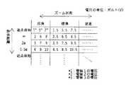
この電子撮像装置301は、コントラスト方式のオートフォーカス機能を備えており、可変ミラー409は次のように駆動される。マイクロコンピュータ311は、ルックアップテーブル300を参照しつつ、可変ミラー駆動回路310を介して可変ミラー409の電極409bに異なる電圧を加えて反射膜409aを変形させ、予め何枚かの画像を撮像する。そして、固体撮像素子408から電子回路312を介して入力されたそれらの画像情報の中から高周波成分を取り出し、ルックアップテーブル300の参照あるいはルックアップテーブル300の中の数値の補間あるいは外挿によって、高周波成分が最大になる駆動電圧を算出する。そして、その算出された駆動電圧を可変ミラー409に印加して撮像が行なわれる。尚、マイクロコンピュータ311には、温度センサー415と湿度センサー416が接続されている。
【0012】
このとき、参照するルックアップテーブル300の一例が図2に示されている。このように、ルックアップテーブル300は、縦軸,横軸の一方を物体距離、他方をズーム状態としたものであればよい。また、ズーム状態は、例えばズームモータ307Dに送られるパルス数によって検出され、ズーム状態に対応した部分、即ち物体距離を変えた数値によって、可変ミラー409に加わる電圧を変えればよい。このほか、ズーム状態は、変倍レンズ306の位置を検出するエンコーダで検出するようにしてもよい。
【0013】
このようにして、固体撮像素子408で撮像した画像は、電子回路312で処理され、記憶装置313に記憶される。また、表示装置314に表示させることもできる。その場合、表示装置314としては、CRTディスプレイであっても差し支えないが、通常の液晶ディスプレイ,反射・透過兼用のディスプレイ,反射型液晶ディスプレイ,有機ELディスプレイ等の方が、消費電力が少ないので好ましい。
【0014】
このような本実施例において、可変ミラー409と可変ミラー駆動回路310で消費される電力は、通常にフォーカシング用レンズをモータで駆動する場合(0.3〜5W程度)に比べて、数分の1〜数十分の1(数十mW〜200mW)と小さい。従って、ズームモータ駆動時(このとき、ズームモータ307D,ズームモータ駆動回路307Eで0.3〜5Wの電力を消費する)でも、可変ミラー409によってオートフォーカスを行なうことが可能になり、ビデオカメラあるいはデジタルカメラ等での動画撮影時に、ズーミングをしているときでも常にピントの合った動画が撮影できることになる。
【0015】
また、このメリットは、ビデオカメラやデジタルカメラの場合には勿論であるが、図1に示した光学系を、テレビカメラや映画用フィルムカメラ等に用いた場合にも得られる。但し、映画用フィルムカメラに用いる場合は、図1における固体撮像素子408が、フィルムに置き換わることになる。
【0016】
本実施例におけるズームの制御についてのフローチャートを図3(a)に示し、オートフォーカスの制御についてのフローチャートを図3(b)に示した。また、本実施例は、動画撮影に限らず、静止画撮影をする場合でも、オートフォーカスを行ないつつズーミングを行なって、良いフレーミングになったときにシャッターを押せば、オートフォーカスのタイムラグがなく、ピントの合った画像が得られる。
【0017】
[実施例2]
図1には、本実施例の構成に必要な音声集録用のマイクロフォン325と、マイクロフォン制御回路325Bが示されている。そして、このように構成すると、動画,静止画の撮影中に音声の集録ができ、記憶装置313に記録することが可能になる。即ち、従来のように、フォーカシング用レンズをモータで駆動する場合には、ズルズルという騒音やジーッという騒音が出るため、オートフォーカスを行ないつつ録音することはできなかったが、本実施例の場合には、可変ミラー409の動作時に騒音を発生しないため、オートフォーカスを行ないつつ録音することが可能になる。図4に、動画撮影時のフローチャートを示した。
【0018】
[実施例3]
図1において、表示装置314がオンになっているときには、表示装置314には、固体撮像素子408で撮像された画像が表示されている。そのため、例えば、静止画像を撮影するときのファインダーのように、撮影時以外でも動画を表示し続けているようにすることができる。ところが、従来は、このような表示装置314の使い方をしたとき、オートフォーカスを常時行なっているようにすることができなかった。なぜなら、オートフォーカス用のモータの消費電力が大きく、電池の消耗が激しかったからである。
【0019】
ところが、図1に示した電子撮像装置301の場合は、可変ミラー409の消費電力が少ないため、表示装置314を使用しているときにも、常時、オートフォーカスを行なうことが可能となる。そのため、被写界中の物体距離が変わっても、表示装置314には、常にピントの合った画像が表示されることになる。また、上記した特願2001−37454号の図1に示された実施例には、光学式ファインダーが設けられているが、表示装置314に、常にピントの合った画像が表示されることによって、そのような光学式ファインダーを設ける必要がなくなるとともに、撮像装置が小型・軽量になるというメリットもある。図5には、そのように構成した場合のフローチャートを示してある。
【0020】
尚、さらに消費電力を減らすためには、表示装置314の使用時に常にオートフォーカスを行なわせず、可変ミラー409に対して、常に遠方の距離(例えば70cm、あるいは1m以上)にピントが合うように、電圧を印加しておくようにすればよい。そうすれば、殆どの使用状態では表示装置314にボケのない画像が表示でき便利である。また、可変ミラー409に印加する電圧をオフにしても差し支えない。その場合には、撮影系のピントは、∞又はその近傍に合うようになるので、殆どの使用状態では表示装置314にボケの少ない画像が表示され、実用に供せるものとなる。また、消費電力を減らすために、表示装置314がオフにされ、かつオートフォーカスを行なっていない場合には、可変ミラーへの通電を行なわないようにすると良い。
【0021】
[実施例4]
また、実施例1と実施例3で説明したように、可変ミラー409を用いると、消費電力が減るので、予備の電池を持ち歩かなくてもよくなるというメリットがある。そこで、本実施例の場合は、図1に示されているように、電源回路340用の電源に、充電式電池330を用いる。そして、その電池330を電子撮像装置301のボディー内に埋め込み、接点331だけをボディーの外面に出すことによって、充電器332で随時充電して使うようにしている。このようにしたことによって、電池交換のための機械的部材(電池のフタ、ケース等)が不要になり、電子撮像装置301の小型・軽量化が可能になる。また、接点331をボディー外面に設けず、電磁誘導により充電器と非接触で電池330を充電できるようにしてもよく、そのようにすると、接点331がなくなるので、一層好適なものになる。
【0022】
[実施例5]
本実施例は、図1に示されている可変ミラー駆動回路310を工夫することによって、特殊な機能が得られるようにしたものである。図6は、可変ミラー409を、時間的に変化する電気で駆動するようにした例を示したものである。そのため、図1に示された可変ミラー駆動回路310に代わって可変ミラー駆動回路333が用いられる。この可変ミラー駆動回路333は、AC駆動回路333AとDC駆動回路333Bとを内蔵しており、これまで説明したような撮影時におけるオートフォーカス用には、DC駆動回路333Bが用いられる。
【0023】
他方、AC駆動回路333Aを用いて可変ミラー409を駆動する場合、周波数fが可聴周波数(20〜20kHz)内であって、例えば、f=880Hz,440Hz,2kHzなどにすると、3層の変形膜(409a,409j,409k)は振動し、音を発生する。そこで、本実施例の場合には、このスピーカー機能を有効に活用することにする。例えば、電子撮像装置301がデジタルカメラの場合には、デジタルカメラの各種警告音の発生源として使うことができる。また、電子撮像装置301が携帯電話に内蔵された撮像装置の場合には、受話器のスピーカとして使え、電話の音声伝達,着メロの発生などに使うことができる。
【0024】
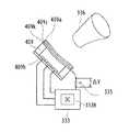
また、図7に示したように、可変ミラー駆動回路333として、周波数fpのパルス幅変調(PWM)方式の駆動回路333cを用いると、周波数fpを可聴帯域内に選ぶことによって、可変ミラー409をスピーカとして使用することができる。また、周波数fpを可変ミラー409の変形膜の共振周波数fe以上の高周波(好ましくはfp≧10fe)に選べば、変形膜は殆ど振動しないので、可変ミラー409を撮影時のオートフォーカスに用いることが可能になる。図8は、パルス幅変調方式の駆動回路333cから出力される電圧の時間変化を示したもので、Vcの値は一定であり、電圧が0の時とVcのときとの時間比率を変えることで、実効的に可変ミラー409に加わる電圧を変化させるようにする。周期Τ=1/fpの関係がある。尚、本実施例の場合、可変ミラー409の近傍であって光学系の光路外にホーン334を設けておけば、可変ミラー409の発する音が増幅されて好適になる。
【0025】
[実施例6]
本実施例は、図9に示されているように、可変ミラー409を、音の集録用のマイクロフォンとしても使用した例である。可変ミラー409の二つの電極409k,409b間には直流電圧が加えられており、音波によって、3層の変形膜(409a,409j,409k)が振動すると、可変ミラー409の静電容量が変化するので、電流が流れ、抵抗335の両端に電位差ΔVが生ずる。この電圧を増幅すれば、スピーカから音を出せるわけで、可変ミラー409は、マイクロフォンとして動作することになる。尚、可変ミラー409の電極間には、可聴帯域より高い周波数の交流電圧を加えてもよい。更に、集音用のホーン336を、可変ミラー409の近傍であって光学系の光路外に設ければ、マイクロフォンの能率を上げることが可能となる。
【0026】
[実施例7]
本実施例は、撮影時に、物体までの距離に応じて、光学系のモード切り替えをしないようにしたものである。図1に示された電子撮像装置301によれば、それが可能である。なぜならば、従来のように、モータを駆動源としたコントラスト方式のオートフォーカスを行なう場合には、レンズの移動量が大きいため、全ての距離に対して迅速にオートフォーカスを行なうことができず、例えば物体距離を、∞から70cmまで(通常)と、70cmから20cmまで(マクロ)との二つに分けて、使用者がどちらの距離に物体があるかを判断した上で、オートフォーカスのモードを選択し撮影していたが、可変ミラー409を用いれば、3層の変形膜の変形速度は数ms以下と速いので、全ての物体距離についてオートフォーカスが行なえるからである。従って、使用者によるマクロモードへの切り替えが不要になる。
【0027】
以上の実施例1〜7においては、光学特性可変光学素子として、面形状可変光学素子(面形状の変化するミラー,レンズ,プリズム等)の一つである可変ミラー409を用いていたが、本発明は、これに限るものではない。実施例1,2,4,7の場合には、可変ミラー409の代わりに、図10〜図20に示す可変焦点レンズや、図21に示す可変焦点ミラー等を用いても同等の効果を得ることができる。そこで、それらの可変焦点レンズや可変焦点ミラー等を、以下に説明する。
【0028】
図10は可変焦点レンズの原理的構成を示す図である。この可変焦点レンズ511は、第1.第2の面としてのレンズ面508a,508bを有する第1のレンズ512aと、第3,第4の面としてのレンズ面509a,509bを有する第2のレンズ512bと、これらレンズ間に透明電極513a,513bを介して設けた高分子分散液晶層514とを有し、入射光を第1,第2のレンズ512a,512bを経て収束させるものである。透明電極513a,523bは、スイッチ515を介して交流電源516に接続して、高分子分散液晶層514に交流電界を選択的に印加するようにする。尚、高分子分散液晶層514は、それぞれ液晶分子517を含む球状、多面体等の任意の形状の多数の微小な高分子セル518を有して構成し、その体積は、高分子セル518を構成する高分子及び液晶分子517がそれぞれ占める体積の和に一致させる。
【0029】
ここで、高分子セル518の大きさは、例えば球状とする場合、使用する光の波長をλとしたとき、その平均の直径Dを、例えば、
2nm≦D≦λ/5 ・・・(1)
とする。即ち、液晶分子517の大きさは、2nm程度以上であるので、平均の直径Dの下限値は、2nm以上とする。また、Dの上限値は、可変焦点レンズ511の光軸方向における高分子分散液晶層514の厚さtにも依存するが、λに比べて大きいと、高分子の屈折率と液晶分子517の屈折率との差により、高分子セル518の境界面で光が散乱して高分子分散液晶層514が不透明になってしまうため、好ましくはλ/5以下とする。可変焦点レンズが用いられる光学製品によっては高精度を要求しない場合もあり、そのときにはDはλ以下でも良い。尚、高分子分散液晶層514の透明度は、厚さtが厚いほど悪くなる。
【0030】
ここで、図10に示すように、スイッチ515をオフ、即ち高分子分散液晶514に電界を印加しない状態では、液晶分子517が様々な方向を向いているので、入射光に対する高分子分散液晶層514の屈折率は高く、屈折力の強いレンズとなる。これに対し、図11に示すように、スイッチ515をオンとして高分子分散液晶層514に交流電界を印加すると、液晶分子517は、屈折率楕円体の長軸方向が可変焦点レンズ511の光軸と平行となるように配向するので、屈折率が低くなり、屈折力の弱いレンズとなる。
【0031】
図12は可変焦点回折光学素子の一例の構成を示す図である。この可変焦点回折光学素子531は、平行な第1,第2の面532a,532bを有する第1の透明基板532と、光の波長オーダーの溝深さを有する断面鋸歯状のリング状回折格子を形成した第3の面533a及び平坦な第4の面533bを有する第2の透明基板533とを有し、入射光を第1,第2の透明基板532,533を経て出射させるものである。第1,第2の透明基板532,533間には、透明電極513a,513bを介して高分子分散液晶層514を設け、透明電極513a,513bをスイッチ515を経て交流電源516に接続して、高分子分散液晶層514に交流電界を印加するようにする。
【0032】
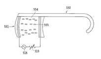
図13及び図14は、可変焦点眼鏡550の構成を示すものであり、可変焦点レンズ551は、レンズ552及び553と、これらレンズの内面上にそれぞれ透明電極513a,513bを介して設けた配向膜539a,539bと、これらは以降膜間に設けたツイストネマティック液晶層554とを有して構成し、その透明電極513a,513bを可変抵抗器519を経て交流電源516に接続して、ツイストネマティック液晶層554に交流電界を印加するようにする。かかる構成において、ツイストネマティック液晶層554に印加する電圧を高くすると、液晶分子555は、図14に示すようにホメオトロピック配向となり、図13に示す印加電圧が低いツイストネマティック状態の場合に比べて、ツイストネマティック液晶層554の屈折率は小さくなり、焦点距離が長くなる。
【0033】
図15は、可変焦点レンズ140を用いた撮像ユニット141の概略構成図である。撮像ユニット141は本発明の撮像系として用いることができる。本例では、レンズ102と可変焦点レンズ140とで、撮像レンズを構成している。そして、この撮像レンズと固体撮像素子408とで撮像ユニット141を構成している。可変焦点レンズ140は、透明部材142と圧電性のある合成樹脂等の柔らかい透明物質143とで、光を透過する流体あるいはゼリー状物質144を挟んで構成されている。
【0034】
流体あるいはゼリー状物質144としては、シリコンオイル,弾性ゴム,ゼリー,水等を用いることができる。透明物質143の両面には透明電極145が設けられており、回路103を介して電圧を加えることで、透明物質143の圧電効果により透明物質143が変形し、可変焦点レンズ140の焦点距離が変わるようになっている。従って、本例によれば、物体距離が変わった場合でも光学系をモータ等で動かすことなくフォーカスができ、小型、軽量、消費電力が少ない点で優れている。
【0035】
図16は圧電材料200を用いた可変焦点レンズ201の概略構成図である。圧電材料200には透明物質143と同様の材料が用いられており、圧電材料200は、透明で柔らかい基板202の上に設けられている。尚、基板202には、合成樹脂、有機材料を用いるのが望ましい。このような本例においては、2つの透明電極59を介して電圧を圧電材料200に加えることで圧電材料200は変形し、図16において凸レンズとしての作用を持っている。
【0036】
尚、基板202の形をあらかじめ凸状に形成しておき、かつ、2つの透明電極59のうち、少なくとも一方の電極の大きさを基板202と異ならせておく、例えば、一方の透明電極59を基板202より小さくしておくと、電圧を切ったときに、図17に示すように、2つの透明電極59が対向する所定部分だけが凹状に変形して凹レンズの作用を持つようになり、可変焦点レンズとして動作する。このとき、基板202は、流体161の体積が変化しないように変化するので、液溜168が不要になるというメリットがある。
【0037】
図18は圧電材料からなる2枚の薄板200A,200Bを用いた可変焦点レンズの概略構成図である。本例の可変焦点レンズは、薄板2000Aと200Bの材料の方向性を反転させることで、変形量を大きくし、大きな可変焦点範囲が得られるというメリットがある。尚、図18中、204はレンズ形状の透明基板である。
【0038】
図19は可変焦点レンズの例を示す概略構成図である。本例の可変焦点レンズ207は、例えばシリコンゴムやアクリルエラストマー等の電歪材料206を用いて構成されている。本例の構成によれば、電圧が低いときには、図19に示すように、凸レンズとして作用し、電圧を上げると、図20に示すように、電歪材料206が上下方向に伸びて左右方向に縮むので、焦点距離が伸びる。従って、可変焦点レンズとして動作する。このような本例の可変焦点レンズによれば、大電源を必要としないので、消費電力が小さくて済むというメリットがある。
【0039】
図21は可変焦点レンズを用いた可変焦点ミラーを示すものである。この可変焦点ミラー565は、第1,第2の面566a,566bを有する第1の透明基板566と、第3,第4の面567a,567bを有する第2の透明基板567とを有する。第1の透明基板566は、平板状又はレンズ状に形成して、内面(第2の面)566bに透明電極513aを設け、第2の透明基板567は、内面(第3の面)567aを凹面状に形成して、該凹面上に反射膜568を施し、さらにこの反射膜568上に透明電極513bを設ける。透明電極513a,513b間には、高分子分散液晶層514を設け、これら透明電極513a,513bをスイッチ515及び可変抵抗器519を経て交流電源516に接続して、高分子分散液晶層514に交流電界を印加するようにする。尚、図21では、液晶分子の図示を省略してある。
【0040】
かかる構成によれば、透明基板566側から入射する光線は、反射膜568により高分子分散液晶層514を折り返す光路となるので、高分子分散液晶層514の作用を2回もたせることができると共に、高分子分散液晶層514への印加電圧を変えることにより、反射光の焦点位置を変えることができる。尚、透明基板566又は567の内面を、図12に示したように回折格子状にして、高分子分散液晶層514の厚さを薄くすることもできる。このようにすれば、散乱光をより少なくできる利点がある。
【0041】
また、上記の実施例1,2,3,4,7は、図22〜図24に示す光学装置に適用しても、その効果を発揮することができる。そこで、それらの光学装置を以下に説明する。
【0042】
図22は、光学特性可変ミラーを用いたデジタルカメラのケプラー式ファインダーの概略構成図である。本例の構成は、もちろん、銀塩フィルムカメラにも使うことができる。物体からの光は、対物レンズ902及びプリズム404の各入射面と射出面で屈折され、可変形状鏡409で反射され、プリズム404を透過して、二等辺直角プリズム405でさらに反射され(図22中、光路中の+印は、紙面の裏側へ向かって光線が進むことを示している。)、ミラー406で反射され、接眼レンズ901を介して眼に入射するようになっている。このように、レンズ901,902、プリズム404,405、及び、可変形状鏡409によって、本例の光学装置の観察光学系を構成しており、これらの各光学素子の面形状と肉厚を最適化することにより、物体面の収差を最小にすることができるようになっている。
【0043】
即ち、反射面としての薄膜409aの形状は、結像性能が最適になるように演算装置414からの信号により各可変抵抗器411の抵抗値を変化させることにより制御される。即ち、演算装置414へ、温度センサー415、湿度センサー416及び距離センサー417から、周囲温度及び湿度並びに物体までの距離に応じた大きさの信号が入力され、演算装置414は、これらの入力信号に基づき周囲の温度及び湿度条件と物体までの距離による結像性能の低下を補償すべく、薄膜409aの形状が決定されるような電圧を電極409bに印加するように、可変抵抗器411の抵抗値を決定するための信号を出力する。このように、薄膜409aは電極409bに印加される電圧すなわち静電気力で変形させられるため、その形状は状況により非球面を含む様々な形状をとり、印加される電圧の極性を変えれば凸面とすることもできる。尚、距離センサー417はなくてもよく、その場合、固体撮像素子408からの像の信号の高周波成分が略最大になるように、デジタルカメラの撮像レンズ403を動かし、その位置から逆に物体距離を算出し、可変形状鏡を変形させて観察者の眼にピントが合うようにすればよい。
【0044】
図23は、可変形状鏡409を用いた撮像系、例えば携帯電話のデジタルカメラ、カプセル内視鏡、電子内視鏡、パソコン用デジタルカメラ、PDA用デジタルカメラ等に用いられる撮像系の概略構成図である。本例の撮像系は、可変形状鏡409と、レンズ902と、固体撮像素子408と、制御系103とで一つの撮像ユニット104を構成している。本例の撮像ユニット104では、レンズ102を通った物体からの光は可変形状鏡409で集光され、固体撮像素子408の上に結像する。可変形状鏡409は、光学特性可変光学素子の一種であり、可変焦点ミラーとも呼ばれている。
【0045】
本例によれば、物体距離が変わっても可変形状鏡409を変形させることでピント合わせをすることができ、レンズをモータ等で駆動する必要がなく、小型化、軽量化、低消費電力化の点で優れている。また、可変形状鏡409を複数用いることでズーム、変倍の撮像系、光学系を作ることができる。尚、図23では、制御系103にコイルを用いたトランスの昇圧回路を含む制御系の構成例を示している。特に積層型圧電トランスを用いると、小型化できてよい。昇圧回路は、特に静電気力、圧電効果を用いる場合の可変形状鏡、可変焦点レンズに有用である。
【0046】
図24は、デジタルカメラ用の撮像光学系の構成を示すものである。この撮像光学系においては、物体(図示せず)の像を、絞り521、可変焦点レンズ511及びレンズ522を介して、例えばCCDよりなる固体撮像素子523上に結像させる。尚、図24では、液晶分子の図示を省略してある。かかる撮像光学系によれば、可変抵抗器519により可変焦点レンズ511の高分子分散液晶層514に印加する交流電圧を調整して、可変焦点レンズ511の焦点距離を変えることにより、可変焦点レンズ511及びレンズ522を光軸方向に移動させることなく、例えば、無限遠から600mmまでの物体距離に対して、連続的に合焦させることが可能となる。
【0047】
また、上記の実施例1,2,3,4,7における可変ミラーとしては、図27に示すような、圧電効果を有する材料等で駆動するもの、あるいは図28に示す電磁力で駆動するものを用いてもよい。そこで、それらについて説明する。
【0048】
先ず、図27は、圧電効果を有する材料で駆動する可変形状鏡409の例を示す概略構成図である。本例の可変形状鏡は、薄膜409aと電極409bとの間に圧電素子409cが介装されていて、これらが支持台423上に設けられている。そして、圧電素子409cに加わる電圧を各電極409b毎に変えることにより、圧電素子409cに部分的に異なる伸縮を生じさせて、薄膜409aの形状を変えることができるようになっている。電極409bの形は、同心分割であってもよいし、矩形分割であってもよく、その他、適宜の形のものを選択することができる。
【0049】
図27中、符号424は演算装置414に接続された振れ(ブレ)センサーであって、例えばデジタルカメラの振れを検知し、振れによる像の乱れを補償するように薄膜409aを変形させるべく、演算装置414及び可変抵抗器411を介して電極409bに印加される電圧を変化させる。このとき、温度センサー415、湿度センサー416及び距離センサー417からの信号も同時に考慮され、ピント合わせ、温・湿度補償等が行なわれる。この場合、薄膜409aには圧電素子409cの変形に伴う応力が加わるので、薄膜409aの厚さはある程度厚めに作られて相応の強度を持たせるようにするのがよい。
【0050】
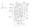
次に、図28は、電磁力で駆動する可変形状鏡409の例を示す概略構成図である。本例の可変形状鏡は、電磁気力を利用して反射面の形状を変化させ得るようにしたもので、支持台423の内部底面上には永久磁石426が、頂面上には窒化シリコン又はポリイミド等からなる基板409eの周縁部が載置固定されており、基板409eの表面にはアルミニウム等の金属コートで作られた薄膜409aが付設されていて、可変形状鏡409を構成している。基板409eの下面には複数のコイル427が配設されており、これらのコイル427はそれぞれ駆動回路428を介して演算装置414に接続されている。
【0051】
従って、各センサー415,416,417,424からの信号によって演算装置414において求められている光学系の変化に対応した演算装置414からの出力信号により、各駆動回路428から各コイル427にそれぞれ適当な電流が供給されると、永久磁石との間に働く電磁気力で各コイル427は反発又は吸着され、基板409e及び薄膜409aを変形させる。この場合、各コイル427はそれぞれ異なる量の電流を流すようにすることもできる。また、コイル427は1個でもよいし、永久磁石426を基板409eに付設しコイル427を支持台423の内部底面側に設けるようにしてもよい。また、コイル427はリソグラフィー等の手法で作るとよく、さらに、コイル427には強磁性体よりなる鉄心を入れるようにしてもよい。
【0052】
また、上記の実施例5,6の場合に、可変ミラー409の代わりに用いることのできる光学特性可変光学素子は、上記の面形状可変光学素子である必要がある。そして、その面形状可変光学素子としては、図15〜図20に示されたもののほかに、図25,図26に示す可変焦点レンズ等があり、それらを可変ミラー409の代わりに用いても、実施例5,6の場合と同様な効果を得ることができる。そこで、それらの可変焦点レンズについて説明する。
【0053】
図25は、図15の例において、シリンダー146を設ける代わりに、支援部材147を設けてシリンダー146を省略した構造にした例である。支援部材147は、間に透明電極145を挟んで、透明物質143の一部の周辺部分を固定している。本例によれば、透明物質143に電圧をかけることによって、透明物質143が変形しても、可変焦点レンズ140全体の体積が変わらないように変形するため、シリンダー146が不要になる。尚、図25中、符号148は変形可能な部材で、弾性体、アコーディオン状の合成樹脂または金属等でできている。
【0054】
また、図26は、マイクロポンプ160で流体161を出し入れし、レンズ面を変形させる可変焦点レンズ162の概略構成図である。マイクロポンプ160は、例えば、マイクロマシンの技術で作られた小型のポンプで、電力で動くように構成されている。流体161は、透明基板163と、弾性体164との間に挟まれている。図26中、符号165は弾性体164を保護するための透明基板であるが、設けなくてもよい。マイクロマシンの技術で作られたポンプの例としては、熱変形を利用したもの、圧電材料を用いたもの、静電気力を用いたものなどがある。
【0055】
尚、上記の実施例の光学装置では、電源として、充電式電池を用いた場合で説明したが、使い捨ての乾電池を用いてもよい。また、電池と商用電源(AC100V,200V等)とを併用できるようにしてもよい。
【0056】
以上説明したように、本発明は、特許請求の範囲に記載した特徴のほかに下記の特徴を有している。
【0057】
(1)動画撮影時にオートフォーカスとズームとを同時に行なうことを特徴とする請求項1に記載の光学装置。
(2)オートフォーカスとズームとを同時に行ないつつ静止画を撮影することができることを特徴とする請求項1に記載の光学装置。
【0058】
(3)光学特性可変光学素子を備え、オートフォーカスを行ないつつ音声入り動画撮影を行なうことを特徴とする光学装置。
(4)光学特性可変光学素子を備え、オートフォーカスを行ないつつ音声入り静止画撮影を行なうことを特徴とする光学装置。
【0059】
(5)光学ファインダーを備えないことを特徴とする請求項3記載の光学装置。
(6)光学特性可変光学素子を備えており、表示装置に画像を表示しているときにオートフォーカスを行なわない場合には、無限遠あるいは遠方(たとえば1m以上)にピントが合うように前記光学特性可変光学素子が構成されていることを特徴とする光学装置。
【0060】
(7)充電式電池を備えており、前記充電式電池が光学装置のボディーと一体化されていることを特徴とする光学特性可変光学素子を備えた光学装置。
(8)充電式電池を備えており、前記充電式電池が光学装置のボディと一体化されていて、充電用の接点をボディ外面に有することを特徴とする光学装置。
【0061】
(9)充電式電池を備えており、前記充電式電池が光学装置のボディと一体化されているが、充電用の接点をボディ外面に有しないことを特徴とする光学装置。
(10)電磁誘導によって前記充電式電池を充電することを特徴とする上記(9)に記載の光学装置。
【0062】
(11)充電式電池を備えており、前記充電式電池の交換がユーザにはできないことを特徴とする光学特性可変光学素子を備えた光学装置。
(12)形状可変光学素子を時間的に変化する電気で駆動し、前記光学素子面を振動させることで、音を出すことを特徴とする、形状可変光学素子とその駆動回路。
【0063】
(13)光学系の邪魔にならない位置にホーンを設けたことを特徴とする上記(12)に記載の形状可変光学素子とその駆動回路。
(14)形状可変光学素子を周波数fの時間的に変化する電気で駆動し、かつf>feであり、前記光学素子面を振動させることで、音を出すことを特徴とする、形状可変光学素子とその駆動回路。
但し、feは形状可変光学素子の変形する部材の共振周波数である。
【0064】
(15)前記形状可変光学素子をPWM駆動回路で駆動することを特徴とする上記(12)〜(14)の何れかに記載の、形状可変光学素子とその駆動回路。
(16)ホーンを備えたことを特徴とする上記(12),(14),(15)の何れかに記載の形状可変光学素子とその駆動回路。
【0065】
(17)変形可能な電極を備えた形状可変光学素子において、電極間に電圧を加え、前記変形可能な電極が音波で振動する際の静電容量の変化を電気的に検出することでマイクロフォンの機能を持たせたことを特徴とする形状可変光学素子。
(18)変形可能な電極を備えた形状可変光学素子において、電極間に直流電流を加え、前記変形可能な電極が音波で振動する際の静電容量の変化を電気的に検出することでマイクロフォンの機能を持たせたことを特徴とする形状可変光学素子。
【0066】
(19)変形可能な電極を備えた形状可変光学素子において、電極間に交流電流を加え、前記変形可能な電極が音波で振動する際の静電容量の変化を電気的に検出することでマイクロフォンの機能を持たせたことを特徴とする形状可変光学素子。
(20)ホーンを備えたことを特徴とする上記(17)〜(19)の何れかに記載の形状可変光学素子。
【0067】
(21)光学特性可変光学素子を備え、被写体の距離によってマクロモード切り替えを行なわずに撮影ができることを特徴とする光学装置。
(22)光学特性可変光学素子が可変ミラーであることを特徴とする請求項1,2,3、上記(1)〜(21)の何れかに記載の光学装置。
【0068】
(23)光学特性可変光学素子が可変焦点レンズであることを特徴とする請求項1,2,3、上記(1)〜(21)の何れかに記載の光学装置。
(24)電源が電池であることを特徴とする請求項1,2,3、上記(1)〜(21)の何れかに記載の光学装置。
【0069】
(25)電源が充電式の電池であることを特徴とする請求項1,2,3、上記(1)〜(21)の何れかに記載の光学装置。
(26)形状可変光学素子が、可変ミラーであることを特徴とする上記(12)〜(21)の何れかに記載の光学装置。
【0070】
(27)形状可変光学素子が、可変焦点レンズであることを特徴とする上記(12)〜(21)の何れかに記載の光学装置。
(28)周期的に変化する電圧または電流で、光学特性可変光学素子または形状可変光学素子を駆動することを特徴とする請求項1,2,3、上記(12)〜(26)の何れかに記載の光学装置。
【0071】
【発明の効果】
以上の説明から明らかなように、本発明によれば、消費電力が少ない、小型で軽量な光学装置が得られる。
【図面の簡単な説明】
【図1】一部他の実施例の構成も含めた実施例1の構成説明図である。
【図2】図1に示されているルックアップテーブルの具体的な一例を示した図である。
【図3】図3(a)は実施例1におけるズームの制御についてのフローチャートであり、図3(b)は実施例1におけるオートフォーカスの制御についてのフローチャートである。
【図4】実施例2の動画撮影時における制御例を示したフローチャートである。
【図5】実施例3の制御例を示したフローチャートである。
【図6】実施例5の構成を説明するための図である。
【図7】実施例5の変形例の構成を説明するための図である。
【図8】図7に示した変形例の電気的駆動方式を説明するための図である。
【図9】実施例6の構成を説明するための図である。
【図10】可変焦点レンズの原理的構成を示す図である。
【図11】図10に示す高分子分散液晶層に電界を印加した状態を示す図である。
【図12】可変焦点回折光学素子の一例の構成を示す図である。
【図13】ツイストネマティック液晶を用いる可変焦点レンズを有する可変焦点眼鏡の構成を示す図である。
【図14】図13に示すツイストネマティック液晶層への印加電圧を高くしたときの液晶分子の配向状態を示す図である。
【図15】可変焦点レンズ140を用いた撮像ユニット141の概略構成図である。
【図16】圧電材料200を用いた可変焦点レンズ201の概略構成図である。
【図17】図16の変形例に係る可変焦点レンズの状態説明図である。
【図18】圧電材料からなる2枚の薄板200A,200Bを用いた可変焦点レンズの概略構成図である。
【図19】可変焦点レンズの例を示す概略構成図である。
【図20】図19の例に係る可変焦点レンズの状態説明図である。
【図21】可変焦点レンズとしての可変焦点ミラーの一例の構成を示す図である。
【図22】光学装置の一例に係る光学特性ミラーを用いたデジタルカメラのケプラー式ファインダーの概略構成図である。
【図23】可変形状鏡409を用いた撮像系、例えば携帯電話のデジタルカメラ、カプセル内視鏡、電子内視鏡、パソコン用デジタルカメラ、PDA用デジタルカメラ等に用いられる撮像系の概略構成図である。
【図24】可変焦点レンズを用いたデジタルカメラ用の撮像光学系の一例の構成を示す図である。
【図25】図15の例における可変焦点レンズの変形例を示す説明図である。
【図26】マイクロポンプ160で流体161を出し入れし、レンズ面を変形させる可変焦点レンズ162の概略構成図である。
【図27】圧電効果を有する材料で駆動する可変形状鏡409の例を示す概略構成図である。
【図28】電磁力で駆動する可変形状鏡409の例を示す概略構成図である。
【符号の説明】
300 ルックアップテーブル
301 電子撮像装置
302 プラスチックレンズ
303,304 プラスチックレンズ枠
306 変倍レンズ
307A カム板
307B,307C カムピン
307D ズームモータ
307E ズームモータ駆動回路
310,333 可変ミラー駆動回路
311 マイクロコンピュータ
312 電子回路
313 記憶装置
314 表示装置
315,319 凹レンズ
316,317 凸レンズ
318 非球面レンズ
320 物体
321 絞り
325 マイクロフォン
325B マイクロフォン制御回路
330 充電式電池
331 接点
332 充電器
333A AC駆動回路
333B DC駆動回路
333C パルス幅変調方式の駆動回路
334,336 ホーン
335 抵抗
340 電源回路
408 固体撮像素子
409 可変ミラー
409a 反射膜
409b,409k 電極
409j 基板
415 温度センサ
416 湿度センサ[0001]
TECHNICAL FIELD OF THE INVENTION
The present invention relates to an optical device provided with an optical characteristic variable optical element.
[0002]
[Prior art]
For example, some optical devices such as digital cameras, video cameras, microscopes, and electronic endoscopes have an autofocus function. In a normal case, the focusing is performed by moving the lens along the optical axis by a motor. On the other hand, Japanese Unexamined Patent Publication No. 2000-267010 discloses a variable mirror having a special configuration different from conventional glass or plastic optical parts and having optical characteristics changed by electrical control. , Variable-focus lenses, variable prisms and other optical characteristics variable optical elements are disclosed. The present invention relates to an optical device provided with such an optical characteristic variable optical element.
[0003]
[Problems to be solved by the invention]
In the case of performing autofocus in an optical device such as a digital camera, a motor has been used as a drive source and a lens is moved via a mechanical drive mechanism as described above. Such an autofocus mechanism has drawbacks such as the motor and drive mechanism generating noise, high power consumption, and large dimensions and weight of the entire mechanism. For this reason, since noise is generated and power consumption is large, other functions required for the optical device cannot be performed in parallel during focusing, or it can be performed. Therefore, there was a problem that special measures were required. In addition, since a motor and a driving mechanism are required to move the focusing lens, there is a problem that the optical device is inevitably increased in size.
[0004]
The present invention has been made in order to solve such a problem, and an object of the present invention is to provide an optical characteristic variable optical element such as a variable mirror or a variable focus lens described above, for Another object of the present invention is to provide a small-sized and light-weight optical device which has low power consumption and enables other functions to work properly in parallel.
[0005]
[Means for Solving the Problems]
In order to achieve the above object, an optical device of the present invention includes an optical characteristic variable optical element, and performs autofocus and zoom simultaneously. Further, the optical apparatus of the present invention is provided with an optical characteristic variable optical element, and performs photographing with sound while performing autofocus. Further, the optical device of the present invention is provided with an optical element having variable optical characteristics, and performs auto-focusing when an image is displayed on the display device.
[0006]
BEST MODE FOR CARRYING OUT THE INVENTION
Embodiments of the present invention will be described with reference to a plurality of examples. FIGS. 1 to 9 are used for describing the embodiments. 1 and 2 are basically for explaining the first embodiment, in which a configuration common to the other embodiments is shown, and FIG. , Specific items for other embodiments are also shown. Therefore, FIG. 1 is applied to embodiments other than the first embodiment.
[0007]
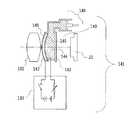
[Example 1]
The
[0008]
The configuration of the
[0009]
A
[0010]
The zooming mechanism includes a cam pin 307C provided on the
[0011]
The
[0012]
At this time, an example of the lookup table 300 to be referred to is shown in FIG. As described above, the lookup table 300 may be any table as long as one of the vertical axis and the horizontal axis is the object distance and the other is the zoom state. Further, the zoom state is detected by, for example, the number of pulses sent to the
[0013]
In this way, the image captured by the solid-
[0014]
In this embodiment, the electric power consumed by the
[0015]
This advantage can be obtained not only in the case of a video camera or a digital camera but also in the case where the optical system shown in FIG. 1 is used for a television camera, a movie film camera, or the like. However, when used for a movie film camera, the solid-
[0016]
FIG. 3A is a flowchart illustrating zoom control according to the present embodiment, and FIG. 3B is a flowchart illustrating autofocus control. In addition, the present embodiment is not limited to video shooting, even when shooting a still image, performing zooming while performing autofocus, if the shutter is pressed when good framing, there is no time lag of autofocus, An in-focus image is obtained.
[0017]
[Example 2]
FIG. 1 shows a
[0018]
[Example 3]
In FIG. 1, when the
[0019]
However, in the case of the
[0020]
In order to further reduce the power consumption, autofocus is not always performed when the
[0021]
[Example 4]
In addition, as described in the first and third embodiments, the use of the
[0022]
[Example 5]
In this embodiment, a special function is obtained by devising the variable
[0023]
On the other hand, when the
[0024]
Also, as shown in FIG. 7, the variable
[0025]
[Example 6]
In the present embodiment, as shown in FIG. 9, the
[0026]
[Example 7]
In this embodiment, the mode of the optical system is not switched according to the distance to the object at the time of shooting. According to the
[0027]
In the above-described first to seventh embodiments, the
[0028]
FIG. 10 is a diagram showing the basic configuration of a variable focus lens. This
[0029]
Here, when the size of the
2 nm ≦ D ≦ λ / 5 (1)
And That is, since the size of the
[0030]
Here, as shown in FIG. 10, when the
[0031]
FIG. 12 is a diagram showing a configuration of an example of a variable focus diffractive optical element. The variable focus diffractive
[0032]
13 and 14 show the configuration of the variable-
[0033]
FIG. 15 is a schematic configuration diagram of an
[0034]
As the fluid or jelly-
[0035]
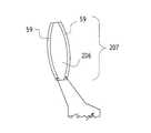
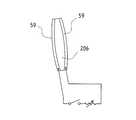
FIG. 16 is a schematic configuration diagram of a
[0036]
Note that the shape of the
[0037]
FIG. 18 is a schematic configuration diagram of a variable focus lens using two
[0038]
FIG. 19 is a schematic configuration diagram illustrating an example of a variable focus lens. The
[0039]
FIG. 21 shows a variable focus mirror using a variable focus lens. The
[0040]
According to such a configuration, a light ray incident from the
[0041]
Further, even when the above-described
[0042]
FIG. 22 is a schematic configuration diagram of a Kepler-type finder of a digital camera using a variable optical characteristic mirror. The configuration of this example can be used for a silver halide film camera. Light from the object is refracted at the entrance and exit surfaces of the
[0043]
That is, the shape of the
[0044]
FIG. 23 is a schematic configuration diagram of an imaging system using a
[0045]
According to this example, even if the object distance changes, focusing can be performed by deforming the
[0046]
FIG. 24 shows a configuration of an imaging optical system for a digital camera. In this imaging optical system, an image of an object (not shown) is formed on a solid-
[0047]
Further, as the variable mirror in the first, second, third, fourth and seventh embodiments, a mirror driven by a material having a piezoelectric effect as shown in FIG. 27 or a mirror driven by an electromagnetic force as shown in FIG. May be used. Therefore, they will be described.
[0048]
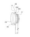
First, FIG. 27 is a schematic configuration diagram showing an example of a
[0049]
In FIG. 27,
[0050]
Next, FIG. 28 is a schematic configuration diagram showing an example of a
[0051]
Therefore, the output signals from the
[0052]
Further, in the case of the fifth and sixth embodiments, the optical characteristic variable optical element that can be used in place of the
[0053]
FIG. 25 is an example in which a
[0054]
FIG. 26 is a schematic configuration diagram of a varifocal lens 162 in which the
[0055]
In the optical device of the above embodiment, the description has been given of the case where a rechargeable battery is used as a power source. However, a disposable dry battery may be used. Further, a battery and a commercial power supply (AC100V, 200V, etc.) may be used in combination.
[0056]
As described above, the present invention has the following features in addition to the features described in the claims.
[0057]
(1) The optical device according to
(2) The optical device according to
[0058]
(3) An optical device comprising an optical element with variable optical characteristics, and capable of capturing a moving image with sound while performing autofocus.
(4) An optical device comprising an optical element with variable optical characteristics, and capable of capturing a still image with sound while performing autofocus.
[0059]
(5) The optical device according to (3), wherein no optical viewfinder is provided.
(6) The optical device is provided with an optical element with variable optical characteristics, and when auto-focusing is not performed when an image is displayed on a display device, the optical device is focused at infinity or at a distance (for example, 1 m or more). An optical device comprising a variable characteristic optical element.
[0060]
(7) An optical device having a variable optical characteristic optical element, comprising a rechargeable battery, wherein the rechargeable battery is integrated with a body of the optical device.
(8) An optical device comprising a rechargeable battery, wherein the rechargeable battery is integrated with the body of the optical device, and has a charging contact on the outer surface of the body.
[0061]
(9) An optical device comprising a rechargeable battery, wherein the rechargeable battery is integrated with the body of the optical device, but does not have a charging contact on the outer surface of the body.
(10) The optical device according to (9), wherein the rechargeable battery is charged by electromagnetic induction.
[0062]
(11) An optical device including an optical element with variable optical characteristics, wherein the optical device includes a rechargeable battery and the user cannot replace the rechargeable battery.
(12) A variable-shape optical element and a drive circuit thereof, wherein the variable-shape optical element is driven by time-varying electricity, and a sound is emitted by vibrating the optical element surface.
[0063]
(13) The variable shape optical element according to the above (12), wherein a horn is provided at a position that does not interfere with the optical system, and a driving circuit thereof.
(14) The shape-variable optical element is characterized in that the shape-variable optical element is driven by time-varying electricity having a frequency f, and f> fe, and a sound is emitted by vibrating the optical element surface. Element and its driving circuit.
Here, fe is the resonance frequency of the deformable member of the shape-variable optical element.
[0064]
(15) The variable shape optical element according to any one of the above (12) to (14), wherein the variable shape optical element is driven by a PWM drive circuit.
(16) The variable shape optical element according to any one of the above (12), (14) and (15), further comprising a horn, and a drive circuit therefor.
[0065]
(17) In the shape-variable optical element provided with a deformable electrode, a voltage is applied between the electrodes, and a change in capacitance when the deformable electrode vibrates with a sound wave is electrically detected, whereby the microphone is driven. A shape-variable optical element having a function.
(18) In a shape-variable optical element having a deformable electrode, a microphone is obtained by applying a direct current between the electrodes and electrically detecting a change in capacitance when the deformable electrode vibrates with a sound wave. A variable shape optical element characterized by having the function of (1).
[0066]
(19) In a shape-variable optical element having a deformable electrode, a microphone is applied by applying an alternating current between the electrodes and electrically detecting a change in capacitance when the deformable electrode vibrates with a sound wave. A variable shape optical element characterized by having the function of (1).
(20) The variable shape optical element according to any one of (17) to (19), further comprising a horn.
[0067]
(21) An optical device comprising an optical element with variable optical characteristics and capable of shooting without switching macro modes depending on the distance to the subject.
(22) The optical device according to any one of (1) to (21), wherein the optical characteristic variable optical element is a variable mirror.
[0068]
(23) The optical device according to any one of (1) to (21), wherein the optical characteristic variable optical element is a variable focus lens.
(24) The optical device according to any one of (1) to (21), wherein the power source is a battery.
[0069]
(25) The optical device according to any one of (1) to (21), wherein the power supply is a rechargeable battery.
(26) The optical device according to any one of (12) to (21), wherein the variable shape optical element is a variable mirror.
[0070]
(27) The optical device according to any one of (12) to (21), wherein the variable shape optical element is a variable focus lens.
(28) The optical characteristic variable optical element or the shape variable optical element is driven by a periodically changing voltage or current, and any one of the above (12) to (26). An optical device according to
[0071]
【The invention's effect】
As is clear from the above description, according to the present invention, a small and lightweight optical device with low power consumption can be obtained.
[Brief description of the drawings]
FIG. 1 is an explanatory diagram of a configuration of a first embodiment including a configuration of another embodiment.
FIG. 2 is a diagram showing a specific example of a look-up table shown in FIG. 1;
FIG. 3A is a flowchart illustrating zoom control according to the first embodiment, and FIG. 3B is a flowchart illustrating autofocus control according to the first embodiment.
FIG. 4 is a flowchart illustrating a control example at the time of capturing a moving image according to a second embodiment.
FIG. 5 is a flowchart illustrating a control example of a third embodiment.
FIG. 6 is a diagram for explaining a configuration of a fifth embodiment.
FIG. 7 is a diagram illustrating a configuration of a modification of the fifth embodiment.
FIG. 8 is a diagram for explaining an electric drive system according to the modification shown in FIG. 7;
FIG. 9 is a diagram for explaining a configuration of a sixth embodiment.
FIG. 10 is a diagram showing a basic configuration of a variable focus lens.
11 is a diagram showing a state where an electric field is applied to the polymer-dispersed liquid crystal layer shown in FIG.
FIG. 12 is a diagram showing a configuration of an example of a variable focus diffractive optical element.
FIG. 13 is a diagram showing a configuration of variable-focus glasses having a variable-focus lens using a twisted nematic liquid crystal.
FIG. 14 is a diagram showing an alignment state of liquid crystal molecules when a voltage applied to the twisted nematic liquid crystal layer shown in FIG. 13 is increased.
FIG. 15 is a schematic configuration diagram of an
FIG. 16 is a schematic configuration diagram of a
FIG. 17 is an explanatory diagram of a state of a variable focus lens according to a modification of FIG. 16;
FIG. 18 is a schematic configuration diagram of a variable focus lens using two
FIG. 19 is a schematic configuration diagram illustrating an example of a variable focus lens.
20 is an explanatory diagram of a state of the variable focus lens according to the example of FIG. 19;
FIG. 21 is a diagram illustrating a configuration of an example of a variable focus mirror as a variable focus lens.
FIG. 22 is a schematic configuration diagram of a Kepler-type finder of a digital camera using an optical characteristic mirror according to an example of an optical device.
FIG. 23 is a schematic configuration diagram of an imaging system using a
FIG. 24 is a diagram illustrating a configuration of an example of an imaging optical system for a digital camera using a variable focus lens.
FIG. 25 is an explanatory diagram showing a modification of the variable focus lens in the example of FIG.
FIG. 26 is a schematic configuration diagram of a varifocal lens 162 that deforms a lens surface by taking in and out a fluid 161 with a
FIG. 27 is a schematic configuration diagram showing an example of a
FIG. 28 is a schematic configuration diagram showing an example of a
[Explanation of symbols]
300 lookup table
301 Electronic imaging device
302 plastic lens
303, 304 plastic lens frame
306 Zoom lens
307A cam plate
307B, 307C Cam pin
307D zoom motor
307E zoom motor drive circuit
310,333 Variable mirror drive circuit
311 microcomputer
312 Electronic circuit
313 Storage device
314 Display device
315,319 concave lens
316,317 convex lens
318 Aspherical lens
320 objects
321 aperture
325 microphone
325B microphone control circuit
330 rechargeable battery
331 contacts
332 charger
333A AC drive circuit
333B DC drive circuit
333C Pulse width modulation driving circuit
334,336 horn
335 resistance
340 power supply circuit
408 solid-state image sensor
409 Variable mirror
409a Reflective film
409b, 409k electrode
409j substrate
415 Temperature sensor
416 Humidity sensor
Claims (3)
Translated fromJapanesePriority Applications (2)
| Application Number | Priority Date | Filing Date | Title |
|---|---|---|---|
| JP2002226906AJP2004069874A (en) | 2002-08-05 | 2002-08-05 | Optical device |
| US10/627,770US6839190B2 (en) | 2002-07-31 | 2003-07-28 | Optical apparatus and imaging apparatus using the same |
Applications Claiming Priority (1)
| Application Number | Priority Date | Filing Date | Title |
|---|---|---|---|
| JP2002226906AJP2004069874A (en) | 2002-08-05 | 2002-08-05 | Optical device |
Publications (2)
| Publication Number | Publication Date |
|---|---|
| JP2004069874Atrue JP2004069874A (en) | 2004-03-04 |
| JP2004069874A5 JP2004069874A5 (en) | 2005-10-27 |
Family
ID=32014088
Family Applications (1)
| Application Number | Title | Priority Date | Filing Date |
|---|---|---|---|
| JP2002226906APendingJP2004069874A (en) | 2002-07-31 | 2002-08-05 | Optical device |
Country Status (1)
| Country | Link |
|---|---|
| JP (1) | JP2004069874A (en) |
Cited By (5)
| Publication number | Priority date | Publication date | Assignee | Title |
|---|---|---|---|---|
| JP2006098972A (en)* | 2004-09-30 | 2006-04-13 | Casio Comput Co Ltd | Zoom lens unit and camera |
| JP2006201639A (en)* | 2005-01-24 | 2006-08-03 | Citizen Electronics Co Ltd | Zoom unit for camera and camera |
| JP2008015489A (en)* | 2006-06-06 | 2008-01-24 | Konica Minolta Opto Inc | Variable shape optical element, optical device and imaging apparatus |
| JPWO2006054562A1 (en)* | 2004-11-16 | 2008-08-07 | シチズンホールディングス株式会社 | Automatic focusing device |
| CN114296291A (en)* | 2021-12-30 | 2022-04-08 | 盛泰光电科技股份有限公司 | Continuous zooming camera and method based on conducting film |
Citations (9)
| Publication number | Priority date | Publication date | Assignee | Title |
|---|---|---|---|---|
| JPH03295370A (en)* | 1990-04-12 | 1991-12-26 | Konica Corp | Still video camera having sound recording function |
| JPH049911A (en)* | 1990-04-27 | 1992-01-14 | Canon Inc | Lens position control device |
| JPH0659259A (en)* | 1992-04-23 | 1994-03-04 | Canon Inc | LCD display with backlight |
| JP2001249261A (en)* | 2000-03-03 | 2001-09-14 | Canon Inc | Optical device |
| JP2001356333A (en)* | 1990-03-23 | 2001-12-26 | Matsushita Electric Ind Co Ltd | Liquid crystal display device |
| JP2002022915A (en)* | 2000-07-03 | 2002-01-23 | Kansai Tlo Kk | Element with variable characteristic, mirror with variable focus, actuator and actuator system |
| JP2002031835A (en)* | 2000-07-17 | 2002-01-31 | Olympus Optical Co Ltd | Camera |
| JP2002190971A (en)* | 2000-12-21 | 2002-07-05 | Olympus Optical Co Ltd | Optical unit |
| JP2002189173A (en)* | 2000-08-08 | 2002-07-05 | Olympus Optical Co Ltd | Optical device |
- 2002
- 2002-08-05JPJP2002226906Apatent/JP2004069874A/enactivePending
Patent Citations (9)
| Publication number | Priority date | Publication date | Assignee | Title |
|---|---|---|---|---|
| JP2001356333A (en)* | 1990-03-23 | 2001-12-26 | Matsushita Electric Ind Co Ltd | Liquid crystal display device |
| JPH03295370A (en)* | 1990-04-12 | 1991-12-26 | Konica Corp | Still video camera having sound recording function |
| JPH049911A (en)* | 1990-04-27 | 1992-01-14 | Canon Inc | Lens position control device |
| JPH0659259A (en)* | 1992-04-23 | 1994-03-04 | Canon Inc | LCD display with backlight |
| JP2001249261A (en)* | 2000-03-03 | 2001-09-14 | Canon Inc | Optical device |
| JP2002022915A (en)* | 2000-07-03 | 2002-01-23 | Kansai Tlo Kk | Element with variable characteristic, mirror with variable focus, actuator and actuator system |
| JP2002031835A (en)* | 2000-07-17 | 2002-01-31 | Olympus Optical Co Ltd | Camera |
| JP2002189173A (en)* | 2000-08-08 | 2002-07-05 | Olympus Optical Co Ltd | Optical device |
| JP2002190971A (en)* | 2000-12-21 | 2002-07-05 | Olympus Optical Co Ltd | Optical unit |
Cited By (6)
| Publication number | Priority date | Publication date | Assignee | Title |
|---|---|---|---|---|
| JP2006098972A (en)* | 2004-09-30 | 2006-04-13 | Casio Comput Co Ltd | Zoom lens unit and camera |
| JPWO2006054562A1 (en)* | 2004-11-16 | 2008-08-07 | シチズンホールディングス株式会社 | Automatic focusing device |
| JP4607900B2 (en)* | 2004-11-16 | 2011-01-05 | シチズンホールディングス株式会社 | Automatic focusing device |
| JP2006201639A (en)* | 2005-01-24 | 2006-08-03 | Citizen Electronics Co Ltd | Zoom unit for camera and camera |
| JP2008015489A (en)* | 2006-06-06 | 2008-01-24 | Konica Minolta Opto Inc | Variable shape optical element, optical device and imaging apparatus |
| CN114296291A (en)* | 2021-12-30 | 2022-04-08 | 盛泰光电科技股份有限公司 | Continuous zooming camera and method based on conducting film |
Similar Documents
| Publication | Publication Date | Title |
|---|---|---|
| JP4576058B2 (en) | Deformable mirror with displacement detection function | |
| US7405884B2 (en) | Optical apparatus | |
| US6747813B2 (en) | Optical system and imaging device | |
| US6658208B2 (en) | Focal-length adjusting unit for photographing apparatuses | |
| JP4311905B2 (en) | Optical system | |
| US7031071B2 (en) | Optical device | |
| US20040012683A1 (en) | Shake compensating device for optical devices | |
| JP2004247947A (en) | Optical apparatus | |
| JP2005092175A (en) | Variable optical-property optical element | |
| US7782386B2 (en) | Optical apparatus provided with variable mirror | |
| JP2002243918A (en) | Variable focus lens, optical characteristic variable optical element, and optical device | |
| US20040066561A1 (en) | Zoom optical system and imaging apparatus using the same | |
| US20080152333A1 (en) | Shake compensating device for optical devices | |
| US6924944B2 (en) | Optical system, and optical apparatus | |
| US6906867B2 (en) | Zoom optical system and imaging apparatus using the same | |
| JP2002228903A (en) | Optical unit | |
| JP2002214545A (en) | Optical device | |
| JP2006072267A (en) | Optical characteristic variable optical element | |
| US20040012710A1 (en) | Optical apparatus using deformable mirror | |
| JP2004069874A (en) | Optical device | |
| JP2002228816A (en) | Driving device for deformable mirror | |
| JP5048195B2 (en) | Optical system | |
| JP2007108791A (en) | Optical apparatus | |
| JP2002303783A (en) | Focus adjusting unit of image pickup device | |
| US20030170024A1 (en) | Deformable mirror and optical device using the same |
Legal Events
| Date | Code | Title | Description |
|---|---|---|---|
| A521 | Request for written amendment filed | Free format text:JAPANESE INTERMEDIATE CODE: A523 Effective date:20050801 | |
| A621 | Written request for application examination | Free format text:JAPANESE INTERMEDIATE CODE: A621 Effective date:20050801 | |
| A977 | Report on retrieval | Free format text:JAPANESE INTERMEDIATE CODE: A971007 Effective date:20070727 | |
| A131 | Notification of reasons for refusal | Free format text:JAPANESE INTERMEDIATE CODE: A131 Effective date:20070731 | |
| A521 | Request for written amendment filed | Free format text:JAPANESE INTERMEDIATE CODE: A523 Effective date:20070927 | |
| A131 | Notification of reasons for refusal | Free format text:JAPANESE INTERMEDIATE CODE: A131 Effective date:20080715 | |
| A521 | Request for written amendment filed | Free format text:JAPANESE INTERMEDIATE CODE: A523 Effective date:20080910 | |
| A02 | Decision of refusal | Free format text:JAPANESE INTERMEDIATE CODE: A02 Effective date:20081007 |