JP2004056204A - Patch antenna - Google Patents
Patch antennaDownload PDFInfo
- Publication number
- JP2004056204A JP2004056204AJP2002207079AJP2002207079AJP2004056204AJP 2004056204 AJP2004056204 AJP 2004056204AJP 2002207079 AJP2002207079 AJP 2002207079AJP 2002207079 AJP2002207079 AJP 2002207079AJP 2004056204 AJP2004056204 AJP 2004056204A
- Authority
- JP
- Japan
- Prior art keywords
- circuit
- phase difference
- antenna
- patch
- degree phase
- Prior art date
- Legal status (The legal status is an assumption and is not a legal conclusion. Google has not performed a legal analysis and makes no representation as to the accuracy of the status listed.)
- Withdrawn
Links
- 239000004020conductorSubstances0.000claimsdescription18
- 230000005540biological transmissionEffects0.000claimsdescription12
- 239000000758substrateSubstances0.000claimsdescription11
- 230000000149penetrating effectEffects0.000claimsdescription3
- 238000002955isolationMethods0.000description3
- 238000000034methodMethods0.000description3
- 238000000926separation methodMethods0.000description3
- 230000000694effectsEffects0.000description2
- 230000003111delayed effectEffects0.000description1
- 238000010586diagramMethods0.000description1
- 230000010287polarizationEffects0.000description1
Images
Classifications
- H—ELECTRICITY
- H01—ELECTRIC ELEMENTS
- H01Q—ANTENNAS, i.e. RADIO AERIALS
- H01Q9/00—Electrically-short antennas having dimensions not more than twice the operating wavelength and consisting of conductive active radiating elements
- H01Q9/04—Resonant antennas
- H01Q9/0407—Substantially flat resonant element parallel to ground plane, e.g. patch antenna
- H01Q9/0428—Substantially flat resonant element parallel to ground plane, e.g. patch antenna radiating a circular polarised wave
- H01Q9/0435—Substantially flat resonant element parallel to ground plane, e.g. patch antenna radiating a circular polarised wave using two feed points
Landscapes
- Waveguide Aerials (AREA)
Abstract
Description
Translated fromJapanese【0001】
【発明の属する技術分野】
本発明は円偏波用のパッチアンテナに係り、特にその給電回路構造に関する。
【0002】
【従来の技術】
近年、小型で薄型の円偏波アンテナとしてパッチアンテナが普及しつつある。この種のパッチアンテナは、誘電体基板の両面にパッチ電極とグラウンド電極を設けてアンテナ本体が構成され、パッチ電極の給電点に所定の高周波信号を給電して位相が90°異なる二つの直交モードを励振させることにより、円偏波電波を放射させるというものである。
【0003】
円偏波用のパッチアンテナには1点給電方式と2点給電方式とがあるが、一般には、構成が簡素な1点給電方式が採用されている。かかる1点給電方式の円偏波用パッチアンテナにおいては、パッチ電極に切欠き等の縮退分離素子(摂動素子)が装荷されており、このパッチ電極に給電点が一つだけ設定されている。給電点には例えば誘電体基板を貫通する給電ピンの一端側が接続されており、この給電ピンの他端側が同軸ケーブル等の給電線に接続されている。このように構成される1点給電方式のパッチアンテナは、パッチ電極と縮退分離素子の面積比や給電点の位置を適宜調整することにより、振幅が等しく共振長が異なる二つの直交モードに90°の位相差を生じさせることができるので、円偏波アンテナとして動作させることができる。
【0004】
しかしながら、1点給電方式の円偏波用パッチアンテナは、前記二つの直交モードに90°の位相差を生じさせうる共振周波数の帯域が狭いため、円偏波アンテナに要求される軸比特性を満足させうる帯域幅、つまり楕円偏波の軸比が許容値以下となる帯域幅がかなり狭く、軸比特性における広帯域化が図れないという不具合があった。
【0005】
一方、2点給電方式のパッチアンテナは、パッチ電極が円形や正方形で縮退分離素子は装荷されておらず、このパッチ電極の2箇所に設定された給電点に互いの位相が90°異なる信号を給電するというものであり、給電回路の入力ポートからパッチアンテナ間には90度位相差回路が介設されている。すなわち、パッチアンテナの一方の給電点へ向かう信号が他方の給電点へ向かう信号よりも位相が常に90°だけ遅れるため、パッチ電極の二つの直交モードは位相差が90°で励振されることになり、円偏波アンテナとして動作させることができる。かかる2点給電方式のパッチアンテナの場合、2箇所の給電点に位相差が90°の信号を給電して二つの直交モードを励振するので、広い周波数帯域にわたって軸比特性が良好となる。
【0006】
【発明が解決しようとする課題】
上述したように円偏波用パッチアンテナを2点給電方式とすることで軸比特性における広帯域化が図れるが、従来の2点給電方式のパッチアンテナでは、広い周波数帯域にわたってパッチ電極の2箇所の給電点に反射なく電力を供給することが容易でなく、かかるパッチアンテナ自身の周波数帯域の制限によって信号波の反射量が増大しやすいため、反射特性における広帯域化が図れないという問題があった。これは、パッチ電極に接続されている90度位相差回路の一対の伝送線路どうしのアイソレーションが確保しにくいためと考えられる。
【0007】
本発明は、このような従来技術の実情に鑑みてなされたもので、その目的は、軸比特性および反射特性を広帯域化して広い周波数帯域で使用可能な円偏波用のパッチアンテナを提供することにある。
【0008】
【課題を解決するための手段】
上述した目的を達成するため、本発明のパッチアンテナでは、誘電体基板の片面にパッチ電極を設けると共に他面にグラウンド電極を設け、かつ前記パッチ電極の2箇所に給電点を設定したアンテナ本体と、前記各給電点に一対の出力端が接続されて、これら2箇所の給電点に給電される高周波信号の間に90°の位相差を生じさせる90度位相差回路と、前記90度位相差回路に一対の出力端が接続されたウィルキンソン(Wilkinson)分配回路とを備え、前記ウィルキンソン分配回路の入力端を給電線に接続して前記アンテナ本体から円偏波電波を放射させるように構成した。
【0009】
パッチ電極の2箇所に設けた給電点に90度位相差回路を接続することで軸比特性の広帯域化が図れる2点給電方式のパッチアンテナが得られるが、この90度位相差回路と同軸ケーブル等の給電線との間にウィルキンソン分配回路を介在させれば、パッチ電極に反射が起きたとしても、この反射は90度位相差回路を通してウィルキンソン分配回路の抵抗体に吸収されるため、広い周波数帯域にわたって、給電線から送られてくる電力を反射なくほぼ均等に分配してパッチ電極の各給電点に供給することができる。その結果、信号波の反射量を大幅に低減することができるので、反射特性の広帯域化が図れる。したがって、広い周波数帯域にわたって軸比特性および反射特性が良好な円偏波用パッチアンテナが得られる。
【0010】
ここで、前記ウィルキンソン分配回路は、その入力インピーダンスをZ1、前記アンテナ本体の入力インピーダンスをZ2、前記高周波信号の伝送線路上での波長をλとしたとき、前記ウィルキンソン分配回路が、分岐部に接続されて電気長がλ/4、特性インピーダンスが√2×Z1×Z2である互いに並列な2本の線路導体と、前記90度位相差回路と前記各線路導体との間に両端が接続された抵抗値が2×Z2の抵抗体とを備えて構成される回路である。一般には、給電線に用いる同軸ケーブルの特性インピーダンスが50Ωなので、ウィルキンソン分配回路の入力インピーダンスが50Ω、前記各線路導体の特性インピーダンスが約70Ω、前記抵抗体の抵抗値が100Ωとなる。
【0011】
また、このような給電回路を備えたパッチアンテナにおいて、前記90度位相差回路および前記ウィルキンソン分配回路を、前記アンテナ本体の前記グラウンド電極側の面に積層状態で固定された回路基板の反アンテナ本体側の面に配設し、前記誘電体基板と前記回路基板とを貫通する2本の給電ピンの各一端側を相異なる前記給電点に接続すると共に、これら2本の給電ピンの各他端側を前記90度位相差回路の相異なる出力端に接続した構成とすれば、アンテナ本体と回路基板をコンパクトに一体化した小型で広帯域なパッチアンテナが得られるので好ましい。この場合、アンテナ本体の誘電体基板と給電回路用の回路基板とが多層基板の一部であってもよい。ただし、2本の給電ピンを用いる代わりに、2本のマイクロストリップラインをパッチ電極に接続して給電する構成であっても、これらのマイクロストリップラインと前記給電線との間に90度位相差回路およびウィルキンソン分配回路を介設することによってパッチアンテナの広帯域化は実現できる。
【0012】
【発明の実施の形態】
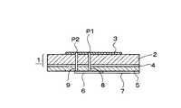
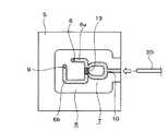
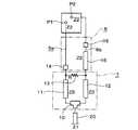
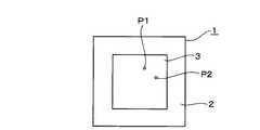
発明の実施の形態について図面を参照して説明すると、図1は本発明の実施形態例に係るパッチアンテナの断面図、図2は該パッチアンテナの底面図、図3は該パッチアンテナの給電回路を示す回路構成図、図4は該パッチアンテナの正面図である。
【0013】
これらの図に示すパッチアンテナは、誘電体基板2の片面にパッチ電極3を設けると共に他面の全面にグラウンド電極4を設けたアンテナ本体1と、このアンテナ本体1のグラウンド電極4側の面に積層状態で固定された回路基板5と、この回路基板5の反アンテナ本体1側の面に配設された90度位相差回路6およびウィルキンソン分配回路7とによって概略構成されている。
【0014】
アンテナ本体1のパッチ電極3には2箇所に給電点P1,P2が設定されている。これらの給電点P1,P2は、2本の給電ピン8,9の各一端部をパッチ電極3の所定位置に半田付けした箇所であり、図1に示すように、各給電ピン8,9は誘電体基板2および回路基板5を貫通している。そして、これら2本の給電ピン8,9の各他端部が90度位相差回路6の相異なる出力端に接続されている。なお、本実施形態例では、誘電体基板2の平面形状を一辺28mmの正方形とし、パッチ電極3の平面形状を一辺16mmの正方形としている。
【0015】
図2,3に示すように、90度位相差回路6の一対の伝送線路6a,6bはウィルキンソン分配回路7の一対の出力端に接続されており、このウィルキンソン分配回路7の入力端は同軸ケーブル20の内導体に接続されている。ここで、ウィルキンソン分配回路7は、入力側が同軸ケーブル20に接続された分岐部10と、この分岐部10の出力側に接続された2本の線路導体11,12と、各線路導体11,12の出力側を連結している抵抗体13とを備えて構成される回路であり、抵抗体13の両端が90度位相差回路6と各線路導体11,12との間に接続されている。2本の線路導体11,12は互いに並列に接続されており、信号波の伝送線路上での波長をλとしたとき、各線路導体11,12の電気長はλ/4に設定されている。また、ウィルキンソン分配回路の入力インピーダンスをZ1、アンテナ本体1の入力インピーダンスをZ2としたとき、各線路導体11,12の特性インピーダンスZ3はZ3=√2×Z1×Z2、抵抗体13の抵抗値RはR=2×Z2に設定されている。具体的には、同軸ケーブル20の特性インピーダンスが50Ωなので、ウィルキンソン分配回路7の入力インピーダンスZ1は50Ωであり、よって各線路導体11,12の特性インピーダンスZ3は約70Ω、抵抗体13の抵抗値Rは100Ωに設定されている。
【0016】
90度位相差回路6は、一方の伝送線路6aに特性インピーダンスが50Ωで電気長が0の線路導体14を備え、かつ他方の伝送線路6bに、特性インピーダンスが50Ωで電気長が0の線路導体15と、特性インピーダンスが50Ωで電気長がλ/4の線路導体16とを備えて構成されている。したがって、伝送線路6aに接続されている給電点P1に供給される信号に比べて、伝送線路6bに接続されている給電点P2に供給される信号は常に位相が90°遅れる。
【0017】
このように構成されたパッチアンテナは、パッチ電極3の二つの直交モードを90°の位相差で励振して円偏波電波を放射させるというものであり、2点給電方式なので広い周波数帯域にわたって軸比特性が良好である。また、このパッチアンテナでは、90度位相差回路6と同軸ケーブル20との間にウィルキンソン分配回路7を介在させているので、パッチ電極3に反射が起きても、この反射が90度位相差回路6を通してウィルキンソン分配回路7の抵抗体13に吸収され、同軸ケーブル20から供給される電力が伝送線路6aと伝送線路6bとに反射なく均等に分配されることになる。そのため、広い周波数帯域にわたって信号波の反射量を大幅に低減することができ、反射特性が広帯域化されている。こうして軸比特性だけでなく反射特性においても帯域幅が広がっているので、本実施形態例に係るパッチアンテナは、広い周波数帯域にわたって電波がカバーできる円偏波アンテナとなっている。
【0018】
また、このパッチアンテナは、アンテナ本体1と回路基板5をコンパクトに一体化しているので、小型で薄型の広帯域なパッチアンテナとして高い実用性が期待できる。なお、本実施形態例では別体のアンテナ本体1と回路基板5とを接合しているが、多層基板の一部を誘電体基板2や回路基板5となす構成にしてもよい。また、2本の給電ピン8,9を用いる代わりに、図示せぬ2本のマイクロストリップラインをパッチ電極3に接続して給電する構成であっても、これらのマイクロストリップラインと同軸ケーブル等の給電線との間に90度位相差回路6およびウィルキンソン分配回路7を介設することにより、パッチアンテナの広帯域化を実現できる。
【0019】
【発明の効果】
本発明は、以上説明したような形態で実施され、以下に記載されるような効果を奏する。
【0020】
パッチ電極の2箇所に設けた給電点に90度位相差回路を接続するという2点給電方式を採用して軸比特性の広帯域化を図りつつ、この90度位相差回路と同軸ケーブル等の給電線との間にウィルキンソン分配回路を介設してアイソレーションを改善し、反射特性の広帯域化も図ったパッチアンテナなので、広い帯域幅の電波がカバーできる小型薄型で実用性の高い円偏波アンテナが得られる。
【図面の簡単な説明】
【図1】本発明の実施形態例に係るパッチアンテナの断面図である。
【図2】該パッチアンテナの底面図である。
【図3】該パッチアンテナの給電回路を示す回路構成図である。
【図4】該パッチアンテナの正面図である。
【符号の説明】
1 アンテナ本体
2 誘電体基板
3 パッチ電極
4 グラウンド電極
5 回路基板
6 90度位相差回路
6a,6b 伝送線路
7 ウィルキンソン分配回路
8,9 給電ピン
10 分岐部
11,12 線路導体
13 抵抗体
20 同軸ケーブル(給電線)
P1,P2 給電点[0001]
TECHNICAL FIELD OF THE INVENTION
The present invention relates to a circularly polarized patch antenna, and more particularly to a feed circuit structure thereof.
[0002]
[Prior art]
In recent years, patch antennas have become widespread as small and thin circularly polarized antennas. This type of patch antenna has a structure in which a patch electrode and a ground electrode are provided on both surfaces of a dielectric substrate to form an antenna body. A predetermined high-frequency signal is fed to a feeding point of the patch electrode, and two orthogonal modes having phases different by 90 ° are provided. Is excited to emit circularly polarized radio waves.
[0003]
There are a single-point feeding method and a two-point feeding method for circularly polarized patch antennas. In general, a single-point feeding method having a simple configuration is adopted. In such a single-point feeding circularly polarized patch antenna, a degenerate separation element (a perturbation element) such as a notch is mounted on a patch electrode, and only one feeding point is set on this patch electrode. For example, one end of a feed pin penetrating the dielectric substrate is connected to the feed point, and the other end of the feed pin is connected to a feed line such as a coaxial cable. The patch antenna of the one-point feeding system configured as described above can adjust 90% to two orthogonal modes having the same amplitude and different resonance lengths by appropriately adjusting the area ratio between the patch electrode and the degenerate separation element and the position of the feeding point. Can be generated, so that the antenna can be operated as a circularly polarized wave antenna.
[0004]
However, a single-point feeding type circularly polarized patch antenna has a narrow resonance frequency band capable of producing a phase difference of 90 ° between the two orthogonal modes, and thus has a low axial ratio characteristic required for a circularly polarized antenna. The bandwidth that can be satisfied, that is, the bandwidth in which the axis ratio of the elliptical polarization is equal to or less than the allowable value is considerably narrow, and there is a problem that it is not possible to widen the band in the axial ratio characteristics.
[0005]
On the other hand, in a two-point feeding type patch antenna, a patch electrode is circular or square and no degenerate separation element is loaded, and signals having phases different from each other by 90 ° are supplied to two feeding points set on the patch electrode. A 90-degree phase difference circuit is provided between the input port of the power supply circuit and the patch antenna. That is, since the phase of the signal going to one feeding point of the patch antenna is always delayed by 90 ° from the phase of the signal going to the other feeding point, the two orthogonal modes of the patch electrode are excited with a phase difference of 90 °. That is, the antenna can be operated as a circularly polarized antenna. In the case of such a two-point feeding type patch antenna, a signal having a phase difference of 90 ° is fed to two feeding points to excite two orthogonal modes, so that the axial ratio characteristics are improved over a wide frequency band.
[0006]
[Problems to be solved by the invention]
As described above, the band ratio in the axial ratio characteristics can be widened by using the two-point feeding system for the circularly polarized patch antenna. However, in the conventional two-point feeding type patch antenna, two points of the patch electrode are provided over a wide frequency band. It is not easy to supply power to the feeding point without reflection, and the amount of reflection of the signal wave tends to increase due to the limitation of the frequency band of the patch antenna itself, so that there is a problem that it is not possible to widen the reflection characteristic. This is considered to be because it is difficult to ensure isolation between the pair of transmission lines of the 90-degree phase difference circuit connected to the patch electrode.
[0007]
The present invention has been made in view of such circumstances of the related art, and an object thereof is to provide a patch antenna for circularly polarized waves that can be used in a wide frequency band by widening an axial ratio characteristic and a reflection characteristic. It is in.
[0008]
[Means for Solving the Problems]
In order to achieve the above-mentioned object, in the patch antenna of the present invention, a patch electrode is provided on one surface of a dielectric substrate and a ground electrode is provided on the other surface, and an antenna body in which a feeding point is set at two places of the patch electrode. A 90-degree phase difference circuit having a pair of output terminals connected to each of the feeding points to generate a 90-degree phase difference between high-frequency signals fed to the two feeding points; The circuit includes a Wilkinson distribution circuit having a pair of output terminals connected thereto, and an input terminal of the Wilkinson distribution circuit is connected to a feeder line so that the antenna body emits circularly polarized radio waves.
[0009]
By connecting a 90-degree phase difference circuit to the feeding points provided at two locations on the patch electrode, a two-point feeding type patch antenna that can achieve a wide band of the axial ratio characteristics can be obtained. If a Wilkinson distribution circuit is interposed between the power supply lines and the like, even if reflection occurs on the patch electrode, this reflection is absorbed by the resistor of the Wilkinson distribution circuit through a 90-degree phase difference circuit, so that a wide frequency The power transmitted from the power supply line can be distributed almost uniformly without reflection over the band and supplied to each power supply point of the patch electrode. As a result, the reflection amount of the signal wave can be greatly reduced, so that the reflection characteristic can be broadened. Therefore, a circularly polarized wave patch antenna having good axial ratio characteristics and good reflection characteristics over a wide frequency band can be obtained.
[0010]
When the input impedance of the Wilkinson distribution circuit is Z1, the input impedance of the antenna main body is Z2, and the wavelength of the high-frequency signal on the transmission line is λ, the Wilkinson distribution circuit is connected to a branch. Both ends of the two line conductors having an electrical length of λ / 4 and a characteristic impedance of √2 × Z1 × Z2, which are parallel to each other, are connected between the 90 ° phase difference circuit and each of the line conductors. This is a circuit including a resistor having a resistance value of 2 × Z2. Generally, since the characteristic impedance of the coaxial cable used for the feeder line is 50Ω, the input impedance of the Wilkinson distribution circuit is 50Ω, the characteristic impedance of each line conductor is about 70Ω, and the resistance value of the resistor is 100Ω.
[0011]
Further, in the patch antenna provided with such a feeder circuit, the 90-degree phase difference circuit and the Wilkinson distribution circuit are fixed to the ground electrode side surface of the antenna main body in a stacked state, and the anti-antenna main body of the circuit board is fixed. And one end of each of two power supply pins penetrating the dielectric substrate and the circuit board is connected to a different one of the power supply points, and the other end of each of the two power supply pins is It is preferable that the side of the antenna is connected to different output terminals of the 90-degree phase difference circuit because a compact and wide band patch antenna in which the antenna body and the circuit board are compactly integrated can be obtained. In this case, the dielectric substrate of the antenna body and the circuit board for the power supply circuit may be a part of the multilayer board. However, even if two microstrip lines are connected to the patch electrodes and power is supplied instead of using two power supply pins, a phase difference of 90 degrees between these microstrip lines and the power supply line is provided. By providing the circuit and the Wilkinson distribution circuit, the band of the patch antenna can be widened.
[0012]
BEST MODE FOR CARRYING OUT THE INVENTION
FIG. 1 is a cross-sectional view of a patch antenna according to an embodiment of the present invention, FIG. 2 is a bottom view of the patch antenna, and FIG. 3 is a feeder circuit of the patch antenna. FIG. 4 is a front view of the patch antenna.
[0013]
The patch antenna shown in these figures has an
[0014]
Feed points P1 and P2 are set at two places on the
[0015]
As shown in FIGS. 2 and 3, a pair of
[0016]
The 90-degree
[0017]
The patch antenna thus configured excites two orthogonal modes of the
[0018]
In addition, since this patch antenna integrates the
[0019]
【The invention's effect】
The present invention is implemented in the form described above, and has the following effects.
[0020]
A 90-degree phase difference circuit, in which a 90-degree phase difference circuit is connected to feed points provided at two locations on the patch electrode, is used to widen the axial ratio characteristics. A small, thin, highly practical circularly polarized antenna that can cover radio waves of a wide bandwidth because it is a patch antenna that improves isolation by providing a Wilkinson distribution circuit between the wires and improves isolation and broadens the reflection characteristics. Is obtained.
[Brief description of the drawings]
FIG. 1 is a sectional view of a patch antenna according to an embodiment of the present invention.
FIG. 2 is a bottom view of the patch antenna.
FIG. 3 is a circuit diagram showing a feed circuit of the patch antenna.
FIG. 4 is a front view of the patch antenna.
[Explanation of symbols]
DESCRIPTION OF
P1, P2 feeding point
Claims (4)
Translated fromJapanesePriority Applications (3)
| Application Number | Priority Date | Filing Date | Title |
|---|---|---|---|
| JP2002207079AJP2004056204A (en) | 2002-07-16 | 2002-07-16 | Patch antenna |
| EP03253862AEP1383200A1 (en) | 2002-07-16 | 2003-06-27 | Circularly polarized wave patch antenna |
| US10/615,113US6952183B2 (en) | 2002-07-16 | 2003-07-08 | Circularly-polarized-wave patch antenna which can be used in a wide frequency band |
Applications Claiming Priority (1)
| Application Number | Priority Date | Filing Date | Title |
|---|---|---|---|
| JP2002207079AJP2004056204A (en) | 2002-07-16 | 2002-07-16 | Patch antenna |
Publications (1)
| Publication Number | Publication Date |
|---|---|
| JP2004056204Atrue JP2004056204A (en) | 2004-02-19 |
Family
ID=29774613
Family Applications (1)
| Application Number | Title | Priority Date | Filing Date |
|---|---|---|---|
| JP2002207079AWithdrawnJP2004056204A (en) | 2002-07-16 | 2002-07-16 | Patch antenna |
Country Status (3)
| Country | Link |
|---|---|
| US (1) | US6952183B2 (en) |
| EP (1) | EP1383200A1 (en) |
| JP (1) | JP2004056204A (en) |
Cited By (9)
| Publication number | Priority date | Publication date | Assignee | Title |
|---|---|---|---|---|
| KR100685512B1 (en)* | 2004-11-29 | 2007-02-27 | 주식회사 케이티프리텔 | Microstrip antenna for receiving broadcast signal |
| KR100933746B1 (en)* | 2007-05-30 | 2009-12-24 | 주식회사 이엠따블유안테나 | Dual Band Circular Polarization Antenna |
| WO2012039465A1 (en)* | 2010-09-24 | 2012-03-29 | 古河電気工業株式会社 | Antenna system |
| JP2013016947A (en)* | 2011-07-01 | 2013-01-24 | Mitsumi Electric Co Ltd | Antenna device |
| WO2015004992A1 (en)* | 2013-07-09 | 2015-01-15 | 株式会社ヨコオ | Micro-strip antenna |
| JP2015530055A (en)* | 2012-09-11 | 2015-10-08 | アルカテル−ルーセント | Integrated antenna with high radiation efficiency |
| JP2016149687A (en)* | 2015-02-13 | 2016-08-18 | 富士通株式会社 | Antenna device |
| WO2020050341A1 (en)* | 2018-09-07 | 2020-03-12 | 株式会社村田製作所 | Antenna element, antenna module, and communication device |
| WO2021140738A1 (en)* | 2020-01-06 | 2021-07-15 | 原田工業株式会社 | Power feeder circuit for circularly polarized antenna |
Families Citing this family (164)
| Publication number | Priority date | Publication date | Assignee | Title |
|---|---|---|---|---|
| JP3854976B2 (en)* | 2004-04-26 | 2006-12-06 | 松下電器産業株式会社 | Foldable portable radio |
| US7546137B2 (en) | 2005-02-28 | 2009-06-09 | Sirit Technologies Inc. | Power control loop and LO generation method |
| US20060220962A1 (en)* | 2005-02-28 | 2006-10-05 | D Hont Loek J | Circularly polorized square patch antenna |
| US20070066224A1 (en)* | 2005-02-28 | 2007-03-22 | Sirit, Inc. | High efficiency RF amplifier and envelope modulator |
| US20090028074A1 (en)* | 2005-06-22 | 2009-01-29 | Knox Michael E | Antenna feed network for full duplex communication |
| US8111640B2 (en) | 2005-06-22 | 2012-02-07 | Knox Michael E | Antenna feed network for full duplex communication |
| US9780437B2 (en) | 2005-06-22 | 2017-10-03 | Michael E. Knox | Antenna feed network for full duplex communication |
| TWI269487B (en)* | 2005-11-01 | 2006-12-21 | Tatung Co | A circular polarized antenna |
| US8750173B2 (en) | 2006-12-29 | 2014-06-10 | Mode-1 Corporation | High isolation signal routing assembly for full duplex communication |
| WO2008082638A1 (en)* | 2006-12-29 | 2008-07-10 | Knox Michael E | High isolation signal routing assembly for full duplex communication |
| US20100156607A1 (en)* | 2008-12-19 | 2010-06-24 | Thomas Lankes | Method for activating an RFID antenna and an associated RFID antenna system |
| IT1395411B1 (en)* | 2009-07-24 | 2012-09-14 | Com Tech Srl | HYBRID DIVIDER FOR UHF |
| DE102010028265A1 (en)* | 2010-04-27 | 2011-10-27 | Robert Bosch Gmbh | Antenna device for transmitting and receiving electromagnetic waves |
| US9113347B2 (en) | 2012-12-05 | 2015-08-18 | At&T Intellectual Property I, Lp | Backhaul link for distributed antenna system |
| US10009065B2 (en) | 2012-12-05 | 2018-06-26 | At&T Intellectual Property I, L.P. | Backhaul link for distributed antenna system |
| US9999038B2 (en) | 2013-05-31 | 2018-06-12 | At&T Intellectual Property I, L.P. | Remote distributed antenna system |
| US9525524B2 (en) | 2013-05-31 | 2016-12-20 | At&T Intellectual Property I, L.P. | Remote distributed antenna system |
| US8897697B1 (en) | 2013-11-06 | 2014-11-25 | At&T Intellectual Property I, Lp | Millimeter-wave surface-wave communications |
| US9692101B2 (en) | 2014-08-26 | 2017-06-27 | At&T Intellectual Property I, L.P. | Guided wave couplers for coupling electromagnetic waves between a waveguide surface and a surface of a wire |
| US9768833B2 (en) | 2014-09-15 | 2017-09-19 | At&T Intellectual Property I, L.P. | Method and apparatus for sensing a condition in a transmission medium of electromagnetic waves |
| US10063280B2 (en) | 2014-09-17 | 2018-08-28 | At&T Intellectual Property I, L.P. | Monitoring and mitigating conditions in a communication network |
| US9615269B2 (en) | 2014-10-02 | 2017-04-04 | At&T Intellectual Property I, L.P. | Method and apparatus that provides fault tolerance in a communication network |
| US9685992B2 (en) | 2014-10-03 | 2017-06-20 | At&T Intellectual Property I, L.P. | Circuit panel network and methods thereof |
| US9503189B2 (en) | 2014-10-10 | 2016-11-22 | At&T Intellectual Property I, L.P. | Method and apparatus for arranging communication sessions in a communication system |
| US9762289B2 (en) | 2014-10-14 | 2017-09-12 | At&T Intellectual Property I, L.P. | Method and apparatus for transmitting or receiving signals in a transportation system |
| US9973299B2 (en) | 2014-10-14 | 2018-05-15 | At&T Intellectual Property I, L.P. | Method and apparatus for adjusting a mode of communication in a communication network |
| US9520945B2 (en) | 2014-10-21 | 2016-12-13 | At&T Intellectual Property I, L.P. | Apparatus for providing communication services and methods thereof |
| US9312919B1 (en) | 2014-10-21 | 2016-04-12 | At&T Intellectual Property I, Lp | Transmission device with impairment compensation and methods for use therewith |
| US9780834B2 (en) | 2014-10-21 | 2017-10-03 | At&T Intellectual Property I, L.P. | Method and apparatus for transmitting electromagnetic waves |
| US9627768B2 (en) | 2014-10-21 | 2017-04-18 | At&T Intellectual Property I, L.P. | Guided-wave transmission device with non-fundamental mode propagation and methods for use therewith |
| US9653770B2 (en) | 2014-10-21 | 2017-05-16 | At&T Intellectual Property I, L.P. | Guided wave coupler, coupling module and methods for use therewith |
| US9769020B2 (en) | 2014-10-21 | 2017-09-19 | At&T Intellectual Property I, L.P. | Method and apparatus for responding to events affecting communications in a communication network |
| US9577306B2 (en) | 2014-10-21 | 2017-02-21 | At&T Intellectual Property I, L.P. | Guided-wave transmission device and methods for use therewith |
| US9742462B2 (en) | 2014-12-04 | 2017-08-22 | At&T Intellectual Property I, L.P. | Transmission medium and communication interfaces and methods for use therewith |
| US10340573B2 (en) | 2016-10-26 | 2019-07-02 | At&T Intellectual Property I, L.P. | Launcher with cylindrical coupling device and methods for use therewith |
| US9997819B2 (en) | 2015-06-09 | 2018-06-12 | At&T Intellectual Property I, L.P. | Transmission medium and method for facilitating propagation of electromagnetic waves via a core |
| US9461706B1 (en) | 2015-07-31 | 2016-10-04 | At&T Intellectual Property I, Lp | Method and apparatus for exchanging communication signals |
| US9954287B2 (en) | 2014-11-20 | 2018-04-24 | At&T Intellectual Property I, L.P. | Apparatus for converting wireless signals and electromagnetic waves and methods thereof |
| US10243784B2 (en) | 2014-11-20 | 2019-03-26 | At&T Intellectual Property I, L.P. | System for generating topology information and methods thereof |
| US9800327B2 (en) | 2014-11-20 | 2017-10-24 | At&T Intellectual Property I, L.P. | Apparatus for controlling operations of a communication device and methods thereof |
| US10009067B2 (en) | 2014-12-04 | 2018-06-26 | At&T Intellectual Property I, L.P. | Method and apparatus for configuring a communication interface |
| US9544006B2 (en) | 2014-11-20 | 2017-01-10 | At&T Intellectual Property I, L.P. | Transmission device with mode division multiplexing and methods for use therewith |
| US10144036B2 (en) | 2015-01-30 | 2018-12-04 | At&T Intellectual Property I, L.P. | Method and apparatus for mitigating interference affecting a propagation of electromagnetic waves guided by a transmission medium |
| US9876570B2 (en) | 2015-02-20 | 2018-01-23 | At&T Intellectual Property I, Lp | Guided-wave transmission device with non-fundamental mode propagation and methods for use therewith |
| US9749013B2 (en) | 2015-03-17 | 2017-08-29 | At&T Intellectual Property I, L.P. | Method and apparatus for reducing attenuation of electromagnetic waves guided by a transmission medium |
| CN104767019B (en)* | 2015-04-21 | 2017-07-04 | 中国电子科技集团公司第四十一研究所 | A kind of power distribution and synthesizer based on ultra wide band coaxial impedance converter |
| US9705561B2 (en) | 2015-04-24 | 2017-07-11 | At&T Intellectual Property I, L.P. | Directional coupling device and methods for use therewith |
| US10224981B2 (en) | 2015-04-24 | 2019-03-05 | At&T Intellectual Property I, Lp | Passive electrical coupling device and methods for use therewith |
| US9948354B2 (en) | 2015-04-28 | 2018-04-17 | At&T Intellectual Property I, L.P. | Magnetic coupling device with reflective plate and methods for use therewith |
| US9793954B2 (en) | 2015-04-28 | 2017-10-17 | At&T Intellectual Property I, L.P. | Magnetic coupling device and methods for use therewith |
| US9748626B2 (en) | 2015-05-14 | 2017-08-29 | At&T Intellectual Property I, L.P. | Plurality of cables having different cross-sectional shapes which are bundled together to form a transmission medium |
| US9871282B2 (en) | 2015-05-14 | 2018-01-16 | At&T Intellectual Property I, L.P. | At least one transmission medium having a dielectric surface that is covered at least in part by a second dielectric |
| US9490869B1 (en) | 2015-05-14 | 2016-11-08 | At&T Intellectual Property I, L.P. | Transmission medium having multiple cores and methods for use therewith |
| US10650940B2 (en) | 2015-05-15 | 2020-05-12 | At&T Intellectual Property I, L.P. | Transmission medium having a conductive material and methods for use therewith |
| US9917341B2 (en) | 2015-05-27 | 2018-03-13 | At&T Intellectual Property I, L.P. | Apparatus and method for launching electromagnetic waves and for modifying radial dimensions of the propagating electromagnetic waves |
| US10812174B2 (en) | 2015-06-03 | 2020-10-20 | At&T Intellectual Property I, L.P. | Client node device and methods for use therewith |
| US10103801B2 (en) | 2015-06-03 | 2018-10-16 | At&T Intellectual Property I, L.P. | Host node device and methods for use therewith |
| US9866309B2 (en) | 2015-06-03 | 2018-01-09 | At&T Intellectual Property I, Lp | Host node device and methods for use therewith |
| US9912381B2 (en) | 2015-06-03 | 2018-03-06 | At&T Intellectual Property I, Lp | Network termination and methods for use therewith |
| US9913139B2 (en) | 2015-06-09 | 2018-03-06 | At&T Intellectual Property I, L.P. | Signal fingerprinting for authentication of communicating devices |
| US10142086B2 (en) | 2015-06-11 | 2018-11-27 | At&T Intellectual Property I, L.P. | Repeater and methods for use therewith |
| US9608692B2 (en) | 2015-06-11 | 2017-03-28 | At&T Intellectual Property I, L.P. | Repeater and methods for use therewith |
| US9820146B2 (en) | 2015-06-12 | 2017-11-14 | At&T Intellectual Property I, L.P. | Method and apparatus for authentication and identity management of communicating devices |
| US9667317B2 (en) | 2015-06-15 | 2017-05-30 | At&T Intellectual Property I, L.P. | Method and apparatus for providing security using network traffic adjustments |
| US9640850B2 (en) | 2015-06-25 | 2017-05-02 | At&T Intellectual Property I, L.P. | Methods and apparatus for inducing a non-fundamental wave mode on a transmission medium |
| US9509415B1 (en) | 2015-06-25 | 2016-11-29 | At&T Intellectual Property I, L.P. | Methods and apparatus for inducing a fundamental wave mode on a transmission medium |
| US9865911B2 (en) | 2015-06-25 | 2018-01-09 | At&T Intellectual Property I, L.P. | Waveguide system for slot radiating first electromagnetic waves that are combined into a non-fundamental wave mode second electromagnetic wave on a transmission medium |
| US10148016B2 (en) | 2015-07-14 | 2018-12-04 | At&T Intellectual Property I, L.P. | Apparatus and methods for communicating utilizing an antenna array |
| US10170840B2 (en) | 2015-07-14 | 2019-01-01 | At&T Intellectual Property I, L.P. | Apparatus and methods for sending or receiving electromagnetic signals |
| US9722318B2 (en) | 2015-07-14 | 2017-08-01 | At&T Intellectual Property I, L.P. | Method and apparatus for coupling an antenna to a device |
| US10320586B2 (en) | 2015-07-14 | 2019-06-11 | At&T Intellectual Property I, L.P. | Apparatus and methods for generating non-interfering electromagnetic waves on an insulated transmission medium |
| US9882257B2 (en) | 2015-07-14 | 2018-01-30 | At&T Intellectual Property I, L.P. | Method and apparatus for launching a wave mode that mitigates interference |
| US9628116B2 (en) | 2015-07-14 | 2017-04-18 | At&T Intellectual Property I, L.P. | Apparatus and methods for transmitting wireless signals |
| US9847566B2 (en) | 2015-07-14 | 2017-12-19 | At&T Intellectual Property I, L.P. | Method and apparatus for adjusting a field of a signal to mitigate interference |
| US10205655B2 (en) | 2015-07-14 | 2019-02-12 | At&T Intellectual Property I, L.P. | Apparatus and methods for communicating utilizing an antenna array and multiple communication paths |
| US10033107B2 (en) | 2015-07-14 | 2018-07-24 | At&T Intellectual Property I, L.P. | Method and apparatus for coupling an antenna to a device |
| US9853342B2 (en) | 2015-07-14 | 2017-12-26 | At&T Intellectual Property I, L.P. | Dielectric transmission medium connector and methods for use therewith |
| US10341142B2 (en) | 2015-07-14 | 2019-07-02 | At&T Intellectual Property I, L.P. | Apparatus and methods for generating non-interfering electromagnetic waves on an uninsulated conductor |
| US10033108B2 (en) | 2015-07-14 | 2018-07-24 | At&T Intellectual Property I, L.P. | Apparatus and methods for generating an electromagnetic wave having a wave mode that mitigates interference |
| US10044409B2 (en) | 2015-07-14 | 2018-08-07 | At&T Intellectual Property I, L.P. | Transmission medium and methods for use therewith |
| US9608740B2 (en) | 2015-07-15 | 2017-03-28 | At&T Intellectual Property I, L.P. | Method and apparatus for launching a wave mode that mitigates interference |
| US9793951B2 (en) | 2015-07-15 | 2017-10-17 | At&T Intellectual Property I, L.P. | Method and apparatus for launching a wave mode that mitigates interference |
| US10090606B2 (en) | 2015-07-15 | 2018-10-02 | At&T Intellectual Property I, L.P. | Antenna system with dielectric array and methods for use therewith |
| US9749053B2 (en) | 2015-07-23 | 2017-08-29 | At&T Intellectual Property I, L.P. | Node device, repeater and methods for use therewith |
| US9871283B2 (en) | 2015-07-23 | 2018-01-16 | At&T Intellectual Property I, Lp | Transmission medium having a dielectric core comprised of plural members connected by a ball and socket configuration |
| US9948333B2 (en) | 2015-07-23 | 2018-04-17 | At&T Intellectual Property I, L.P. | Method and apparatus for wireless communications to mitigate interference |
| US9912027B2 (en) | 2015-07-23 | 2018-03-06 | At&T Intellectual Property I, L.P. | Method and apparatus for exchanging communication signals |
| US9735833B2 (en) | 2015-07-31 | 2017-08-15 | At&T Intellectual Property I, L.P. | Method and apparatus for communications management in a neighborhood network |
| US9967173B2 (en) | 2015-07-31 | 2018-05-08 | At&T Intellectual Property I, L.P. | Method and apparatus for authentication and identity management of communicating devices |
| CN205029009U (en)* | 2015-08-24 | 2016-02-10 | 中兴通讯股份有限公司 | Two wireless radio frequency identification antennas of circular polarization in broadband |
| US9904535B2 (en) | 2015-09-14 | 2018-02-27 | At&T Intellectual Property I, L.P. | Method and apparatus for distributing software |
| US10136434B2 (en) | 2015-09-16 | 2018-11-20 | At&T Intellectual Property I, L.P. | Method and apparatus for use with a radio distributed antenna system having an ultra-wideband control channel |
| US10079661B2 (en) | 2015-09-16 | 2018-09-18 | At&T Intellectual Property I, L.P. | Method and apparatus for use with a radio distributed antenna system having a clock reference |
| US10009063B2 (en) | 2015-09-16 | 2018-06-26 | At&T Intellectual Property I, L.P. | Method and apparatus for use with a radio distributed antenna system having an out-of-band reference signal |
| US9769128B2 (en) | 2015-09-28 | 2017-09-19 | At&T Intellectual Property I, L.P. | Method and apparatus for encryption of communications over a network |
| US9729197B2 (en) | 2015-10-01 | 2017-08-08 | At&T Intellectual Property I, L.P. | Method and apparatus for communicating network management traffic over a network |
| US9876264B2 (en) | 2015-10-02 | 2018-01-23 | At&T Intellectual Property I, Lp | Communication system, guided wave switch and methods for use therewith |
| US10355367B2 (en) | 2015-10-16 | 2019-07-16 | At&T Intellectual Property I, L.P. | Antenna structure for exchanging wireless signals |
| US10665942B2 (en) | 2015-10-16 | 2020-05-26 | At&T Intellectual Property I, L.P. | Method and apparatus for adjusting wireless communications |
| US9912419B1 (en) | 2016-08-24 | 2018-03-06 | At&T Intellectual Property I, L.P. | Method and apparatus for managing a fault in a distributed antenna system |
| US9860075B1 (en) | 2016-08-26 | 2018-01-02 | At&T Intellectual Property I, L.P. | Method and communication node for broadband distribution |
| US10291311B2 (en) | 2016-09-09 | 2019-05-14 | At&T Intellectual Property I, L.P. | Method and apparatus for mitigating a fault in a distributed antenna system |
| US11032819B2 (en) | 2016-09-15 | 2021-06-08 | At&T Intellectual Property I, L.P. | Method and apparatus for use with a radio distributed antenna system having a control channel reference signal |
| US10135147B2 (en) | 2016-10-18 | 2018-11-20 | At&T Intellectual Property I, L.P. | Apparatus and methods for launching guided waves via an antenna |
| US10135146B2 (en) | 2016-10-18 | 2018-11-20 | At&T Intellectual Property I, L.P. | Apparatus and methods for launching guided waves via circuits |
| US10340600B2 (en) | 2016-10-18 | 2019-07-02 | At&T Intellectual Property I, L.P. | Apparatus and methods for launching guided waves via plural waveguide systems |
| US10374316B2 (en) | 2016-10-21 | 2019-08-06 | At&T Intellectual Property I, L.P. | System and dielectric antenna with non-uniform dielectric |
| US9991580B2 (en) | 2016-10-21 | 2018-06-05 | At&T Intellectual Property I, L.P. | Launcher and coupling system for guided wave mode cancellation |
| US10811767B2 (en) | 2016-10-21 | 2020-10-20 | At&T Intellectual Property I, L.P. | System and dielectric antenna with convex dielectric radome |
| US9876605B1 (en) | 2016-10-21 | 2018-01-23 | At&T Intellectual Property I, L.P. | Launcher and coupling system to support desired guided wave mode |
| US10312567B2 (en) | 2016-10-26 | 2019-06-04 | At&T Intellectual Property I, L.P. | Launcher with planar strip antenna and methods for use therewith |
| US10224634B2 (en) | 2016-11-03 | 2019-03-05 | At&T Intellectual Property I, L.P. | Methods and apparatus for adjusting an operational characteristic of an antenna |
| US10498044B2 (en) | 2016-11-03 | 2019-12-03 | At&T Intellectual Property I, L.P. | Apparatus for configuring a surface of an antenna |
| US10225025B2 (en) | 2016-11-03 | 2019-03-05 | At&T Intellectual Property I, L.P. | Method and apparatus for detecting a fault in a communication system |
| US10291334B2 (en) | 2016-11-03 | 2019-05-14 | At&T Intellectual Property I, L.P. | System for detecting a fault in a communication system |
| US10090594B2 (en) | 2016-11-23 | 2018-10-02 | At&T Intellectual Property I, L.P. | Antenna system having structural configurations for assembly |
| US10178445B2 (en) | 2016-11-23 | 2019-01-08 | At&T Intellectual Property I, L.P. | Methods, devices, and systems for load balancing between a plurality of waveguides |
| US10340601B2 (en) | 2016-11-23 | 2019-07-02 | At&T Intellectual Property I, L.P. | Multi-antenna system and methods for use therewith |
| US10340603B2 (en) | 2016-11-23 | 2019-07-02 | At&T Intellectual Property I, L.P. | Antenna system having shielded structural configurations for assembly |
| US10535928B2 (en) | 2016-11-23 | 2020-01-14 | At&T Intellectual Property I, L.P. | Antenna system and methods for use therewith |
| US10305190B2 (en) | 2016-12-01 | 2019-05-28 | At&T Intellectual Property I, L.P. | Reflecting dielectric antenna system and methods for use therewith |
| US10361489B2 (en) | 2016-12-01 | 2019-07-23 | At&T Intellectual Property I, L.P. | Dielectric dish antenna system and methods for use therewith |
| US10135145B2 (en) | 2016-12-06 | 2018-11-20 | At&T Intellectual Property I, L.P. | Apparatus and methods for generating an electromagnetic wave along a transmission medium |
| US10727599B2 (en) | 2016-12-06 | 2020-07-28 | At&T Intellectual Property I, L.P. | Launcher with slot antenna and methods for use therewith |
| US10755542B2 (en) | 2016-12-06 | 2020-08-25 | At&T Intellectual Property I, L.P. | Method and apparatus for surveillance via guided wave communication |
| US10637149B2 (en) | 2016-12-06 | 2020-04-28 | At&T Intellectual Property I, L.P. | Injection molded dielectric antenna and methods for use therewith |
| US10439675B2 (en) | 2016-12-06 | 2019-10-08 | At&T Intellectual Property I, L.P. | Method and apparatus for repeating guided wave communication signals |
| US10819035B2 (en) | 2016-12-06 | 2020-10-27 | At&T Intellectual Property I, L.P. | Launcher with helical antenna and methods for use therewith |
| US9927517B1 (en) | 2016-12-06 | 2018-03-27 | At&T Intellectual Property I, L.P. | Apparatus and methods for sensing rainfall |
| US10020844B2 (en) | 2016-12-06 | 2018-07-10 | T&T Intellectual Property I, L.P. | Method and apparatus for broadcast communication via guided waves |
| US10326494B2 (en) | 2016-12-06 | 2019-06-18 | At&T Intellectual Property I, L.P. | Apparatus for measurement de-embedding and methods for use therewith |
| US10382976B2 (en) | 2016-12-06 | 2019-08-13 | At&T Intellectual Property I, L.P. | Method and apparatus for managing wireless communications based on communication paths and network device positions |
| US10694379B2 (en) | 2016-12-06 | 2020-06-23 | At&T Intellectual Property I, L.P. | Waveguide system with device-based authentication and methods for use therewith |
| US10359749B2 (en) | 2016-12-07 | 2019-07-23 | At&T Intellectual Property I, L.P. | Method and apparatus for utilities management via guided wave communication |
| US10139820B2 (en) | 2016-12-07 | 2018-11-27 | At&T Intellectual Property I, L.P. | Method and apparatus for deploying equipment of a communication system |
| US10168695B2 (en) | 2016-12-07 | 2019-01-01 | At&T Intellectual Property I, L.P. | Method and apparatus for controlling an unmanned aircraft |
| US10243270B2 (en) | 2016-12-07 | 2019-03-26 | At&T Intellectual Property I, L.P. | Beam adaptive multi-feed dielectric antenna system and methods for use therewith |
| US10389029B2 (en) | 2016-12-07 | 2019-08-20 | At&T Intellectual Property I, L.P. | Multi-feed dielectric antenna system with core selection and methods for use therewith |
| US10547348B2 (en) | 2016-12-07 | 2020-01-28 | At&T Intellectual Property I, L.P. | Method and apparatus for switching transmission mediums in a communication system |
| US10027397B2 (en) | 2016-12-07 | 2018-07-17 | At&T Intellectual Property I, L.P. | Distributed antenna system and methods for use therewith |
| US9893795B1 (en) | 2016-12-07 | 2018-02-13 | At&T Intellectual Property I, Lp | Method and repeater for broadband distribution |
| US10446936B2 (en) | 2016-12-07 | 2019-10-15 | At&T Intellectual Property I, L.P. | Multi-feed dielectric antenna system and methods for use therewith |
| US10777873B2 (en) | 2016-12-08 | 2020-09-15 | At&T Intellectual Property I, L.P. | Method and apparatus for mounting network devices |
| US10938108B2 (en) | 2016-12-08 | 2021-03-02 | At&T Intellectual Property I, L.P. | Frequency selective multi-feed dielectric antenna system and methods for use therewith |
| US10103422B2 (en) | 2016-12-08 | 2018-10-16 | At&T Intellectual Property I, L.P. | Method and apparatus for mounting network devices |
| US10601494B2 (en) | 2016-12-08 | 2020-03-24 | At&T Intellectual Property I, L.P. | Dual-band communication device and method for use therewith |
| US10411356B2 (en) | 2016-12-08 | 2019-09-10 | At&T Intellectual Property I, L.P. | Apparatus and methods for selectively targeting communication devices with an antenna array |
| US10326689B2 (en) | 2016-12-08 | 2019-06-18 | At&T Intellectual Property I, L.P. | Method and system for providing alternative communication paths |
| US10069535B2 (en) | 2016-12-08 | 2018-09-04 | At&T Intellectual Property I, L.P. | Apparatus and methods for launching electromagnetic waves having a certain electric field structure |
| US10389037B2 (en) | 2016-12-08 | 2019-08-20 | At&T Intellectual Property I, L.P. | Apparatus and methods for selecting sections of an antenna array and use therewith |
| US9998870B1 (en) | 2016-12-08 | 2018-06-12 | At&T Intellectual Property I, L.P. | Method and apparatus for proximity sensing |
| US9911020B1 (en) | 2016-12-08 | 2018-03-06 | At&T Intellectual Property I, L.P. | Method and apparatus for tracking via a radio frequency identification device |
| US10916969B2 (en) | 2016-12-08 | 2021-02-09 | At&T Intellectual Property I, L.P. | Method and apparatus for providing power using an inductive coupling |
| US10530505B2 (en) | 2016-12-08 | 2020-01-07 | At&T Intellectual Property I, L.P. | Apparatus and methods for launching electromagnetic waves along a transmission medium |
| US10264586B2 (en) | 2016-12-09 | 2019-04-16 | At&T Mobility Ii Llc | Cloud-based packet controller and methods for use therewith |
| US10340983B2 (en) | 2016-12-09 | 2019-07-02 | At&T Intellectual Property I, L.P. | Method and apparatus for surveying remote sites via guided wave communications |
| US9838896B1 (en) | 2016-12-09 | 2017-12-05 | At&T Intellectual Property I, L.P. | Method and apparatus for assessing network coverage |
| US9973940B1 (en) | 2017-02-27 | 2018-05-15 | At&T Intellectual Property I, L.P. | Apparatus and methods for dynamic impedance matching of a guided wave launcher |
| US10298293B2 (en) | 2017-03-13 | 2019-05-21 | At&T Intellectual Property I, L.P. | Apparatus of communication utilizing wireless network devices |
| CN108054501B (en)* | 2017-10-31 | 2020-08-07 | 南京邮电大学 | A Broadband Circularly Polarized Antenna with Equal Ripple Axial Ratio Response |
| KR102482071B1 (en)* | 2018-02-14 | 2022-12-28 | 삼성전자주식회사 | Antenna using multi-feeding and electronic device including the same |
| CN109638422B (en)* | 2018-11-15 | 2021-02-05 | 中国电子科技集团公司第三十八研究所 | Broadband circularly polarized common-caliber communication navigation array antenna |
| CN110534891B (en)* | 2019-09-10 | 2024-07-23 | 桂林电子科技大学 | Broadband polarization adjustable antenna based on composite left-right hand transmission line |
| CN117650366B (en)* | 2024-01-30 | 2024-04-05 | 北京宏动科技股份有限公司 | Ultra-wideband circularly polarized antenna assembly and related electronic equipment |
Citations (10)
| Publication number | Priority date | Publication date | Assignee | Title |
|---|---|---|---|---|
| JPS63125008A (en)* | 1986-11-15 | 1988-05-28 | Matsushita Electric Works Ltd | Plane antenna for circularly polarized wave |
| JPH01293704A (en)* | 1988-05-23 | 1989-11-27 | A T R Koudenpa Tsushin Kenkyusho:Kk | Circularly polarized wave microstrip antenna |
| JPH0590826A (en)* | 1991-09-26 | 1993-04-09 | Toshiba Corp | Micro strip antenna |
| JPH06326510A (en)* | 1992-11-18 | 1994-11-25 | Toshiba Corp | Beam scanning antenna and array antenna |
| JP2868197B2 (en)* | 1991-11-14 | 1999-03-10 | ダソー エレクトロニック ソシエテ アノニム | An improved microstrip antenna device especially for satellite telephony. |
| JP2000101341A (en)* | 1998-09-24 | 2000-04-07 | Mitsubishi Electric Corp | Microstrip array antenna |
| JP2000138525A (en)* | 1998-10-30 | 2000-05-16 | Mitsubishi Electric Corp | Microstrip antenna and microstrip antenna substrate |
| JP2000261235A (en)* | 1999-03-05 | 2000-09-22 | Mitsubishi Electric Corp | Triplate line feed type microstrip antenna |
| JP3167342B2 (en)* | 1991-03-14 | 2001-05-21 | 株式会社東芝 | Transmitting and receiving circularly polarized antenna |
| JP3288174B2 (en)* | 1994-05-16 | 2002-06-04 | 株式会社日立製作所 | Array antenna capable of controlling linear polarization plane and satellite communication earth station having the same |
Family Cites Families (8)
| Publication number | Priority date | Publication date | Assignee | Title |
|---|---|---|---|---|
| US4749996A (en)* | 1983-08-29 | 1988-06-07 | Allied-Signal Inc. | Double tuned, coupled microstrip antenna |
| US4973972A (en)* | 1989-09-07 | 1990-11-27 | The United States Of America As Represented By The Administrator Of The National Aeronautics And Space Adminstration | Stripline feed for a microstrip array of patch elements with teardrop shaped probes |
| EP0432647B1 (en)* | 1989-12-11 | 1995-06-21 | Kabushiki Kaisha Toyota Chuo Kenkyusho | Mobile antenna system |
| JP2551919B2 (en) | 1994-03-23 | 1996-11-06 | 森田産業株式会社 | Far-infrared heating device and tufted original heat treatment method |
| KR100233084B1 (en)* | 1997-04-26 | 1999-12-01 | 윤종용 | High frequency power divider |
| US5940030A (en)* | 1998-03-18 | 1999-08-17 | Lucent Technologies, Inc. | Steerable phased-array antenna having series feed network |
| DE10008602C2 (en) | 2000-02-24 | 2003-07-10 | Siemens Ag | Data processing device with power supply and power supply for data processing devices |
| DE60136820D1 (en) | 2000-07-11 | 2009-01-15 | Thomson Licensing | POWER ADAPTER FOR A MODULAR POWER SUPPLY NETWORK |
- 2002
- 2002-07-16JPJP2002207079Apatent/JP2004056204A/ennot_activeWithdrawn
- 2003
- 2003-06-27EPEP03253862Apatent/EP1383200A1/ennot_activeWithdrawn
- 2003-07-08USUS10/615,113patent/US6952183B2/ennot_activeExpired - Fee Related
Patent Citations (10)
| Publication number | Priority date | Publication date | Assignee | Title |
|---|---|---|---|---|
| JPS63125008A (en)* | 1986-11-15 | 1988-05-28 | Matsushita Electric Works Ltd | Plane antenna for circularly polarized wave |
| JPH01293704A (en)* | 1988-05-23 | 1989-11-27 | A T R Koudenpa Tsushin Kenkyusho:Kk | Circularly polarized wave microstrip antenna |
| JP3167342B2 (en)* | 1991-03-14 | 2001-05-21 | 株式会社東芝 | Transmitting and receiving circularly polarized antenna |
| JPH0590826A (en)* | 1991-09-26 | 1993-04-09 | Toshiba Corp | Micro strip antenna |
| JP2868197B2 (en)* | 1991-11-14 | 1999-03-10 | ダソー エレクトロニック ソシエテ アノニム | An improved microstrip antenna device especially for satellite telephony. |
| JPH06326510A (en)* | 1992-11-18 | 1994-11-25 | Toshiba Corp | Beam scanning antenna and array antenna |
| JP3288174B2 (en)* | 1994-05-16 | 2002-06-04 | 株式会社日立製作所 | Array antenna capable of controlling linear polarization plane and satellite communication earth station having the same |
| JP2000101341A (en)* | 1998-09-24 | 2000-04-07 | Mitsubishi Electric Corp | Microstrip array antenna |
| JP2000138525A (en)* | 1998-10-30 | 2000-05-16 | Mitsubishi Electric Corp | Microstrip antenna and microstrip antenna substrate |
| JP2000261235A (en)* | 1999-03-05 | 2000-09-22 | Mitsubishi Electric Corp | Triplate line feed type microstrip antenna |
Cited By (16)
| Publication number | Priority date | Publication date | Assignee | Title |
|---|---|---|---|---|
| KR100685512B1 (en)* | 2004-11-29 | 2007-02-27 | 주식회사 케이티프리텔 | Microstrip antenna for receiving broadcast signal |
| KR100933746B1 (en)* | 2007-05-30 | 2009-12-24 | 주식회사 이엠따블유안테나 | Dual Band Circular Polarization Antenna |
| WO2012039465A1 (en)* | 2010-09-24 | 2012-03-29 | 古河電気工業株式会社 | Antenna system |
| JP2013016947A (en)* | 2011-07-01 | 2013-01-24 | Mitsumi Electric Co Ltd | Antenna device |
| JP2015530055A (en)* | 2012-09-11 | 2015-10-08 | アルカテル−ルーセント | Integrated antenna with high radiation efficiency |
| US9799958B2 (en) | 2013-07-09 | 2017-10-24 | Yokowo Co., Ltd. | Microstrip antenna |
| JP2015019132A (en)* | 2013-07-09 | 2015-01-29 | 株式会社ヨコオ | Microstrip antenna |
| WO2015004992A1 (en)* | 2013-07-09 | 2015-01-15 | 株式会社ヨコオ | Micro-strip antenna |
| JP2016149687A (en)* | 2015-02-13 | 2016-08-18 | 富士通株式会社 | Antenna device |
| WO2020050341A1 (en)* | 2018-09-07 | 2020-03-12 | 株式会社村田製作所 | Antenna element, antenna module, and communication device |
| JP6741189B1 (en)* | 2018-09-07 | 2020-08-19 | 株式会社村田製作所 | Antenna element, antenna module and communication device |
| US11063363B2 (en) | 2018-09-07 | 2021-07-13 | Murata Manufacturing Co., Ltd. | Antenna element, antenna module, and communication device |
| WO2021140738A1 (en)* | 2020-01-06 | 2021-07-15 | 原田工業株式会社 | Power feeder circuit for circularly polarized antenna |
| JP2021111813A (en)* | 2020-01-06 | 2021-08-02 | 原田工業株式会社 | Power supply circuit for circularly polarized antenna |
| JP7101201B2 (en) | 2020-01-06 | 2022-07-14 | 原田工業株式会社 | Power supply circuit for circularly polarized antenna |
| US12218394B2 (en) | 2020-01-06 | 2025-02-04 | Harada Industry Co., Ltd. | Power feed circuit comprising a synthesizing-distributing unit and a phase shifting unit configured for feeding a two point or a four point circularly polarized antenna |
Also Published As
| Publication number | Publication date |
|---|---|
| US6952183B2 (en) | 2005-10-04 |
| US20040012527A1 (en) | 2004-01-22 |
| EP1383200A1 (en) | 2004-01-21 |
Similar Documents
| Publication | Publication Date | Title |
|---|---|---|
| JP2004056204A (en) | Patch antenna | |
| US7245268B2 (en) | Quadrifilar helical antenna | |
| US5406292A (en) | Crossed-slot antenna having infinite balun feed means | |
| CN103490151B (en) | A L-Band Broadband Circularly Polarized Microstrip Antenna | |
| US6496148B2 (en) | Antenna with a conductive layer and a two-band transmitter including the antenna | |
| CN100416919C (en) | Internal antenna for mobile communication device | |
| US8081115B2 (en) | Combining multiple-port patch antenna | |
| KR100632616B1 (en) | Antenna device | |
| US20060232474A1 (en) | Antenna system | |
| CN101595600B (en) | Antenna device | |
| CN110199431B (en) | Broadband antenna balun | |
| JP2001119232A (en) | Planar antenna for circularly polarized wave | |
| CN201576740U (en) | Dielectric loading quadrifilar helix antenna of power division phase shift feed network | |
| JP5323448B2 (en) | Slot bowtie antenna | |
| JP2001085939A (en) | Print two-polarized-wave antenna and its antenna network | |
| JP7285484B2 (en) | antenna device | |
| GB2491240A (en) | Antenna with proximal and distal conductive element structures for dual-frequency operation | |
| CN106384885A (en) | Four-leaf-clover-shaped broadband circular-polarized planar antenna | |
| JP4769664B2 (en) | Circularly polarized patch antenna | |
| US7528781B2 (en) | Circularly polarized antenna | |
| JP2002344238A (en) | Dual-polarized planar antenna | |
| CN209217204U (en) | A Cavity Backed Slot Coupled Patch Antenna | |
| US7821462B1 (en) | Compact, dual-polar broadband monopole | |
| CN109728424B (en) | Four-Port Sucker Combo Antenna | |
| JPH0629723A (en) | Planar antenna |
Legal Events
| Date | Code | Title | Description |
|---|---|---|---|
| A621 | Written request for application examination | Free format text:JAPANESE INTERMEDIATE CODE: A621 Effective date:20050415 | |
| A131 | Notification of reasons for refusal | Free format text:JAPANESE INTERMEDIATE CODE: A131 Effective date:20070529 | |
| A761 | Written withdrawal of application | Free format text:JAPANESE INTERMEDIATE CODE: A761 Effective date:20070703 |