JP2004046455A - Information processor - Google Patents
Information processorDownload PDFInfo
- Publication number
- JP2004046455A JP2004046455AJP2002201796AJP2002201796AJP2004046455AJP 2004046455 AJP2004046455 AJP 2004046455AJP 2002201796 AJP2002201796 AJP 2002201796AJP 2002201796 AJP2002201796 AJP 2002201796AJP 2004046455 AJP2004046455 AJP 2004046455A
- Authority
- JP
- Japan
- Prior art keywords
- modules
- data
- module
- address
- memory
- Prior art date
- Legal status (The legal status is an assumption and is not a legal conclusion. Google has not performed a legal analysis and makes no representation as to the accuracy of the status listed.)
- Pending
Links
Images
Classifications
- G—PHYSICS
- G06—COMPUTING OR CALCULATING; COUNTING
- G06F—ELECTRIC DIGITAL DATA PROCESSING
- G06F11/00—Error detection; Error correction; Monitoring
- G—PHYSICS
- G06—COMPUTING OR CALCULATING; COUNTING
- G06F—ELECTRIC DIGITAL DATA PROCESSING
- G06F11/00—Error detection; Error correction; Monitoring
- G06F11/07—Responding to the occurrence of a fault, e.g. fault tolerance
- G06F11/16—Error detection or correction of the data by redundancy in hardware
- G06F11/1658—Data re-synchronization of a redundant component, or initial sync of replacement, additional or spare unit
- G—PHYSICS
- G06—COMPUTING OR CALCULATING; COUNTING
- G06F—ELECTRIC DIGITAL DATA PROCESSING
- G06F11/00—Error detection; Error correction; Monitoring
- G06F11/07—Responding to the occurrence of a fault, e.g. fault tolerance
- G06F11/0703—Error or fault processing not based on redundancy, i.e. by taking additional measures to deal with the error or fault not making use of redundancy in operation, in hardware, or in data representation
- G06F11/0706—Error or fault processing not based on redundancy, i.e. by taking additional measures to deal with the error or fault not making use of redundancy in operation, in hardware, or in data representation the processing taking place on a specific hardware platform or in a specific software environment
- G06F11/0712—Error or fault processing not based on redundancy, i.e. by taking additional measures to deal with the error or fault not making use of redundancy in operation, in hardware, or in data representation the processing taking place on a specific hardware platform or in a specific software environment in a virtual computing platform, e.g. logically partitioned systems
- G—PHYSICS
- G06—COMPUTING OR CALCULATING; COUNTING
- G06F—ELECTRIC DIGITAL DATA PROCESSING
- G06F11/00—Error detection; Error correction; Monitoring
- G06F11/07—Responding to the occurrence of a fault, e.g. fault tolerance
- G06F11/0703—Error or fault processing not based on redundancy, i.e. by taking additional measures to deal with the error or fault not making use of redundancy in operation, in hardware, or in data representation
- G06F11/0706—Error or fault processing not based on redundancy, i.e. by taking additional measures to deal with the error or fault not making use of redundancy in operation, in hardware, or in data representation the processing taking place on a specific hardware platform or in a specific software environment
- G06F11/0721—Error or fault processing not based on redundancy, i.e. by taking additional measures to deal with the error or fault not making use of redundancy in operation, in hardware, or in data representation the processing taking place on a specific hardware platform or in a specific software environment within a central processing unit [CPU]
- G06F11/0724—Error or fault processing not based on redundancy, i.e. by taking additional measures to deal with the error or fault not making use of redundancy in operation, in hardware, or in data representation the processing taking place on a specific hardware platform or in a specific software environment within a central processing unit [CPU] in a multiprocessor or a multi-core unit
- G—PHYSICS
- G06—COMPUTING OR CALCULATING; COUNTING
- G06F—ELECTRIC DIGITAL DATA PROCESSING
- G06F11/00—Error detection; Error correction; Monitoring
- G06F11/07—Responding to the occurrence of a fault, e.g. fault tolerance
- G06F11/0703—Error or fault processing not based on redundancy, i.e. by taking additional measures to deal with the error or fault not making use of redundancy in operation, in hardware, or in data representation
- G06F11/0766—Error or fault reporting or storing
- G06F11/0772—Means for error signaling, e.g. using interrupts, exception flags, dedicated error registers
- G—PHYSICS
- G06—COMPUTING OR CALCULATING; COUNTING
- G06F—ELECTRIC DIGITAL DATA PROCESSING
- G06F11/00—Error detection; Error correction; Monitoring
- G06F11/07—Responding to the occurrence of a fault, e.g. fault tolerance
- G06F11/0703—Error or fault processing not based on redundancy, i.e. by taking additional measures to deal with the error or fault not making use of redundancy in operation, in hardware, or in data representation
- G06F11/0751—Error or fault detection not based on redundancy
Landscapes
- Engineering & Computer Science (AREA)
- Theoretical Computer Science (AREA)
- Physics & Mathematics (AREA)
- Quality & Reliability (AREA)
- General Engineering & Computer Science (AREA)
- General Physics & Mathematics (AREA)
- Mathematical Physics (AREA)
- Hardware Redundancy (AREA)
- Techniques For Improving Reliability Of Storages (AREA)
- Debugging And Monitoring (AREA)
- Multi Processors (AREA)
- Memory System Of A Hierarchy Structure (AREA)
Abstract
Description
Translated fromJapanese【0001】
【発明の属する技術分野】
本発明は、クロック同期させた複数のコンピューティングモジュールで同じ命令列を同時に処理するロックステップフォルトトレラントコンピュータのようなフォルトトレラントコンピュータに関し、特に、他のコンピューティングモジュールとの動作の同一性が崩れて運用から切り離されたコンピューティングモジュールを他のコンピューティングモジュールに同期させる処理の高速化に関する。
【0002】
【従来の技術】
従来のロックステップフォルトトレラントコンピュータは、複数のコンピューティングモジュールを有し、これら複数のコンピューティングモジュールで同じ命令を同時に実行している。そして、故障あるいはその他の何らかの要因でいずれかのコンピューティングモジュールが他のコンピューティングモジュールと異なる動作をすることがある。
【0003】
ロックステップフォルトトレラントコンピュータは、他のコンピューティングモジュールと異なる動作をした(すなわちロックステップが外れた)コンピューティングモジュールを検出すると、そのコンピューティングモジュールを一旦運用状態から切り離す。
【0004】
コンピューティングモジュールのロックステップが外れる要因には様々なものがある。そして、ロックステップの外れに対する対処方法は要因により異なる。
【0005】
ロックステップが外れる1つの要因として、コンピューティングモジュール内で起こる固定的な故障がある。固定的な故障とは、一時的な擾乱や、自然に復旧するような故障でなく、何らかの修理を必要とするようなものである。
【0006】
いずれかのコンピューティングモジュールに固定的な故障が起きると、通常、故障したコンピューティングモジュールをロックステップフォルトトレラントコンピュータから取り出し、その代わりに他の正常なコンピューティングモジュールを取り付ける。
【0007】
ロックステップが外れる他の要因として、コンピューティングモジュールの製造上の差違により、一時的に動作タイミングが他のコンピューティングモジュールとずれることが考えられる。また、さらに他の要因として、α線などの影響によりメモリが一時的に誤動作することが考えられる。これらの場合、コンピューティングモジュールに固定的な故障が生じていないので、コンピューティングモジュールを交換する必要がない。
【0008】
固定的な故障が生じた場合にはコンピューティングモジュールを交換した後、固定的な故障が生じていない場合には交換せずにそのまま、運用状態から切り離されているコンピューティングモジュールを再び他のコンピューティングモジュールと同期させる。運用から切り離されているコンピューティングモジュールを他のコンピューティングモジュールと同期させる(運用に組み込む)処理を再同期化処理という。
【0009】
運用状態から切り離されていたコンピューティングモジュールを組み込むとき、ロックステップフォルトトレラントコンピュータは、組み込みを行うコンピューティングモジュールのメモリに他のコンピューティングモジュールのメモリの内容をコピーする。それ以降、新たに組み込まれたコンピューティングモジュールは他のコンピューティングモジュールと同じ動作をする。
【0010】
【発明が解決しようとする課題】
従来のロックステップフォルトトレラントコンピュータは、運用状態から切り離されたコンピューティングモジュールを組み込むとき、全てのコンピューティングモジュールを停止させて、メモリ全体の内容のコピーを行っていた。これは、全てのコンピューティングモジュールの内部の状態を完全に一致させるためである。
【0011】
しかし、処理性能や記憶能力を向上させるために、近年、ロックステップフォルトトレラントコンピュータのコンピューティングモジュール内のメモリ容量は増大している。そして、現在、コンピューティングモジュール内のメモリの容量は数ギガバイトにも及んでいる。そのため、コンピューティングモジュール内のメモリの内容を全てコピーすることは長時間を要する。
【0012】
そのため、従来のロックステップフォルトトレラントコンピュータは、運用状態から切り離されたコンピューティングモジュールを組み込むために、長時間、運用を停止していた。
【0013】
本発明の目的は、運用状態から切り離されたコンピューティングモジュールを組み込むときの停止時間の短いフォルトトレラントコンピュータを提供することである。
【0014】
【課題を解決するための手段】
上記目的を達成するために、本発明の情報処理装置は、プロセッサおよびメモリをそれぞれ備えた複数のモジュールと、
複数の前記モジュールのプロセッサの動作の一致を監視しており、他のモジュールのプロセッサと動作が不一致となったモジュールを検出すると、全ての前記モジュールに停止を指示する監視手段と、
前記監視手段により、いずれかのモジュールのプロセッサの動作が他のモジュールと不一致となったことが検出されると、不一致が検出されたアクセスおよびそれ以降に前記各モジュールのプロセッサがライトアクセスするアドレスを記録するアドレス記憶手段と、
全ての前記モジュールが停止すると、動作が他のモジュールと不一致となったことが前記監視手段により検出された前記モジュール内のメモリに、前記アドレス記憶手段に記録されたアドレスについてのみ、他のモジュール内のメモリからデータをコピーするデータコピー手段を有している。
【0015】
したがって、本発明によれば、監視手段がロックステップの外れを検出すると、アドレス記憶手段が、ロックステップの外れたモジュールにおいてデータが他のモジュールと異なる可能性のあるメモリのアドレスを記録し、データコピー手段が、アドレス記憶手段に記録されているアドレスのデータだけをコピーするので、短い時間でデータコピーが完了させることができ、ロックステップの外れたモジュールを早期に運用に組み込むことができる。
【0016】
また、本発明の情報処理装置において、前記データコピー手段は、動作が他のモジュールと不一致となったことが前記監視手段により検出された前記モジュールに固定的な故障が生じていないときだけデータをコピーしてもよい。
【0017】
本発明の一態様によれば、前記データコピー手段は、ダイレクトメモリアクセスによりデータをコピーする。
【0018】
また、本発明の情報処理装置は、複数の前記モジュールは互いにクロック同期して同じ処理を同時に実行しているロックステップ型のフォルトトレラントコンピュータであり、
前記監視手段は、前記各モジュールのプロセッサによるアクセスのアドレスストローブのタイミングの一致により前記プロセッサの動作の一致を監視するとしてもよい。
【0019】
あるいは、前記監視手段は、前記各モジュールのプロセッサによる、アクセスのアドレスストローブのタイミング、該タイミングにおけるコマンドおよびアドレスの一致により前記プロセッサの動作の一致を監視するとしてもよい。
【0020】
したがって、本発明によれば、ロックステップを早期に検出することができる。
【0021】
本発明の一態様によれば、前記プロセッサはキャッシュを有しており、
前記監視手段の指示により全ての前記モジュールが停止した後、前記データコピー手段がデータをコピーする前に、ロックステップの外れていないモジュールのプロセッサがキャッシュフラッシュを行い、
前記アドレス記憶手段は、前記キャッシュフラッシュによりデータの書き戻されるアドレスを記録する。
【0022】
また、本発明の情報処理装置は、前記データコピー手段が前記アドレス記憶手段に記録されている全てのアドレスについてデータのコピーを完了すると、全ての前記モジュールが動作を開始するとしてもよい。
【0023】
【発明の実施の形態】
従来技術として述べたように、ロックステップが外れる要因には、コンピューティングモジュールの固定的な故障と、そうでないものとがある。固定的な故障が生じたコンピューティングモジュールは交換する必要がある。しかし、固定的な故障でない要因によりロックステップが外れたコンピューティングモジュールは、通常、交換されずそのまま運用に組み込まれる。そのため、コンピューティングモジュールのロックステップが外れたとき、そのコンピューティングモジュールが交換されずにそのまま組み込まれることは少なくない。また、ロックステップの外れたコンピューティングモジュールのメモリ内のデータは、ロックステップの外れていない他のコンピューティングモジュールのメモリ内のデータと差が生じていることが考えられる。しかし、その差分は小さいことが多い。
【0024】
本発明の一実施形態について図面を参照して詳細に説明する。
【0025】
本実施形態は、ロックステップの外れたコンピューティングモジュールを交換せずに組み込むときの、ロックステップフォルトトレラントコンピュータの停止時間を短縮するものである。
【0026】
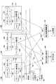
図1は、本発明による一実施形態のロックステップフォルトトレラントコンピュータの構成を示すブロック図である。
【0027】
図1を参照すると、ロックステップフォルトトレラントコンピュータは、コンピューティングモジュール100,200,300、周辺装置制御部400,500、タイミング監視部700、アドレス記憶部701およびデータ転送部702を有する。
【0028】
コンピューティングモジュール100は、プロセッサ101,102、メモリ104およびメモリ制御部105を有している。
【0029】
プロセッサ101とプロセッサ102は同じ構成でありバス103を共有している。プロセッサ101,102のバス103にメモリ制御部105が接続されている。メモリ104はメモリ制御部105に接続されている。
【0030】
メモリ制御部105は信号線730を介してデータ転送部702に接続されている。また、メモリ制御部105は信号線600を介して周辺装置制御部400に接続され、信号線610を介して周辺装置制御部500に接続されている。
【0031】
コンピューティングモジュール100,200,300は全て同じ構成である。コンピューティングモジュール200は、プロセッサ201,202、メモリ204およびメモリ制御部205を有している。プロセッサ201,202はバス203を共有している。メモリ制御部205は信号線731を介してデータ転送部702に接続されている。また、メモリ制御部205は信号線601を介して周辺装置制御部400に接続され、信号線611を介して周辺装置制御部500に接続されている。
【0032】
コンピューティングモジュール300は、プロセッサ301,302、メモリ304およびメモリ制御部305を有している。プロセッサ301,302はバス303を共有している。メモリ制御部305は信号線732を介してデータ転送部702に接続されている。また、メモリ制御部305は信号線602を介して周辺装置制御部400に接続され、信号線612を介して周辺装置制御部500に接続されている。
【0033】
以下、コンピューティングモジュール100に着目して説明する。
【0034】
プロセッサ101,102はロックステップフォルトトレラントコンピュータに与えられた命令を実行する。プロセッサ101,102は他のコンピューティングモジュール200,300のプロセッサとクロック同期して同じ命令を同時に実行する。命令列を実行するとき、プロセッサ101,102は、メモリ制御部105を介してメモリ104にライトアクセスまたはリードアクセスを行う。
【0035】
また、プロセッサ101,102は他のコンピューティングモジュール200,300のプロセッサとクロック同期して周辺装置へアクセスする。周辺装置制御部400に接続された周辺装置へのアクセスは、バス103、メモリ制御部105および信号線600を介して行われる。周辺装置制御部500に接続された周辺装置へのアクセスは、バス103、メモリ制御部105および信号線610を介して行われる。
【0036】
また、プロセッサ101,102は、タイミング監視部700からの割り込みにより停止指示を受けると、割り込みが発生したときに処理していたプロセスのコンテキストを所定のメモリ領域に掃き出して停止する。さらに、プロセッサ101,102は、自身のロックステップが外れたことによる停止指示により停止すると、その後にハードウェア診断を実行する。ハードウェア診断とは、コンピューティングモジュール100内のハードウェアに故障があるか否か診断するものである。
【0037】
メモリ制御部105は、プロセッサ101,102からのライトアクセスおよびリードアクセスのリクエストをメモリ104に伝える。また、メモリ制御部105は、メモリからのレスポンスをプロセッサ101,102に伝える。
【0038】
リクエストはライトアクセスまたはリードアクセスのときにプロセッサからメモリに送られる。ライトアクセスのリクエストには書き込みデータが含まれる。また、レスポンスはリードアクセスのときにメモリからプロセッサに送られる。レスポンスには読出しデータが含まれる。
【0039】
また、メモリ制御部105は、プロセッサ101,102から各周辺装置へのアクセスを周辺装置制御部400,500に伝える。
【0040】
また、メモリ制御部105は、データ転送部702から信号線730を介したアクセスをメモリ104に伝える。一例として、データ転送部702からのアクセスはDMA転送を行うものである。DMA転送では、メモリ104がデータ転送元になる場合と、データ転送先になる場合がある。
【0041】
周辺装置制御部400,500は、全てのコンピューティングモジュール100,200,300からの周辺装置へのアクセスのリクエストが一致しているか否か監視している。全てのコンピューティングモジュール100,200,300からのリクエストが一致していれば、周辺装置制御部400,500はそれらを1つのリクエストとして周辺装置に伝える。それらのリクエストが一致していなければ、周辺装置制御部400,500は、例えば、それらのリクエストを破棄してもよく、また多数決によって定まるリクエストを周辺装置に伝えてもよい。
【0042】
また、周辺装置へのアクセスがリードアクセスの場合、周辺装置制御部400,500は周辺装置から読み出されたデータを含むレスポンスを全てのコンピューティングモジュール100,200,300に同じタイミングで伝える。
【0043】
タイミング監視部700は、信号線710および信号線720を介して、コンピューティングモジュール100のバス103に接続されている。信号線710は、プロセッサ101,102からメモリ104または周辺装置へのアクセスのリクエストにおいて、アドレスの出力タイミングを示すアドレスストローブをバス103からタイミング監視部700に伝える。信号線720は、プロセッサ101,102からメモリ104または周辺装置へのアクセスのリクエストにおいて、コマンドおよびアドレスをパス103からタイミング監視部700に伝える。コマンドとは、例えばライトアクセスかリードアクセスかなどである。
【0044】
タイミング監視部700は、同様に、信号線711および信号線721を介して、コンピューティングモジュール200のバス203に接続されており、信号線712および信号線722を介して、コンピューティングモジュール300のバス303に接続されている。
【0045】
タイミング監視部700は、信号線710,711,712を介して受信したアドレスストローブと、信号線720,721,722を介して受信したコマンドおよびアドレスとを用いて、各コンピューティングモジュール100,200,300のアクセスが一致するか否か監視する。アクセスの不一致を検出すると、タイミング監視部700は、アクセスの不一致と、不一致となったコンピューティングモジュールをアドレス記憶部701に通知する。
【0046】
アクセスが不一致となったコンピューティングモジュールはロックステップの外れたものと判断される。
【0047】
また、タイミング監視部700は、アクセスの不一致を検出すると、全てのコンピューティングモジュールのプロセッサに割り込みによって停止指示を通知する。これにより、各プロセッサは、割り込みが発生したときに処理していたプロセスのコンテキストを所定のメモリ領域に掃き出して停止する。
【0048】
アクセスの一致の監視の具体例としては、タイミング監視部700は、各コンピューティングモジュール100,200,300から同じサイクルでアドレスストローブが受信され、かつ、そのタイミングで受信されたコマンドおよびアドレスが同じであれば、アクセスが一致したと判断すればよい。より簡易的な具体例として、タイミング監視部700は、アドレスストローブのみを受信し、各コンピューティングモジュール100,200,300から同じサイクルでアドレスストローブが受信されればアクセスが一致したと判断してもよい。
【0049】
アドレス記憶部701は、ロックステップの外れたコンピューティングモジュール内のメモリに記録されたデータがロックステップの外れていないコンピューティングモジュール内のメモリに記録されたデータと異なるアドレスを保持するバッファを有している。
【0050】
アドレス記憶部701は、アクセスの不一致と、不一致の検出されたコンピューティングモジュールをタイミング監視部701から通知されると、不一致が検出されたアクセスおよびそれ以降の各コンピューティングモジュールによるライトアクセスについて、アクセスされたアドレスを記録する。
【0051】
データ転送部702は、全てのコンピューティングモジュールのプロセッサが停止し、その後に行われるハードウェア診断が完了すると、エラーインディケータフラグとハードウェア診断の結果とを確認する。エラーインディケータフラグは、コンピューティングモジュール内にエラーが発生していることを示すフラグである。固定的な故障が発生していれば、データ転送部702はエラーインディケータフラグまたはハードウェア診断結果からそれを知ることができる。
【0052】
コンピューティングモジュール内に固定的な故障が発生していなければ、データ転送部702は、ロックステップの外れたコンピューティングモジュールのメモリの内容を他のコンピューティングモジュールのメモリの内容と一致させる再同期化処理を行う。
【0053】
コンピューティングモジュールにキャッシュがあれば、再同期化処理において、ロックステップの外れていないコンピューティングモジュールにおいてキャッシュフラッシュが実行される。キャッシュフラッシュが実行されるのは、ロックステップの外れていないいずれか1つのコンピューティングモジュールであってもよい。
【0054】
このキャッシュフラッシュによりキャッシュ内のデータがメモリに掃き出される。このとき、データがライトされたメモリのアドレスはアドレス記憶部701に記録される。
【0055】
キャッシュフラッシュが完了すると、データ転送部702は、アドレス記憶部701に記録さているアドレスについて、ロックステップの外れていないコンピューティングモジュールのメモリからロックステップの外れたコンピューティングモジュールのメモリにデータをコピーする。このとき、データのコピーにはDMA転送が用いられてもよい。
【0056】
データ転送部702はデータのコピーを完了すると、全てのコンピューティングモジュールをリセットし、通常運用を開始させる。このとき、全てのコンピューティングモジュールのプロセッサは、コンピューティングモジュールの所定のメモリ領域にあるコンテキストを使って通常運用時の動作を開始する。
【0057】
なお、本実施形態では、プロセッサ101,102からメモリ104へのアクセスのリクエストはバス103から引き出した信号線710,720によりタイミング監視部700およびアドレス記憶部701に伝えられている。しかし、本発明はこれに限定されるものではない。例えば、信号線710,720はメモリ制御部105とメモリ104の間の信号線から引き出されてもよい。
【0058】
本実施形態のロックステップフォルトトレラントコンピュータの動作の流れについて説明する。
【0059】
通常、コンピューティングモジュール100,200,300はクロック同期して、ロックステップフォルトトレラントコンピュータに与えられた同じ命令列を同時に実行している。各コンピューティングモジュール100,200,300のプロセッサは命令に従ってメモリや周辺装置にアクセスする。コンピューティングモジュール100,200,300のアクセスは、タイミング、コマンドおよびアドレスが一致しているか否かタイミング監視部700により監視されている。
【0060】
ここで、コンピューティングモジュール100に擾乱が入り、コンピューティングモジュール100のアクセスが他のコンピューティングモジュール200,300のアクセスと不一致になったとする。ただし、コンピューティングモジュール100に固定的な故障は生じていないものとする。
【0061】
その不一致はタイミング監視部700により検出される。その不一致を検出すると、タイミング監視部700は、コンピューティングモジュール100のロックステップが外れたと判断し、アクセスの不一致および不一致となったコンピューティングモジュールをアドレス記憶部701に通知する。
【0062】
また、タイミング監視部700は、全てのコンピューティングモジュールのプロセッサに対して割り込みによって停止指示を通知する。
【0063】
アクセスの不一致と、不一致となったコンピューティングモジュール100を通知されると、アドレス記憶部701は、不一致が検出したアクセスおよびそれ以降の、各コンピューティングによるライトアクセスについて、アクセスされたアドレスを記録する。
【0064】
停止指示を受けたプロセッサは、処理中のプロセスのコンテキストを所定のメモリ領域に掃き出して停止する。
【0065】
アクセスが他のコンピューティングモジュールと不一致となったコンピューティングモジュール(ここではコンピューティングモジュール100)については、その後、ハードウェア診断が実行される。
【0066】
ハードウェア診断が完了すると、データ転送部702がエラーインディケータとハードウェア診断の結果を確認する。ここでは、コンピューティングモジュール100には固定的な故障が生じていないので、データ転送部702は再同期化処理を行う。
【0067】
再同期化処理においては、ロックステップの外れていないコンピューティングモジュールにキャッシュがあれば、キャッシュフラッシュが行われる。このキャッシュフラッシュによりキャッシュ内のデータがメモリに掃き出される。メモリに対するデータの掃き出しはライトアクセスにより行われるので、データの掃き出されたアドレスはアドレス記憶部701に記録される。
【0068】
次に、データ転送部702は、アドレス記憶部701に記録さているアドレスについのみ、再同期化するコンピューティングモジュール(ここではコンピューティングモジュール100)に対して他のコンピューティングモジュールのデータをコピーする。このデータコピーはDMA転送により行われる。
【0069】
通常、アドレス記憶部701に記憶されているアドレスの数は、全体のアドレス数に比べて非常に少ない数である。そのため、ここでのデータコピーは全アドレスのデータコピーに比べて非常に短い時間で終了する。
【0070】
データコピーを完了すると、データ転送部702は全コンピューティングモジュールをリセットする。リセットされると、全てのコンピューティングモジュール100,200,300は互いにクロック同期し、通常の運用を開始する。
【0071】
以上説明したように、本実施形態によれば、タイミング監視部700が、ロックステップの外れを検出すると、アドレス記憶部701が、ロックステップの外れたコンピューティングモジュールにおいてデータが他のコンピューティングモジュールと異なる可能性のあるメモリのアドレスを記録し、再同期化するとき、データ転送部702が、アドレス記憶部701に記録されているアドレスのデータだけをDMA転送によりコピーするので、ロックステップを早期に検出可能であるとともに短い時間でデータコピーが完了させることができ、固定的な故障でない要因によりロックステップの外れたコンピューティングモジュールを早期に運用に組み込むことができる。
【0072】
なお、本実施形態では、ロックステップフォルトトレラントコンピュータが3つのコンピューティングモジュール100,200,300を有する構成を例示したが、本発明はそれに限定されない。コンピューティングモジュールは複数であればよい。
【0073】
【発明の効果】
本発明の情報処理装置によれば、監視手段がロックステップの外れを検出すると、アドレス記憶手段が、ロックステップの外れたモジュールにおいてデータが他のモジュールと異なる可能性のあるメモリのアドレスを記録し、データコピー手段が、アドレス記憶手段に記録されているアドレスのデータだけをコピーするので、短い時間でデータコピーが完了させることができ、ロックステップの外れたモジュールを早期に運用に組み込むことができる。また、本発明によれば、ロックステップを早期に検出することができる。
【図面の簡単な説明】
【図1】本発明による一実施形態のロックステップフォルトトレラントコンピュータの構成を示すブロック図である。
【符号の説明】
100,200,300 コンピューティングモジュール
101,102,201,202,301,302 プロセッサ
103,203,303 バス
104,204,304 メモリ
105,205,305 メモリ制御部
400,500 周辺装置制御部
600,601,602,610,611,612,710,711,712,730,731,732 信号線
700 タイミング監視部
701 アドレス記憶部
702 データ転送部[0001]
TECHNICAL FIELD OF THE INVENTION
The present invention relates to a fault-tolerant computer such as a lock-step fault-tolerant computer that simultaneously processes the same instruction sequence by a plurality of clock-synchronized computing modules, and in particular, the operation of other computing modules is not identical. The present invention relates to speeding up processing for synchronizing a computing module separated from operation with another computing module.
[0002]
[Prior art]
A conventional lockstep fault-tolerant computer has a plurality of computing modules, and the plurality of computing modules execute the same instruction simultaneously. Then, one of the computing modules may operate differently from the other computing modules due to a failure or some other factor.
[0003]
When a lockstep fault-tolerant computer detects a computing module that behaves differently from other computing modules (ie, loses lockstep), it temporarily disconnects the computing module from operation.
[0004]
There are various factors that cause the lock step of the computing module to go off. Then, a method of coping with the departure of the lock step differs depending on factors.
[0005]
One cause of the lockstep loss is a fixed failure that occurs in the computing module. A fixed failure is not a temporary disturbance or a failure that naturally recovers, but one that requires some kind of repair.
[0006]
When a permanent failure of any computing module occurs, the failed computing module is typically removed from the lockstep fault-tolerant computer and replaced with another healthy computing module.
[0007]
Another factor that may cause the lockstep to deviate may be that the operation timing is temporarily shifted from the other computing modules due to a difference in the manufacturing of the computing module. Further, as another factor, it is conceivable that the memory temporarily malfunctions due to the influence of α-rays or the like. In these cases, there is no need to replace the computing module because no permanent failure has occurred in the computing module.
[0008]
If a fixed failure occurs, the computing module is replaced.If the fixed failure does not occur, the computing module that has been disconnected from the operation state is not replaced and replaced with another computing module. Synchronize with the switching module. The process of synchronizing (incorporating into the operation) a computing module disconnected from operation with another computing module is called resynchronization processing.
[0009]
When incorporating a computing module that has been disconnected from its operational state, the lockstep fault-tolerant computer copies the contents of the memory of the other computing module to the memory of the computing module that performs the integration. Thereafter, the newly incorporated computing module operates the same as the other computing modules.
[0010]
[Problems to be solved by the invention]
In a conventional lock-step fault-tolerant computer, when a computing module separated from an operation state is installed, all the computing modules are stopped and the entire contents of the memory are copied. This is to completely match the internal states of all the computing modules.
[0011]
However, in order to improve processing performance and storage capacity, the memory capacity in a computing module of a lock-step fault-tolerant computer has recently increased. At present, the capacity of the memory in the computing module reaches several gigabytes. Therefore, it takes a long time to copy all the contents of the memory in the computing module.
[0012]
Therefore, the conventional lock-step fault-tolerant computer has been suspended for a long time in order to incorporate a computing module separated from the operational state.
[0013]
SUMMARY OF THE INVENTION It is an object of the present invention to provide a fault-tolerant computer with a short downtime when installing a computing module that has been separated from the operation state.
[0014]
[Means for Solving the Problems]
In order to achieve the above object, an information processing device of the present invention includes a plurality of modules each including a processor and a memory,
Monitoring means for monitoring the matching of the operations of the processors of the plurality of modules, and when detecting a module whose operation does not match the processors of the other modules, instructs all the modules to stop,
When the monitoring unit detects that the operation of the processor of one of the modules does not match the operation of another module, the access unit detects the mismatch and detects the address to which the processor of each of the modules performs a write access thereafter. Address storage means for recording;
When all of the modules are stopped, only the addresses recorded in the address storage unit are stored in the memory in the module in which the operation has become inconsistent with the other modules. Has data copying means for copying data from the memory.
[0015]
Therefore, according to the present invention, when the monitoring means detects that the lock step has been lost, the address storage means records the address of the memory where the data may be different from that of another module in the module which has lost the lock step, and Since the copy unit copies only the data at the address recorded in the address storage unit, the data copy can be completed in a short time, and the module out of the lock step can be incorporated into the operation at an early stage.
[0016]
Further, in the information processing apparatus according to the present invention, the data copying unit may copy data only when a fixed failure has not occurred in the module detected by the monitoring unit to be inconsistent with another module. You may copy it.
[0017]
According to one aspect of the present invention, the data copy unit copies data by direct memory access.
[0018]
Further, the information processing apparatus of the present invention is a lock-step type fault-tolerant computer in which the plurality of modules are simultaneously executing the same processing in synchronization with each other with a clock,
The monitoring means may monitor the coincidence of the operations of the processors based on the coincidence of the address strobe timing of the access of each module by the processor.
[0019]
Alternatively, the monitoring means may monitor the timing of the address strobe of the access by the processor of each module, and the matching of the operation of the processor based on the matching of the command and the address at the timing.
[0020]
Therefore, according to the present invention, the lock step can be detected early.
[0021]
According to one aspect of the invention, the processor has a cache,
After all the modules are stopped by the instruction of the monitoring unit, before the data copying unit copies the data, the processor of the module that is not out of lockstep performs cache flush,
The address storage unit records an address to which data is written back by the cache flash.
[0022]
Further, in the information processing apparatus according to the present invention, when the data copy unit completes copying data for all addresses recorded in the address storage unit, all the modules may start operating.
[0023]
BEST MODE FOR CARRYING OUT THE INVENTION
As described in the related art, factors that cause the lock step to be lost include a fixed failure of the computing module and a non-fixed failure. Computing modules that have a fixed failure need to be replaced. However, a computing module that is out of lockstep due to a factor other than a fixed failure is usually incorporated into operation without replacement. Therefore, when the lock step of the computing module is released, the computing module is often installed without being replaced. Further, it is conceivable that the data in the memory of the computing module whose lock step has not been released differs from the data in the memory of another computing module whose lock step has not been released. However, the difference is often small.
[0024]
An embodiment of the present invention will be described in detail with reference to the drawings.
[0025]
The present embodiment is intended to reduce the downtime of a lockstep fault-tolerant computer when a computing module that has been out of lockstep is installed without replacement.
[0026]
FIG. 1 is a block diagram showing the configuration of a lockstep fault-tolerant computer according to an embodiment of the present invention.
[0027]
Referring to FIG. 1, the lockstep fault-tolerant computer includes
[0028]
The
[0029]
The
[0030]
The
[0031]
The
[0032]
The
[0033]
The following description focuses on the
[0034]
[0035]
Further, the
[0036]
Further, when receiving a stop instruction by an interrupt from the
[0037]
The
[0038]
The request is sent from the processor to the memory at the time of write access or read access. The write access request includes write data. The response is sent from the memory to the processor at the time of read access. The response includes the read data.
[0039]
Further, the
[0040]
Further, the
[0041]
The peripheral
[0042]
When the access to the peripheral device is a read access, the peripheral
[0043]
The
[0044]
The
[0045]
The
[0046]
The computing module for which the access does not match is determined to be out of lockstep.
[0047]
Further, when detecting the access mismatch, the
[0048]
As a specific example of monitoring access coincidence, the
[0049]
The
[0050]
When notified from the
[0051]
When the processors of all the computing modules are stopped and the hardware diagnosis performed thereafter is completed, the
[0052]
If a fixed failure has not occurred in the computing module, the
[0053]
If the computing module has a cache, in the resynchronization process, a cache flush is performed on the computing module that is not out of lockstep. A cache flush may be performed on any one computing module that is not out of lockstep.
[0054]
This cache flush causes the data in the cache to be flushed to the memory. At this time, the address of the memory to which the data has been written is recorded in the
[0055]
When the cache flush is completed, the
[0056]
When the
[0057]
In the present embodiment, a request for access to the
[0058]
An operation flow of the lock step fault tolerant computer of the present embodiment will be described.
[0059]
Usually, the
[0060]
Here, it is assumed that disturbance occurs in the
[0061]
The mismatch is detected by the
[0062]
Further, the
[0063]
When notified of the access mismatch and the
[0064]
Upon receiving the stop instruction, the processor sweeps the context of the process being processed to a predetermined memory area and stops.
[0065]
For a computing module whose access has become inconsistent with another computing module (here, computing module 100), a hardware diagnosis is then performed.
[0066]
When the hardware diagnosis is completed, the
[0067]
In the resynchronization process, if there is a cache in a computing module that is not out of lockstep, a cache flush is performed. This cache flush causes the data in the cache to be flushed to the memory. Since the flushing of data to the memory is performed by the write access, the flushed address of the data is recorded in the
[0068]
Next, the
[0069]
Usually, the number of addresses stored in the
[0070]
When the data copy is completed, the
[0071]
As described above, according to the present embodiment, when the
[0072]
Note that, in the present embodiment, a configuration in which the lockstep fault-tolerant computer has three
[0073]
【The invention's effect】
According to the information processing apparatus of the present invention, when the monitoring unit detects the lock step is out, the address storage unit records the address of the memory in which the data in the module out of the lock step may be different from other modules. Since the data copy unit copies only the data at the address recorded in the address storage unit, the data copy can be completed in a short time, and the module out of the lock step can be incorporated into the operation early. . Further, according to the present invention, a lock step can be detected early.
[Brief description of the drawings]
FIG. 1 is a block diagram showing the configuration of a lockstep fault-tolerant computer according to an embodiment of the present invention.
[Explanation of symbols]
100, 200, 300
Claims (7)
Translated fromJapanese複数の前記モジュールのプロセッサの動作の一致を監視しており、他のモジュールのプロセッサと動作が不一致となったモジュールを検出すると、全ての前記モジュールに停止を指示する監視手段と、
前記監視手段により、いずれかのモジュールのプロセッサの動作が他のモジュールと不一致となったことが検出されると、不一致が検出されたアクセスおよびそれ以降に前記各モジュールのプロセッサがライトアクセスするアドレスを記録するアドレス記憶手段と、
全ての前記モジュールが停止すると、動作が他のモジュールと不一致となったことが前記監視手段により検出された前記モジュール内のメモリに、前記アドレス記憶手段に記録されたアドレスについてのみ、他のモジュール内のメモリからデータをコピーするデータコピー手段を有する情報処理装置。A plurality of modules each having a processor and a memory;
Monitoring means for monitoring the matching of the operations of the processors of the plurality of modules, and when detecting a module whose operation does not match the processors of the other modules, instructs all the modules to stop,
When the monitoring unit detects that the operation of the processor of one of the modules does not match the operation of another module, the access unit detects the mismatch and detects the address to which the processor of each of the modules performs a write access thereafter. Address storage means for recording;
When all of the modules are stopped, only the addresses recorded in the address storage unit are stored in the memory in the module in which the operation has become inconsistent with the other modules. An information processing apparatus having data copying means for copying data from a memory.
前記監視手段は、前記各モジュールのプロセッサによるアクセスのアドレスストローブのタイミングの一致により前記プロセッサの動作の一致を監視する、請求項1〜3のいずれか1項に記載の情報処理装置。A plurality of the modules are simultaneously executing the same processing in synchronization with each other, and
4. The information processing apparatus according to claim 1, wherein the monitoring unit monitors a match in operation of the processor based on a match in an address strobe of an access by the processor of each module. 5.
前記監視手段は、前記各モジュールのプロセッサによる、アクセスのアドレスストローブのタイミング、該タイミングにおけるコマンドおよびアドレスの一致により前記プロセッサの動作の一致を監視する、請求項1〜3のいずれか1項に記載の情報処理装置。A plurality of the modules are simultaneously executing the same processing in synchronization with each other, and
4. The monitoring unit according to claim 1, wherein the monitoring unit monitors a timing of an address strobe of an access by a processor of each module, and a match of an operation of the processor based on a match of a command and an address at the timing. 5. Information processing device.
前記監視手段の指示により全ての前記モジュールが停止した後、前記データコピー手段がデータをコピーする前に、ロックステップの外れていないモジュールのプロセッサがキャッシュフラッシュを行い、
前記アドレス記憶手段は、前記キャッシュフラッシュによりデータの書き戻されるアドレスを記録する、請求項1〜5のいずれか1項に記載の情報処理装置。The processor has a cache;
After all the modules are stopped by the instruction of the monitoring unit, before the data copying unit copies the data, the processor of the module that is not out of lockstep performs cache flush,
The information processing apparatus according to claim 1, wherein the address storage unit records an address to which data is written back by the cache flash.
Priority Applications (10)
| Application Number | Priority Date | Filing Date | Title |
|---|---|---|---|
| JP2002201796AJP2004046455A (en) | 2002-07-10 | 2002-07-10 | Information processor |
| TW092118159ATWI241479B (en) | 2002-07-10 | 2003-07-03 | Information processing apparatus |
| CA002434290ACA2434290A1 (en) | 2002-07-10 | 2003-07-04 | Information processing apparatus |
| US10/612,930US20040153731A1 (en) | 2002-07-10 | 2003-07-07 | Information processing apparatus |
| CNB031453627ACN1269040C (en) | 2002-07-10 | 2003-07-08 | Information processor |
| AU2003211183AAU2003211183A1 (en) | 2002-07-10 | 2003-07-08 | Information Processing Apparatus |
| KR1020030046385AKR100566340B1 (en) | 2002-07-10 | 2003-07-09 | Information processing apparatus |
| EP03015794AEP1380950B1 (en) | 2002-07-10 | 2003-07-10 | Fault tolerant information processing apparatus |
| DE60303468TDE60303468T2 (en) | 2002-07-10 | 2003-07-10 | Fault tolerant information processing device |
| ES03015794TES2253613T3 (en) | 2002-07-10 | 2003-07-10 | INFORMATION PROCESSING DEVICE, FAILURE TOLERANT. |
Applications Claiming Priority (1)
| Application Number | Priority Date | Filing Date | Title |
|---|---|---|---|
| JP2002201796AJP2004046455A (en) | 2002-07-10 | 2002-07-10 | Information processor |
Publications (1)
| Publication Number | Publication Date |
|---|---|
| JP2004046455Atrue JP2004046455A (en) | 2004-02-12 |
Family
ID=29728480
Family Applications (1)
| Application Number | Title | Priority Date | Filing Date |
|---|---|---|---|
| JP2002201796APendingJP2004046455A (en) | 2002-07-10 | 2002-07-10 | Information processor |
Country Status (10)
| Country | Link |
|---|---|
| US (1) | US20040153731A1 (en) |
| EP (1) | EP1380950B1 (en) |
| JP (1) | JP2004046455A (en) |
| KR (1) | KR100566340B1 (en) |
| CN (1) | CN1269040C (en) |
| AU (1) | AU2003211183A1 (en) |
| CA (1) | CA2434290A1 (en) |
| DE (1) | DE60303468T2 (en) |
| ES (1) | ES2253613T3 (en) |
| TW (1) | TWI241479B (en) |
Cited By (4)
| Publication number | Priority date | Publication date | Assignee | Title |
|---|---|---|---|---|
| US7493517B2 (en) | 2004-12-17 | 2009-02-17 | Nec Corporation | Fault tolerant computer system and a synchronization method for the same |
| US7500139B2 (en) | 2004-12-21 | 2009-03-03 | Nec Corporation | Securing time for identifying cause of asynchronism in fault-tolerant computer |
| JP2013210796A (en)* | 2012-03-30 | 2013-10-10 | Oki Electric Ind Co Ltd | System and program for constructing redundancy |
| JP2014157492A (en)* | 2013-02-15 | 2014-08-28 | Nec Corp | Fault tolerant server, its memory copy method and memory module for storing write address data |
Families Citing this family (11)
| Publication number | Priority date | Publication date | Assignee | Title |
|---|---|---|---|---|
| US7155721B2 (en)* | 2002-06-28 | 2006-12-26 | Hewlett-Packard Development Company, L.P. | Method and apparatus for communicating information between lock stepped processors |
| US7085959B2 (en)* | 2002-07-03 | 2006-08-01 | Hewlett-Packard Development Company, L.P. | Method and apparatus for recovery from loss of lock step |
| JP2004046599A (en)* | 2002-07-12 | 2004-02-12 | Nec Corp | Fault tolerant computer apparatus, resynchronization method and resynchronization program |
| US7350026B2 (en)* | 2004-12-03 | 2008-03-25 | Thales | Memory based cross compare for cross checked systems |
| JP4117684B2 (en)* | 2004-12-20 | 2008-07-16 | 日本電気株式会社 | Fault-tolerant / duplex computer system and its control method |
| US7730350B2 (en)* | 2005-04-28 | 2010-06-01 | Hewlett-Packard Development Company, L.P. | Method and system of determining the execution point of programs executed in lock step |
| US7496786B2 (en)* | 2006-01-10 | 2009-02-24 | Stratus Technologies Bermuda Ltd. | Systems and methods for maintaining lock step operation |
| TWI397820B (en)* | 2007-03-25 | 2013-06-01 | Mstar Semiconductor Inc | Memory interface device and memory data access method applied thereto |
| US7979746B2 (en)* | 2009-04-27 | 2011-07-12 | Honeywell International Inc. | Dual-dual lockstep processor assemblies and modules |
| CN104516840B (en)* | 2013-09-29 | 2017-08-29 | 联想(北京)有限公司 | Information processing method and message processing device |
| CN112767332B (en)* | 2021-01-08 | 2024-05-17 | 心医国际数字医疗系统(大连)有限公司 | A method and system for determining blood vessel regions based on CTA images |
Family Cites Families (26)
| Publication number | Priority date | Publication date | Assignee | Title |
|---|---|---|---|---|
| US4394745A (en)* | 1980-04-11 | 1983-07-19 | Sony Corporation | Video editing apparatus |
| DE3923872A1 (en)* | 1989-07-19 | 1991-01-24 | Philips Patentverwaltung | CIRCUIT ARRANGEMENT FOR CONTROLLING ACCESS TO A MEMORY |
| JP2836637B2 (en)* | 1990-07-06 | 1998-12-14 | 三菱電機株式会社 | Wireless communication device control device |
| US5249188A (en)* | 1991-08-26 | 1993-09-28 | Ag Communication Systems Corporation | Synchronizing two processors as an integral part of fault detection |
| EP0986007A3 (en)* | 1993-12-01 | 2001-11-07 | Marathon Technologies Corporation | Method of isolating I/O requests |
| FR2737029B1 (en)* | 1995-07-19 | 1997-09-26 | Sextant Avionique | INTERFACE DEVICE BETWEEN A COMPUTER WITH REDUNDANT ARCHITECTURE AND A COMMUNICATION MEANS |
| DE19626184C2 (en)* | 1996-06-29 | 1998-07-30 | Alexander Ernst Erdwin Lahmann | Device for operating a system with two processors which are functionally connected in parallel in a computer |
| US5953742A (en)* | 1996-07-01 | 1999-09-14 | Sun Microsystems, Inc. | Memory management in fault tolerant computer systems utilizing a first and second recording mechanism and a reintegration mechanism |
| US5799022A (en)* | 1996-07-01 | 1998-08-25 | Sun Microsystems, Inc. | Faulty module location in a fault tolerant computer system |
| US5903717A (en)* | 1997-04-02 | 1999-05-11 | General Dynamics Information Systems, Inc. | Fault tolerant computer system |
| US6249828B1 (en)* | 1997-05-13 | 2001-06-19 | Micron Electronics, Inc. | Method for the hot swap of a mass storage adapter on a system including a statically loaded adapter driver |
| US6314525B1 (en)* | 1997-05-13 | 2001-11-06 | 3Com Corporation | Means for allowing two or more network interface controller cards to appear as one card to an operating system |
| US6065102A (en)* | 1997-09-12 | 2000-05-16 | Adaptec, Inc. | Fault tolerant multiple client memory arbitration system capable of operating multiple configuration types |
| CA2309926A1 (en)* | 1997-11-14 | 1999-05-27 | Erik Muench | Method for maintaining the synchronized execution in fault resilient/fault tolerant computer systems |
| US6243829B1 (en)* | 1998-05-27 | 2001-06-05 | Hewlett-Packard Company | Memory controller supporting redundant synchronous memories |
| US6138198A (en)* | 1998-06-15 | 2000-10-24 | Sun Microsystems, Inc. | Processor bridge with dissimilar data registers which is operable to disregard data differences for dissimilar data write accesses |
| US7007190B1 (en)* | 2000-09-06 | 2006-02-28 | Cisco Technology, Inc. | Data replication for redundant network components |
| GB2369692B (en)* | 2000-11-29 | 2002-10-16 | Sun Microsystems Inc | Processor state reintegration |
| US6928583B2 (en)* | 2001-04-11 | 2005-08-09 | Stratus Technologies Bermuda Ltd. | Apparatus and method for two computing elements in a fault-tolerant server to execute instructions in lockstep |
| US6970392B1 (en)* | 2001-06-29 | 2005-11-29 | Cypress Semiconductor Corp. | High speed asynchronous and programmable state machine for generating almost full synchronous flags in a synchronous FIFO |
| US7085955B2 (en)* | 2001-09-14 | 2006-08-01 | Hewlett-Packard Development Company, L.P. | Checkpointing with a write back controller |
| US7472230B2 (en)* | 2001-09-14 | 2008-12-30 | Hewlett-Packard Development Company, L.P. | Preemptive write back controller |
| US20030163769A1 (en)* | 2002-02-27 | 2003-08-28 | Sun Microsystems, Inc. | Memory module including an error detection mechanism for address and control signals |
| US6941493B2 (en)* | 2002-02-27 | 2005-09-06 | Sun Microsystems, Inc. | Memory subsystem including an error detection mechanism for address and control signals |
| US7003692B1 (en)* | 2002-05-24 | 2006-02-21 | Cisco Technology, Inc. | Dynamic configuration synchronization in support of a “hot” standby stateful switchover |
| US7003691B2 (en)* | 2002-06-28 | 2006-02-21 | Hewlett-Packard Development Company, L.P. | Method and apparatus for seeding differences in lock-stepped processors |
- 2002
- 2002-07-10JPJP2002201796Apatent/JP2004046455A/enactivePending
- 2003
- 2003-07-03TWTW092118159Apatent/TWI241479B/ennot_activeIP Right Cessation
- 2003-07-04CACA002434290Apatent/CA2434290A1/ennot_activeAbandoned
- 2003-07-07USUS10/612,930patent/US20040153731A1/ennot_activeAbandoned
- 2003-07-08CNCNB031453627Apatent/CN1269040C/ennot_activeExpired - Fee Related
- 2003-07-08AUAU2003211183Apatent/AU2003211183A1/ennot_activeAbandoned
- 2003-07-09KRKR1020030046385Apatent/KR100566340B1/ennot_activeExpired - Fee Related
- 2003-07-10ESES03015794Tpatent/ES2253613T3/ennot_activeExpired - Lifetime
- 2003-07-10EPEP03015794Apatent/EP1380950B1/ennot_activeExpired - Lifetime
- 2003-07-10DEDE60303468Tpatent/DE60303468T2/ennot_activeExpired - Fee Related
Cited By (4)
| Publication number | Priority date | Publication date | Assignee | Title |
|---|---|---|---|---|
| US7493517B2 (en) | 2004-12-17 | 2009-02-17 | Nec Corporation | Fault tolerant computer system and a synchronization method for the same |
| US7500139B2 (en) | 2004-12-21 | 2009-03-03 | Nec Corporation | Securing time for identifying cause of asynchronism in fault-tolerant computer |
| JP2013210796A (en)* | 2012-03-30 | 2013-10-10 | Oki Electric Ind Co Ltd | System and program for constructing redundancy |
| JP2014157492A (en)* | 2013-02-15 | 2014-08-28 | Nec Corp | Fault tolerant server, its memory copy method and memory module for storing write address data |
Also Published As
| Publication number | Publication date |
|---|---|
| AU2003211183A1 (en) | 2004-01-29 |
| CA2434290A1 (en) | 2004-01-10 |
| DE60303468D1 (en) | 2006-04-20 |
| TW200402622A (en) | 2004-02-16 |
| CN1269040C (en) | 2006-08-09 |
| ES2253613T3 (en) | 2006-06-01 |
| TWI241479B (en) | 2005-10-11 |
| DE60303468T2 (en) | 2006-09-28 |
| KR100566340B1 (en) | 2006-03-31 |
| EP1380950B1 (en) | 2006-02-08 |
| KR20040005684A (en) | 2004-01-16 |
| CN1472650A (en) | 2004-02-04 |
| EP1380950A1 (en) | 2004-01-14 |
| US20040153731A1 (en) | 2004-08-05 |
Similar Documents
| Publication | Publication Date | Title |
|---|---|---|
| US7496786B2 (en) | Systems and methods for maintaining lock step operation | |
| KR101121116B1 (en) | Synchronization control apparatus, information processing apparatus, and synchronization management method | |
| JPH01154241A (en) | Synchronized double computer system | |
| JP2004046455A (en) | Information processor | |
| WO1995034860A1 (en) | Main memory system and checkpointing protocol for fault-tolerant computer system | |
| JPH01154243A (en) | Interface between non failure-proof element and failure-proof system | |
| US6785763B2 (en) | Efficient memory modification tracking with hierarchical dirty indicators | |
| JPH079625B2 (en) | Computer with fault-tolerant capabilities | |
| US7500139B2 (en) | Securing time for identifying cause of asynchronism in fault-tolerant computer | |
| US6961826B2 (en) | Processor state reintegration using bridge direct memory access controller | |
| US6950907B2 (en) | Enhanced protection for memory modification tracking with redundant dirty indicators | |
| WO2010100757A1 (en) | Arithmetic processing system, resynchronization method, and firmware program | |
| JP4161276B2 (en) | Fault-tolerant computer device and synchronization method thereof | |
| JP3774826B2 (en) | Information processing device | |
| US6785777B2 (en) | Control logic for memory modification tracking with hierarchical dirty indicators | |
| US6981172B2 (en) | Protection for memory modification tracking | |
| JPH0916535A (en) | Multiprocessor computer | |
| JPH06348604A (en) | Memory copy system | |
| JPH06124242A (en) | Redundant shared memory equivalence guarantee method |
Legal Events
| Date | Code | Title | Description |
|---|---|---|---|
| A621 | Written request for application examination | Free format text:JAPANESE INTERMEDIATE CODE: A621 Effective date:20040427 | |
| RD03 | Notification of appointment of power of attorney | Free format text:JAPANESE INTERMEDIATE CODE: A7423 Effective date:20041220 | |
| RD04 | Notification of resignation of power of attorney | Free format text:JAPANESE INTERMEDIATE CODE: A7424 Effective date:20041220 | |
| A977 | Report on retrieval | Free format text:JAPANESE INTERMEDIATE CODE: A971007 Effective date:20050622 | |
| A131 | Notification of reasons for refusal | Free format text:JAPANESE INTERMEDIATE CODE: A131 Effective date:20051207 | |
| RD04 | Notification of resignation of power of attorney | Free format text:JAPANESE INTERMEDIATE CODE: A7424 Effective date:20060127 | |
| A521 | Written amendment | Free format text:JAPANESE INTERMEDIATE CODE: A523 Effective date:20060201 | |
| A02 | Decision of refusal | Free format text:JAPANESE INTERMEDIATE CODE: A02 Effective date:20060405 | |
| A521 | Written amendment | Free format text:JAPANESE INTERMEDIATE CODE: A523 Effective date:20060508 | |
| RD01 | Notification of change of attorney | Free format text:JAPANESE INTERMEDIATE CODE: A7421 Effective date:20060508 | |
| A521 | Written amendment | Free format text:JAPANESE INTERMEDIATE CODE: A821 Effective date:20060508 | |
| A911 | Transfer to examiner for re-examination before appeal (zenchi) | Free format text:JAPANESE INTERMEDIATE CODE: A911 Effective date:20060712 | |
| A912 | Re-examination (zenchi) completed and case transferred to appeal board | Free format text:JAPANESE INTERMEDIATE CODE: A912 Effective date:20060825 | |
| RD01 | Notification of change of attorney | Free format text:JAPANESE INTERMEDIATE CODE: A7421 Effective date:20070119 | |
| RD01 | Notification of change of attorney | Free format text:JAPANESE INTERMEDIATE CODE: A7421 Effective date:20080604 | |
| RD01 | Notification of change of attorney | Free format text:JAPANESE INTERMEDIATE CODE: A7421 Effective date:20090508 |