JP2004040110A - Method for depositing a silicon dioxide layer on a substrate by atomic layer deposition - Google Patents
Method for depositing a silicon dioxide layer on a substrate by atomic layer depositionDownload PDFInfo
- Publication number
- JP2004040110A JP2004040110AJP2003271607AJP2003271607AJP2004040110AJP 2004040110 AJP2004040110 AJP 2004040110AJP 2003271607 AJP2003271607 AJP 2003271607AJP 2003271607 AJP2003271607 AJP 2003271607AJP 2004040110 AJP2004040110 AJP 2004040110A
- Authority
- JP
- Japan
- Prior art keywords
- reactant
- catalyst
- chamber
- time length
- immediately
- Prior art date
- Legal status (The legal status is an assumption and is not a legal conclusion. Google has not performed a legal analysis and makes no representation as to the accuracy of the status listed.)
- Granted
Links
Images


Classifications
- C—CHEMISTRY; METALLURGY
- C23—COATING METALLIC MATERIAL; COATING MATERIAL WITH METALLIC MATERIAL; CHEMICAL SURFACE TREATMENT; DIFFUSION TREATMENT OF METALLIC MATERIAL; COATING BY VACUUM EVAPORATION, BY SPUTTERING, BY ION IMPLANTATION OR BY CHEMICAL VAPOUR DEPOSITION, IN GENERAL; INHIBITING CORROSION OF METALLIC MATERIAL OR INCRUSTATION IN GENERAL
- C23C—COATING METALLIC MATERIAL; COATING MATERIAL WITH METALLIC MATERIAL; SURFACE TREATMENT OF METALLIC MATERIAL BY DIFFUSION INTO THE SURFACE, BY CHEMICAL CONVERSION OR SUBSTITUTION; COATING BY VACUUM EVAPORATION, BY SPUTTERING, BY ION IMPLANTATION OR BY CHEMICAL VAPOUR DEPOSITION, IN GENERAL
- C23C16/00—Chemical coating by decomposition of gaseous compounds, without leaving reaction products of surface material in the coating, i.e. chemical vapour deposition [CVD] processes
- C23C16/22—Chemical coating by decomposition of gaseous compounds, without leaving reaction products of surface material in the coating, i.e. chemical vapour deposition [CVD] processes characterised by the deposition of inorganic material, other than metallic material
- C23C16/30—Deposition of compounds, mixtures or solid solutions, e.g. borides, carbides, nitrides
- C23C16/40—Oxides
- C23C16/401—Oxides containing silicon
- C23C16/402—Silicon dioxide
- C—CHEMISTRY; METALLURGY
- C23—COATING METALLIC MATERIAL; COATING MATERIAL WITH METALLIC MATERIAL; CHEMICAL SURFACE TREATMENT; DIFFUSION TREATMENT OF METALLIC MATERIAL; COATING BY VACUUM EVAPORATION, BY SPUTTERING, BY ION IMPLANTATION OR BY CHEMICAL VAPOUR DEPOSITION, IN GENERAL; INHIBITING CORROSION OF METALLIC MATERIAL OR INCRUSTATION IN GENERAL
- C23C—COATING METALLIC MATERIAL; COATING MATERIAL WITH METALLIC MATERIAL; SURFACE TREATMENT OF METALLIC MATERIAL BY DIFFUSION INTO THE SURFACE, BY CHEMICAL CONVERSION OR SUBSTITUTION; COATING BY VACUUM EVAPORATION, BY SPUTTERING, BY ION IMPLANTATION OR BY CHEMICAL VAPOUR DEPOSITION, IN GENERAL
- C23C16/00—Chemical coating by decomposition of gaseous compounds, without leaving reaction products of surface material in the coating, i.e. chemical vapour deposition [CVD] processes
- C23C16/44—Chemical coating by decomposition of gaseous compounds, without leaving reaction products of surface material in the coating, i.e. chemical vapour deposition [CVD] processes characterised by the method of coating
- C23C16/455—Chemical coating by decomposition of gaseous compounds, without leaving reaction products of surface material in the coating, i.e. chemical vapour deposition [CVD] processes characterised by the method of coating characterised by the method used for introducing gases into reaction chamber or for modifying gas flows in reaction chamber
- C23C16/45523—Pulsed gas flow or change of composition over time
- C23C16/45525—Atomic layer deposition [ALD]
- C23C16/45527—Atomic layer deposition [ALD] characterized by the ALD cycle, e.g. different flows or temperatures during half-reactions, unusual pulsing sequence, use of precursor mixtures or auxiliary reactants or activations
- C23C16/45534—Use of auxiliary reactants other than used for contributing to the composition of the main film, e.g. catalysts, activators or scavengers
- C—CHEMISTRY; METALLURGY
- C23—COATING METALLIC MATERIAL; COATING MATERIAL WITH METALLIC MATERIAL; CHEMICAL SURFACE TREATMENT; DIFFUSION TREATMENT OF METALLIC MATERIAL; COATING BY VACUUM EVAPORATION, BY SPUTTERING, BY ION IMPLANTATION OR BY CHEMICAL VAPOUR DEPOSITION, IN GENERAL; INHIBITING CORROSION OF METALLIC MATERIAL OR INCRUSTATION IN GENERAL
- C23C—COATING METALLIC MATERIAL; COATING MATERIAL WITH METALLIC MATERIAL; SURFACE TREATMENT OF METALLIC MATERIAL BY DIFFUSION INTO THE SURFACE, BY CHEMICAL CONVERSION OR SUBSTITUTION; COATING BY VACUUM EVAPORATION, BY SPUTTERING, BY ION IMPLANTATION OR BY CHEMICAL VAPOUR DEPOSITION, IN GENERAL
- C23C16/00—Chemical coating by decomposition of gaseous compounds, without leaving reaction products of surface material in the coating, i.e. chemical vapour deposition [CVD] processes
- C23C16/56—After-treatment
- H—ELECTRICITY
- H01—ELECTRIC ELEMENTS
- H01L—SEMICONDUCTOR DEVICES NOT COVERED BY CLASS H10
- H01L21/00—Processes or apparatus adapted for the manufacture or treatment of semiconductor or solid state devices or of parts thereof
- H01L21/02—Manufacture or treatment of semiconductor devices or of parts thereof
- H01L21/02104—Forming layers
- H01L21/02107—Forming insulating materials on a substrate
- H01L21/02109—Forming insulating materials on a substrate characterised by the type of layer, e.g. type of material, porous/non-porous, pre-cursors, mixtures or laminates
- H01L21/02205—Forming insulating materials on a substrate characterised by the type of layer, e.g. type of material, porous/non-porous, pre-cursors, mixtures or laminates the layer being characterised by the precursor material for deposition
- H01L21/02208—Forming insulating materials on a substrate characterised by the type of layer, e.g. type of material, porous/non-porous, pre-cursors, mixtures or laminates the layer being characterised by the precursor material for deposition the precursor containing a compound comprising Si
- H—ELECTRICITY
- H01—ELECTRIC ELEMENTS
- H01L—SEMICONDUCTOR DEVICES NOT COVERED BY CLASS H10
- H01L21/00—Processes or apparatus adapted for the manufacture or treatment of semiconductor or solid state devices or of parts thereof
- H01L21/02—Manufacture or treatment of semiconductor devices or of parts thereof
- H01L21/02104—Forming layers
- H01L21/02107—Forming insulating materials on a substrate
- H01L21/02225—Forming insulating materials on a substrate characterised by the process for the formation of the insulating layer
- H01L21/0226—Forming insulating materials on a substrate characterised by the process for the formation of the insulating layer formation by a deposition process
- H01L21/02263—Forming insulating materials on a substrate characterised by the process for the formation of the insulating layer formation by a deposition process deposition from the gas or vapour phase
- H01L21/02271—Forming insulating materials on a substrate characterised by the process for the formation of the insulating layer formation by a deposition process deposition from the gas or vapour phase deposition by decomposition or reaction of gaseous or vapour phase compounds, i.e. chemical vapour deposition
- H01L21/02277—Forming insulating materials on a substrate characterised by the process for the formation of the insulating layer formation by a deposition process deposition from the gas or vapour phase deposition by decomposition or reaction of gaseous or vapour phase compounds, i.e. chemical vapour deposition the reactions being activated by other means than plasma or thermal, e.g. photo-CVD
- H—ELECTRICITY
- H01—ELECTRIC ELEMENTS
- H01L—SEMICONDUCTOR DEVICES NOT COVERED BY CLASS H10
- H01L21/00—Processes or apparatus adapted for the manufacture or treatment of semiconductor or solid state devices or of parts thereof
- H01L21/02—Manufacture or treatment of semiconductor devices or of parts thereof
- H01L21/02104—Forming layers
- H01L21/02107—Forming insulating materials on a substrate
- H01L21/02296—Forming insulating materials on a substrate characterised by the treatment performed before or after the formation of the layer
- H01L21/02318—Forming insulating materials on a substrate characterised by the treatment performed before or after the formation of the layer post-treatment
- H01L21/02337—Forming insulating materials on a substrate characterised by the treatment performed before or after the formation of the layer post-treatment treatment by exposure to a gas or vapour
- H01L21/0234—Forming insulating materials on a substrate characterised by the treatment performed before or after the formation of the layer post-treatment treatment by exposure to a gas or vapour treatment by exposure to a plasma
- H—ELECTRICITY
- H01—ELECTRIC ELEMENTS
- H01L—SEMICONDUCTOR DEVICES NOT COVERED BY CLASS H10
- H01L21/00—Processes or apparatus adapted for the manufacture or treatment of semiconductor or solid state devices or of parts thereof
- H01L21/02—Manufacture or treatment of semiconductor devices or of parts thereof
- H01L21/02104—Forming layers
- H01L21/02107—Forming insulating materials on a substrate
- H01L21/02109—Forming insulating materials on a substrate characterised by the type of layer, e.g. type of material, porous/non-porous, pre-cursors, mixtures or laminates
- H01L21/02112—Forming insulating materials on a substrate characterised by the type of layer, e.g. type of material, porous/non-porous, pre-cursors, mixtures or laminates characterised by the material of the layer
- H01L21/02123—Forming insulating materials on a substrate characterised by the type of layer, e.g. type of material, porous/non-porous, pre-cursors, mixtures or laminates characterised by the material of the layer the material containing silicon
- H01L21/02164—Forming insulating materials on a substrate characterised by the type of layer, e.g. type of material, porous/non-porous, pre-cursors, mixtures or laminates characterised by the material of the layer the material containing silicon the material being a silicon oxide, e.g. SiO2
- H—ELECTRICITY
- H01—ELECTRIC ELEMENTS
- H01L—SEMICONDUCTOR DEVICES NOT COVERED BY CLASS H10
- H01L21/00—Processes or apparatus adapted for the manufacture or treatment of semiconductor or solid state devices or of parts thereof
- H01L21/02—Manufacture or treatment of semiconductor devices or of parts thereof
- H01L21/02104—Forming layers
- H01L21/02107—Forming insulating materials on a substrate
- H01L21/02109—Forming insulating materials on a substrate characterised by the type of layer, e.g. type of material, porous/non-porous, pre-cursors, mixtures or laminates
- H01L21/02205—Forming insulating materials on a substrate characterised by the type of layer, e.g. type of material, porous/non-porous, pre-cursors, mixtures or laminates the layer being characterised by the precursor material for deposition
- H01L21/02208—Forming insulating materials on a substrate characterised by the type of layer, e.g. type of material, porous/non-porous, pre-cursors, mixtures or laminates the layer being characterised by the precursor material for deposition the precursor containing a compound comprising Si
- H01L21/02211—Forming insulating materials on a substrate characterised by the type of layer, e.g. type of material, porous/non-porous, pre-cursors, mixtures or laminates the layer being characterised by the precursor material for deposition the precursor containing a compound comprising Si the compound being a silane, e.g. disilane, methylsilane or chlorosilane
- H—ELECTRICITY
- H01—ELECTRIC ELEMENTS
- H01L—SEMICONDUCTOR DEVICES NOT COVERED BY CLASS H10
- H01L21/00—Processes or apparatus adapted for the manufacture or treatment of semiconductor or solid state devices or of parts thereof
- H01L21/02—Manufacture or treatment of semiconductor devices or of parts thereof
- H01L21/02104—Forming layers
- H01L21/02107—Forming insulating materials on a substrate
- H01L21/02109—Forming insulating materials on a substrate characterised by the type of layer, e.g. type of material, porous/non-porous, pre-cursors, mixtures or laminates
- H01L21/02205—Forming insulating materials on a substrate characterised by the type of layer, e.g. type of material, porous/non-porous, pre-cursors, mixtures or laminates the layer being characterised by the precursor material for deposition
- H01L21/02208—Forming insulating materials on a substrate characterised by the type of layer, e.g. type of material, porous/non-porous, pre-cursors, mixtures or laminates the layer being characterised by the precursor material for deposition the precursor containing a compound comprising Si
- H01L21/02219—Forming insulating materials on a substrate characterised by the type of layer, e.g. type of material, porous/non-porous, pre-cursors, mixtures or laminates the layer being characterised by the precursor material for deposition the precursor containing a compound comprising Si the compound comprising silicon and nitrogen
- H—ELECTRICITY
- H01—ELECTRIC ELEMENTS
- H01L—SEMICONDUCTOR DEVICES NOT COVERED BY CLASS H10
- H01L21/00—Processes or apparatus adapted for the manufacture or treatment of semiconductor or solid state devices or of parts thereof
- H01L21/02—Manufacture or treatment of semiconductor devices or of parts thereof
- H01L21/02104—Forming layers
- H01L21/02107—Forming insulating materials on a substrate
- H01L21/02225—Forming insulating materials on a substrate characterised by the process for the formation of the insulating layer
- H01L21/0226—Forming insulating materials on a substrate characterised by the process for the formation of the insulating layer formation by a deposition process
- H01L21/02263—Forming insulating materials on a substrate characterised by the process for the formation of the insulating layer formation by a deposition process deposition from the gas or vapour phase
- H01L21/02271—Forming insulating materials on a substrate characterised by the process for the formation of the insulating layer formation by a deposition process deposition from the gas or vapour phase deposition by decomposition or reaction of gaseous or vapour phase compounds, i.e. chemical vapour deposition
- H01L21/02274—Forming insulating materials on a substrate characterised by the process for the formation of the insulating layer formation by a deposition process deposition from the gas or vapour phase deposition by decomposition or reaction of gaseous or vapour phase compounds, i.e. chemical vapour deposition in the presence of a plasma [PECVD]
- H—ELECTRICITY
- H01—ELECTRIC ELEMENTS
- H01L—SEMICONDUCTOR DEVICES NOT COVERED BY CLASS H10
- H01L21/00—Processes or apparatus adapted for the manufacture or treatment of semiconductor or solid state devices or of parts thereof
- H01L21/02—Manufacture or treatment of semiconductor devices or of parts thereof
- H01L21/02104—Forming layers
- H01L21/02107—Forming insulating materials on a substrate
- H01L21/02225—Forming insulating materials on a substrate characterised by the process for the formation of the insulating layer
- H01L21/0226—Forming insulating materials on a substrate characterised by the process for the formation of the insulating layer formation by a deposition process
- H01L21/02263—Forming insulating materials on a substrate characterised by the process for the formation of the insulating layer formation by a deposition process deposition from the gas or vapour phase
- H01L21/02271—Forming insulating materials on a substrate characterised by the process for the formation of the insulating layer formation by a deposition process deposition from the gas or vapour phase deposition by decomposition or reaction of gaseous or vapour phase compounds, i.e. chemical vapour deposition
- H01L21/0228—Forming insulating materials on a substrate characterised by the process for the formation of the insulating layer formation by a deposition process deposition from the gas or vapour phase deposition by decomposition or reaction of gaseous or vapour phase compounds, i.e. chemical vapour deposition deposition by cyclic CVD, e.g. ALD, ALE, pulsed CVD
Landscapes
- Chemical & Material Sciences (AREA)
- Engineering & Computer Science (AREA)
- Physics & Mathematics (AREA)
- Chemical Kinetics & Catalysis (AREA)
- Computer Hardware Design (AREA)
- Power Engineering (AREA)
- Microelectronics & Electronic Packaging (AREA)
- Manufacturing & Machinery (AREA)
- General Physics & Mathematics (AREA)
- Condensed Matter Physics & Semiconductors (AREA)
- Materials Engineering (AREA)
- Organic Chemistry (AREA)
- General Chemical & Material Sciences (AREA)
- Metallurgy (AREA)
- Mechanical Engineering (AREA)
- Plasma & Fusion (AREA)
- Inorganic Chemistry (AREA)
- Chemical Vapour Deposition (AREA)
- Formation Of Insulating Films (AREA)
Abstract
Translated fromJapaneseDescription
Translated fromJapanese本発明は、原子層堆積法を用いて、半導体製造等において基板上に二酸化シリコン層を成長させる方法の改良に関するものである。本発明の方法は、例えば、ゲート酸化膜又は誘電層に適用される二酸化シリコン層の特性全体にわたって極めて精密な制御を容易にするものである。本発明の方法は、半導体製造における、ゲートスペーサ、ゲート酸化膜、シリサイドブロッキング層、ビットラインスペーサ、レベル間誘電層、エッチング停止層、それらに関連する最終製品又は中間製品を製造する際に特に有効である。The present invention relates to an improvement in a method for growing a silicon dioxide layer on a substrate in semiconductor manufacturing or the like by using an atomic layer deposition method. The method of the present invention facilitates very precise control over the properties of, for example, a silicon dioxide layer applied to a gate oxide or dielectric layer. The method of the present invention is particularly useful in the manufacture of gate spacers, gate oxides, silicide blocking layers, bit line spacers, interlevel dielectric layers, etch stop layers, and related end products or intermediate products in semiconductor manufacturing. It is.
半導体装置の製造において、化学的気相堆積法(CVD)、低圧CVD(CVD)、又は、プラズマCVD(PECVD)等の従来の手法によって基板表面上に二酸化シリコン層を形成することがよくある。これらの手法は、比較的低温で良好なステップカバレージを提供すると認識されている。しかしながら、半導体装置の密度を増大すると、装置を構成する各要素の高さが高くなる。結果として、増大するパターン密度変動と対応する均一性の減少とに起因して問題が発生する。In the manufacture of semiconductor devices, a silicon dioxide layer is often formed on a substrate surface by conventional techniques such as chemical vapor deposition (CVD), low pressure CVD (CVD), or plasma CVD (PECVD). These approaches have been recognized as providing good step coverage at relatively low temperatures. However, as the density of the semiconductor device increases, the height of each element constituting the device increases. As a result, problems arise due to increasing pattern density variations and a corresponding decrease in uniformity.
本願に参考文献として組み込まれている米国特許第6,090,442号明細書(以下、「クラウス’442」と称する)に教示されているように、これらの認識されている問題に対する一のアプローチは原子層堆積(ALD)技術である。しかしながら、クラウス’442は、ALD技術の大きな欠点は、表面反応が完了するためには、それらが通常600Kより高い温度と、109L(ここで、1L=10−6Torr sec)より大きな反応物質の照射とを必要とすると教示している。このような高温及び高照射処理は、このような処理の実施の困難性を含む種々の理由のために超薄膜の堆積に対して望ましくはない。One approach to these perceived problems is taught in US Pat. No. 6,090,442 (hereinafter "Klaus'442"), which is incorporated herein by reference. Is an atomic layer deposition (ALD) technique. However, Klaus' 442 states that the major drawback of ALD technology is that for surface reactions to be completed, they are typically at temperatures above 600 K and reacting greater than 109 L (where 1 L = 10−6 Torr sec). It teaches that irradiation of the substance is required. Such high temperature and high irradiation processes are not desirable for ultra-thin film deposition for a variety of reasons, including the difficulty in performing such processes.
クラウス’442ではこのような問題に対する改良アプローチが教示している。クラウス’442では、触媒型二元反応シーケンス化学(catalyzed binary reaction sequence chemistry)を用いて室温で機能化基板上に原子層薄膜を成長される方法を提供している。さらに詳細には、クラウス’442特許によって、室温で実施する2元触媒促進型“半反応”を利用して、2段階原子層堆積(ALD)をOH終端基板上に二酸化シリコン膜を成長させるのに用いることができる。'Klaus' 442 teaches an improved approach to such a problem. Claus' 442 provides a method for growing atomic layer thin films on functionalized substrates at room temperature using catalyzed binary reaction sequence chemistry. More specifically, according to the Claus' 442 patent, two-step atomic layer deposition (ALD) is used to grow a silicon dioxide film on an OH-terminated substrate utilizing a two-catalyst promoted "semi-reaction" performed at room temperature. Can be used.
特定の実施形態では、クラウス’442は“第1の分子前駆体”としてSiCl4を、触媒としてピリジンを用いる。第1に、基板を、例えば、H2Oを用いて“第1の官能基”としてOH−で機能化する。次に、機能化基板を、ルイス塩基又はルイス酸(例えば、ピリジン)である触媒と、成長させる膜の主要要素及び第2の官能基(例えば、SiCl4)を含む第1の分子前駆体とに曝す。クラウス’442に示されているように、第1の“半反応”において、触媒は機能化基板の第1の官能基と反応し;次いで、第1の分子前駆体は(触媒によって活性化された)第1の官能基と反応して、触媒の置換と、基板の第1の官能基と第1の分子前駆体の主要要素との間の結合とを生ずる。合わせると、これらの2つの反応は第1の“半反応”を備え、膜の表面にわたって配置するようになった第2の官能基と膜形成を始める。In certain embodiments, Claus' 442 uses SiCl4 as the “first molecular precursor” and pyridine as the catalyst. First, the substrate is functionalized with OH− as a “first functional group” using, for example, H2 O. Next, the functionalized substrate is treated with a catalyst that is a Lewis base or a Lewis acid (eg, pyridine), a first molecular precursor that includes the key elements of the film to be grown and a second functional group (eg, SiCl4 ) Exposure to As shown in Claus' 442, in the first "half-reaction", the catalyst reacts with the first functional group of the functionalized substrate; then, the first molecular precursor is activated (activated by the catalyst). A) reacting with the first functional group to effect displacement of the catalyst and bonding between the first functional group of the substrate and the primary element of the first molecular precursor. Taken together, these two reactions comprise a first "semi-reaction" and begin film formation with a second functional group adapted to be disposed over the surface of the film.
クラウス’442プロセスにおいてこの点では、過剰な第1の分子前駆体と副産物とが反応チャンバから除去され、部分的に反応した基板を付加した触媒と第2の分子前駆体とに曝される。触媒は、反応することによって膜の表面に沿って曝された第2の官能基を活性化し、第2の分子前駆体と共に、第2の官能基の置換と、第1の分子前駆体の主要要素への結合とを生ずる。第2の分子前駆体は、第1の分子前駆体の主要要素と触媒との間の結合と反応して、触媒の置換と新しく成長した表面層上への第1の官能基の堆積とを生じ、それによって、フル成長/堆積サイクルが完了し、次のサイクルの準備において基板表面を機能化状態に戻す。At this point in the 'Klaus' 442 process, excess first molecular precursor and by-products are removed from the reaction chamber and exposed to the partially reacted substrate added catalyst and second molecular precursor. The catalyst activates the second functional group exposed along the surface of the membrane by reacting and, along with the second molecular precursor, displaces the second functional group and the primary molecular precursor. To the element. The second molecular precursor reacts with the bond between the main element of the first molecular precursor and the catalyst to effect the replacement of the catalyst and the deposition of the first functional group on the newly grown surface layer. Occurs, thereby completing the full growth / deposition cycle and returning the substrate surface to a functionalized state in preparation for the next cycle.
クラウス’442特許の触媒補助堆積プロセスはALD技術の実質的な進歩を示すものであり、室温ALDを可能にするものではあるが、クラウス’442技術を用いて成長させた薄膜の表面密度、均一性及び品質は半導体産業において要求された標準には合致しないことがわかった。より小型のマイクロエレクトロニクスコンポーネントへの終わりなき進歩によって、半導体装置の特性にわたってより精密な制御が必要となる。このような精密な制御は、より均一な表面特性及びパターン密度を必要とする。本発明のALD技術の新たな進歩は、従来技術より優れた表面密度とより均一な表面特性とを有する半導体装置用の薄膜を生成し、その結果、薄膜層の特性全般にわたる顕著に精密な制御と、現在の小型化に適したより高品質な半導体装置の製造とが可能となる。Although the catalyst-assisted deposition process of the Klaus '442 patent represents a substantial advance in ALD technology and enables room temperature ALD, the surface density, uniformity, and uniformity of thin films grown using Klaus' 442 technology It has been found that the properties and quality do not meet the standards required in the semiconductor industry. The endless advance to smaller microelectronic components requires more precise control over the characteristics of semiconductor devices. Such precise control requires more uniform surface properties and pattern densities. A new advance in the ALD technology of the present invention is the creation of thin films for semiconductor devices having better surface density and more uniform surface properties than the prior art, resulting in significantly more precise control over the properties of the thin film layers. Thus, it is possible to manufacture a higher-quality semiconductor device suitable for the current miniaturization.
クラウス’442特許は、“トリエチルアミン((C2H5)3N)のような強いアミン塩基は、クロロシランの存在下で塩化トリエチルアンモニウム(NH+(C2H5)3Cl−)のような塩化合物を形成することを示した”旨記載している。この塩は表面を害し、この塩が成長するので反応効率を劣化する(カラム9、24〜28行)。従って、クラウス’442は、ALDの適用において、トリエチルアミン、すなわち第三脂肪族アミンの存在から離れる方向で教示している。Klaus' 442 patent, "salts such as triethylamine strong amine base, such as((C 2 H 5) 3 N) , the triethylammonium chloride in the presence of chlorosilane(NH + (C 2 H 5 ) 3 Cl-) The compound is shown to form a compound. " The salt harms the surface and the reaction grows as the salt grows (column 9, lines 24-28). Thus, Claus' 442 teaches away from the presence of triethylamine, a tertiary aliphatic amine, in ALD applications.
従って、本発明の目的は、良好な表面密度、極めて高い純度を有し、表面特性を高精度で制御された非常に均一な薄膜を成長するために、原子層堆積法(ALD)を用いた方法を提供することである。Therefore, the object of the present invention was to use atomic layer deposition (ALD) to grow very uniform thin films with good surface density, extremely high purity and with controlled surface properties with high precision. Is to provide a way.
本発明の他の目的は、反応物材料の一つとして少なくとも2つのシリコン原子を有するシリコン化合物を用いて半導体基板上に二酸化シリコン層を形成するALD法を提供することである。Another object of the present invention is to provide an ALD method for forming a silicon dioxide layer on a semiconductor substrate using a silicon compound having at least two silicon atoms as one of the reactant materials.
本発明のさらに他の目的は、触媒材料として第三脂肪族アミン化合物を用いて半導体基板上に二酸化シリコン層を形成するALD法を提供することである。Another object of the present invention is to provide an ALD method for forming a silicon dioxide layer on a semiconductor substrate using a tertiary aliphatic amine compound as a catalyst material.
本発明のさらに他の目的は、本発明の方法を実施するために、最適の温度及び圧力範囲を提供することである。Another object of the present invention is to provide an optimal temperature and pressure range for performing the method of the present invention.
本発明のさらに他の目的は、本発明の方法の利益を増大するために、反応/パージプロセスシーケンス、タイミング及びこのような堆積サイクルを実施する技術を提供することである。Yet another object of the present invention is to provide a reaction / purge process sequence, timing, and techniques for performing such a deposition cycle to increase the benefits of the method of the present invention.
本発明のさらに他の目的は、本発明の方法によって基板上に二酸化シリコン膜を硬化する方法を提供することである。Another object of the present invention is to provide a method for curing a silicon dioxide film on a substrate by the method of the present invention.
本発明のさらに他の目的は、ゲートスペーサ、ゲート酸化膜、シリサイドブロッキング層、ビットラインスペーサ、レベル間誘電層、エッチング停止層等の用途において使用される基板の表面に沿って堆積された、優れた表面密度、極めて高い純度及び均一性を有する二酸化シリコン層を有する基板を備えた半導体装置を提供することである。Yet another object of the present invention is to provide an improved method for depositing along the surface of a substrate used in applications such as gate spacers, gate oxides, silicide blocking layers, bit line spacers, interlevel dielectric layers, etch stop layers, etc. It is an object of the present invention to provide a semiconductor device provided with a substrate having a silicon dioxide layer having an improved surface density, extremely high purity and uniformity.
本発明のさらに他の目的は、第1の反応物としてSi2Cl6を用いて、又は、触媒として第三脂肪族アミンを用いて、又は、その両方を用いて、半導体基板上に二酸化シリコン層を形成する触媒補助型ALD法を提供することである。Still another object of the present invention is to provide a method for producing silicon dioxide on a semiconductor substrate using Si2 Cl6 as a first reactant, or using a tertiary aliphatic amine as a catalyst, or both. It is to provide a catalyst-assisted ALD method for forming a layer.
本発明のこれら及び他の目的や利点は、以下で議論するように、図面を参照して以下の詳細な説明によってよりよく理解されるだろう。These and other objects and advantages of the present invention will be better understood from the following detailed description, taken in conjunction with the accompanying drawings, as discussed below.
本発明は、半導体基板上に向上した特性及び純度を有する二酸化シリコン薄膜を形成するために触媒補助型原子層堆積法(ALD)を用いる改良された方法である。一の実施形態では、例えば、Si2Cl6のような少なくとも2個のシリコン原子を有するシリコン化合物をALDプロセスにおいて第1の反応物として用いる。第2の実施形態では、例えば、トリメチルアミンのような第三脂肪族アミン化合物をALDプロセスにおいて触媒として用いる。第3の実施形態では、ALDプロセスにおいて、少なくとも2個のシリコン原子を有するシリコン化合物を第1の反応物として用い、第三脂肪族アミン化合物を触媒として用いる。他の本発明の実施形態では、堆積した二酸化シリコン薄膜を硬化する方法を提供し、本発明の方法を実施する最適温度及び圧力条件を確立し、本発明の方法についての他の反応物/パージプロセスシーケンスについて記載する。The present invention is an improved method that uses catalyst-assisted atomic layer deposition (ALD) to form silicon dioxide thin films with improved properties and purity on semiconductor substrates. In one embodiment, a silicon compound having at least two silicon atoms, such as, for example, Si2 Cl6 is used as the first reactant in the ALD process. In a second embodiment, for example, a tertiary aliphatic amine compound such as trimethylamine is used as a catalyst in the ALD process. In a third embodiment, in an ALD process, a silicon compound having at least two silicon atoms is used as a first reactant, and a tertiary aliphatic amine compound is used as a catalyst. In another embodiment of the present invention, there is provided a method of curing a deposited silicon dioxide thin film, establishing optimal temperature and pressure conditions for performing the method of the present invention, and other reactants / purging for the method of the present invention. Describe the process sequence.
下の表1は、従来の高温ALD法、クラウス’442特許の触媒補助型ALD、及び本発明の3つの実施形態の理論的化学反応の比較をまとめたものである。
下の表2は、本発明の異なる実施形態に対応する触媒、第1の反応物、及び第2の反応物をまとめたものである。
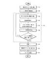
図1は、触媒促進型の原子層堆積法(ALD)によって基板上に二酸化シリコン薄膜を形成する本発明の方法に一般的に適用される複数の段階、処理、連続的な化学反応を概略するフロー図である。FIG. 1 outlines the multiple steps, processes, and sequential chemistry commonly applied to the method of the present invention for forming a silicon dioxide thin film on a substrate by catalyst enhanced atomic layer deposition (ALD). It is a flowchart.
段階110
適当な機能化された基板を反応チャンバに入れる。
A suitable functionalized substrate is placed in the reaction chamber.
段階120
基板の温度が二酸化シリコンALDプロセスを開始するのに適した温度、典型的には約25℃−150℃に達するまで、基板を予備加熱する。
The substrate is preheated until the temperature of the substrate reaches a temperature suitable for initiating the silicon dioxide ALD process, typically about 25C-150C.
段階130
ALDによって、新しい二酸化シリコン層を基板表面に形成する。所望の厚さの二酸化シリコン薄膜が基板上に形成するまでサイクルを繰り返す。段階130は、以下に説明する小段階132−138から成る。
ALD forms a new silicon dioxide layer on the substrate surface. The cycle is repeated until a silicon dioxide thin film of a desired thickness is formed on the substrate.
段階132
第1の反応物と触媒の混合物を反応チャンバに供給する。触媒は基板上で第1の反応物の反応活性化エネルギーを下げるように作用する。結果として、プロセス温度はほぼ室温まで又は室温よりわずかに高い温度まで低下する。
第1の反応物を供給すると、チャンバ内のプロセス温度は典型的には約25℃−150℃であり、好適には約90℃−110℃である。チャンバ内のプロセス圧力は典型的には約0.1〜100torrであり、好適には0.5〜5torrである。不活性ガス、例えば、アルゴン(Ar)を第1の反応物と触媒と共にチャンバに供給してもよい。
−OH反応サイトのHは、ハロゲン酸を形成するために、第1の塩基触媒の存在下で第1の反応物のハロゲン原子と反応する。ハロゲン酸は第1の塩基触媒を用いて中性化され、塩が生成される。同時に、第1の反応物のSi原子は、第1の生成物の化学吸着層を形成するために基板上の反応サイト上で酸素と反応する。
A mixture of a first reactant and a catalyst is supplied to a reaction chamber. The catalyst acts to reduce the reaction activation energy of the first reactant on the substrate. As a result, the process temperature drops to about room temperature or slightly above room temperature.
When the first reactant is provided, the process temperature in the chamber is typically about 25C-150C, preferably about 90C-110C. The process pressure in the chamber is typically between about 0.1 and 100 torr, preferably between 0.5 and 5 torr. An inert gas, such as argon (Ar), may be supplied to the chamber along with the first reactant and the catalyst.
H at the -OH reaction site reacts with a halogen atom of the first reactant in the presence of a first base catalyst to form a halogen acid. The halogen acid is neutralized using a first base catalyst to form a salt. At the same time, the Si atoms of the first reactant react with oxygen on the reaction sites on the substrate to form a first product chemisorption layer.
段落134
第1の反応プロセス(段落132)の副産物、例えば、塩、反応しなかった第1の反応物等を除去する。
By-products of the first reaction process (paragraph 132), such as salts, unreacted first reactants, etc., are removed.
段落136
(O及びHを含む)第2の反応物と第2の塩触媒の混合物をチャンバに供給し、第1の反応物の化学吸着層を第2の反応物と化学的に反応させる。
第2の反応物の例は、H2O、H2O2又はオゾンである。一の実施形態では、第2の塩触媒は第1の塩触媒と同じである。
第2の反応物を反応チャンバに供給するとき、チャンバ内の温度及び圧力の範囲は典型的には、段階132で使用された温度及び圧力の範囲とほぼ同じである。
この段階では、第2の反応物のO元素は、基板表面上に化学吸着したSiと反応する。第2の塩触媒の存在下で、第2の反応物のH元素はハロゲン原子と反応し、それによって、ハロゲン酸を生成する。次いで、このようなハロゲン酸と塩触媒との間の中和によって塩が生成する。
A mixture of a second reactant (including O and H) and a second salt catalyst is provided to the chamber to chemically react the chemisorbed layer of the first reactant with the second reactant.
Examples of the second reactant are H2 O, H2 O2 or ozone. In one embodiment, the second salt catalyst is the same as the first salt catalyst.
When supplying the second reactant to the reaction chamber, the temperature and pressure ranges within the chamber are typically about the same as the temperature and pressure ranges used in
At this stage, the O element of the second reactant reacts with Si chemically adsorbed on the substrate surface. In the presence of a second salt catalyst, the H element of the second reactant reacts with a halogen atom, thereby producing a halogen acid. The salt is then formed by neutralization between such a halogen acid and a salt catalyst.
段落138
第2の反応段階(段階136)の副産物を除去する。
The by-products of the second reaction step (step 136) are removed.
段落140
反応チャンバを排気して、チャンバ内に残留する堆積副産物を除去する。望ましくは、約90秒で段階を完了する。段階140の間、チャンバには気体は供給しない。
The reaction chamber is evacuated to remove deposition byproducts remaining in the chamber. Preferably, the steps are completed in about 90 seconds. During
段落150
その表面に沿ったSiO2薄膜の基板をチャンバから取り出す。
The substrate of the SiO2 thin film along the surface is taken out of the chamber.
段落160
この段階は、新規に堆積したSiO2薄膜を硬化することを含む。本発明によって堆積した二酸化シリコン層を硬化するのに用いられる3つの方法がある。
1.熱処理:実質的な不活性ガス(すなわち、基板表面に対して不活性)例えば、窒素(N2)、酸素(O2)、水素(H2)、アルゴン(Ar)等の存在下で、約300℃−900℃で基板をアニールする。
2.プラズマ処理:酸素(O2)又は水素(H2)の存在下で、約200℃−700℃で基板をアニールする。
3.典型的には約25℃−700℃で、オゾン(O3)処理
This step includes curing the SiO2 thin film deposited on the new. There are three methods used to cure the silicon dioxide layer deposited according to the present invention.
1. Heat treatment: substantially in the presence of an inert gas (ie, inert to the substrate surface), such as nitrogen (N2 ), oxygen (O2 ), hydrogen (H2 ), argon (Ar), etc. Anneal the substrate at 300-900C.
2. Plasma treatment: Anneal the substrate at about 200 ° C.-700 ° C. in the presence of oxygen (O2 ) or hydrogen (H2 ).
3. Ozone (O3) treatment, typically at about 25-700C
先述の3つの硬化法のいずれかを、本発明による触媒補助型ALDプロセスを用いて成長されたSiO2薄膜を使ってインサイチューで用いる。上の硬化方法2及び3が特に良好に働くことがわかった。Any of the three curing methods described above are used in situ with SiO2 thin films grown using the catalyst assisted ALD process according to the present invention. The
第1の実施形態
本発明の第1の実施形態では、第1の反応物としてSi2Cl6又はそれと類似する化合物例えば、2個又は3個以上のシリコン原子を有するシリコンハライド(ハロゲン化物)を;第2の反応物として酸素と水素とを含む化合物例えば、H2O及び/又はH2O2を;触媒として塩化合物例えば、アンモニア又はアミンを;用いて水酸基を有する基板の機能化表面上に二酸化シリコン薄膜を生成する。本発明のこの実施形態では、第1の反応物は少なくとも2個のシリコン原子を有するシリコン化合物、例えば、Si2X6、Si3X8、Si4X10、及び以下の構造を有するSi3X6(三角形)から成る群から選択されたシリコンハライド化合物である。
図2で図示したように、第1の段階において、第1の反応物及び触媒の混合物を基板の水酸基機能化表面に曝すことによって、第1の反応物の化学吸着層を基板表面に沿って形成する。次いで、反応していない第1の反応物及び副産物を基板の領域から除去する。次のプロセス段階では、図2で図示したように、第1の反応物の化学吸着層は、触媒として塩化合物の存在下で第2の化合物と反応する。ここでその触媒は第1の反応物を反応する際に使用されるのと同じ触媒又は異なる塩化合物触媒であってもよい。この第2の反応段階の反応していない第2の反応物と副産物とを基板領域から除去する。新しくSiO2単層を含むようになった基板の表面は、新しいALDサイクルを始めるように準備された水酸基機能化状態に戻る。As illustrated in FIG. 2, in a first step, a mixture of the first reactant and the catalyst is exposed to a hydroxyl functionalized surface of the substrate, thereby causing a chemisorbed layer of the first reactant along the substrate surface. Form. Then, unreacted first reactants and by-products are removed from the region of the substrate. In the next process step, as illustrated in FIG. 2, the chemisorbed layer of the first reactant reacts with the second compound in the presence of a salt compound as a catalyst. Here, the catalyst may be the same catalyst used in reacting the first reactant or a different salt compound catalyst. The unreacted second reactants and by-products of this second reaction stage are removed from the substrate area. Surface of the substrate adapted to new including SiO2 single layer returns to the prepared hydroxyl functional state to begin a new ALD cycle.
前のプロセスはクラウス’442に記載された触媒補助型ALD技術によく似ているが、異なる反応物及び触媒の選択は、基板の薄膜表面層の性質及び品質において急激でかつ劇的なインパクトを呈することがわかった。一の重要な相異は、クラウス’442はSiCl4、すなわち、1個のシリコン原子を有するシリコンハライドの使用を教示する一方、本発明の上述の実施形態は、少なくとも2個のシリコン原子を有するシリコンハライド例えば、Si2Cl6を利用することである。この相異が成長率において大きな改善をもたらすことが本発明でわかった。特に、SiCl4単層は分子間に大きなスペースを有することがわかった。SiCl4の場合には、Si原子は基板上でO−Hサイトと反応し、Oと単結合を形成するときに、SiCl4は回転する。(反応に参加しない)Clの立体障害のために、次のO−Hサイトは他のSiCl4とは反応できない。他方、Si2Cl6単層は同時に2個のSi原子と反応でき、それによって、ALDプロセスの速度を向上する。さらに、その結果、表面に沿ってパッキングする分子がより密になり、二酸化シリコン層の品質が向上する。The previous process is very similar to the catalyst assisted ALD technique described in Claus' 442, but the choice of different reactants and catalysts has a sharp and dramatic impact on the nature and quality of the thin film surface layer of the substrate. It was found to present. One important difference is that Claus' 442 teaches the use of SiCl4 , a silicon halide having one silicon atom, while the above-described embodiments of the present invention have at least two silicon atoms. The use of silicon halide, for example, Si2 Cl6 . It has been found in the present invention that this difference results in a significant improvement in growth rate. In particular, it has been found that a SiCl4 monolayer has a large space between molecules. In the case of SiCl4 , the Si atoms react with O—H sites on the substrate to form a single bond with O, and the SiCl4 rotates. For (non participating in the reaction) Cl sterically hindered, following O-H sites can not react with other SiCl4. On the other hand, a Si2 Cl6 monolayer can react with two Si atoms simultaneously, thereby increasing the speed of the ALD process. In addition, the result is a denser packing of molecules along the surface, improving the quality of the silicon dioxide layer.
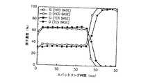
以下に説明するように、図3−図6では、本発明のヘキサクロロシリコン(HCD)を用いて基板に成長したSiO2単層の特性及びパフォーマンスと、クラウス’442のテトラクロロシリコン(TCS)法を用いて成長したSiO2単層とを比較している。As will be described below, FIGS. 3-6 illustrate the properties and performance of the SiO2 single layer grown on the substrate using the hexachlorosilicon (HCD) of the present invention, and the Claus'442 tetrachlorosilicon (TCS) method. Is compared with a SiO2 single layer grown by using the above method.
例えば、図3のグラフでは、種々のプロセス温度において、従来のSiCl4アプローチを用いた基板上へのSiO2単層の堆積速度と、本発明のSi2Cl6技術を利用して得られた堆積速度とを比較している。図3は、全てのプロセス温度で、Si2Cl6を用いた堆積速度(丸印)はSiCl4を用いた堆積速度(正方形印)のほぼ2倍である。For example, in the graph of FIG. 3, at various process temperatures, the deposition rate of a monolayer of SiO2 on a substrate using a conventional SiCl4 approach and obtained using the Si2 Cl6 technology of the present invention. Comparison with the deposition rate. FIG. 3 shows that at all process temperatures, the deposition rate using Si2 Cl6 (circles) is almost twice as high as the deposition rate using SiCl4 (squares).
図4は、従来のTCS(SiCl4)を用いて基板上に成長させた薄膜層の“シリコンリッチさ”と、本発明のHCD(Si2Cl6)を用いて基板上に成長させた薄膜の“シリコンリッチさ”とを比較している。種々のスパッタリング時間で、基板表面上のSiとOの原子濃度を測定するためにオージェ電子分光法を用いて、図4は、TCS技術を用いたOに対するSiの比は1:1.95であり、他方、HCD技術を用いたOに対するSiの比は1:1.84である。言い替えると、HCDアプローチを用いて形成した薄膜SiO2層はシリコンが“よりリッチ”であるのが望ましい。FIG. 4 shows the “silicon richness” of the thin film layer grown on the substrate using the conventional TCS (SiCl4 ) and the thin film grown on the substrate using the HCD (Si2 Cl6 ) of the present invention. Of "silicon richness". Using Auger electron spectroscopy to measure the atomic concentrations of Si and O on the substrate surface at various sputtering times, FIG. 4 shows that the ratio of Si to O using the TCS technique was 1: 1.95. Yes, while the ratio of Si to O using HCD technology is 1: 1.84. In other words, it is desirable for the thin SiO2 layer formed using the HCD approach to be “richer” in silicon.
図5Aは、HCD本発明のアプローチを用いて成長させたSiO2単層においてシリコンのシリコン結合状態と、従来のTCS法を用いて成長させた単層において結合状態とを比較するXPSデータを示す。図5Aのグラフに示された結合状態の差は、図4によって示されたシリコン“リッチさ”の差と共に、SiO2単層はTCS法の代わりにHCD法によって成長されたときに形成された異なるタイプのシリコン結合によって説明されていると思われる。図5Bに図示されているように、TCS法では、SiO2単層における隣接シリコン原子は中間の酸素原子だけを介して相互に結合すると考えられ、他方、本発明のHCD法では、SiO2単層において少なくとも複数の直接のSi−Si結合の生成につながると考えられる。FIG. 5A shows XPS data comparing the silicon bonding state of silicon in a SiO2 monolayer grown using the HCD inventive approach with that in a monolayer grown using a conventional TCS method. . The difference in bonding state shown in the graph of FIG. 5A, together with the difference in silicon “richness” shown in FIG. 4, was formed when the SiO2 monolayer was grown by HCD instead of TCS. It appears to be explained by different types of silicon bonds. As shown in Figure 5B, the TCS method, considered adjacent silicon atoms in the SiO2 single layer is bonded to each other only via the intermediate oxygen atom, and the other, with HCD method of the present invention, SiO2 single It is believed that this leads to the formation of at least a plurality of direct Si-Si bonds in the layer.
図6は、本発明のHCD法を用いて形成されたSiO2薄膜に対するウェットエッチング速度と、従来のTCS法を用いて形成されたSiO2薄膜に対するウェットエッチング速度とを比較する(図6の棒グラフの縦スケールは両データを載せるために不連続になっている)。図6は、本発明のHCD法を用いて形成されたSiO2薄膜のウェットエッチング速度がTCS法を用いて形成されたSiO2薄膜より約6倍良好であることを示している。FIG. 6 compares the wet etching rate for a SiO2 thin film formed using the HCD method of the present invention with the wet etching rate for a SiO2 thin film formed using the conventional TCS method (the bar graph in FIG. 6). The vertical scale of is discontinuous to carry both data). FIG. 6 shows that the wet etching rate of the SiO2 thin film formed by using the HCD method of the present invention is about 6 times better than that of the SiO2 thin film formed by using the TCS method.
第2の実施形態
本発明の第2の実施形態では、第1の反応物としてシリコンハライドと;酸素及び水素原子を含む第2の反応物例えば、H2O及び/又はH2O2と;三元脂肪化合物アミン触媒と;用いて基板の機能化表面上に二酸化シリコン薄膜を生成する。本発明のこの実施形態では、第1のプロセス段階において基板の機能化表面を第1の反応物と触媒との混合物に曝すことによって、第1の反応物の化学吸着層を基板表面に沿って形成する。次いで、反応しなかった第1の反応物と副産物とを基板のその領域から除去する。次のプロセス段階において、第1の反応物の化学吸着層が三元脂肪化合物アミン触媒の存在下で第2の反応物と反応する。この第2のプロセス段階の副産物を基板領域から除去する。Second Embodiment In a second embodiment of the present invention, silicon halide as a first reactant; a second reactant containing oxygen and hydrogen atoms, for example, H2 O and / or H2 O2 ; A tertiary fatty compound amine catalyst to produce a silicon dioxide thin film on the functionalized surface of the substrate. In this embodiment of the invention, the first process step exposes the functionalized surface of the substrate to a mixture of the first reactant and the catalyst to cause a chemisorbed layer of the first reactant along the substrate surface. Form. The unreacted first reactant and by-products are then removed from that region of the substrate. In the next process step, the first reactant chemisorption layer reacts with the second reactant in the presence of the ternary fatty compound amine catalyst. By-products of this second process step are removed from the substrate area.
本発明の実施形態について、反応触媒として第三脂肪族アミンの使用によって、プロセス効率、望まない副産物の除去又は最小化によって、及び、基板に堆積されたSiO2薄膜の純度及び品質において、新規でかつ全く不測の効果を奏する。さらに詳細には、一の窒素−水素(N−H)結合を有するアミン、例えば、アンモニア(NH3)、一元又は二元の脂肪族アミン(NR、H2、又はNR2H)を触媒として用いるならば、以下の式(1)及び(2)に示したように、シリコン−窒素(Si−N)結合を有する望まない副産物を形成する傾向があることがわかった:
(1)SiCl4+NR2H → Cl3Si−NR2+HCl
(2)SiCl4+NH3 → Cl3Si−NH4+Cl−(塩)
ここで、Rは1個から5個程度の炭素原子を有する脂肪族群(CxHy)であり、脂肪族群Rは同じでも異なっていてもよい。Embodiments of the present invention, by the use of a tertiary aliphatic amine as a reaction catalyst, process efficiency, the removal or minimization of by-products is not desired, and, in the purity and quality of the SiO2 thin films deposited on the substrate, a new And it has a completely unexpected effect. More particularly, one nitrogen - amine having a hydrogen (NH) bond, for example, ammonia(NH 3), one yuan or two-source aliphatic amines (NR,H 2, orNR 2 H) as a catalyst If used, it has been found that there is a tendency to form unwanted by-products with silicon-nitrogen (Si-N) bonds, as shown in equations (1) and (2) below:
(1) SiCl4 + NR2 H → Cl3 Si—NR2 + HCl
(2) SiCl4 + NH3 → Cl3 Si—NH4+ Cl− (salt)
Wherein, R is an aliphatic group having one to about five carbon atoms (C xHy), aliphatic group R may be the same or different.
しかしながら、(例えば、上述の式(1)及び(2)の右側に示したように)、表面層不純物につながる粒子の形成の主要な原因であり、堆積されたSiO2薄膜の品質を劣化することがわかった。対照的に、一般式NR3を有する第三脂肪族アミン(ここで、Rは1個から5個程度の炭素原子を有する脂肪族群(CxHy))が反応触媒として使用されるならば、シリコン−窒素(Si−N)結合を有する特別の副産物を実質的に形成しないことがわかっている。結果として、本発明の方法によって、より高品質でかつ優れた均一性を有するはるかに高純度のSiO2薄膜が堆積される。However, (for example, as shown on the right side of the above equation (1) and (2)), the leading cause of formation of particles leading to the surface layer impurities, degrades the quality of the SiO2 thin films deposited I understand. In contrast, the general formula NR3 tertiary aliphatic amine (wherein, R represents an aliphatic group (C xH y) having one 5 or so carbonatoms) with if it is used as a reaction catalyst, It has been found that substantially no special by-products having silicon-nitrogen (Si-N) bonds are formed. As a result, much higher purity SiO2 thin films with higher quality and better uniformity are deposited by the method of the present invention.
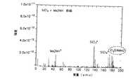
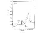
以下で議論する図7及び表3は、この知見の有効性と顕著な重要性を証明している。図7は、第三脂肪族アミンでないアミン触媒を用いてALDプロセスを実施するとき、固体の特別な副産物の形成を確認するRGA分析の結果である。図7は、第1の反応物としてSiCl4と、触媒してジメチルアミン((H3C)2NH)、すなわちN−H単結合を有するアミンとを用いるクラウス’442において教示された触媒型ALDプロセスに基づいている。残留質量スペクトル装置を、反応物からの副産物を分析するためにALD反応チャンバに結合した。図7の質量スペクトルでは、反応物の望まない(不必要な)副産物としてCl3Si−N(CH3)2の形成を確認した。このような副産物の形成は、SiCl4第1の反応物からSiのいくつかが、SiO2として基板表面に堆積する代わりに、副産物を形成する際に浪費されたことを意味する。FIG. 7 and Table 3, discussed below, demonstrate the validity and significant importance of this finding. FIG. 7 is the result of an RGA analysis confirming the formation of a solid by-product when performing the ALD process using an amine catalyst that is not a tertiary aliphatic amine. FIG. 7 shows the catalyst type taught in Claus' 442 using SiCl4 as the first reactant and dimethylamine ((H3 C)2 NH), an amine having an NH single bond, as the catalyst. Based on the ALD process. A residual mass spectrometer was coupled to the ALD reaction chamber for analyzing by-products from the reaction. The mass spectrum of FIG. 7 confirmed the formation of Cl3 Si—N (CH3 )2 as an unwanted (unwanted) by-product of the reactants. The formation of such by-products means that some of the Si from the SiCl4 first reactant was wasted in forming by-products instead of depositing on the substrate surface as SiO2 .
従来技術に対する本発明の実施形態の利点の他の証拠を以下の表3に示した。
表3では、第1の反応物としてSiCl4を用い、触媒として異なるアミンを用いて触媒型ALDが実施されたときに同じ領域の基板表面に堆積された(少なくとも0.16μmのサイズを有する)望まない粒子の数を比較している。表3は、ALD触媒としてSiCl4すなわち3個のN−H結合を有する分子を用いて、ALDプロセスがSiO2薄膜の表面上に数万の副産物粒子を生ずる。SiO2薄膜上のこの非常に高いレベルの粒子のコンタミネーションは半導体装置のパフォーマンスに反対に影響を与え、非常に過酷な現代の半導体用途の多くに対して全く受け入れられないものである。In Table 3, the desired (having a size of at least 0.16 μm) deposited on the same area of the substrate surface when catalytic ALD was performed using SiCl4 as the first reactant and a different amine as the catalyst. Not comparing the number of particles. Table 3 shows that, using SiCl4 , a molecule with three NH bonds, as the ALD catalyst, the ALD process produces tens of thousands of by-product particles on the surface of the SiO2 thin film. Contamination of the very high level of particles on the SiO2 thin film affects the opposition to the performance of the semiconductor device, in which totally unacceptable for many highly demanding modern semiconductor applications.
表3は、ALD触媒としてジメチルアミン、すなわち単一の攻撃されやすいN−H結合の使用は、約1桁のオーダーで粒子状副産物を低減するのに有効であることを示している。ジメチルアミン触媒と共に得られるように、SiO2薄膜上に数1000の範囲で粒子製造でさえ、非常に高いパフォーマンスの半導体装置に対する許容範囲を越えている。表3は、ALD触媒としてトリメチルアミンを使用して、それによって攻撃されやすい全N−H結合を除去することによって、アンモニアに対して3桁のオーダーの減少であり、ジメチルアミンに対して2桁のオーダーである数10まで副産物粒子の生成を減少するという劇的でかつ不測の結果を示していることを明らかにしている。、Table 3 shows that the use of dimethylamine, a single vulnerable NH bond, as an ALD catalyst is effective in reducing particulate by-products on the order of about an order of magnitude. Even in the range of thousands of particles on SiO2 thin films, as obtained with a dimethylamine catalyst, is beyond the acceptable range for very high performance semiconductor devices. Table 3 shows that using trimethylamine as an ALD catalyst, thereby removing all vulnerable NH bonds, results in a three orders of magnitude reduction for ammonia and two orders of magnitude for dimethylamine. It reveals a dramatic and unexpected result of reducing the formation of by-product particles to the order of tens. ,
従来技術に対する本発明のこの実施形態の他の利点は、この本発明の実施形態が、例えば、クラウス’442特許において好適な触媒であるピリジンの代わりに第三脂肪族アミン触媒を使用することである。ピリジンは、C5H5Nの化学式を有して5個の炭素原子及び1個の窒素原子のリングを含む異種環状化合物である。これは室温で、刺激的で特徴的な臭いを有しかつ十分に取り扱いに注意を要する有毒液体として存在する。ALDプロセスにおいて触媒として用いられるときは、ピリジンは蒸発して気体状態(ピリジンの沸点は115.5℃)になる。従って、ピリジンを処理する装備は複雑であり、ピリジン供給ラインは容易に汚染される。Another advantage of this embodiment of the present invention over the prior art is that this embodiment of the present invention uses a tertiary aliphatic amine catalyst instead of pyridine, which is a preferred catalyst in, for example, the Claus' 442 patent. is there. Pyridine is heterologous cyclic compound containing a
対照的に、低分子量の第三脂肪族アミン例えば、トリメチルアミンは周囲条件で気体であり、それによって通常の反応条件で相変化を生じる傾向がある触媒より使用を容易になっている。さらに、トリメチルアミンの毒性はピリジンの毒性よりはるかに低く、トリメチルアミンの沸点は3〜4℃である。In contrast, low molecular weight tertiary aliphatic amines, such as trimethylamine, are gaseous at ambient conditions, thereby making them easier to use than catalysts that tend to undergo a phase change under normal reaction conditions. Furthermore, the toxicity of trimethylamine is much lower than that of pyridine, and the boiling point of trimethylamine is 3-4 ° C.
第3の実施形態
本発明の第3の好適な実施形態では、本発明の先述の2つの実施形態の利点と効果の全ては実現できない場合は多い。この実施形態では、第1の反応物として少なくとも2個又は3個以上のシリコン原子を有するシリコン化合物すなわちSi2Cl6のようなシリコンハライドと、第2の反応物としてO原子及びH原子を含む化合物例えば、H2O及び/又はH2O2と、第三脂肪族アミン触媒とを用いて、基板の機能化表面上に二酸化シリコン薄膜を成長させる。 Third Embodiment In the third preferred embodiment of the present invention, it is often not possible to realize all of the advantages and effects of the above two embodiments of the present invention. In this embodiment, the first reactant includes a silicon compound having at least two or more silicon atoms, ie, a silicon halide such as Si2 Cl6 , and the second reactant includes O atoms and H atoms. A silicon dioxide thin film is grown on a functionalized surface of a substrate using a compound, for example, H2 O and / or H2 O2 and a tertiary aliphatic amine catalyst.
この本発明の実施形態では、基板表面に沿って第1の反応物の化学吸着層を形成するために、第1のプロセス段階において、第1の反応物と第三脂肪族アミン触媒の混合物に、基板の機能化表面を曝す。反応しなかった第1の反応物と副産物とを基板の領域から除去する。次のプロセス段階では、第1の反応物の化学吸着層は、第三脂肪族アミン触媒の存在下で第2の反応物と反応する。この第2の反応段階の副産物を基板領域から除去する。In this embodiment of the present invention, a mixture of the first reactant and the tertiary aliphatic amine catalyst is applied in a first process step to form a first reactant chemisorption layer along the substrate surface. Expose the functionalized surface of the substrate. Unreacted first reactants and by-products are removed from regions of the substrate. In the next process step, the first reactant chemisorption layer reacts with the second reactant in the presence of a tertiary aliphatic amine catalyst. By-products of this second reaction stage are removed from the substrate area.
本発明の他の実施形態では、図1の複数のプロセス段階132−138のうちの一又は二以上に対して気体パルス/パージ法の使用によって、本発明の方法の効率を改善し、プロセスコンタミネーションを除去し、基板上に形成されたSiO2薄膜の質を改善することができることがわかった。図8は、以下に記載するように、図1の段階132−138を実施する気体パルス法を図示するものである。In another embodiment of the present invention, the use of a gas pulse / purge method for one or more of the plurality of process steps 132-138 of FIG. It has been found that the cation can be removed and the quality of the SiO2 thin film formed on the substrate can be improved. FIG. 8 illustrates a gas pulse method for performing steps 132-138 of FIG. 1, as described below.
段階132
第1の反応物と適当な触媒とを独立の各供給ラインを介して反応チャンバに流す。このとき、第1の反応物と触媒の混合ガスからのコンタミネーションを回避するために、第2の反応供給ラインを介して不活性ガス例えば、アルゴンガスをチャンバに流すことができる。
The first reactant and the appropriate catalyst are flowed into the reaction chamber via independent supply lines. At this time, an inert gas, for example, an argon gas can be flowed into the chamber via the second reaction supply line in order to avoid contamination from the mixed gas of the first reactant and the catalyst.
段階134
パージのための不活性ガスを、第1の反応物供給ラインと第2の反応物供給ラインと触媒供給ラインとを介してチャンバに流し込む。
Inert gas for purging flows into the chamber via the first reactant supply line, the second reactant supply line, and the catalyst supply line.
段階136
O原子とH原子とを含む第2の反応物と適当な触媒とを、独立の各供給ラインを介してチャンバに流し込む。このとき、第1の反応物供給ラインをパージするため、第1の反応物供給ラインを介して、不活性ガス例えば、アルゴンガスをチャンバ内に流し込むことができる。
A second reactant containing O and H atoms and a suitable catalyst are flowed into the chamber via each independent supply line. At this time, in order to purge the first reactant supply line, an inert gas, for example, argon gas can be flowed into the chamber through the first reactant supply line.
段階138
パージのための不活性ガスを、第1の反応物供給ラインと第2の反応物供給ラインと触媒供給ラインとを介してチャンバに流し込む。
Inert gas for purging flows into the chamber via the first reactant supply line, the second reactant supply line, and the catalyst supply line.
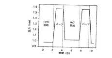
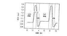
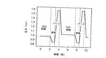
10秒間のプロセス時間間隔(インターバル)にわたって、図1の段階132−138に対応して、種々のフィードラインと反応物チャンバに気体のパルス送り/排気又はパージについての複数の代表的な“レシピ”又はシーケンスを、図9−図12に示す。図9は、副産物をパージし除去するために不活性ガスを用いて選択したプロセス時間間隔で行われる1サイクルに以下の段階を備えたプロセスパージシーケンスを示している:0−2秒プロセス時間−HCD供給;2−4秒プロセス時間−パージ;4−7.5秒プロセス時間−H2O供給;7.5−10秒プロセス時間−パージ。図10は、1サイクルにおいて連続する以下の段階を備えた、排気圧力が第1及び第2の反応物供給圧力より低いプロセス排気シーケンスを示す:0−2秒プロセス時間−HCD供給;2−4秒プロセス時間−排気;4−7.5秒プロセス時間−H2O供給;7.5−10秒プロセス時間−排気。図11は、1サイクルにおいて連続する以下の段階を備えた、排気がパージ後に用いられるプロセスパージ−排気シーケンスを示す:0−2秒プロセス時間−HCD供給;2−3秒プロセス時間−パージ;3−4秒プロセス時間−排気;4−7.5秒プロセス時間−H2O供給;7.5−8.5秒プロセス時間−パージ:8.5−10秒プロセス時間−排気。図12は、1サイクルにおいて連続する以下の段階を備えた、パージが排気後に用いられるプロセス排気−パージシーケンスを示す:0−2秒プロセス時間−HCD供給;2−3秒プロセス時間−排気;3−4秒プロセス時間−パージ;4−7.5秒プロセス時間−排気;7.5−8.5秒プロセス時間−排気:8.5−10秒プロセス時間−パージ。 Several representative "recipe" for pulsing / evacuating or purging gas to various feed lines and reactant chambers over a 10 second process time interval, corresponding to steps 132-138 of FIG. Alternatively, the sequence is shown in FIGS. FIG. 9 shows a process purge sequence in which one cycle performed at selected process time intervals using an inert gas to purge and remove by-products comprises the following steps: 0-2 seconds process time— HCD supply; 2-4 seconds process time - purge; 4-7.5 seconds process time -H2 O supply; 7.5-10 seconds process time - purge. FIG. 10 shows a process exhaust sequence in which the exhaust pressure is lower than the first and second reactant feed pressures, with the following steps in one cycle: 0-2 seconds process time-HCD feed; 2-4 seconds process time - exhaust; 4-7.5 seconds process time -H2 O supply; 7.5-10 seconds process time - the exhaust. FIG. 11 shows a process purge-evacuation sequence in which the exhaust is used after purging with the following steps in one cycle: 0-2 seconds process time-HCD supply; 2-3 seconds process time-purge; 3 -4 sec process time - exhaust; 4-7.5 seconds process time -H2 O supply; 7.5-8.5 seconds process time - purge: 8.5-10 seconds process time - the exhaust. FIG. 12 shows a process evacuation-purge sequence in which a purge is used after evacuation with the following steps in one cycle: 0-2 seconds process time-HCD supply; 2-3 seconds process time-exhaust; 3 -4 seconds process time-purge; 4-7.5 seconds process time-exhaust; 7.5-8.5 seconds process time-exhaust: 8.5-10 seconds process time-purge.
本発明の他の実施形態では、本発明によって基板上にSiO2薄膜を成長させるために触媒補助型ALDを実施する温度条件は、2つの競合するプロセスパラメータを調和させることによって最適化する。図13に図示したように、一方で、触媒補助型ALDと第1の反応物として複数のシリコン原子を有する化合物(例えば、Si2Cl6)を用いてSiO2を形成する際の堆積速度は、温度に反比例する。図13は、一般に、プロセス温度が高いほど、堆積速度が低いことを示している。これは堆積速度に起因すると思われ、ALDが表面反応なので、それはALDプロセスの特有の特徴である。プロセス温度が高いほど、反応に参加する原子の表面脱離活性エネルギーは高い。結果として、表面での“滞在時間”は、以下の式に従って、反応が生ずるのに要する最小時間より短縮される:
A:アレニウス定数
Ed:脱離活性エネルギー
R:気体定数
T:温度 In another embodiment of the present invention, temperature conditions for implementing the catalyst-assisted ALD to grow the SiO2 thin film on a substrate by the present invention is optimized by harmonizing the process parameters of two competing. As illustrated in FIG. 13, on the other hand, the deposition rate when forming SiO2 using a catalyst-assisted ALD and a compound having a plurality of silicon atoms (eg, Si2 Cl6 ) as a first reactant is: , Which is inversely proportional to temperature. FIG. 13 shows that, generally, the higher the process temperature, the lower the deposition rate. This may be due to the deposition rate, and because ALD is a surface reaction, it is a unique feature of the ALD process. The higher the process temperature, the higher the surface desorption activation energy of the atoms participating in the reaction. As a result, the "stay time" at the surface is reduced from the minimum time required for the reaction to take place according to the following equation:
プロセス温度が高いほど、基板表面でのO−H鎖の脱ヒドロキシル化(脱水酸化)が容易になる。従って、表面に沿った反応サイトの数は減少し、堆積速度は小さくなる。The higher the process temperature, the easier the dehydroxylation (dehydroxylation) of the O—H chains on the substrate surface. Thus, the number of reaction sites along the surface is reduced and the deposition rate is reduced.
他方、図14に図示したように、3個の異なるプロセス温度での炭素含有量の経時変化のSIMS(二次イオンマススペクトロメータ)グラフでは、ALD堆積SiO2薄膜の炭素含有量もプロセス温度によって変化する。通常、低温プロセス温度では、ALD反応過程の炭素含有副産物は、プロセス中に基板表面から十分には除去されなく、堆積するSiO2薄膜に捕捉される。それによる薄膜の不純物レベルの増大によって、半導体装置の質は低下する。On the other hand, as shown in FIG. 14, the SIMS (secondary ion mass spectrometer) graph of the carbon content with time at three different process temperatures shows that the carbon content of the ALD deposited SiO2 thin film also depends on the process temperature. Change. Usually, in the low temperature process temperature, carbon-containing by-product of the ALD reaction process, it is sufficiently from the substrate surface during the process no longer removed, is captured in the SiO2 thin film deposited. As a result, the quality of the semiconductor device deteriorates due to the increase in the impurity level of the thin film.
従って、これらの2つのプロセスパラメータは、プロセス温度条件を最適化するために互いに釣り合わなければならない。先述の考察に基づいて、本発明のこの実施形態において、最適プロセス温度範囲は約90℃−110℃であることがわかった。Therefore, these two process parameters must balance each other to optimize the process temperature conditions. Based on the foregoing discussion, it has been found that in this embodiment of the invention, the optimal process temperature range is about 90-110 ° C.
本発明の他の実施形態では、本発明に従って基板上にSiO2薄膜を成長させるために触媒補助型ALDを実施する圧力条件は、2つの競合するプロセスパラメータを調和させることによって最適化する。図15に図示したように、一方で、触媒補助型ALDを用いてSiO2を形成する際の堆積速度は、圧力に反比例する。すなわち、圧力が高いほど、所定の時間間隔/ALDサイクル数にわたって堆積されたSiO2膜は厚い。In another embodiment of the present invention, the pressure conditions for carrying out the catalytic assisted ALD to grow the SiO2 thin film on a substrate in accordance with the present invention is optimized by harmonizing the process parameters of two competing. As shown in FIG. 15, on the other hand, the deposition rate when forming SiO2 using catalyst-assisted ALD is inversely proportional to pressure. That is, the higher the pressure, the thicker the SiO2 film deposited over a given time interval / ALD cycle number.
他方、図16は、SiO2薄膜のプロセス圧力と非均一度(性)との間に非線形関係が存在することを示している。従って、図16は、ある点まで、より高いプロセス圧力が堆積された層の非均一度を低減する;しかし、この点を越えると、より高い圧力はより高い非均一度と相関する。On the other hand, FIG. 16 shows that a non-linear relationship exists between the process pressure of the SiO2 thin film and the non-uniformity (property). Thus, FIG. 16 shows that up to a certain point, higher process pressure reduces the non-uniformity of the deposited layer; however, beyond this point, higher pressure correlates with higher non-uniformity.
従って、これらのプロセスパラメータは、プロセス圧力条件を最適化するために、互いに釣り合わなければならない。以上の考察をもとに、本発明の実施形態に対応して、最適プロセス圧力範囲が約50mmTorr〜約5Torrの範囲であると決定された。Thus, these process parameters must be balanced with each other to optimize the process pressure conditions. Based on the above considerations, it has been determined that the optimal process pressure range is from about 50 mmTorr to about 5 Torr, corresponding to embodiments of the present invention.
ここに記載された本発明の範囲を逸脱することなく、高パフォーマンス半導体装置における使用のために、基板表面上でのSiO2薄膜の上述の改良型触媒補助ALD形成について、さらに他の変更及び変形が可能であることは当業者には明らかであり、上述の詳細な説明に含まれる全事項は例示に過ぎず、限定的な意味に解釈されてはならないことは理解されたい。Without departing from the scope of the invention described herein, for use in high-performance semiconductor device, the above-mentioned improved catalysts assist ALD formation of the SiO2 thin film on the substrate surface, yet other modifications and variations It is clear to a person skilled in the art that this is possible, and it is to be understood that all matter contained in the above detailed description is merely illustrative and should not be construed in a limiting sense.
Claims (43)
Translated fromJapanese以下の段階(a)から段階(c)、すなわち、;
(a)少なくとも2つのシリコン原子を有するシリコン化合物から成る群から選択された少なくとも一の要素を含む第1の反応物を用いる段階;
(b)第三脂肪族アミン化合物から成る群から選択された少なくとも一の要素を含む第1の触媒を用いる段階;
(c)少なくとも2つのシリコン原子を有するシリコン化合物から成る群から選択された少なくとも一の要素を含む第1の反応物を用いることと、第三脂肪族アミン化合物から成る群から選択された少なくとも一の要素を含む第1の触媒を用いることと、を組み合わせて用いる段階;
のうちの少なくとも一又は二以上を備える方法。A method for forming a silicon dioxide layer on a substrate surface of a semiconductor product using a catalyst assisted atomic layer deposition process, wherein the functionalized surface of the substrate comprises a first mixture comprising a first reactant and a first catalyst. And subsequently exposing the surface to a second mixture of a second reactant and a second catalyst to form a silicon dioxide monolayer on the substrate surface. In the method,
The following steps (a) to (c):
(A) using a first reactant comprising at least one member selected from the group consisting of a silicon compound having at least two silicon atoms;
(B) using a first catalyst comprising at least one element selected from the group consisting of tertiary aliphatic amine compounds;
(C) using a first reactant comprising at least one element selected from the group consisting of silicon compounds having at least two silicon atoms; and using at least one reactant selected from the group consisting of tertiary aliphatic amine compounds. Using a first catalyst comprising the elements of:
A method comprising at least one or more of the foregoing.
(a)N2、O2、H2、及びArから成る群から選択された不活性ガスの存在下で、約300℃−900℃で二酸化シリコン層をアニールすることを備えた熱処理;
(b)O2又はH2の存在下で、約200℃−700℃で二酸化シリコン層をアニールすることを備えたプラズマ処理;
(c)約25℃−700℃で、二酸化シリコン層をO3に曝すことを備えたオゾン処理;
のうちの一つから選択されたものである請求項17に記載の方法。The curing step is as follows:
(A) in the presence ofN 2, O 2, H 2 , and an inert gas selected from the group consisting of Ar, heat treatment with the annealing the silicon dioxide layer at about 300 ° C. -900 ° C.;
(B) plasma treatment comprising annealing the silicon dioxide layer at about 200 ° C.-700 ° C. in the presence of O2 or H2 ;
(C) ozone treatment at about 25 ° C. to 700 ° C., comprising exposing the silicon dioxide layer to O3 ;
18. The method of claim 17, wherein the method is selected from one of the following:
プロセス時間長t1の間、前記基板を含む領域に前記第1の反応物と第1の触媒とを供給する段階:時間長t1の直後に、時間長t2の間、領域を不活性ガスでパージする段階:時間長t2の直後に、時間長t3の間、領域から不活性ガスと他の気体物質を少なくとも部分的に排出するために領域を排気する段階:時間長t3の直後に、時間長t4の間、前記第2の反応物と第2の触媒とを領域へ供給する段階:時間長t4の直後に、時間長t5の間、領域を不活性ガスでパージする段階:時間長5の直後に、時間長t6の間、領域から不活性ガスと他の気体物質とを少なくとも部分的に排出するために領域を排気する段階:というシーケンスに従って各原子層堆積のためにパージ−排気処理を備えた請求項1に記載の方法。The following sequence:
Supplying the first reactant and the first catalyst to the region including the substrate for a process time length t1 : inactivating the region for a time length t2 immediately after the time length t1 step purging with gas: immediately after the time length t2, during the duration t3, step to evacuate the area in order to at least partially discharge the inert gas and other gaseous materials from the region: the time length t3 immediately after, during the time length t4, the second reactant and a second catalyst comprising: a supply to the region of: immediately after the time length t4, during the time length t5, the region inert gas in purging steps: immediately after the time length5, during the duration t6, the step of evacuating the space to at least partially discharge the inert gas and other gaseous materials from the region: the atoms in accordance with the sequence of The method of claim 1, comprising a purge-pump process for layer deposition.
プロセス時間長t1の間、前記基板を含む領域に前記第1の反応物と第1の触媒とを供給する段階:時間長t1の直後に、時間長t2の間、領域から少なくとも部分的に気体物質を排出するために領域を排気する段階:時間長t2の直後に、時間長t3の間、領域を不活性ガスでパージする段階:時間長t3の直後に、時間長t4の間、前記第2の反応物と第2の触媒とを領域へ供給する段階:時間長t4の直後に、時間長t5の間、領域から気体物質を少なくとも部分的に排出するために領域を排気する段階:時間長5の直後に、時間長t6の間、領域を不活性ガスでパージする段階:というシーケンスに従って各原子層堆積のためにパージ−排気処理を備えた請求項1に記載の方法。The following sequence:
Supplying the first reactant and the first catalyst to the region including the substrate during a process time length t1 : immediately after the time length t1 , at least partially from the region for a time length t2. stepwise evacuating the region in order to discharge the gaseous substance: immediately after the length of time t2, during the duration t3, step purging region with inert gas: immediately after the length of time t3, the time length between t4, the second reactant and a second catalyst comprising: a supplied to the region: immediately after the length of time t4, during the time length t5, at least partially discharging the gaseous material from the area step to evacuate the area for: just after a time lengthof 5, during the duration t6, the step of purging the space with an inert gas: purge for each atomic layer deposition in accordance with the sequence of - claims having an exhaust treatment Item 2. The method according to Item 1.
(b)第1の反応物と触媒と任意で不活性ガスとをチャンバに供給する段階であって、前記第1の反応物は少なくとも2個のシリコン原子を有するシリコンハライド化合物であり、前記触媒はアンモニアとアミンから成る群から選択されたものである段階と;
(c)反応副産物と反応しなかった第1の反応物と触媒とをチャンバからパージする段階と;
(d)第2の反応物と触媒と任意で不活性ガスとをチャンバに供給する段階であって、前記第2の反応物は酸素成分を有する化合物であり、前記触媒はアンモニアとアミンとから成る群から選択されたものである段階と;
(e)反応副産物と反応しなかった第2の反応物と触媒とをチャンバからパージする段階と;
(f)二酸化シリコン薄膜が所望の膜厚になるまで段階(a)−(e)を繰り返す段階と;
を備えた基板表面に二酸化シリコン薄膜を形成する方法。(A) introducing a substrate into the chamber;
(B) supplying a first reactant, a catalyst, and optionally an inert gas to a chamber, wherein the first reactant is a silicon halide compound having at least two silicon atoms; Is selected from the group consisting of ammonia and amines;
(C) purging the first reactant and catalyst that have not reacted with the reaction by-product from the chamber;
(D) supplying a second reactant, a catalyst, and optionally an inert gas to the chamber, wherein the second reactant is a compound having an oxygen component, and the catalyst comprises ammonia and an amine; A step selected from the group consisting of:
(E) purging the second reactant and catalyst that have not reacted with the reaction by-product from the chamber;
(F) repeating steps (a)-(e) until the silicon dioxide thin film has a desired thickness;
A method of forming a silicon dioxide thin film on the surface of a substrate provided with.
プロセス時間長t1の間、前記チャンバに前記第1の反応物と触媒とを供給する段階;時間長t1の直後に、時間長t2の間、チャンバを不活性ガスでパージする段階;時間長t2の直後に、時間長t3の間、チャンバから不活性ガスと他の気体物質を少なくとも部分的に排出するために領域を排気する段階;時間長t3の直後に、時間長t4の間、前記第2の反応物と触媒とをチャンバへ供給する段階:時間長t4の直後に、時間長t5の間、チャンバを不活性ガスでパージする段階:時間長5の直後に、時間長t6の間、チャンバから不活性ガスと他の気体物質とを少なくとも部分的に排出するために領域を排気する段階:というシーケンスに従って実施する請求項21に記載の方法。 The steps from step (b) to step (e) are performed in the following sequence:
Supplying the first reactant and catalyst to the chamber for a process time length t1 ; immediately after the time length t1 , purging the chamber with an inert gas for a time length t2 ; immediately after the time length t2, during the duration t3, step to evacuate the area in order to at least partially discharge the inert gas and other gaseous material from the chamber; immediately after the duration t3, the time length between t4, the second reactant and the catalyst comprising: a supplying to the chamber: immediately after the time length t4, during the time length t5, step purging the chamber with an inert gas: the time length5 immediately after, during duration t6, the step of evacuating the space to at least partially discharge the inert gas and other gaseous material from the chamber: the method of claim 21 carried out according to the sequence of.
プロセス時間長t1の間、前記チャンバに前記第1の反応物と触媒とを供給する段階;時間長t1の直後に、時間長t2の間、チャンバから少なくとも部分的に気体物質を排出するためにチャンバを排気する段階;時間長t2の直後に、時間長t3の間、チャンバを不活性ガスでパージする段階;時間長t3の直後に、時間長t4の間、前記第2の反応物と触媒とをチャンバへ供給する段階;時間長t4の直後に、時間長t5の間、チャンバから気体物質を少なくとも部分的に排出するためにチャンバを排気する段階;時間長5の直後に、時間長t6の間、チャンバを不活性ガスでパージする段階:というシーケンスに従って実施する請求項21に記載の方法。The steps from step (b) to step (e) are performed in the following sequence:
During the process duration t1, wherein the step of providing a first reactant and catalyst into the chamber; discharge immediately after the time length t1, during the length of time t2, at least partially gaseous material from the chamber immediately after the time length t2, during the duration t3, step purging the chamber with an inert gas; step of evacuating the chamber to immediately after the duration t3, during the time length t4, the immediately after the time length t4, during the time length t5, step to evacuate the chamber to at least partially discharge the gaseous material from the chamber; a second reactant and a catalyst comprising the steps of supplying to the chamber time immediately after the long5, during the duration t6, the step of purging the chamber with an inert gas: the method of claim 21 carried out according to the sequence of.
(b)第1の反応物と触媒と任意で不活性ガスとをチャンバに供給する段階であって、前記第1の反応物はシリコンハライド化合物であり、前記触媒は第三脂肪族アミンである段階と;
(c)チャンバから反応副産物と反応しなかった第1の反応物と触媒をパージする段階と;
(d)第2の反応物と触媒と任意で不活性ガスとをチャンバに供給する段階であって、前記第2の反応物は酸素成分を有する化合物であり、前記触媒はアンモニアとアミンとから成る群から選択されたものである段階と;
(e)チャンバから反応副産物と反応しなかった第2の反応物と触媒をパージする段階と;
(f)二酸化シリコン薄膜が所望の膜厚になるまで段階(a)−(e)を繰り返す段階と;
を備えた基板表面に二酸化シリコン薄膜の形成する方法。(A) introducing a substrate into the chamber;
(B) supplying a first reactant, a catalyst, and optionally an inert gas to the chamber, wherein the first reactant is a silicon halide compound and the catalyst is a tertiary aliphatic amine; Stages;
(C) purging the first reactant and catalyst that have not reacted with the reaction by-products from the chamber;
(D) supplying a second reactant, a catalyst, and optionally an inert gas to the chamber, wherein the second reactant is a compound having an oxygen component, and the catalyst comprises ammonia and an amine; A step selected from the group consisting of:
(E) purging the second reactant and catalyst that have not reacted with the reaction by-products from the chamber;
(F) repeating steps (a)-(e) until the silicon dioxide thin film has a desired thickness;
A method of forming a silicon dioxide thin film on a substrate surface provided with.
プロセス時間長t1の間、前記チャンバに前記第1の反応物と触媒とを供給する段階;時間長t1の直後に、時間長t2の間、チャンバを不活性ガスでパージする段階;時間長t2の直後に、時間長t3の間、チャンバから不活性ガスと他の気体物質とを少なくとも部分的に排出するために領域を排気する段階;時間長t3の直後に、時間長t4の間、前記第2の反応物と触媒とをチャンバへ供給する段階:時間長t4の直後に、時間長t5の間、チャンバを不活性ガスでパージする段階:時間長5の直後に、時間長t6の間、チャンバから不活性ガスと他の気体物質とを少なくとも部分的に排出するために領域を排気する段階:というシーケンスに従って実施することを備えた請求項30に記載の方法。 The steps from step (b) to step (e) are performed in the following sequence:
Supplying the first reactant and catalyst to the chamber for a process time length t1 ; immediately after the time length t1 , purging the chamber with an inert gas for a time length t2 ; immediately after the time length t2, during the duration t3, step to evacuate the area in order to at least partially discharge the inert gas and other gaseous material from the chamber; immediately after the duration t3, time during the long t4, the second reactant and the catalyst comprising: a supplying to the chamber: immediately after the time length t4, during the time length t5, step purging the chamber with an inert gas: time length5 immediately after, during the length of time t6, the step of evacuating the space to at least partially discharge the inert gas and other gaseous material from the chamber: in claim 30 which includes a be carried out in accordance with the sequence of The described method.
プロセス時間長t1の間、前記チャンバに前記第1の反応物と触媒とを供給する段階;時間長t1の直後に、時間長t2の間、チャンバから少なくとも部分的に気体物質を排出するためにチャンバを排気する段階;時間長t2の直後に、時間長t3の間、チャンバを不活性ガスでパージする段階;時間長t3の直後に、時間長t4の間、前記第2の反応物と触媒とをチャンバへ供給する段階;時間長t4の直後に、時間長t5の間、チャンバから気体物質を少なくとも部分的に排出するためにチャンバを排気する段階;時間長5の直後に、時間長t6の間、チャンバを不活性ガスでパージする段階:というシーケンスに従って実施することを備えた請求項30に記載の方法。The steps from step (b) to step (e) are performed in the following sequence:
During the process duration t1, wherein the step of providing a first reactant and catalyst into the chamber; discharge immediately after the time length t1, during the length of time t2, at least partially gaseous material from the chamber immediately after the time length t2, during the duration t3, step purging the chamber with an inert gas; step of evacuating the chamber to immediately after the duration t3, during the time length t4, the immediately after the time length t4, during the time length t5, step to evacuate the chamber to at least partially discharge the gaseous material from the chamber; a second reactant and a catalyst comprising the steps of supplying to the chamber time immediately after the long5, during the duration t6, the step of purging the chamber with an inert gas: the method of claim 30 comprising a be carried out according to the sequence of.
(a)基板をチャンバに導入する段階と;
(b)第1の反応物と触媒と任意で不活性ガスとをチャンバに供給する段階であって、前記第1の反応物は少なくとも2個のシリコン原子を有するシリコンハライド化合物であり、前記触媒はアンモニアとアミンから成る群から選択されたものである段階と;
(c)第1の反応物と触媒と任意で不活性ガスとをチャンバに供給する段階であって、前記第1の反応物は少なくとも2個のシリコン原子を有するシリコンハロゲン化合物であり、前記触媒はアンモニアとアミンから成る群から選択されたものである段階と;
(d)チャンバから反応副産物と反応しなかった第1の反応物と触媒とをパージする段階と;
(e)第2の反応物と触媒と任意で不活性ガスとをチャンバに供給する段階であって、前記第2の反応物は酸素成分を有する化合物であり、前記触媒はアンモニアとアミンから成る群から選択されたものである段階と;
(f)チャンバから反応副産物と反応しなかった第2の反応物と触媒をパージする段階と;
(g)二酸化シリコン薄膜が所望の膜厚になるまで段階(a)−(e)を繰り返す段階と;
によって形成された半導体装置。A semiconductor device comprising a substrate having a silicon dioxide thin film having enhanced silicon richness at least along its surface, having high uniformity, and having substantially no impurities, wherein the silicon dioxide thin film comprises the following steps: That is:
(A) introducing a substrate into the chamber;
(B) supplying a first reactant, a catalyst, and optionally an inert gas to a chamber, wherein the first reactant is a silicon halide compound having at least two silicon atoms; Is selected from the group consisting of ammonia and amines;
(C) supplying a first reactant, a catalyst, and optionally an inert gas, to the chamber, wherein the first reactant is a silicon halide having at least two silicon atoms; Is selected from the group consisting of ammonia and amines;
(D) purging the first reactant and catalyst that have not reacted with the reaction by-product from the chamber;
(E) supplying a second reactant, a catalyst, and optionally an inert gas to the chamber, wherein the second reactant is a compound having an oxygen component, and the catalyst comprises ammonia and an amine. A stage selected from the group;
(F) purging the second reactant and catalyst that have not reacted with the reaction by-product from the chamber;
(G) repeating steps (a)-(e) until the silicon dioxide thin film has a desired thickness;
Semiconductor device formed by.
プロセス時間長t1の間、前記チャンバに前記第1の反応物と触媒とを供給する段階;時間長t1の直後に、時間長t2の間、チャンバを不活性ガスでパージする段階;時間長t2の直後に、時間長t3の間、チャンバから不活性ガスと他の気体物質とを少なくとも部分的に排出するために領域を排気する段階;時間長t3の直後に、時間長t4の間、前記第2の反応物と触媒とをチャンバへ供給する段階:時間長t4の直後に、時間長t5の間、チャンバを不活性ガスでパージする段階:時間長5の直後に、時間長t6の間、チャンバから不活性ガスと他の気体物質とを少なくとも部分的に排出するために領域を排気する段階:というシーケンスに従って実施されたことを含む請求項37に記載の半導体装置。 The steps from step (b) to step (e) comprise the following sequence:
Supplying the first reactant and catalyst to the chamber for a process time length t1 ; immediately after the time length t1 , purging the chamber with an inert gas for a time length t2 ; immediately after the time length t2, during the duration t3, step to evacuate the area in order to at least partially discharge the inert gas and other gaseous material from the chamber; immediately after the duration t3, time during the long t4, the second reactant and the catalyst comprising: a supplying to the chamber: immediately after the time length t4, during the time length t5, step purging the chamber with an inert gas: time length5 immediately after, during the length of time t6, the step of evacuating the space to at least partially discharge the inert gas and other gaseous material from the chamber: it was carried out according to the sequence of in claim 37 comprising 13. The semiconductor device according to claim 1.
プロセス時間長t1の間、前記チャンバに前記第1の反応物と触媒とを供給する段階;時間長t1の直後に、時間長t2の間、チャンバから少なくとも部分的に気体物質を排出するためにチャンバを排気する段階;時間長t2の直後に、時間長t3の間、チャンバを不活性ガスでパージする段階;時間長t3の直後に、時間長t4の間、前記第2の反応物と触媒とをチャンバへ供給する段階;時間長t4の直後に、時間長t5の間、チャンバから気体物質を少なくとも部分的に排出するためにチャンバを排気する段階;時間長5の直後に、時間長t6の間、チャンバを不活性ガスでパージする段階:というシーケンスに従って実施されたことを含む請求項37に記載の半導体装置。
Steps (b) to (e) comprise the following sequence:
During the process duration t1, wherein the step of providing a first reactant and catalyst into the chamber; discharge immediately after the time length t1, during the length of time t2, at least partially gaseous material from the chamber immediately after the time length t2, during the duration t3, step purging the chamber with an inert gas; step of evacuating the chamber to immediately after the duration t3, during the time length t4, the immediately after the time length t4, during the time length t5, step to evacuate the chamber to at least partially discharge the gaseous material from the chamber; a second reactant and a catalyst comprising the steps of supplying to the chamber time immediately after the long5, during the duration t6, the step of purging the chamber with an inert gas: the semiconductor device according to claim 37 comprising that it is carried out according to the sequence of.
Applications Claiming Priority (3)
| Application Number | Priority Date | Filing Date | Title |
|---|---|---|---|
| KR20020039428 | 2002-07-08 | ||
| KR10-2003-0006370AKR100505668B1 (en) | 2002-07-08 | 2003-01-30 | Method for forming silicon dioxide layer by atomic layer deposition |
| US10/459,943US6992019B2 (en) | 2002-07-08 | 2003-06-12 | Methods for forming silicon dioxide layers on substrates using atomic layer deposition |
Publications (2)
| Publication Number | Publication Date |
|---|---|
| JP2004040110Atrue JP2004040110A (en) | 2004-02-05 |
| JP4422445B2 JP4422445B2 (en) | 2010-02-24 |
Family
ID=30772286
Family Applications (1)
| Application Number | Title | Priority Date | Filing Date |
|---|---|---|---|
| JP2003271607AExpired - Fee RelatedJP4422445B2 (en) | 2002-07-08 | 2003-07-07 | Method of depositing a silicon dioxide layer on a substrate by atomic layer deposition |
Country Status (6)
| Country | Link |
|---|---|
| US (2) | US6992019B2 (en) |
| EP (1) | EP1383163B1 (en) |
| JP (1) | JP4422445B2 (en) |
| KR (1) | KR100505668B1 (en) |
| CN (1) | CN100343960C (en) |
| TW (1) | TWI237311B (en) |
Cited By (26)
| Publication number | Priority date | Publication date | Assignee | Title |
|---|---|---|---|---|
| JP2006245538A (en)* | 2005-02-28 | 2006-09-14 | Hynix Semiconductor Inc | Method of manufacturing flash memory device |
| JP2006351689A (en)* | 2005-06-14 | 2006-12-28 | Tokyo Electron Ltd | Silicon oxide film forming method, silicon oxide film forming apparatus, and program |
| JP2008141191A (en)* | 2006-11-14 | 2008-06-19 | Applied Materials Inc | Low temperature ALDSiO2 |
| JP2008142702A (en)* | 2006-11-14 | 2008-06-26 | Applied Materials Inc | Method for depositing catalyst-assisted silicate of high-k material |
| JP2009182286A (en)* | 2008-02-01 | 2009-08-13 | Hitachi Kokusai Electric Inc | Substrate processing method |
| JP2009272558A (en)* | 2008-05-09 | 2009-11-19 | Hitachi Kokusai Electric Inc | Method for manufacturing semiconductor device, semiconductor device, and semiconductor manufacturing device |
| JP2009272641A (en)* | 2009-05-08 | 2009-11-19 | Hitachi Kokusai Electric Inc | Semiconductor device and manufacturing method thereof |
| US7858535B2 (en)* | 2008-05-02 | 2010-12-28 | Micron Technology, Inc. | Methods of reducing defect formation on silicon dioxide formed by atomic layer deposition (ALD) processes and methods of fabricating semiconductor structures |
| JP2011176330A (en)* | 2006-01-17 | 2011-09-08 | Hitachi Kokusai Electric Inc | Method of producing semiconductor device, and substrate processing apparatus |
| JP2013140944A (en)* | 2011-12-09 | 2013-07-18 | Hitachi Kokusai Electric Inc | Manufacturing method for semiconductor device, substrate processing method, substrate processing device, and program |
| JP2013140946A (en)* | 2011-12-09 | 2013-07-18 | Hitachi Kokusai Electric Inc | Manufacturing method for semiconductor device, substrate processing method, substrate processing device, and program |
| JP2013140945A (en)* | 2011-12-09 | 2013-07-18 | Hitachi Kokusai Electric Inc | Manufacturing method for semiconductor device, substrate processing method, substrate processing device, and program |
| US8557716B2 (en) | 2009-02-17 | 2013-10-15 | Hitachi Kokusai Electric Inc. | Semiconductor device manufacturing method and substrate processing apparatus |
| JP2014183218A (en)* | 2013-03-19 | 2014-09-29 | Hitachi Kokusai Electric Inc | Method for manufacturing semiconductor device, substrate processing device, and program |
| JP2014183219A (en)* | 2013-03-19 | 2014-09-29 | Hitachi Kokusai Electric Inc | Method for manufacturing semiconductor device, substrate processing device, and program |
| WO2015045163A1 (en)* | 2013-09-30 | 2015-04-02 | 株式会社日立国際電気 | Method for manufacturing semiconductor device, substrate processing device, substrate processing system, and storage medium |
| KR20150099501A (en) | 2013-09-09 | 2015-08-31 | 가부시키가이샤 히다치 고쿠사이 덴키 | Semiconductor device manufacturing method, substrate processing apparatus and recording medium |
| JP2015165523A (en)* | 2013-03-19 | 2015-09-17 | 株式会社日立国際電気 | Method for manufacturing semiconductor device, substrate processing apparatus, substrate processing system and program |
| JPWO2013146632A1 (en)* | 2012-03-28 | 2015-12-14 | 株式会社日立国際電気 | Semiconductor device manufacturing method, substrate processing method, substrate processing apparatus, and program |
| US9472391B2 (en) | 2013-05-24 | 2016-10-18 | Hitachi Kokusai Electric Inc. | Semiconductor device manufacturing method |
| JP2017038083A (en)* | 2011-12-09 | 2017-02-16 | 株式会社日立国際電気 | Semiconductor device manufacturing method, substrate processing method, substrate processing apparatus and program |
| JPWO2015136673A1 (en)* | 2014-03-13 | 2017-04-06 | 株式会社日立国際電気 | Semiconductor device manufacturing method, substrate processing apparatus, and recording medium |
| US10062562B2 (en) | 2015-01-30 | 2018-08-28 | Hitachi Kokusai Electric Inc. | Method of manufacturing semiconductor device, substrate processing apparatus and recording medium |
| JP2020053507A (en)* | 2018-09-26 | 2020-04-02 | 株式会社Kokusai Electric | Semiconductor device manufacturing method, substrate processing apparatus, and program |
| US11251039B2 (en) | 2015-04-28 | 2022-02-15 | Kokusai Electric Corporation | Method of manufacturing semiconductor device, recording medium, and substrate processing method |
| US12040179B2 (en) | 2015-03-25 | 2024-07-16 | Kokusai Electric Corporation | Method of manufacturing semiconductor device, substrate processing apparatus, and recording medium |
Families Citing this family (289)
| Publication number | Priority date | Publication date | Assignee | Title |
|---|---|---|---|---|
| KR100815009B1 (en) | 2000-09-28 | 2008-03-18 | 프레지던트 앤드 펠로우즈 오브 하바드 칼리지 | Precipitation Using Vapors of Oxides, Silicates and Phosphates |
| EP1490529A1 (en)* | 2002-03-28 | 2004-12-29 | President And Fellows Of Harvard College | Vapor deposition of silicon dioxide nanolaminates |
| US7235492B2 (en)* | 2005-01-31 | 2007-06-26 | Applied Materials, Inc. | Low temperature etchant for treatment of silicon-containing surfaces |
| JP2006261434A (en) | 2005-03-17 | 2006-09-28 | L'air Liquide Sa Pour L'etude & L'exploitation Des Procede S Georges Claude | Method for forming silicon oxide film |
| US7651955B2 (en)* | 2005-06-21 | 2010-01-26 | Applied Materials, Inc. | Method for forming silicon-containing materials during a photoexcitation deposition process |
| US20060286774A1 (en)* | 2005-06-21 | 2006-12-21 | Applied Materials. Inc. | Method for forming silicon-containing materials during a photoexcitation deposition process |
| US7648927B2 (en)* | 2005-06-21 | 2010-01-19 | Applied Materials, Inc. | Method for forming silicon-containing materials during a photoexcitation deposition process |
| JP2007043147A (en)* | 2005-07-29 | 2007-02-15 | Samsung Electronics Co Ltd | Method for forming silicon-rich nanocrystal structure using atomic layer deposition process and method for manufacturing nonvolatile semiconductor device using the same |
| JP4617227B2 (en)* | 2005-09-01 | 2011-01-19 | 富士通セミコンダクター株式会社 | Ferroelectric memory device and manufacturing method thereof |
| US20070065578A1 (en)* | 2005-09-21 | 2007-03-22 | Applied Materials, Inc. | Treatment processes for a batch ALD reactor |
| KR100660890B1 (en)* | 2005-11-16 | 2006-12-26 | 삼성전자주식회사 | Silicon dioxide film formation method using ALD |
| US7964514B2 (en)* | 2006-03-02 | 2011-06-21 | Applied Materials, Inc. | Multiple nitrogen plasma treatments for thin SiON dielectrics |
| US8699384B2 (en)* | 2006-03-15 | 2014-04-15 | American Teleconferencing Services, Ltd. | VOIP conferencing |
| DE102006027932A1 (en)* | 2006-06-14 | 2007-12-20 | Aixtron Ag | Method for the deposition of layers in a process chamber used in the production of electronic components comprises using a first starting material containing two beta-diketones and a diene coordinated with a ruthenium atom |
| WO2008008319A2 (en)* | 2006-07-10 | 2008-01-17 | President And Fellows Of Harvard College | Selective sealing of porous dielectric materials |
| KR100697329B1 (en)* | 2006-08-07 | 2007-03-20 | (주)호안건축사사무소 | Removable wash basin drain |
| US8129289B2 (en)* | 2006-10-05 | 2012-03-06 | Micron Technology, Inc. | Method to deposit conformal low temperature SiO2 |
| US7692222B2 (en)* | 2006-11-07 | 2010-04-06 | Raytheon Company | Atomic layer deposition in the formation of gate structures for III-V semiconductor |
| US7964441B2 (en)* | 2007-03-30 | 2011-06-21 | Tokyo Electron Limited | Catalyst-assisted atomic layer deposition of silicon-containing films with integrated in-situ reactive treatment |
| US7635634B2 (en)* | 2007-04-16 | 2009-12-22 | Infineon Technologies Ag | Dielectric apparatus and associated methods |
| US7923373B2 (en) | 2007-06-04 | 2011-04-12 | Micron Technology, Inc. | Pitch multiplication using self-assembling materials |
| US7659158B2 (en) | 2008-03-31 | 2010-02-09 | Applied Materials, Inc. | Atomic layer deposition processes for non-volatile memory devices |
| US8298628B2 (en) | 2008-06-02 | 2012-10-30 | Air Products And Chemicals, Inc. | Low temperature deposition of silicon-containing films |
| JP5484325B2 (en)* | 2008-06-13 | 2014-05-07 | 東京エレクトロン株式会社 | Manufacturing method of semiconductor device |
| US20100029072A1 (en)* | 2008-07-31 | 2010-02-04 | Park Jae-Eon | Methods of Forming Electrical Interconnects Using Thin Electrically Insulating Liners in Contact Holes |
| JP5665289B2 (en) | 2008-10-29 | 2015-02-04 | 株式会社日立国際電気 | Semiconductor device manufacturing method, substrate processing method, and substrate processing apparatus |
| US20100221426A1 (en)* | 2009-03-02 | 2010-09-02 | Fluens Corporation | Web Substrate Deposition System |
| US20110008972A1 (en)* | 2009-07-13 | 2011-01-13 | Daniel Damjanovic | Methods for forming an ald sio2 film |
| JP2011091362A (en)* | 2009-09-28 | 2011-05-06 | Hitachi Kokusai Electric Inc | Method of manufacturing semiconductor device, and substrate processing apparatus |
| WO2011042882A2 (en)* | 2009-10-07 | 2011-04-14 | L'air Liquide, Societe Anonyme Pour L'etude Et L'exploitation Des Procedes Georges Claude | HIGH DEPOSITION RATE OF SiO2 USING ATOMIC LAYER DEPOSITION AT EXTRA LOW TEMPERATURE |
| WO2011156484A2 (en) | 2010-06-08 | 2011-12-15 | President And Fellows Of Harvard College | Low-temperature synthesis of silica |
| US8460753B2 (en)* | 2010-12-09 | 2013-06-11 | Air Products And Chemicals, Inc. | Methods for depositing silicon dioxide or silicon oxide films using aminovinylsilanes |
| US20130023129A1 (en) | 2011-07-20 | 2013-01-24 | Asm America, Inc. | Pressure transmitter for a semiconductor processing environment |
| US8759234B2 (en)* | 2011-10-17 | 2014-06-24 | Taiwan Semiconductor Manufacturing Company, Ltd. | Deposited material and method of formation |
| US9460912B2 (en) | 2012-04-12 | 2016-10-04 | Air Products And Chemicals, Inc. | High temperature atomic layer deposition of silicon oxide thin films |
| KR101361454B1 (en) | 2012-08-23 | 2014-02-21 | 이근수 | Method for forming silicone oxide film of semiconductor device |
| US20160376700A1 (en) | 2013-02-01 | 2016-12-29 | Asm Ip Holding B.V. | System for treatment of deposition reactor |
| US10109492B2 (en)* | 2013-02-25 | 2018-10-23 | Globalfoundries Inc. | Method of forming a high quality interfacial layer for a semiconductor device by performing a low temperature ALD process |
| CN104752258A (en)* | 2013-12-30 | 2015-07-01 | 中微半导体设备(上海)有限公司 | Cleaning method for plasma-processing chamber |
| US20150275355A1 (en) | 2014-03-26 | 2015-10-01 | Air Products And Chemicals, Inc. | Compositions and methods for the deposition of silicon oxide films |
| US9875888B2 (en) | 2014-10-03 | 2018-01-23 | Applied Materials, Inc. | High temperature silicon oxide atomic layer deposition technology |
| US10941490B2 (en) | 2014-10-07 | 2021-03-09 | Asm Ip Holding B.V. | Multiple temperature range susceptor, assembly, reactor and system including the susceptor, and methods of using the same |
| US10276355B2 (en) | 2015-03-12 | 2019-04-30 | Asm Ip Holding B.V. | Multi-zone reactor, system including the reactor, and method of using the same |
| CN104911561B (en)* | 2015-04-14 | 2017-12-26 | 中国计量科学研究院 | The method for preparing high thickness evenness nano/submicron SiO2 films |
| US11139308B2 (en) | 2015-12-29 | 2021-10-05 | Asm Ip Holding B.V. | Atomic layer deposition of III-V compounds to form V-NAND devices |
| US10283348B2 (en) | 2016-01-20 | 2019-05-07 | Versum Materials Us, Llc | High temperature atomic layer deposition of silicon-containing films |
| US10529554B2 (en) | 2016-02-19 | 2020-01-07 | Asm Ip Holding B.V. | Method for forming silicon nitride film selectively on sidewalls or flat surfaces of trenches |
| US10343920B2 (en) | 2016-03-18 | 2019-07-09 | Asm Ip Holding B.V. | Aligned carbon nanotubes |
| CN105870249B (en)* | 2016-03-24 | 2017-10-03 | 江苏微导纳米装备科技有限公司 | A kind of manufacturing process of crystal silicon solar batteries |
| US11453943B2 (en) | 2016-05-25 | 2022-09-27 | Asm Ip Holding B.V. | Method for forming carbon-containing silicon/metal oxide or nitride film by ALD using silicon precursor and hydrocarbon precursor |
| US10612137B2 (en) | 2016-07-08 | 2020-04-07 | Asm Ip Holdings B.V. | Organic reactants for atomic layer deposition |
| US9859151B1 (en) | 2016-07-08 | 2018-01-02 | Asm Ip Holding B.V. | Selective film deposition method to form air gaps |
| US9812320B1 (en) | 2016-07-28 | 2017-11-07 | Asm Ip Holding B.V. | Method and apparatus for filling a gap |
| US9887082B1 (en) | 2016-07-28 | 2018-02-06 | Asm Ip Holding B.V. | Method and apparatus for filling a gap |
| US10703915B2 (en) | 2016-09-19 | 2020-07-07 | Versum Materials Us, Llc | Compositions and methods for the deposition of silicon oxide films |
| JP6456893B2 (en) | 2016-09-26 | 2019-01-23 | 株式会社Kokusai Electric | Semiconductor device manufacturing method, recording medium, and substrate processing apparatus |
| US10464953B2 (en) | 2016-10-14 | 2019-11-05 | Versum Materials Us, Llc | Carbon bridged aminosilane compounds for high growth rate silicon-containing films |
| US11532757B2 (en) | 2016-10-27 | 2022-12-20 | Asm Ip Holding B.V. | Deposition of charge trapping layers |
| US10714350B2 (en) | 2016-11-01 | 2020-07-14 | ASM IP Holdings, B.V. | Methods for forming a transition metal niobium nitride film on a substrate by atomic layer deposition and related semiconductor device structures |
| KR102546317B1 (en) | 2016-11-15 | 2023-06-21 | 에이에스엠 아이피 홀딩 비.브이. | Gas supply unit and substrate processing apparatus including the same |
| US11447861B2 (en) | 2016-12-15 | 2022-09-20 | Asm Ip Holding B.V. | Sequential infiltration synthesis apparatus and a method of forming a patterned structure |
| US11581186B2 (en) | 2016-12-15 | 2023-02-14 | Asm Ip Holding B.V. | Sequential infiltration synthesis apparatus |
| US11390950B2 (en) | 2017-01-10 | 2022-07-19 | Asm Ip Holding B.V. | Reactor system and method to reduce residue buildup during a film deposition process |
| US10655221B2 (en)* | 2017-02-09 | 2020-05-19 | Asm Ip Holding B.V. | Method for depositing oxide film by thermal ALD and PEALD |
| US10468261B2 (en) | 2017-02-15 | 2019-11-05 | Asm Ip Holding B.V. | Methods for forming a metallic film on a substrate by cyclical deposition and related semiconductor device structures |
| US10770286B2 (en) | 2017-05-08 | 2020-09-08 | Asm Ip Holdings B.V. | Methods for selectively forming a silicon nitride film on a substrate and related semiconductor device structures |
| US12057310B2 (en) | 2018-05-22 | 2024-08-06 | Versum Materials Us, Llc | Functionalized cyclosilazanes as precursors for high growth rate silicon-containing films |
| US11177127B2 (en) | 2017-05-24 | 2021-11-16 | Versum Materials Us, Llc | Functionalized cyclosilazanes as precursors for high growth rate silicon-containing films |
| US12040200B2 (en) | 2017-06-20 | 2024-07-16 | Asm Ip Holding B.V. | Semiconductor processing apparatus and methods for calibrating a semiconductor processing apparatus |
| US11306395B2 (en) | 2017-06-28 | 2022-04-19 | Asm Ip Holding B.V. | Methods for depositing a transition metal nitride film on a substrate by atomic layer deposition and related deposition apparatus |
| KR20190009245A (en) | 2017-07-18 | 2019-01-28 | 에이에스엠 아이피 홀딩 비.브이. | Methods for forming a semiconductor device structure and related semiconductor device structures |
| US11374112B2 (en) | 2017-07-19 | 2022-06-28 | Asm Ip Holding B.V. | Method for depositing a group IV semiconductor and related semiconductor device structures |
| US10590535B2 (en) | 2017-07-26 | 2020-03-17 | Asm Ip Holdings B.V. | Chemical treatment, deposition and/or infiltration apparatus and method for using the same |
| TWI815813B (en) | 2017-08-04 | 2023-09-21 | 荷蘭商Asm智慧財產控股公司 | Showerhead assembly for distributing a gas within a reaction chamber |
| US10692741B2 (en) | 2017-08-08 | 2020-06-23 | Asm Ip Holdings B.V. | Radiation shield |
| US10770336B2 (en) | 2017-08-08 | 2020-09-08 | Asm Ip Holding B.V. | Substrate lift mechanism and reactor including same |
| US11769682B2 (en) | 2017-08-09 | 2023-09-26 | Asm Ip Holding B.V. | Storage apparatus for storing cassettes for substrates and processing apparatus equipped therewith |
| US11830730B2 (en) | 2017-08-29 | 2023-11-28 | Asm Ip Holding B.V. | Layer forming method and apparatus |
| US11295980B2 (en) | 2017-08-30 | 2022-04-05 | Asm Ip Holding B.V. | Methods for depositing a molybdenum metal film over a dielectric surface of a substrate by a cyclical deposition process and related semiconductor device structures |
| US11049714B2 (en)* | 2017-09-19 | 2021-06-29 | Versum Materials Us, Llc | Silyl substituted organoamines as precursors for high growth rate silicon-containing films |
| US10658205B2 (en) | 2017-09-28 | 2020-05-19 | Asm Ip Holdings B.V. | Chemical dispensing apparatus and methods for dispensing a chemical to a reaction chamber |
| US10403504B2 (en) | 2017-10-05 | 2019-09-03 | Asm Ip Holding B.V. | Method for selectively depositing a metallic film on a substrate |
| US10923344B2 (en) | 2017-10-30 | 2021-02-16 | Asm Ip Holding B.V. | Methods for forming a semiconductor structure and related semiconductor structures |
| CN111344522B (en) | 2017-11-27 | 2022-04-12 | 阿斯莫Ip控股公司 | Including clean mini-environment device |
| WO2019103613A1 (en) | 2017-11-27 | 2019-05-31 | Asm Ip Holding B.V. | A storage device for storing wafer cassettes for use with a batch furnace |
| US10872771B2 (en) | 2018-01-16 | 2020-12-22 | Asm Ip Holding B. V. | Method for depositing a material film on a substrate within a reaction chamber by a cyclical deposition process and related device structures |
| KR102695659B1 (en) | 2018-01-19 | 2024-08-14 | 에이에스엠 아이피 홀딩 비.브이. | Method for depositing a gap filling layer by plasma assisted deposition |
| TWI799494B (en) | 2018-01-19 | 2023-04-21 | 荷蘭商Asm 智慧財產控股公司 | Deposition method |
| US11081345B2 (en) | 2018-02-06 | 2021-08-03 | Asm Ip Holding B.V. | Method of post-deposition treatment for silicon oxide film |
| US10896820B2 (en) | 2018-02-14 | 2021-01-19 | Asm Ip Holding B.V. | Method for depositing a ruthenium-containing film on a substrate by a cyclical deposition process |
| WO2019158960A1 (en) | 2018-02-14 | 2019-08-22 | Asm Ip Holding B.V. | A method for depositing a ruthenium-containing film on a substrate by a cyclical deposition process |
| US10731249B2 (en) | 2018-02-15 | 2020-08-04 | Asm Ip Holding B.V. | Method of forming a transition metal containing film on a substrate by a cyclical deposition process, a method for supplying a transition metal halide compound to a reaction chamber, and related vapor deposition apparatus |
| KR102636427B1 (en) | 2018-02-20 | 2024-02-13 | 에이에스엠 아이피 홀딩 비.브이. | Substrate processing method and apparatus |
| US10975470B2 (en) | 2018-02-23 | 2021-04-13 | Asm Ip Holding B.V. | Apparatus for detecting or monitoring for a chemical precursor in a high temperature environment |
| US11473195B2 (en) | 2018-03-01 | 2022-10-18 | Asm Ip Holding B.V. | Semiconductor processing apparatus and a method for processing a substrate |
| KR102646467B1 (en) | 2018-03-27 | 2024-03-11 | 에이에스엠 아이피 홀딩 비.브이. | Method of forming an electrode on a substrate and a semiconductor device structure including an electrode |
| KR102600229B1 (en) | 2018-04-09 | 2023-11-10 | 에이에스엠 아이피 홀딩 비.브이. | Substrate supporting device, substrate processing apparatus including the same and substrate processing method |
| US12025484B2 (en) | 2018-05-08 | 2024-07-02 | Asm Ip Holding B.V. | Thin film forming method |
| US12272527B2 (en) | 2018-05-09 | 2025-04-08 | Asm Ip Holding B.V. | Apparatus for use with hydrogen radicals and method of using same |
| US10319696B1 (en) | 2018-05-10 | 2019-06-11 | Micron Technology, Inc. | Methods for fabricating 3D semiconductor device packages, resulting packages and systems incorporating such packages |
| KR102596988B1 (en) | 2018-05-28 | 2023-10-31 | 에이에스엠 아이피 홀딩 비.브이. | Method of processing a substrate and a device manufactured by the same |
| US11718913B2 (en) | 2018-06-04 | 2023-08-08 | Asm Ip Holding B.V. | Gas distribution system and reactor system including same |
| KR102568797B1 (en) | 2018-06-21 | 2023-08-21 | 에이에스엠 아이피 홀딩 비.브이. | Substrate processing system |
| US10797133B2 (en) | 2018-06-21 | 2020-10-06 | Asm Ip Holding B.V. | Method for depositing a phosphorus doped silicon arsenide film and related semiconductor device structures |
| TWI873894B (en) | 2018-06-27 | 2025-02-21 | 荷蘭商Asm Ip私人控股有限公司 | Cyclic deposition methods for forming metal-containing material and films and structures including the metal-containing material |
| KR102854019B1 (en) | 2018-06-27 | 2025-09-02 | 에이에스엠 아이피 홀딩 비.브이. | Periodic deposition method for forming a metal-containing material and films and structures comprising the metal-containing material |
| US10388513B1 (en) | 2018-07-03 | 2019-08-20 | Asm Ip Holding B.V. | Method for depositing silicon-free carbon-containing film as gap-fill layer by pulse plasma-assisted deposition |
| US10755922B2 (en) | 2018-07-03 | 2020-08-25 | Asm Ip Holding B.V. | Method for depositing silicon-free carbon-containing film as gap-fill layer by pulse plasma-assisted deposition |
| US20200040454A1 (en)* | 2018-08-06 | 2020-02-06 | Lam Research Corporation | Method to increase deposition rate of ald process |
| US11430674B2 (en) | 2018-08-22 | 2022-08-30 | Asm Ip Holding B.V. | Sensor array, apparatus for dispensing a vapor phase reactant to a reaction chamber and related methods |
| US11024523B2 (en) | 2018-09-11 | 2021-06-01 | Asm Ip Holding B.V. | Substrate processing apparatus and method |
| KR102707956B1 (en) | 2018-09-11 | 2024-09-19 | 에이에스엠 아이피 홀딩 비.브이. | Method for deposition of a thin film |
| CN110970344B (en) | 2018-10-01 | 2024-10-25 | Asmip控股有限公司 | Substrate holding apparatus, system comprising the same and method of using the same |
| KR102592699B1 (en) | 2018-10-08 | 2023-10-23 | 에이에스엠 아이피 홀딩 비.브이. | Substrate support unit and apparatuses for depositing thin film and processing the substrate including the same |
| KR102546322B1 (en) | 2018-10-19 | 2023-06-21 | 에이에스엠 아이피 홀딩 비.브이. | Substrate processing apparatus and substrate processing method |
| US12378665B2 (en) | 2018-10-26 | 2025-08-05 | Asm Ip Holding B.V. | High temperature coatings for a preclean and etch apparatus and related methods |
| US11087997B2 (en) | 2018-10-31 | 2021-08-10 | Asm Ip Holding B.V. | Substrate processing apparatus for processing substrates |
| KR102748291B1 (en) | 2018-11-02 | 2024-12-31 | 에이에스엠 아이피 홀딩 비.브이. | Substrate support unit and substrate processing apparatus including the same |
| US11572620B2 (en) | 2018-11-06 | 2023-02-07 | Asm Ip Holding B.V. | Methods for selectively depositing an amorphous silicon film on a substrate |
| US10818758B2 (en) | 2018-11-16 | 2020-10-27 | Asm Ip Holding B.V. | Methods for forming a metal silicate film on a substrate in a reaction chamber and related semiconductor device structures |
| US11211243B2 (en) | 2018-11-21 | 2021-12-28 | Taiwan Semiconductor Manufacturing Company, Ltd. | Method of filling gaps with carbon and nitrogen doped film |
| CN111211088B (en)* | 2018-11-21 | 2023-04-25 | 台湾积体电路制造股份有限公司 | Semiconductor device and method of forming the same |
| US12040199B2 (en) | 2018-11-28 | 2024-07-16 | Asm Ip Holding B.V. | Substrate processing apparatus for processing substrates |
| KR102636428B1 (en) | 2018-12-04 | 2024-02-13 | 에이에스엠 아이피 홀딩 비.브이. | A method for cleaning a substrate processing apparatus |
| US11158513B2 (en) | 2018-12-13 | 2021-10-26 | Asm Ip Holding B.V. | Methods for forming a rhenium-containing film on a substrate by a cyclical deposition process and related semiconductor device structures |
| TWI874340B (en) | 2018-12-14 | 2025-03-01 | 荷蘭商Asm Ip私人控股有限公司 | Method of forming device structure, structure formed by the method and system for performing the method |
| TWI866480B (en) | 2019-01-17 | 2024-12-11 | 荷蘭商Asm Ip 私人控股有限公司 | Methods of forming a transition metal containing film on a substrate by a cyclical deposition process |
| US12359315B2 (en) | 2019-02-14 | 2025-07-15 | Asm Ip Holding B.V. | Deposition of oxides and nitrides |
| TWI873122B (en) | 2019-02-20 | 2025-02-21 | 荷蘭商Asm Ip私人控股有限公司 | Method of filling a recess formed within a surface of a substrate, semiconductor structure formed according to the method, and semiconductor processing apparatus |
| TWI845607B (en) | 2019-02-20 | 2024-06-21 | 荷蘭商Asm Ip私人控股有限公司 | Cyclical deposition method and apparatus for filling a recess formed within a substrate surface |
| TWI838458B (en) | 2019-02-20 | 2024-04-11 | 荷蘭商Asm Ip私人控股有限公司 | Apparatus and methods for plug fill deposition in 3-d nand applications |
| TWI842826B (en) | 2019-02-22 | 2024-05-21 | 荷蘭商Asm Ip私人控股有限公司 | Substrate processing apparatus and method for processing substrate |
| KR102858005B1 (en) | 2019-03-08 | 2025-09-09 | 에이에스엠 아이피 홀딩 비.브이. | Method for Selective Deposition of Silicon Nitride Layer and Structure Including Selectively-Deposited Silicon Nitride Layer |
| US11742198B2 (en) | 2019-03-08 | 2023-08-29 | Asm Ip Holding B.V. | Structure including SiOCN layer and method of forming same |
| JP2020167398A (en) | 2019-03-28 | 2020-10-08 | エーエスエム・アイピー・ホールディング・ベー・フェー | Door openers and substrate processing equipment provided with door openers |
| KR102809999B1 (en) | 2019-04-01 | 2025-05-19 | 에이에스엠 아이피 홀딩 비.브이. | Method of manufacturing semiconductor device |
| KR20200123380A (en) | 2019-04-19 | 2020-10-29 | 에이에스엠 아이피 홀딩 비.브이. | Layer forming method and apparatus |
| KR20200125453A (en) | 2019-04-24 | 2020-11-04 | 에이에스엠 아이피 홀딩 비.브이. | Gas-phase reactor system and method of using same |
| CN113748226A (en) | 2019-04-25 | 2021-12-03 | 弗萨姆材料美国有限责任公司 | Organoaminodisilazane for high temperature atomic layer deposition of silicon oxide films |
| KR20200130121A (en) | 2019-05-07 | 2020-11-18 | 에이에스엠 아이피 홀딩 비.브이. | Chemical source vessel with dip tube |
| KR20200130652A (en) | 2019-05-10 | 2020-11-19 | 에이에스엠 아이피 홀딩 비.브이. | Method of depositing material onto a surface and structure formed according to the method |
| JP7612342B2 (en) | 2019-05-16 | 2025-01-14 | エーエスエム・アイピー・ホールディング・ベー・フェー | Wafer boat handling apparatus, vertical batch furnace and method |
| JP7598201B2 (en) | 2019-05-16 | 2024-12-11 | エーエスエム・アイピー・ホールディング・ベー・フェー | Wafer boat handling apparatus, vertical batch furnace and method |
| USD975665S1 (en) | 2019-05-17 | 2023-01-17 | Asm Ip Holding B.V. | Susceptor shaft |
| USD947913S1 (en) | 2019-05-17 | 2022-04-05 | Asm Ip Holding B.V. | Susceptor shaft |
| WO2020236994A1 (en) | 2019-05-21 | 2020-11-26 | Versum Materials Us, Llc | Compositions and methods using same for thermal deposition silicon-containing films |
| KR20200141002A (en) | 2019-06-06 | 2020-12-17 | 에이에스엠 아이피 홀딩 비.브이. | Method of using a gas-phase reactor system including analyzing exhausted gas |
| KR20200141931A (en) | 2019-06-10 | 2020-12-21 | 에이에스엠 아이피 홀딩 비.브이. | Method for cleaning quartz epitaxial chambers |
| KR20200143254A (en) | 2019-06-11 | 2020-12-23 | 에이에스엠 아이피 홀딩 비.브이. | Method of forming an electronic structure using an reforming gas, system for performing the method, and structure formed using the method |
| KR102795716B1 (en) | 2019-06-14 | 2025-04-15 | 삼성전자주식회사 | Semiconductor memory device and method of fabricating the same |
| US12082395B2 (en) | 2019-06-14 | 2024-09-03 | Samsung Electronics Co., Ltd. | Semiconductor memory devices and methods of fabricating the same |
| KR20210005515A (en) | 2019-07-03 | 2021-01-14 | 에이에스엠 아이피 홀딩 비.브이. | Temperature control assembly for substrate processing apparatus and method of using same |
| JP7499079B2 (en) | 2019-07-09 | 2024-06-13 | エーエスエム・アイピー・ホールディング・ベー・フェー | Plasma device using coaxial waveguide and substrate processing method |
| CN112216646A (en) | 2019-07-10 | 2021-01-12 | Asm Ip私人控股有限公司 | Substrate supporting assembly and substrate processing device comprising same |
| KR20210010307A (en) | 2019-07-16 | 2021-01-27 | 에이에스엠 아이피 홀딩 비.브이. | Substrate processing apparatus |
| KR102860110B1 (en) | 2019-07-17 | 2025-09-16 | 에이에스엠 아이피 홀딩 비.브이. | Methods of forming silicon germanium structures |
| KR20210010816A (en) | 2019-07-17 | 2021-01-28 | 에이에스엠 아이피 홀딩 비.브이. | Radical assist ignition plasma system and method |
| US11643724B2 (en) | 2019-07-18 | 2023-05-09 | Asm Ip Holding B.V. | Method of forming structures using a neutral beam |
| KR20210010817A (en) | 2019-07-19 | 2021-01-28 | 에이에스엠 아이피 홀딩 비.브이. | Method of Forming Topology-Controlled Amorphous Carbon Polymer Film |
| TWI851767B (en) | 2019-07-29 | 2024-08-11 | 荷蘭商Asm Ip私人控股有限公司 | Methods for selective deposition utilizing n-type dopants and/or alternative dopants to achieve high dopant incorporation |
| CN112309899A (en) | 2019-07-30 | 2021-02-02 | Asm Ip私人控股有限公司 | Substrate processing apparatus |
| CN112309900A (en) | 2019-07-30 | 2021-02-02 | Asm Ip私人控股有限公司 | Substrate processing apparatus |
| US12169361B2 (en) | 2019-07-30 | 2024-12-17 | Asm Ip Holding B.V. | Substrate processing apparatus and method |
| US11227782B2 (en) | 2019-07-31 | 2022-01-18 | Asm Ip Holding B.V. | Vertical batch furnace assembly |
| US11587815B2 (en) | 2019-07-31 | 2023-02-21 | Asm Ip Holding B.V. | Vertical batch furnace assembly |
| US11587814B2 (en) | 2019-07-31 | 2023-02-21 | Asm Ip Holding B.V. | Vertical batch furnace assembly |
| CN112323048B (en) | 2019-08-05 | 2024-02-09 | Asm Ip私人控股有限公司 | Liquid level sensor for chemical source container |
| CN112342526A (en) | 2019-08-09 | 2021-02-09 | Asm Ip私人控股有限公司 | Heater assembly including cooling device and method of using same |
| USD965044S1 (en) | 2019-08-19 | 2022-09-27 | Asm Ip Holding B.V. | Susceptor shaft |
| USD965524S1 (en) | 2019-08-19 | 2022-10-04 | Asm Ip Holding B.V. | Susceptor support |
| JP2021031769A (en) | 2019-08-21 | 2021-03-01 | エーエスエム アイピー ホールディング ビー.ブイ. | Production apparatus of mixed gas of film deposition raw material and film deposition apparatus |
| KR20210024423A (en) | 2019-08-22 | 2021-03-05 | 에이에스엠 아이피 홀딩 비.브이. | Method for forming a structure with a hole |
| USD979506S1 (en) | 2019-08-22 | 2023-02-28 | Asm Ip Holding B.V. | Insulator |
| US11286558B2 (en) | 2019-08-23 | 2022-03-29 | Asm Ip Holding B.V. | Methods for depositing a molybdenum nitride film on a surface of a substrate by a cyclical deposition process and related semiconductor device structures including a molybdenum nitride film |
| KR20210024420A (en) | 2019-08-23 | 2021-03-05 | 에이에스엠 아이피 홀딩 비.브이. | Method for depositing silicon oxide film having improved quality by peald using bis(diethylamino)silane |
| KR102806450B1 (en) | 2019-09-04 | 2025-05-12 | 에이에스엠 아이피 홀딩 비.브이. | Methods for selective deposition using a sacrificial capping layer |
| KR102733104B1 (en) | 2019-09-05 | 2024-11-22 | 에이에스엠 아이피 홀딩 비.브이. | Substrate processing apparatus |
| US11562901B2 (en) | 2019-09-25 | 2023-01-24 | Asm Ip Holding B.V. | Substrate processing method |
| CN112593212B (en) | 2019-10-02 | 2023-12-22 | Asm Ip私人控股有限公司 | Method for forming topologically selective silicon oxide film by cyclic plasma enhanced deposition process |
| KR20210042810A (en) | 2019-10-08 | 2021-04-20 | 에이에스엠 아이피 홀딩 비.브이. | Reactor system including a gas distribution assembly for use with activated species and method of using same |
| TWI846953B (en) | 2019-10-08 | 2024-07-01 | 荷蘭商Asm Ip私人控股有限公司 | Substrate processing device |
| TW202128273A (en) | 2019-10-08 | 2021-08-01 | 荷蘭商Asm Ip私人控股有限公司 | Gas injection system, reactor system, and method of depositing material on surface of substratewithin reaction chamber |
| TWI846966B (en) | 2019-10-10 | 2024-07-01 | 荷蘭商Asm Ip私人控股有限公司 | Method of forming a photoresist underlayer and structure including same |
| US12009241B2 (en) | 2019-10-14 | 2024-06-11 | Asm Ip Holding B.V. | Vertical batch furnace assembly with detector to detect cassette |
| TWI834919B (en) | 2019-10-16 | 2024-03-11 | 荷蘭商Asm Ip私人控股有限公司 | Method of topology-selective film formation of silicon oxide |
| US11637014B2 (en) | 2019-10-17 | 2023-04-25 | Asm Ip Holding B.V. | Methods for selective deposition of doped semiconductor material |
| KR102845724B1 (en) | 2019-10-21 | 2025-08-13 | 에이에스엠 아이피 홀딩 비.브이. | Apparatus and methods for selectively etching films |
| KR20210050453A (en) | 2019-10-25 | 2021-05-07 | 에이에스엠 아이피 홀딩 비.브이. | Methods for filling a gap feature on a substrate surface and related semiconductor structures |
| US11646205B2 (en) | 2019-10-29 | 2023-05-09 | Asm Ip Holding B.V. | Methods of selectively forming n-type doped material on a surface, systems for selectively forming n-type doped material, and structures formed using same |
| KR20210054983A (en) | 2019-11-05 | 2021-05-14 | 에이에스엠 아이피 홀딩 비.브이. | Structures with doped semiconductor layers and methods and systems for forming same |
| US11501968B2 (en) | 2019-11-15 | 2022-11-15 | Asm Ip Holding B.V. | Method for providing a semiconductor device with silicon filled gaps |
| KR102861314B1 (en) | 2019-11-20 | 2025-09-17 | 에이에스엠 아이피 홀딩 비.브이. | Method of depositing carbon-containing material on a surface of a substrate, structure formed using the method, and system for forming the structure |
| US11450529B2 (en) | 2019-11-26 | 2022-09-20 | Asm Ip Holding B.V. | Methods for selectively forming a target film on a substrate comprising a first dielectric surface and a second metallic surface |
| CN112951697B (en) | 2019-11-26 | 2025-07-29 | Asmip私人控股有限公司 | Substrate processing apparatus |
| CN112885692B (en) | 2019-11-29 | 2025-08-15 | Asmip私人控股有限公司 | Substrate processing apparatus |
| CN120432376A (en) | 2019-11-29 | 2025-08-05 | Asm Ip私人控股有限公司 | Substrate processing apparatus |
| JP7527928B2 (en) | 2019-12-02 | 2024-08-05 | エーエスエム・アイピー・ホールディング・ベー・フェー | Substrate processing apparatus and substrate processing method |
| KR20210070898A (en) | 2019-12-04 | 2021-06-15 | 에이에스엠 아이피 홀딩 비.브이. | Substrate processing apparatus |
| KR20210078405A (en) | 2019-12-17 | 2021-06-28 | 에이에스엠 아이피 홀딩 비.브이. | Method of forming vanadium nitride layer and structure including the vanadium nitride layer |
| KR20210080214A (en) | 2019-12-19 | 2021-06-30 | 에이에스엠 아이피 홀딩 비.브이. | Methods for filling a gap feature on a substrate and related semiconductor structures |
| JP7636892B2 (en) | 2020-01-06 | 2025-02-27 | エーエスエム・アイピー・ホールディング・ベー・フェー | Channeled Lift Pins |
| JP7730637B2 (en) | 2020-01-06 | 2025-08-28 | エーエスエム・アイピー・ホールディング・ベー・フェー | Gas delivery assembly, components thereof, and reactor system including same |
| US11993847B2 (en) | 2020-01-08 | 2024-05-28 | Asm Ip Holding B.V. | Injector |
| KR20210093163A (en) | 2020-01-16 | 2021-07-27 | 에이에스엠 아이피 홀딩 비.브이. | Method of forming high aspect ratio features |
| KR102675856B1 (en) | 2020-01-20 | 2024-06-17 | 에이에스엠 아이피 홀딩 비.브이. | Method of forming thin film and method of modifying surface of thin film |
| TWI889744B (en) | 2020-01-29 | 2025-07-11 | 荷蘭商Asm Ip私人控股有限公司 | Contaminant trap system, and baffle plate stack |
| TW202513845A (en) | 2020-02-03 | 2025-04-01 | 荷蘭商Asm Ip私人控股有限公司 | Semiconductor structures and methods for forming the same |
| KR20210100010A (en) | 2020-02-04 | 2021-08-13 | 에이에스엠 아이피 홀딩 비.브이. | Method and apparatus for transmittance measurements of large articles |
| US11776846B2 (en) | 2020-02-07 | 2023-10-03 | Asm Ip Holding B.V. | Methods for depositing gap filling fluids and related systems and devices |
| TW202146691A (en) | 2020-02-13 | 2021-12-16 | 荷蘭商Asm Ip私人控股有限公司 | Gas distribution assembly, shower plate assembly, and method of adjusting conductance of gas to reaction chamber |
| KR20210103956A (en) | 2020-02-13 | 2021-08-24 | 에이에스엠 아이피 홀딩 비.브이. | Substrate processing apparatus including light receiving device and calibration method of light receiving device |
| TWI855223B (en) | 2020-02-17 | 2024-09-11 | 荷蘭商Asm Ip私人控股有限公司 | Method for growing phosphorous-doped silicon layer |
| CN113410160A (en) | 2020-02-28 | 2021-09-17 | Asm Ip私人控股有限公司 | System specially used for cleaning parts |
| KR20210113043A (en) | 2020-03-04 | 2021-09-15 | 에이에스엠 아이피 홀딩 비.브이. | Alignment fixture for a reactor system |
| US11876356B2 (en) | 2020-03-11 | 2024-01-16 | Asm Ip Holding B.V. | Lockout tagout assembly and system and method of using same |
| KR20210116240A (en) | 2020-03-11 | 2021-09-27 | 에이에스엠 아이피 홀딩 비.브이. | Substrate handling device with adjustable joints |
| KR102775390B1 (en) | 2020-03-12 | 2025-02-28 | 에이에스엠 아이피 홀딩 비.브이. | Method for Fabricating Layer Structure Having Target Topological Profile |
| US12173404B2 (en) | 2020-03-17 | 2024-12-24 | Asm Ip Holding B.V. | Method of depositing epitaxial material, structure formed using the method, and system for performing the method |
| KR102755229B1 (en) | 2020-04-02 | 2025-01-14 | 에이에스엠 아이피 홀딩 비.브이. | Thin film forming method |
| TWI887376B (en) | 2020-04-03 | 2025-06-21 | 荷蘭商Asm Ip私人控股有限公司 | Method for manufacturing semiconductor device |
| TWI888525B (en) | 2020-04-08 | 2025-07-01 | 荷蘭商Asm Ip私人控股有限公司 | Apparatus and methods for selectively etching silcon oxide films |
| KR20210127620A (en) | 2020-04-13 | 2021-10-22 | 에이에스엠 아이피 홀딩 비.브이. | method of forming a nitrogen-containing carbon film and system for performing the method |
| KR20210128343A (en) | 2020-04-15 | 2021-10-26 | 에이에스엠 아이피 홀딩 비.브이. | Method of forming chromium nitride layer and structure including the chromium nitride layer |
| US11821078B2 (en) | 2020-04-15 | 2023-11-21 | Asm Ip Holding B.V. | Method for forming precoat film and method for forming silicon-containing film |
| US11996289B2 (en) | 2020-04-16 | 2024-05-28 | Asm Ip Holding B.V. | Methods of forming structures including silicon germanium and silicon layers, devices formed using the methods, and systems for performing the methods |
| KR20210130646A (en) | 2020-04-21 | 2021-11-01 | 에이에스엠 아이피 홀딩 비.브이. | Method for processing a substrate |
| KR20210132612A (en) | 2020-04-24 | 2021-11-04 | 에이에스엠 아이피 홀딩 비.브이. | Methods and apparatus for stabilizing vanadium compounds |
| KR102866804B1 (en) | 2020-04-24 | 2025-09-30 | 에이에스엠 아이피 홀딩 비.브이. | Vertical batch furnace assembly comprising a cooling gas supply |
| TW202208671A (en) | 2020-04-24 | 2022-03-01 | 荷蘭商Asm Ip私人控股有限公司 | Methods of forming structures including vanadium boride and vanadium phosphide layers |
| CN113555279A (en) | 2020-04-24 | 2021-10-26 | Asm Ip私人控股有限公司 | Methods of forming vanadium nitride-containing layers and structures comprising the same |
| KR20210132600A (en) | 2020-04-24 | 2021-11-04 | 에이에스엠 아이피 홀딩 비.브이. | Methods and systems for depositing a layer comprising vanadium, nitrogen, and a further element |
| KR102783898B1 (en) | 2020-04-29 | 2025-03-18 | 에이에스엠 아이피 홀딩 비.브이. | Solid source precursor vessel |
| KR20210134869A (en) | 2020-05-01 | 2021-11-11 | 에이에스엠 아이피 홀딩 비.브이. | Fast FOUP swapping with a FOUP handler |
| JP7726664B2 (en) | 2020-05-04 | 2025-08-20 | エーエスエム・アイピー・ホールディング・ベー・フェー | Substrate processing system for processing a substrate |
| KR20210137395A (en) | 2020-05-07 | 2021-11-17 | 에이에스엠 아이피 홀딩 비.브이. | Apparatus and methods for performing an in-situ etch of reaction chambers with fluorine-based radicals |
| KR102788543B1 (en) | 2020-05-13 | 2025-03-27 | 에이에스엠 아이피 홀딩 비.브이. | Laser alignment fixture for a reactor system |
| TW202146699A (en) | 2020-05-15 | 2021-12-16 | 荷蘭商Asm Ip私人控股有限公司 | Method of forming a silicon germanium layer, semiconductor structure, semiconductor device, method of forming a deposition layer, and deposition system |
| KR20210143653A (en) | 2020-05-19 | 2021-11-29 | 에이에스엠 아이피 홀딩 비.브이. | Substrate processing apparatus |
| KR20210145079A (en) | 2020-05-21 | 2021-12-01 | 에이에스엠 아이피 홀딩 비.브이. | Flange and apparatus for processing substrates |
| KR102795476B1 (en) | 2020-05-21 | 2025-04-11 | 에이에스엠 아이피 홀딩 비.브이. | Structures including multiple carbon layers and methods of forming and using same |
| TWI873343B (en) | 2020-05-22 | 2025-02-21 | 荷蘭商Asm Ip私人控股有限公司 | Reaction system for forming thin film on substrate |
| KR20210146802A (en) | 2020-05-26 | 2021-12-06 | 에이에스엠 아이피 홀딩 비.브이. | Method for depositing boron and gallium containing silicon germanium layers |
| TWI876048B (en) | 2020-05-29 | 2025-03-11 | 荷蘭商Asm Ip私人控股有限公司 | Substrate processing device |
| TW202212620A (en) | 2020-06-02 | 2022-04-01 | 荷蘭商Asm Ip私人控股有限公司 | Apparatus for processing substrate, method of forming film, and method of controlling apparatus for processing substrate |
| TW202208659A (en) | 2020-06-16 | 2022-03-01 | 荷蘭商Asm Ip私人控股有限公司 | Method for depositing boron containing silicon germanium layers |
| TWI797640B (en) | 2020-06-18 | 2023-04-01 | 法商液態空氣喬治斯克勞帝方法研究開發股份有限公司 | Silicon-based self-assembling monolayer compositions and surface preparation using the same |
| TW202218133A (en) | 2020-06-24 | 2022-05-01 | 荷蘭商Asm Ip私人控股有限公司 | Method for forming a layer provided with silicon |
| TWI873359B (en) | 2020-06-30 | 2025-02-21 | 荷蘭商Asm Ip私人控股有限公司 | Substrate processing method |
| TW202202649A (en) | 2020-07-08 | 2022-01-16 | 荷蘭商Asm Ip私人控股有限公司 | Substrate processing method |
| KR20220010438A (en) | 2020-07-17 | 2022-01-25 | 에이에스엠 아이피 홀딩 비.브이. | Structures and methods for use in photolithography |
| KR20220011092A (en) | 2020-07-20 | 2022-01-27 | 에이에스엠 아이피 홀딩 비.브이. | Method and system for forming structures including transition metal layers |
| TWI878570B (en) | 2020-07-20 | 2025-04-01 | 荷蘭商Asm Ip私人控股有限公司 | Method and system for depositing molybdenum layers |
| US12322591B2 (en) | 2020-07-27 | 2025-06-03 | Asm Ip Holding B.V. | Thin film deposition process |
| KR20220021863A (en) | 2020-08-14 | 2022-02-22 | 에이에스엠 아이피 홀딩 비.브이. | Method for processing a substrate |
| US12040177B2 (en) | 2020-08-18 | 2024-07-16 | Asm Ip Holding B.V. | Methods for forming a laminate film by cyclical plasma-enhanced deposition processes |
| TW202228863A (en) | 2020-08-25 | 2022-08-01 | 荷蘭商Asm Ip私人控股有限公司 | Method for cleaning a substrate, method for selectively depositing, and reaction system |
| US11725280B2 (en) | 2020-08-26 | 2023-08-15 | Asm Ip Holding B.V. | Method for forming metal silicon oxide and metal silicon oxynitride layers |
| TW202229601A (en) | 2020-08-27 | 2022-08-01 | 荷蘭商Asm Ip私人控股有限公司 | Method of forming patterned structures, method of manipulating mechanical property, device structure, and substrate processing system |
| USD990534S1 (en) | 2020-09-11 | 2023-06-27 | Asm Ip Holding B.V. | Weighted lift pin |
| KR20220036866A (en) | 2020-09-16 | 2022-03-23 | 에이에스엠 아이피 홀딩 비.브이. | Silicon oxide deposition method |
| USD1012873S1 (en) | 2020-09-24 | 2024-01-30 | Asm Ip Holding B.V. | Electrode for semiconductor processing apparatus |
| TWI889903B (en) | 2020-09-25 | 2025-07-11 | 荷蘭商Asm Ip私人控股有限公司 | Semiconductor processing method |
| US12009224B2 (en) | 2020-09-29 | 2024-06-11 | Asm Ip Holding B.V. | Apparatus and method for etching metal nitrides |
| KR20220045900A (en) | 2020-10-06 | 2022-04-13 | 에이에스엠 아이피 홀딩 비.브이. | Deposition method and an apparatus for depositing a silicon-containing material |
| CN114293174A (en) | 2020-10-07 | 2022-04-08 | Asm Ip私人控股有限公司 | Gas supply unit and substrate processing apparatus including the same |
| TW202229613A (en) | 2020-10-14 | 2022-08-01 | 荷蘭商Asm Ip私人控股有限公司 | Method of depositing material on stepped structure |
| TW202232565A (en) | 2020-10-15 | 2022-08-16 | 荷蘭商Asm Ip私人控股有限公司 | Method of manufacturing semiconductor device, and substrate treatment apparatus using ether-cat |
| TW202217037A (en) | 2020-10-22 | 2022-05-01 | 荷蘭商Asm Ip私人控股有限公司 | Method of depositing vanadium metal, structure, device and a deposition assembly |
| TW202223136A (en) | 2020-10-28 | 2022-06-16 | 荷蘭商Asm Ip私人控股有限公司 | Method for forming layer on substrate, and semiconductor processing system |
| TW202229620A (en) | 2020-11-12 | 2022-08-01 | 特文特大學 | Deposition system, method for controlling reaction condition, method for depositing |
| CN116583623A (en) | 2020-11-16 | 2023-08-11 | 弗萨姆材料美国有限责任公司 | Selective Deposition of Dielectric Films Containing Silicon and Oxygen on Dielectrics |
| TW202229795A (en) | 2020-11-23 | 2022-08-01 | 荷蘭商Asm Ip私人控股有限公司 | A substrate processing apparatus with an injector |
| TW202235649A (en) | 2020-11-24 | 2022-09-16 | 荷蘭商Asm Ip私人控股有限公司 | Methods for filling a gap and related systems and devices |
| TW202235675A (en) | 2020-11-30 | 2022-09-16 | 荷蘭商Asm Ip私人控股有限公司 | Injector, and substrate processing apparatus |
| US12255053B2 (en) | 2020-12-10 | 2025-03-18 | Asm Ip Holding B.V. | Methods and systems for depositing a layer |
| TW202233884A (en) | 2020-12-14 | 2022-09-01 | 荷蘭商Asm Ip私人控股有限公司 | Method of forming structures for threshold voltage control |
| US11946137B2 (en) | 2020-12-16 | 2024-04-02 | Asm Ip Holding B.V. | Runout and wobble measurement fixtures |
| TW202232639A (en) | 2020-12-18 | 2022-08-16 | 荷蘭商Asm Ip私人控股有限公司 | Wafer processing apparatus with a rotatable table |
| TW202242184A (en) | 2020-12-22 | 2022-11-01 | 荷蘭商Asm Ip私人控股有限公司 | Precursor capsule, precursor vessel, vapor deposition assembly, and method of loading solid precursor into precursor vessel |
| TW202231903A (en) | 2020-12-22 | 2022-08-16 | 荷蘭商Asm Ip私人控股有限公司 | Transition metal deposition method, transition metal layer, and deposition assembly for depositing transition metal on substrate |
| TW202226899A (en) | 2020-12-22 | 2022-07-01 | 荷蘭商Asm Ip私人控股有限公司 | Plasma treatment device having matching box |
| USD980814S1 (en) | 2021-05-11 | 2023-03-14 | Asm Ip Holding B.V. | Gas distributor for substrate processing apparatus |
| USD981973S1 (en) | 2021-05-11 | 2023-03-28 | Asm Ip Holding B.V. | Reactor wall for substrate processing apparatus |
| USD980813S1 (en) | 2021-05-11 | 2023-03-14 | Asm Ip Holding B.V. | Gas flow control plate for substrate processing apparatus |
| USD1023959S1 (en) | 2021-05-11 | 2024-04-23 | Asm Ip Holding B.V. | Electrode for substrate processing apparatus |
| CN113444525A (en)* | 2021-06-25 | 2021-09-28 | 佛山安亿纳米材料有限公司 | Sulfide phosphor with stable luminescence property and atomic layer deposition method for preparing sulfide phosphor with stable luminescence property |
| USD990441S1 (en) | 2021-09-07 | 2023-06-27 | Asm Ip Holding B.V. | Gas flow control plate |
| USD1060598S1 (en) | 2021-12-03 | 2025-02-04 | Asm Ip Holding B.V. | Split showerhead cover |
| JP2023090367A (en) | 2021-12-17 | 2023-06-29 | エア・ウォーター株式会社 | Film deposition method |
Citations (9)
| Publication number | Priority date | Publication date | Assignee | Title |
|---|---|---|---|---|
| JPH01143221A (en)* | 1987-11-27 | 1989-06-05 | Nec Corp | Manufacture of insulating thin film |
| JPH02138471A (en)* | 1988-11-18 | 1990-05-28 | Matsushita Electric Ind Co Ltd | Method of manufacturing thin film |
| JPH04196321A (en)* | 1990-11-28 | 1992-07-16 | Hitachi Ltd | Film forming method and equipment |
| JPH09181074A (en)* | 1995-12-27 | 1997-07-11 | Fujitsu Ltd | Method for forming silicon oxynitride film and method for manufacturing semiconductor device |
| JPH1060649A (en)* | 1996-08-22 | 1998-03-03 | Showa Denko Kk | Formation of silica coating film |
| US6090442A (en)* | 1997-04-14 | 2000-07-18 | University Technology Corporation | Method of growing films on substrates at room temperatures using catalyzed binary reaction sequence chemistry |
| JP2002060944A (en)* | 2000-04-20 | 2002-02-28 | Internatl Business Mach Corp <Ibm> | Precursor mixture, film deposition method, and structure formation |
| JP2003007700A (en)* | 2001-06-20 | 2003-01-10 | Samsung Electronics Co Ltd | Method for producing silicon-containing solid thin film by atomic layer deposition using trisdimethylaminosilane |
| JP2004260192A (en)* | 2003-02-27 | 2004-09-16 | Samsung Electronics Co Ltd | Method for forming silicon dioxide film using siloxane compound |
Family Cites Families (21)
| Publication number | Priority date | Publication date | Assignee | Title |
|---|---|---|---|---|
| NL110370C (en)* | 1962-03-16 | |||
| US5037514A (en)* | 1986-01-06 | 1991-08-06 | Semiconductor Energy Laboratory Co., Ltd. | Silicon oxide depositing method |
| US5470800A (en)* | 1992-04-03 | 1995-11-28 | Sony Corporation | Method for forming an interlayer film |
| JPH06132276A (en) | 1992-10-22 | 1994-05-13 | Kawasaki Steel Corp | Semiconductor film forming method |
| JP3836553B2 (en) | 1996-12-26 | 2006-10-25 | 独立行政法人科学技術振興機構 | Method for manufacturing silicon insulating film |
| KR100275738B1 (en)* | 1998-08-07 | 2000-12-15 | 윤종용 | Method for producing thin film using atomatic layer deposition |
| US6037275A (en)* | 1998-08-27 | 2000-03-14 | Alliedsignal Inc. | Nanoporous silica via combined stream deposition |
| US6231989B1 (en)* | 1998-11-20 | 2001-05-15 | Dow Corning Corporation | Method of forming coatings |
| JP2001002990A (en) | 1999-06-21 | 2001-01-09 | Jsr Corp | Composition for forming film, method for forming film, and low-density film |
| SG99871A1 (en)* | 1999-10-25 | 2003-11-27 | Motorola Inc | Method for fabricating a semiconductor structure including a metal oxide interface with silicon |
| FI118804B (en)* | 1999-12-03 | 2008-03-31 | Asm Int | Process for making oxide films |
| JP5016767B2 (en)* | 2000-03-07 | 2012-09-05 | エーエスエム インターナショナル エヌ.ヴェー. | Method for forming gradient thin film |
| JP3549193B2 (en) | 2000-03-31 | 2004-08-04 | キヤノン販売株式会社 | Method for modifying surface on which film is formed and method for manufacturing semiconductor device |
| US6818250B2 (en)* | 2000-06-29 | 2004-11-16 | The Regents Of The University Of Colorado | Method for forming SIO2 by chemical vapor deposition at room temperature |
| KR100467366B1 (en) | 2000-06-30 | 2005-01-24 | 주식회사 하이닉스반도체 | A method for forming zirconium oxide film using atomic layer deposition |
| KR100378186B1 (en)* | 2000-10-19 | 2003-03-29 | 삼성전자주식회사 | Semiconductor device adopting thin film formed by atomic layer deposition and fabrication method thereof |
| KR100385947B1 (en) | 2000-12-06 | 2003-06-02 | 삼성전자주식회사 | Method of forming thin film by atomic layer deposition |
| US6528430B2 (en) | 2001-05-01 | 2003-03-04 | Samsung Electronics Co., Ltd. | Method of forming silicon containing thin films by atomic layer deposition utilizing Si2C16 and NH3 |
| US6861334B2 (en)* | 2001-06-21 | 2005-03-01 | Asm International, N.V. | Method of fabricating trench isolation structures for integrated circuits using atomic layer deposition |
| US6664156B1 (en)* | 2002-07-31 | 2003-12-16 | Chartered Semiconductor Manufacturing, Ltd | Method for forming L-shaped spacers with precise width control |
| US7531679B2 (en)* | 2002-11-14 | 2009-05-12 | Advanced Technology Materials, Inc. | Composition and method for low temperature deposition of silicon-containing films such as films including silicon nitride, silicon dioxide and/or silicon-oxynitride |
- 2003
- 2003-01-30KRKR10-2003-0006370Apatent/KR100505668B1/ennot_activeExpired - Fee Related
- 2003-06-12USUS10/459,943patent/US6992019B2/ennot_activeExpired - Lifetime
- 2003-06-17TWTW092116363Apatent/TWI237311B/ennot_activeIP Right Cessation
- 2003-06-24EPEP03253968Apatent/EP1383163B1/ennot_activeExpired - Lifetime
- 2003-06-30CNCNB031330193Apatent/CN100343960C/ennot_activeExpired - Lifetime
- 2003-07-07JPJP2003271607Apatent/JP4422445B2/ennot_activeExpired - Fee Related
- 2005
- 2005-09-14USUS11/225,999patent/US20060040510A1/ennot_activeAbandoned
Patent Citations (9)
| Publication number | Priority date | Publication date | Assignee | Title |
|---|---|---|---|---|
| JPH01143221A (en)* | 1987-11-27 | 1989-06-05 | Nec Corp | Manufacture of insulating thin film |
| JPH02138471A (en)* | 1988-11-18 | 1990-05-28 | Matsushita Electric Ind Co Ltd | Method of manufacturing thin film |
| JPH04196321A (en)* | 1990-11-28 | 1992-07-16 | Hitachi Ltd | Film forming method and equipment |
| JPH09181074A (en)* | 1995-12-27 | 1997-07-11 | Fujitsu Ltd | Method for forming silicon oxynitride film and method for manufacturing semiconductor device |
| JPH1060649A (en)* | 1996-08-22 | 1998-03-03 | Showa Denko Kk | Formation of silica coating film |
| US6090442A (en)* | 1997-04-14 | 2000-07-18 | University Technology Corporation | Method of growing films on substrates at room temperatures using catalyzed binary reaction sequence chemistry |
| JP2002060944A (en)* | 2000-04-20 | 2002-02-28 | Internatl Business Mach Corp <Ibm> | Precursor mixture, film deposition method, and structure formation |
| JP2003007700A (en)* | 2001-06-20 | 2003-01-10 | Samsung Electronics Co Ltd | Method for producing silicon-containing solid thin film by atomic layer deposition using trisdimethylaminosilane |
| JP2004260192A (en)* | 2003-02-27 | 2004-09-16 | Samsung Electronics Co Ltd | Method for forming silicon dioxide film using siloxane compound |
Cited By (39)
| Publication number | Priority date | Publication date | Assignee | Title |
|---|---|---|---|---|
| JP2006245538A (en)* | 2005-02-28 | 2006-09-14 | Hynix Semiconductor Inc | Method of manufacturing flash memory device |
| JP2006351689A (en)* | 2005-06-14 | 2006-12-28 | Tokyo Electron Ltd | Silicon oxide film forming method, silicon oxide film forming apparatus, and program |
| JP2011176330A (en)* | 2006-01-17 | 2011-09-08 | Hitachi Kokusai Electric Inc | Method of producing semiconductor device, and substrate processing apparatus |
| JP2008141191A (en)* | 2006-11-14 | 2008-06-19 | Applied Materials Inc | Low temperature ALDSiO2 |
| JP2008142702A (en)* | 2006-11-14 | 2008-06-26 | Applied Materials Inc | Method for depositing catalyst-assisted silicate of high-k material |
| JP2012142611A (en)* | 2006-11-14 | 2012-07-26 | Applied Materials Inc | LOW TEMPERATURE ALD SiO2 |
| JP2009182286A (en)* | 2008-02-01 | 2009-08-13 | Hitachi Kokusai Electric Inc | Substrate processing method |
| US8119543B2 (en) | 2008-05-02 | 2012-02-21 | Micron Technology, Inc. | Methods of reducing defect formation on silicon dioxide formed by atomic layer deposition (ALD) processes |
| US7858535B2 (en)* | 2008-05-02 | 2010-12-28 | Micron Technology, Inc. | Methods of reducing defect formation on silicon dioxide formed by atomic layer deposition (ALD) processes and methods of fabricating semiconductor structures |
| US8535479B2 (en) | 2008-05-09 | 2013-09-17 | Hitachi Kokusai Electric Inc. | Manufacturing method of semiconductor device, and semiconductor device |
| JP2009272558A (en)* | 2008-05-09 | 2009-11-19 | Hitachi Kokusai Electric Inc | Method for manufacturing semiconductor device, semiconductor device, and semiconductor manufacturing device |
| US8557716B2 (en) | 2009-02-17 | 2013-10-15 | Hitachi Kokusai Electric Inc. | Semiconductor device manufacturing method and substrate processing apparatus |
| JP2009272641A (en)* | 2009-05-08 | 2009-11-19 | Hitachi Kokusai Electric Inc | Semiconductor device and manufacturing method thereof |
| JP2017038083A (en)* | 2011-12-09 | 2017-02-16 | 株式会社日立国際電気 | Semiconductor device manufacturing method, substrate processing method, substrate processing apparatus and program |
| JP2013140946A (en)* | 2011-12-09 | 2013-07-18 | Hitachi Kokusai Electric Inc | Manufacturing method for semiconductor device, substrate processing method, substrate processing device, and program |
| JP2013140945A (en)* | 2011-12-09 | 2013-07-18 | Hitachi Kokusai Electric Inc | Manufacturing method for semiconductor device, substrate processing method, substrate processing device, and program |
| JP2013140944A (en)* | 2011-12-09 | 2013-07-18 | Hitachi Kokusai Electric Inc | Manufacturing method for semiconductor device, substrate processing method, substrate processing device, and program |
| JPWO2013146632A1 (en)* | 2012-03-28 | 2015-12-14 | 株式会社日立国際電気 | Semiconductor device manufacturing method, substrate processing method, substrate processing apparatus, and program |
| US9831082B2 (en) | 2013-03-19 | 2017-11-28 | Hitachi Kokusai Electric Inc. | Method of manufacturing semiconductor device, substrate processing apparatus, substrate processing system and non-transitory computer-readable recording medium |
| JP2015165523A (en)* | 2013-03-19 | 2015-09-17 | 株式会社日立国際電気 | Method for manufacturing semiconductor device, substrate processing apparatus, substrate processing system and program |
| JP2014183218A (en)* | 2013-03-19 | 2014-09-29 | Hitachi Kokusai Electric Inc | Method for manufacturing semiconductor device, substrate processing device, and program |
| US9343290B2 (en) | 2013-03-19 | 2016-05-17 | Hitachi Kokusai Electric, Inc. | Method of manufacturing semiconductor device, substrate processing apparatus, and recording medium |
| US9349586B2 (en) | 2013-03-19 | 2016-05-24 | Hitachi Kokusai Electric Inc. | Method of manufacturing semiconductor device, substrate processing apparatus, substrate processing system and non-transitory computer-readable recording medium |
| US9548198B2 (en) | 2013-03-19 | 2017-01-17 | Hitachi Kokusai Electric Inc. | Method of manufacturing semiconductor device, substrate processing apparatus, and recording medium |
| JP2014183219A (en)* | 2013-03-19 | 2014-09-29 | Hitachi Kokusai Electric Inc | Method for manufacturing semiconductor device, substrate processing device, and program |
| US9472391B2 (en) | 2013-05-24 | 2016-10-18 | Hitachi Kokusai Electric Inc. | Semiconductor device manufacturing method |
| KR20150099501A (en) | 2013-09-09 | 2015-08-31 | 가부시키가이샤 히다치 고쿠사이 덴키 | Semiconductor device manufacturing method, substrate processing apparatus and recording medium |
| US9793107B2 (en) | 2013-09-09 | 2017-10-17 | Hitachi Kokusai Electric Inc. | Method of manufacturing semiconductor device, substrate processing apparatus, and recording medium |
| US9698007B2 (en) | 2013-09-09 | 2017-07-04 | Hitachi Kokusai Electric Inc. | Method of manufacturing semiconductor device, substrate processing apparatus, and recording medium |
| US9673043B2 (en) | 2013-09-30 | 2017-06-06 | Hitachi Kokusai Electric Inc. | Method of manufacturing semiconductor device, substrate processing apparatus, substrate processing system and recording medium |
| JP6068661B2 (en)* | 2013-09-30 | 2017-01-25 | 株式会社日立国際電気 | Semiconductor device manufacturing method, substrate processing apparatus, substrate processing system, and program |
| WO2015045163A1 (en)* | 2013-09-30 | 2015-04-02 | 株式会社日立国際電気 | Method for manufacturing semiconductor device, substrate processing device, substrate processing system, and storage medium |
| JPWO2015136673A1 (en)* | 2014-03-13 | 2017-04-06 | 株式会社日立国際電気 | Semiconductor device manufacturing method, substrate processing apparatus, and recording medium |
| US10062562B2 (en) | 2015-01-30 | 2018-08-28 | Hitachi Kokusai Electric Inc. | Method of manufacturing semiconductor device, substrate processing apparatus and recording medium |
| US12040179B2 (en) | 2015-03-25 | 2024-07-16 | Kokusai Electric Corporation | Method of manufacturing semiconductor device, substrate processing apparatus, and recording medium |
| US11251039B2 (en) | 2015-04-28 | 2022-02-15 | Kokusai Electric Corporation | Method of manufacturing semiconductor device, recording medium, and substrate processing method |
| US11251038B2 (en) | 2015-04-28 | 2022-02-15 | Kokusai Electric Corporation | Method of manufacturing semiconductor device, recording medium, and substrate processing method |
| US11848201B2 (en) | 2015-04-28 | 2023-12-19 | Kokusai Electric Corporation | Method of manufacturing semiconductor device, recording medium, and substrate processing method |
| JP2020053507A (en)* | 2018-09-26 | 2020-04-02 | 株式会社Kokusai Electric | Semiconductor device manufacturing method, substrate processing apparatus, and program |
Also Published As
| Publication number | Publication date |
|---|---|
| US20060040510A1 (en) | 2006-02-23 |
| KR100505668B1 (en) | 2005-08-03 |
| KR20040005568A (en) | 2004-01-16 |
| EP1383163B1 (en) | 2012-03-28 |
| US6992019B2 (en) | 2006-01-31 |
| TW200407981A (en) | 2004-05-16 |
| TWI237311B (en) | 2005-08-01 |
| CN100343960C (en) | 2007-10-17 |
| US20040018694A1 (en) | 2004-01-29 |
| JP4422445B2 (en) | 2010-02-24 |
| CN1480998A (en) | 2004-03-10 |
| EP1383163A2 (en) | 2004-01-21 |
| EP1383163A3 (en) | 2004-07-07 |
Similar Documents
| Publication | Publication Date | Title |
|---|---|---|
| JP4422445B2 (en) | Method of depositing a silicon dioxide layer on a substrate by atomic layer deposition | |
| KR102588666B1 (en) | Method of forming a structure on a substrate | |
| US12131900B2 (en) | Methods for depositing blocking layers on metal surfaces | |
| US12080548B2 (en) | Selective deposition using hydrophobic precursors | |
| US10186420B2 (en) | Formation of silicon-containing thin films | |
| US6475910B1 (en) | Radical-assisted sequential CVD | |
| US7077904B2 (en) | Method for atomic layer deposition (ALD) of silicon oxide film | |
| US7084076B2 (en) | Method for forming silicon dioxide film using siloxane | |
| TWI265207B (en) | Preparation of metal silicon nitride films via cyclic deposition | |
| JP2018100446A (en) | Deposition of oxide thin films | |
| US20100227476A1 (en) | Atomic layer deposition processes | |
| US20060208215A1 (en) | Method for hafnium nitride deposition | |
| JP4494041B2 (en) | Method for forming silicon dioxide film using siloxane compound | |
| JP2022523019A (en) | How to deposit silicon nitride | |
| KR102555781B1 (en) | Tin-Containing Precursors and Methods of Depositing Tin-Containing Films | |
| CN112567071A (en) | Method for increasing the deposition rate of an ALD process | |
| KR100564609B1 (en) | Silicon dioxide film formation method using siloxane compound | |
| US8242029B2 (en) | Method for forming a silicon dioxide/metal oxide-nanolaminate with a desired wet etch rate | |
| TW202043542A (en) | Compositions and methods using same for thermal deposition silicon-containing films | |
| KR100555552B1 (en) | Methods for forming silicon dioxide layers on substrates using atomic layer deposition and semiconductor device obtained therefrom |
Legal Events
| Date | Code | Title | Description |
|---|---|---|---|
| A621 | Written request for application examination | Free format text:JAPANESE INTERMEDIATE CODE: A621 Effective date:20060407 | |
| A977 | Report on retrieval | Free format text:JAPANESE INTERMEDIATE CODE: A971007 Effective date:20090212 | |
| A131 | Notification of reasons for refusal | Free format text:JAPANESE INTERMEDIATE CODE: A131 Effective date:20090224 | |
| A521 | Request for written amendment filed | Free format text:JAPANESE INTERMEDIATE CODE: A523 Effective date:20090525 | |
| A131 | Notification of reasons for refusal | Free format text:JAPANESE INTERMEDIATE CODE: A131 Effective date:20090623 | |
| A521 | Request for written amendment filed | Free format text:JAPANESE INTERMEDIATE CODE: A523 Effective date:20090924 | |
| TRDD | Decision of grant or rejection written | ||
| A01 | Written decision to grant a patent or to grant a registration (utility model) | Free format text:JAPANESE INTERMEDIATE CODE: A01 Effective date:20091104 | |
| A01 | Written decision to grant a patent or to grant a registration (utility model) | Free format text:JAPANESE INTERMEDIATE CODE: A01 | |
| A61 | First payment of annual fees (during grant procedure) | Free format text:JAPANESE INTERMEDIATE CODE: A61 Effective date:20091204 | |
| FPAY | Renewal fee payment (event date is renewal date of database) | Free format text:PAYMENT UNTIL: 20121211 Year of fee payment:3 | |
| R150 | Certificate of patent or registration of utility model | Ref document number:4422445 Country of ref document:JP Free format text:JAPANESE INTERMEDIATE CODE: R150 Free format text:JAPANESE INTERMEDIATE CODE: R150 | |
| FPAY | Renewal fee payment (event date is renewal date of database) | Free format text:PAYMENT UNTIL: 20131211 Year of fee payment:4 | |
| R250 | Receipt of annual fees | Free format text:JAPANESE INTERMEDIATE CODE: R250 | |
| R250 | Receipt of annual fees | Free format text:JAPANESE INTERMEDIATE CODE: R250 | |
| R250 | Receipt of annual fees | Free format text:JAPANESE INTERMEDIATE CODE: R250 | |
| R250 | Receipt of annual fees | Free format text:JAPANESE INTERMEDIATE CODE: R250 | |
| R250 | Receipt of annual fees | Free format text:JAPANESE INTERMEDIATE CODE: R250 | |
| R250 | Receipt of annual fees | Free format text:JAPANESE INTERMEDIATE CODE: R250 | |
| R250 | Receipt of annual fees | Free format text:JAPANESE INTERMEDIATE CODE: R250 | |
| R250 | Receipt of annual fees | Free format text:JAPANESE INTERMEDIATE CODE: R250 | |
| R250 | Receipt of annual fees | Free format text:JAPANESE INTERMEDIATE CODE: R250 | |
| R250 | Receipt of annual fees | Free format text:JAPANESE INTERMEDIATE CODE: R250 | |
| LAPS | Cancellation because of no payment of annual fees |