JP2004022667A - Semiconductor module structure - Google Patents
Semiconductor module structureDownload PDFInfo
- Publication number
- JP2004022667A JP2004022667AJP2002173067AJP2002173067AJP2004022667AJP 2004022667 AJP2004022667 AJP 2004022667AJP 2002173067 AJP2002173067 AJP 2002173067AJP 2002173067 AJP2002173067 AJP 2002173067AJP 2004022667 AJP2004022667 AJP 2004022667A
- Authority
- JP
- Japan
- Prior art keywords
- silicon substrate
- antenna
- layer
- semiconductor module
- module structure
- Prior art date
- Legal status (The legal status is an assumption and is not a legal conclusion. Google has not performed a legal analysis and makes no representation as to the accuracy of the status listed.)
- Granted
Links
- 239000004065semiconductorSubstances0.000titleclaimsdescription26
- 239000000758substrateSubstances0.000claimsabstractdescription48
- 229910052710siliconInorganic materials0.000claimsabstractdescription44
- 239000010703siliconSubstances0.000claimsabstractdescription44
- XUIMIQQOPSSXEZ-UHFFFAOYSA-NSiliconChemical compound[Si]XUIMIQQOPSSXEZ-UHFFFAOYSA-N0.000claimsabstractdescription42
- 239000003990capacitorSubstances0.000claimsabstractdescription17
- 239000004020conductorSubstances0.000claimsdescription18
- 229910052451lead zirconate titanateInorganic materials0.000claimsdescription8
- HFGPZNIAWCZYJU-UHFFFAOYSA-Nlead zirconate titanateChemical compound[O-2].[O-2].[O-2].[O-2].[O-2].[Ti+4].[Zr+4].[Pb+2]HFGPZNIAWCZYJU-UHFFFAOYSA-N0.000claimsdescription3
- 239000000463materialSubstances0.000abstractdescription5
- 238000010586diagramMethods0.000abstract1
- 239000010410layerSubstances0.000description25
- 239000000919ceramicSubstances0.000description5
- VYPSYNLAJGMNEJ-UHFFFAOYSA-NSilicium dioxideChemical compoundO=[Si]=OVYPSYNLAJGMNEJ-UHFFFAOYSA-N0.000description4
- 238000004891communicationMethods0.000description4
- 229910052814silicon oxideInorganic materials0.000description4
- JBRZTFJDHDCESZ-UHFFFAOYSA-NAsGaChemical compound[As]#[Ga]JBRZTFJDHDCESZ-UHFFFAOYSA-N0.000description2
- RYGMFSIKBFXOCR-UHFFFAOYSA-NCopperChemical compound[Cu]RYGMFSIKBFXOCR-UHFFFAOYSA-N0.000description2
- 229910001218Gallium arsenideInorganic materials0.000description2
- PXHVJJICTQNCMI-UHFFFAOYSA-NNickelChemical compound[Ni]PXHVJJICTQNCMI-UHFFFAOYSA-N0.000description2
- 229910020289Pb(ZrxTi1-x)O3Inorganic materials0.000description2
- 229910020273Pb(ZrxTi1−x)O3Inorganic materials0.000description2
- 238000005229chemical vapour depositionMethods0.000description2
- 229910052802copperInorganic materials0.000description2
- 239000010949copperSubstances0.000description2
- 238000004519manufacturing processMethods0.000description2
- 238000012986modificationMethods0.000description2
- 230000004048modificationEffects0.000description2
- 230000000149penetrating effectEffects0.000description2
- 238000012545processingMethods0.000description2
- 150000003376siliconChemical class0.000description2
- 229910000679solderInorganic materials0.000description2
- 239000004593EpoxySubstances0.000description1
- RTAQQCXQSZGOHL-UHFFFAOYSA-NTitaniumChemical compound[Ti]RTAQQCXQSZGOHL-UHFFFAOYSA-N0.000description1
- 230000015572biosynthetic processEffects0.000description1
- 238000007796conventional methodMethods0.000description1
- 230000000694effectsEffects0.000description1
- 238000007772electroless platingMethods0.000description1
- 238000009713electroplatingMethods0.000description1
- 238000005530etchingMethods0.000description1
- 239000011521glassSubstances0.000description1
- 238000000034methodMethods0.000description1
- 229910052759nickelInorganic materials0.000description1
- 230000001590oxidative effectEffects0.000description1
- 239000002344surface layerSubstances0.000description1
Images


Classifications
- H—ELECTRICITY
- H10—SEMICONDUCTOR DEVICES; ELECTRIC SOLID-STATE DEVICES NOT OTHERWISE PROVIDED FOR
- H10D—INORGANIC ELECTRIC SEMICONDUCTOR DEVICES
- H10D84/00—Integrated devices formed in or on semiconductor substrates that comprise only semiconducting layers, e.g. on Si wafers or on GaAs-on-Si wafers
- H—ELECTRICITY
- H01—ELECTRIC ELEMENTS
- H01Q—ANTENNAS, i.e. RADIO AERIALS
- H01Q23/00—Antennas with active circuits or circuit elements integrated within them or attached to them
- H—ELECTRICITY
- H01—ELECTRIC ELEMENTS
- H01Q—ANTENNAS, i.e. RADIO AERIALS
- H01Q1/00—Details of, or arrangements associated with, antennas
- H01Q1/36—Structural form of radiating elements, e.g. cone, spiral, umbrella; Particular materials used therewith
- H01Q1/38—Structural form of radiating elements, e.g. cone, spiral, umbrella; Particular materials used therewith formed by a conductive layer on an insulating support
- H—ELECTRICITY
- H01—ELECTRIC ELEMENTS
- H01Q—ANTENNAS, i.e. RADIO AERIALS
- H01Q9/00—Electrically-short antennas having dimensions not more than twice the operating wavelength and consisting of conductive active radiating elements
- H01Q9/04—Resonant antennas
- H01Q9/0407—Substantially flat resonant element parallel to ground plane, e.g. patch antenna
- H01Q9/0421—Substantially flat resonant element parallel to ground plane, e.g. patch antenna with a shorting wall or a shorting pin at one end of the element
- H—ELECTRICITY
- H01—ELECTRIC ELEMENTS
- H01L—SEMICONDUCTOR DEVICES NOT COVERED BY CLASS H10
- H01L2223/00—Details relating to semiconductor or other solid state devices covered by the group H01L23/00
- H01L2223/58—Structural electrical arrangements for semiconductor devices not otherwise provided for
- H01L2223/64—Impedance arrangements
- H01L2223/66—High-frequency adaptations
- H01L2223/6661—High-frequency adaptations for passive devices
- H01L2223/6677—High-frequency adaptations for passive devices for antenna, e.g. antenna included within housing of semiconductor device
- H—ELECTRICITY
- H01—ELECTRIC ELEMENTS
- H01L—SEMICONDUCTOR DEVICES NOT COVERED BY CLASS H10
- H01L2224/00—Indexing scheme for arrangements for connecting or disconnecting semiconductor or solid-state bodies and methods related thereto as covered by H01L24/00
- H01L2224/01—Means for bonding being attached to, or being formed on, the surface to be connected, e.g. chip-to-package, die-attach, "first-level" interconnects; Manufacturing methods related thereto
- H01L2224/02—Bonding areas; Manufacturing methods related thereto
- H01L2224/04—Structure, shape, material or disposition of the bonding areas prior to the connecting process
- H01L2224/05—Structure, shape, material or disposition of the bonding areas prior to the connecting process of an individual bonding area
- H01L2224/0554—External layer
- H01L2224/0556—Disposition
- H01L2224/05568—Disposition the whole external layer protruding from the surface
- H—ELECTRICITY
- H01—ELECTRIC ELEMENTS
- H01L—SEMICONDUCTOR DEVICES NOT COVERED BY CLASS H10
- H01L2224/00—Indexing scheme for arrangements for connecting or disconnecting semiconductor or solid-state bodies and methods related thereto as covered by H01L24/00
- H01L2224/01—Means for bonding being attached to, or being formed on, the surface to be connected, e.g. chip-to-package, die-attach, "first-level" interconnects; Manufacturing methods related thereto
- H01L2224/02—Bonding areas; Manufacturing methods related thereto
- H01L2224/04—Structure, shape, material or disposition of the bonding areas prior to the connecting process
- H01L2224/05—Structure, shape, material or disposition of the bonding areas prior to the connecting process of an individual bonding area
- H01L2224/0554—External layer
- H01L2224/05573—Single external layer
- H—ELECTRICITY
- H01—ELECTRIC ELEMENTS
- H01L—SEMICONDUCTOR DEVICES NOT COVERED BY CLASS H10
- H01L2224/00—Indexing scheme for arrangements for connecting or disconnecting semiconductor or solid-state bodies and methods related thereto as covered by H01L24/00
- H01L2224/01—Means for bonding being attached to, or being formed on, the surface to be connected, e.g. chip-to-package, die-attach, "first-level" interconnects; Manufacturing methods related thereto
- H01L2224/10—Bump connectors; Manufacturing methods related thereto
- H01L2224/15—Structure, shape, material or disposition of the bump connectors after the connecting process
- H01L2224/16—Structure, shape, material or disposition of the bump connectors after the connecting process of an individual bump connector
- H01L2224/161—Disposition
- H01L2224/16151—Disposition the bump connector connecting between a semiconductor or solid-state body and an item not being a semiconductor or solid-state body, e.g. chip-to-substrate, chip-to-passive
- H01L2224/16221—Disposition the bump connector connecting between a semiconductor or solid-state body and an item not being a semiconductor or solid-state body, e.g. chip-to-substrate, chip-to-passive the body and the item being stacked
- H01L2224/16225—Disposition the bump connector connecting between a semiconductor or solid-state body and an item not being a semiconductor or solid-state body, e.g. chip-to-substrate, chip-to-passive the body and the item being stacked the item being non-metallic, e.g. insulating substrate with or without metallisation
- H—ELECTRICITY
- H05—ELECTRIC TECHNIQUES NOT OTHERWISE PROVIDED FOR
- H05K—PRINTED CIRCUITS; CASINGS OR CONSTRUCTIONAL DETAILS OF ELECTRIC APPARATUS; MANUFACTURE OF ASSEMBLAGES OF ELECTRICAL COMPONENTS
- H05K1/00—Printed circuits
- H05K1/02—Details
- H05K1/03—Use of materials for the substrate
- H05K1/0306—Inorganic insulating substrates, e.g. ceramic, glass
- H—ELECTRICITY
- H05—ELECTRIC TECHNIQUES NOT OTHERWISE PROVIDED FOR
- H05K—PRINTED CIRCUITS; CASINGS OR CONSTRUCTIONAL DETAILS OF ELECTRIC APPARATUS; MANUFACTURE OF ASSEMBLAGES OF ELECTRICAL COMPONENTS
- H05K1/00—Printed circuits
- H05K1/16—Printed circuits incorporating printed electric components, e.g. printed resistor, capacitor, inductor
Landscapes
- Transceivers (AREA)
- Details Of Aerials (AREA)
- Semiconductor Integrated Circuits (AREA)
- Surface Acoustic Wave Elements And Circuit Networks Thereof (AREA)
Abstract
Translated fromJapaneseDescription
Translated fromJapanese【0001】
【発明の属する技術分野】
本発明はインターポーザーとして機能することのできる半導体モジュールの構造及びその製造方法に関する。特に、本発明は、インターポーザーを用いたマルチチップモジュールの製造に適用することができる。
【0002】
【従来の技術】
従来、無線通信などに用いられているアンテナは、通常、導体もしくはセラミックと導体を用いて作製されているが、無線周波数によってそのアンテナ構造に制約を受ける。例えば、通常のガラスエポキシから成るプリント基板(比誘電率4.5程度)上に形成したアンテナを用いて、2.5GHz帯の無線通信を行なう場合、18mmのアンテナ長さが必要になる。それに対しセラミックから成る基板(比誘電率10)上にアンテナを形成する場合は、アンテナ長さは13mm程度必要となる。
【0003】
アンテナを形成するセラミックやプリント基板に高い誘電率のもった材質のものを適用しようとしても、一般にこれらに使用される材質が比誘電率が100を超えることは稀である。
【0004】
従来技術としては、特開平8−56113号公報には、ミリ波用検波器が開示されている。この従来技術は、シリコン又はガリウム砒素による半導体基板上に接地導体膜と誘電体膜を積層し、この誘電体膜上に、平面アンテナとこの平面アンテナに給電を行なうためのマイクロストリップ線路とを形成し、信号を検波する回路または信号を発生する回路を設けたガリウム砒素からなる第2の半導体基板をマイクロストリップ線路上にフリップチップにより実装した構造を有する。
【0005】
また、この従来技術には、平面アンテナを半導体基板上の前記誘電体膜上に形成する代わりに、誘電体基板を使用し、その基板上に形成した平面アンテナへの給電をスルーホールを介して基板の裏面に設けた端子にて行う構造も示されている。
【0006】
【発明が解決しようとする課題】
上述のように、プリント基板上に無線通信を行うためのアンテナを形成する場合において、従来は、アンテナの長さをある程度必要とするため、例えば、シリコンチップ内にアンテナを組み込んで形成することはアンテナのための形成領域を十分確保することが出来ないため不可能なことであった。
【0007】
そこで、本発明では、アンテナを形成するモジュール構造の材質を改良することにより、アンテナの長さを短くできるようにし、もって、例えば、シリコンチップ内にアンテナを形成できるようにした、半導体モジュール構造を提供することを課題とする。
【0008】
【課題を解決するための手段】
上記の課題を達成するために、本発明によれば、シリコン基板上に強誘電体層を形成し、該強誘電体層上にアンテナを形成したことを特徴とする半導体モジュールが提供される。このようにシリコン基板上の強誘電体層上にアンテナを形成することで、アンテナ長さを1.2mm以下と短くすることが可能となる。
【0009】
ここで用いる強誘電体としては、例えばチタン酸ジルコニウム酸塩(PZT)が適当である。PZTは、チタン酸ジルコン酸鉛、Pb(ZrxTi1 −x)O3 の混合セラミックであり、比誘電率は1200程度である。したがって、シリコン基板自体の比誘電率が10程度であっても、その上に強誘電体層を形成してアンテナを形成することで、アンテナ長さ1.2mm以下と極めて短くすることができる。
【0010】
また、アンテナを形成した前記シリコン基板上にキャパシタ又はSAWフィルタ、インダクタンス等の電子素子を形成し、上記のモジュールに組み込んだことを特徴とする。これにより、1つのモジュール構造体の中にアンテナ機能の他に、各種の機能をもった電子部品を実装することができる。
【0011】
また、アンテナを形成した前記シリコン基板にスルーホールを形成し、該スルーホールの壁面に絶縁層を介して導体層を形成し、該導体層をシリコン基板の表裏面の導体パターンに接続したことを特徴とする。このように、シリコン基板自体に表裏面を貫通するスルーホールを設けることにより、基板表裏面間のパターンの導通を図ることができる。
【0012】
また、この場合において、前記スルーホールの壁面の下層に第一の絶縁層を介してグランド層を形成すると共に、該グランド層の上面に第二の絶縁層を介して信号層を形成し、これらのグランド層及び信号層をシリコン基板の表裏面のグランド層及び信号パターンとそれぞれ接続したことを特徴とする。
【0013】
【発明の実施の形態】
以下、添付図面を参照して本発明の実施の形態について詳細に説明する。
【0014】
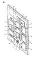
図1は本発明の第1の実施形態に係るインターポーザーとして使用することのできる半導体モジュールの斜視図である。半導体基板1の平坦な矩形の平板状のもので、平坦性、耐熱性に優れている必要があり、またICチップ等の電子部品の搭載性に優れている必要があることから、本発明ではシリコン基板を用いる。シリコン基板1自体の比誘電率は10程度である。
【0015】
このシリコン基板1表面上の一部の領域、即ち図1において矩形状の基板1の右側の短辺側に沿った縦長の矩形状の領域に強誘電体層2が形成され、この強誘電体層2上に導体膜から成るアンテナ3が形成される。
【0016】
強誘電体層2としては、例えばPZTを使用している。PZTは、チタン酸ジルコン酸鉛Pb(ZrxTi1 −x)O3 の混合セラミックであり、比誘電率は1200程度である。
【0017】
アンテナ3はその平面形状がF形状であり、アンテナ長さLは1.2mm以下と短く、また幅Wも1mm以下と短い。このアンテナ3への給電は、この基板1及び強誘電体層2上に形成された電源パターン4を通じて行われる。
【0018】
基板1の強誘電体層2の形成されている領域以外の領域には、複数個の半導体シリコンチップ5、インダクタンス6、キャパシタ7、SAWフィルタ8等の電子回路部品が形成されており、これらの電子部品がシリコン基板1と一体的に組み込まれていて、1つのマルチチップモジュール(MCM)を構成している。例えば、インダクタンス6のような電子回路部品については、従来は、部品としてのインダクタンスを基板上に実装するものが主流であったが、本実施形態では、シリコン基板1の表面に一体的に作り込む形態をとっている。
【0019】
シリコン基板1にはその表裏面を貫通するスルーホール9が多数形成されている。スルーホール9は、図では見えないが、多数のチップ5の下面にも形成されている。スルーホール9は、シリコン基板1上に形成されたアンテナ3や半導体シリコンチップ5、インダクタンス6、キャパシタ7、SAWフィルタ8等の電子回路部品に接続されている回路パターン10に接続され、図示しない基板裏面の回路パターンとの間で電気的の導通をとり、電源用、接地用或いは信号用配線の引き回しの便宜を図っている。
【0020】
図2は図1に示した半導体モジュールのスルーホール部分の断面図を示す。シリコン基板1にはレーザ加工、ドリル加工等により予め多数のスルーホール9が基板1の表裏面を貫通するように形成されている。シリコン基板1の表裏面及びスルーホール9の壁面には、例えばシリコン基板を熱酸化することにより形成した酸化シリコン(SiO2)等からなる絶縁膜11が形成されている。そして、この絶縁膜11上に必要な導体パッド12、導体パターン10等が形成されている。シリコン基板1の表裏面及びスルーホール9内壁の絶縁層上で導体層や導体パターンを形成するには、例えば、化学蒸着(CVD)、無電解めっき等によって形成したニッケル上に銅の電解めっき等を施すことにより形成することができる。
【0021】
図2に示すスルーホール9では、絶縁膜10の上に、下層配線であるグランド層12が形成され、その上に更に酸化シリコン(SiO2)等からなる絶縁膜13が形成され、その絶縁膜13上に表層としての信号層14が形成されている。そして、これらのスルーホール9内のグランド層12や信号層14はシリコン基板1の表裏面に形成されているグランドパターン(下層配線)15や信号パターン16にそれぞれ接続されている。
【0022】
外部接続のための端子としては、例えば導体パッド17上に半田バンプ18が形成されている。導体パッド17は、図2に示すように、例えばシリコン基板1の表裏面の信号パターン16に接続され、スルーホールの信号層14を介して基板1の反対面の信号パターンに接続される。このように、本実施形態では、例えばワイヤボンディング等のシールドワイヤを使用せずに、スルーホール等により導体間の接続を行なっているので、アンテナに対してノイズ等の影響を与えることがなくなる。
【0023】
図3は図1に示した半導体モジュールのシリコン基板1上に作り込むインダクタンスの一例を平面図で示したものである。このようなコイル状のインダクタンス6は例えば銅等の導体膜を化学エッチングすることにより形成することができる。
【0024】
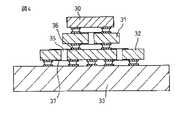
図4は本発明の第2の実施形態に係る半導体モジュールを示すもので、図1で説明したような基板をインターポーザーとして使用するに適したものである。図4において、電子部品として例えばチップコンデンサー(デカップリングコンデンサー)を搭載する場合について説明している。チップコンデンサー30は、別のチップコンデンサー又はインターポーザー31上にフリップチップ接合により搭載されている。このチップコンデンサー又はインターポーザー31は上述したようなスルーホール35を有する。このシリコンチップ又はインターポーザー31は更に別のチップコンデンサー又はインターポーザー32上にフリップチップ接合により搭載されている。このチップコンデンサー又はインターポーザー32にもまた上述したようなスルーホールが設けられている。そしてチップコンデンサー又はインターポーザー32はプリント基板又はパッケージ33上に同様にフリップチップ接合により搭載されている。図4において、36はフリップチップ接合用の導体パッドであり、37は再配線である。
【0025】
図5は本発明の第3の実施形態に係る半導体モジュールを示すもので、図4に示した第2の実施形態の場合と同様、基板をインターポーザーとして使用したものである。図4と異なる点は、中間にあるシリコンチップまたはインターポーザー31を省略し、電子部品としてのチップコンデンサー(デカップリングコンデンサー)30を別のシリコンチップ32上にフリップチップ接合により搭載した点である。このシリコンチップ32にもまた上述したようなスルーホールが設けられている。そしてシリコンチップ32はプリント基板又はパッケージ33上に前述と同様にフリップチップ接合により搭載されている。
【0026】
以上添付図面を参照して本発明の実施形態について詳細に説明したが、本発明は上記の実施形態に限定されるものではなく、本発明の精神ないし範囲内において種々の形態、変形、修正等が可能であることは言うまでもない。
【0027】
【発明の効果】
以上説明したように、本発明によれば、アンテナをコンパクトにし、またシリコンチップ(シリコンインターボーザー)に作り込むため、通信装置を非常に小さくすることができる。また、キャパシタ又はSAWフィルタ、インダクタンス等の電子部品をアンテナの形成と同時にインターポーザー上に形成することができ、低価格なマルチチップモジュール(MCM)を作製することができる。
【図面の簡単な説明】
【図1】本発明の第1の実施形態に係るインターポーザーとして使用することのできる半導体モジュールの斜視図である。
【図2】図1に示した半導体モジュールのスルーホール部分の断面図を示す。
【図3】本発明の半導体モジュール上に形成することの出来る電子部品の一例としてインダクタンスの平面図である。
【図4】本発明の第2の実施形態に係る半導体モジュールの断面図である。
【図5】本発明の第3の実施形態に係る半導体モジュールの断面図である。
【符号の説明】
1…シリコン基板
2…強誘電体膜
3…アンテナ
4…電源用配線
5…シリコンチップ
6…インダクタンス
7…キャパシタ
8…SAWフィルタ
9…スルーホール
10…導体パターン
11、13…絶縁膜
12…グランド配線
16…信号配線
17…パッド
18…半田バンプ[0001]
TECHNICAL FIELD OF THE INVENTION
The present invention relates to a structure of a semiconductor module that can function as an interposer and a method for manufacturing the same. In particular, the present invention can be applied to the manufacture of a multi-chip module using an interposer.
[0002]
[Prior art]
2. Description of the Related Art Conventionally, an antenna used for wireless communication or the like is usually manufactured using a conductor or a ceramic and a conductor, but the antenna structure is limited by a radio frequency. For example, when wireless communication in the 2.5 GHz band is performed using an antenna formed on a printed board made of ordinary glass epoxy (with a relative dielectric constant of about 4.5), an antenna length of 18 mm is required. On the other hand, when an antenna is formed on a ceramic substrate (relative permittivity 10), the antenna length needs to be about 13 mm.
[0003]
Even if it is attempted to apply a material having a high dielectric constant to the ceramic or printed circuit board forming the antenna, it is rare that the material used for these materials generally has a relative dielectric constant exceeding 100.
[0004]
As a conventional technique, a millimeter wave detector is disclosed in Japanese Patent Application Laid-Open No. 8-56113. In this prior art, a ground conductor film and a dielectric film are laminated on a semiconductor substrate made of silicon or gallium arsenide, and a planar antenna and a microstrip line for feeding power to the planar antenna are formed on the dielectric film. A second semiconductor substrate made of gallium arsenide provided with a circuit for detecting a signal or a circuit for generating a signal is mounted on a microstrip line by flip chip.
[0005]
Further, in this prior art, instead of forming a planar antenna on the dielectric film on a semiconductor substrate, a dielectric substrate is used, and power is supplied to the planar antenna formed on the substrate through a through hole. Also shown is a structure performed by terminals provided on the back surface of the substrate.
[0006]
[Problems to be solved by the invention]
As described above, in the case of forming an antenna for performing wireless communication on a printed circuit board, conventionally, since a certain length of the antenna is required, for example, it is not possible to form the antenna by incorporating the antenna in a silicon chip. This was impossible because a sufficient area for forming the antenna could not be secured.
[0007]
Therefore, in the present invention, a semiconductor module structure in which the length of the antenna can be shortened by improving the material of the module structure forming the antenna, so that the antenna can be formed in a silicon chip, for example, is provided. The task is to provide.
[0008]
[Means for Solving the Problems]
According to the present invention, there is provided a semiconductor module having a ferroelectric layer formed on a silicon substrate and an antenna formed on the ferroelectric layer. By forming the antenna on the ferroelectric layer on the silicon substrate in this manner, the antenna length can be reduced to 1.2 mm or less.
[0009]
As the ferroelectric used here, for example, zirconate titanate (PZT) is suitable. PZT is a lead zirconate titanate is a mixed ceramic ofPb (ZrxTi 1 -x) O 3 , a relative dielectric constant is about 1200. Therefore, even if the relative permittivity of the silicon substrate itself is about 10, the antenna length can be extremely reduced to 1.2 mm or less by forming a ferroelectric layer thereon and forming an antenna.
[0010]
An electronic element such as a capacitor or a SAW filter and an inductance is formed on the silicon substrate on which the antenna is formed, and the electronic element is incorporated in the module. As a result, electronic components having various functions in addition to the antenna function can be mounted in one module structure.
[0011]
Further, a through hole is formed in the silicon substrate on which the antenna is formed, a conductor layer is formed on a wall surface of the through hole via an insulating layer, and the conductor layer is connected to conductor patterns on the front and back surfaces of the silicon substrate. Features. In this manner, by providing the silicon substrate itself with the through holes penetrating the front and back surfaces, conduction of the pattern between the front and back surfaces of the substrate can be achieved.
[0012]
In this case, a ground layer is formed below a wall surface of the through hole via a first insulating layer, and a signal layer is formed on a top surface of the ground layer via a second insulating layer. Are connected to the ground layer and the signal pattern on the front and back surfaces of the silicon substrate, respectively.
[0013]
BEST MODE FOR CARRYING OUT THE INVENTION
Hereinafter, embodiments of the present invention will be described in detail with reference to the accompanying drawings.
[0014]
FIG. 1 is a perspective view of a semiconductor module that can be used as an interposer according to the first embodiment of the present invention. In the present invention, the semiconductor substrate 1 is required to have a flat rectangular flat plate shape and to have excellent flatness and heat resistance, and to have excellent mountability of electronic components such as IC chips. A silicon substrate is used. The relative permittivity of the silicon substrate 1 itself is about 10.
[0015]
A ferroelectric layer 2 is formed in a partial area on the surface of the silicon substrate 1, that is, a vertically long rectangular area along the short side on the right side of the rectangular substrate 1 in FIG. An antenna 3 made of a conductive film is formed on the layer 2.
[0016]
As the ferroelectric layer 2, for example, PZT is used. PZT is a mixed ceramic of lead zirconate titanatePb (ZrxTi 1 -x) O 3 , a relative dielectric constant is about 1200.
[0017]
The antenna 3 has an F-shaped planar shape, and the antenna length L is as short as 1.2 mm or less, and the width W is as short as 1 mm or less. Power is supplied to the antenna 3 through a power supply pattern 4 formed on the substrate 1 and the ferroelectric layer 2.
[0018]
In a region other than the region where the ferroelectric layer 2 of the substrate 1 is formed, a plurality of electronic circuit components such as a
[0019]
A large number of through
[0020]
FIG. 2 is a sectional view of a through-hole portion of the semiconductor module shown in FIG. A large number of through
[0021]
In the through
[0022]
As terminals for external connection, for example, solder bumps 18 are formed on the
[0023]
FIG. 3 is a plan view showing an example of an inductance formed on the silicon substrate 1 of the semiconductor module shown in FIG. Such a
[0024]
FIG. 4 shows a semiconductor module according to a second embodiment of the present invention, which is suitable for using the substrate described in FIG. 1 as an interposer. FIG. 4 illustrates a case where, for example, a chip capacitor (decoupling capacitor) is mounted as an electronic component. The
[0025]
FIG. 5 shows a semiconductor module according to a third embodiment of the present invention, in which a substrate is used as an interposer, as in the case of the second embodiment shown in FIG. The difference from FIG. 4 is that the silicon chip or the
[0026]
Although the embodiments of the present invention have been described in detail with reference to the accompanying drawings, the present invention is not limited to the above embodiments, and various forms, modifications, modifications, and the like are within the spirit and scope of the present invention. Needless to say, this is possible.
[0027]
【The invention's effect】
As described above, according to the present invention, since the antenna is made compact and built into a silicon chip (silicon interposer), the communication device can be made very small. In addition, electronic components such as a capacitor, a SAW filter, and an inductance can be formed on the interposer at the same time as the formation of the antenna, so that a low-cost multi-chip module (MCM) can be manufactured.
[Brief description of the drawings]
FIG. 1 is a perspective view of a semiconductor module that can be used as an interposer according to a first embodiment of the present invention.
FIG. 2 is a sectional view of a through-hole portion of the semiconductor module shown in FIG. 1;
FIG. 3 is a plan view of inductance as an example of an electronic component that can be formed on the semiconductor module of the present invention.
FIG. 4 is a sectional view of a semiconductor module according to a second embodiment of the present invention.
FIG. 5 is a sectional view of a semiconductor module according to a third embodiment of the present invention.
[Explanation of symbols]
DESCRIPTION OF SYMBOLS 1 ... Silicon substrate 2 ... Ferroelectric film 3 ... Antenna 4 ...
Claims (5)
Translated fromJapanesePriority Applications (6)
| Application Number | Priority Date | Filing Date | Title |
|---|---|---|---|
| JP2002173067AJP4010881B2 (en) | 2002-06-13 | 2002-06-13 | Semiconductor module structure |
| US10/448,219US20030230797A1 (en) | 2002-06-13 | 2003-05-30 | Semiconductor module structure incorporating antenna |
| EP03291348AEP1372215A3 (en) | 2002-06-13 | 2003-06-05 | Semiconductor module structure incorporating antenna |
| CNA03141317XACN1479407A (en) | 2002-06-13 | 2003-06-10 | Structure of a semiconductor component incorporating an antenna |
| TW092115828ATW200403885A (en) | 2002-06-13 | 2003-06-11 | Semiconductor module structure incorporating antenna |
| KR10-2003-0037879AKR20030096055A (en) | 2002-06-13 | 2003-06-12 | Semiconductor module structure incorporating antenna |
Applications Claiming Priority (1)
| Application Number | Priority Date | Filing Date | Title |
|---|---|---|---|
| JP2002173067AJP4010881B2 (en) | 2002-06-13 | 2002-06-13 | Semiconductor module structure |
Publications (2)
| Publication Number | Publication Date |
|---|---|
| JP2004022667Atrue JP2004022667A (en) | 2004-01-22 |
| JP4010881B2 JP4010881B2 (en) | 2007-11-21 |
Family
ID=29561801
Family Applications (1)
| Application Number | Title | Priority Date | Filing Date |
|---|---|---|---|
| JP2002173067AExpired - LifetimeJP4010881B2 (en) | 2002-06-13 | 2002-06-13 | Semiconductor module structure |
Country Status (6)
| Country | Link |
|---|---|
| US (1) | US20030230797A1 (en) |
| EP (1) | EP1372215A3 (en) |
| JP (1) | JP4010881B2 (en) |
| KR (1) | KR20030096055A (en) |
| CN (1) | CN1479407A (en) |
| TW (1) | TW200403885A (en) |
Cited By (4)
| Publication number | Priority date | Publication date | Assignee | Title |
|---|---|---|---|---|
| JP2007036571A (en)* | 2005-07-26 | 2007-02-08 | Shinko Electric Ind Co Ltd | Semiconductor device and its manufacturing method |
| JP2008263263A (en)* | 2007-04-10 | 2008-10-30 | Shinko Electric Ind Co Ltd | Antenna element and semiconductor device |
| JP2010206328A (en)* | 2009-02-27 | 2010-09-16 | Dainippon Printing Co Ltd | Electronic apparatus and electronic device |
| US8035192B2 (en) | 2007-12-27 | 2011-10-11 | Shinko Electric Industries Co., Ltd. | Semiconductor device and manufacturing method thereof |
Families Citing this family (6)
| Publication number | Priority date | Publication date | Assignee | Title |
|---|---|---|---|---|
| DE102004005666B4 (en)* | 2004-02-05 | 2008-05-29 | Infineon Technologies Ag | High frequency arrangement, method for producing a high frequency arrangement and use of the high frequency arrangement |
| JP2008541039A (en)* | 2005-05-04 | 2008-11-20 | エヌエックスピー ビー ヴィ | Device comprising a sensor module |
| US20070070608A1 (en)* | 2005-09-29 | 2007-03-29 | Skyworks Solutions, Inc. | Packaged electronic devices and process of manufacturing same |
| US7977155B2 (en)* | 2007-05-04 | 2011-07-12 | Taiwan Semiconductor Manufacturing Company, Ltd. | Wafer-level flip-chip assembly methods |
| US20140306349A1 (en)* | 2013-04-11 | 2014-10-16 | Qualcomm Incorporated | Low cost interposer comprising an oxidation layer |
| US10566686B2 (en)* | 2018-06-28 | 2020-02-18 | Micron Technology, Inc. | Stacked memory package incorporating millimeter wave antenna in die stack |
Family Cites Families (11)
| Publication number | Priority date | Publication date | Assignee | Title |
|---|---|---|---|---|
| DE4041271C2 (en)* | 1989-12-25 | 1998-10-08 | Toshiba Kawasaki Kk | Semiconductor device with a ferroelectric capacitor |
| JP2840493B2 (en)* | 1991-12-27 | 1998-12-24 | 株式会社日立製作所 | Integrated microwave circuit |
| JPH07333199A (en)* | 1994-06-13 | 1995-12-22 | Tokyo Gas Co Ltd | Micro eddy current sensor |
| US5970393A (en)* | 1997-02-25 | 1999-10-19 | Polytechnic University | Integrated micro-strip antenna apparatus and a system utilizing the same for wireless communications for sensing and actuation purposes |
| ATE434259T1 (en)* | 1997-10-14 | 2009-07-15 | Patterning Technologies Ltd | METHOD OF MAKING AN ELECTRICAL CAPACITOR |
| US6329915B1 (en)* | 1997-12-31 | 2001-12-11 | Intermec Ip Corp | RF Tag having high dielectric constant material |
| US6329959B1 (en)* | 1999-06-17 | 2001-12-11 | The Penn State Research Foundation | Tunable dual-band ferroelectric antenna |
| US6292143B1 (en)* | 2000-05-04 | 2001-09-18 | The United States Of America As Represented By The Administrator Of The National Aeronautics And Space Administration | Multi-mode broadband patch antenna |
| US6529088B2 (en)* | 2000-12-26 | 2003-03-04 | Vistar Telecommunications Inc. | Closed loop antenna tuning system |
| US6607394B2 (en)* | 2001-02-06 | 2003-08-19 | Optillion Ab | Hot-pluggable electronic component connection |
| US6690251B2 (en)* | 2001-04-11 | 2004-02-10 | Kyocera Wireless Corporation | Tunable ferro-electric filter |
- 2002
- 2002-06-13JPJP2002173067Apatent/JP4010881B2/ennot_activeExpired - Lifetime
- 2003
- 2003-05-30USUS10/448,219patent/US20030230797A1/ennot_activeAbandoned
- 2003-06-05EPEP03291348Apatent/EP1372215A3/ennot_activeWithdrawn
- 2003-06-10CNCNA03141317XApatent/CN1479407A/enactivePending
- 2003-06-11TWTW092115828Apatent/TW200403885A/enunknown
- 2003-06-12KRKR10-2003-0037879Apatent/KR20030096055A/ennot_activeCeased
Cited By (6)
| Publication number | Priority date | Publication date | Assignee | Title |
|---|---|---|---|---|
| JP2007036571A (en)* | 2005-07-26 | 2007-02-08 | Shinko Electric Ind Co Ltd | Semiconductor device and its manufacturing method |
| US7569924B2 (en) | 2005-07-26 | 2009-08-04 | Shinko Electric Industries Co., Ltd. | Semiconductor device and manufacturing method thereof |
| JP2008263263A (en)* | 2007-04-10 | 2008-10-30 | Shinko Electric Ind Co Ltd | Antenna element and semiconductor device |
| US8018392B2 (en) | 2007-04-10 | 2011-09-13 | Shinko Electric Industries Co., Ltd. | Antenna element and semiconductor device |
| US8035192B2 (en) | 2007-12-27 | 2011-10-11 | Shinko Electric Industries Co., Ltd. | Semiconductor device and manufacturing method thereof |
| JP2010206328A (en)* | 2009-02-27 | 2010-09-16 | Dainippon Printing Co Ltd | Electronic apparatus and electronic device |
Also Published As
| Publication number | Publication date |
|---|---|
| JP4010881B2 (en) | 2007-11-21 |
| EP1372215A3 (en) | 2004-04-07 |
| EP1372215A2 (en) | 2003-12-17 |
| US20030230797A1 (en) | 2003-12-18 |
| KR20030096055A (en) | 2003-12-24 |
| TW200403885A (en) | 2004-03-01 |
| CN1479407A (en) | 2004-03-03 |
Similar Documents
| Publication | Publication Date | Title |
|---|---|---|
| US5717249A (en) | RF power amplifying circuit device | |
| US6362525B1 (en) | Circuit structure including a passive element formed within a grid array substrate and method for making the same | |
| JP3890947B2 (en) | High frequency semiconductor device | |
| US8034664B2 (en) | Method of fabricating passive device applied to the three-dimensional package module | |
| US7236373B2 (en) | Electronic device capable of preventing electromagnetic wave from being radiated | |
| US7884458B2 (en) | Decoupling capacitor, wafer stack package including the decoupling capacitor, and method of fabricating the wafer stack package | |
| KR101414751B1 (en) | Capacitor embedded substrate and manufacturing method thereof | |
| US20090267221A1 (en) | Semiconductor device | |
| US20080315396A1 (en) | Mold compound circuit structure for enhanced electrical and thermal performance | |
| JP4979213B2 (en) | Circuit board, circuit board manufacturing method, and circuit device | |
| JP2004079701A (en) | Semiconductor device and its manufacturing method | |
| TW201946245A (en) | Semiconductor packages and apparatus having the same | |
| JP3443408B2 (en) | Wiring board and semiconductor device using the same | |
| JP4010881B2 (en) | Semiconductor module structure | |
| JPH08335836A (en) | High frequency power amplifier circuit device | |
| JP3081786B2 (en) | High frequency semiconductor device | |
| JPH09148373A (en) | Radio communication module | |
| US20070013079A1 (en) | Die pad arrangement and bumpless chip package applying the same | |
| JPH11354667A (en) | Electronic component and its mounting method | |
| JP2005340713A (en) | Multichip module | |
| TWI778654B (en) | Electronic package and manufacturing method thereof | |
| KR100632237B1 (en) | 3D multilayer multichip module package manufacturing method | |
| JP3831173B2 (en) | Semiconductor module | |
| TW200421567A (en) | Semiconductor device | |
| JPH04137691A (en) | circuit board |
Legal Events
| Date | Code | Title | Description |
|---|---|---|---|
| A621 | Written request for application examination | Free format text:JAPANESE INTERMEDIATE CODE: A621 Effective date:20050127 | |
| A131 | Notification of reasons for refusal | Free format text:JAPANESE INTERMEDIATE CODE: A131 Effective date:20070515 | |
| A521 | Request for written amendment filed | Free format text:JAPANESE INTERMEDIATE CODE: A523 Effective date:20070703 | |
| TRDD | Decision of grant or rejection written | ||
| A01 | Written decision to grant a patent or to grant a registration (utility model) | Free format text:JAPANESE INTERMEDIATE CODE: A01 Effective date:20070807 | |
| A61 | First payment of annual fees (during grant procedure) | Free format text:JAPANESE INTERMEDIATE CODE: A61 Effective date:20070904 | |
| R150 | Certificate of patent or registration of utility model | Ref document number:4010881 Country of ref document:JP Free format text:JAPANESE INTERMEDIATE CODE: R150 Free format text:JAPANESE INTERMEDIATE CODE: R150 | |
| FPAY | Renewal fee payment (event date is renewal date of database) | Free format text:PAYMENT UNTIL: 20100914 Year of fee payment:3 | |
| FPAY | Renewal fee payment (event date is renewal date of database) | Free format text:PAYMENT UNTIL: 20110914 Year of fee payment:4 | |
| FPAY | Renewal fee payment (event date is renewal date of database) | Free format text:PAYMENT UNTIL: 20110914 Year of fee payment:4 | |
| FPAY | Renewal fee payment (event date is renewal date of database) | Free format text:PAYMENT UNTIL: 20120914 Year of fee payment:5 | |
| FPAY | Renewal fee payment (event date is renewal date of database) | Free format text:PAYMENT UNTIL: 20120914 Year of fee payment:5 | |
| FPAY | Renewal fee payment (event date is renewal date of database) | Free format text:PAYMENT UNTIL: 20130914 Year of fee payment:6 | |
| EXPY | Cancellation because of completion of term |