JP2004006819A - Method for manufacturing semiconductor device - Google Patents
Method for manufacturing semiconductor deviceDownload PDFInfo
- Publication number
- JP2004006819A JP2004006819AJP2003112438AJP2003112438AJP2004006819AJP 2004006819 AJP2004006819 AJP 2004006819AJP 2003112438 AJP2003112438 AJP 2003112438AJP 2003112438 AJP2003112438 AJP 2003112438AJP 2004006819 AJP2004006819 AJP 2004006819A
- Authority
- JP
- Japan
- Prior art keywords
- film
- chemical solution
- oxide film
- cleaning
- semiconductor substrate
- Prior art date
- Legal status (The legal status is an assumption and is not a legal conclusion. Google has not performed a legal analysis and makes no representation as to the accuracy of the status listed.)
- Pending
Links
- 239000004065semiconductorSubstances0.000titleclaimsabstractdescription87
- 238000000034methodMethods0.000titleclaimsabstractdescription43
- 238000004519manufacturing processMethods0.000titleclaimsabstractdescription21
- 239000000126substanceSubstances0.000claimsabstractdescription137
- 239000000243solutionSubstances0.000claimsabstractdescription106
- 239000000758substrateSubstances0.000claimsabstractdescription101
- 229910000577Silicon-germaniumInorganic materials0.000claimsabstractdescription95
- QGZKDVFQNNGYKY-UHFFFAOYSA-NammoniaNatural productsNQGZKDVFQNNGYKY-UHFFFAOYSA-N0.000claimsabstractdescription77
- KRHYYFGTRYWZRS-UHFFFAOYSA-NFluoraneChemical compoundFKRHYYFGTRYWZRS-UHFFFAOYSA-N0.000claimsabstractdescription38
- 238000001312dry etchingMethods0.000claimsabstractdescription25
- VHUUQVKOLVNVRT-UHFFFAOYSA-NAmmonium hydroxideChemical compound[NH4+].[OH-]VHUUQVKOLVNVRT-UHFFFAOYSA-N0.000claimsabstractdescription24
- 239000011259mixed solutionSubstances0.000claimsabstractdescription24
- 238000000059patterningMethods0.000claimsabstractdescription20
- 229910052710siliconInorganic materials0.000claimsabstractdescription13
- 238000004140cleaningMethods0.000claimsdescription91
- MHAJPDPJQMAIIY-UHFFFAOYSA-NHydrogen peroxideChemical compoundOOMHAJPDPJQMAIIY-UHFFFAOYSA-N0.000claimsdescription73
- 229910021529ammoniaInorganic materials0.000claimsdescription36
- 235000011114ammonium hydroxideNutrition0.000claimsdescription23
- 229910021420polycrystalline siliconInorganic materials0.000claimsdescription19
- 229910000040hydrogen fluorideInorganic materials0.000claimsdescription4
- 239000002245particleSubstances0.000abstractdescription43
- XLYOFNOQVPJJNP-UHFFFAOYSA-NwaterSubstancesOXLYOFNOQVPJJNP-UHFFFAOYSA-N0.000abstractdescription25
- 238000005406washingMethods0.000abstractdescription10
- 239000010410layerSubstances0.000description73
- 238000005530etchingMethods0.000description35
- 239000000203mixtureSubstances0.000description28
- 239000007788liquidSubstances0.000description21
- 238000012545processingMethods0.000description17
- 239000007921spraySubstances0.000description12
- 239000004020conductorSubstances0.000description10
- 238000001035dryingMethods0.000description10
- VYPSYNLAJGMNEJ-UHFFFAOYSA-NSilicium dioxideChemical compoundO=[Si]=OVYPSYNLAJGMNEJ-UHFFFAOYSA-N0.000description9
- 229910052814silicon oxideInorganic materials0.000description9
- QAOWNCQODCNURD-UHFFFAOYSA-NSulfuric acidChemical compoundOS(O)(=O)=OQAOWNCQODCNURD-UHFFFAOYSA-N0.000description8
- 230000000694effectsEffects0.000description7
- 239000012535impuritySubstances0.000description6
- XUIMIQQOPSSXEZ-UHFFFAOYSA-NSiliconChemical compound[Si]XUIMIQQOPSSXEZ-UHFFFAOYSA-N0.000description5
- 239000010703siliconSubstances0.000description5
- 238000010129solution processingMethods0.000description5
- 230000007423decreaseEffects0.000description4
- QOSATHPSBFQAML-UHFFFAOYSA-Nhydrogen peroxide;hydrateChemical compoundO.OOQOSATHPSBFQAML-UHFFFAOYSA-N0.000description4
- 238000002955isolationMethods0.000description4
- 239000007789gasSubstances0.000description3
- 238000000206photolithographyMethods0.000description3
- 229920002120photoresistant polymerPolymers0.000description3
- 238000003860storageMethods0.000description3
- 239000000654additiveSubstances0.000description2
- 230000000996additive effectEffects0.000description2
- 229910052787antimonyInorganic materials0.000description2
- 229910052785arsenicInorganic materials0.000description2
- 230000015572biosynthetic processEffects0.000description2
- 238000005229chemical vapour depositionMethods0.000description2
- 238000000151depositionMethods0.000description2
- 230000008021depositionEffects0.000description2
- 238000007598dipping methodMethods0.000description2
- 238000005516engineering processMethods0.000description2
- 230000001771impaired effectEffects0.000description2
- 239000011261inert gasSubstances0.000description2
- 238000009413insulationMethods0.000description2
- 238000002156mixingMethods0.000description2
- 229910052698phosphorusInorganic materials0.000description2
- 238000005507sprayingMethods0.000description2
- DDFHBQSCUXNBSA-UHFFFAOYSA-N5-(5-carboxythiophen-2-yl)thiophene-2-carboxylic acidChemical compoundS1C(C(=O)O)=CC=C1C1=CC=C(C(O)=O)S1DDFHBQSCUXNBSA-UHFFFAOYSA-N0.000description1
- NLXLAEXVIDQMFP-UHFFFAOYSA-NAmmonium chlorideSubstances[NH4+].[Cl-]NLXLAEXVIDQMFP-UHFFFAOYSA-N0.000description1
- IJGRMHOSHXDMSA-UHFFFAOYSA-NAtomic nitrogenChemical compoundN#NIJGRMHOSHXDMSA-UHFFFAOYSA-N0.000description1
- PXGOKWXKJXAPGV-UHFFFAOYSA-NFluorineChemical compoundFFPXGOKWXKJXAPGV-UHFFFAOYSA-N0.000description1
- SWXQKHHHCFXQJF-UHFFFAOYSA-Nazane;hydrogen peroxideChemical compound[NH4+].[O-]OSWXQKHHHCFXQJF-UHFFFAOYSA-N0.000description1
- 239000005380borophosphosilicate glassSubstances0.000description1
- 230000005587bubblingEffects0.000description1
- 238000012993chemical processingMethods0.000description1
- 238000006243chemical reactionMethods0.000description1
- 230000006866deteriorationEffects0.000description1
- 229910001873dinitrogenInorganic materials0.000description1
- 238000007599dischargingMethods0.000description1
- 238000004090dissolutionMethods0.000description1
- 229910052731fluorineInorganic materials0.000description1
- 239000011737fluorineSubstances0.000description1
- 239000011229interlayerSubstances0.000description1
- 238000005468ion implantationMethods0.000description1
- 238000010030laminatingMethods0.000description1
- 239000000463materialSubstances0.000description1
- 230000008018meltingEffects0.000description1
- 238000002844meltingMethods0.000description1
- 239000002184metalSubstances0.000description1
- 229910052751metalInorganic materials0.000description1
- 230000003647oxidationEffects0.000description1
- 238000007254oxidation reactionMethods0.000description1
- 229920005591polysiliconPolymers0.000description1
- 238000001039wet etchingMethods0.000description1
Images


Classifications
- H—ELECTRICITY
- H01—ELECTRIC ELEMENTS
- H01L—SEMICONDUCTOR DEVICES NOT COVERED BY CLASS H10
- H01L21/00—Processes or apparatus adapted for the manufacture or treatment of semiconductor or solid state devices or of parts thereof
- H01L21/02—Manufacture or treatment of semiconductor devices or of parts thereof
- H01L21/02041—Cleaning
- H01L21/02057—Cleaning during device manufacture
- H01L21/02068—Cleaning during device manufacture during, before or after processing of conductive layers, e.g. polysilicon or amorphous silicon layers
- H01L21/02071—Cleaning during device manufacture during, before or after processing of conductive layers, e.g. polysilicon or amorphous silicon layers the processing being a delineation, e.g. RIE, of conductive layers
- H—ELECTRICITY
- H01—ELECTRIC ELEMENTS
- H01L—SEMICONDUCTOR DEVICES NOT COVERED BY CLASS H10
- H01L21/00—Processes or apparatus adapted for the manufacture or treatment of semiconductor or solid state devices or of parts thereof
- H01L21/02—Manufacture or treatment of semiconductor devices or of parts thereof
- H01L21/02041—Cleaning
- H01L21/02057—Cleaning during device manufacture
- H01L21/0206—Cleaning during device manufacture during, before or after processing of insulating layers
- H01L21/02063—Cleaning during device manufacture during, before or after processing of insulating layers the processing being the formation of vias or contact holes
- H—ELECTRICITY
- H01—ELECTRIC ELEMENTS
- H01L—SEMICONDUCTOR DEVICES NOT COVERED BY CLASS H10
- H01L21/00—Processes or apparatus adapted for the manufacture or treatment of semiconductor or solid state devices or of parts thereof
- H01L21/02—Manufacture or treatment of semiconductor devices or of parts thereof
- H01L21/04—Manufacture or treatment of semiconductor devices or of parts thereof the devices having potential barriers, e.g. a PN junction, depletion layer or carrier concentration layer
- H01L21/18—Manufacture or treatment of semiconductor devices or of parts thereof the devices having potential barriers, e.g. a PN junction, depletion layer or carrier concentration layer the devices having semiconductor bodies comprising elements of Group IV of the Periodic Table or AIIIBV compounds with or without impurities, e.g. doping materials
- H01L21/28—Manufacture of electrodes on semiconductor bodies using processes or apparatus not provided for in groups H01L21/20 - H01L21/268
- H01L21/28008—Making conductor-insulator-semiconductor electrodes
- H01L21/28017—Making conductor-insulator-semiconductor electrodes the insulator being formed after the semiconductor body, the semiconductor being silicon
- H01L21/28026—Making conductor-insulator-semiconductor electrodes the insulator being formed after the semiconductor body, the semiconductor being silicon characterised by the conductor
- H01L21/2807—Making conductor-insulator-semiconductor electrodes the insulator being formed after the semiconductor body, the semiconductor being silicon characterised by the conductor the final conductor layer next to the insulator being Si or Ge or C and their alloys except Si
- H—ELECTRICITY
- H01—ELECTRIC ELEMENTS
- H01L—SEMICONDUCTOR DEVICES NOT COVERED BY CLASS H10
- H01L21/00—Processes or apparatus adapted for the manufacture or treatment of semiconductor or solid state devices or of parts thereof
- H01L21/02—Manufacture or treatment of semiconductor devices or of parts thereof
- H01L21/04—Manufacture or treatment of semiconductor devices or of parts thereof the devices having potential barriers, e.g. a PN junction, depletion layer or carrier concentration layer
- H01L21/18—Manufacture or treatment of semiconductor devices or of parts thereof the devices having potential barriers, e.g. a PN junction, depletion layer or carrier concentration layer the devices having semiconductor bodies comprising elements of Group IV of the Periodic Table or AIIIBV compounds with or without impurities, e.g. doping materials
- H01L21/30—Treatment of semiconductor bodies using processes or apparatus not provided for in groups H01L21/20 - H01L21/26
- H01L21/302—Treatment of semiconductor bodies using processes or apparatus not provided for in groups H01L21/20 - H01L21/26 to change their surface-physical characteristics or shape, e.g. etching, polishing, cutting
- H01L21/306—Chemical or electrical treatment, e.g. electrolytic etching
- H01L21/30604—Chemical etching
- H—ELECTRICITY
- H01—ELECTRIC ELEMENTS
- H01L—SEMICONDUCTOR DEVICES NOT COVERED BY CLASS H10
- H01L21/00—Processes or apparatus adapted for the manufacture or treatment of semiconductor or solid state devices or of parts thereof
- H01L21/02—Manufacture or treatment of semiconductor devices or of parts thereof
- H01L21/04—Manufacture or treatment of semiconductor devices or of parts thereof the devices having potential barriers, e.g. a PN junction, depletion layer or carrier concentration layer
- H01L21/18—Manufacture or treatment of semiconductor devices or of parts thereof the devices having potential barriers, e.g. a PN junction, depletion layer or carrier concentration layer the devices having semiconductor bodies comprising elements of Group IV of the Periodic Table or AIIIBV compounds with or without impurities, e.g. doping materials
- H01L21/30—Treatment of semiconductor bodies using processes or apparatus not provided for in groups H01L21/20 - H01L21/26
- H01L21/31—Treatment of semiconductor bodies using processes or apparatus not provided for in groups H01L21/20 - H01L21/26 to form insulating layers thereon, e.g. for masking or by using photolithographic techniques; After treatment of these layers; Selection of materials for these layers
- H01L21/3205—Deposition of non-insulating-, e.g. conductive- or resistive-, layers on insulating layers; After-treatment of these layers
- H01L21/321—After treatment
- H01L21/3213—Physical or chemical etching of the layers, e.g. to produce a patterned layer from a pre-deposited extensive layer
- H01L21/32133—Physical or chemical etching of the layers, e.g. to produce a patterned layer from a pre-deposited extensive layer by chemical means only
- H01L21/32135—Physical or chemical etching of the layers, e.g. to produce a patterned layer from a pre-deposited extensive layer by chemical means only by vapour etching only
- H01L21/32136—Physical or chemical etching of the layers, e.g. to produce a patterned layer from a pre-deposited extensive layer by chemical means only by vapour etching only using plasmas
- H01L21/32137—Physical or chemical etching of the layers, e.g. to produce a patterned layer from a pre-deposited extensive layer by chemical means only by vapour etching only using plasmas of silicon-containing layers
Landscapes
- Engineering & Computer Science (AREA)
- Physics & Mathematics (AREA)
- Microelectronics & Electronic Packaging (AREA)
- General Physics & Mathematics (AREA)
- Manufacturing & Machinery (AREA)
- Computer Hardware Design (AREA)
- Condensed Matter Physics & Semiconductors (AREA)
- Power Engineering (AREA)
- Chemical & Material Sciences (AREA)
- Chemical Kinetics & Catalysis (AREA)
- General Chemical & Material Sciences (AREA)
- Plasma & Fusion (AREA)
- Cleaning Or Drying Semiconductors (AREA)
- Weting (AREA)
Abstract
Description
Translated fromJapanese【0001】
【発明の属する技術分野】
本発明は、SiGe層を含むゲート電極を有する半導体装置の製造方法に関する。
【0002】
【従来の技術】
半導体装置の製造において、導電膜や絶縁膜のパターニングは、半導体基板上に形成した導電膜や絶縁膜上にレジスト膜を形成した後、フォトリソグラフィーによりレジストパターンを形成し、あるいはSiO2等からなるハードマスクパターンを形成し、これらのパターンをマスクとして導電膜や絶縁膜をエッチングすることにより行われている。その際、微細なパターンを形成するためには、通常ドライエッチングが行われる。しかしながら、ドライエッチングによりパターニングを行うと、ドライエッチ生成物やパーティクル等の異物が半導体基板上に付着する。このような異物が付着した状態のまま次の工程に移ると、製造における歩留りの低下や、素子特性および信頼性の低下を招く。そのため、パターニング後には半導体基板を洗浄し、基板に付着した異物を十分に除去する必要がある。
【0003】
絶縁膜のパターニング後に行う洗浄については、例えば半導体ウェハを薬液処理する半導体製造装置に関する特開平4−142741号公報に開示がある。同公報には、シリコン半導体ウェハ上のシリコン酸化膜を、フッ酸系の処理液(フッ酸とフッ化アンモニウムの混合液)を用いてウエットエッチングしてパターニングした後、硫酸と過酸化水素水との混合液で基板を処理してフォトレジストを除去し、続いてアンモニア水と過酸化水素水と純水との混合液を用いてウェハを洗浄してウェハ表面に付着したパーティクルを除去することが記載されている。また同公報には、ウェハの乾燥によってパーティクルがウェハ表面に強く固着し、除去が困難になることが記載されており、シリコン酸化膜のウエットエッチング後に連続してフォトレジストの除去およびパーティクルの除去処理を行うことにより、このような問題を解決することができることが記載されている。さらに同公報には、シリコン酸化膜のエッチング処理装置は、ポリシリコン膜のエッチング処理装置にも適用できることが記載されている。
【0004】
一方、導電膜のパターニング後に行う洗浄については、例えば特開2000−223464号公報に開示がある。同公報には、半導体基板上の高融点金属膜(WSi膜)と多結晶シリコン膜との積層膜をドライエッチングによりパターニングしてゲート電極を形成した後、液温35℃または45℃のアンモニア−過酸化水素水の混合液を用いて基板を洗浄し、基板上に堆積したエッチング残渣を除去することが記載されている。
【0005】
この特開2000−223464号公報には、アンモニア−過酸化水素水の混合液を用いて基板を長時間洗浄すると、ゲート電極を構成するWSi膜の側面の溶解が進み、膜減り部が発生することが記載されている。同公報では、このようなWSi膜の膜減り等を防止しつつドライエッチング残渣等の堆積物を実質的に完全に除去するために、ダミー基板を用いて決定した特定の処理時間で基板の洗浄を行うことが提案されている。また同公報には、ウエット処理に対するエッチングレートの異なる複数の絶縁膜(酸化シリコン膜、BPSG膜、BSG膜)からなる層間絶縁膜にドライエッチングにより接続孔を形成し、この接続孔の表面に付着したエッチング残渣をアンモニア−過酸化水素水の混合液を用いて洗浄することが記載されている。この洗浄においても、処理時間を長くしすぎるとエッチングレートの差により接続孔の内壁に凹凸が形成されるため、この凹凸の発生を防止しつつエッチング残渣を除去することを目的として、ダミー基板を用いて決定した特定の処理時間で洗浄を行うことが記載されている。
【0006】
【発明が解決しようとしている課題】
近年、素子の電気的特性を向上させる点から、SiGe層と多結晶シリコン層とからなるゲート電極を有する半導体装置が提案されている。例えば、Y.V.Ponomarev et al., IEDM’97, p.829には、下層が仕事関数を制御するためのSiGe層(poly−Si0.8Ge0.2)、上層が多結晶シリコン層(poly−Si)のゲート電極を有する半導体装置が提案されており、その素子特性についても詳細に記載されている。
【0007】
また、Wen−Chin Lee et al., 1998 Symposium on VLSI Technology Digest ofTechnical Papers, p.190には、PまたはBを導入したSiGe層(poly−Si1−xGex)からなるゲート電極を有する半導体装置が記載されている。Ja−Hum Ku et al., 2000 Symposium on VLSI Technology Digest of Technical Papers, p.114には、SiGe層(poly−Si0.8Ge0.2)上にNi/TiNを堆積し、アニールして形成したゲート電極(Ni(SixGe1−x)/poly−Si0.8Ge0.2)を有する半導体装置が記載されている。
【0008】
SiGe層と多結晶シリコン層とからなるゲートパターンは、半導体基板上に酸化膜、SiGe膜、多結晶シリコン膜をこの順で積層し、この積層膜上にレジスト膜を形成した後にフォトリソグラフィーによりレジストパターンを形成し、このレジストパターンをマスクとして積層膜をドライエッチングして形成される。しかし、このようにドライエッチングによりパターニングを行い、SiGe層と多結晶シリコン層とからなるゲート電極パターン及びゲート酸化膜パターンを形成した後には、エッチングガスと被エッチング対象物との化学反応により生成したドライエッチ生成物やパーティクルが半導体基板表面やゲート電極に付着する。そのため、半導体基板を洗浄してこれらの付着物を除去する必要がある。
【0009】
しかしながら、半導体基板やゲート電極に付着したドライエッチ生成物やパーティクルを除去するために、アンモニア水と過酸化水素水の混合液を用いた従来の洗浄方法により洗浄を行うと、SiGe層の側面が膜減りする(以下適宜「サイドエッチ」と表記する)という問題が生じる。
【0010】
図2を用いて、従来の洗浄方法の上記問題についてさらに説明する。図2(a)は洗浄前のゲート電極パターン及びゲート酸化膜パターン形成後の半導体基板の概略断面図であり、図2(b)は洗浄後の半導体基板の概略断面図である。図中、符号1は半導体基板、符号2はゲート酸化膜、符号3はSiGe層、符号4は多結晶シリコン層、符号5は素子分離領域を示す。
【0011】
前述の通り、SiGe膜を含む積層膜を、レジストパターンをマスクとしてドライエッチングすると(図2(a))、半導体基板表面やゲート電極にドライエッチ生成物やパーティクル(不図示)が付着する。このように半導体基板に付着したドライエッチ生成物やパーティクルを除去するためには、従来の洗浄方法に用いられているアンモニア水と過酸化水素水の混合液を用いることができるが、ドライエッチ生成物を十分に除去するためにはアンモニア濃度と液温とを高くすることが必要となる。これは、SiGe層に由来するドライエッチ生成物がこの混合液へ溶解しにくいためと考えられる。
【0012】
しかし、ドライエッチ生成物を十分に除去できるように、高温で高アンモニア濃度の混合液を用いて洗浄を行うと、図2(b)に示すように、SiGe層3がサイドエッチされる。これは、SiGe層がこの混合液に対して溶解性が高いためであり、特にSiGe層がGeを10原子%以上、さらには20原子%以上含有する場合に、このSiGe層のサイドエッチの問題がより顕著になってくる。このようなゲート電極のSiGe層のサイドエッチは、デバイス動作不良の原因となる。
【0013】
すなわち、洗浄に用いる薬液(洗浄液)としてアンモニア水と過酸化水素水の混合液を用いた従来の洗浄方法では、SiGe層のサイドエッチを防止しながら、半導体基板に付着したドライエッチ生成物やパーティクルを十分に除去することは非常に困難であった。加えて、良好な素子特性を得るためには、ゲート酸化膜にもダメージを与えないことが必要である。
【0014】
そこで本発明の目的は、Si及びGeを含有するSiGe膜と酸化膜とを有する積層膜をドライエッチングによりパターニングしてゲート電極パターン及びゲート酸化膜パターンを形成した後、ゲートを構成するSiGe層とゲート酸化膜とを損傷させることなく、半導体基板上に付着したドライエッチ生成物やパーティクルを十分に除去し、素子特性および信頼性に優れた半導体装置を歩留りよく製造することにある。
【0015】
【課題を解決するための手段】
本発明によれば、半導体基板上に、ゲート酸化膜と、Si及びGeを含有するSiGe層を含むゲート電極とを有する半導体装置の製造方法であって、
半導体基板上に、酸化膜と、Si及びGeを含有するSiGe膜とがこの順で形成された積層膜をドライエッチングしてゲート電極パターンおよび酸化膜パターンを形成するパターニング工程と、
前記パターニング工程の後、フッ化水素酸からなる第1の薬液を用いて、前記積層膜がパターニングされた半導体基板を洗浄する第1の洗浄工程と、
前記第1の洗浄工程の後、アンモニア水と過酸化水素水の混合液からなる第2の薬液を用いて前記半導体基板を洗浄する第2の洗浄工程とを有する半導体装置の製造方法が提供される。
【0016】
また本発明によれば、前記第2の薬液のアンモニア濃度が0.05〜1.5質量%であり、
前記第2の薬液中のアンモニアに対する過酸化水素の含有比率(質量基準)が1以上(過酸化水素/アンモニア)である半導体装置の製造方法が提供される。
【0017】
また本発明によれば、前記第2の洗浄工程において、前記第2の薬液の使用温度が45℃以下である半導体装置の製造方法が提供される。
【0018】
また本発明によれば、前記第1の薬液のフッ化水素濃度が0.05〜1.0質量%である半導体装置の製造方法が提供される。
【0019】
本発明では、酸化膜とSiGe膜とをこの順で有する積層膜をドライエッチングによりパターニングしてゲート電極パターン及びゲート酸化膜パターンを形成した後、半導体基板に付着したエッチング生成物およびパーティクルを除去するための洗浄を2段階で行う。すなわち、エッチング生成物の除去に適した第1の洗浄工程と、パーティクルの除去に適した第2の洗浄工程との2段階の洗浄を行う。これにより、各洗浄工程においてそれぞれ除去対象物に最適な薬液を用いることができ、優れた洗浄効果を得ることができる。さらに、除去対象物に対する薬液の洗浄効果が高いこと、及び、洗浄工程ごとに薬液の濃度や組成、洗浄条件を設定できることから、除去対象物に対する洗浄効果を十分に確保しつつ、SiGe層やゲート酸化膜に対する薬液の溶解性、すなわちSiGe層やゲート酸化膜のサイドエッチを十分に抑えることができる。
【0020】
本発明における第1の洗浄工程は、主にドライエッチ生成物を除去することを目的とし、フッ化水素酸からなる第1の薬液を用いて半導体基板を洗浄する。本発明者は、第1の薬液として用いられるフッ化水素酸は、パーティクルの除去力はそれほど高くはないが、ドライエッチ生成物の除去力が非常に高いことを見出した。一般にフッ化水素酸は酸化物の除去力が高いことが知られており、ゲート酸化膜が露出する状態で洗浄液に使用することはゲート酸化膜にダメージを与えやすい。しかしながら、フッ化水素酸はドライエッチ生成物の除去力が非常に高いため、低濃度にして酸化物の除去力を低下させても、ドライエッチ生成物を十分に除去できることを見出した。すなわち、本発明では、フッ化水素酸を第1の薬液として用いることにより、ゲート酸化膜のサイドエッチを十分に抑えつつ、ドライエッチ生成物を十分に除去することが可能である。また、フッ化水素酸からなる第1の薬液のSiGe層に対するエッチレートは低く、第1の洗浄工程においてSiGe層のサイドエッチが問題になることはない。
【0021】
本発明における第2の洗浄工程は、主にパーティクルを除去することを目的とし、アンモニア水と過酸化水素水の混合液からなる第2の薬液を用いて半導体基板を洗浄する。本発明者は、第2の薬液として用いられるアンモニア水と過酸化水素水の混合液は、ドライエッチ生成物の除去力はそれほど高くはないが、パーティクルの除去力が特定の組成範囲において非常に高いことを見出した。アンモニア水と過酸化水素水の混合液は洗浄液として一般に知られているが、従来の使用濃度ではSiGe層のエッチレートが非常に高く、第2の洗浄工程において用いるとパーティクルは十分に除去できるが、SiGe層のサイドエッチが生じてしまう。しかしながら、本発明者は、アンモニアと過酸化水素の含有比率が特定の範囲に制御されている限り、薬液の濃度を下げてSiGe層のエッチレートを低下させても、本発明において必要とされるパーティクルの除去力を十分に得ることができることを見出した。すなわち、本発明では、アンモニア水と過酸化水素水の混合液を第2の薬液として用いることにより、SiGe層のサイドエッチを十分に抑えつつ、パーティクルを十分に除去することが可能である。また、アンモニア水と過酸化水素水の混合液からなる第2の薬液のゲート酸化膜に対するエッチレートは低く、第2の洗浄工程においてゲート酸化膜のサイドエッチが問題になることはない。
【0022】
このように、本発明では、半導体基板上に酸化膜とSiGe膜とをこの順で有する積層膜をドライエッチングによりパターニングしてゲート電極パターン及びゲート酸化膜パターンを形成した後、主にドライエッチ生成物を除去するための第1の洗浄工程と、主にパーティクルを除去するための第2の洗浄工程とに分けて半導体基板を洗浄することによって、ゲート電極のSiGe層およびゲート酸化膜のサイドエッチを抑えつつ、半導体基板に付着したドライエッチ生成物およびパーティクルを十分に除去することができる。その結果、素子特性および信頼性に優れた半導体装置を歩留りよく製造することができる。
【0023】
【発明の実施の形態】
以下、本発明の好適な実施の形態について説明する。
【0024】
図1を用いて、本発明のSiGe層を含むゲート電極を有する半導体装置の製造方法について説明する。
【0025】
まず、素子分離領域15を形成したシリコン基板11上に、例えば熱酸化法等によりゲート酸化膜22となるシリコン酸化膜12を形成する。シリコン酸化膜の膜厚は、例えば1〜10nmの範囲で適宜設定することができる。
【0026】
次に、シリコン酸化膜12上に、例えばLP−CVD法等によりSiGe膜13を形成する。このSiGe膜の厚さは、例えば1〜400nmの範囲で適宜設定することができる。また、SiGe膜の組成は適宜決めることができるが、素子特性の点からGe含有量を10〜40原子%あるいは20〜40原子%の範囲に設定することができる。このときSi含有量はSiGe層がSiとGeの2成分系の場合90〜60原子%あるいは80〜60原子%の範囲に設定することができる。また、所望の素子特性に応じて、SiGe層にn型不純物(As,P,Sbなど)またはp型不純物(Bなど)を添加することもできる。SiGe層はさらに他の元素を所望の特性が得られる範囲内で含有していてもよい。本発明における洗浄工程は、SiGe層のGe含有量が10〜40原子%さらには20〜40原子%の範囲にある場合に特に高い効果が得られる。
【0027】
次に、SiGe膜13上に導電性材料膜14を形成する。この導電性材料膜の厚さは、例えば10〜400nmの範囲で適宜設定することができる。この導電性材料膜としては、多結晶シリコン膜を形成することができ、例えばCVD法により多結晶シリコン膜を堆積し、n型不純物(As,P,Sbなど)またはp型不純物(Bなど)を堆積時に添加、あるいは堆積後にイオン注入法により添加して形成することができる。
【0028】
また、本発明においては、n型不純物またはp型不純物を導入したSiGe層のみでゲート電極を構成することもできる。この場合、SiGe膜13上に導電性材料膜14を形成せずに次の工程、すなわちレジストパターン16の形成を行う。
【0029】
次に、導電性材料膜14上にフォトレジストを塗布してレジスト膜を形成した後、フォトリソグラフィーにより所定のレジストパターン16を形成する(図1(a))。
【0030】
次いで、このレジストパターン16をマスクにして導電性材料膜14、SiGe膜13およびシリコン酸化膜12をドライエッチングし、SiGe層23と導電性材料層24とからなるゲート電極およびゲート酸化膜22を形成する(図1(b))。ドライエッチング条件は適宜設定することができるが、例えば、エッチングガスとしてCl2、HBr等を用いた反応性イオンエッチング法により行うことができる。
【0031】
以上のようにしてドライエッチングによるパターニングによりゲート電極およびゲート酸化膜を形成した後、基板を第3の薬液で処理し、導電性材料層24上のレジストパターン16を除去する(図2(c))。第3の薬液としては、硫酸と過酸化水素水の混合液を用いることができる。第3の薬液の組成および使用温度は公知の方法にしたがって適宜決めることができる。第3の薬液の組成は、硫酸:30質量%過酸化水素水=3:1〜8:1(容量比)が好ましい。また、第3の薬液の使用温度は100〜150℃が好ましい。
【0032】
半導体基板を第3の薬液で処理してレジストパターン16を除去した後には、必要により純水リンス工程を行うことができる。すなわち、基板に純水を吹き付けて、あるいは、基板を純水に浸漬して水洗することができる。
【0033】
次に、主にドライエッチ生成物を除去することを目的に、フッ化水素酸からなる第1の薬液を用いて基板を洗浄する(第1の洗浄工程)。この洗浄は、スプレー方式で行うことも、ディップ方式で行うこともできる。スプレー方式とは、好ましくは基板を回転させながら、基板に薬液を吹き付けて洗浄する方法であり、ディップ方式とは、薬液を貯めた槽(薬液処理槽)に基板を浸漬して洗浄する方法である。
【0034】
第1の薬液のフッ化水素濃度は0.05質量%以上が好ましく、0.1質量%以上がより好ましく、0.13質量%以上が特に好ましい。また、第1の薬液のフッ化水素濃度は1.0質量%以下が好ましく、0.9質量%以下がより好ましく、0.8質量%以下がさらに好ましく、0.7質量%以下が特に好ましい。第1の薬液の濃度が高いと、ドライエッチ生成物の除去力が大きくなるが、薬液濃度が高すぎるとゲート酸化膜のエッチレートが大きくなりサイドエッチが問題となるほどに大きくなる。また、薬液濃度が高すぎると、サイドエッチを防止する点から洗浄時間を短くする必要が生じ、ドライエッチ生成物が残留しやすくなり、また洗浄時間の制御の点で洗浄操作が困難となる。逆に、薬液の濃度が低いと、ゲート酸化膜のエッチレートが小さくなりゲート酸化膜のサイドエッチは抑制できるが、ドライエッチ生成物の除去力が小さくなる。したがって、第1の薬液の組成を上記の範囲にすることにより、ゲート酸化膜のサイドエッチをより十分に抑制しつつ、半導体基板に付着したドライエッチ生成物をより一層十分に除去することができる。
【0035】
第1の薬液は、その所望の効果を損なわない範囲内で必要により他の添加成分を含有していてもよい。
【0036】
第1の薬液の使用温度は40℃以下が好ましく、35℃以下がより好ましく、30℃以下が特に好ましい。第1の薬液の使用温度を上記の範囲にすることにより、ゲート酸化膜のサイドエッチをより十分に抑制することができる。また、第1の薬液の使用温度は5℃以上が好ましく、10℃以上がより好ましく、15℃以上が特に好ましい。第1の薬液の使用温度を上記の範囲にすることにより、基板に付着したドライエッチ生成物をより十分に除去することができる。
【0037】
第1の薬液による処理時間(洗浄時間)は、第1の薬液の濃度や組成、液温、基板に付着したドライエッチ生成物の量および種類、洗浄方式などに応じて適宜設定することができる。ゲート酸化膜のサイドエッチを抑制する点および処理効率の点から、ドライエッチ生成物を十分に除去できる時間を超えて長時間にわたって基板の洗浄を行わないことが好ましい。
【0038】
以上に説明した第1の洗浄工程の一例として、例えば、0.17質量%フッ化水素酸からなる第1の薬液を用い、スピン方式により液温20℃、処理時間3〜6分程度で洗浄を行うことができる。
【0039】
第1の洗浄工程の後には、必要により純水リンス工程を行うことができる。
【0040】
以上のようにしてフッ化水素酸からなる第1の薬液を用いて半導体基板を洗浄した後に、必要によりその洗浄後に純水リンスした後に、主にパーティクルを除去することを目的に、アンモニア水と過酸化水素水の混合液からなる第2の薬液を用いて半導体基板を洗浄する(第2の洗浄工程)。この洗浄は、スプレー方式で行うことも、ディップ方式で行うこともできる。
【0041】
第2の薬液のアンモニア濃度は0.05質量%以上が好ましく、0.1質量%以上がより好ましく、0.2質量%以上が特に好ましい。また、第2の薬液のアンモニア濃度は1.5質量%以下が好ましく、1.4質量%以下がより好ましく、1.3質量%以下がさらに好ましく、1.2質量%以下が特に好ましい。
【0042】
第2の薬液中のアンモニアに対する過酸化水素の含有比率(過酸化水素/アンモニア;質量基準)は1以上が好ましく、1.1以上がより好ましく、1.2以上が特に好ましい。また、第2の薬液中のアンモニアに対する過酸化水素の含有比率(過酸化水素/アンモニア;質量基準)は5以下が好ましく、3以下がより好ましく、2以下が特に好ましい。
【0043】
第2の薬液中のアンモニア濃度が低いほどSiGe層のエッチレートが小さくなる傾向にあるが、アンモニア濃度が低くなりすぎるとパーティクルの除去力は小さくなる傾向がある。一方、第2の薬液中のアンモニアに対する過酸化水素の含有比率は、特定の比率に至るまでは大きくなるほど、薬液のパーティクルの除去力が大きくなる傾向がある。また、薬液中のアンモニアに対する過酸化水素の含有比率を大きくしすぎることはコストの点から好ましくない。以上の点から、第2の薬液の組成を上記の範囲にすることにより、SiGe層のサイドエッチをより十分に抑制しつつ、半導体基板に付着したパーティクルをより一層十分に除去することができる。
【0044】
図3に、SiGe膜のエッチレートと第2の薬液のアンモニア組成比(X)との関係を示す。これは、SiGe膜を設けた基板を、液温35℃、30質量%アンモニア水:30質量%過酸化水素水:水=X:1:50(容量比)の組成の薬液に所定時間浸漬し、この処理前後のSiGe膜の膜厚を測定して求めたものである。SiGe膜としては、Si70原子%、Ge30原子%の膜(実線)、及びSi60原子%、Ge40原子%の膜(点線)を用いた。
【0045】
図3から、SiGe膜のエッチレートは用いる第2の薬液のアンモニア組成比(X)、すなわちアンモニア濃度に大きく依存し、特定のアンモニア濃度を超えるとアンモニア濃度が高いほどSiGe膜のエッチレートが高くなる傾向があることがわかる。また、同じ組成の薬液を用いた場合、SiGe層中のGe含有量が多いほどSiGe層のエッチレートが高くなる傾向があることがわかる。すなわち、SiGe膜のエッチレートを低くしてSiGe膜のサイドエッチを抑制するためには、薬液のアンモニア濃度を低くすることが重要である。特に薬液のアンモニア組成比Xを1以下とすることにより、Ge含有量にかかわらず、SiGe層のエッチングをほぼ完全に防止できることがわかる。
【0046】
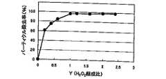
図4に、パーティクル除去率の薬液の過酸化水素組成比(Y)に対する依存性を示す。これは、シリコン基板上に設けられた酸化膜、SiGe膜(Si70原子%、Ge30原子%)および多結晶シリコン膜からなる積層膜をドライエッチングによりパターニングした後、その基板を、液温35℃、30質量%アンモニア水:30質量%過酸化水素水:水=1:Y:50(容量比)の組成の薬液を用いて1分間スピン方式で洗浄し、この処理前後のパーティクル数を測定して求めたものである。
【0047】
図4から、パーティクル除去率は用いる第2の薬液の過酸化水素組成比(Y)に依存し、特定の比率に至るまでは過酸化水素組成比(Y)が大きいほどパーティクル除去率が高くなる傾向があることがわかる。また、パーティクル除去率は、SiGe膜中のGe含有量にはほとんど依存しないことも確認された。すなわち、十分にパーティクルを除去するためには、薬液中のアンモニアに対する過酸化水素の含有比率が重要であり、特に上記条件においては過酸化水素組成比(Y)を1以上とすることにより、95%以上の高いパーティクル除去率を得ることができる。
【0048】
上述のとおり、第2の薬液(アンモニア水と過酸化水素水の混合液)を用いて基板を洗浄する第2の洗浄工程において、SiGe層のサイドエッチを抑制するためには薬液のアンモニア濃度が重要である。薬液のアンモニア濃度を低くするほど、特に特定の濃度以下にすることによりSiGe層のエッチレートを抑えることができ、サイドエッチを抑制することができる。一方、十分なパーティクル除去率を得るためには、薬液中のアンモニアに対する過酸化水素の含有比率が重要である。薬液中のアンモニアに対する過酸化水素の含有比率が特定の比率に至るまでは大きくなるほどパーティクル除去率が高くなる傾向がある。すなわち、第2の薬液の調製に際して、アンモニア水、過酸化水素水および水の混合比率を調整することにより、特に上記範囲内に設定することにより、SiGe層のサイドエッチを十分に抑制しつつ、高いパーティクル除去率を得ることができる。
【0049】
第2の薬液は、その所望の効果を損なわない範囲内で必要により他の添加成分を含有していてもよい。
【0050】
第2の薬液の使用温度は、SiGe層のサイドエッチの抑制や温度制御等の点から45℃以下が好ましく、40℃以下がより好ましく、35℃以下が特に好ましい。また、第2の薬液の使用温度は、温度制御やエネルギーコスト等の点から室温にできるだけ近い範囲にあることが望ましく、例えば上記温度範囲を上限として5℃以上、あるいは10℃以上、さらには15℃以上に設定することができる。
【0051】
図5に、SiGe層のサイドエッチ量と第2の薬液の液温との関係を示す。これは、シリコン基板上に設けられた酸化膜、SiGe膜および多結晶シリコン膜からなる積層膜をドライエッチングによりパターニングした後、その基板を、30質量%アンモニア水:30質量%過酸化水素水:水=1:1:50(容量比)の組成の薬液を用いて1分間スピン方式で洗浄し、この処理によるSiGe層のサイドエッチ量をSEMによる断面観察で測定したものである。SiGe膜としては、Si70原子%、Ge30原子%の膜(実線)およびSi60原子%、Ge40原子%の膜(点線)を用いた。
【0052】
図5から、SiGe層のサイドエッチ量は用いる第2の薬液の温度に大きく依存し、特定の温度を超えると薬液の温度が高いほどSiGe層のサイドエッチ量が大きくなる傾向があることがわかる。また、同じ液温の薬液を用いた場合、SiGe層中のGe含有量が多いほどSiGe層のサイドエッチ量が大きくなる傾向があることがわかる。すなわち、SiGe層のサイドエッチを抑制するためには、薬液の温度を低くすることが重要である。特に用いる薬液の温度を35℃以下とすることにより、Ge含有量にかかわらず、SiGe層のサイドエッチをほぼ完全に防止できることがわかる。
【0053】
ドライエッチングによるパターニングを行いゲート電極パターン及びゲート酸化膜パターンを形成した後、従来の洗浄方法により比較的高い液温で比較的高濃度のアンモニア水と過酸化水素水の混合液を用いて半導体基板を洗浄しようとすると、SiGe層ほどではないが、ゲート酸化膜もある程度はサイドエッチされる。そのため、従来の洗浄方法では、このゲート酸化膜のサイドエッチ量を素子特性の低下が問題とならない許容範囲内、例えば1nm以下にとどまるように洗浄条件を制御していた。本発明では、アンモニア水と過酸化水素水の混合液からなる第2の薬液を従来用いられる薬液より低濃度にできるため、第2の洗浄工程における第2の薬液によるゲート酸化膜のサイドエッチを十分に抑制あるいは防止することができる。さらに、第2の洗浄工程においてゲート酸化膜のサイドエッチを十分に抑制あるいは防止することができるため、ゲート酸化膜サイドエッチ量の許容範囲を十分に確保することができ、その結果、第1の洗浄工程において、第1の薬液として酸化物にエッチング性を示すフッ化水素酸を用いても、その許容範囲内にゲート酸化膜のサイドエッチ量を抑えながらエッチング生成物を除去することができる。
【0054】
第2の薬液による処理時間(洗浄時間)は、SiGe層の組成、第2の薬液の濃度や組成、液温などに応じて適宜設定することができる。SiGe層のサイドエッチを抑制する点および処理効率の点から、パーティクルを十分に除去できる時間を超えて長時間にわたって基板の洗浄を行わないことが好ましい。
【0055】
以上に説明した第2の洗浄工程の一例として、例えば、30質量%アンモニア水:30質量%過酸化水素水:水=1:1:50(容量比)の組成の第2の薬液を用い、スピン方式により液温35℃、処理時間30秒〜2分程度で洗浄を行うことができる。
【0056】
第2の洗浄工程の後には、必要により純水リンス工程を行うことができる。
【0057】
上記のようにしてアンモニア水と過酸化水素水の混合液からなる第2の薬液を用いて基板を洗浄した後に、必要により純水リンスした後には、スピン乾燥法などの公知の方法で基板を乾燥させることができる。
【0058】
以上のように、本実施形態では、ドライエッチングによるパターニングを行いSiGe層を含むゲート電極およびゲート酸化膜を形成した後、半導体基板を第3の薬液で処理してレジストを除去し、次にフッ化水素酸からなる第1の薬液を用いて半導体基板を洗浄し、最後にアンモニア水と過酸化水素水の混合液からなる第2の薬液を用いて半導体基板を洗浄する。これにより、SiGe層およびゲート酸化膜のサイドエッチを十分に抑制しつつ、半導体基板に付着したドライエッチ生成物およびパーティクルを十分に除去することができる。すなわち本発明によれば、パーティクル除去率90%以上、さらには95%以上で、且つSEM(走査型顕微鏡)で確認できないほどにドライエッチ生成物を除去することができ、このとき、ゲート電極のSiGe層のサイドエッチ量を1nm以下、さらには0.5nm以下にすることができるとともに、ゲート酸化膜のサイドエッチ量を1nm以下、さらには0.5nm以下にすることができる。
【0059】
本実施形態ではゲート電極パターン及びゲート酸化膜パターン形成後、第1の洗浄工程前に基板を第3の薬液で処理してレジストパターンを除去しているが、第1の洗浄工程後、第2の洗浄工程前にレジストパターンを除去してもよい。パーティクル除去の点からは、ゲート電極パターン及びゲート酸化膜パターン形成後、第1の洗浄工程前にレジストパターンを除去することが好ましい。
【0060】
また本発明では、パターニング工程(ゲート電極パターンおよびゲート酸化膜パターンの形成工程)から第2の洗浄工程までの間において、半導体基板を液体で処理した後に半導体基板を乾燥させる工程を含まないことが好ましい。薬液処理(洗浄、レジストの除去)や純水リンスなどの後に半導体基板を乾燥させる工程を行わず、半導体基板表面を常に濡れた状態に保つことで、半導体基板へのパーティクルの固着が抑制され、洗浄において容易にパーティクルを除去することができる。ここで「半導体基板を乾燥させる工程」とは、スピン乾燥法など、基板を乾燥させるための処理を行うことをいい、薬液処理工程から次の薬液処理工程までの自然乾燥は含まれない。ただし、薬液処理工程から次の薬液処理工程までの時間が短時間であるほど好ましい。
【0061】
この点から、スプレー方式で洗浄等を行う場合は、薬液処理工程から次の薬液処理工程に移行する際に洗浄装置から基板を取り出さず、用いる薬液を速やかに切り替えることが好ましい。また、ディップ方式で洗浄等の薬液処理を行う場合は、半導体基板を薬液処理槽から次の薬液処理槽へ移送する間に半導体基板に付着した薬液が乾燥しないように時間や温度を管理すること、または、半導体基板を薬液処理槽内の薬液から引き上げたりせずに槽内の薬液を漸次置換することが好ましい。
【0062】
次に、本発明において好適に用いられる洗浄装置の一実施形態について説明する。
【0063】
本発明で好適に用いられるスプレー方式の洗浄装置は、その一例として、処理チャンバー内に半導体基板を配置するための支持体と、配置された半導体基板を回転させる手段とを有し、処理チャンバー内にスプレーノズルが設置され、このスプレーノズルから液体が回転する半導体基板に吐出される構成を有している。このスプレーノズルは、最終的に半導体基板の乾燥時に導入される不活性ガスが吐出されるようになっていてもよい。また、このスプレーノズルは、吐出物(薬液や純水、不活性ガス等)ごとに別々に設けてもよいし、1つのノズルで2種以上を吐出するようにしてもよい。1つのノズルで2種以上を吐出するには、スプレーノズルに接続された供給ラインに切り替えバルブを設け、ある薬液または純水等を吐出した後、バルブを切り替えて次の薬液または純水等を吐出するようにすればよい。このような洗浄装置を用いることにより、用いる薬液や純水の切り替えを速やかに行うことができる。スプレーノズルから吐出され、基板に吹き付けられた薬液や純水は、排液として排液口から処理チャンバー外へ排出される。
【0064】
また、洗浄装置は、半導体基板を一枚ずつ処理する枚葉式の装置を用いてもよいし、処理チャンバー内に、複数の半導体基板が所定の間隔で載置されるキャリアを一又は二以上保持し、このキャリアを回転させる回転手段を有し、このキャリアの周囲に一以上のスプレーノズルが設置された構成を有するスプレー方式の洗浄装置を用いてもよい。
【0065】
また、スピン方式以外の装置として、例えば、複数の基板を所定の間隔で収納する収納容器と、この収納容器上に設けられた、好ましくは収納容器に対して相対的に移動可能な複数のスプレーノズルとを有する洗浄装置を用いることができる。
【0066】
本発明で好適に用いられるディップ方式の洗浄装置は、フッ化水素酸を貯めた第1の薬液処理槽と、第1の純水リンス槽と、アンモニア水と過酸化水素水の混合液を貯めた第2の薬液処理槽と、第2の純水リンス槽とがこの順に連続して設けられている装置を挙げることができる。さらに、第1の薬液処理槽の前段に、あるいは、第1の純水リンス槽と第2の薬液処理槽との間に、レジストを除去するための硫酸と過酸化水素水の混合液を貯めた第3の薬液処理槽と、それに続く第3の純水リンス槽とが設けられていてもよい。また、基板を搭載したキャリアを各処理槽に自動搬送する機構を備えていてもよい。また、薬液処理槽内でキャリアを揺り動かしたり、回転させたりする手段を有していてもよく、薬液に窒素ガス等をバブリングする手段を有していてもよい。さらに、第2の純水リンス槽の後段には、半導体基板を乾燥させるための乾燥処理部を設けてもよい。
【0067】
【発明の効果】
以上のように、本発明によれば、Si及びGeを含有するSiGe膜と酸化膜とを有する積層膜をドライエッチングによりパターニングしてゲート電極パターン及びゲート酸化膜パターンを形成した後、ゲートを構成するSiGe層とゲート酸化膜とを損傷させることなく、半導体基板に付着したドライエッチ生成物およびパーティクルを十分に除去することができ、素子特性および信頼性に優れた半導体装置を歩留りよく製造することができる。
【図面の簡単な説明】
【図1】本発明の半導体装置の製造方法を説明するための図である。
【図2】従来の半導体基板の洗浄方法の問題を説明するための図である。
【図3】SiGe膜のエッチレートと第2の薬液のアンモニア組成比(X)との関係を示すグラフである。
【図4】パーティクル除去率の第2の薬液の過酸化水素組成比(Y)に対する依存性を示すグラフである。
【図5】SiGe層のサイドエッチ量と第2の薬液の液温との関係を示すグラフである。
【符号の説明】
1 半導体基板
2 ゲート酸化膜
3 SiGe層
4 多結晶シリコン層
5 素子分離領域
11 シリコン基板
12 シリコン酸化膜
13 SiGe膜
14 導電性材料膜
15 素子分離領域
16 レジストパターン
22 ゲート酸化膜
23 SiGe層
24 導電性材料層[0001]
TECHNICAL FIELD OF THE INVENTION
The present invention relates to a method for manufacturing a semiconductor device having a gate electrode including a SiGe layer.
[0002]
[Prior art]
In the manufacture of a semiconductor device, a conductive film or an insulating film is patterned by forming a resist film on a conductive film or an insulating film formed on a semiconductor substrate and then forming a resist pattern by photolithography, or2 This is performed by forming a hard mask pattern made of a material such as the above, and etching the conductive film or the insulating film using these patterns as a mask. At this time, dry etching is usually performed to form a fine pattern. However, when patterning is performed by dry etching, foreign substances such as dry etch products and particles adhere to the semiconductor substrate. If the process proceeds to the next step in a state where such foreign matter is adhered, a reduction in the yield in manufacturing and a reduction in element characteristics and reliability are caused. Therefore, after patterning, it is necessary to clean the semiconductor substrate to sufficiently remove foreign substances attached to the substrate.
[0003]
The cleaning performed after the patterning of the insulating film is disclosed, for example, in Japanese Patent Application Laid-Open No. 4-142741, which relates to a semiconductor manufacturing apparatus for performing a chemical treatment on a semiconductor wafer. In this publication, a silicon oxide film on a silicon semiconductor wafer is wet-etched and patterned using a hydrofluoric acid-based processing solution (a mixed solution of hydrofluoric acid and ammonium fluoride), and then is etched with sulfuric acid and hydrogen peroxide solution. The substrate is treated with a mixture of the above to remove the photoresist, and then the wafer is washed with a mixture of aqueous ammonia, hydrogen peroxide and pure water to remove particles attached to the wafer surface. Has been described. The publication also states that particles are strongly adhered to the wafer surface due to the drying of the wafer, making it difficult to remove the particles. After the wet etching of the silicon oxide film, the photoresist and the particles are removed continuously. Describes that such a problem can be solved. Further, the publication discloses that the silicon oxide film etching apparatus can be applied to a polysilicon film etching apparatus.
[0004]
On the other hand, cleaning performed after patterning of the conductive film is disclosed in, for example, JP-A-2000-223364. This publication discloses that a gate electrode is formed by patterning a laminated film of a high melting point metal film (WSi film) and a polycrystalline silicon film on a semiconductor substrate by dry etching, and then forming an ammonia solution at a liquid temperature of 35 ° C. or 45 ° C. It describes that a substrate is cleaned using a mixed solution of hydrogen peroxide solution and an etching residue deposited on the substrate is removed.
[0005]
In Japanese Patent Application Laid-Open No. 2000-223364, when a substrate is washed for a long time using a mixed solution of ammonia and hydrogen peroxide, dissolution of the side surface of the WSi film constituting the gate electrode progresses, and a reduced film portion occurs. It is described. In the same publication, in order to substantially completely remove deposits such as dry etching residues while preventing such a decrease in the WSi film, the cleaning of the substrate is performed with a specific processing time determined using a dummy substrate. It has been proposed to do so. Also, in the same publication, a connection hole is formed by dry etching in an interlayer insulation film composed of a plurality of insulation films (silicon oxide film, BPSG film, BSG film) having different etching rates for wet processing, and the connection hole is formed on the surface of the connection hole. It is described that the etched etching residue is cleaned using a mixed solution of ammonia-hydrogen peroxide solution. Also in this cleaning, if the processing time is too long, unevenness is formed on the inner wall of the connection hole due to a difference in etching rate, so that the dummy substrate is removed for the purpose of removing the etching residue while preventing the occurrence of the unevenness. It describes that the washing is performed at a specific processing time determined using the washing.
[0006]
[Problems to be solved by the invention]
In recent years, a semiconductor device having a gate electrode including a SiGe layer and a polycrystalline silicon layer has been proposed from the viewpoint of improving the electrical characteristics of the element. For example, Y. V. Ponomarev et al. , IEDM '97, p. 829 includes a SiGe layer (poly-Si layer) in which the lower layer controls the work function.0.8 Ge0.2 ), A semiconductor device having a gate electrode of a polycrystalline silicon layer (poly-Si) as an upper layer has been proposed, and its element characteristics are also described in detail.
[0007]
Also, Wen-Chin Lee et al. , 1998 Symposium on VLSI Technology Digest of Technical Papers, p. Reference numeral 190 denotes a SiGe layer (poly-Si1-x Gex ) Is described. Ja-Hum Ku et al. , 2000 Symposium on VLSI Technology Digest of Technical Papers, p. Reference numeral 114 denotes a SiGe layer (poly-Si0.8 Ge0.2 ) Is deposited on the substrate and annealed to form a gate electrode (Ni (Six Ge1-x ) / Poly-Si0.8 Ge0.2 ) Is described.
[0008]
A gate pattern composed of a SiGe layer and a polycrystalline silicon layer is obtained by laminating an oxide film, a SiGe film, and a polycrystalline silicon film on a semiconductor substrate in this order, forming a resist film on the laminated film, and then forming a resist film by photolithography. A pattern is formed, and the laminated film is formed by dry etching using the resist pattern as a mask. However, after patterning by dry etching as described above to form a gate electrode pattern and a gate oxide film pattern composed of a SiGe layer and a polycrystalline silicon layer, the gate electrode pattern and the gate oxide film pattern were formed by a chemical reaction between an etching gas and an object to be etched. Dry etch products and particles adhere to the surface of the semiconductor substrate and the gate electrode. Therefore, it is necessary to clean the semiconductor substrate to remove these deposits.
[0009]
However, when cleaning is performed by a conventional cleaning method using a mixed solution of ammonia water and hydrogen peroxide water to remove dry etch products and particles attached to the semiconductor substrate and the gate electrode, the side surface of the SiGe layer is removed. There is a problem that the film is reduced (hereinafter referred to as "side etch" as appropriate).
[0010]
The above problem of the conventional cleaning method will be further described with reference to FIG. FIG. 2A is a schematic sectional view of the semiconductor substrate after the formation of the gate electrode pattern and the gate oxide film pattern before the cleaning, and FIG. 2B is a schematic sectional view of the semiconductor substrate after the cleaning. In the figure,
[0011]
As described above, when the laminated film including the SiGe film is dry-etched using the resist pattern as a mask (FIG. 2A), dry-etch products and particles (not shown) adhere to the surface of the semiconductor substrate and the gate electrode. In order to remove dry etch products and particles attached to the semiconductor substrate in this manner, a mixed solution of ammonia water and hydrogen peroxide solution used in a conventional cleaning method can be used. In order to sufficiently remove substances, it is necessary to increase the ammonia concentration and the liquid temperature. This is presumably because the dry etch product derived from the SiGe layer is difficult to dissolve in this mixture.
[0012]
However, if cleaning is performed using a mixed solution having a high ammonia concentration at a high temperature so that the dry etch product can be sufficiently removed, the
[0013]
That is, in the conventional cleaning method using a mixed solution of ammonia water and hydrogen peroxide solution as a chemical solution (cleaning liquid) used for cleaning, dry etch products or particles adhered to the semiconductor substrate are prevented while preventing side etching of the SiGe layer. Was very difficult to remove. In addition, in order to obtain good device characteristics, it is necessary not to damage the gate oxide film.
[0014]
Therefore, an object of the present invention is to form a gate electrode pattern and a gate oxide film pattern by patterning a laminated film having a SiGe film containing Si and Ge and an oxide film by dry etching, and then forming an SiGe layer constituting a gate. It is an object of the present invention to sufficiently remove dry etch products and particles attached to a semiconductor substrate without damaging a gate oxide film and manufacture a semiconductor device having excellent element characteristics and reliability with a high yield.
[0015]
[Means for Solving the Problems]
According to the present invention, there is provided a method for manufacturing a semiconductor device having a gate oxide film on a semiconductor substrate and a gate electrode including a SiGe layer containing Si and Ge,
A patterning step of forming a gate electrode pattern and an oxide film pattern by dry etching a laminated film in which an oxide film and a SiGe film containing Si and Ge are formed in this order on a semiconductor substrate;
After the patterning step, using a first chemical solution of hydrofluoric acid, a first cleaning step of cleaning the semiconductor substrate on which the laminated film has been patterned;
A method of manufacturing a semiconductor device, comprising: after the first cleaning step, a second cleaning step of cleaning the semiconductor substrate using a second chemical solution composed of a mixed solution of ammonia water and hydrogen peroxide solution. You.
[0016]
According to the present invention, the ammonia concentration of the second chemical solution is 0.05 to 1.5% by mass,
There is provided a method for manufacturing a semiconductor device, wherein a content ratio (by mass) of hydrogen peroxide to ammonia in the second chemical solution is 1 or more (hydrogen peroxide / ammonia).
[0017]
Further, according to the present invention, there is provided a method of manufacturing a semiconductor device, wherein the use temperature of the second chemical solution is 45 ° C. or less in the second cleaning step.
[0018]
Further, according to the present invention, there is provided a method of manufacturing a semiconductor device, wherein the first chemical solution has a hydrogen fluoride concentration of 0.05 to 1.0% by mass.
[0019]
In the present invention, a gate electrode pattern and a gate oxide film pattern are formed by patterning a laminated film having an oxide film and a SiGe film in this order by dry etching, and then etching products and particles attached to the semiconductor substrate are removed. Cleaning is performed in two stages. That is, two-stage cleaning is performed: a first cleaning process suitable for removing etching products, and a second cleaning process suitable for removing particles. This makes it possible to use a chemical solution optimal for the object to be removed in each cleaning step, and to obtain an excellent cleaning effect. Furthermore, since the cleaning effect of the chemical solution on the object to be removed is high, and the concentration, composition, and cleaning conditions of the chemical solution can be set for each cleaning step, the SiGe layer and the gate can be sufficiently secured while the cleaning effect on the object to be removed is sufficiently ensured. The solubility of the chemical solution in the oxide film, that is, the side etch of the SiGe layer and the gate oxide film can be sufficiently suppressed.
[0020]
The first cleaning step in the present invention is for cleaning a semiconductor substrate using a first chemical solution composed of hydrofluoric acid, mainly for the purpose of removing dry etch products. The present inventor has found that hydrofluoric acid used as the first chemical solution has a very low particle-removing power, but a very high dry-etching product removing power. It is generally known that hydrofluoric acid has a high oxide removing ability, and if it is used as a cleaning solution in a state where the gate oxide film is exposed, the gate oxide film is easily damaged. However, since hydrofluoric acid has a very high ability to remove dry etch products, it has been found that dry etch products can be sufficiently removed even when the concentration of oxides is reduced to lower the concentration. That is, in the present invention, by using hydrofluoric acid as the first chemical solution, it is possible to sufficiently remove the dry etch product while sufficiently suppressing the side etch of the gate oxide film. Further, the etch rate of the first chemical solution made of hydrofluoric acid with respect to the SiGe layer is low, and there is no problem of side etching of the SiGe layer in the first cleaning step.
[0021]
The second cleaning step in the present invention is mainly for removing particles, and cleans the semiconductor substrate using a second chemical solution composed of a mixed solution of aqueous ammonia and aqueous hydrogen peroxide. The inventor of the present invention has reported that the mixed solution of ammonia water and hydrogen peroxide used as the second chemical solution does not have high removal power of dry etch products, but has very low particle removal power in a specific composition range. I found it expensive. A mixed solution of ammonia water and hydrogen peroxide solution is generally known as a cleaning liquid. However, the etching rate of the SiGe layer is extremely high at a conventional concentration, and particles can be sufficiently removed when used in the second cleaning step. Then, side etching of the SiGe layer occurs. However, as long as the content ratio of ammonia and hydrogen peroxide is controlled to a specific range, the present inventor is required in the present invention even if the etch rate of the SiGe layer is lowered by lowering the concentration of the chemical solution. It has been found that sufficient particle removing power can be obtained. That is, in the present invention, particles can be sufficiently removed while sufficiently suppressing side etching of the SiGe layer by using a mixed solution of ammonia water and hydrogen peroxide solution as the second chemical solution. In addition, the etch rate of the second chemical solution composed of a mixed solution of ammonia water and hydrogen peroxide solution with respect to the gate oxide film is low, and there is no problem of side etching of the gate oxide film in the second cleaning step.
[0022]
As described above, according to the present invention, a gate electrode pattern and a gate oxide film pattern are formed by patterning a laminated film having an oxide film and a SiGe film in this order on a semiconductor substrate by dry etching, and then mainly performing dry etching. By cleaning the semiconductor substrate in a first cleaning step for removing an object and a second cleaning step for mainly removing particles, side etching of the SiGe layer of the gate electrode and the gate oxide film is performed. , And dry etch products and particles attached to the semiconductor substrate can be sufficiently removed. As a result, a semiconductor device having excellent element characteristics and reliability can be manufactured with high yield.
[0023]
BEST MODE FOR CARRYING OUT THE INVENTION
Hereinafter, preferred embodiments of the present invention will be described.
[0024]
A method for manufacturing a semiconductor device having a gate electrode including a SiGe layer according to the present invention will be described with reference to FIG.
[0025]
First, a
[0026]
Next, a
[0027]
Next, a
[0028]
Further, in the present invention, the gate electrode can be constituted only by the SiGe layer into which the n-type impurity or the p-type impurity is introduced. In this case, the next step, that is, formation of the resist
[0029]
Next, after a photoresist is applied on the
[0030]
Then, using the resist
[0031]
After forming a gate electrode and a gate oxide film by patterning by dry etching as described above, the substrate is treated with a third chemical solution to remove the resist
[0032]
After the semiconductor substrate is treated with the third chemical solution to remove the resist
[0033]
Next, the substrate is cleaned using a first chemical solution composed of hydrofluoric acid for the purpose of mainly removing dry etch products (first cleaning step). This cleaning can be performed by a spray method or a dip method. The spray method is a method of cleaning by spraying a chemical solution on the substrate while preferably rotating the substrate, and the dipping method is a method of immersing the substrate in a tank (chemical solution processing tank) storing the chemical solution and washing the substrate. is there.
[0034]
The hydrogen fluoride concentration of the first chemical solution is preferably 0.05% by mass or more, more preferably 0.1% by mass or more, and particularly preferably 0.13% by mass or more. Further, the hydrogen fluoride concentration of the first chemical solution is preferably 1.0% by mass or less, more preferably 0.9% by mass or less, further preferably 0.8% by mass or less, and particularly preferably 0.7% by mass or less. . When the concentration of the first chemical solution is high, the ability to remove dry etch products increases, but when the concentration of the chemical solution is too high, the etch rate of the gate oxide film increases, and the etch rate becomes so large that side etching becomes a problem. On the other hand, if the concentration of the chemical solution is too high, it is necessary to shorten the cleaning time in order to prevent side etching, so that the dry etching product tends to remain, and the cleaning operation becomes difficult in controlling the cleaning time. Conversely, when the concentration of the chemical solution is low, the etch rate of the gate oxide film becomes small, and the side etch of the gate oxide film can be suppressed, but the ability to remove dry etch products becomes small. Therefore, by setting the composition of the first chemical solution within the above range, the dry etch product attached to the semiconductor substrate can be more sufficiently removed while the side etch of the gate oxide film is more sufficiently suppressed. .
[0035]
The first chemical solution may contain other additive components as needed as long as the desired effect is not impaired.
[0036]
The use temperature of the first chemical is preferably 40 ° C. or lower, more preferably 35 ° C. or lower, and particularly preferably 30 ° C. or lower. By setting the use temperature of the first chemical solution within the above range, the side etching of the gate oxide film can be more sufficiently suppressed. Further, the use temperature of the first chemical solution is preferably 5 ° C or higher, more preferably 10 ° C or higher, and particularly preferably 15 ° C or higher. By setting the use temperature of the first chemical solution within the above range, the dry etch product attached to the substrate can be more sufficiently removed.
[0037]
The processing time (cleaning time) with the first chemical solution can be appropriately set according to the concentration and composition of the first chemical solution, the liquid temperature, the amount and type of the dry etch product attached to the substrate, the cleaning method, and the like. . From the viewpoint of suppressing the side etching of the gate oxide film and the processing efficiency, it is preferable not to perform the cleaning of the substrate for a long time beyond the time that the dry etching product can be sufficiently removed.
[0038]
As an example of the first cleaning step described above, for example, a first chemical solution composed of 0.17% by mass of hydrofluoric acid is used, and the cleaning is performed by a spin method at a liquid temperature of 20 ° C. and a processing time of about 3 to 6 minutes. It can be performed.
[0039]
After the first cleaning step, a pure water rinsing step can be performed if necessary.
[0040]
After cleaning the semiconductor substrate using the first chemical solution composed of hydrofluoric acid as described above, rinsing with pure water after the cleaning if necessary, and then removing ammonia particles mainly for the purpose of removing particles. The semiconductor substrate is cleaned using a second chemical solution composed of a mixed solution of hydrogen peroxide water (second cleaning step). This cleaning can be performed by a spray method or a dip method.
[0041]
The ammonia concentration of the second chemical solution is preferably 0.05% by mass or more, more preferably 0.1% by mass or more, and particularly preferably 0.2% by mass or more. Further, the ammonia concentration of the second chemical solution is preferably 1.5% by mass or less, more preferably 1.4% by mass or less, still more preferably 1.3% by mass or less, and particularly preferably 1.2% by mass or less.
[0042]
The content ratio of hydrogen peroxide to ammonia in the second chemical solution (hydrogen peroxide / ammonia; on a mass basis) is preferably 1 or more, more preferably 1.1 or more, and particularly preferably 1.2 or more. Further, the content ratio of hydrogen peroxide to ammonia (hydrogen peroxide / ammonia; mass basis) in the second chemical solution is preferably 5 or less, more preferably 3 or less, and particularly preferably 2 or less.
[0043]
The etch rate of the SiGe layer tends to decrease as the ammonia concentration in the second chemical solution decreases, but the particle removal power tends to decrease if the ammonia concentration is too low. On the other hand, as the content ratio of hydrogen peroxide to ammonia in the second chemical solution increases up to a specific ratio, there is a tendency that the particle removing power of the chemical solution increases. Further, it is not preferable in terms of cost to make the content ratio of hydrogen peroxide to ammonia in the chemical solution too large. In view of the above, by setting the composition of the second chemical solution to the above range, particles attached to the semiconductor substrate can be more sufficiently removed while side etching of the SiGe layer is more sufficiently suppressed.
[0044]
FIG. 3 shows the relationship between the etch rate of the SiGe film and the ammonia composition ratio (X) of the second chemical solution. That is, a substrate provided with a SiGe film is immersed in a chemical solution having a composition of liquid temperature 35 ° C., 30 mass% ammonia water: 30 mass% hydrogen peroxide solution: water = X: 1: 50 (volume ratio) for a predetermined time. And the thickness of the SiGe film before and after the treatment. As the SiGe film, a film of 70 atomic% of Si and 30 atomic% of Ge (solid line) and a film of 60 atomic% of Si and 40 atomic% of Ge (dotted line) were used.
[0045]
From FIG. 3, the etch rate of the SiGe film greatly depends on the ammonia composition ratio (X) of the second chemical used, that is, the ammonia concentration. When the ammonia concentration exceeds a specific ammonia concentration, the etch rate of the SiGe film increases as the ammonia concentration increases. It turns out that there is a tendency. In addition, when chemical solutions having the same composition are used, it can be seen that the higher the Ge content in the SiGe layer, the higher the etch rate of the SiGe layer. That is, in order to reduce the etch rate of the SiGe film and suppress the side etch of the SiGe film, it is important to lower the ammonia concentration of the chemical solution. In particular, it can be seen that by setting the ammonia composition ratio X of the chemical solution to 1 or less, etching of the SiGe layer can be almost completely prevented regardless of the Ge content.
[0046]
FIG. 4 shows the dependency of the particle removal rate on the hydrogen peroxide composition ratio (Y) of the chemical solution. This is because a laminated film composed of an oxide film, a SiGe film (70 atomic% of Si, 30 atomic% of Ge) and a polycrystalline silicon film provided on a silicon substrate is patterned by dry etching, and then the substrate is heated at a liquid temperature of 35 ° C. 30% by mass ammonia water: 30% by mass hydrogen peroxide solution: water = 1: Washed by a spin method for 1 minute using a chemical solution having a composition of 50 (volume ratio), and the number of particles before and after this treatment was measured. It is what I sought.
[0047]
From FIG. 4, the particle removal rate depends on the hydrogen peroxide composition ratio (Y) of the second chemical used, and the particle removal rate increases as the hydrogen peroxide composition ratio (Y) increases up to a specific ratio. It can be seen that there is a tendency. It was also confirmed that the particle removal rate hardly depends on the Ge content in the SiGe film. That is, in order to sufficiently remove particles, the content ratio of hydrogen peroxide to ammonia in the chemical solution is important. In particular, under the above conditions, by setting the hydrogen peroxide composition ratio (Y) to 1 or more, 95 % Or more can be obtained.
[0048]
As described above, in the second cleaning step of cleaning the substrate using the second chemical solution (a mixed solution of ammonia water and hydrogen peroxide solution), in order to suppress the side etch of the SiGe layer, the ammonia concentration of the chemical solution is reduced. is important. As the ammonia concentration of the chemical solution is lowered, the etch rate of the SiGe layer can be suppressed and the side etch can be suppressed particularly by setting the ammonia concentration to a specific concentration or less. On the other hand, in order to obtain a sufficient particle removal rate, the content ratio of hydrogen peroxide to ammonia in the chemical is important. The particle removal rate tends to increase as the content ratio of hydrogen peroxide to ammonia in the chemical solution increases up to a specific ratio. That is, when preparing the second chemical solution, by adjusting the mixing ratio of ammonia water, hydrogen peroxide solution and water, particularly by setting the mixing ratio within the above range, while sufficiently suppressing the side etch of the SiGe layer, A high particle removal rate can be obtained.
[0049]
The second chemical solution may contain other additive components as needed as long as the desired effect is not impaired.
[0050]
The use temperature of the second chemical solution is preferably 45 ° C. or less, more preferably 40 ° C. or less, and particularly preferably 35 ° C. or less from the viewpoint of suppressing the side etch of the SiGe layer and controlling the temperature. Further, the use temperature of the second chemical solution is desirably in a range as close as possible to room temperature from the viewpoint of temperature control and energy cost, for example, 5 ° C. or higher, 10 ° C. or higher, and even 15 ° C or higher.
[0051]
FIG. 5 shows a relationship between the side etch amount of the SiGe layer and the temperature of the second chemical solution. This is because, after a laminated film composed of an oxide film, a SiGe film, and a polycrystalline silicon film provided on a silicon substrate is patterned by dry etching, the substrate is subjected to 30% by mass ammonia water: 30% by mass hydrogen peroxide solution: Washing was performed by a spin method for 1 minute using a chemical solution having a composition of water = 1: 1: 50 (volume ratio), and the side etch amount of the SiGe layer by this treatment was measured by cross-sectional observation using an SEM. As the SiGe film, a film of 70 atomic% of Si and 30 atomic% of Ge (solid line) and a film of 60 atomic% of Si and 40 atomic% of Ge (dotted line) were used.
[0052]
From FIG. 5, it can be seen that the side etch amount of the SiGe layer largely depends on the temperature of the second chemical used, and when the temperature exceeds a specific temperature, the side etch amount of the SiGe layer tends to increase as the temperature of the chemical increases. . In addition, when chemical solutions having the same liquid temperature are used, it is found that the side etch amount of the SiGe layer tends to increase as the Ge content in the SiGe layer increases. That is, in order to suppress side etching of the SiGe layer, it is important to lower the temperature of the chemical solution. In particular, it can be seen that by setting the temperature of the used chemical solution to 35 ° C. or less, side etching of the SiGe layer can be almost completely prevented regardless of the Ge content.
[0053]
After patterning by dry etching to form a gate electrode pattern and a gate oxide film pattern, a semiconductor substrate is formed by a conventional cleaning method using a mixed solution of ammonia water and hydrogen peroxide at a relatively high liquid temperature and a relatively high concentration. Is to be cleaned, the gate oxide film is side-etched to some extent, though not as much as the SiGe layer. For this reason, in the conventional cleaning method, the cleaning conditions are controlled so that the side etch amount of the gate oxide film is kept within an allowable range where deterioration of device characteristics does not cause a problem, for example, 1 nm or less. In the present invention, since the second chemical solution composed of a mixed solution of ammonia water and hydrogen peroxide solution can be made lower in concentration than the conventionally used chemical solution, the side etching of the gate oxide film by the second chemical solution in the second cleaning step is reduced. It can be sufficiently suppressed or prevented. Further, since the side etching of the gate oxide film can be sufficiently suppressed or prevented in the second cleaning step, the allowable range of the amount of side etching of the gate oxide film can be sufficiently ensured. In the cleaning step, even if hydrofluoric acid having an etching property for oxide is used as the first chemical solution, the etching product can be removed while suppressing the side etch amount of the gate oxide film within the allowable range.
[0054]
The processing time (cleaning time) with the second chemical solution can be appropriately set according to the composition of the SiGe layer, the concentration and composition of the second chemical solution, the liquid temperature, and the like. From the viewpoint of suppressing the side etching of the SiGe layer and the processing efficiency, it is preferable that the substrate is not cleaned for a long time beyond the time when the particles can be sufficiently removed.
[0055]
As an example of the second cleaning step described above, for example, a second chemical solution having a composition of 30% by mass ammonia water: 30% by mass hydrogen peroxide solution: water = 1: 1: 50 (volume ratio) is used. Cleaning can be performed by a spin method with a liquid temperature of 35 ° C. and a processing time of about 30 seconds to 2 minutes.
[0056]
After the second cleaning step, a pure water rinsing step can be performed if necessary.
[0057]
After washing the substrate with the second chemical solution composed of a mixture of aqueous ammonia and hydrogen peroxide as described above, and after rinsing with pure water as necessary, the substrate is removed by a known method such as spin drying. Can be dried.
[0058]
As described above, in the present embodiment, after patterning by dry etching to form the gate electrode and the gate oxide film including the SiGe layer, the semiconductor substrate is treated with the third chemical solution to remove the resist, and then the fluorine is removed. The semiconductor substrate is cleaned using a first chemical solution made of hydrofluoric acid, and finally, the semiconductor substrate is cleaned using a second chemical solution made of a mixed solution of aqueous ammonia and hydrogen peroxide. This makes it possible to sufficiently remove dry etch products and particles attached to the semiconductor substrate while sufficiently suppressing the side etch of the SiGe layer and the gate oxide film. That is, according to the present invention, the dry etch product can be removed at a particle removal rate of 90% or more, more preferably 95% or more and so as not to be confirmed by an SEM (scanning microscope). The side etch amount of the SiGe layer can be set to 1 nm or less, and further, 0.5 nm or less, and the side etch amount of the gate oxide film can be set to 1 nm or less, and further, 0.5 nm or less.
[0059]
In this embodiment, after forming the gate electrode pattern and the gate oxide film pattern and before the first cleaning step, the substrate is treated with a third chemical solution to remove the resist pattern. The resist pattern may be removed before the washing step. From the viewpoint of particle removal, it is preferable to remove the resist pattern after forming the gate electrode pattern and the gate oxide film pattern and before the first cleaning step.
[0060]
Further, in the present invention, between the patterning step (the step of forming the gate electrode pattern and the gate oxide film pattern) and the second cleaning step, a step of drying the semiconductor substrate after treating the semiconductor substrate with a liquid may not be included. preferable. The semiconductor substrate surface is always kept wet without performing a process of drying the semiconductor substrate after chemical treatment (washing, resist removal), pure water rinsing, etc., thereby suppressing the adhesion of particles to the semiconductor substrate, Particles can be easily removed during cleaning. Here, the “step of drying the semiconductor substrate” refers to performing a process for drying the substrate, such as a spin drying method, and does not include natural drying from the chemical solution processing step to the next chemical solution processing step. However, the shorter the time from the chemical treatment step to the next chemical treatment step, the better.
[0061]
From this point, when cleaning or the like is performed by a spray method, it is preferable that the chemical solution to be used be quickly changed without taking out the substrate from the cleaning device when the chemical solution processing step is shifted to the next chemical solution processing step. When performing chemical treatment such as cleaning in the dipping method, control the time and temperature so that the chemical attached to the semiconductor substrate does not dry while the semiconductor substrate is transferred from the chemical treatment tank to the next chemical treatment tank. Alternatively, it is preferable that the chemical liquid in the tank is gradually replaced without pulling up the semiconductor substrate from the chemical liquid in the chemical processing tank.
[0062]
Next, an embodiment of a cleaning apparatus suitably used in the present invention will be described.
[0063]
The spray-type cleaning apparatus preferably used in the present invention includes, as an example, a support for arranging a semiconductor substrate in a processing chamber, and means for rotating the arranged semiconductor substrate. The spray nozzle is installed in the nozzle, and the liquid is discharged from the spray nozzle to the rotating semiconductor substrate. The spray nozzle may discharge an inert gas that is finally introduced when the semiconductor substrate is dried. Further, this spray nozzle may be provided separately for each discharge substance (chemical liquid, pure water, inert gas, etc.), or one nozzle may discharge two or more types. In order to discharge two or more types with one nozzle, a switching valve is provided in the supply line connected to the spray nozzle, and after discharging a certain chemical solution or pure water, the valve is switched to supply the next chemical solution or pure water. What is necessary is just to make it discharge. By using such a cleaning device, the chemical solution or pure water to be used can be quickly switched. The chemical solution or pure water discharged from the spray nozzle and sprayed on the substrate is discharged from the discharge port to the outside of the processing chamber as drainage.
[0064]
In addition, the cleaning apparatus may use a single-wafer type apparatus that processes semiconductor substrates one by one, or a carrier in which a plurality of semiconductor substrates are placed at predetermined intervals in a processing chamber. It is also possible to use a spray-type cleaning apparatus having a rotating means for holding and rotating the carrier, and having a configuration in which one or more spray nozzles are installed around the carrier.
[0065]
In addition, as a device other than the spin method, for example, a storage container that stores a plurality of substrates at predetermined intervals, and a plurality of sprays provided on the storage container, preferably movable relatively to the storage container. A cleaning device having a nozzle can be used.
[0066]
The dip-type cleaning apparatus preferably used in the present invention stores a first chemical treatment tank storing hydrofluoric acid, a first pure water rinsing tank, and a mixed liquid of ammonia water and hydrogen peroxide water. An apparatus in which a second chemical treatment tank and a second pure water rinsing tank are successively provided in this order. Further, a mixed solution of sulfuric acid and hydrogen peroxide for removing the resist is stored before the first chemical liquid processing tank or between the first pure water rinsing tank and the second chemical liquid processing tank. A third chemical solution treatment tank and a third pure water rinsing tank following the third chemical treatment tank may be provided. Further, a mechanism for automatically transporting a carrier on which a substrate is mounted to each processing tank may be provided. Further, a means for rocking or rotating the carrier in the chemical solution treatment tank may be provided, and a means for bubbling nitrogen gas or the like into the chemical solution may be provided. Further, a drying section for drying the semiconductor substrate may be provided downstream of the second pure water rinsing tank.
[0067]
【The invention's effect】
As described above, according to the present invention, after forming a gate electrode pattern and a gate oxide film pattern by patterning a laminated film having a SiGe film containing Si and Ge and an oxide film by dry etching, a gate is formed. To sufficiently remove dry etch products and particles attached to a semiconductor substrate without damaging the resulting SiGe layer and gate oxide film, and to manufacture a semiconductor device having excellent device characteristics and reliability with high yield. Can be.
[Brief description of the drawings]
FIG. 1 is a view illustrating a method for manufacturing a semiconductor device according to the present invention.
FIG. 2 is a view for explaining a problem of a conventional semiconductor substrate cleaning method.
FIG. 3 is a graph showing a relationship between an etch rate of a SiGe film and an ammonia composition ratio (X) of a second chemical solution.
FIG. 4 is a graph showing the dependence of a particle removal rate on a hydrogen peroxide composition ratio (Y) of a second chemical solution.
FIG. 5 is a graph showing a relationship between a side etch amount of a SiGe layer and a liquid temperature of a second chemical solution.
[Explanation of symbols]
1 semiconductor substrate
2 Gate oxide film
3 SiGe layer
4 Polycrystalline silicon layer
5 Device isolation area
11 Silicon substrate
12 Silicon oxide film
13 SiGe film
14 Conductive material film
15 Device isolation area
16 Resist pattern
22 Gate oxide film
23 SiGe layer
24 conductive material layer
Claims (6)
Translated fromJapanese半導体基板上に、酸化膜と、Si及びGeを含有するSiGe膜とがこの順で形成された積層膜をドライエッチングしてゲート電極パターンおよび酸化膜パターンを形成するパターニング工程と、
前記パターニング工程の後、フッ化水素酸からなる第1の薬液を用いて、前記積層膜がパターニングされた半導体基板を洗浄する第1の洗浄工程と、
前記第1の洗浄工程の後、アンモニア水と過酸化水素水の混合液からなる第2の薬液を用いて前記半導体基板を洗浄する第2の洗浄工程と
を有する半導体装置の製造方法。A method of manufacturing a semiconductor device having a gate oxide film and a gate electrode including a SiGe layer containing Si and Ge on a semiconductor substrate,
A patterning step of forming a gate electrode pattern and an oxide film pattern by dry etching a laminated film in which an oxide film and a SiGe film containing Si and Ge are formed in this order on a semiconductor substrate;
After the patterning step, using a first chemical solution of hydrofluoric acid, a first cleaning step of cleaning the semiconductor substrate on which the laminated film has been patterned;
After the first cleaning step, a second cleaning step of cleaning the semiconductor substrate using a second chemical solution composed of a mixed solution of ammonia water and hydrogen peroxide solution.
前記第2の薬液中のアンモニアに対する過酸化水素の含有比率(質量基準)が1以上(過酸化水素/アンモニア)である請求項1に記載の半導体装置の製造方法。The second chemical solution has an ammonia concentration of 0.05 to 1.5% by mass;
2. The method of manufacturing a semiconductor device according to claim 1, wherein a content ratio (by mass) of hydrogen peroxide to ammonia in the second chemical solution is 1 or more (hydrogen peroxide / ammonia). 3.
Priority Applications (2)
| Application Number | Priority Date | Filing Date | Title |
|---|---|---|---|
| JP2003112438AJP2004006819A (en) | 2002-04-26 | 2003-04-17 | Method for manufacturing semiconductor device |
| US10/422,302US6790734B2 (en) | 2002-04-26 | 2003-04-24 | Manufacturing method of semiconductor device |
Applications Claiming Priority (2)
| Application Number | Priority Date | Filing Date | Title |
|---|---|---|---|
| JP2002125827 | 2002-04-26 | ||
| JP2003112438AJP2004006819A (en) | 2002-04-26 | 2003-04-17 | Method for manufacturing semiconductor device |
Publications (1)
| Publication Number | Publication Date |
|---|---|
| JP2004006819Atrue JP2004006819A (en) | 2004-01-08 |
Family
ID=29714275
Family Applications (1)
| Application Number | Title | Priority Date | Filing Date |
|---|---|---|---|
| JP2003112438APendingJP2004006819A (en) | 2002-04-26 | 2003-04-17 | Method for manufacturing semiconductor device |
Country Status (2)
| Country | Link |
|---|---|
| US (1) | US6790734B2 (en) |
| JP (1) | JP2004006819A (en) |
Cited By (2)
| Publication number | Priority date | Publication date | Assignee | Title |
|---|---|---|---|---|
| KR100811267B1 (en) | 2005-12-22 | 2008-03-07 | 주식회사 하이닉스반도체 | Method of fabricating the dual gate in semiconductor device |
| WO2015072552A1 (en)* | 2013-11-18 | 2015-05-21 | 富士フイルム株式会社 | Semiconductor substrate treatment liquid, treatment method, and manufacturing method of semiconductor substrate product using these |
Families Citing this family (8)
| Publication number | Priority date | Publication date | Assignee | Title |
|---|---|---|---|---|
| US7320931B2 (en)* | 2004-07-30 | 2008-01-22 | Freescale Semiconductor Inc. | Interfacial layer for use with high k dielectric materials |
| US7176090B2 (en)* | 2004-09-07 | 2007-02-13 | Intel Corporation | Method for making a semiconductor device that includes a metal gate electrode |
| US20070154637A1 (en)* | 2005-12-19 | 2007-07-05 | Rohm And Haas Electronic Materials Llc | Organometallic composition |
| KR20090080786A (en)* | 2008-01-22 | 2009-07-27 | 삼성전자주식회사 | Manufacturing Method of Array Substrate and Array Substrate |
| US7943527B2 (en)* | 2008-05-30 | 2011-05-17 | The Board Of Trustees Of The University Of Illinois | Surface preparation for thin film growth by enhanced nucleation |
| US8258587B2 (en)* | 2008-10-06 | 2012-09-04 | Taiwan Semiconductor Manufacturing Company, Ltd. | Transistor performance with metal gate |
| KR20150088941A (en)* | 2014-01-24 | 2015-08-04 | 삼성전자주식회사 | Wet station and method of using the same |
| US10767143B2 (en)* | 2014-03-06 | 2020-09-08 | Sage Electrochromics, Inc. | Particle removal from electrochromic films using non-aqueous fluids |
Family Cites Families (14)
| Publication number | Priority date | Publication date | Assignee | Title |
|---|---|---|---|---|
| US4300581A (en) | 1980-03-06 | 1981-11-17 | Thompson Raymon F | Centrifugal wafer processor |
| JPS58114042A (en) | 1981-12-28 | 1983-07-07 | Ricoh Co Ltd | Color - Color reproduction adjustment method in electrophotography |
| JP3158407B2 (en) | 1990-01-17 | 2001-04-23 | ソニー株式会社 | Semiconductor substrate cleaning method |
| JPH04142741A (en) | 1990-10-04 | 1992-05-15 | Nec Corp | Semiconductor manufacturing device |
| JP2888217B2 (en) | 1996-12-12 | 1999-05-10 | 日本電気株式会社 | Method for controlling concentration of cleaning chemical solution and silicon wafer cleaning apparatus |
| DE19840989A1 (en)* | 1997-09-09 | 1999-03-18 | Tokyo Electron Ltd | Object wet cleaning method for e.g. semiconductor wafer |
| US5989948A (en)* | 1997-09-22 | 1999-11-23 | Vlsi Technology, Inc. | Methods of forming pairs of transistors, and methods of forming pairs of transistors having different voltage tolerances |
| JP3109471B2 (en)* | 1998-03-31 | 2000-11-13 | 日本電気株式会社 | Cleaning / drying equipment and semiconductor device manufacturing line |
| JP2000188292A (en)* | 1998-12-21 | 2000-07-04 | Mitsubishi Electric Corp | Semiconductor device and manufacturing method |
| JP2000223464A (en) | 1999-02-02 | 2000-08-11 | Nec Corp | Board cleaning method |
| US6664196B1 (en)* | 1999-03-15 | 2003-12-16 | Matsushita Electric Industrial Co., Ltd. | Method of cleaning electronic device and method of fabricating the same |
| US6410436B2 (en)* | 1999-03-26 | 2002-06-25 | Canon Kabushiki Kaisha | Method of cleaning porous body, and process for producing porous body, non-porous film or bonded substrate |
| US6613695B2 (en)* | 2000-11-24 | 2003-09-02 | Asm America, Inc. | Surface preparation prior to deposition |
| TWI220060B (en)* | 2001-05-10 | 2004-08-01 | Macronix Int Co Ltd | Cleaning method of semiconductor wafer |
- 2003
- 2003-04-17JPJP2003112438Apatent/JP2004006819A/enactivePending
- 2003-04-24USUS10/422,302patent/US6790734B2/ennot_activeExpired - Fee Related
Cited By (4)
| Publication number | Priority date | Publication date | Assignee | Title |
|---|---|---|---|---|
| KR100811267B1 (en) | 2005-12-22 | 2008-03-07 | 주식회사 하이닉스반도체 | Method of fabricating the dual gate in semiconductor device |
| WO2015072552A1 (en)* | 2013-11-18 | 2015-05-21 | 富士フイルム株式会社 | Semiconductor substrate treatment liquid, treatment method, and manufacturing method of semiconductor substrate product using these |
| JP2015099831A (en)* | 2013-11-18 | 2015-05-28 | 富士フイルム株式会社 | Processing liquid for semiconductor substrate, processing method, and method of manufacturing semiconductor substrate product using them |
| US10199210B2 (en) | 2013-11-18 | 2019-02-05 | Fujifilm Corporation | Semiconductor substrate treatment liquid, treatment method, and method for manufacturing semiconductor-substrate product using these |
Also Published As
| Publication number | Publication date |
|---|---|
| US20030228744A1 (en) | 2003-12-11 |
| US6790734B2 (en) | 2004-09-14 |
Similar Documents
| Publication | Publication Date | Title |
|---|---|---|
| CN100353488C (en) | Method for producing semiconductor device and cleaning device for resist stripping | |
| JP7343543B2 (en) | Removal methods for high aspect ratio structures | |
| US6890391B2 (en) | Method of manufacturing semiconductor device and apparatus for cleaning substrate | |
| JP2001237236A (en) | Cleaning method of substrate surfaces after etching process | |
| WO2004076605A1 (en) | Dilute sulfuric peroxide at point-of-use | |
| JP7258915B2 (en) | Method and apparatus used for cleaning semiconductor wafers | |
| KR100706798B1 (en) | Cleaning method of substrate exposed silicon film and silicon germanium film and semiconductor manufacturing method using same | |
| JP2009081247A (en) | Ruthenium film etching method | |
| CN102931073A (en) | Method for manufacturing semiconductor device | |
| JP2004006819A (en) | Method for manufacturing semiconductor device | |
| KR20020018022A (en) | Method of fabricating semiconductor device and wafer treatment apparatus employed therefor as well as semiconductor device | |
| US20100099258A1 (en) | Semiconductor device cleaning method and semiconductor device manufacturing method using the same | |
| JP2002231699A (en) | Cleaning method of silicon electrode for fluorocarbon- based plasma generation, and manufacturing method of semiconductor device | |
| JP3371149B2 (en) | Method for manufacturing semiconductor device | |
| KR100762907B1 (en) | Gate Forming Method of Semiconductor Device | |
| JP2008147434A (en) | Manufacturing method of semiconductor device | |
| US7267127B2 (en) | Method for manufacturing electronic device | |
| JP3401585B2 (en) | Substrate cleaning method | |
| CN101157569A (en) | A method for non-destructive etching of silicon carbide | |
| KR100900223B1 (en) | Manufacturing method of semiconductor device | |
| KR20080088246A (en) | Semiconductor substrate cleaning method | |
| JP2009135137A (en) | Cleaning method and cleaning device | |
| JP2006319151A (en) | Etching residue removing method and manufacturing method of semiconductor device using the same | |
| US20050092348A1 (en) | Method for cleaning an integrated circuit device using an aqueous cleaning composition | |
| KR100732860B1 (en) | Ashing method after oxide film etching on semiconductor substrate |
Legal Events
| Date | Code | Title | Description |
|---|---|---|---|
| A977 | Report on retrieval | Free format text:JAPANESE INTERMEDIATE CODE: A971007 Effective date:20040928 | |
| A131 | Notification of reasons for refusal | Free format text:JAPANESE INTERMEDIATE CODE: A131 Effective date:20041102 | |
| A521 | Written amendment | Free format text:JAPANESE INTERMEDIATE CODE: A523 Effective date:20041222 | |
| RD03 | Notification of appointment of power of attorney | Free format text:JAPANESE INTERMEDIATE CODE: A7423 Effective date:20041222 | |
| RD04 | Notification of resignation of power of attorney | Free format text:JAPANESE INTERMEDIATE CODE: A7424 Effective date:20041222 | |
| A02 | Decision of refusal | Free format text:JAPANESE INTERMEDIATE CODE: A02 Effective date:20050426 |