EP4222744B1 - Split-gate non-volatile memory cells with erase gates disposed over word line gates, and method of making same - Google Patents
Split-gate non-volatile memory cells with erase gates disposed over word line gates, and method of making sameDownload PDFInfo
- Publication number
- EP4222744B1 EP4222744B1EP21709281.6AEP21709281AEP4222744B1EP 4222744 B1EP4222744 B1EP 4222744B1EP 21709281 AEP21709281 AEP 21709281AEP 4222744 B1EP4222744 B1EP 4222744B1
- Authority
- EP
- European Patent Office
- Prior art keywords
- gate
- insulated
- floating gate
- word line
- erase
- Prior art date
- Legal status (The legal status is an assumption and is not a legal conclusion. Google has not performed a legal analysis and makes no representation as to the accuracy of the status listed.)
- Active
Links
Images


Classifications
- G—PHYSICS
- G11—INFORMATION STORAGE
- G11C—STATIC STORES
- G11C16/00—Erasable programmable read-only memories
- G11C16/02—Erasable programmable read-only memories electrically programmable
- G11C16/04—Erasable programmable read-only memories electrically programmable using variable threshold transistors, e.g. FAMOS
- G11C16/0408—Erasable programmable read-only memories electrically programmable using variable threshold transistors, e.g. FAMOS comprising cells containing floating gate transistors
- G11C16/0425—Erasable programmable read-only memories electrically programmable using variable threshold transistors, e.g. FAMOS comprising cells containing floating gate transistors comprising cells containing a merged floating gate and select transistor
- G—PHYSICS
- G11—INFORMATION STORAGE
- G11C—STATIC STORES
- G11C16/00—Erasable programmable read-only memories
- G11C16/02—Erasable programmable read-only memories electrically programmable
- G11C16/04—Erasable programmable read-only memories electrically programmable using variable threshold transistors, e.g. FAMOS
- G11C16/0408—Erasable programmable read-only memories electrically programmable using variable threshold transistors, e.g. FAMOS comprising cells containing floating gate transistors
- G11C16/0433—Erasable programmable read-only memories electrically programmable using variable threshold transistors, e.g. FAMOS comprising cells containing floating gate transistors comprising cells containing a single floating gate transistor and one or more separate select transistors
- H—ELECTRICITY
- H10—SEMICONDUCTOR DEVICES; ELECTRIC SOLID-STATE DEVICES NOT OTHERWISE PROVIDED FOR
- H10B—ELECTRONIC MEMORY DEVICES
- H10B41/00—Electrically erasable-and-programmable ROM [EEPROM] devices comprising floating gates
- H10B41/30—Electrically erasable-and-programmable ROM [EEPROM] devices comprising floating gates characterised by the memory core region
- H—ELECTRICITY
- H10—SEMICONDUCTOR DEVICES; ELECTRIC SOLID-STATE DEVICES NOT OTHERWISE PROVIDED FOR
- H10D—INORGANIC ELECTRIC SEMICONDUCTOR DEVICES
- H10D30/00—Field-effect transistors [FET]
- H10D30/01—Manufacture or treatment
- H10D30/021—Manufacture or treatment of FETs having insulated gates [IGFET]
- H10D30/0411—Manufacture or treatment of FETs having insulated gates [IGFET] of FETs having floating gates
- H—ELECTRICITY
- H10—SEMICONDUCTOR DEVICES; ELECTRIC SOLID-STATE DEVICES NOT OTHERWISE PROVIDED FOR
- H10D—INORGANIC ELECTRIC SEMICONDUCTOR DEVICES
- H10D30/00—Field-effect transistors [FET]
- H10D30/60—Insulated-gate field-effect transistors [IGFET]
- H10D30/68—Floating-gate IGFETs
- H—ELECTRICITY
- H10—SEMICONDUCTOR DEVICES; ELECTRIC SOLID-STATE DEVICES NOT OTHERWISE PROVIDED FOR
- H10D—INORGANIC ELECTRIC SEMICONDUCTOR DEVICES
- H10D30/00—Field-effect transistors [FET]
- H10D30/60—Insulated-gate field-effect transistors [IGFET]
- H10D30/68—Floating-gate IGFETs
- H10D30/6891—Floating-gate IGFETs characterised by the shapes, relative sizes or dispositions of the floating gate electrode
- H10D30/6892—Floating-gate IGFETs characterised by the shapes, relative sizes or dispositions of the floating gate electrode having at least one additional gate other than the floating gate and the control gate, e.g. program gate, erase gate or select gate
- G—PHYSICS
- G11—INFORMATION STORAGE
- G11C—STATIC STORES
- G11C2216/00—Indexing scheme relating to G11C16/00 and subgroups, for features not directly covered by these groups
- G11C2216/02—Structural aspects of erasable programmable read-only memories
- G11C2216/04—Nonvolatile memory cell provided with a separate control gate for erasing the cells, i.e. erase gate, independent of the normal read control gate
Definitions
- the present inventionrelates to non-volatile memory arrays, and more particularly to a split gate, memory cell design and method of manufacture.
- split gate non-volatile memory cellsand arrays of such cells, are well known.
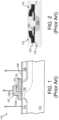
- U.S. Patent 5,029,130(“the '130 patent”) discloses an array of split gate non-volatile memory cells.
- the memory cellis shown in Fig. 1 .
- Each memory cell 110includes source and drain regions 114/116 formed in a semiconductor substrate 112, with a channel region 118 there between.
- a floating gate 120is formed over and insulated from (and controls the conductivity of) a first portion of the channel region 118, and over a portion of the drain region 116.
- a control gate 122has a first portion 122a that is disposed over and insulated from (and controls the conductivity of) a second portion of the channel region 118, and a second portion 122b that extends up and over the floating gate 120.
- the floating gate 120 and control gate 122are insulated from the substrate 112 by a gate oxide 126.
- the memory cellis erased (where electrons are removed from the floating gate) by placing a high positive voltage on the control gate 122, which causes electrons on the floating gate 120 to tunnel through the intermediate insulation 123 from the floating gate 120 to the control gate 122 via Fowler-Nordheim tunneling.
- the memory cellis programmed (where electrons are placed on the floating gate) by placing a positive voltage on the control gate 122, and a positive voltage on the drain region 116. Electron current will flow from the source region 114 towards the drain region 116. The electrons will accelerate and become heated when they reach the gap between the control gate 122 and the floating gate 120. Some of the heated electrons will be injected through the gate oxide 126 onto the floating gate 120 due to the attractive electrostatic force from the floating gate 120.
- the memory cellis read by placing positive read voltages on the drain region 116 and control gate 122 (which turns on the channel region 118 under the control gate first portion 122a). If the floating gate 120 is positively charged (i.e. erased of electrons and positively coupled to the drain region 116), then the portion of the channel region 118 under the floating gate 120 is turned on as well, and current will flow across the channel region 118, which is sensed as the erased or "1" state. If the floating gate 120 is negatively charged (i.e. programmed with electrons), then the portion of the channel region under the floating gate 120 is mostly or entirely turned off, and current will not flow (or there will be little flow) across the channel region 118, which is sensed as the programmed or "0" state.
- the source and drain regionscan be interchangeable, where the floating gate 120 can extend partially over the source region 114 instead of the drain region 116, as shown in Fig. 2 .
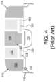
- a four gate memory disclosed in U.S. Patent 6,747,310(“the '310 patent”).
- the memory cellshave source region 114, drain region 116, floating gate 120 over a first portion of channel region 118, a select (word line) gate 128 over a second portion of the channel region 118, a control gate 122 over the floating gate 120, and an erase gate 130 over the source region 114.
- Programmingis shown by heated electrons from the channel region 118 injecting themselves onto the floating gate 120.
- Erasingis shown by electrons tunneling from the floating gate 120 to the erase gate 130 by placing a positive voltage on the erase gate 130 (and optionally a negative voltage on the control gate 122).
- this configurationis not ideal because erase efficiency can be compromised by the high coupling ratio between the erase gate and the floating gate, and it can be complex to manufacture.
- a non-volatile memory having memory cellsis provided.
- a stacked gate structurehas gate dielectric layer, assist gate, insulation layer, and erase gate disposed in order.
- the floating gateis disposed on a first sidewall of the stacked gate structure, the floating gate has a corner portion at the top portion, and erase gate covers the corner portion.
- the tunneling dielectric layeris disposed under the floating gate.
- the erase gate dielectric layeris disposed between the erase gate and the floating gate.
- the assist gate dielectric layeris disposed between the assist gate and the floating gate.
- the source region and the drain regionare respectively disposed at two sides of the stacked structure and the floating gate.
- the control gateis disposed on the source region and the floating gate.
- the inter-gate dielectric layeris disposed between the control gate and the floating gate.
- a memorycomprises: a substrate; a dielectric region formed on the substrate; a source-contacted layer formed in the dielectric region; a first source diffusion formed in the substrate; a first drain diffusion formed in the substrate; a first floating gate formed in the dielectric region; a first control gate formed in the dielectric region; a first erase gate formed in the dielectric region; and a first source diffusion via electrically coupling the first source diffusion to the source-contacted layer.
- a memory devicethat includes a substrate of semiconductor material of a first conductivity type, first and second regions spaced apart in the substrate and having a second conductivity type different than the first conductivity type, with a first channel region in the substrate extending between the first and second regions, a first floating gate disposed over and insulated from a first portion of the first channel region adjacent to the second region, a first coupling gate disposed over and insulated from the first floating gate, a first word line gate disposed over and insulated from a second portion of the first channel region adjacent the first region, and a first erase gate disposed over and insulated from the first word line gate.
- a method of forming memory cellsincludes forming a first insulation layer on a semiconductor substrate having a first conductivity type, forming a first conductive layer on the first insulation layer, forming a second insulation layer on the first conductive layer, forming a second conductive layer on the second insulation layer, forming a third insulation layer on the second conductive layer, forming a trench that extends through the third insulation layer, the second conductive layer, and the second insulation layer, forming insulation spacers along a sidewall of the trench, extending the trench through the first conductive layer between the insulation spacers, forming a first block of conductive material in the trench, wherein the first block of conductive material is disposed vertically over and insulated from the substrate and laterally adjacent to and insulated from the first conductive layer, forming first and second erase gates in the trench, wherein the first and second erase gates are disposed vertically over and insulated from the first block of conductive material, removing a portion of the first block of conductive material between the first and second erase gates, while maintaining first and
- the first floating gateis disposed over and insulated from the substrate and laterally adjacent to and insulated from the first word line gate.
- the second floating gateis disposed over and insulated from the substrate and laterally adjacent to and insulated from the second word line gate.
- the first coupling gateis disposed over and insulated from the first floating gate.
- the second coupling gateis disposed over and insulated from the second floating gate.
- the first erase gateis disposed over and insulated from the first word line gate.
- the second erase gateis disposed over and insulated from the second word line gate
- the present inventionis a memory cell design, architecture and method of manufacture of a split-gate, memory cell design.
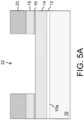
- FIGs 5A-5Fthere are shown cross-sectional views of the steps in the process to make a memory cell. While only the formation of a pair of memory cells is shown in the figures, it should be understood that an array of such memory cell pairs are formed concurrently when forming a memory device containing an array of such memory cells.
- the processbegins by forming a first insulation layer 12 (e.g. layer of silicon dioxide, also referred to herein as oxide layer 12) on the top surface 10a of a substrate 10 of semiconductor material (e.g., single crystalline silicon).
- a first conductive layer 14e.g.
- polysiliconalso referred to herein as "poly" or amorphous silicon
- a second insulation layer 16is formed on first conductive layer 14.
- second insulation layer 16is an ONO layer, meaning it has oxide-nitride-oxide sublayers.
- a second conductive layer 18e.g. polysilicon or amorphous silicon
- a third insulation layer 20e.g. silicon nitride - referred to herein as "nitride” is formed on second conductive layer 18.
- Photoresist material(not shown) is coated on the structure, and a photolithography masking step is performed exposing selected portions of the photoresist material.
- the photoresistis developed such that portions of the photoresist are removed. Using the remaining photoresist as a mask, the structure is etched. Specifically, third insulation layer 20, second conductive layer 18 and second insulation layer 16 are anisotropically etched (using conductive layer 14 as an etch stop), leaving a trench 22 extending through third insulation layer 20, second conductive layer 18 and second insulation layer 16. The resulting structure is shown in Fig. 5A (after photoresist removal).
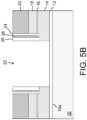
- Insulation spacers 24/26(e.g., ON - oxide and nitride, respectively) spacers 24/26 are formed along the sidewalls of trench 22. Formation of spacers is well known in the art, and involves the deposition of a material over the contour of a structure, followed by an anisotropic etch process, whereby the material is removed from horizontal surfaces of the structure, while the material remains largely intact on vertically oriented surfaces of the structure (with a rounded upper surface, not shown). Insulation (ON) spacers 24/26 are formed by oxide deposition, nitride deposition, and then nitride anisotropic etch and oxide anisotropic etch.
- Oxide spacers 28are then formed in trench 22 by oxide deposition followed by oxide anisotropic etch. An anisotropic etch is then performed to remove the exposed portion of first conductive layer 14 below the area located between oxide spacers 28, as shown in Fig. 5B , deepening trench 22. An implantation may be performed at this time (through oxide layer 12 at the bottom of trench 22 and into the portion of the substrate 10 underneath (which will eventually be the word line portion of the channel region as described further below).
- Oxide spacers 30are next formed along the sidewalls of trench 22 (including along the exposed sidewalls of first conductive layer 14 and adjacent oxide spacers 28) by oxide deposition and anisotropic oxide etch. This spacer formation, particularly the anisotropic oxide etch which removes the portion of oxide layer 12 at the bottom of trench 22, leaves the portion of the substrate surface 10a between oxide spacers 30 exposed. Oxide layer 32 is formed on this exposed portion of the substrate surface 10a at the bottom of trench 22, preferably by thermal oxidation. Also preferably oxide layer 32 has a thickness that is less than that of oxide layer 12.
- a first block of conductive material 34is formed on oxide layer 32 inside trench 22 by material deposition, a chemical mechanical polish (CMP) using third insulation layer 20 as a stop layer, and etch back.
- the first block of conductive material 34is formed of polysilicon, and the top surface of the first block of conductive material 34 is below the top surface of the first conductive layer 14.
- the first block of conductive material 34is laterally adjacent to, and insulated from, first conductive layer 14 by oxide spacers 30.
- An implantationcan be performed to dope the first block of conductive material 34 should polysilicon be used for the first block of conductive material 34.
- the resulting structureis shown in Fig. 5C .
- An oxide etch(e.g., wet etch) is used to remove the upper portions of oxide spacers 30 (above the first block of conductive material 34) and all of oxide spacers 28.
- An oxide layer 36is then formed over the structure by oxide deposition.
- Second and third blocks of conductive material 38a/38bare formed on oxide layer 36 inside trench 22 by material deposition and etch.
- second and third blocks of conductive material 38a/38bare a pair of spaced apart spacers formed by polysilicon deposition and anisotropic etch, leaving the portion of oxide layer 36 between the second and third blocks of conductive material 38a/38b exposed
- An oxide etchis used to remove the exposed portion of oxide layer 36 at the bottom of the trench 22 between the second and third blocks of conductive material (e.g., by anisotropic etch), leaving a portion of the first block of conductive material 34 exposed.
- An etchis then used to remove the exposed (middle) portion of the first block of conductive material 34, resulting in fourth and fifth blocks of conductive material 34a/34b remaining from the first block of conductive material 34.
- the resulting structureis shown in Fig. 5D .
- Drain region 40is a first region in the substrate 10 having a conductivity type different from that of the substrate 10 in the vicinity of the drain region 40.
- Photoresist material 42is coated on the structure, and a photolithography masking step is performed exposing selected portions of the photoresist material. The photoresist material 42 is developed such that portions of the photoresist material 42 are removed (except for photoresist material 42 in trench 22, over the second and third blocks of conductive material 38a/38b, over layer 36, over spacers 24/26, and over portions of third insulation layer 20 adjacent the second and third blocks of conductive material 38a/38b).
- first and second source regions 44a and 44bare second and third regions in the substrate that have the same conductivity type as that of drain region 40 (i.e., different from that of the substrate 10 in the vicinity of the first and second source regions 44a/44b), and extend partially under the respective adjacent first conductive layer 14.
- first and second source regions 44a/44b and drain region 40can be P type conductivity, and the first and second source regions 44a/44b and drain region 40 can be N type conductivity, and vice-versa.
- insulation spacers 48e.g., nitride
- a pair of memory cellsi.e. memory cells 50 and 52, are formed sharing a common drain region 40.
- a first channel region 46ais defined in the substrate 10 by, and extends between, first source region 44a and the drain region 40.
- a first floating gate 14a(a first block of material remaining from first conductive layer 14) is disposed over and insulated from a first portion of the first channel region 46a (for controlling the conductivity thereof) adjacent first source region 44a, and preferably the first floating gate 14a is partially disposed over and insulated from first source region 44a by a respective remaining portion of oxide layer 12.
- a first coupling gate 18a(a first block of material remaining from second conductive layer 18) is disposed over and insulated from the first floating gate 14a by a respective remaining portion of second insulation layer 16 (for voltage coupling to the floating gate 14a).
- the fourth block of conductive material 34ais a first word line gate that is disposed vertically over and insulated from a second portion of the first channel region 46a (for controlling the conductivity thereof), and is laterally adjacent to and insulated from the first floating gate 14a by a respective remaining portion of oxide spacer 30.
- the second block of conductive material 38ais a first erase gate that is disposed vertically over and insulated from the first word line gate 34a by a respective remaining portion of oxide layer 36, and laterally adjacent to and insulated from the first coupling gate 18a by a combination of respective remaining portions of oxide layer 36 and insulation spacers 24, 26.
- the first erase gate 38aincludes a notch 38c facing an edge 14c of the first floating gate 14a.
- Insulation block 20a(block of material remaining from insulation layer 20) is disposed over first coupling gate 18a.
- a second channel region 46bis defined in the substrate 10 by, and extends between, source region 44b and the drain region 40.
- a second floating gate 14b(a second block of material remaining from first conductive layer 14) is disposed over and insulated from a first portion of the second channel region 46b (for controlling the conductivity thereof) adjacent source region 44b, and preferably the second floating gate 14b is partially disposed over and insulated from second source region 44b by a respective remaining portion of oxide layer 12.
- a second coupling gate 18b(a second block of material remaining from second conductive layer 18) is disposed over and insulated from the second floating gate 14b by a respective remaining portion of second insulation layer 16 (for voltage coupling to the floating gate 14b).
- the fifth block of conductive material 34bis a second word line gate that is disposed vertically over and insulated from a second portion of the second channel region 46b (for controlling the conductivity thereof), and is laterally adjacent to and insulated from the second floating gate 14b by a respective remaining portion of oxide spacer 30.
- the third block of conductive material 38bis a second erase gate that is disposed vertically over and insulated from the second word line gate 34b by a respective remaining portion of oxide layer 36, and laterally adjacent to and insulated from the second coupling gate 18b by a combination of respective remaining portions of oxide layer 36 and insulation spacers 24, 26.
- the second erase gate 38bincludes a notch 38c facing an edge 14c of the second floating gate 14b. Insulation block 20b (block of material remaining from insulation layer 20) is disposed over second coupling gate 18b
- Table 1illustrates exemplary operational voltages and currents for program, read and erase operations of the memory cells 50 and 52.
- Table 1EG 38a EG 38b WLG 34a WLG 34b CG 18a CG 18b Source 44a Source 44b Drain 40
- Program Cell 504.5V 0V 1.0V 0V 10.5 V 0V 4.5V 0V -1uA
- Program Cell 520V 4.5V 0V 1.0V 0V 10.5 V 0V 4.5V -1uA
- Read Cell 500V 0V Vcc 0V Vcc 0V 0V 0V 0V Vblr Read Cell 52 0V 0V 0V Vcc 0V Vcc 0V 0V Vblr
- Erase Cell 5011.5V 0V 0V 0V 0V 0V 0V 0V 0V 0V 0V 0V V 0V Vcc can be, for
- Programming memory cell 50(i.e., programming first floating gate 14a with electrons) stores a first bit of information
- programming memory cell 52i.e., programming second floating gate 14b with electrons
- a positive voltage of 4.5 Vis applied to first erase gate 38a
- a positive voltage of 1 Vis applied to first word line gate 34a
- a positive voltage of 10.5 Vis applied to first coupling gate 18a
- a positive voltage of 4.5 Vis applied to first source region 44a
- a current of -1uAis applied to the drain region 40.
- Electronstravel from drain region 40 toward first source region 44a in first channel region 46a, and inject themselves onto first floating gate 14a because of the positive voltage capacitively coupled to first floating gate 14a by first coupling gate 18a.
- Memory cell 52is similarly programmed using the combination of voltages and current in Table 1.
- a positive voltage of 11.5 Vis applied to the first erase gate 38a, which causes electrons to tunnel through the insulation layer 36 from the first floating gate 14a to the first erase gate 38a.
- Memory cell 52is similarly erased by applying a positive voltage of 11.5 V to second erase gate 38b. Notches 38a facing edges 14c enhance the efficiency of this tunneling.
- Vcce.g., 0.9-3.3 V
- Vblre.g., 0.5-1.1 V
- Currentwill flow through the first channel region 46a if memory cell 50 is erased (i.e., first floating gate 14a is in an erased state and thus will have a positive voltage due to positive charge on first floating gate 14a after erasing and small voltage coupling from word line gate 34a and therefore the portion of the first channel region 46a under first floating gate 14a is turned on).
- the formation and resulting structure of memory cells 50 and 52have many advantages.
- the insulation (i.e., oxide layer 32) under the first and second word line gates 34a/34bcan be much thinner than the insulation (i.e., oxide layer 12) under the first and second floating gates 14a/14b, for higher performance especially for high speed applications.
- the insulation (i.e., oxide layer 36) between the first and second floating gates 14a/14b and the first and second erase gates 38a/38bcan be thinner than the insulation (i.e., oxide spacer 30) between the first and second floating gates 14a/14b and the first and second word line gates 34a/34b.
- the erase performanceis enhanced because of the relatively low voltage coupling ratio between the first and second erase gates 38a/38b and the first and second floating gates 14a/14b (because only the corner regions of first and second erase gates 38a/38b (with notches 38c) are in close proximity to the corner regions (with edges 14c) of the first and second floating gates 14a/14b). Only two photolithography masking steps are needed to define the structure, one for forming trench 22, and one for etching through conductive layers 18 and 14 to complete the formation of first and second coupling gates 18a/18b and first and second floating gates 14a/14b. Both word line gates 34a/38b and first and second erase gates 38a/38b are self-aligned to the first and second floating gates 14a/14b.
- This self-alignmentprovide better control over the lengths of the first and second channel regions 46a/46b.
- the ability to scale the memory cells 50/52 to smaller sizesis facilitated by having the first and second coupling gates 18a/18b disposed over the first and second floating gates 14a/14b respectively, and having the first and second erase gates 38a/38b disposed over the first and second word line gates 34a/34b respectively.
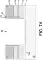
- Figs. 7A-7Billustrate an alternate embodiment for forming the memory cells 50/52, which starts with the structure of Fig. 5A .
- the above processing steps described with respect to Fig. 5Bare performed, except the formation of oxide spacers 28 is omitted, resulting in the structure shown in Fig. 7A .
- the remaining processing steps described above with respect to Figs. 5C-5Fare performed (except that the oxide spacers 28 are not removed because they were never formed), resulting in the final structure shown in Fig. 7B .
- the primary difference between this final structure and that of Fig. 6is that notches are not formed in the erase gate.
- nitride spacers 26are aligned with the sides of first and second floating gates 14a/14b, which means the sidewalls of trench 22 are planar when first and second erase gates 38a/38b are formed. Even though the lack of notches in the first and second erase gates 38a/38b may reduce erase efficiency, the memory cells 50/52 may be scaled down in size more than if the notches are formed and the lack of notches will reduce capacitive coupling between the first and second erase gates 38a/38b and the first and second floating gates 14a/14b.
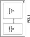
- Control circuitry 96preferably (but not necessarily) formed on the same substrate 10 (as shown in Fig. 8 ) is configured to program, read and erase an array 98 of the memory cells 50 or 52 described herein by applying the voltages of Table 1 as described above.
- the term “adjacent”includes “directly adjacent” (no intermediate materials, elements or space disposed there between) and “indirectly adjacent” (intermediate materials, elements or space disposed there between), “mounted to” includes “directly mounted to” (no intermediate materials, elements or space disposed there between) and “indirectly mounted to” (intermediate materials, elements or spaced disposed there between), and “electrically coupled” includes “directly electrically coupled to” (no intermediate materials or elements there between that electrically connect the elements together) and “indirectly electrically coupled to” (intermediate materials or elements there between that electrically connect the elements together).
- forming an element "over a substrate”can include forming the element directly on the substrate with no intermediate materials/elements there between, as well as forming the element indirectly on the substrate with one or more intermediate materials/elements there between.
Landscapes
- Engineering & Computer Science (AREA)
- Microelectronics & Electronic Packaging (AREA)
- Non-Volatile Memory (AREA)
- Semiconductor Memories (AREA)
Description
- This patent application claims priority to
Chinese Patent Application No. 202011060967.0, filed on September 30, 2020 U.S. Patent Application No. 17/165,934, filed on February 2, 2021 - The present invention relates to non-volatile memory arrays, and more particularly to a split gate, memory cell design and method of manufacture.
- Split gate non-volatile memory cells, and arrays of such cells, are well known. For example,
U.S. Patent 5,029,130 ("the '130 patent") discloses an array of split gate non-volatile memory cells. The memory cell is shown inFig. 1 . Eachmemory cell 110 includes source anddrain regions 114/116 formed in asemiconductor substrate 112, with achannel region 118 there between. Afloating gate 120 is formed over and insulated from (and controls the conductivity of) a first portion of thechannel region 118, and over a portion of thedrain region 116. Acontrol gate 122 has afirst portion 122a that is disposed over and insulated from (and controls the conductivity of) a second portion of thechannel region 118, and asecond portion 122b that extends up and over thefloating gate 120. Thefloating gate 120 andcontrol gate 122 are insulated from thesubstrate 112 by agate oxide 126. - The memory cell is erased (where electrons are removed from the floating gate) by placing a high positive voltage on the
control gate 122, which causes electrons on thefloating gate 120 to tunnel through theintermediate insulation 123 from thefloating gate 120 to thecontrol gate 122 via Fowler-Nordheim tunneling. - The memory cell is programmed (where electrons are placed on the floating gate) by placing a positive voltage on the
control gate 122, and a positive voltage on thedrain region 116. Electron current will flow from thesource region 114 towards thedrain region 116. The electrons will accelerate and become heated when they reach the gap between thecontrol gate 122 and thefloating gate 120. Some of the heated electrons will be injected through thegate oxide 126 onto thefloating gate 120 due to the attractive electrostatic force from thefloating gate 120. - The memory cell is read by placing positive read voltages on the
drain region 116 and control gate 122 (which turns on thechannel region 118 under the control gatefirst portion 122a). If thefloating gate 120 is positively charged (i.e. erased of electrons and positively coupled to the drain region 116), then the portion of thechannel region 118 under thefloating gate 120 is turned on as well, and current will flow across thechannel region 118, which is sensed as the erased or "1" state. If thefloating gate 120 is negatively charged (i.e. programmed with electrons), then the portion of the channel region under thefloating gate 120 is mostly or entirely turned off, and current will not flow (or there will be little flow) across thechannel region 118, which is sensed as the programmed or "0" state. Those skilled in the art understand that the source and drain regions can be interchangeable, where thefloating gate 120 can extend partially over thesource region 114 instead of thedrain region 116, as shown inFig. 2 . - Split gate memory cells having more than two gates are also known. For example,
U.S. Patent 8,711,636 ("the '636 patent") discloses memory cells with an additional coupling gate disposed over and insulated from the source region, for better capacitive coupling to the floating gate. See for exampleFig. 3 showingcoupling gate 124 disposed oversource region 114. - A four gate memory disclosed in
U.S. Patent 6,747,310 ("the '310 patent"). For example, as shown inFig. 4 , the memory cells havesource region 114,drain region 116, floatinggate 120 over a first portion ofchannel region 118, a select (word line)gate 128 over a second portion of thechannel region 118, acontrol gate 122 over thefloating gate 120, and an erase gate 130 over thesource region 114. Programming is shown by heated electrons from thechannel region 118 injecting themselves onto thefloating gate 120. Erasing is shown by electrons tunneling from thefloating gate 120 to the erase gate 130 by placing a positive voltage on the erase gate 130 (and optionally a negative voltage on the control gate 122). However, this configuration is not ideal because erase efficiency can be compromised by the high coupling ratio between the erase gate and the floating gate, and it can be complex to manufacture. - Conventional memory cell designs and methods of fabrication make it challenging to scale the memory cells down in size while maintaining or even enhancing performance, and streamlining fabrication processes.
US 20170040334 A1 discloses that a non-volatile memory having memory cells is provided. A stacked gate structure has gate dielectric layer, assist gate, insulation layer, and erase gate disposed in order. The floating gate is disposed on a first sidewall of the stacked gate structure, the floating gate has a corner portion at the top portion, and erase gate covers the corner portion. The tunneling dielectric layer is disposed under the floating gate. The erase gate dielectric layer is disposed between the erase gate and the floating gate. The assist gate dielectric layer is disposed between the assist gate and the floating gate. The source region and the drain region are respectively disposed at two sides of the stacked structure and the floating gate. The control gate is disposed on the source region and the floating gate. The inter-gate dielectric layer is disposed between the control gate and the floating gate.US 20190206882 A1 discloses that a memory comprises: a substrate; a dielectric region formed on the substrate; a source-contacted layer formed in the dielectric region; a first source diffusion formed in the substrate; a first drain diffusion formed in the substrate; a first floating gate formed in the dielectric region; a first control gate formed in the dielectric region; a first erase gate formed in the dielectric region; and a first source diffusion via electrically coupling the first source diffusion to the source-contacted layer.- The present invention is defined in the independent claims. Preferred embodiments are defined in the dependent claims.
- The aforementioned problems and needs are addressed by a memory device that includes a substrate of semiconductor material of a first conductivity type, first and second regions spaced apart in the substrate and having a second conductivity type different than the first conductivity type, with a first channel region in the substrate extending between the first and second regions, a first floating gate disposed over and insulated from a first portion of the first channel region adjacent to the second region, a first coupling gate disposed over and insulated from the first floating gate, a first word line gate disposed over and insulated from a second portion of the first channel region adjacent the first region, and a first erase gate disposed over and insulated from the first word line gate.
- A method of forming memory cells includes forming a first insulation layer on a semiconductor substrate having a first conductivity type, forming a first conductive layer on the first insulation layer, forming a second insulation layer on the first conductive layer, forming a second conductive layer on the second insulation layer, forming a third insulation layer on the second conductive layer, forming a trench that extends through the third insulation layer, the second conductive layer, and the second insulation layer, forming insulation spacers along a sidewall of the trench, extending the trench through the first conductive layer between the insulation spacers, forming a first block of conductive material in the trench, wherein the first block of conductive material is disposed vertically over and insulated from the substrate and laterally adjacent to and insulated from the first conductive layer, forming first and second erase gates in the trench, wherein the first and second erase gates are disposed vertically over and insulated from the first block of conductive material, removing a portion of the first block of conductive material between the first and second erase gates, while maintaining first and second portions of the first block of conductive material as respective first and second word line gates, forming a first region in a portion of the substrate between the first and second word line gates and having a second conductivity type different than the first conductivity type, removing portions of the second conductive layer while maintaining first and second portions of the second conductive layer as respective first and second coupling gates, removing portions of the first conductive layer while maintaining first and second portions of the first conductive layer as respective first and second floating gates, and forming second and third regions in the substrate and having the second conductivity type, wherein the second region is adjacent to the first floating gate and the third region is adjacent to the second floating gate, wherein a first channel region in the substrate extends between the first and second regions and a second channel region in the substrate extends between the first and third regions. The first floating gate is disposed over and insulated from the substrate and laterally adjacent to and insulated from the first word line gate. The second floating gate is disposed over and insulated from the substrate and laterally adjacent to and insulated from the second word line gate. The first coupling gate is disposed over and insulated from the first floating gate. The second coupling gate is disposed over and insulated from the second floating gate. The first erase gate is disposed over and insulated from the first word line gate. The second erase gate is disposed over and insulated from the second word line gate
- Other objects and features of the present invention will become apparent by a review of the specification, claims and appended figures.
Fig. 1 is a cross sectional view of a conventional two-gate memory cell.Fig. 2 is a cross sectional view of a conventional two-gate memory cell.Fig. 3 is a cross sectional view of a conventional three-gate memory cell.Fig. 4 is a cross sectional view of a conventional four-gate memory cell.Figs. 5A-5F are side cross section views showing the steps in forming a pair of memory cells according to the present invention.Fig. 6 is a side cross section view showing the final structure of the pair of memory cells of the present invention.Figs. 7A-7B are side cross section views showing the steps in forming a pair of memory cells according to an alternate embodiment of the present invention.Fig. 8 is a plan view showing control circuitry used to operate an array of memory cells of the present invention.- The present invention is a memory cell design, architecture and method of manufacture of a split-gate, memory cell design. Referring to
Figures 5A-5F , there are shown cross-sectional views of the steps in the process to make a memory cell. While only the formation of a pair of memory cells is shown in the figures, it should be understood that an array of such memory cell pairs are formed concurrently when forming a memory device containing an array of such memory cells. The process begins by forming a first insulation layer 12 (e.g. layer of silicon dioxide, also referred to herein as oxide layer 12) on thetop surface 10a of asubstrate 10 of semiconductor material (e.g., single crystalline silicon). Thereafter, a first conductive layer 14 (e.g. polysilicon (also referred to herein as "poly") or amorphous silicon) is formed on theoxide layer 12. Asecond insulation layer 16 is formed on firstconductive layer 14. Preferably,second insulation layer 16 is an ONO layer, meaning it has oxide-nitride-oxide sublayers. A second conductive layer 18 (e.g. polysilicon or amorphous silicon) is formed onsecond insulation layer 16. A third insulation layer 20 (e.g. silicon nitride - referred to herein as "nitride") is formed on secondconductive layer 18. Photoresist material (not shown) is coated on the structure, and a photolithography masking step is performed exposing selected portions of the photoresist material. The photoresist is developed such that portions of the photoresist are removed. Using the remaining photoresist as a mask, the structure is etched. Specifically,third insulation layer 20, secondconductive layer 18 andsecond insulation layer 16 are anisotropically etched (usingconductive layer 14 as an etch stop), leaving atrench 22 extending throughthird insulation layer 20, secondconductive layer 18 andsecond insulation layer 16. The resulting structure is shown inFig. 5A (after photoresist removal). Insulation spacers 24/26 (e.g., ON - oxide and nitride, respectively) spacers 24/26 are formed along the sidewalls oftrench 22. Formation of spacers is well known in the art, and involves the deposition of a material over the contour of a structure, followed by an anisotropic etch process, whereby the material is removed from horizontal surfaces of the structure, while the material remains largely intact on vertically oriented surfaces of the structure (with a rounded upper surface, not shown). Insulation (ON) spacers 24/26 are formed by oxide deposition, nitride deposition, and then nitride anisotropic etch and oxide anisotropic etch.Oxide spacers 28 are then formed intrench 22 by oxide deposition followed by oxide anisotropic etch. An anisotropic etch is then performed to remove the exposed portion of firstconductive layer 14 below the area located betweenoxide spacers 28, as shown inFig. 5B , deepeningtrench 22. An implantation may be performed at this time (throughoxide layer 12 at the bottom oftrench 22 and into the portion of thesubstrate 10 underneath (which will eventually be the word line portion of the channel region as described further below).Oxide spacers 30 are next formed along the sidewalls of trench 22 (including along the exposed sidewalls of firstconductive layer 14 and adjacent oxide spacers 28) by oxide deposition and anisotropic oxide etch. This spacer formation, particularly the anisotropic oxide etch which removes the portion ofoxide layer 12 at the bottom oftrench 22, leaves the portion of thesubstrate surface 10a betweenoxide spacers 30 exposed.Oxide layer 32 is formed on this exposed portion of thesubstrate surface 10a at the bottom oftrench 22, preferably by thermal oxidation. Also preferablyoxide layer 32 has a thickness that is less than that ofoxide layer 12. A first block ofconductive material 34 is formed onoxide layer 32 insidetrench 22 by material deposition, a chemical mechanical polish (CMP) usingthird insulation layer 20 as a stop layer, and etch back. Preferably, the first block ofconductive material 34 is formed of polysilicon, and the top surface of the first block ofconductive material 34 is below the top surface of the firstconductive layer 14. The first block ofconductive material 34 is laterally adjacent to, and insulated from, firstconductive layer 14 byoxide spacers 30. An implantation can be performed to dope the first block ofconductive material 34 should polysilicon be used for the first block ofconductive material 34. The resulting structure is shown inFig. 5C .- An oxide etch (e.g., wet etch) is used to remove the upper portions of oxide spacers 30 (above the first block of conductive material 34) and all of
oxide spacers 28. Anoxide layer 36 is then formed over the structure by oxide deposition. Second and third blocks ofconductive material 38a/38b are formed onoxide layer 36 insidetrench 22 by material deposition and etch. Preferably, second and third blocks ofconductive material 38a/38b are a pair of spaced apart spacers formed by polysilicon deposition and anisotropic etch, leaving the portion ofoxide layer 36 between the second and third blocks ofconductive material 38a/38b exposed An oxide etch is used to remove the exposed portion ofoxide layer 36 at the bottom of thetrench 22 between the second and third blocks of conductive material (e.g., by anisotropic etch), leaving a portion of the first block ofconductive material 34 exposed. An etch is then used to remove the exposed (middle) portion of the first block ofconductive material 34, resulting in fourth and fifth blocks ofconductive material 34a/34b remaining from the first block ofconductive material 34. The resulting structure is shown inFig. 5D . - An implantation is then performed to form
drain region 40 in thesubstrate 10 between the fourth and fifth blocks ofconductive material 34a/34b.Drain region 40 is a first region in thesubstrate 10 having a conductivity type different from that of thesubstrate 10 in the vicinity of thedrain region 40.Photoresist material 42 is coated on the structure, and a photolithography masking step is performed exposing selected portions of the photoresist material. Thephotoresist material 42 is developed such that portions of thephotoresist material 42 are removed (except forphotoresist material 42 intrench 22, over the second and third blocks ofconductive material 38a/38b, overlayer 36, overspacers 24/26, and over portions ofthird insulation layer 20 adjacent the second and third blocks ofconductive material 38a/38b). Using the remainingphotoresist material 42 as a mask, the structure is etched to remove the exposed portions ofthird insulation layer 20, secondconductive layer 18,second insulation layer 16 and firstconductive layer 14, as shown inFig. 5E . An implantation is then performed to form first andsecond source regions substrate 10 adjacent the outer edges firstconductive layer 14. First andsecond source regions 44a/44b are second and third regions in the substrate that have the same conductivity type as that of drain region 40 (i.e., different from that of thesubstrate 10 in the vicinity of the first andsecond source regions 44a/44b), and extend partially under the respective adjacent firstconductive layer 14. For example, thesubstrate 10 in the vicinity of first andsecond source regions 44a/44b and drainregion 40 can be P type conductivity, and the first andsecond source regions 44a/44b and drainregion 40 can be N type conductivity, and vice-versa. After removingphotoresist 42, insulation spacers 48 (e.g., nitride) can be formed on the sides of the structure, as shown inFigs. 5F . - The resulting memory cells are best shown in
Fig. 6 , where a pair of memory cells, i.e.memory cells common drain region 40. Formemory cell 50, afirst channel region 46a is defined in thesubstrate 10 by, and extends between,first source region 44a and thedrain region 40. A first floatinggate 14a (a first block of material remaining from first conductive layer 14) is disposed over and insulated from a first portion of thefirst channel region 46a (for controlling the conductivity thereof) adjacentfirst source region 44a, and preferably the first floatinggate 14a is partially disposed over and insulated fromfirst source region 44a by a respective remaining portion ofoxide layer 12. Afirst coupling gate 18a (a first block of material remaining from second conductive layer 18) is disposed over and insulated from the first floatinggate 14a by a respective remaining portion of second insulation layer 16 (for voltage coupling to the floatinggate 14a). The fourth block ofconductive material 34a is a first word line gate that is disposed vertically over and insulated from a second portion of thefirst channel region 46a (for controlling the conductivity thereof), and is laterally adjacent to and insulated from the first floatinggate 14a by a respective remaining portion ofoxide spacer 30. The second block ofconductive material 38a is a first erase gate that is disposed vertically over and insulated from the firstword line gate 34a by a respective remaining portion ofoxide layer 36, and laterally adjacent to and insulated from thefirst coupling gate 18a by a combination of respective remaining portions ofoxide layer 36 andinsulation spacers gate 38a includes anotch 38c facing anedge 14c of the first floatinggate 14a.Insulation block 20a (block of material remaining from insulation layer 20) is disposed overfirst coupling gate 18a. - For
memory cell 52, asecond channel region 46b is defined in thesubstrate 10 by, and extends between,source region 44b and thedrain region 40. A second floatinggate 14b (a second block of material remaining from first conductive layer 14) is disposed over and insulated from a first portion of thesecond channel region 46b (for controlling the conductivity thereof)adjacent source region 44b, and preferably the second floatinggate 14b is partially disposed over and insulated fromsecond source region 44b by a respective remaining portion ofoxide layer 12. Asecond coupling gate 18b (a second block of material remaining from second conductive layer 18) is disposed over and insulated from the second floatinggate 14b by a respective remaining portion of second insulation layer 16 (for voltage coupling to the floatinggate 14b). The fifth block ofconductive material 34b is a second word line gate that is disposed vertically over and insulated from a second portion of thesecond channel region 46b (for controlling the conductivity thereof), and is laterally adjacent to and insulated from the second floatinggate 14b by a respective remaining portion ofoxide spacer 30. The third block ofconductive material 38b is a second erase gate that is disposed vertically over and insulated from the secondword line gate 34b by a respective remaining portion ofoxide layer 36, and laterally adjacent to and insulated from thesecond coupling gate 18b by a combination of respective remaining portions ofoxide layer 36 andinsulation spacers gate 38b includes anotch 38c facing anedge 14c of the second floatinggate 14b.Insulation block 20b (block of material remaining from insulation layer 20) is disposed oversecond coupling gate 18b - Table 1 below illustrates exemplary operational voltages and currents for program, read and erase operations of the
memory cells Table 1 EG 38aEG 38bWLG 34aWLG 34bCG 18aCG 18bSource 44aSource 44bDrain 40 Program Cell 504.5V 0V 1.0V 0V 10.5 V 0V 4.5V 0V - 1uA Program Cell 52 0V 4.5V 0V 1.0V 0V 10.5 V 0V 4.5V - 1uA Read Cell 50 0V 0V Vcc 0V Vcc 0V 0V 0V Vblr Read Cell 52 0V 0V 0V Vcc 0V Vcc 0V 0V Vblr Erase Cell 5011.5V 0V 0V 0V 0V 0V 0V 0V 0V Erase Cell 520V 11.5V 0V 0V 0V 0V 0V 0V 0V Vcc can be, for example, 0.9∼3.3V. Vblr can be, for example, 0.5~1.1V. - Programming memory cell 50 (i.e., programming first floating
gate 14a with electrons) stores a first bit of information, and programming memory cell 52 (i.e., programming second floatinggate 14b with electrons) stores a second bit of information. Toprogram memory cell 50, a positive voltage of 4.5 V is applied to first erasegate 38a, a positive voltage of 1 V is applied to firstword line gate 34a, a positive voltage of 10.5 V is applied tofirst coupling gate 18a, a positive voltage of 4.5 V is applied tofirst source region 44a, and a current of -1uA is applied to thedrain region 40. Electrons travel fromdrain region 40 towardfirst source region 44a infirst channel region 46a, and inject themselves onto first floatinggate 14a because of the positive voltage capacitively coupled to first floatinggate 14a byfirst coupling gate 18a.Memory cell 52 is similarly programmed using the combination of voltages and current in Table 1. - To erase memory cell 50 (i.e., erasing first floating
gate 14a by removing electrons therefrom), a positive voltage of 11.5 V is applied to the first erasegate 38a, which causes electrons to tunnel through theinsulation layer 36 from the first floatinggate 14a to the first erasegate 38a.Memory cell 52 is similarly erased by applying a positive voltage of 11.5 V to second erasegate 38b.Notches 38a facing edges 14c enhance the efficiency of this tunneling. - To read memory cell 50 (i.e., reading first floating
gate 14a by determining the status of electrons thereon), positive voltages of Vcc (e.g., 0.9-3.3 V) are applied to firstword line gate 34a andfirst coupling gate 18a, and a positive voltage of Vblr (e.g., 0.5-1.1 V) is applied to thedrain region 40. Current will flow through thefirst channel region 46a ifmemory cell 50 is erased (i.e., first floatinggate 14a is in an erased state and thus will have a positive voltage due to positive charge on first floatinggate 14a after erasing and small voltage coupling fromword line gate 34a and therefore the portion of thefirst channel region 46a under first floatinggate 14a is turned on). Current is sensed as an erased stated. Current is reduced or will not flow through thefirst channel region 46a if first floatinggate 14a is programmed (i.e. is programmed with electrons sufficient to prevent turning on the portion of thefirst channel region 46a under floatinggate 14a). The low or no current is sensed as a programmed state.Memory cell 52 is similarly read using the combination of voltages in Table 1. - The formation and resulting structure of
memory cells word line gates 34a/34b can be much thinner than the insulation (i.e., oxide layer 12) under the first and second floatinggates 14a/14b, for higher performance especially for high speed applications. The insulation (i.e., oxide layer 36) between the first and second floatinggates 14a/14b and the first and second erasegates 38a/38b can be thinner than the insulation (i.e., oxide spacer 30) between the first and second floatinggates 14a/14b and the first and secondword line gates 34a/34b. The erase performance is enhanced because of the relatively low voltage coupling ratio between the first and second erasegates 38a/38b and the first and second floatinggates 14a/14b (because only the corner regions of first and second erasegates 38a/38b (withnotches 38c) are in close proximity to the corner regions (withedges 14c) of the first and second floatinggates 14a/14b). Only two photolithography masking steps are needed to define the structure, one for formingtrench 22, and one for etching throughconductive layers second coupling gates 18a/18b and first and second floatinggates 14a/14b. Bothword line gates 34a/38b and first and second erasegates 38a/38b are self-aligned to the first and second floatinggates 14a/14b. This self-alignment provide better control over the lengths of the first andsecond channel regions 46a/46b. Finally, the ability to scale thememory cells 50/52 to smaller sizes is facilitated by having the first andsecond coupling gates 18a/18b disposed over the first and second floatinggates 14a/14b respectively, and having the first and second erasegates 38a/38b disposed over the first and secondword line gates 34a/34b respectively. Figs. 7A-7B illustrate an alternate embodiment for forming thememory cells 50/52, which starts with the structure ofFig. 5A . The above processing steps described with respect toFig. 5B are performed, except the formation ofoxide spacers 28 is omitted, resulting in the structure shown inFig. 7A . Then, the remaining processing steps described above with respect toFigs. 5C-5F are performed (except that theoxide spacers 28 are not removed because they were never formed), resulting in the final structure shown inFig. 7B . The primary difference between this final structure and that ofFig. 6 is that notches are not formed in the erase gate. Instead,nitride spacers 26 are aligned with the sides of first and second floatinggates 14a/14b, which means the sidewalls oftrench 22 are planar when first and second erasegates 38a/38b are formed. Even though the lack of notches in the first and second erasegates 38a/38b may reduce erase efficiency, thememory cells 50/52 may be scaled down in size more than if the notches are formed and the lack of notches will reduce capacitive coupling between the first and second erasegates 38a/38b and the first and second floatinggates 14a/14b.Control circuitry 96 preferably (but not necessarily) formed on the same substrate 10 (as shown inFig. 8 ) is configured to program, read and erase anarray 98 of thememory cells - It is to be understood that the present invention is not limited to the embodiment(s) described above and illustrated herein, but by the scope of the appended claims. For example, references to the present invention herein are not intended to limit the scope of any claim or claim term, but instead merely make reference to one or more features that may be covered by one or more of the claims. Materials, processes and numerical examples described above are exemplary only, and should not be deemed to limit the claims. Further, as is apparent from the claims and specification, not all method steps need be performed in the exact order illustrated or claimed, but rather in any order that allows the proper formation of the memory cell array of the present invention. Lastly, single layers of material could be formed as multiple layers of such or similar materials, and vice versa.
- It should be noted that, as used herein, the terms "over" and "on" both inclusively include "directly on" (no intermediate materials, elements or space disposed there between) and "indirectly on" (intermediate materials, elements or space disposed there between). Likewise, the term "adjacent" includes "directly adjacent" (no intermediate materials, elements or space disposed there between) and "indirectly adjacent" (intermediate materials, elements or space disposed there between), "mounted to" includes "directly mounted to" (no intermediate materials, elements or space disposed there between) and "indirectly mounted to" (intermediate materials, elements or spaced disposed there between), and "electrically coupled" includes "directly electrically coupled to" (no intermediate materials or elements there between that electrically connect the elements together) and "indirectly electrically coupled to" (intermediate materials or elements there between that electrically connect the elements together). For example, forming an element "over a substrate" can include forming the element directly on the substrate with no intermediate materials/elements there between, as well as forming the element indirectly on the substrate with one or more intermediate materials/elements there between.
Claims (14)
- A memory device, comprising:a substrate (10) of semiconductor material of a first conductivity type;first and second regions spaced apart in the substrate (10) and having a second conductivity type different than the first conductivity type, with a first channel region (46a) in the substrate (10) extending between the first and second regions;a third region in the substrate having the second conductivity type, with a second channel region (46b) in the substrate extending between the first and third regions;a first floating gate (14a) disposed over and insulated from a first portion of the first channel region (46a) adjacent to the second region;a second floating gate (14b) disposed over and insulated from a first portion of the second channel region (46b) adjacent to the third region;a first coupling gate (18a) disposed over and insulated from the first floating gate (14a);a second coupling gate (18b) disposed over and insulated from the second floating gate (14b);a first word line gate (34a) disposed over and insulated from a second portion of the first channel region (46a) adjacent the first region;a second word line gate (34b) disposed over and insulated from a second portion of the second channel region (46b) adjacent the first region;a first erase gate (38a) disposed over and insulated from the first word line gate (34a); anda second erase gate (38b) disposed over and insulated from the second word line gate (34b);wherein the first floating gate (14a) is partially disposed over and insulated from the second region, and the second floating gate (14b) is partially disposed over and insulated from the third region.
- The memory device of claim 1, wherein the first erase gate (38a) includes a notch (38c) facing an edge (14c) of the first floating gate (14a), and the second erase gate (38b) includes a notch (38c) facing an edge (14c) of the second floating gate (14b).
- The memory device of claim 1, wherein insulation between the first word line gate (34a) and the substrate (10) is thinner than insulation between the first floating gate (14a) and the substrate (10), and wherein insulation between the second word line gate (34b) and the substrate (10) is thinner than insulation between the second floating gate (14b) and the substrate (10).
- The memory device of claim 1, wherein insulation between the first erase gate (38a) and the first floating gate (14a) is thinner than insulation between the first word line gate (34a) and the first floating gate (14a), and wherein insulation between the second erase gate (38b) and the second floating gate (14b) is thinner than insulation between the second word line gate (34b) and the second floating gate (14b).
- The memory device of claim 1, wherein:the first word line gate (34a) is disposed laterally adjacent to and insulated from the first floating gate (14a);the first erase gate (38a) is disposed laterally adjacent to and insulated from the first coupling gate (18a);the second word line gate (34b) is disposed laterally adjacent to and insulated from the second floating gate (14b); andthe second erase gate (38b) is disposed laterally adjacent to and insulated from the second coupling gate (18b).
- The memory device of claim 1, further comprising:control circuitry (96) configured to:program the first floating gate by applying positive voltages to the first erase gate, the first word line gate, the first coupling gate and the second region, and a current to the first region;read the first floating gate by applying positive voltages to the first word line gate, the first coupling gate and the first region; anderase the first floating gate by applying a positive voltage to the first erase gate.
- A method of forming memory cells, comprising:forming a first insulation layer on a semiconductor substrate having a first conductivity type;forming a first conductive layer on the first insulation layer;forming a second insulation layer on the first conductive layer;forming a second conductive layer on the second insulation layer;forming a third insulation layer on the second conductive layer;forming a trench that extends through the third insulation layer, the second conductive layer, and the second insulation layer;forming insulation spacers along a sidewall of the trench;extending the trench through the first conductive layer between the insulation spacers;forming a first block of conductive material in the trench, wherein the first block of conductive material is disposed vertically over and insulated from the substrate and laterally adjacent to and insulated from the first conductive layer;forming first and second erase gates in the trench, wherein the first and second erase gates are disposed vertically over and insulated from the first block of conductive material;removing a portion of the first block of conductive material between the first and second erase gates, while maintaining first and second portions of the first block of conductive material as respective first and second word line gates;forming a first region in a portion of the substrate between the first and second word line gates and having a second conductivity type different than the first conductivity type;removing portions of the second conductive layer while maintaining first and second portions of the second conductive layer as respective first and second coupling gates;removing portions of the first conductive layer while maintaining first and second portions of the first conductive layer as respective first and second floating gates; andforming second and third regions in the substrate and having the second conductivity type, wherein the second region is adjacent to the first floating gate and the third region is adjacent to the second floating gate, wherein a first channel region in the substrate extends between the first and second regions and a second channel region in the substrate extends between the first and third regions;wherein:the first floating gate is disposed over and insulated from the substrate and laterally adjacent to and insulated from the first word line gate,the second floating gate is disposed over and insulated from the substrate and laterally adjacent to and insulated from the second word line gate,the first coupling gate is disposed over and insulated from the first floating gate,the second coupling gate is disposed over and insulated from the second floating gate,the first erase gate is disposed over and insulated from the first word line gate, andthe second erase gate is disposed over and insulated from the second word line gate.
- The method of claim 7, wherein:the first word line gate is disposed laterally adjacent to and insulated from the first floating gate;the first erase gate is disposed laterally adjacent to and insulated from the first coupling gate;the second word line gate is disposed laterally adjacent to and insulated from the second floating gate; andthe first erase gate is disposed laterally adjacent to and insulated from the first coupling gate.
- The method of claim 7, wherein before the forming of the first and second erase gate, the method further comprising:
removing at least one of the insulation spacers from along the sidewall of the trench. - The method of claim 9, wherein the first erase gate includes a notch facing an edge of the first floating gate, and the second erase gate includes a notch facing an edge of the second floating gate.
- The method of claim 7, wherein the first floating gate is partially disposed over and insulated from the second region, and the second floating gate is partially disposed over and insulated from the third region.
- The method of claim 7, wherein insulation between the first word line gate and the substrate is thinner than insulation between the first floating gate and the substrate, and wherein insulation between the second word line gate and the substrate is thinner than insulation between the second floating gate and the substrate.
- The method of claim 7, wherein insulation between the first erase gate and the first floating gate is thinner than insulation between the first word line gate and the first floating gate, and wherein insulation between the second erase gate and the second floating gate is thinner than insulation between the second word line gate and the second floating gate.
- The method of claim 7, wherein the forming of the first and second erase gates comprises:depositing polysilicon in the trench; andperforming an anisotropic etch, where the first and second erase gates are spaced apart spacers of the polysilicon.
Applications Claiming Priority (3)
| Application Number | Priority Date | Filing Date | Title |
|---|---|---|---|
| CN202011060967.0ACN114335186B (en) | 2020-09-30 | 2020-09-30 | Split gate non-volatile memory cell with erase gate disposed above word line gate and method of making the same |
| US17/165,934US11316024B2 (en) | 2020-09-30 | 2021-02-02 | Split-gate non-volatile memory cells with erase gates disposed over word line gates, and method of making same |
| PCT/US2021/017005WO2022071982A1 (en) | 2020-09-30 | 2021-02-08 | Split-gate non-volatile memory cells with erase gates disposed over word line gates, and method of making same |
Publications (2)
| Publication Number | Publication Date |
|---|---|
| EP4222744A1 EP4222744A1 (en) | 2023-08-09 |
| EP4222744B1true EP4222744B1 (en) | 2024-07-24 |
Family
ID=80821491
Family Applications (1)
| Application Number | Title | Priority Date | Filing Date |
|---|---|---|---|
| EP21709281.6AActiveEP4222744B1 (en) | 2020-09-30 | 2021-02-08 | Split-gate non-volatile memory cells with erase gates disposed over word line gates, and method of making same |
Country Status (7)
| Country | Link |
|---|---|
| US (2) | US11316024B2 (en) |
| EP (1) | EP4222744B1 (en) |
| JP (1) | JP7578806B2 (en) |
| KR (1) | KR102767451B1 (en) |
| CN (1) | CN114335186B (en) |
| TW (1) | TWI778814B (en) |
| WO (1) | WO2022071982A1 (en) |
Families Citing this family (6)
| Publication number | Priority date | Publication date | Assignee | Title |
|---|---|---|---|---|
| CN114335186B (en)* | 2020-09-30 | 2025-02-07 | 硅存储技术股份有限公司 | Split gate non-volatile memory cell with erase gate disposed above word line gate and method of making the same |
| TW202329418A (en)* | 2022-01-11 | 2023-07-16 | 聯華電子股份有限公司 | Smeiconductor memory device |
| CN116666458A (en)* | 2022-02-18 | 2023-08-29 | 联华电子股份有限公司 | Power element and manufacturing method thereof |
| US20250192272A1 (en) | 2022-12-01 | 2025-06-12 | Lg Energy Solution, Ltd. | Battery pack |
| US12131786B2 (en)* | 2023-01-31 | 2024-10-29 | Silicon Storage Technology, Inc. | Memory cell array with row direction gap between erase gate lines and dummy floating gates |
| US20240265976A1 (en)* | 2023-02-03 | 2024-08-08 | Greenliant Ip, Llc | NOR Memory Cell with Floating Gate |
Family Cites Families (48)
| Publication number | Priority date | Publication date | Assignee | Title |
|---|---|---|---|---|
| US5029130A (en) | 1990-01-22 | 1991-07-02 | Silicon Storage Technology, Inc. | Single transistor non-valatile electrically alterable semiconductor memory device |
| US6125060A (en)* | 1998-05-05 | 2000-09-26 | Chang; Ming-Bing | Flash EEPROM device employing polysilicon sidewall spacer as an erase gate |
| US6646914B1 (en)* | 2002-03-12 | 2003-11-11 | Advanced Micro Devices, Inc. | Flash memory array architecture having staggered metal lines |
| US6747310B2 (en) | 2002-10-07 | 2004-06-08 | Actrans System Inc. | Flash memory cells with separated self-aligned select and erase gates, and process of fabrication |
| US6894339B2 (en)* | 2003-01-02 | 2005-05-17 | Actrans System Inc. | Flash memory with trench select gate and fabrication process |
| US20050012137A1 (en) | 2003-07-18 | 2005-01-20 | Amitay Levi | Nonvolatile memory cell having floating gate, control gate and separate erase gate, an array of such memory cells, and method of manufacturing |
| US6906379B2 (en)* | 2003-08-28 | 2005-06-14 | Silicon Storage Technology, Inc. | Semiconductor memory array of floating gate memory cells with buried floating gate |
| US7598561B2 (en)* | 2006-05-05 | 2009-10-06 | Silicon Storage Technolgy, Inc. | NOR flash memory |
| US7800159B2 (en)* | 2007-10-24 | 2010-09-21 | Silicon Storage Technology, Inc. | Array of contactless non-volatile memory cells |
| US7659750B2 (en)* | 2008-02-15 | 2010-02-09 | Applied Micro Circuits Corporation | Thermal electric NOR gate |
| US8711636B2 (en) | 2011-05-13 | 2014-04-29 | Silicon Storage Technology, Inc. | Method of operating a split gate flash memory cell with coupling gate |
| US8883592B2 (en)* | 2011-08-05 | 2014-11-11 | Silicon Storage Technology, Inc. | Non-volatile memory cell having a high K dielectric and metal gate |
| US9275748B2 (en) | 2013-03-14 | 2016-03-01 | Silicon Storage Technology, Inc. | Low leakage, low threshold voltage, split-gate flash cell operation |
| US9293204B2 (en)* | 2013-04-16 | 2016-03-22 | Silicon Storage Technology, Inc. | Non-volatile memory cell with self aligned floating and erase gates, and method of making same |
| US9484261B2 (en)* | 2013-07-05 | 2016-11-01 | Silicon Storage Technology, Inc. | Formation of self-aligned source for split-gate non-volatile memory cell |
| US9047960B2 (en)* | 2013-08-02 | 2015-06-02 | Qualcomm Incorporated | Flash memory cell with capacitive coupling between a metal floating gate and a metal control gate |
| US9123822B2 (en)* | 2013-08-02 | 2015-09-01 | Silicon Storage Technology, Inc. | Split gate non-volatile flash memory cell having a silicon-metal floating gate and method of making same |
| US9978632B2 (en)* | 2014-06-13 | 2018-05-22 | Applied Materials, Inc. | Direct lift process apparatus |
| US10312246B2 (en)* | 2014-08-08 | 2019-06-04 | Silicon Storage Technology, Inc. | Split-gate flash memory cell with improved scaling using enhanced lateral control gate to floating gate coupling |
| CN204088643U (en)* | 2014-08-12 | 2015-01-07 | 台达电子(郴州)有限公司 | Electric connector and insert module thereof |
| US9922715B2 (en)* | 2014-10-03 | 2018-03-20 | Silicon Storage Technology, Inc. | Non-volatile split gate memory device and a method of operating same |
| US10312248B2 (en)* | 2014-11-12 | 2019-06-04 | Silicon Storage Technology, Inc. | Virtual ground non-volatile memory array |
| US9379121B1 (en)* | 2015-01-05 | 2016-06-28 | Silicon Storage Technology, Inc. | Split gate non-volatile flash memory cell having metal gates and method of making same |
| JP6503077B2 (en) | 2015-01-22 | 2019-04-17 | シリコン ストーリッジ テクノロージー インコーポレイテッドSilicon Storage Technology, Inc. | High density split gate memory cell |
| TWI606551B (en)* | 2015-02-16 | 2017-11-21 | Xinnova Tech Ltd | Non-volatile memory device method |
| CN106206588B (en)* | 2015-04-30 | 2019-08-06 | 物联记忆体科技股份有限公司 | non-volatile memory |
| US9859291B2 (en)* | 2015-08-03 | 2018-01-02 | Iotmemory Technology Inc. | Non-volatile memory and manufacturing method thereof |
| US9634019B1 (en)* | 2015-10-01 | 2017-04-25 | Silicon Storage Technology, Inc. | Non-volatile split gate memory cells with integrated high K metal gate, and method of making same |
| US9634020B1 (en)* | 2015-10-07 | 2017-04-25 | Silicon Storage Technology, Inc. | Method of making embedded memory device with silicon-on-insulator substrate |
| CN107305892B (en)* | 2016-04-20 | 2020-10-02 | 硅存储技术公司 | Method of Forming Tri-Gate Non-Volatile Flash Memory Cell Pairs Using Two Polysilicon Deposition Steps |
| CN107342288B (en)* | 2016-04-29 | 2020-08-04 | 硅存储技术公司 | Split-gate dual-bit non-volatile memory cell |
| US9953719B2 (en)* | 2016-05-18 | 2018-04-24 | Silicon Storage Technology, Inc. | Flash memory cell and associated decoders |
| US10608090B2 (en)* | 2017-10-04 | 2020-03-31 | Silicon Storage Technology, Inc. | Method of manufacturing a split-gate flash memory cell with erase gate |
| US10714634B2 (en)* | 2017-12-05 | 2020-07-14 | Silicon Storage Technology, Inc. | Non-volatile split gate memory cells with integrated high K metal control gates and method of making same |
| US10600484B2 (en)* | 2017-12-20 | 2020-03-24 | Silicon Storage Technology, Inc. | System and method for minimizing floating gate to floating gate coupling effects during programming in flash memory |
| US20190206882A1 (en)* | 2017-12-30 | 2019-07-04 | Texas Instruments Incorporated | Memories with source diffusions electrically coupled to source-contacted layers |
| US10878897B2 (en)* | 2018-01-04 | 2020-12-29 | Silicon Storage Technology, Inc. | System and method for storing and retrieving multibit data in non-volatile memory using current multipliers |
| CN110021602B (en)* | 2018-01-05 | 2023-04-07 | 硅存储技术公司 | Non-volatile memory cell with floating gate in dedicated trench |
| US10418451B1 (en)* | 2018-05-09 | 2019-09-17 | Silicon Storage Technology, Inc. | Split-gate flash memory cell with varying insulation gate oxides, and method of forming same |
| CN108695332B (en)* | 2018-05-18 | 2021-05-07 | 上海华虹宏力半导体制造有限公司 | Split-gate flash memory and forming method and control method thereof |
| CN110610942B (en)* | 2018-06-15 | 2023-07-28 | 硅存储技术公司 | Method and apparatus for reducing coupling between word lines and control gate lines in a flash memory system |
| US10714489B2 (en)* | 2018-08-23 | 2020-07-14 | Silicon Storage Technology, Inc. | Method of programming a split-gate flash memory cell with erase gate |
| US10838652B2 (en)* | 2018-08-24 | 2020-11-17 | Silicon Storage Technology, Inc. | Programming of memory cell having gate capacitively coupled to floating gate |
| US10956814B2 (en)* | 2018-08-27 | 2021-03-23 | Silicon Storage Technology, Inc. | Configurable analog neural memory system for deep learning neural network |
| TWI700819B (en)* | 2018-11-09 | 2020-08-01 | 物聯記憶體科技股份有限公司 | Non-volatile memory and manufacturing method thereof |
| US10797142B2 (en)* | 2018-12-03 | 2020-10-06 | Silicon Storage Technology, Inc. | FinFET-based split gate non-volatile flash memory with extended source line FinFET, and method of fabrication |
| CN114335186B (en)* | 2020-09-30 | 2025-02-07 | 硅存储技术股份有限公司 | Split gate non-volatile memory cell with erase gate disposed above word line gate and method of making the same |
| CN114335185B (en)* | 2020-09-30 | 2025-07-18 | 硅存储技术股份有限公司 | Split gate dual bit non-volatile memory cell having erase gate disposed over word line gate and method of making same |
- 2020
- 2020-09-30CNCN202011060967.0Apatent/CN114335186B/enactiveActive
- 2021
- 2021-02-02USUS17/165,934patent/US11316024B2/enactiveActive
- 2021-02-08KRKR1020237003333Apatent/KR102767451B1/enactiveActive
- 2021-02-08WOPCT/US2021/017005patent/WO2022071982A1/ennot_activeCeased
- 2021-02-08JPJP2023519476Apatent/JP7578806B2/enactiveActive
- 2021-02-08EPEP21709281.6Apatent/EP4222744B1/enactiveActive
- 2021-09-27TWTW110135769Apatent/TWI778814B/enactive
- 2022
- 2022-03-23USUS17/701,840patent/US11621335B2/enactiveActive
Also Published As
| Publication number | Publication date |
|---|---|
| CN114335186A (en) | 2022-04-12 |
| EP4222744A1 (en) | 2023-08-09 |
| KR20230029954A (en) | 2023-03-03 |
| TW202215441A (en) | 2022-04-16 |
| US11621335B2 (en) | 2023-04-04 |
| US20220102517A1 (en) | 2022-03-31 |
| CN114335186B (en) | 2025-02-07 |
| WO2022071982A1 (en) | 2022-04-07 |
| US20220216316A1 (en) | 2022-07-07 |
| KR102767451B1 (en) | 2025-02-12 |
| JP7578806B2 (en) | 2024-11-06 |
| JP2023544019A (en) | 2023-10-19 |
| US11316024B2 (en) | 2022-04-26 |
| TWI778814B (en) | 2022-09-21 |
Similar Documents
| Publication | Publication Date | Title |
|---|---|---|
| EP4222744B1 (en) | Split-gate non-volatile memory cells with erase gates disposed over word line gates, and method of making same | |
| KR100207504B1 (en) | Non-volatile memory device, its making method and operating method | |
| US7452779B2 (en) | Semiconductor devices having improved gate insulating layers and related methods of fabricating such devices | |
| US8138524B2 (en) | Self-aligned method of forming a semiconductor memory array of floating memory cells with source side erase, and a memory array made thereby | |
| EP4222743B1 (en) | Split-gate, 2-bit non-volatile memory cell with erase gate disposed over word line gate, and method of making same | |
| EP3982394B1 (en) | Split-gate, twin-bit non-volatile memory cell | |
| JPH09507608A (en) | Spacer flash cell process | |
| US20040183118A1 (en) | Semiconductor memory array of floating gate memory cells with burried floating gate and pointed channel region | |
| KR100546405B1 (en) | Split gate type nonvolatile semiconductor memory device and manufacturing method thereof | |
| US7745872B2 (en) | Asymmetric operation method of non-volatile memory structure | |
| US7388253B2 (en) | Nonvolatile memory | |
| US8507971B2 (en) | Apparatus and method for a memory array with shallow trench isolation regions between bit lines for increased process margins | |
| JP2001284555A (en) | Nonvolatile semiconductor memory device, read / write method thereof, and manufacturing method thereof | |
| US6392927B2 (en) | Cell array, operating method of the same and manufacturing method of the same |
Legal Events
| Date | Code | Title | Description |
|---|---|---|---|
| STAA | Information on the status of an ep patent application or granted ep patent | Free format text:STATUS: UNKNOWN | |
| STAA | Information on the status of an ep patent application or granted ep patent | Free format text:STATUS: THE INTERNATIONAL PUBLICATION HAS BEEN MADE | |
| PUAI | Public reference made under article 153(3) epc to a published international application that has entered the european phase | Free format text:ORIGINAL CODE: 0009012 | |
| STAA | Information on the status of an ep patent application or granted ep patent | Free format text:STATUS: REQUEST FOR EXAMINATION WAS MADE | |
| 17P | Request for examination filed | Effective date:20230425 | |
| AK | Designated contracting states | Kind code of ref document:A1 Designated state(s):AL AT BE BG CH CY CZ DE DK EE ES FI FR GB GR HR HU IE IS IT LI LT LU LV MC MK MT NL NO PL PT RO RS SE SI SK SM TR | |
| DAV | Request for validation of the european patent (deleted) | ||
| DAX | Request for extension of the european patent (deleted) | ||
| GRAP | Despatch of communication of intention to grant a patent | Free format text:ORIGINAL CODE: EPIDOSNIGR1 | |
| STAA | Information on the status of an ep patent application or granted ep patent | Free format text:STATUS: GRANT OF PATENT IS INTENDED | |
| INTG | Intention to grant announced | Effective date:20240223 | |
| RIC1 | Information provided on ipc code assigned before grant | Ipc:H01L 29/423 20060101ALI20240212BHEP Ipc:H10B 41/30 20230101ALI20240212BHEP Ipc:G11C 16/04 20060101AFI20240212BHEP | |
| INTG | Intention to grant announced | Effective date:20240223 | |
| GRAS | Grant fee paid | Free format text:ORIGINAL CODE: EPIDOSNIGR3 | |
| GRAA | (expected) grant | Free format text:ORIGINAL CODE: 0009210 | |
| STAA | Information on the status of an ep patent application or granted ep patent | Free format text:STATUS: THE PATENT HAS BEEN GRANTED | |
| AK | Designated contracting states | Kind code of ref document:B1 Designated state(s):AL AT BE BG CH CY CZ DE DK EE ES FI FR GB GR HR HU IE IS IT LI LT LU LV MC MK MT NL NO PL PT RO RS SE SI SK SM TR | |
| P01 | Opt-out of the competence of the unified patent court (upc) registered | Free format text:CASE NUMBER: APP_35597/2024 Effective date:20240613 | |
| REG | Reference to a national code | Ref country code:GB Ref legal event code:FG4D | |
| REG | Reference to a national code | Ref country code:CH Ref legal event code:EP | |
| REG | Reference to a national code | Ref country code:DE Ref legal event code:R096 Ref document number:602021016127 Country of ref document:DE | |
| REG | Reference to a national code | Ref country code:IE Ref legal event code:FG4D | |
| REG | Reference to a national code | Ref country code:NL Ref legal event code:FP | |
| REG | Reference to a national code | Ref country code:LT Ref legal event code:MG9D | |
| PG25 | Lapsed in a contracting state [announced via postgrant information from national office to epo] | Ref country code:PT Free format text:LAPSE BECAUSE OF FAILURE TO SUBMIT A TRANSLATION OF THE DESCRIPTION OR TO PAY THE FEE WITHIN THE PRESCRIBED TIME-LIMIT Effective date:20241125 | |
| REG | Reference to a national code | Ref country code:AT Ref legal event code:MK05 Ref document number:1707100 Country of ref document:AT Kind code of ref document:T Effective date:20240724 | |
| PG25 | Lapsed in a contracting state [announced via postgrant information from national office to epo] | Ref country code:PT Free format text:LAPSE BECAUSE OF FAILURE TO SUBMIT A TRANSLATION OF THE DESCRIPTION OR TO PAY THE FEE WITHIN THE PRESCRIBED TIME-LIMIT Effective date:20241125 | |
| PG25 | Lapsed in a contracting state [announced via postgrant information from national office to epo] | Ref country code:NO Free format text:LAPSE BECAUSE OF FAILURE TO SUBMIT A TRANSLATION OF THE DESCRIPTION OR TO PAY THE FEE WITHIN THE PRESCRIBED TIME-LIMIT Effective date:20241024 | |
| PG25 | Lapsed in a contracting state [announced via postgrant information from national office to epo] | Ref country code:FI Free format text:LAPSE BECAUSE OF FAILURE TO SUBMIT A TRANSLATION OF THE DESCRIPTION OR TO PAY THE FEE WITHIN THE PRESCRIBED TIME-LIMIT Effective date:20240724 Ref country code:PL Free format text:LAPSE BECAUSE OF FAILURE TO SUBMIT A TRANSLATION OF THE DESCRIPTION OR TO PAY THE FEE WITHIN THE PRESCRIBED TIME-LIMIT Effective date:20240724 Ref country code:GR Free format text:LAPSE BECAUSE OF FAILURE TO SUBMIT A TRANSLATION OF THE DESCRIPTION OR TO PAY THE FEE WITHIN THE PRESCRIBED TIME-LIMIT Effective date:20241025 | |
| PG25 | Lapsed in a contracting state [announced via postgrant information from national office to epo] | Ref country code:BG Free format text:LAPSE BECAUSE OF FAILURE TO SUBMIT A TRANSLATION OF THE DESCRIPTION OR TO PAY THE FEE WITHIN THE PRESCRIBED TIME-LIMIT Effective date:20240724 | |
| PG25 | Lapsed in a contracting state [announced via postgrant information from national office to epo] | Ref country code:LV Free format text:LAPSE BECAUSE OF FAILURE TO SUBMIT A TRANSLATION OF THE DESCRIPTION OR TO PAY THE FEE WITHIN THE PRESCRIBED TIME-LIMIT Effective date:20240724 | |
| PG25 | Lapsed in a contracting state [announced via postgrant information from national office to epo] | Ref country code:AT Free format text:LAPSE BECAUSE OF FAILURE TO SUBMIT A TRANSLATION OF THE DESCRIPTION OR TO PAY THE FEE WITHIN THE PRESCRIBED TIME-LIMIT Effective date:20240724 Ref country code:IS Free format text:LAPSE BECAUSE OF FAILURE TO SUBMIT A TRANSLATION OF THE DESCRIPTION OR TO PAY THE FEE WITHIN THE PRESCRIBED TIME-LIMIT Effective date:20241124 | |
| PG25 | Lapsed in a contracting state [announced via postgrant information from national office to epo] | Ref country code:HR Free format text:LAPSE BECAUSE OF FAILURE TO SUBMIT A TRANSLATION OF THE DESCRIPTION OR TO PAY THE FEE WITHIN THE PRESCRIBED TIME-LIMIT Effective date:20240724 | |
| PG25 | Lapsed in a contracting state [announced via postgrant information from national office to epo] | Ref country code:RS Free format text:LAPSE BECAUSE OF FAILURE TO SUBMIT A TRANSLATION OF THE DESCRIPTION OR TO PAY THE FEE WITHIN THE PRESCRIBED TIME-LIMIT Effective date:20241024 Ref country code:ES Free format text:LAPSE BECAUSE OF FAILURE TO SUBMIT A TRANSLATION OF THE DESCRIPTION OR TO PAY THE FEE WITHIN THE PRESCRIBED TIME-LIMIT Effective date:20240724 | |
| PG25 | Lapsed in a contracting state [announced via postgrant information from national office to epo] | Ref country code:RS Free format text:LAPSE BECAUSE OF FAILURE TO SUBMIT A TRANSLATION OF THE DESCRIPTION OR TO PAY THE FEE WITHIN THE PRESCRIBED TIME-LIMIT Effective date:20241024 Ref country code:PL Free format text:LAPSE BECAUSE OF FAILURE TO SUBMIT A TRANSLATION OF THE DESCRIPTION OR TO PAY THE FEE WITHIN THE PRESCRIBED TIME-LIMIT Effective date:20240724 Ref country code:NO Free format text:LAPSE BECAUSE OF FAILURE TO SUBMIT A TRANSLATION OF THE DESCRIPTION OR TO PAY THE FEE WITHIN THE PRESCRIBED TIME-LIMIT Effective date:20241024 Ref country code:LV Free format text:LAPSE BECAUSE OF FAILURE TO SUBMIT A TRANSLATION OF THE DESCRIPTION OR TO PAY THE FEE WITHIN THE PRESCRIBED TIME-LIMIT Effective date:20240724 Ref country code:IS Free format text:LAPSE BECAUSE OF FAILURE TO SUBMIT A TRANSLATION OF THE DESCRIPTION OR TO PAY THE FEE WITHIN THE PRESCRIBED TIME-LIMIT Effective date:20241124 Ref country code:HR Free format text:LAPSE BECAUSE OF FAILURE TO SUBMIT A TRANSLATION OF THE DESCRIPTION OR TO PAY THE FEE WITHIN THE PRESCRIBED TIME-LIMIT Effective date:20240724 Ref country code:GR Free format text:LAPSE BECAUSE OF FAILURE TO SUBMIT A TRANSLATION OF THE DESCRIPTION OR TO PAY THE FEE WITHIN THE PRESCRIBED TIME-LIMIT Effective date:20241025 Ref country code:FI Free format text:LAPSE BECAUSE OF FAILURE TO SUBMIT A TRANSLATION OF THE DESCRIPTION OR TO PAY THE FEE WITHIN THE PRESCRIBED TIME-LIMIT Effective date:20240724 Ref country code:ES Free format text:LAPSE BECAUSE OF FAILURE TO SUBMIT A TRANSLATION OF THE DESCRIPTION OR TO PAY THE FEE WITHIN THE PRESCRIBED TIME-LIMIT Effective date:20240724 Ref country code:BG Free format text:LAPSE BECAUSE OF FAILURE TO SUBMIT A TRANSLATION OF THE DESCRIPTION OR TO PAY THE FEE WITHIN THE PRESCRIBED TIME-LIMIT Effective date:20240724 Ref country code:AT Free format text:LAPSE BECAUSE OF FAILURE TO SUBMIT A TRANSLATION OF THE DESCRIPTION OR TO PAY THE FEE WITHIN THE PRESCRIBED TIME-LIMIT Effective date:20240724 | |
| PGFP | Annual fee paid to national office [announced via postgrant information from national office to epo] | Ref country code:NL Payment date:20250121 Year of fee payment:5 | |
| PGFP | Annual fee paid to national office [announced via postgrant information from national office to epo] | Ref country code:DE Payment date:20250122 Year of fee payment:5 | |
| PG25 | Lapsed in a contracting state [announced via postgrant information from national office to epo] | Ref country code:DK Free format text:LAPSE BECAUSE OF FAILURE TO SUBMIT A TRANSLATION OF THE DESCRIPTION OR TO PAY THE FEE WITHIN THE PRESCRIBED TIME-LIMIT Effective date:20240724 Ref country code:RO Free format text:LAPSE BECAUSE OF FAILURE TO SUBMIT A TRANSLATION OF THE DESCRIPTION OR TO PAY THE FEE WITHIN THE PRESCRIBED TIME-LIMIT Effective date:20240724 Ref country code:SM Free format text:LAPSE BECAUSE OF FAILURE TO SUBMIT A TRANSLATION OF THE DESCRIPTION OR TO PAY THE FEE WITHIN THE PRESCRIBED TIME-LIMIT Effective date:20240724 | |
| PG25 | Lapsed in a contracting state [announced via postgrant information from national office to epo] | Ref country code:EE Free format text:LAPSE BECAUSE OF FAILURE TO SUBMIT A TRANSLATION OF THE DESCRIPTION OR TO PAY THE FEE WITHIN THE PRESCRIBED TIME-LIMIT Effective date:20240724 | |
| PG25 | Lapsed in a contracting state [announced via postgrant information from national office to epo] | Ref country code:CZ Free format text:LAPSE BECAUSE OF FAILURE TO SUBMIT A TRANSLATION OF THE DESCRIPTION OR TO PAY THE FEE WITHIN THE PRESCRIBED TIME-LIMIT Effective date:20240724 | |
| PGFP | Annual fee paid to national office [announced via postgrant information from national office to epo] | Ref country code:FR Payment date:20250121 Year of fee payment:5 | |
| REG | Reference to a national code | Ref country code:DE Ref legal event code:R097 Ref document number:602021016127 Country of ref document:DE | |
| PG25 | Lapsed in a contracting state [announced via postgrant information from national office to epo] | Ref country code:IT Free format text:LAPSE BECAUSE OF FAILURE TO SUBMIT A TRANSLATION OF THE DESCRIPTION OR TO PAY THE FEE WITHIN THE PRESCRIBED TIME-LIMIT Effective date:20240724 Ref country code:SK Free format text:LAPSE BECAUSE OF FAILURE TO SUBMIT A TRANSLATION OF THE DESCRIPTION OR TO PAY THE FEE WITHIN THE PRESCRIBED TIME-LIMIT Effective date:20240724 | |
| PLBE | No opposition filed within time limit | Free format text:ORIGINAL CODE: 0009261 | |
| STAA | Information on the status of an ep patent application or granted ep patent | Free format text:STATUS: NO OPPOSITION FILED WITHIN TIME LIMIT | |
| 26N | No opposition filed | Effective date:20250425 | |
| PG25 | Lapsed in a contracting state [announced via postgrant information from national office to epo] | Ref country code:SE Free format text:LAPSE BECAUSE OF FAILURE TO SUBMIT A TRANSLATION OF THE DESCRIPTION OR TO PAY THE FEE WITHIN THE PRESCRIBED TIME-LIMIT Effective date:20240724 | |
| PG25 | Lapsed in a contracting state [announced via postgrant information from national office to epo] | Ref country code:MC Free format text:LAPSE BECAUSE OF FAILURE TO SUBMIT A TRANSLATION OF THE DESCRIPTION OR TO PAY THE FEE WITHIN THE PRESCRIBED TIME-LIMIT Effective date:20240724 | |
| REG | Reference to a national code | Ref country code:CH Ref legal event code:PL |