EP4123426B1 - Wireless charging system, chip, and wireless charging circuit - Google Patents
Wireless charging system, chip, and wireless charging circuitDownload PDFInfo
- Publication number
- EP4123426B1 EP4123426B1EP22770211.5AEP22770211AEP4123426B1EP 4123426 B1EP4123426 B1EP 4123426B1EP 22770211 AEP22770211 AEP 22770211AEP 4123426 B1EP4123426 B1EP 4123426B1
- Authority
- EP
- European Patent Office
- Prior art keywords
- field effect
- effect transistor
- stylus
- chip
- wireless
- Prior art date
- Legal status (The legal status is an assumption and is not a legal conclusion. Google has not performed a legal analysis and makes no representation as to the accuracy of the status listed.)
- Active
Links
Images


Classifications
- H—ELECTRICITY
- H02—GENERATION; CONVERSION OR DISTRIBUTION OF ELECTRIC POWER
- H02J—CIRCUIT ARRANGEMENTS OR SYSTEMS FOR SUPPLYING OR DISTRIBUTING ELECTRIC POWER; SYSTEMS FOR STORING ELECTRIC ENERGY
- H02J7/00—Circuit arrangements for charging or depolarising batteries or for supplying loads from batteries
- H02J7/007—Regulation of charging or discharging current or voltage
- G—PHYSICS
- G06—COMPUTING OR CALCULATING; COUNTING
- G06F—ELECTRIC DIGITAL DATA PROCESSING
- G06F1/00—Details not covered by groups G06F3/00 - G06F13/00 and G06F21/00
- G06F1/16—Constructional details or arrangements
- G06F1/1601—Constructional details related to the housing of computer displays, e.g. of CRT monitors, of flat displays
- G06F1/1607—Arrangements to support accessories mechanically attached to the display housing
- G—PHYSICS
- G06—COMPUTING OR CALCULATING; COUNTING
- G06F—ELECTRIC DIGITAL DATA PROCESSING
- G06F1/00—Details not covered by groups G06F3/00 - G06F13/00 and G06F21/00
- G06F1/16—Constructional details or arrangements
- G06F1/1613—Constructional details or arrangements for portable computers
- G06F1/1626—Constructional details or arrangements for portable computers with a single-body enclosure integrating a flat display, e.g. Personal Digital Assistants [PDAs]
- G—PHYSICS
- G06—COMPUTING OR CALCULATING; COUNTING
- G06F—ELECTRIC DIGITAL DATA PROCESSING
- G06F1/00—Details not covered by groups G06F3/00 - G06F13/00 and G06F21/00
- G06F1/16—Constructional details or arrangements
- G06F1/1613—Constructional details or arrangements for portable computers
- G06F1/1633—Constructional details or arrangements of portable computers not specific to the type of enclosures covered by groups G06F1/1615 - G06F1/1626
- G06F1/1684—Constructional details or arrangements related to integrated I/O peripherals not covered by groups G06F1/1635 - G06F1/1675
- G06F1/1698—Constructional details or arrangements related to integrated I/O peripherals not covered by groups G06F1/1635 - G06F1/1675 the I/O peripheral being a sending/receiving arrangement to establish a cordless communication link, e.g. radio or infrared link, integrated cellular phone
- G—PHYSICS
- G06—COMPUTING OR CALCULATING; COUNTING
- G06F—ELECTRIC DIGITAL DATA PROCESSING
- G06F1/00—Details not covered by groups G06F3/00 - G06F13/00 and G06F21/00
- G06F1/26—Power supply means, e.g. regulation thereof
- G06F1/266—Arrangements to supply power to external peripherals either directly from the computer or under computer control, e.g. supply of power through the communication port, computer controlled power-strips
- G—PHYSICS
- G06—COMPUTING OR CALCULATING; COUNTING
- G06F—ELECTRIC DIGITAL DATA PROCESSING
- G06F3/00—Input arrangements for transferring data to be processed into a form capable of being handled by the computer; Output arrangements for transferring data from processing unit to output unit, e.g. interface arrangements
- G06F3/01—Input arrangements or combined input and output arrangements for interaction between user and computer
- G06F3/02—Input arrangements using manually operated switches, e.g. using keyboards or dials
- G06F3/0202—Constructional details or processes of manufacture of the input device
- G06F3/021—Arrangements integrating additional peripherals in a keyboard, e.g. card or barcode reader, optical scanner
- G—PHYSICS
- G06—COMPUTING OR CALCULATING; COUNTING
- G06F—ELECTRIC DIGITAL DATA PROCESSING
- G06F3/00—Input arrangements for transferring data to be processed into a form capable of being handled by the computer; Output arrangements for transferring data from processing unit to output unit, e.g. interface arrangements
- G06F3/01—Input arrangements or combined input and output arrangements for interaction between user and computer
- G06F3/02—Input arrangements using manually operated switches, e.g. using keyboards or dials
- G06F3/023—Arrangements for converting discrete items of information into a coded form, e.g. arrangements for interpreting keyboard generated codes as alphanumeric codes, operand codes or instruction codes
- G06F3/0231—Cordless keyboards
- G—PHYSICS
- G06—COMPUTING OR CALCULATING; COUNTING
- G06F—ELECTRIC DIGITAL DATA PROCESSING
- G06F3/00—Input arrangements for transferring data to be processed into a form capable of being handled by the computer; Output arrangements for transferring data from processing unit to output unit, e.g. interface arrangements
- G06F3/01—Input arrangements or combined input and output arrangements for interaction between user and computer
- G06F3/03—Arrangements for converting the position or the displacement of a member into a coded form
- G06F3/033—Pointing devices displaced or positioned by the user, e.g. mice, trackballs, pens or joysticks; Accessories therefor
- G06F3/0354—Pointing devices displaced or positioned by the user, e.g. mice, trackballs, pens or joysticks; Accessories therefor with detection of 2D relative movements between the device, or an operating part thereof, and a plane or surface, e.g. 2D mice, trackballs, pens or pucks
- G06F3/03545—Pens or stylus
- G—PHYSICS
- G06—COMPUTING OR CALCULATING; COUNTING
- G06F—ELECTRIC DIGITAL DATA PROCESSING
- G06F3/00—Input arrangements for transferring data to be processed into a form capable of being handled by the computer; Output arrangements for transferring data from processing unit to output unit, e.g. interface arrangements
- G06F3/01—Input arrangements or combined input and output arrangements for interaction between user and computer
- G06F3/03—Arrangements for converting the position or the displacement of a member into a coded form
- G06F3/033—Pointing devices displaced or positioned by the user, e.g. mice, trackballs, pens or joysticks; Accessories therefor
- G06F3/038—Control and interface arrangements therefor, e.g. drivers or device-embedded control circuitry
- G06F3/0383—Signal control means within the pointing device
- G—PHYSICS
- G06—COMPUTING OR CALCULATING; COUNTING
- G06F—ELECTRIC DIGITAL DATA PROCESSING
- G06F3/00—Input arrangements for transferring data to be processed into a form capable of being handled by the computer; Output arrangements for transferring data from processing unit to output unit, e.g. interface arrangements
- G06F3/01—Input arrangements or combined input and output arrangements for interaction between user and computer
- G06F3/03—Arrangements for converting the position or the displacement of a member into a coded form
- G06F3/041—Digitisers, e.g. for touch screens or touch pads, characterised by the transducing means
- G06F3/0412—Digitisers structurally integrated in a display
- G—PHYSICS
- G06—COMPUTING OR CALCULATING; COUNTING
- G06F—ELECTRIC DIGITAL DATA PROCESSING
- G06F3/00—Input arrangements for transferring data to be processed into a form capable of being handled by the computer; Output arrangements for transferring data from processing unit to output unit, e.g. interface arrangements
- G06F3/01—Input arrangements or combined input and output arrangements for interaction between user and computer
- G06F3/03—Arrangements for converting the position or the displacement of a member into a coded form
- G06F3/041—Digitisers, e.g. for touch screens or touch pads, characterised by the transducing means
- G06F3/0416—Control or interface arrangements specially adapted for digitisers
- G06F3/04162—Control or interface arrangements specially adapted for digitisers for exchanging data with external devices, e.g. smart pens, via the digitiser sensing hardware
- G—PHYSICS
- G06—COMPUTING OR CALCULATING; COUNTING
- G06F—ELECTRIC DIGITAL DATA PROCESSING
- G06F3/00—Input arrangements for transferring data to be processed into a form capable of being handled by the computer; Output arrangements for transferring data from processing unit to output unit, e.g. interface arrangements
- G06F3/01—Input arrangements or combined input and output arrangements for interaction between user and computer
- G06F3/03—Arrangements for converting the position or the displacement of a member into a coded form
- G06F3/041—Digitisers, e.g. for touch screens or touch pads, characterised by the transducing means
- G06F3/044—Digitisers, e.g. for touch screens or touch pads, characterised by the transducing means by capacitive means
- G06F3/0441—Digitisers, e.g. for touch screens or touch pads, characterised by the transducing means by capacitive means using active external devices, e.g. active pens, for receiving changes in electrical potential transmitted by the digitiser, e.g. tablet driving signals
- G—PHYSICS
- G06—COMPUTING OR CALCULATING; COUNTING
- G06F—ELECTRIC DIGITAL DATA PROCESSING
- G06F3/00—Input arrangements for transferring data to be processed into a form capable of being handled by the computer; Output arrangements for transferring data from processing unit to output unit, e.g. interface arrangements
- G06F3/01—Input arrangements or combined input and output arrangements for interaction between user and computer
- G06F3/03—Arrangements for converting the position or the displacement of a member into a coded form
- G06F3/041—Digitisers, e.g. for touch screens or touch pads, characterised by the transducing means
- G06F3/044—Digitisers, e.g. for touch screens or touch pads, characterised by the transducing means by capacitive means
- G06F3/0442—Digitisers, e.g. for touch screens or touch pads, characterised by the transducing means by capacitive means using active external devices, e.g. active pens, for transmitting changes in electrical potential to be received by the digitiser
- G—PHYSICS
- G06—COMPUTING OR CALCULATING; COUNTING
- G06F—ELECTRIC DIGITAL DATA PROCESSING
- G06F3/00—Input arrangements for transferring data to be processed into a form capable of being handled by the computer; Output arrangements for transferring data from processing unit to output unit, e.g. interface arrangements
- G06F3/01—Input arrangements or combined input and output arrangements for interaction between user and computer
- G06F3/048—Interaction techniques based on graphical user interfaces [GUI]
- G06F3/0484—Interaction techniques based on graphical user interfaces [GUI] for the control of specific functions or operations, e.g. selecting or manipulating an object, an image or a displayed text element, setting a parameter value or selecting a range
- G06F3/04842—Selection of displayed objects or displayed text elements
- G—PHYSICS
- G06—COMPUTING OR CALCULATING; COUNTING
- G06F—ELECTRIC DIGITAL DATA PROCESSING
- G06F3/00—Input arrangements for transferring data to be processed into a form capable of being handled by the computer; Output arrangements for transferring data from processing unit to output unit, e.g. interface arrangements
- G06F3/01—Input arrangements or combined input and output arrangements for interaction between user and computer
- G06F3/048—Interaction techniques based on graphical user interfaces [GUI]
- G06F3/0487—Interaction techniques based on graphical user interfaces [GUI] using specific features provided by the input device, e.g. functions controlled by the rotation of a mouse with dual sensing arrangements, or of the nature of the input device, e.g. tap gestures based on pressure sensed by a digitiser
- G06F3/0488—Interaction techniques based on graphical user interfaces [GUI] using specific features provided by the input device, e.g. functions controlled by the rotation of a mouse with dual sensing arrangements, or of the nature of the input device, e.g. tap gestures based on pressure sensed by a digitiser using a touch-screen or digitiser, e.g. input of commands through traced gestures
- G06F3/04883—Interaction techniques based on graphical user interfaces [GUI] using specific features provided by the input device, e.g. functions controlled by the rotation of a mouse with dual sensing arrangements, or of the nature of the input device, e.g. tap gestures based on pressure sensed by a digitiser using a touch-screen or digitiser, e.g. input of commands through traced gestures for inputting data by handwriting, e.g. gesture or text
- G—PHYSICS
- G06—COMPUTING OR CALCULATING; COUNTING
- G06F—ELECTRIC DIGITAL DATA PROCESSING
- G06F40/00—Handling natural language data
- G06F40/10—Text processing
- G06F40/166—Editing, e.g. inserting or deleting
- H—ELECTRICITY
- H02—GENERATION; CONVERSION OR DISTRIBUTION OF ELECTRIC POWER
- H02J—CIRCUIT ARRANGEMENTS OR SYSTEMS FOR SUPPLYING OR DISTRIBUTING ELECTRIC POWER; SYSTEMS FOR STORING ELECTRIC ENERGY
- H02J50/00—Circuit arrangements or systems for wireless supply or distribution of electric power
- H02J50/10—Circuit arrangements or systems for wireless supply or distribution of electric power using inductive coupling
- H—ELECTRICITY
- H02—GENERATION; CONVERSION OR DISTRIBUTION OF ELECTRIC POWER
- H02J—CIRCUIT ARRANGEMENTS OR SYSTEMS FOR SUPPLYING OR DISTRIBUTING ELECTRIC POWER; SYSTEMS FOR STORING ELECTRIC ENERGY
- H02J50/00—Circuit arrangements or systems for wireless supply or distribution of electric power
- H02J50/80—Circuit arrangements or systems for wireless supply or distribution of electric power involving the exchange of data, concerning supply or distribution of electric power, between transmitting devices and receiving devices
- H—ELECTRICITY
- H02—GENERATION; CONVERSION OR DISTRIBUTION OF ELECTRIC POWER
- H02J—CIRCUIT ARRANGEMENTS OR SYSTEMS FOR SUPPLYING OR DISTRIBUTING ELECTRIC POWER; SYSTEMS FOR STORING ELECTRIC ENERGY
- H02J7/00—Circuit arrangements for charging or depolarising batteries or for supplying loads from batteries
- H02J7/00032—Circuit arrangements for charging or depolarising batteries or for supplying loads from batteries characterised by data exchange
- H—ELECTRICITY
- H02—GENERATION; CONVERSION OR DISTRIBUTION OF ELECTRIC POWER
- H02J—CIRCUIT ARRANGEMENTS OR SYSTEMS FOR SUPPLYING OR DISTRIBUTING ELECTRIC POWER; SYSTEMS FOR STORING ELECTRIC ENERGY
- H02J7/00—Circuit arrangements for charging or depolarising batteries or for supplying loads from batteries
- H02J7/02—Circuit arrangements for charging or depolarising batteries or for supplying loads from batteries for charging batteries from AC mains by converters
- H02J7/04—Regulation of charging current or voltage
- H02J7/06—Regulation of charging current or voltage using discharge tubes or semiconductor devices
- H—ELECTRICITY
- H02—GENERATION; CONVERSION OR DISTRIBUTION OF ELECTRIC POWER
- H02J—CIRCUIT ARRANGEMENTS OR SYSTEMS FOR SUPPLYING OR DISTRIBUTING ELECTRIC POWER; SYSTEMS FOR STORING ELECTRIC ENERGY
- H02J7/00—Circuit arrangements for charging or depolarising batteries or for supplying loads from batteries
- H02J7/34—Parallel operation in networks using both storage and other DC sources, e.g. providing buffering
- H02J7/342—The other DC source being a battery actively interacting with the first one, i.e. battery to battery charging
- H—ELECTRICITY
- H04—ELECTRIC COMMUNICATION TECHNIQUE
- H04W—WIRELESS COMMUNICATION NETWORKS
- H04W72/00—Local resource management
- H04W72/20—Control channels or signalling for resource management
- H04W72/21—Control channels or signalling for resource management in the uplink direction of a wireless link, i.e. towards the network
- H—ELECTRICITY
- H04—ELECTRIC COMMUNICATION TECHNIQUE
- H04W—WIRELESS COMMUNICATION NETWORKS
- H04W72/00—Local resource management
- H04W72/20—Control channels or signalling for resource management
- H04W72/23—Control channels or signalling for resource management in the downlink direction of a wireless link, i.e. towards a terminal
- G—PHYSICS
- G06—COMPUTING OR CALCULATING; COUNTING
- G06F—ELECTRIC DIGITAL DATA PROCESSING
- G06F2200/00—Indexing scheme relating to G06F1/04 - G06F1/32
- G06F2200/16—Indexing scheme relating to G06F1/16 - G06F1/18
- G06F2200/163—Indexing scheme relating to constructional details of the computer
- G06F2200/1632—Pen holder integrated in the computer
- G—PHYSICS
- G06—COMPUTING OR CALCULATING; COUNTING
- G06F—ELECTRIC DIGITAL DATA PROCESSING
- G06F2200/00—Indexing scheme relating to G06F1/04 - G06F1/32
- G06F2200/16—Indexing scheme relating to G06F1/16 - G06F1/18
- G06F2200/163—Indexing scheme relating to constructional details of the computer
- G06F2200/1633—Protecting arrangement for the entire housing of the computer
- G—PHYSICS
- G06—COMPUTING OR CALCULATING; COUNTING
- G06F—ELECTRIC DIGITAL DATA PROCESSING
- G06F2203/00—Indexing scheme relating to G06F3/00 - G06F3/048
- G06F2203/038—Indexing scheme relating to G06F3/038
- G06F2203/0384—Wireless input, i.e. hardware and software details of wireless interface arrangements for pointing devices
- G—PHYSICS
- G06—COMPUTING OR CALCULATING; COUNTING
- G06F—ELECTRIC DIGITAL DATA PROCESSING
- G06F3/00—Input arrangements for transferring data to be processed into a form capable of being handled by the computer; Output arrangements for transferring data from processing unit to output unit, e.g. interface arrangements
- G06F3/01—Input arrangements or combined input and output arrangements for interaction between user and computer
- G06F3/02—Input arrangements using manually operated switches, e.g. using keyboards or dials
- G06F3/0202—Constructional details or processes of manufacture of the input device
- Y—GENERAL TAGGING OF NEW TECHNOLOGICAL DEVELOPMENTS; GENERAL TAGGING OF CROSS-SECTIONAL TECHNOLOGIES SPANNING OVER SEVERAL SECTIONS OF THE IPC; TECHNICAL SUBJECTS COVERED BY FORMER USPC CROSS-REFERENCE ART COLLECTIONS [XRACs] AND DIGESTS
- Y02—TECHNOLOGIES OR APPLICATIONS FOR MITIGATION OR ADAPTATION AGAINST CLIMATE CHANGE
- Y02B—CLIMATE CHANGE MITIGATION TECHNOLOGIES RELATED TO BUILDINGS, e.g. HOUSING, HOUSE APPLIANCES OR RELATED END-USER APPLICATIONS
- Y02B40/00—Technologies aiming at improving the efficiency of home appliances, e.g. induction cooking or efficient technologies for refrigerators, freezers or dish washers
Definitions
- This disclosurerelates to the field of wireless charging technologies, and in particular, to a wireless charging circuit and a wireless charging system.
- the wireless charging technologyoriginates from the wireless power transfer technology, and its principle is that energy is transferred through magnetic fields between a charger and an electric apparatus. Specifically, the charger can generate an electromagnetic signal, and the electric apparatus can sense the electromagnetic signal, so that the electric apparatus can generate current to charge a battery. Wireless charging is widely applied to existing electronic devices because it does not require additional wires and other accessories.
- the chargermay be a wireless keyboard or an electronic device, and an electric device may be a stylus.
- the styluscan be wirelessly charged by using the wireless keyboard or electronic device.
- the object of the present disclosureis to provide a wireless charging circuit and a wireless charging system, so as to shorten a wireless charging link and improve link efficiency According to the invention, this object is achieved with a wireless charging circuit with the technical features of independent claim and with advantageous embodiments defined in dependent claims 2 and 3.
- an embodiment of this applicationprovides a wireless charging system, including an electronic device and a stylus.
- the stylusmay also be referred to as a stylus pen or the like.
- the electronic deviceis configured to wirelessly charge the stylus; and the stylus includes a wireless charging circuit.
- the wireless charging circuitincludes a first coil, a chip, and a first battery, where the first coil is configured to be coupled to the second coil to obtain an alternating current signal, and the chip is configured to charge the first battery based on the alternating current signal; where a charger unit includes: a voltage-stabilizing charging circuit, a boost charging circuit, or a switched capacitor charging circuit.
- the chipincludes a rectifier, the charger unit, a micro-control unit, and a protocol encoding/decoding unit.
- the rectifieris configured to rectify an input alternating current signal into a direct current signal; the charger unit is configured to charge the first battery by using the direct current signal from the rectifier; the protocol encoding/decoding unit is configured to communicate with a transmit chip; and the micro-control unit is configured to control the charger unit and the protocol encoding/decoding unit.
- an RX chip and a charger chip of the styluscan be designed as one component. Energy is coupled from the coil in the stylus, passes through the component, and then is directly output to a battery of the stylus, thereby shortening a wireless charging link and improving link efficiency. This can reduce temperature rise of the stylus during charging and improve charging efficiency.
- the voltage-stabilizing charging circuitincludes a first field effect transistor control module, a first field effect transistor, and a second field effect transistor, where a gate terminal of the first field effect transistor and a gate terminal of the second field effect transistor are both connected to the first field effect transistor control module, a source terminal of the first field effect transistor is connected to an output terminal of the rectifier, a drain terminal of the first field effect transistor is connected to a source terminal of the second field effect transistor, and a drain terminal of the second field effect transistor is used to charge a battery of the stylus.
- the chipincludes an LDO charger, and the LDO charger includes a relatively small quantity of field effect transistors and has a relatively simple structure.
- the voltage-stabilizing charging circuitincludes a second field effect transistor control module, a third field effect transistor, a fourth field effect transistor, and a fifth field effect transistor, where a gate terminal of the third field effect transistor, a gate terminal of the fourth field effect transistor, and a gate terminal of the fifth field effect transistor are all connected to the second field effect transistor control module, a source terminal of the third field effect transistor is connected to an output terminal of the rectifier, a drain terminal of the third field effect transistor is connected to a source terminal of the fourth field effect transistor and one end of an inductor L, a drain terminal of the fourth field effect transistor is connected to a source terminal of the fifth field effect transistor and the other end of the inductor L, and a drain terminal of the fifth field effect transistor is configured to charge a battery of the stylus.
- the chipincludes a buck charger, and the buck charger has a larger quantity of field effect transistors than the LDO charger.
- the buck chargerhas a larger quantity of field effect transistors than the LDO charger.
- the voltage-stabilizing charging circuitincludes a third field effect transistor control module, a sixth field effect transistor, a seventh field effect transistor, an eighth field effect transistor, a ninth field effect transistor, a tenth field effect transistor, an eleventh field effect transistor, a twelfth field effect transistor, a thirteenth field effect transistor, and a fourteenth field effect transistor.
- a gate terminal of each of the sixth field effect transistor, the seventh field effect transistor, the eighth field effect transistor, the ninth field effect transistor, the tenth field effect transistor, the eleventh field effect transistor, the twelfth field effect transistor, the thirteenth field effect transistor, and the fourteenth field effect transistoris connected to the third field effect transistor control module; and a source terminal of the sixth field effect transistor is connected to an output terminal of the rectifier, a drain terminal of the sixth field effect transistor is connected to a source terminal of the seventh field effect transistor and a source terminal of the eleventh field effect transistor, a drain terminal of the seventh field effect transistor is connected to a source terminal of the eighth field effect transistor and one end of a capacitor C1, and a drain terminal of the eighth field effect transistor is connected to a source terminal of the ninth field effect transistor, a drain terminal of the twelfth field effect transistor is connected to a source terminal of the thirteenth field effect transistor, a drain terminal of the ninth field effect transistor is connected to a source terminal of the tenth field effect transistor and the other end of
- the electronic deviceincludes a second battery, a boost chip, a transmit chip, and the second coil, where the second battery is configured to input voltage to the boost chip; the boost chip is configured to boost the voltage to obtain a first direct current signal; the transmit chip is configured to invert the first direct current signal into a first alternating current signal, and transmit the first alternating current signal to the second coil; and the second coil is configured to be coupled to the first coil by using the first alternating current signal. In this way, the electronic device can be used to charge the stylus.
- the electronic deviceis a tablet computer or a wireless keyboard, applied to use scenarios of the stylus.
- an embodiment of this applicationprovides a chip, including a rectifier, a charger unit, a micro-control unit, and a protocol encoding/decoding unit.
- the rectifieris configured to rectify an input alternating current signal into a direct current signal;
- the charger unitis configured to charge a battery by using the direct current signal from the rectifier, where the charger unit includes a voltage-stabilizing charging circuit, a boost charging circuit, or a switched capacitor charging circuit;
- the protocol encoding/decoding unitis configured to communicate with a transmit chip;
- the micro-control unitis configured to control the charger unit and the protocol encoding/decoding unit.
- the voltage-stabilizing charging circuitincludes a first field effect transistor control module, a first field effect transistor, and a second field effect transistor, where a gate terminal of the first field effect transistor and a gate terminal of the second field effect transistor are both connected to the first field effect transistor control module, a source terminal of the first field effect transistor is connected to an output terminal of the rectifier, a drain terminal of the first field effect transistor is connected to a source terminal of the second field effect transistor, and a drain terminal of the second field effect transistor is used to charge a battery of the stylus.
- the voltage-stabilizing charging circuitincludes a second field effect transistor control module, a third field effect transistor, a fourth field effect transistor, and a fifth field effect transistor, where a gate terminal of the third field effect transistor, a gate terminal of the fourth field effect transistor, and a gate terminal of the fifth field effect transistor are all connected to the second field effect transistor control module, a source terminal of the third field effect transistor is connected to an output terminal of the rectifier, a drain terminal of the third field effect transistor is connected to a source terminal of the fourth field effect transistor and one end of an inductor L, a drain terminal of the fourth field effect transistor is connected to a source terminal of the fifth field effect transistor and the other end of the inductor L, and a drain terminal of the fifth field effect transistor is configured to charge a battery of the stylus.
- the voltage-stabilizing charging circuitincludes a third field effect transistor control module, a sixth field effect transistor, a seventh field effect transistor, an eighth field effect transistor, a ninth field effect transistor, a tenth field effect transistor, an eleventh field effect transistor, a twelfth field effect transistor, a thirteenth field effect transistor, and a fourteenth field effect transistor.
- a gate terminal of each of the sixth field effect transistor, the seventh field effect transistor, the eighth field effect transistor, the ninth field effect transistor, the tenth field effect transistor, the eleventh field effect transistor, the twelfth field effect transistor, the thirteenth field effect transistor, and the fourteenth field effect transistoris connected to the third field effect transistor control module; and a source terminal of the sixth field effect transistor is connected to an output terminal of the rectifier, a drain terminal of the sixth field effect transistor is connected to a source terminal of the seventh field effect transistor and a source terminal of the eleventh field effect transistor, a drain terminal of the seventh field effect transistor is connected to a source terminal of the eighth field effect transistor and one end of a capacitor C1, and a drain terminal of the eighth field effect transistor is connected to a source terminal of the ninth field effect transistor, a drain terminal of the twelfth field effect transistor is connected to a source terminal of the thirteenth field effect transistor, a drain terminal of the ninth field effect transistor is connected to a source terminal of the tenth field effect transistor and the other end of
- an embodiment of this applicationprovides a wireless charging circuit applied to a stylus.
- the wireless charging circuitincludes a first coil, a chip, and a first battery, where the first coil is configured to be coupled to the second coil to obtain an alternating current signal, and the chip is configured to charge the first battery based on the alternating current signal.
- the chipincludes a rectifier, a charger unit, a micro-control unit, and a protocol encoding/decoding unit.
- the rectifieris configured to rectify an input alternating current signal into a direct current signal.
- the charger unitis configured to charge the first battery by using the direct current signal from the rectifier, and the charger unit includes a voltage-stabilizing charging circuit, a boost charging circuit, or a switched capacitor charging circuit.
- the protocol encoding/decoding unitis configured to communicate with a transmit chip.
- the micro-control unitis configured to control the charger unit and the protocol encoding/decoding unit.
- the voltage-stabilizing charging circuitincludes a first field effect transistor control module, a first field effect transistor, and a second field effect transistor, where a gate terminal of the first field effect transistor and a gate terminal of the second field effect transistor are both connected to the first field effect transistor control module, a source terminal of the first field effect transistor is connected to an output terminal of the rectifier, a drain terminal of the first field effect transistor is connected to a source terminal of the second field effect transistor, and a drain terminal of the second field effect transistor is used to charge a battery of the stylus.
- the voltage-stabilizing charging circuitincludes a second field effect transistor control module, a third field effect transistor, a fourth field effect transistor, and a fifth field effect transistor, where a gate terminal of the third field effect transistor, a gate terminal of the fourth field effect transistor, and a gate terminal of the fifth field effect transistor are all connected to the second field effect transistor control module, a source terminal of the third field effect transistor is connected to an output terminal of the rectifier, a drain terminal of the third field effect transistor is connected to a source terminal of the fourth field effect transistor and one end of an inductor L, a drain terminal of the fourth field effect transistor is connected to a source terminal of the fifth field effect transistor and the other end of the inductor L, and a drain terminal of the fifth field effect transistor is configured to charge a battery of the stylus.
- the voltage-stabilizing charging circuitincludes a third field effect transistor control module, a sixth field effect transistor, a seventh field effect transistor, an eighth field effect transistor, a ninth field effect transistor, a tenth field effect transistor, an eleventh field effect transistor, a twelfth field effect transistor, a thirteenth field effect transistor, and a fourteenth field effect transistor.
- a gate terminal of each of the sixth field effect transistor, the seventh field effect transistor, the eighth field effect transistor, the ninth field effect transistor, the tenth field effect transistor, the eleventh field effect transistor, the twelfth field effect transistor, the thirteenth field effect transistor, and the fourteenth field effect transistoris connected to the third field effect transistor control module; and a source terminal of the sixth field effect transistor is connected to an output terminal of the rectifier, a drain terminal of the sixth field effect transistor is connected to a source terminal of the seventh field effect transistor and a source terminal of the eleventh field effect transistor, a drain terminal of the seventh field effect transistor is connected to a source terminal of the eighth field effect transistor and one end of a capacitor C1, and a drain terminal of the eighth field effect transistor is connected to a source terminal of the ninth field effect transistor, a drain terminal of the twelfth field effect transistor is connected to a source terminal of the thirteenth field effect transistor, a drain terminal of the ninth field effect transistor is connected to a source terminal of the tenth field effect transistor and the other end of
- plural ofindicates two or more.
- the term “and/or” in this specificationdescribes only an association relationship for describing associated objects and represents that three relationships may exist. For example, A and/or B may represent the following three cases: A alone, both A and B, and B alone.
- the character “/” in this specificationgenerally represents an “or” relationship between associated objects. In a formula, the character “/” indicates a “division” relationship between the associated objects.
- sequence numbers of the foregoing processesdo not indicate execution sequences.
- the execution sequences of the processesshould be determined according to functions and internal logic of the processes and should not be construed as any limitation on the implementation processes of the embodiments of this application.
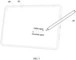
- FIG. 1is a schematic diagram of a scenario to which the embodiments of this application are applicable.
- the scenarioincludes a stylus (stylus) 100, an electronic device 200, and a wireless keyboard 300.
- a tablet computer(tablet) is used as an example of the electronic device 200 for description.
- the stylus 100 and the wireless keyboard 300may provide input to the electronic device 200, and in response to the input, the electronic device 200 performs an operation based on the input of the stylus 100 or the wireless keyboard 300.
- a touch regionmay be provided on the wireless keyboard 300, the stylus 100 may operate in the touch region of the wireless keyboard 300 to provide input to the wireless keyboard 300, and in response to the input, the wireless keyboard 300 may perform an operation based on the input of the stylus 100.
- the stylus 100 and the electronic device 200, the stylus 100 and the wireless keyboard 300, and the electronic device 200 and the wireless keyboard 300may be interconnected through a communication network to implement wireless signal exchange.
- the communication networkmay be, but is not limited to, a Wi-Fi hotspot network, a Wi-Fi peer-to-peer (peer-to-peer, P2P) network, a bluetooth network, a zigbee network, or a near field communication (near field communication, NFC) network, and other near field communication networks.
- the stylus 100may be, but is not limited to, an inductive stylus and a capacitive stylus.
- the electronic device 200has a touchscreen 201.
- an electromagnetic induction boardneeds to be integrated on the touchscreen 201 of the electronic device 200 that interacts with the stylus 100.
- Coilsare distributed on the electromagnetic induction board, and coils are also integrated in the inductive stylus.
- the inductive stylusBased on the principle of electromagnetic induction, within a range of a magnetic field generated by the electromagnetic induction board, the inductive stylus can accumulate and store electric energy with movement of the inductive stylus.
- the inductive stylusmay transmit the accumulated electric energy to the electromagnetic induction board via the coils in the inductive stylus through free oscillation.
- the electromagnetic induction boardmay scan the coils on the electromagnetic induction board based on the electric energy from the inductive stylus to calculate a position of the inductive stylus on the touchscreen 201.
- the touchscreen 201 in the electronic device 200may also be referred to as a touch panel, and the stylus 100 may also be referred to as a stylus pen.
- the capacitive stylusmay include a passive capacitive stylus and an active capacitive stylus.
- the passive capacitive stylusmay be called a passive-type capacitive stylus
- the active capacitive stylusmay be called an active-type capacitive stylus.
- One or more electrodesmay be provided in the active capacitive stylus (for example, in the tip of the stylus), and the active capacitive stylus may transmit a signal through the electrode.
- the stylus 100is an active capacitive stylus
- an electrode arrayneeds to be integrated on the touchscreen 201 of the electronic device 200 that interacts with the stylus 100.
- the electrode arraymay be a capacitive electrode array.
- the electronic device 200may receive a signal from the active capacitive stylus through the electrode array; and when receiving the signal, the electronic device 200 further recognizes a position of the active capacitive stylus on the touchscreen and an inclination angle of the active capacitive stylus based on change of a capacitance value on the touchscreen 201.
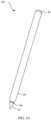
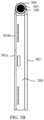
- FIG. 2Ais a schematic structural diagram of a stylus according to an embodiment of this application.
- the stylus 100may include a tip 10, a barrel 20, and a back cover 30.
- the barrel 20is hollowed inside, the tip 10 and the back cover 30 are located at two ends of the barrel 20 respectively, and the back cover 30 and the barrel 20 may be plugged or buckled.
- the tip 10 and the barrel 20may be plugged or buckled.
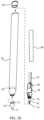
- FIG. 2Bis a schematic diagram of a partially disassembled structure of a stylus according to an embodiment of this application.
- the stylus 100further includes a mainshaft assembly 50, the mainshaft assembly 50 is located in the barrel 20, and the mainshaft assembly 50 is slidably disposed in the barrel 20.
- the mainshaft assembly 50has an external thread 51
- the tip 10includes a writing end 11 and a connecting end 12, where the connecting end 12 of the tip 10 has an internal thread (not shown) matching the external thread 51.
- the connecting end 12 of the tip 10When the mainshaft assembly 50 is assembled into the barrel 20, the connecting end 12 of the tip 10 extends into the barrel 20 and is threadedly connected to the external thread 51 of the mainshaft assembly 50.
- the connecting end 12 of the tip 10may alternatively be detachably connected to the mainshaft assembly 50 through buckling or the like.
- the connecting end 12 of the tip 10 being detachably connected to the mainshaft assembly 50can implement replacement of the tip 10.
- the mainshaft assembly 50is provided with a pressure sensitive assembly 60, part of the pressure sensitive assembly 60 is fixedly connected to a fixing structure in the barrel 20, and part of the pressure sensitive assembly 60 is fixedly connected to the mainshaft assembly 50.
- the circuit board 70detects the pressure on the writing end 11 of the tip 10 based on the deformation of the pressure sensitive assembly 60, so as to control line thickness of the writing end 11 based on the pressure on the writing end 11 of the tip 10.
- the pressure detection of the tip 10includes but is not limited to the foregoing method.
- a pressure sensormay be provided in the writing end 11 of the tip 10, and the pressure on the tip 10 may be detected by the pressure sensor.
- the stylus 100further includes a plurality of electrodes, and the plurality of electrodes may be, for example, a first emission electrode 41, a ground electrode 43, and a second emission electrode 42.
- the first emission electrode 41, the ground electrode 43, and the second emission electrode 42are all electrically connected to the circuit board 70.
- the first emission electrode 41may be located within the tip 10 and close to the writing end 11, and the circuit board 70 may be configured as a control board that can separately provide a signal to the first emission electrode 41 and the second emission electrode 42.
- the first emission electrode 41is configured to emit a first signal, and when the first emission electrode 41 is close to the touchscreen 201 of the electronic device 200, a coupling capacitor may be formed between the first emission electrode 41 and the touchscreen 201 of the electronic device 200, so that the electronic device 200 can receive the first signal.
- the second emission electrode 42is configured to emit a second signal, and the electronic device 200 may determine an angle of inclination of the stylus 100 based on the received second signal.
- the second emission electrode 42may be located on an inner wall of the barrel 20. In an example, the second emission electrode 42 may alternatively be located on the mainshaft assembly 50.
- the ground electrode 43may be located between the first emission electrode 41 and the second emission electrode 42, or the ground electrode 43 may be located around an outer periphery of the first emission electrode 41 and the second emission electrode 42, and the ground electrode 43 is configured to reduce coupling between the first emission electrode 41 and the second emission electrode 42.
- the electronic device 200may determine a position of the stylus 100 (or the tip of the stylus 100) on the touchscreen 201 based on the change of the capacitance value on the touchscreen 201.
- the electronic device 200may obtain the angle of inclination of the stylus 100 by using a double-tip projection method in an inclination angle detection algorithm. Positions of the first emission electrode 41 and the second emission electrode 42 in the stylus 100 are different. Therefore, when the electronic device 200 receives the first signal and the second signal from the stylus 100, capacitance values at the two positions on the touchscreen 201 change.
- the electronic device 200may obtain the angle of inclination of the stylus 100 based on a distance between the first emission electrode 41 and the second emission electrode 42 and a distance between two positions with capacitance values changed on the touchscreen 201. For more details about how the angle of inclination of the stylus 100 is obtained, reference may be made to related descriptions of a dual-tip projection method in the prior art.
- the stylus 100further includes a battery assembly 80, where the battery assembly 80 is configured to provide power to the circuit board 70.
- the battery assembly 80may include a lithium-ion battery, or the battery assembly 80 may include a nickel-chromium battery, an alkaline battery, a nickel-metal hydride battery, or the like.
- the battery included in the battery assembly 80may be a rechargeable battery or a disposable battery.
- the stylus 100supports wireless charging for the battery in the battery assembly 80.
- the electronic device 200may transmit an uplink signal to the stylus 100 through the electrode array integrated on the touchscreen 201.
- the stylus 100may receive the uplink signal through a receiving electrode, and the stylus 100 may transmit a downlink signal through an emission electrode (for example, the first emission electrode 41 and the second emission electrode 42).
- the downlink signalincludes the foregoing first signal and second signal.
- the electronic device 200may determine a position of the tip 10 of the stylus 100 on the touchscreen 201 based on the capacitance value on the touchscreen 201.
- the uplink signal and the downlink signalmay be square wave signals.
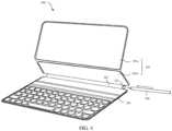
- the wireless keyboard 300may include a first part 301 and a second part 302.
- the wireless keyboard 300may include a keyboard body and a keyboard cover.
- the first part 301may be the keyboard cover
- the second part 302may be the keyboard body.
- the first part 301is configured to hold the electronic device 200, and the second part 302 may be provided with keys, a touch panel, and the like for user operation.
- the first part 301 and the second part 302 of the wireless keyboard 300need to be opened; and when the wireless keyboard 300 is not in use, the first part 301 and the second part 302 of the wireless keyboard 300 can be closed.
- the first part 301 and the second part 302 of the wireless keyboard 300are rotatably connected.
- the first part 301 and the second part 302may be connected through a rotating shaft or a hinge; or in some examples, the first part 301 and the second part 302 are rotatably connected through a flexible material (for example, a leather material or a cloth material).
- first part 301 and the second part 302may be integrally formed, and a joint between the first part 301 and the second part 302 is processed by thinning, so that the joint between the first part 301 and the second part 302 may be bent.
- the first part 301 and the second part 302may be connected in, without limitation to, the foregoing rotatable connection manners.
- the first part 301may include at least two brackets that are rotatably connected.
- the first part 301includes a first bracket 301a and a second bracket 301b.
- the first bracket 301ais rotatably connected to the second bracket 301b.
- both the first bracket 301a and the second bracket 301bmay be used to support the electronic device 200 (refer to FIG. 1 ).
- the first bracket 301asupports the second bracket 301b
- the second bracket 301bsupports the electronic device 200.
- the second bracket 301b and the second part 302are rotatably connected.
- the wireless keyboard 300may be provided with an accommodating portion 303 for accommodating the stylus 100.
- the accommodating portion 303is a cylindrical chamber.
- the stylus 100is inserted into the accommodating chamber in a direction of the arrow in FIG. 4 .
- the second part 302 and the second bracket 301bare rotatably connected by using a connecting portion 304, and the connecting portion 304 is provided with the accommodating portion 303.
- the connecting portion 304may be a rotating shaft.
- FIG. 5Ais a schematic diagram of a stylus being accommodated in an accommodating portion of a wireless keyboard according to an embodiment of this application
- FIG. 5Bis a schematic side view of a stylus being accommodated in an accommodating portion of a wireless keyboard according to an embodiment of this application.
- the accommodating portion 303is a circular chamber, and an inner diameter of the accommodating portion 303 is larger than an outer diameter of the stylus 100.
- a magnetic materialmay be provided on an inner wall of the accommodating portion 303, and a magnetic material may be provided in the stylus 100.
- the stylus 100is adsorbed in the accommodating portion 303 by magnetic adsorption between the magnetic materials.
- the stylus 100may be fastened to the accommodating portion 303 by, but not limited to, magnetic adsorption.
- the stylus 100may alternatively be fastened to the accommodating portion 303 by buckling.
- an eject structuremay be provided in the accommodating portion 303.
- an eject mechanismmay drive that one end of the stylus 100 to eject from the accommodating portion 303.
- FIG. 6is a schematic diagram of a hardware structure of a stylus according to an embodiment of this application.
- the stylus 100may have a processor 110.
- the processor 110may include a storage and processing circuit for supporting an operation of the stylus 100.
- the storage and processing circuitmay include a storage apparatus such as a non-volatile memory (for example, a flash memory or another electrically programmable read-only memory configured as a solid state drive), a volatile memory (for example, a static or dynamic random access memory), and the like.
- the processing circuit in the processor 110may be configured to control the operation of the stylus 100.
- the processing circuitmay be based on one or more microprocessors, microcontrollers, digital signal processors, baseband processors, power management units, audio chips, application specific integrated circuits, and the like.
- the stylus 100may include one or more sensors.
- the sensormay include a pressure sensor 120.
- the pressure sensor 120may be disposed on the writing end 11 of the stylus 100 (as shown in FIG. 2B ).
- the pressure sensor 120may alternatively be disposed in the barrel 20 of the stylus 100, so that after one end of the tip 10 of the stylus 100 is subjected to a force, the other end of the tip 10 moves so that the force acts on the pressure sensor 120.
- the processor 110may adjust, based on the pressure detected by the pressure sensor 120, the thickness of lines written using the tip 10 of the stylus 100.
- the sensorsmay further include an inertial sensor 130.
- the inertial sensor 130may include a three-axis accelerometer and a three-axis gyroscope, and/or other components for measuring movement of the stylus 100, for example, a three-axis magnetometer may be included in the sensor in a nine-axis inertial sensor structure.
- the sensorsmay further include additional sensors, such as a temperature sensor, an ambient light sensor, a light-based proximity sensor, a contact sensor, a magnetic sensor, a pressure sensor, and/or other sensors.
- the stylus 100may include a status indicator 140 such as a light emitting diode and a button 150.
- the status indicator 140is configured to inform a user of a status of the stylus 100.
- the button 150may include a mechanical button and a non-mechanical button, and the button 150 may be configured to collect press-button information from a user.
- the stylus 100may include one or more electrodes 160 (for details, refer to the descriptions in FIG. 2B ).
- One of the electrodes 160may be located at the writing end of the stylus 100, and one of the electrodes 160 may be located inside the tip 10. Reference may be made to the foregoing related descriptions.
- the stylus 100may include a sensing circuit 170.
- the sensing circuit 170may sense capacitive coupling between the electrodes 160 and drive lines of a capacitive touch sensor panel that interacts with the stylus 100.
- the sensing circuit 170may include an amplifier for receiving a capacitance reading from the capacitive touch sensor panel, a clock for generating a demodulation signal, a phase shifter for generating a phase shifted demodulation signal, a mixer for demodulating a capacitance reading by using an in-phase demodulation frequency component, and a mixer for demodulating a capacitance reading by using a quadrature demodulation frequency component. Results of demodulation by the mixers may be used for determining an amplitude proportional to a capacitance, so that the stylus 100 can sense contact with the capacitive touch sensor panel.
- the stylus 100may include a microphone, a speaker, an audio generator, a vibrator, a camera, a data port, and other devices. A user may use these devices to provide commands to control operations of the stylus 100 and the electronic device 200 that interacts with the stylus 100 and receive status information and other output.
- the processor 110may be configured to run software for controlling the operation of the stylus 100 in the stylus 100.
- the software running on the processor 110may process sensor input, button input, and input from other devices to monitor movement of the stylus 100 and other user input.
- the software running on the processor 110may detect a user command and may communicate with the electronic device 200.
- the stylus 100may include a wireless module.
- a bluetooth module 180is used as an example of the wireless module for description.
- the wireless modulemay alternatively be a Wi-Fi hotspot module, a Wi-Fi peer-to-peer module, or the like.
- the bluetooth module 180may include a radio frequency transceiver, such as a transceiver.
- the bluetooth module 180may further include one or more antennas.
- the transceivermay transmit and/or receive a wireless signal by using the antenna.
- the wireless signalmay be a bluetooth signal, a wireless local area network signal, a remote signal such as a cellular telephone signal, a near field communication signal, or other wireless signals based on a type of the wireless module.
- the stylus 100may further include a charging module 190, and the charging module 190 may support charging of the stylus 100 and provide power for the stylus 100.
- the electronic device 200 in this embodiment of this applicationmay be user equipment (user equipment, UE), a terminal (terminal), or the like.
- the electronic device 200may be a portable android device (portable android device, PAD), a personal digital assistant (personal digital assistant, PDA), a handheld device, a computing device, a vehicle-mounted device, or a wearable device with a wireless communication function, a mobile terminal or fixed terminal with a touchscreen such as a virtual reality (virtual reality, VR) terminal device, an augmented reality (augmented reality, AR) terminal device, a wireless terminal in industrial control (industrial control), a wireless terminal in self driving (self driving), a wireless terminal in remote medical (remote medical), a wireless terminal in a smart grid (smart grid), a wireless terminal in transportation safety (transportation safety), a wireless terminal in a smart city (smart city), or a wireless terminal in a smart home (smart home).
- the form of the terminal deviceis not specifically limited in the embodiments of this application.
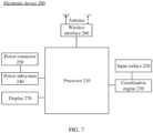
- FIG. 7is a schematic diagram of a hardware structure of an electronic device according to an embodiment of this application.
- the electronic device 200may include a plurality of subsystems. The subsystems cooperate to perform, coordinate, or monitor one or more operations or functions of the electronic device 202.
- the electronic device 200includes a processor 210, an input surface 220, a coordination engine 230, a power subsystem 240, a power connector 250, a wireless interface 260, and a display 270.
- the coordination engine 230may be configured to: communicate with other subsystems of the electronic device 200 and/or process data; communicate with a stylus 100 and/or exchange data; measure and/or obtain output of one or more analog or digital sensors (for example, a touch sensor); measure and/or obtain output of one or more sensor nodes in a sensor node array (for example, a capacitive sensing node array); receive and locate a signal from a tip of the stylus 100 and a ring signal; and locate the stylus 100 based on a position of an intersection area of the tip signal and a position of an intersection area of the ring signal.
- analog or digital sensorsfor example, a touch sensor
- sensor nodes in a sensor node arrayfor example, a capacitive sensing node array
- the coordination engine 230 of the electronic device 200includes or is otherwise communicatively coupled to a sensor layer located under an input surface 220 or integrated with the input surface.
- the coordination engine 230locates the stylus 100 on the input surface 220 by using the sensor layer, and estimates an angular position of the stylus 100 relative to a plane on which the input surface 220 lies, by using the techniques described herein.
- the input surface 220may be referred to as a touchscreen 201.
- the sensor layer of the coordination engine 230 of the electronic device 200is a grid of capacitive sensing nodes arranged in columns and rows. More specifically, an array of column traces is arranged perpendicular to an array of row traces.
- the sensor layermay be separated from other layers of the electronic device, or the sensor layer may be disposed directly on another layer.
- the other layersare, for example but not limited to: a display stack layer, a force sensor layer, a digitizer layer, a polarizer layer, a battery layer, and a structural or decorative shell layer.
- the sensor layercan operate in various modes. If the sensor layer operates in a mutual capacitance mode, the column traces and the row traces form a single capacitive sensing node at each overlapping point (for example, a "vertical" mutual capacitance). If the sensor layer operates in a self-capacitance mode, the column traces and the row traces form two (vertically aligned) capacitive sensing nodes at each overlapping point. In another embodiment, if the sensor layer operates in a mutual capacitance mode, adjacent column traces and/or adjacent row traces may form a single capacitive sensing node (for example, a "horizontal" mutual capacitance).
- the sensor layermay detect presence of the tip 10 of the stylus 100 and/or touch by a user's finger by monitoring changes in capacitance (for example, mutual capacitance or self-capacitance) presented at each capacitive sensing node.
- the coordination engine 230may be configured to detect, by capacitive coupling, tip and ring signals received from the stylus 100 through the sensor layer.
- the tip signal and/or the ring signalmay include specific information and/or data that may be configured to cause the electronic device 200 to recognize the stylus 100. Such information is generally referred to as "stylus identity" information herein. Such information and/or data may be received by the sensor layer, and interpreted, decoded, and/or demodulated by the coordination engine 230.
- the processor 210may use the stylus identity information to simultaneously receive input from more than one stylus.
- the coordination engine 230may be configured to transmit a position and/or an angular position of each of the styluses detected by the coordination engine 230 to the processor 210. In other cases, the coordination engine 230 may also transmit information about relative positions and/or relative angular positions of the plurality of styluses detected by the coordination engine 230 to the processor 210. For example, the coordination engine 230 may notify the processor 210 of a position of a detected first stylus relative to a detected second stylus.
- the tip signal and/or the ring signalmay further include specific information and/or data for enabling the electronic device 200 to identify a specific user.
- Such informationis generally referred to as "user identity” information herein.
- the coordination engine 230may forward the user identity information (if detected and/or recovered) to the processor 210. If the user identity information cannot be recovered from the tip signal and/or the ring signal, the coordination engine 230 may optionally indicate to the processor 210 that the user identity information is unavailable.
- the processor 210can utilize the user identity information (or absence of such information) in any suitable manner, including but not limited to accepting or denying input from the specific user and allowing or denying access to a specific function of the electronic device.
- the processor 210may use the user identity information to simultaneously receive input from more than one user.
- the tip signal and/or ring signalmay include specific information and/or data that may be configured to cause the electronic device 200 to identify a setting or preference of the user or the stylus 100. Such information is generally referred to as "stylus settings" information herein.
- the coordination engine 230may forward the stylus settings information (if detected and/or recovered) to the processor 210. If the stylus settings information cannot be recovered from the tip signal and/or the ring signal, the coordination engine 230 may optionally indicate to the processor 210 that the stylus settings information is unavailable.
- the electronic device 200can utilize the stylus settings information (or absence of such information) in any suitable manner, including but not limited to: applying a setting to the electronic device, applying a setting to a program running on the electronic device, changing a line thickness, a color, a pattern presented by a graphics program of the electronic device, and changing a setting of a video game operated on the electronic device.
- the processor 210may be configured to perform, coordinate, and/or manage functions of the electronic device 200. Such functions may include but are not limited to: communicating with and/or exchanging data with other subsystems of the electronic device 200; communicating with and/or exchanging data with the stylus 100; performing data communication and/or data exchange over a wireless interface; performing data communication and/or data exchange over a wired interface; facilitating exchange of power through a wireless (for example, inductive or resonant) or wired interface; and receiving position(s) and angular position(s) of one or more styluses.
- functionsmay include but are not limited to: communicating with and/or exchanging data with other subsystems of the electronic device 200; communicating with and/or exchanging data with the stylus 100; performing data communication and/or data exchange over a wireless interface; performing data communication and/or data exchange over a wired interface; facilitating exchange of power through a wireless (for example, inductive or resonant) or wired interface; and receiving position(s) and angular position(
- the processor 210may be implemented as any electronic device capable of processing, receiving, or transmitting data or instructions.
- the processormay be a microprocessor, a central processing unit, an application specific integrated circuit, a field programmable gate array, a digital signal processor, an analog circuit, a digital circuit, or a combination of these devices.
- the processormay be a single-threaded or multi-threaded processor.
- the processormay be a single-core or multi-core processor.
- the processor 210may be configured to access a memory in which instructions are stored.
- the instructionsmay be configured to cause the processor to perform, coordinate, or monitor one or more operations or functions of the electronic device 200.
- the instructions stored in the memorymay be configured to control or coordinate operations of other components of the electronic device 200.
- the componentsare, for example but not limited to, another processor, an analog or digital circuit, a volatile or nonvolatile memory module, a display, a speaker, a microphone, a rotary input device, a button, or other physical input devices, a biometric authentication sensor and/or system, a force or touch input/output component, a communication module (for example, a wireless interface and/or a power connector), and/or a haptic device or a haptic feedback device.
- the memorymay further store electronic data for use by the stylus or the processor.
- the memorymay store electronic data or content (for example, a media file, a document, and an application program), a device setting and preference, a timing signal and a control signal, or data, a data structure, or a database for various modules, and a file or configuration related to detecting the tip signal and/or the ring signal.
- the memorymay be configured as any type of memory.
- the memorymay be implemented as a random access memory, a read only memory, a flash memory, a removable memory, other types of storage elements, or a combination of such devices.
- the electronic device 200further includes the power subsystem 240.
- the power subsystem 240may include a battery or other power sources.
- the power subsystem 240may be configured to provide power to the electronic device 200.
- the power subsystem 240may also be coupled to the power connector 250.
- the power connector 250may be any suitable connector or port, and may be configured to receive power from an external power source and/or be configured to provide power to an external load.
- the power connector 250may be configured to recharge a battery within the power subsystem 240.
- the power connector 250may be configured to transfer power stored in (or available to) the power subsystem 240 to the stylus 100.
- the electronic device 200further includes the wireless interface 260 to facilitate electronic communication between the electronic device 200 and the stylus 100.
- the electronic device 200may be configured to communicate with the stylus 100 via a low-energy bluetooth communication interface or a near field communication interface.
- the communication interfacehelps implement electronic communication between the electronic device 200 and an external communication network, a device, or a platform.
- the wireless interface 260may be implemented as one or more wireless interfaces, bluetooth interfaces, near field communication interfaces, magnetic interfaces, universal serial bus interfaces, inductive interfaces, resonant interfaces, capacitive coupling interfaces, Wi-Fi interfaces, TCP/IP interfaces, network communication interfaces, optical interfaces, acoustic interfaces, or any traditional communication interfaces.
- the electronic device 200further includes a display 270.
- the display 270may be located behind the input surface 220, or may be integrated therewith.
- the display 270may be communicatively coupled to the processor 210.
- the processor 210may use the display 270 to present information to a user. In many cases, the processor 210 uses the display 270 to present an interface with which a user may interact. In many cases, the user manipulates the stylus 100 to interact with the interface.
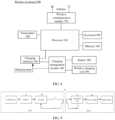
- FIG. 8is a schematic diagram of a hardware structure of a wireless keyboard according to an embodiment of this application.
- the wireless keyboard 300may include a processor 310, a memory 320, a charging interface 330, a charging management module 340, a wireless charging coil 350, a battery 360, a wireless communication module 370, a touch panel 380, and a keyboard 390.
- the processor 310, the memory 320, the charging interface 330, the charging management module 340, the battery 360, the wireless communication module 370, the touch panel 380, the keyboard 390, and the likemay all be disposed on a keyboard body of the wireless keyboard 300 (that is, the second part 302 shown in FIG. 1 ).
- the wireless charging coil 350may be disposed in a connecting portion 304 (as shown in FIG. 4 ) for movably connecting the keyboard body and a bracket. It should be understood that the structure illustrated in this embodiment does not constitute a specific limitation on the wireless keyboard 300. In some other embodiments, the wireless keyboard 300 may include components more or fewer than those shown in the figure, or combine some components, or split some components, or have a different component arrangement.
- the illustrated componentsmay be implemented by hardware, software, or a combination of software and hardware.
- the memory 320may be configured to store program code, such as program code for wirelessly charging the stylus 100.
- the memory 320may further store a bluetooth address that uniquely identifies the wireless keyboard 300.
- the memory 320may further store connection data of an electronic device that has been successfully paired with the wireless keyboard 300 before.
- the connection datamay be a bluetooth address of the electronic device that has been successfully paired with the wireless keyboard 300.
- the bluetooth addressmay be a media access control (media access control, MAC) address.
- the processor 310may be configured to execute the foregoing application program code and invoke relevant modules to implement the functions of the wireless keyboard 300 in the embodiments of this application, for example, to implement a wired charging function, reverse wireless charging function, wireless communication function, and the like of the wireless keyboard 300.
- the processor 310may include one or more processing units, and different processing units may be separate devices or may be integrated into one or more processors 310.
- the processor 310may specifically be an integrated control chip or may include a circuit including various active and/or passive components, and the circuit is configured to perform the functions of the processor 310 described in the embodiments of this application.
- the processor of the wireless keyboard 300may be a microprocessor.
- the wireless communication module 370may be configured to support data exchange between the wireless keyboard 300 and other electronic devices over wireless communication including bluetooth (bluetooth, BT), the global navigation satellite system (global navigation satellite system, GNSS), a wireless local area network (wireless local area networks, WLAN) (for example, a wireless fidelity (wireless fidelity, Wi-Fi) network), frequency modulation (frequency modulation, FM), near field communication (near field communication, NFC), an infrared (infrared, IR) technology, and the like.
- wireless communicationincluding bluetooth (bluetooth, BT), the global navigation satellite system (global navigation satellite system, GNSS), a wireless local area network (wireless local area networks, WLAN) (for example, a wireless fidelity (wireless fidelity, Wi-Fi) network), frequency modulation (frequency modulation, FM), near field communication (near field communication, NFC), an infrared (infrared, IR) technology, and the like.
- the wireless communication module 370may be a bluetooth chip.
- the wireless keyboard 300may be a bluetooth keyboard.
- the wireless keyboard 300may be paired with a bluetooth chip of another electronic device through the bluetooth chip and establish a wireless connection, so as to implement wireless communication between the wireless keyboard 300 and the another electronic device through the wireless connection.
- the wireless communication module 370may further include an antenna.
- the wireless communication module 370receives an electromagnetic wave via the antenna, performs frequency modulation and filtering on an electromagnetic wave signal, and transmits the processed signal to the processor 310.
- the wireless communication module 370may also receive a to-be-sent signal from the processor 310, perform frequency modulation and amplification on the signal, and radiate the signal as an electromagnetic wave using the antenna.
- the wireless keyboard 300may support wired charging.
- the charging management module 340may receive charging input of a wired charger through the charging interface 330.
- the wireless keyboard 300may support forward wireless charging.
- the charging management module 340may receive a wireless charging input through the wireless charging coil 350 of the wireless keyboard 300.
- the charging management module 340is connected to the wireless charging coil 350 through a matching circuit.
- the wireless charging coil 350may be coupled with a wireless charging coil of a wireless charger and induce an alternating electromagnetic field emitted by the wireless charging coil 350 of the wireless charger to generate an alternating current signal.
- the alternating current signal generated by the wireless charging coil 350is transmitted to the charging management module 340 through the matching circuit, so as to charge the battery 360 wirelessly.
- the charging management module 340may further provide power for the wireless keyboard 300 while charging the battery 360.
- the charging management module 340receives input from the battery 360 to provide power for the processor 310, the memory 320, an external memory, the wireless communication module 370, and the like.
- the charging management module 340may be further configured to monitor parameters such as battery capacity of the battery 360, a cycle count of the battery, and a state of health (leakage and impedance) of the battery.
- the charging management module 340may alternatively be disposed in the processor 310.
- the wireless keyboard 300may support reverse wireless charging. Specifically, the charging management module 340 may further receive input from the charging interface 330 or the battery 360 and convert a direct current signal input from the charging interface 330 or the battery 360 into an alternating current signal. The alternating current signal is transmitted to the wireless charging coil 350 through the matching circuit. The wireless charging coil 350 may generate an alternating electromagnetic field upon receiving the alternating current signal. A wireless charging coil of another mobile terminal may perform wireless charging upon sensing the alternating electromagnetic field. That is, the wireless keyboard 300 may further wirelessly charge the another mobile terminal. In an embodiment, the wireless charging coil 350 may be disposed in an accommodating portion 303 of the wireless keyboard 300, and a wireless charging coil is disposed in the barrel 20 of a stylus 100. When the stylus 100 is placed in the accommodating portion 303, the wireless keyboard 300 may charge the stylus 100 through the wireless charging coil 350.
- FIG. 8is a schematic diagram of a hardware structure of the wireless keyboard 300 by using as an example that the matching circuit may be integrated in the charging management module 340.
- the charging interface 330may be configured to provide a wired connection for charging or communication between the wireless keyboard 300 and another electronic device (for example, the wired charger of the wireless keyboard 300).
- a touch sensoris integrated into the touch panel 380.
- a laptopmay receive a control command of a user for the laptop through the touch panel 380 and the keyboard 390.
- the wireless keyboard 300may have more or fewer components than those shown in FIG. 8 , may combine two or more components, or may have a different component configuration.
- a housing of the wireless keyboard 300may be further provided with an accommodating chamber for accommodating the stylus 100.
- the wireless charging coil 350is disposed in the accommodating chamber and is configured to wirelessly charge the stylus 100 after the stylus 100 is accommodated in the accommodating chamber.
- an outer surface of the wireless keyboard 300may further include components such as a key, an indicator light (which may indicate a state such as a battery level, an incoming/outgoing call, or a pairing mode), and a display (which may display prompt information to a user).
- the keymay be a physical key, a touch key (used with the touch sensor), or the like and is configured to trigger operations such as power-on, power-off, start of charging, and end of charging.
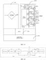
- FIG. 9is a schematic diagram of a possible wireless charging link.
- a portable android device(portable android device, PAD) is used to charge a stylus.
- the PADincludes a PAD battery, a boost (BOOST) chip, a transmit (transport, TX) chip, and a coil.
- the stylusincludes a coil, a receive (receive, RX) chip, a charger (charger) chip, and a battery.
- a voltage of the PAD batteryis input to the boost chip, and the boost chip raises the voltage from the PAD battery and uses the raised voltage to power the TX chip.
- An estimated voltage conversion efficiency in this processis ⁇ 1 .
- the TX chipconverts a direct current signal provided by the boost chip into an alternating current signal through inversion and transmits the signal to the coil, so that the coil sends the signal out.
- An estimated conversion efficiency in this processis ⁇ 2 .
- the coil of the PAD and the coil of the stylusare electromagnetically coupled to transmit energy from the PAD to the stylus.
- a coupling efficiencyis present in the transmission process and an estimated efficiency is ⁇ 3 .
- the RX chipperforms rectification and voltage change on an alternating current signal coupled by the coil of the stylus and outputs a stable direct current signal.
- An estimated efficiency in this processis ⁇ 4 .
- the RX chipoutputs the direct current signal, and the direct current signal needs to be processed by the charger chip to charge the battery of the stylus.
- An estimated efficiency in this processis ⁇ 5 .
- ⁇ total⁇ 1 ⁇ ⁇ 2 ⁇ ⁇ 3 ⁇ ⁇ 4 ⁇ ⁇ 5
- ⁇ totalis about 35%.
- a link efficiencyis relatively low, and the PAD and the stylus overheat severely during charging, resulting in low charging efficiency.
- this embodiment of this applicationprovides a wireless charging circuit to improve overall efficiency of the wireless charging link.
- the RX chip and the charger chipare designed as one component. Energy is coupled from the coil in the stylus, passes through the component, and then is directly output to a battery of the stylus, thereby shortening a wireless charging link and improving link efficiency. This can reduce temperature rise of the stylus during charging and improve charging efficiency.
- the RX chip and the charger chipare designed as one component in this embodiment of this application because the RX chip and the charger chip are found to have identical or similar functional components.
- FIG. 10is a schematic diagram of an internal structure of an RX chip.
- FIG. 11is a schematic diagram of an internal structure of a charger chip.
- the RX chipincludes a rectifier 1001, a low dropout regulator (low dropout regulator, LDO) 1002, a micro-control unit (micro control unit, MCU) 1003, and a protocol encoding/decoding unit 1004.
- a rectifier 1001a low dropout regulator (low dropout regulator, LDO) 1002
- a micro-control unit (micro control unit, MCU) 1003a protocol encoding/decoding unit 1004.
- the rectifier 1001is configured to rectify an alternating current signal coupled by the coil in the stylus to obtain a relatively stable direct current signal, and the direct current signal is used as an input of the LDO 1002.
- the LDO1002is configured to convert the direct current signal after rectification into a standard 5V (which may be certainly any other voltage values, where this is not limited in this embodiment of this application) voltage signal as an input signal of the charger chip.
- a standard 5Vwhich may be certainly any other voltage values, where this is not limited in this embodiment of this application
- the MCU1003is configured to execute software code in the stylus and can be controlled by a register.
- the protocol encoding/decoding unit 1004is configured to communicate with the TX chip.
- the protocol encoding/decoding unit 1004may include an amplitude-shift keying (amplitude-shift keying, ASK) modulation format or a frequency-shift keying (frequency-shift keying, FSK) modulation format, which is not specifically limited in this embodiment of this application.
- the LDO 1002generally includes a field effect transistor 10021, for example, the field effect transistor may include a metal-oxide-semiconductor field-effect transistor (metal-oxide-semiconductor field-effect transistor, MOSFET).
- MOSFETmetal-oxide-semiconductor field-effect transistor
- the charger chipincludes a field effect transistor 1101 (hereinafter referred to as Q1), a field effect transistor 1102 (hereinafter referred to as Q2), and a control circuit for controlling Q1 and Q2.
- Q1field effect transistor 1101
- Q2field effect transistor 1102
- the control circuitmay be implemented by hardware or software, which is not limited in this embodiment of this application.
- Q1may be a MOSFET or the like, and is used as a main LDO to perform voltage stabilization on an input signal VIN from the RX chip and then supply power to a post-stage system.
- Q2may be a MOSFET or the like, and is used to isolate a system power supply from the battery and provides a function of dynamic path management.
- the LDO in the RX chipmay be physically implemented as one MOSFET, and the charger chip may be physically implemented as two MOSFETs, the first MOSFET
- the LDO in the RX chipcan be reused as Q1 in the charger chip, and the RX chip and the charger chip are designed as one component.
- the componentcan implement functions of the RX chip and the charger chip and the wireless charging link can be shortened to improve link efficiency, thereby reducing temperature rise of the stylus during charging and improving charging efficiency.
- the LDO 1002 in FIG. 10 and the field effect transistor 1101 for implementing the LDO function in FIG. 11may alternatively be replaced by a boost circuit (buck) or a switched capacitor (switched capacitor, SC) amplifying circuit for higher power charging.
- the buckmay include two MOSFETs, and the SC may include nine MOSFETs, which are not limited in this embodiment of this application.
- FIG. 12is a schematic diagram of a chip according to an embodiment of this application, and the chip can implement functions of an RX chip and a charger chip.
- the chipincludes a rectifier 1201, an LDO/Buck/SC charger 1202 (which is the foregoing part for implementing functions of LDO/Buck/SC and charger chip, and may be referred to as a charger unit), an MCU1203, and a protocol encoding/decoding unit 1204.
- the rectifier 1201is configured to rectify an alternating current signal coupled by the coil in the stylus to obtain a relatively stable direct current signal, and the direct current signal is used as an input of the LDO/Buck/SC charger 1202.
- the LDO/Buck/SC charger 1202is configured to perform voltage stabilization on a direct current signal obtained through rectification and charge a battery.
- the MCU1203is configured to control wireless communication, the LDO/Buck/SC charger 1202, the protocol encoding/decoding unit 1204, and the like.
- the protocol encoding/decoding unit 1204is configured to communicate with the TX chip.
- the protocol encoding/decoding unit 1204may include an amplitude-shift keying (amplitude-shift keying, ASK) modulation format or a frequency-shift keying (frequency-shift keying, FSK) modulation format, which is not specifically limited in this embodiment of this application.
- the RX chip and the charger chipare designed as one chip, the functions of the RX chip and the charger chip can be implemented and the wireless charging link can be also shortened to improve link efficiency, thereby reducing temperature rise of the stylus during charging and improving charging efficiency.
- FIG. 13 to FIG. 15are schematic diagrams of hardware structures of a chip including an LDO charger, a chip including a buck charger, and a chip including an SC charger respectively.
- the charger unit 1202 in FIG. 12may include an LDO charger 12021, and the LDO charger 12021 includes a first field effect transistor control module 120210, a first field effect transistor 120211, and a second field effect transistor 120212.
- a gate terminal of the first field effect transistor 120211 and a gate terminal of the second field effect transistor 120212are both connected to the first field effect transistor control module 120210, a source terminal of the first field effect transistor 120211 is connected to an output terminal of the rectifier 1201, a drain terminal of the first field effect transistor 120211 is connected to a source terminal of the second field effect transistor 120212, and a drain terminal of the second field effect transistor 120212 is used to charge a battery of the stylus.
- the first field effect transistor control module 120210is configured to control a voltage value of the gate terminal of the first field effect transistor 120211 and that of the gate terminal of the second field effect transistor 120212, so as to control on/off of the first field effect transistor 120211 and the second field effect transistor 120212.
- the first field effect transistor 120211is configured to stabilize a voltage output by the rectifier 1201 to reach a charging voltage required by the stylus
- the second field effect transistor 120212is configured to isolate a system power supply of the chip from the battery of the stylus.
- drain terminal of the first field effect transistor 120211can also be used to provide a voltage output for other devices, for example, the drain terminal of the first field effect transistor 120211 can output Vsys or the like, which is not specifically limited in this embodiment of this application.
- the chipincludes an LDO charger 12021, and the LDO charger 12021 includes a relatively small quantity of field effect transistors and has a relatively simple structure.
- the charger unit 1202 in FIG. 12may include a buck charger 12022, and the buck charger 12022 includes a second field effect transistor control module 120220, a third field effect transistor 120221, a fourth field effect transistor 120222, and a fifth field effect transistor 120223.
- a gate terminal of the third field effect transistor 120221, a gate terminal of the fourth field effect transistor 120222, and a gate terminal of the fifth field effect transistor 120223are all connected to the second field effect transistor control module 120220, a source terminal of the third field effect transistor 120221 is connected to an output terminal of the rectifier 1201, a drain terminal of the third field effect transistor 120221 is connected to a source terminal of the fourth field effect transistor 120222 and one end of an inductor L, a drain terminal of the fourth field effect transistor 120222 is connected to a source terminal of the fifth field effect transistor 120223 and the other end of the inductor L, and a drain terminal of the fifth field effect transistor 120223 is configured to charge a battery of the stylus.
- the second field effect transistor control module 120220is configured to control voltage values of the gate terminal of the third field effect transistor 120221, the gate terminal of the fourth field effect transistor 120222, and the gate terminal of the fifth field effect transistor 120223, so as to control on/off of the third field effect transistor 120221, the fourth field effect transistor 120222, and the fifth field effect transistor 120223.
- the third field effect transistor 120221, the fourth field effect transistor 120222, and the inductor Lcan implement flexible and stable conversion of VIN to obtain a charging voltage required by the stylus; and the fifth field effect transistor 120223 is configured to isolate a system power supply of the chip from the battery of the stylus.
- drain terminal of the fourth field effect transistor 120222can also be used to provide a voltage output for other devices, for example, the drain terminal of the fourth field effect transistor 120222 can output Vsys or the like, which is not specifically limited in this embodiment of this application.
- the chipincludes a buck charger 12022, and the buck charger 12022 has a larger quantity of field effect transistors than the LDO charger 12021.
- the third field effect transistor 120221, the fourth field effect transistor 120222, and the inductor Lflexible and stable voltage conversion of VIN can be implemented to achieve relatively high efficiency.
- the charger unit 1202 in FIG. 12may include an SC charger 12023, and the SC charger 12023 includes a third field effect transistor control module 120230, a sixth field effect transistor 120231, a seventh field effect transistor 120232, an eighth field effect transistor 120233, a ninth field effect transistor 120234, a tenth field effect transistor 120235, an eleventh field effect transistor 120236, a twelfth field effect transistor 120237, a thirteenth field effect transistor 120238, and a fourteenth field effect transistor 120239.
- the SC charger 12023includes a third field effect transistor control module 120230, a sixth field effect transistor 120231, a seventh field effect transistor 120232, an eighth field effect transistor 120233, a ninth field effect transistor 120234, a tenth field effect transistor 120235, an eleventh field effect transistor 120236, a twelfth field effect transistor 120237, a thirteenth field effect transistor 120238, and a fourteenth field effect transistor 120239.
- a gate terminal of each of the sixth field effect transistor 120231, the seventh field effect transistor 120232, the eighth field effect transistor 120233, the ninth field effect transistor 120234, the tenth field effect transistor 120235, the eleventh field effect transistor 120236, the twelfth field effect transistor 120237, the thirteenth field effect transistor 120238, and the fourteenth field effect transistor 120239is connected to the third field effect transistor control module 120230.
- a source terminal of the sixth field effect transistor 120231is connected to an output terminal of the rectifier 1201, a drain terminal of the sixth field effect transistor 120231 is connected to a source terminal of the seventh field effect transistor 120232 and a source terminal of the eleventh field effect transistor 120236, a drain terminal of the seventh field effect transistor 120232 is connected to a source terminal of the eighth field effect transistor 120233 and one end of a capacitor C1, and a drain terminal of the eighth field effect transistor 120233 is connected to a source terminal of the ninth field effect transistor 120234, a drain terminal of the twelfth field effect transistor 120237 is connected to a source terminal of the thirteenth field effect transistor 120238, a drain terminal of the ninth field effect transistor 120234 is connected to a source terminal of the tenth field effect transistor 120235 and the other end of the capacitor C1, a drain terminal of the tenth field effect transistor 120235 and a drain terminal of the fourteenth field effect transistor 120239 are both grounded, a drain terminal of the eleventh field effect transistor 120236 is connected
- the sixth field effect transistor 120231, the seventh field effect transistor 120232, the eighth field effect transistor 120233, the ninth field effect transistor 120234, the tenth field effect transistor 120235, the eleventh field effect transistor 120236, the twelfth field effect transistor 120237, the thirteenth field effect transistor 120238, the fourteenth field effect transistor 120239, the capacitor C1, and the capacitor C2can implement flexible and stable conversion of VIN and isolate the system power supply of the chip from the battery of the stylus.
- FIG. 16is a schematic diagram of a wireless charging link according to an embodiment of this application.
- a PADis configured to charge a stylus.
- the PADincludes a PAD battery, a boost (BOOST) chip, a transmit (transport, TX) chip, and a coil.
- the stylusincludes a coil, a chip 1301 (for implementing RX and charger functions), and a battery.
- a voltage of the PAD batteryis input to the boost chip, and the boost chip raises the voltage from the PAD battery and uses the raised voltage to power the TX chip.
- An estimated voltage conversion efficiency in this processis ⁇ 1 .
- the TX chipconverts a direct current signal provided by the boost chip into an alternating current signal through inversion and transmits the signal to the coil, so that the coil sends the signal out.
- An estimated conversion efficiency in this processis ⁇ 2 .
- the coil of the PAD and the coil of the stylusare electromagnetically coupled to transmit energy from the PAD to the stylus.
- a coupling efficiencyis present in the transmission process and an estimated efficiency is ⁇ 3 .
- the chip 1601performs rectification and voltage change on an alternating current signal coupled by the coil of the stylus, and outputs a stable direct current signal to charge the battery of the stylus.
- An estimated efficiency in this processis ⁇ 6 .
- ⁇ 6 and ⁇ 4 described abovemay be the same or different and are not specifically limited in this embodiment of this application.
- ⁇ total⁇ 1 ⁇ ⁇ 2 ⁇ ⁇ 3 ⁇ ⁇ 6
- the wireless charging link in FIG. 16reduces one efficiency-generating step. Therefore, the wireless charging link in FIG. 16 has higher link efficiency, thereby reducing temperature rise of the stylus during charging and improving charging efficiency.
- the chip 1301 in this embodiment of this applicationmay be an RX chip, a charger chip, or the like.
- functions of the chip 1601include both the RX function and the charger function, and a specific name of the chip 1601 is not limited in this embodiment of this application.
- the PAD in this embodiment of this applicationmay be replaced with a wireless keyboard or the like, and then the stylus can be charged by using the wireless keyboard or the like.
- chip and the wireless charging circuit in the embodiments of this applicationcan also be applied to other applicable wireless charging scenarios, and the wireless charging scenarios are not specifically limited in the embodiments of this application.
Landscapes
- Engineering & Computer Science (AREA)
- Theoretical Computer Science (AREA)
- General Engineering & Computer Science (AREA)
- Physics & Mathematics (AREA)
- General Physics & Mathematics (AREA)
- Human Computer Interaction (AREA)
- Computer Hardware Design (AREA)
- Power Engineering (AREA)
- Computer Networks & Wireless Communication (AREA)
- Signal Processing (AREA)
- Audiology, Speech & Language Pathology (AREA)
- Computational Linguistics (AREA)
- General Health & Medical Sciences (AREA)
- Artificial Intelligence (AREA)
- Health & Medical Sciences (AREA)
- Position Input By Displaying (AREA)
- User Interface Of Digital Computer (AREA)
- Charge And Discharge Circuits For Batteries Or The Like (AREA)
- Telephone Function (AREA)
Description
- This disclosure relates to the field of wireless charging technologies, and in particular, to a wireless charging circuit and a wireless charging system.
- The wireless charging technology originates from the wireless power transfer technology, and its principle is that energy is transferred through magnetic fields between a charger and an electric apparatus. Specifically, the charger can generate an electromagnetic signal, and the electric apparatus can sense the electromagnetic signal, so that the electric apparatus can generate current to charge a battery. Wireless charging is widely applied to existing electronic devices because it does not require additional wires and other accessories.
- For example, in the field of stylus pens, the charger may be a wireless keyboard or an electronic device, and an electric device may be a stylus. The stylus can be wirelessly charged by using the wireless keyboard or electronic device.
- However, existing wireless charging products always have the problem of low charging efficiency.
US 2017/357338 A1 relates to an active stylus equipped with multiple sensors for alleged improved interaction with a touch sensor.EP 3 608 761 A1 relates to an electronic device and a method for displaying affordance for providing charging battery of external device through display.US 2017/025887 A1 relates to an operating method of an electronic device and an electronic device supporting the same.US 2021/044132 A1 relates to an adaptative wireless charging receiver loading.- The object of the present disclosure is to provide a wireless charging circuit and a wireless charging system, so as to shorten a wireless charging link and improve link efficiency According to the invention, this object is achieved with a wireless charging circuit with the technical features of independent claim and with advantageous embodiments defined in dependent claims 2 and 3.
- According to a first aspect according to the invention, an embodiment of this application provides a wireless charging system, including an electronic device and a stylus. The stylus may also be referred to as a stylus pen or the like.
- Specifically, the electronic device is configured to wirelessly charge the stylus; and the stylus includes a wireless charging circuit. The wireless charging circuit includes a first coil, a chip, and a first battery, where the first coil is configured to be coupled to the second coil to obtain an alternating current signal, and the chip is configured to charge the first battery based on the alternating current signal; where a charger unit includes: a voltage-stabilizing charging circuit, a boost charging circuit, or a switched capacitor charging circuit. The chip includes a rectifier, the charger unit, a micro-control unit, and a protocol encoding/decoding unit. The rectifier is configured to rectify an input alternating current signal into a direct current signal; the charger unit is configured to charge the first battery by using the direct current signal from the rectifier; the protocol encoding/decoding unit is configured to communicate with a transmit chip; and the micro-control unit is configured to control the charger unit and the protocol encoding/decoding unit.
- In this embodiment of this application, an RX chip and a charger chip of the stylus can be designed as one component. Energy is coupled from the coil in the stylus, passes through the component, and then is directly output to a battery of the stylus, thereby shortening a wireless charging link and improving link efficiency. This can reduce temperature rise of the stylus during charging and improve charging efficiency.
- In the invention, the voltage-stabilizing charging circuit includes a first field effect transistor control module, a first field effect transistor, and a second field effect transistor, where a gate terminal of the first field effect transistor and a gate terminal of the second field effect transistor are both connected to the first field effect transistor control module, a source terminal of the first field effect transistor is connected to an output terminal of the rectifier, a drain terminal of the first field effect transistor is connected to a source terminal of the second field effect transistor, and a drain terminal of the second field effect transistor is used to charge a battery of the stylus.
- In this way, the chip includes an LDO charger, and the LDO charger includes a relatively small quantity of field effect transistors and has a relatively simple structure.
- In a possible design not claimed, the voltage-stabilizing charging circuit includes a second field effect transistor control module, a third field effect transistor, a fourth field effect transistor, and a fifth field effect transistor, where a gate terminal of the third field effect transistor, a gate terminal of the fourth field effect transistor, and a gate terminal of the fifth field effect transistor are all connected to the second field effect transistor control module, a source terminal of the third field effect transistor is connected to an output terminal of the rectifier, a drain terminal of the third field effect transistor is connected to a source terminal of the fourth field effect transistor and one end of an inductor L, a drain terminal of the fourth field effect transistor is connected to a source terminal of the fifth field effect transistor and the other end of the inductor L, and a drain terminal of the fifth field effect transistor is configured to charge a battery of the stylus.
- In this way, the chip includes a buck charger, and the buck charger has a larger quantity of field effect transistors than the LDO charger. With the third field effect transistor, the fourth field effect transistor, and the inductor L, flexible and stable voltage conversion can be implemented, achieving relatively high efficiency.
- In a possible design not claimed, the voltage-stabilizing charging circuit includes a third field effect transistor control module, a sixth field effect transistor, a seventh field effect transistor, an eighth field effect transistor, a ninth field effect transistor, a tenth field effect transistor, an eleventh field effect transistor, a twelfth field effect transistor, a thirteenth field effect transistor, and a fourteenth field effect transistor.
- A gate terminal of each of the sixth field effect transistor, the seventh field effect transistor, the eighth field effect transistor, the ninth field effect transistor, the tenth field effect transistor, the eleventh field effect transistor, the twelfth field effect transistor, the thirteenth field effect transistor, and the fourteenth field effect transistor is connected to the third field effect transistor control module; and a source terminal of the sixth field effect transistor is connected to an output terminal of the rectifier, a drain terminal of the sixth field effect transistor is connected to a source terminal of the seventh field effect transistor and a source terminal of the eleventh field effect transistor, a drain terminal of the seventh field effect transistor is connected to a source terminal of the eighth field effect transistor and one end of a capacitor C1, and a drain terminal of the eighth field effect transistor is connected to a source terminal of the ninth field effect transistor, a drain terminal of the twelfth field effect transistor is connected to a source terminal of the thirteenth field effect transistor, a drain terminal of the ninth field effect transistor is connected to a source terminal of the tenth field effect transistor and the other end of the capacitor C1, a drain terminal of the tenth field effect transistor and a drain terminal of the fourteenth field effect transistor are both grounded, a drain terminal of the eleventh field effect transistor is connected to a source terminal of the twelfth field effect transistor and one end of a capacitor C2, a drain terminal of the twelfth field effect transistor is connected to a source terminal of the thirteenth field effect transistor, and a drain terminal of the thirteenth field effect transistor is connected to a source terminal of the fourteenth field effect transistor and the other end of the capacitor C2, where the drain terminal of the eighth field effect transistor being connected to the drain terminal of the twelfth field effect transistor is used to charge a battery of the stylus.
- In a possible design not claimed, the electronic device includes a second battery, a boost chip, a transmit chip, and the second coil, where the second battery is configured to input voltage to the boost chip; the boost chip is configured to boost the voltage to obtain a first direct current signal; the transmit chip is configured to invert the first direct current signal into a first alternating current signal, and transmit the first alternating current signal to the second coil; and the second coil is configured to be coupled to the first coil by using the first alternating current signal. In this way, the electronic device can be used to charge the stylus.
- In one possible design, the electronic device is a tablet computer or a wireless keyboard, applied to use scenarios of the stylus.
- According to a second aspect not claimed, an embodiment of this application provides a chip, including a rectifier, a charger unit, a micro-control unit, and a protocol encoding/decoding unit. The rectifier is configured to rectify an input alternating current signal into a direct current signal; the charger unit is configured to charge a battery by using the direct current signal from the rectifier, where the charger unit includes a voltage-stabilizing charging circuit, a boost charging circuit, or a switched capacitor charging circuit; the protocol encoding/decoding unit is configured to communicate with a transmit chip; and the micro-control unit is configured to control the charger unit and the protocol encoding/decoding unit.
- In a possible design, the voltage-stabilizing charging circuit includes a first field effect transistor control module, a first field effect transistor, and a second field effect transistor, where a gate terminal of the first field effect transistor and a gate terminal of the second field effect transistor are both connected to the first field effect transistor control module, a source terminal of the first field effect transistor is connected to an output terminal of the rectifier, a drain terminal of the first field effect transistor is connected to a source terminal of the second field effect transistor, and a drain terminal of the second field effect transistor is used to charge a battery of the stylus.
- In a possible design, the voltage-stabilizing charging circuit includes a second field effect transistor control module, a third field effect transistor, a fourth field effect transistor, and a fifth field effect transistor, where a gate terminal of the third field effect transistor, a gate terminal of the fourth field effect transistor, and a gate terminal of the fifth field effect transistor are all connected to the second field effect transistor control module, a source terminal of the third field effect transistor is connected to an output terminal of the rectifier, a drain terminal of the third field effect transistor is connected to a source terminal of the fourth field effect transistor and one end of an inductor L, a drain terminal of the fourth field effect transistor is connected to a source terminal of the fifth field effect transistor and the other end of the inductor L, and a drain terminal of the fifth field effect transistor is configured to charge a battery of the stylus.
- In a possible design, the voltage-stabilizing charging circuit includes a third field effect transistor control module, a sixth field effect transistor, a seventh field effect transistor, an eighth field effect transistor, a ninth field effect transistor, a tenth field effect transistor, an eleventh field effect transistor, a twelfth field effect transistor, a thirteenth field effect transistor, and a fourteenth field effect transistor. A gate terminal of each of the sixth field effect transistor, the seventh field effect transistor, the eighth field effect transistor, the ninth field effect transistor, the tenth field effect transistor, the eleventh field effect transistor, the twelfth field effect transistor, the thirteenth field effect transistor, and the fourteenth field effect transistor is connected to the third field effect transistor control module; and a source terminal of the sixth field effect transistor is connected to an output terminal of the rectifier, a drain terminal of the sixth field effect transistor is connected to a source terminal of the seventh field effect transistor and a source terminal of the eleventh field effect transistor, a drain terminal of the seventh field effect transistor is connected to a source terminal of the eighth field effect transistor and one end of a capacitor C1, and a drain terminal of the eighth field effect transistor is connected to a source terminal of the ninth field effect transistor, a drain terminal of the twelfth field effect transistor is connected to a source terminal of the thirteenth field effect transistor, a drain terminal of the ninth field effect transistor is connected to a source terminal of the tenth field effect transistor and the other end of the capacitor C1, a drain terminal of the tenth field effect transistor and a drain terminal of the fourteenth field effect transistor are both grounded, a drain terminal of the eleventh field effect transistor is connected to a source terminal of the twelfth field effect transistor and one end of a capacitor C2, a drain terminal of the twelfth field effect transistor is connected to a source terminal of the thirteenth field effect transistor, and a drain terminal of the thirteenth field effect transistor is connected to a source terminal of the fourteenth field effect transistor and the other end of the capacitor C2, where the drain terminal of the eighth field effect transistor being connected to the drain terminal of the twelfth field effect transistor is used to charge a battery of the stylus.
- According to a third aspect according to the invention, an embodiment of this application provides a wireless charging circuit applied to a stylus. The wireless charging circuit includes a first coil, a chip, and a first battery, where the first coil is configured to be coupled to the second coil to obtain an alternating current signal, and the chip is configured to charge the first battery based on the alternating current signal. The chip includes a rectifier, a charger unit, a micro-control unit, and a protocol encoding/decoding unit. The rectifier is configured to rectify an input alternating current signal into a direct current signal. The charger unit is configured to charge the first battery by using the direct current signal from the rectifier, and the charger unit includes a voltage-stabilizing charging circuit, a boost charging circuit, or a switched capacitor charging circuit. The protocol encoding/decoding unit is configured to communicate with a transmit chip. The micro-control unit is configured to control the charger unit and the protocol encoding/decoding unit.
- In the invention, the voltage-stabilizing charging circuit includes a first field effect transistor control module, a first field effect transistor, and a second field effect transistor, where a gate terminal of the first field effect transistor and a gate terminal of the second field effect transistor are both connected to the first field effect transistor control module, a source terminal of the first field effect transistor is connected to an output terminal of the rectifier, a drain terminal of the first field effect transistor is connected to a source terminal of the second field effect transistor, and a drain terminal of the second field effect transistor is used to charge a battery of the stylus.
- In a possible design not claimed, the voltage-stabilizing charging circuit includes a second field effect transistor control module, a third field effect transistor, a fourth field effect transistor, and a fifth field effect transistor, where a gate terminal of the third field effect transistor, a gate terminal of the fourth field effect transistor, and a gate terminal of the fifth field effect transistor are all connected to the second field effect transistor control module, a source terminal of the third field effect transistor is connected to an output terminal of the rectifier, a drain terminal of the third field effect transistor is connected to a source terminal of the fourth field effect transistor and one end of an inductor L, a drain terminal of the fourth field effect transistor is connected to a source terminal of the fifth field effect transistor and the other end of the inductor L, and a drain terminal of the fifth field effect transistor is configured to charge a battery of the stylus.
- In a possible design not claimed, the voltage-stabilizing charging circuit includes a third field effect transistor control module, a sixth field effect transistor, a seventh field effect transistor, an eighth field effect transistor, a ninth field effect transistor, a tenth field effect transistor, an eleventh field effect transistor, a twelfth field effect transistor, a thirteenth field effect transistor, and a fourteenth field effect transistor. A gate terminal of each of the sixth field effect transistor, the seventh field effect transistor, the eighth field effect transistor, the ninth field effect transistor, the tenth field effect transistor, the eleventh field effect transistor, the twelfth field effect transistor, the thirteenth field effect transistor, and the fourteenth field effect transistor is connected to the third field effect transistor control module; and a source terminal of the sixth field effect transistor is connected to an output terminal of the rectifier, a drain terminal of the sixth field effect transistor is connected to a source terminal of the seventh field effect transistor and a source terminal of the eleventh field effect transistor, a drain terminal of the seventh field effect transistor is connected to a source terminal of the eighth field effect transistor and one end of a capacitor C1, and a drain terminal of the eighth field effect transistor is connected to a source terminal of the ninth field effect transistor, a drain terminal of the twelfth field effect transistor is connected to a source terminal of the thirteenth field effect transistor, a drain terminal of the ninth field effect transistor is connected to a source terminal of the tenth field effect transistor and the other end of the capacitor C1, a drain terminal of the tenth field effect transistor and a drain terminal of the fourteenth field effect transistor are both grounded, a drain terminal of the eleventh field effect transistor is connected to a source terminal of the twelfth field effect transistor and one end of a capacitor C2, a drain terminal of the twelfth field effect transistor is connected to a source terminal of the thirteenth field effect transistor, and a drain terminal of the thirteenth field effect transistor is connected to a source terminal of the fourteenth field effect transistor and the other end of the capacitor C2, where the drain terminal of the eighth field effect transistor being connected to the drain terminal of the twelfth field effect transistor is used to charge a battery of the stylus.
- For beneficial effects in the second aspect, the third aspect, and the possible designs thereof, reference may be made to beneficial effects in the first aspect and the possible implementations of the first aspect, and details are not repeated herein.
FIG. 1 is a schematic diagram of a scenario to which embodiments of this application are applicable;FIG. 2A is a schematic structural diagram of a stylus according to an embodiment of this application;FIG. 2B is a schematic diagram of a partially disassembled structure of a stylus according to an embodiment of this application;FIG. 3 is a schematic diagram of interaction between a stylus and an electronic device according to an embodiment of this application;FIG. 4 is a schematic diagram of assembly of a stylus and a wireless keyboard according to an embodiment of this application;FIG. 5A is a schematic diagram of a stylus being accommodated in an accommodating portion of a wireless keyboard according to an embodiment of this application;FIG. 5B is a schematic side view of a stylus being accommodated in an accommodating portion of a wireless keyboard according to an embodiment of this application;FIG. 6 is a schematic diagram of a hardware structure of a stylus according to an embodiment of this application;FIG. 7 is a schematic diagram of a hardware structure of an electronic device according to an embodiment of this application;FIG. 8 is a schematic diagram of a hardware structure of a wireless keyboard according to an embodiment of this application;FIG. 9 is a schematic diagram of a wireless charging link in a possible design;FIG. 10 is a schematic diagram of a hardware structure of an RX chip in a possible design;FIG. 11 is a schematic diagram of a hardware structure of a charger chip in a possible design;FIG. 12 is a schematic diagram of a hardware structure of a chip according to an embodiment of this application;FIG. 13 is a schematic diagram of a specific hardware structure of a chip according to an embodiment of this application;FIG. 14 is a schematic diagram of a specific hardware structure of a chip according to a non-claimed embodiment of this application;FIG. 15 is a schematic diagram of a specific hardware structure of a chip according to a non-claimed embodiment of this application; andFIG. 16 is a schematic diagram of a wireless charging link according to an embodiment of this application.- In the following description, features which in the above summary of the invention have been marked as "not claimed" are also hereinafter, when they are described and explained with reference to the drawings, to be understood as "not claimed" or "not part of the invention".
- Unless otherwise specified, "plurality of" in this specification indicates two or more. The term "and/or" in this specification describes only an association relationship for describing associated objects and represents that three relationships may exist. For example, A and/or B may represent the following three cases: A alone, both A and B, and B alone. In addition, the character "/" in this specification generally represents an "or" relationship between associated objects. In a formula, the character "/" indicates a "division" relationship between the associated objects.
- It should be understood that digital numbers in the embodiments of this application are merely for differentiation for ease of description and are not intended to limit the scope of the embodiments of this application.
- It should be understood that, in the embodiments of this application, sequence numbers of the foregoing processes do not indicate execution sequences. The execution sequences of the processes should be determined according to functions and internal logic of the processes and should not be construed as any limitation on the implementation processes of the embodiments of this application.
FIG. 1 is a schematic diagram of a scenario to which the embodiments of this application are applicable. Referring toFIG. 1 , the scenario includes a stylus (stylus) 100, anelectronic device 200, and awireless keyboard 300. InFIG. 1 , a tablet computer (tablet) is used as an example of theelectronic device 200 for description. Thestylus 100 and thewireless keyboard 300 may provide input to theelectronic device 200, and in response to the input, theelectronic device 200 performs an operation based on the input of thestylus 100 or thewireless keyboard 300. A touch region may be provided on thewireless keyboard 300, thestylus 100 may operate in the touch region of thewireless keyboard 300 to provide input to thewireless keyboard 300, and in response to the input, thewireless keyboard 300 may perform an operation based on the input of thestylus 100. In an embodiment, thestylus 100 and theelectronic device 200, thestylus 100 and thewireless keyboard 300, and theelectronic device 200 and thewireless keyboard 300 may be interconnected through a communication network to implement wireless signal exchange. The communication network may be, but is not limited to, a Wi-Fi hotspot network, a Wi-Fi peer-to-peer (peer-to-peer, P2P) network, a bluetooth network, a zigbee network, or a near field communication (near field communication, NFC) network, and other near field communication networks.- The
stylus 100 may be, but is not limited to, an inductive stylus and a capacitive stylus. Theelectronic device 200 has atouchscreen 201. When thestylus 100 is an inductive stylus, an electromagnetic induction board needs to be integrated on thetouchscreen 201 of theelectronic device 200 that interacts with thestylus 100. Coils are distributed on the electromagnetic induction board, and coils are also integrated in the inductive stylus. Based on the principle of electromagnetic induction, within a range of a magnetic field generated by the electromagnetic induction board, the inductive stylus can accumulate and store electric energy with movement of the inductive stylus. The inductive stylus may transmit the accumulated electric energy to the electromagnetic induction board via the coils in the inductive stylus through free oscillation. The electromagnetic induction board may scan the coils on the electromagnetic induction board based on the electric energy from the inductive stylus to calculate a position of the inductive stylus on thetouchscreen 201. Thetouchscreen 201 in theelectronic device 200 may also be referred to as a touch panel, and thestylus 100 may also be referred to as a stylus pen. - The capacitive stylus may include a passive capacitive stylus and an active capacitive stylus. The passive capacitive stylus may be called a passive-type capacitive stylus, and the active capacitive stylus may be called an active-type capacitive stylus.
- One or more electrodes may be provided in the active capacitive stylus (for example, in the tip of the stylus), and the active capacitive stylus may transmit a signal through the electrode. When the
stylus 100 is an active capacitive stylus, an electrode array needs to be integrated on thetouchscreen 201 of theelectronic device 200 that interacts with thestylus 100. In an embodiment, the electrode array may be a capacitive electrode array. Theelectronic device 200 may receive a signal from the active capacitive stylus through the electrode array; and when receiving the signal, theelectronic device 200 further recognizes a position of the active capacitive stylus on the touchscreen and an inclination angle of the active capacitive stylus based on change of a capacitance value on thetouchscreen 201. FIG. 2A is a schematic structural diagram of a stylus according to an embodiment of this application. Referring toFIG. 2A , thestylus 100 may include atip 10, abarrel 20, and aback cover 30. Thebarrel 20 is hollowed inside, thetip 10 and theback cover 30 are located at two ends of thebarrel 20 respectively, and theback cover 30 and thebarrel 20 may be plugged or buckled. For a matching relationship between thetip 10 and thebarrel 20, refer to the description inFIG. 2B .FIG. 2B is a schematic diagram of a partially disassembled structure of a stylus according to an embodiment of this application. Referring toFIG. 2B , thestylus 100 further includes amainshaft assembly 50, themainshaft assembly 50 is located in thebarrel 20, and themainshaft assembly 50 is slidably disposed in thebarrel 20. Themainshaft assembly 50 has anexternal thread 51, and thetip 10 includes a writingend 11 and a connectingend 12, where the connectingend 12 of thetip 10 has an internal thread (not shown) matching theexternal thread 51.- When the
mainshaft assembly 50 is assembled into thebarrel 20, the connectingend 12 of thetip 10 extends into thebarrel 20 and is threadedly connected to theexternal thread 51 of themainshaft assembly 50. In some other examples, the connectingend 12 of thetip 10 may alternatively be detachably connected to themainshaft assembly 50 through buckling or the like. The connectingend 12 of thetip 10 being detachably connected to themainshaft assembly 50 can implement replacement of thetip 10. - For detection of a pressure on the writing
end 11 of thetip 10, as shown inFIG. 2A , there is agap 10a between thetip 10 and thebarrel 20, which can ensure that when the writingend 11 of thetip 10 is subjected to external force, thetip 10 may move toward thebarrel 20, and the movement of thetip 10 drives themainshaft assembly 50 to move within thebarrel 20. For detection of the external force, as shown inFIG. 2B , themainshaft assembly 50 is provided with a pressuresensitive assembly 60, part of the pressuresensitive assembly 60 is fixedly connected to a fixing structure in thebarrel 20, and part of the pressuresensitive assembly 60 is fixedly connected to themainshaft assembly 50. In this way, when themainshaft assembly 50 moves with thetip 10, because part of the pressuresensitive assembly 60 is fixedly connected to the fixing structure in thebarrel 20, movement of themainshaft assembly 50 causes the pressuresensitive assembly 60 to deform, and deformation of the pressuresensitive assembly 60 is transferred to a circuit board 70 (for example, the pressuresensitive assembly 60 and thecircuit board 70 may be electrically connected via a wire or a flexible circuit board), thecircuit board 70 detects the pressure on the writingend 11 of thetip 10 based on the deformation of the pressuresensitive assembly 60, so as to control line thickness of the writingend 11 based on the pressure on the writingend 11 of thetip 10. - It should be noted that the pressure detection of the
tip 10 includes but is not limited to the foregoing method. For example, a pressure sensor may be provided in the writingend 11 of thetip 10, and the pressure on thetip 10 may be detected by the pressure sensor. - In this embodiment, as shown in
FIG. 2B , thestylus 100 further includes a plurality of electrodes, and the plurality of electrodes may be, for example, afirst emission electrode 41, aground electrode 43, and asecond emission electrode 42. Thefirst emission electrode 41, theground electrode 43, and thesecond emission electrode 42 are all electrically connected to thecircuit board 70. Thefirst emission electrode 41 may be located within thetip 10 and close to the writingend 11, and thecircuit board 70 may be configured as a control board that can separately provide a signal to thefirst emission electrode 41 and thesecond emission electrode 42. Thefirst emission electrode 41 is configured to emit a first signal, and when thefirst emission electrode 41 is close to thetouchscreen 201 of theelectronic device 200, a coupling capacitor may be formed between thefirst emission electrode 41 and thetouchscreen 201 of theelectronic device 200, so that theelectronic device 200 can receive the first signal. Thesecond emission electrode 42 is configured to emit a second signal, and theelectronic device 200 may determine an angle of inclination of thestylus 100 based on the received second signal. In this embodiment of this application, thesecond emission electrode 42 may be located on an inner wall of thebarrel 20. In an example, thesecond emission electrode 42 may alternatively be located on themainshaft assembly 50. - The
ground electrode 43 may be located between thefirst emission electrode 41 and thesecond emission electrode 42, or theground electrode 43 may be located around an outer periphery of thefirst emission electrode 41 and thesecond emission electrode 42, and theground electrode 43 is configured to reduce coupling between thefirst emission electrode 41 and thesecond emission electrode 42. - When the
electronic device 200 receives the first signal from thestylus 100, a capacitance value at a corresponding position of thetouchscreen 201 changes. Accordingly, theelectronic device 200 may determine a position of the stylus 100 (or the tip of the stylus 100) on thetouchscreen 201 based on the change of the capacitance value on thetouchscreen 201. In addition, theelectronic device 200 may obtain the angle of inclination of thestylus 100 by using a double-tip projection method in an inclination angle detection algorithm. Positions of thefirst emission electrode 41 and thesecond emission electrode 42 in thestylus 100 are different. Therefore, when theelectronic device 200 receives the first signal and the second signal from thestylus 100, capacitance values at the two positions on thetouchscreen 201 change. Theelectronic device 200 may obtain the angle of inclination of thestylus 100 based on a distance between thefirst emission electrode 41 and thesecond emission electrode 42 and a distance between two positions with capacitance values changed on thetouchscreen 201. For more details about how the angle of inclination of thestylus 100 is obtained, reference may be made to related descriptions of a dual-tip projection method in the prior art. - In this embodiment of this application, as shown in
FIG. 2B , thestylus 100 further includes abattery assembly 80, where thebattery assembly 80 is configured to provide power to thecircuit board 70. Thebattery assembly 80 may include a lithium-ion battery, or thebattery assembly 80 may include a nickel-chromium battery, an alkaline battery, a nickel-metal hydride battery, or the like. In an embodiment, the battery included in thebattery assembly 80 may be a rechargeable battery or a disposable battery. When the battery included in thebattery assembly 80 is a rechargeable battery, thestylus 100 supports wireless charging for the battery in thebattery assembly 80. - When the
stylus 100 is an active capacitive stylus, referring toFIG. 3 , after theelectronic device 200 and thestylus 100 are wirelessly connected, theelectronic device 200 may transmit an uplink signal to thestylus 100 through the electrode array integrated on thetouchscreen 201. Thestylus 100 may receive the uplink signal through a receiving electrode, and thestylus 100 may transmit a downlink signal through an emission electrode (for example, thefirst emission electrode 41 and the second emission electrode 42). The downlink signal includes the foregoing first signal and second signal. When thetip 10 of thestylus 100 comes in contact with thetouchscreen 201, a capacitance value at a corresponding position of thetouchscreen 201 changes, and theelectronic device 200 may determine a position of thetip 10 of thestylus 100 on thetouchscreen 201 based on the capacitance value on thetouchscreen 201. In an embodiment, the uplink signal and the downlink signal may be square wave signals. - In an embodiment, referring to
FIG. 4 , thewireless keyboard 300 may include afirst part 301 and asecond part 302. For example, thewireless keyboard 300 may include a keyboard body and a keyboard cover. Thefirst part 301 may be the keyboard cover, and thesecond part 302 may be the keyboard body. Thefirst part 301 is configured to hold theelectronic device 200, and thesecond part 302 may be provided with keys, a touch panel, and the like for user operation. - When the
wireless keyboard 300 is in use, thefirst part 301 and thesecond part 302 of thewireless keyboard 300 need to be opened; and when thewireless keyboard 300 is not in use, thefirst part 301 and thesecond part 302 of thewireless keyboard 300 can be closed. In an embodiment, thefirst part 301 and thesecond part 302 of thewireless keyboard 300 are rotatably connected. For example, thefirst part 301 and thesecond part 302 may be connected through a rotating shaft or a hinge; or in some examples, thefirst part 301 and thesecond part 302 are rotatably connected through a flexible material (for example, a leather material or a cloth material). Alternatively, in some examples, thefirst part 301 and thesecond part 302 may be integrally formed, and a joint between thefirst part 301 and thesecond part 302 is processed by thinning, so that the joint between thefirst part 301 and thesecond part 302 may be bent. Thefirst part 301 and thesecond part 302 may be connected in, without limitation to, the foregoing rotatable connection manners. - The
first part 301 may include at least two brackets that are rotatably connected. For example, referring toFIG. 4 , thefirst part 301 includes afirst bracket 301a and asecond bracket 301b. Thefirst bracket 301a is rotatably connected to thesecond bracket 301b. During use of theelectronic device 200, both thefirst bracket 301a and thesecond bracket 301b may be used to support the electronic device 200 (refer toFIG. 1 ). Alternatively, thefirst bracket 301a supports thesecond bracket 301b, and thesecond bracket 301b supports theelectronic device 200. Referring toFIG. 4 , thesecond bracket 301b and thesecond part 302 are rotatably connected. - Referring to
FIG. 4 , to accommodate thestylus 100, thewireless keyboard 300 may be provided with anaccommodating portion 303 for accommodating thestylus 100. Referring toFIG. 4 , theaccommodating portion 303 is a cylindrical chamber. When being accommodated, thestylus 100 is inserted into the accommodating chamber in a direction of the arrow inFIG. 4 . In this embodiment, referring toFIG. 4 , thesecond part 302 and thesecond bracket 301b are rotatably connected by using a connectingportion 304, and the connectingportion 304 is provided with theaccommodating portion 303. The connectingportion 304 may be a rotating shaft. FIG. 5A is a schematic diagram of a stylus being accommodated in an accommodating portion of a wireless keyboard according to an embodiment of this application; andFIG. 5B is a schematic side view of a stylus being accommodated in an accommodating portion of a wireless keyboard according to an embodiment of this application. Referring toFIG. 5B , theaccommodating portion 303 is a circular chamber, and an inner diameter of theaccommodating portion 303 is larger than an outer diameter of thestylus 100.- To prevent the
stylus 100 from dropping from theaccommodating portion 303, in an embodiment, a magnetic material may be provided on an inner wall of theaccommodating portion 303, and a magnetic material may be provided in thestylus 100. Thestylus 100 is adsorbed in theaccommodating portion 303 by magnetic adsorption between the magnetic materials. Certainly, in some examples, thestylus 100 may be fastened to theaccommodating portion 303 by, but not limited to, magnetic adsorption. For example, thestylus 100 may alternatively be fastened to theaccommodating portion 303 by buckling. - To help the
stylus 100 to be taken out of theaccommodating portion 303, an eject structure may be provided in theaccommodating portion 303. For example, when one end of thestylus 100 is pressed, an eject mechanism may drive that one end of thestylus 100 to eject from theaccommodating portion 303. FIG. 6 is a schematic diagram of a hardware structure of a stylus according to an embodiment of this application. Referring toFIG. 6 , thestylus 100 may have aprocessor 110. Theprocessor 110 may include a storage and processing circuit for supporting an operation of thestylus 100. The storage and processing circuit may include a storage apparatus such as a non-volatile memory (for example, a flash memory or another electrically programmable read-only memory configured as a solid state drive), a volatile memory (for example, a static or dynamic random access memory), and the like. The processing circuit in theprocessor 110 may be configured to control the operation of thestylus 100. The processing circuit may be based on one or more microprocessors, microcontrollers, digital signal processors, baseband processors, power management units, audio chips, application specific integrated circuits, and the like.- The
stylus 100 may include one or more sensors. For example, the sensor may include apressure sensor 120. Thepressure sensor 120 may be disposed on the writingend 11 of the stylus 100 (as shown inFIG. 2B ). Certainly, thepressure sensor 120 may alternatively be disposed in thebarrel 20 of thestylus 100, so that after one end of thetip 10 of thestylus 100 is subjected to a force, the other end of thetip 10 moves so that the force acts on thepressure sensor 120. In an embodiment, theprocessor 110 may adjust, based on the pressure detected by thepressure sensor 120, the thickness of lines written using thetip 10 of thestylus 100. - The sensors may further include an
inertial sensor 130. Theinertial sensor 130 may include a three-axis accelerometer and a three-axis gyroscope, and/or other components for measuring movement of thestylus 100, for example, a three-axis magnetometer may be included in the sensor in a nine-axis inertial sensor structure. The sensors may further include additional sensors, such as a temperature sensor, an ambient light sensor, a light-based proximity sensor, a contact sensor, a magnetic sensor, a pressure sensor, and/or other sensors. - The
stylus 100 may include a status indicator 140 such as a light emitting diode and abutton 150. The status indicator 140 is configured to inform a user of a status of thestylus 100. Thebutton 150 may include a mechanical button and a non-mechanical button, and thebutton 150 may be configured to collect press-button information from a user. - In this embodiment of this application, the
stylus 100 may include one or more electrodes 160 (for details, refer to the descriptions inFIG. 2B ). One of theelectrodes 160 may be located at the writing end of thestylus 100, and one of theelectrodes 160 may be located inside thetip 10. Reference may be made to the foregoing related descriptions. - The
stylus 100 may include asensing circuit 170. Thesensing circuit 170 may sense capacitive coupling between theelectrodes 160 and drive lines of a capacitive touch sensor panel that interacts with thestylus 100. Thesensing circuit 170 may include an amplifier for receiving a capacitance reading from the capacitive touch sensor panel, a clock for generating a demodulation signal, a phase shifter for generating a phase shifted demodulation signal, a mixer for demodulating a capacitance reading by using an in-phase demodulation frequency component, and a mixer for demodulating a capacitance reading by using a quadrature demodulation frequency component. Results of demodulation by the mixers may be used for determining an amplitude proportional to a capacitance, so that thestylus 100 can sense contact with the capacitive touch sensor panel. - It can be understood that, according to an actual need, the
stylus 100 may include a microphone, a speaker, an audio generator, a vibrator, a camera, a data port, and other devices. A user may use these devices to provide commands to control operations of thestylus 100 and theelectronic device 200 that interacts with thestylus 100 and receive status information and other output. - The
processor 110 may be configured to run software for controlling the operation of thestylus 100 in thestylus 100. During the operation of thestylus 100, the software running on theprocessor 110 may process sensor input, button input, and input from other devices to monitor movement of thestylus 100 and other user input. The software running on theprocessor 110 may detect a user command and may communicate with theelectronic device 200. - To support wireless communication between the
stylus 100 and theelectronic device 200, thestylus 100 may include a wireless module. InFIG. 6 , a bluetooth module 180 is used as an example of the wireless module for description. The wireless module may alternatively be a Wi-Fi hotspot module, a Wi-Fi peer-to-peer module, or the like. The bluetooth module 180 may include a radio frequency transceiver, such as a transceiver. The bluetooth module 180 may further include one or more antennas. The transceiver may transmit and/or receive a wireless signal by using the antenna. The wireless signal may be a bluetooth signal, a wireless local area network signal, a remote signal such as a cellular telephone signal, a near field communication signal, or other wireless signals based on a type of the wireless module. - The
stylus 100 may further include acharging module 190, and thecharging module 190 may support charging of thestylus 100 and provide power for thestylus 100. - It should be understood that the
electronic device 200 in this embodiment of this application may be user equipment (user equipment, UE), a terminal (terminal), or the like. For example, theelectronic device 200 may be a portable android device (portable android device, PAD), a personal digital assistant (personal digital assistant, PDA), a handheld device, a computing device, a vehicle-mounted device, or a wearable device with a wireless communication function, a mobile terminal or fixed terminal with a touchscreen such as a virtual reality (virtual reality, VR) terminal device, an augmented reality (augmented reality, AR) terminal device, a wireless terminal in industrial control (industrial control), a wireless terminal in self driving (self driving), a wireless terminal in remote medical (remote medical), a wireless terminal in a smart grid (smart grid), a wireless terminal in transportation safety (transportation safety), a wireless terminal in a smart city (smart city), or a wireless terminal in a smart home (smart home). The form of the terminal device is not specifically limited in the embodiments of this application. FIG. 7 is a schematic diagram of a hardware structure of an electronic device according to an embodiment of this application. Referring toFIG. 7 , theelectronic device 200 may include a plurality of subsystems. The subsystems cooperate to perform, coordinate, or monitor one or more operations or functions of the electronic device 202. Theelectronic device 200 includes aprocessor 210, aninput surface 220, a coordination engine 230, apower subsystem 240, apower connector 250, a wireless interface 260, and adisplay 270.- For example, the coordination engine 230 may be configured to: communicate with other subsystems of the
electronic device 200 and/or process data; communicate with astylus 100 and/or exchange data; measure and/or obtain output of one or more analog or digital sensors (for example, a touch sensor); measure and/or obtain output of one or more sensor nodes in a sensor node array (for example, a capacitive sensing node array); receive and locate a signal from a tip of thestylus 100 and a ring signal; and locate thestylus 100 based on a position of an intersection area of the tip signal and a position of an intersection area of the ring signal. - The coordination engine 230 of the
electronic device 200 includes or is otherwise communicatively coupled to a sensor layer located under aninput surface 220 or integrated with the input surface. The coordination engine 230 locates thestylus 100 on theinput surface 220 by using the sensor layer, and estimates an angular position of thestylus 100 relative to a plane on which theinput surface 220 lies, by using the techniques described herein. In an embodiment, theinput surface 220 may be referred to as atouchscreen 201. - For example, the sensor layer of the coordination engine 230 of the
electronic device 200 is a grid of capacitive sensing nodes arranged in columns and rows. More specifically, an array of column traces is arranged perpendicular to an array of row traces. The sensor layer may be separated from other layers of the electronic device, or the sensor layer may be disposed directly on another layer. The other layers are, for example but not limited to: a display stack layer, a force sensor layer, a digitizer layer, a polarizer layer, a battery layer, and a structural or decorative shell layer. - The sensor layer can operate in various modes. If the sensor layer operates in a mutual capacitance mode, the column traces and the row traces form a single capacitive sensing node at each overlapping point (for example, a "vertical" mutual capacitance). If the sensor layer operates in a self-capacitance mode, the column traces and the row traces form two (vertically aligned) capacitive sensing nodes at each overlapping point. In another embodiment, if the sensor layer operates in a mutual capacitance mode, adjacent column traces and/or adjacent row traces may form a single capacitive sensing node (for example, a "horizontal" mutual capacitance). As described above, the sensor layer may detect presence of the
tip 10 of thestylus 100 and/or touch by a user's finger by monitoring changes in capacitance (for example, mutual capacitance or self-capacitance) presented at each capacitive sensing node. In many cases, the coordination engine 230 may be configured to detect, by capacitive coupling, tip and ring signals received from thestylus 100 through the sensor layer. - The tip signal and/or the ring signal may include specific information and/or data that may be configured to cause the
electronic device 200 to recognize thestylus 100. Such information is generally referred to as "stylus identity" information herein. Such information and/or data may be received by the sensor layer, and interpreted, decoded, and/or demodulated by the coordination engine 230. - The
processor 210 may use the stylus identity information to simultaneously receive input from more than one stylus. Specifically, the coordination engine 230 may be configured to transmit a position and/or an angular position of each of the styluses detected by the coordination engine 230 to theprocessor 210. In other cases, the coordination engine 230 may also transmit information about relative positions and/or relative angular positions of the plurality of styluses detected by the coordination engine 230 to theprocessor 210. For example, the coordination engine 230 may notify theprocessor 210 of a position of a detected first stylus relative to a detected second stylus. - In other cases, the tip signal and/or the ring signal may further include specific information and/or data for enabling the
electronic device 200 to identify a specific user. Such information is generally referred to as "user identity" information herein. - The coordination engine 230 may forward the user identity information (if detected and/or recovered) to the
processor 210. If the user identity information cannot be recovered from the tip signal and/or the ring signal, the coordination engine 230 may optionally indicate to theprocessor 210 that the user identity information is unavailable. Theprocessor 210 can utilize the user identity information (or absence of such information) in any suitable manner, including but not limited to accepting or denying input from the specific user and allowing or denying access to a specific function of the electronic device. Theprocessor 210 may use the user identity information to simultaneously receive input from more than one user. - In still other cases, the tip signal and/or ring signal may include specific information and/or data that may be configured to cause the
electronic device 200 to identify a setting or preference of the user or thestylus 100. Such information is generally referred to as "stylus settings" information herein. - The coordination engine 230 may forward the stylus settings information (if detected and/or recovered) to the
processor 210. If the stylus settings information cannot be recovered from the tip signal and/or the ring signal, the coordination engine 230 may optionally indicate to theprocessor 210 that the stylus settings information is unavailable. Theelectronic device 200 can utilize the stylus settings information (or absence of such information) in any suitable manner, including but not limited to: applying a setting to the electronic device, applying a setting to a program running on the electronic device, changing a line thickness, a color, a pattern presented by a graphics program of the electronic device, and changing a setting of a video game operated on the electronic device. - In general, the
processor 210 may be configured to perform, coordinate, and/or manage functions of theelectronic device 200. Such functions may include but are not limited to: communicating with and/or exchanging data with other subsystems of theelectronic device 200; communicating with and/or exchanging data with thestylus 100; performing data communication and/or data exchange over a wireless interface; performing data communication and/or data exchange over a wired interface; facilitating exchange of power through a wireless (for example, inductive or resonant) or wired interface; and receiving position(s) and angular position(s) of one or more styluses. - The
processor 210 may be implemented as any electronic device capable of processing, receiving, or transmitting data or instructions. For example, the processor may be a microprocessor, a central processing unit, an application specific integrated circuit, a field programmable gate array, a digital signal processor, an analog circuit, a digital circuit, or a combination of these devices. The processor may be a single-threaded or multi-threaded processor. The processor may be a single-core or multi-core processor. - During use, the
processor 210 may be configured to access a memory in which instructions are stored. The instructions may be configured to cause the processor to perform, coordinate, or monitor one or more operations or functions of theelectronic device 200. - The instructions stored in the memory may be configured to control or coordinate operations of other components of the
electronic device 200. The components are, for example but not limited to, another processor, an analog or digital circuit, a volatile or nonvolatile memory module, a display, a speaker, a microphone, a rotary input device, a button, or other physical input devices, a biometric authentication sensor and/or system, a force or touch input/output component, a communication module (for example, a wireless interface and/or a power connector), and/or a haptic device or a haptic feedback device. - The memory may further store electronic data for use by the stylus or the processor. For example, the memory may store electronic data or content (for example, a media file, a document, and an application program), a device setting and preference, a timing signal and a control signal, or data, a data structure, or a database for various modules, and a file or configuration related to detecting the tip signal and/or the ring signal. The memory may be configured as any type of memory. For example, the memory may be implemented as a random access memory, a read only memory, a flash memory, a removable memory, other types of storage elements, or a combination of such devices.
- The
electronic device 200 further includes thepower subsystem 240. Thepower subsystem 240 may include a battery or other power sources. Thepower subsystem 240 may be configured to provide power to theelectronic device 200. Thepower subsystem 240 may also be coupled to thepower connector 250. Thepower connector 250 may be any suitable connector or port, and may be configured to receive power from an external power source and/or be configured to provide power to an external load. For example, in some embodiments, thepower connector 250 may be configured to recharge a battery within thepower subsystem 240. In another embodiment, thepower connector 250 may be configured to transfer power stored in (or available to) thepower subsystem 240 to thestylus 100. - The
electronic device 200 further includes the wireless interface 260 to facilitate electronic communication between theelectronic device 200 and thestylus 100. In an embodiment, theelectronic device 200 may be configured to communicate with thestylus 100 via a low-energy bluetooth communication interface or a near field communication interface. In other examples, the communication interface helps implement electronic communication between theelectronic device 200 and an external communication network, a device, or a platform. - The wireless interface 260 (whether the communication interface between the
electronic device 200 and thestylus 100 or another communication interface) may be implemented as one or more wireless interfaces, bluetooth interfaces, near field communication interfaces, magnetic interfaces, universal serial bus interfaces, inductive interfaces, resonant interfaces, capacitive coupling interfaces, Wi-Fi interfaces, TCP/IP interfaces, network communication interfaces, optical interfaces, acoustic interfaces, or any traditional communication interfaces. - The
electronic device 200 further includes adisplay 270. Thedisplay 270 may be located behind theinput surface 220, or may be integrated therewith. Thedisplay 270 may be communicatively coupled to theprocessor 210. Theprocessor 210 may use thedisplay 270 to present information to a user. In many cases, theprocessor 210 uses thedisplay 270 to present an interface with which a user may interact. In many cases, the user manipulates thestylus 100 to interact with the interface. - It will be apparent to those skilled in the art that some of the specific details presented above with respect to the
electronic device 200 may not be required to practice particular embodiments or their equivalents. Similarly, other electronic devices may include more subsystems, modules, components, and the like. Some sub-modules may be implemented as software or hardware where appropriate. Therefore, it should be understood that the foregoing descriptions are not intended to be exhaustive or to limit the disclosure to the precise form set forth herein. On the contrary, it will be apparent to those of ordinary skill in the art that many modifications and variations are possible in light of the foregoing teachings. FIG. 8 is a schematic diagram of a hardware structure of a wireless keyboard according to an embodiment of this application. Referring toFIG. 8 , thewireless keyboard 300 may include aprocessor 310, amemory 320, a charginginterface 330, acharging management module 340, awireless charging coil 350, abattery 360, awireless communication module 370, atouch panel 380, and akeyboard 390.- The
processor 310, thememory 320, the charginginterface 330, thecharging management module 340, thebattery 360, thewireless communication module 370, thetouch panel 380, thekeyboard 390, and the like may all be disposed on a keyboard body of the wireless keyboard 300 (that is, thesecond part 302 shown inFIG. 1 ). Thewireless charging coil 350 may be disposed in a connecting portion 304 (as shown inFIG. 4 ) for movably connecting the keyboard body and a bracket. It should be understood that the structure illustrated in this embodiment does not constitute a specific limitation on thewireless keyboard 300. In some other embodiments, thewireless keyboard 300 may include components more or fewer than those shown in the figure, or combine some components, or split some components, or have a different component arrangement. The illustrated components may be implemented by hardware, software, or a combination of software and hardware. - The
memory 320 may be configured to store program code, such as program code for wirelessly charging thestylus 100. Thememory 320 may further store a bluetooth address that uniquely identifies thewireless keyboard 300. In addition, thememory 320 may further store connection data of an electronic device that has been successfully paired with thewireless keyboard 300 before. For example, the connection data may be a bluetooth address of the electronic device that has been successfully paired with thewireless keyboard 300. Based on the connection data, thewireless keyboard 300 can be automatically paired with the electronic device without having to configure a connection therewith, for example, performing a validity check. The bluetooth address may be a media access control (media access control, MAC) address. - The
processor 310 may be configured to execute the foregoing application program code and invoke relevant modules to implement the functions of thewireless keyboard 300 in the embodiments of this application, for example, to implement a wired charging function, reverse wireless charging function, wireless communication function, and the like of thewireless keyboard 300. Theprocessor 310 may include one or more processing units, and different processing units may be separate devices or may be integrated into one ormore processors 310. Theprocessor 310 may specifically be an integrated control chip or may include a circuit including various active and/or passive components, and the circuit is configured to perform the functions of theprocessor 310 described in the embodiments of this application. The processor of thewireless keyboard 300 may be a microprocessor. - The
wireless communication module 370 may be configured to support data exchange between thewireless keyboard 300 and other electronic devices over wireless communication including bluetooth (bluetooth, BT), the global navigation satellite system (global navigation satellite system, GNSS), a wireless local area network (wireless local area networks, WLAN) (for example, a wireless fidelity (wireless fidelity, Wi-Fi) network), frequency modulation (frequency modulation, FM), near field communication (near field communication, NFC), an infrared (infrared, IR) technology, and the like. - In some embodiments, the
wireless communication module 370 may be a bluetooth chip. Thewireless keyboard 300 may be a bluetooth keyboard. Thewireless keyboard 300 may be paired with a bluetooth chip of another electronic device through the bluetooth chip and establish a wireless connection, so as to implement wireless communication between thewireless keyboard 300 and the another electronic device through the wireless connection. - In addition, the
wireless communication module 370 may further include an antenna. Thewireless communication module 370 receives an electromagnetic wave via the antenna, performs frequency modulation and filtering on an electromagnetic wave signal, and transmits the processed signal to theprocessor 310. Thewireless communication module 370 may also receive a to-be-sent signal from theprocessor 310, perform frequency modulation and amplification on the signal, and radiate the signal as an electromagnetic wave using the antenna. - In some embodiments, the
wireless keyboard 300 may support wired charging. Specifically, thecharging management module 340 may receive charging input of a wired charger through the charginginterface 330. - In other embodiments, the
wireless keyboard 300 may support forward wireless charging. Thecharging management module 340 may receive a wireless charging input through thewireless charging coil 350 of thewireless keyboard 300. Specifically, thecharging management module 340 is connected to thewireless charging coil 350 through a matching circuit. Thewireless charging coil 350 may be coupled with a wireless charging coil of a wireless charger and induce an alternating electromagnetic field emitted by thewireless charging coil 350 of the wireless charger to generate an alternating current signal. The alternating current signal generated by thewireless charging coil 350 is transmitted to thecharging management module 340 through the matching circuit, so as to charge thebattery 360 wirelessly. - The
charging management module 340 may further provide power for thewireless keyboard 300 while charging thebattery 360. Thecharging management module 340 receives input from thebattery 360 to provide power for theprocessor 310, thememory 320, an external memory, thewireless communication module 370, and the like. Thecharging management module 340 may be further configured to monitor parameters such as battery capacity of thebattery 360, a cycle count of the battery, and a state of health (leakage and impedance) of the battery. In some other embodiments, thecharging management module 340 may alternatively be disposed in theprocessor 310. - In some other embodiments, the
wireless keyboard 300 may support reverse wireless charging. Specifically, thecharging management module 340 may further receive input from the charginginterface 330 or thebattery 360 and convert a direct current signal input from the charginginterface 330 or thebattery 360 into an alternating current signal. The alternating current signal is transmitted to thewireless charging coil 350 through the matching circuit. Thewireless charging coil 350 may generate an alternating electromagnetic field upon receiving the alternating current signal. A wireless charging coil of another mobile terminal may perform wireless charging upon sensing the alternating electromagnetic field. That is, thewireless keyboard 300 may further wirelessly charge the another mobile terminal. In an embodiment, thewireless charging coil 350 may be disposed in anaccommodating portion 303 of thewireless keyboard 300, and a wireless charging coil is disposed in thebarrel 20 of astylus 100. When thestylus 100 is placed in theaccommodating portion 303, thewireless keyboard 300 may charge thestylus 100 through thewireless charging coil 350. - It should be noted that the matching circuit may be integrated in the
charging management module 340, or the matching circuit may be independent of thecharging management module 340, which is not limited in the embodiments of this application.FIG. 8 is a schematic diagram of a hardware structure of thewireless keyboard 300 by using as an example that the matching circuit may be integrated in thecharging management module 340. - The charging
interface 330 may be configured to provide a wired connection for charging or communication between thewireless keyboard 300 and another electronic device (for example, the wired charger of the wireless keyboard 300). - A touch sensor is integrated into the
touch panel 380. A laptop may receive a control command of a user for the laptop through thetouch panel 380 and thekeyboard 390. - It should be understood that the structure illustrated in this embodiment of this application does not constitute a specific limitation on the
wireless keyboard 300. Thewireless keyboard 300 may have more or fewer components than those shown inFIG. 8 , may combine two or more components, or may have a different component configuration. For example, a housing of thewireless keyboard 300 may be further provided with an accommodating chamber for accommodating thestylus 100. Thewireless charging coil 350 is disposed in the accommodating chamber and is configured to wirelessly charge thestylus 100 after thestylus 100 is accommodated in the accommodating chamber. - For another example, an outer surface of the
wireless keyboard 300 may further include components such as a key, an indicator light (which may indicate a state such as a battery level, an incoming/outgoing call, or a pairing mode), and a display (which may display prompt information to a user). The key may be a physical key, a touch key (used with the touch sensor), or the like and is configured to trigger operations such as power-on, power-off, start of charging, and end of charging. - For example,
FIG. 9 is a schematic diagram of a possible wireless charging link. - As shown in
FIG. 9 , a portable android device (portable android device, PAD) is used to charge a stylus. The PAD includes a PAD battery, a boost (BOOST) chip, a transmit (transport, TX) chip, and a coil. The stylus includes a coil, a receive (receive, RX) chip, a charger (charger) chip, and a battery. - The following briefly describes a principle of charging the stylus through the PAD in
FIG. 9 . - A voltage of the PAD battery is input to the boost chip, and the boost chip raises the voltage from the PAD battery and uses the raised voltage to power the TX chip. An estimated voltage conversion efficiency in this process is η1.
- The TX chip converts a direct current signal provided by the boost chip into an alternating current signal through inversion and transmits the signal to the coil, so that the coil sends the signal out. An estimated conversion efficiency in this process is η2.
- The coil of the PAD and the coil of the stylus are electromagnetically coupled to transmit energy from the PAD to the stylus. A coupling efficiency is present in the transmission process and an estimated efficiency is η3.
- The RX chip performs rectification and voltage change on an alternating current signal coupled by the coil of the stylus and outputs a stable direct current signal. An estimated efficiency in this process is η4.
- The RX chip outputs the direct current signal, and the direct current signal needs to be processed by the charger chip to charge the battery of the stylus. An estimated efficiency in this process is η5.
- Therefore, an overall link efficiency for charging the stylus by the PAD shown in
FIG. 9 is:
- According to project experience, under the premise that the coil of the PAD and the coil of the stylus are completely aligned, ηtotal is about 35%. A link efficiency is relatively low, and the PAD and the stylus overheat severely during charging, resulting in low charging efficiency.
- In view of this, in order to improve a charging speed and reduce temperature rise, this embodiment of this application provides a wireless charging circuit to improve overall efficiency of the wireless charging link. Specifically, the RX chip and the charger chip are designed as one component. Energy is coupled from the coil in the stylus, passes through the component, and then is directly output to a battery of the stylus, thereby shortening a wireless charging link and improving link efficiency. This can reduce temperature rise of the stylus during charging and improve charging efficiency.
- The RX chip and the charger chip are designed as one component in this embodiment of this application because the RX chip and the charger chip are found to have identical or similar functional components.
- For example,
FIG. 10 is a schematic diagram of an internal structure of an RX chip.FIG. 11 is a schematic diagram of an internal structure of a charger chip. - As shown in
FIG. 10 , the RX chip includes arectifier 1001, a low dropout regulator (low dropout regulator, LDO) 1002, a micro-control unit (micro control unit, MCU) 1003, and a protocol encoding/decoding unit 1004. - The
rectifier 1001 is configured to rectify an alternating current signal coupled by the coil in the stylus to obtain a relatively stable direct current signal, and the direct current signal is used as an input of the LDO 1002. - The LDO1002 is configured to convert the direct current signal after rectification into a standard 5V (which may be certainly any other voltage values, where this is not limited in this embodiment of this application) voltage signal as an input signal of the charger chip.
- The MCU1003 is configured to execute software code in the stylus and can be controlled by a register.
- The protocol encoding/
decoding unit 1004 is configured to communicate with the TX chip. The protocol encoding/decoding unit 1004 may include an amplitude-shift keying (amplitude-shift keying, ASK) modulation format or a frequency-shift keying (frequency-shift keying, FSK) modulation format, which is not specifically limited in this embodiment of this application. - The LDO 1002 generally includes a
field effect transistor 10021, for example, the field effect transistor may include a metal-oxide-semiconductor field-effect transistor (metal-oxide-semiconductor field-effect transistor, MOSFET). - As shown in
FIG. 11 , the charger chip includes a field effect transistor 1101 (hereinafter referred to as Q1), a field effect transistor 1102 (hereinafter referred to as Q2), and a control circuit for controlling Q1 and Q2. The control circuit may be implemented by hardware or software, which is not limited in this embodiment of this application. - Q1 may be a MOSFET or the like, and is used as a main LDO to perform voltage stabilization on an input signal VIN from the RX chip and then supply power to a post-stage system.
- Q2 may be a MOSFET or the like, and is used to isolate a system power supply from the battery and provides a function of dynamic path management.
- Through comparison between
FIG. 10 and FIG. 11 , it can be found that the LDO in the RX chip may be physically implemented as one MOSFET, and the charger chip may be physically implemented as two MOSFETs, the first MOSFET - (Q1) in the charger chip having a same function as the LDO. Therefore, in this embodiment of this application, the LDO in the RX chip can be reused as Q1 in the charger chip, and the RX chip and the charger chip are designed as one component. In this way, the component can implement functions of the RX chip and the charger chip and the wireless charging link can be shortened to improve link efficiency, thereby reducing temperature rise of the stylus during charging and improving charging efficiency.
- It should be noted that, in a possible implementation, the LDO 1002 in
FIG. 10 and thefield effect transistor 1101 for implementing the LDO function inFIG. 11 may alternatively be replaced by a boost circuit (buck) or a switched capacitor (switched capacitor, SC) amplifying circuit for higher power charging. The buck may include two MOSFETs, and the SC may include nine MOSFETs, which are not limited in this embodiment of this application. - For example,
FIG. 12 is a schematic diagram of a chip according to an embodiment of this application, and the chip can implement functions of an RX chip and a charger chip. - As shown in
FIG. 12 , the chip includes arectifier 1201, an LDO/Buck/SC charger 1202 (which is the foregoing part for implementing functions of LDO/Buck/SC and charger chip, and may be referred to as a charger unit), an MCU1203, and a protocol encoding/decoding unit 1204. - The
rectifier 1201 is configured to rectify an alternating current signal coupled by the coil in the stylus to obtain a relatively stable direct current signal, and the direct current signal is used as an input of the LDO/Buck/SC charger 1202. - The LDO/Buck/
SC charger 1202 is configured to perform voltage stabilization on a direct current signal obtained through rectification and charge a battery. - The MCU1203 is configured to control wireless communication, the LDO/Buck/
SC charger 1202, the protocol encoding/decoding unit 1204, and the like. - The protocol encoding/
decoding unit 1204 is configured to communicate with the TX chip. The protocol encoding/decoding unit 1204 may include an amplitude-shift keying (amplitude-shift keying, ASK) modulation format or a frequency-shift keying (frequency-shift keying, FSK) modulation format, which is not specifically limited in this embodiment of this application. - It can be understood that, in this embodiment of this application, because the RX chip and the charger chip are designed as one chip, the functions of the RX chip and the charger chip can be implemented and the wireless charging link can be also shortened to improve link efficiency, thereby reducing temperature rise of the stylus during charging and improving charging efficiency.
- For example,
FIG. 13 to FIG. 15 are schematic diagrams of hardware structures of a chip including an LDO charger, a chip including a buck charger, and a chip including an SC charger respectively. - As shown in
FIG. 13 , thecharger unit 1202 inFIG. 12 may include anLDO charger 12021, and theLDO charger 12021 includes a first field effecttransistor control module 120210, a firstfield effect transistor 120211, and a secondfield effect transistor 120212. - A gate terminal of the first
field effect transistor 120211 and a gate terminal of the secondfield effect transistor 120212 are both connected to the first field effecttransistor control module 120210, a source terminal of the firstfield effect transistor 120211 is connected to an output terminal of therectifier 1201, a drain terminal of the firstfield effect transistor 120211 is connected to a source terminal of the secondfield effect transistor 120212, and a drain terminal of the secondfield effect transistor 120212 is used to charge a battery of the stylus. - The first field effect
transistor control module 120210 is configured to control a voltage value of the gate terminal of the firstfield effect transistor 120211 and that of the gate terminal of the secondfield effect transistor 120212, so as to control on/off of the firstfield effect transistor 120211 and the secondfield effect transistor 120212. - The first
field effect transistor 120211 is configured to stabilize a voltage output by therectifier 1201 to reach a charging voltage required by the stylus, and the secondfield effect transistor 120212 is configured to isolate a system power supply of the chip from the battery of the stylus. - It can be understood that the drain terminal of the first
field effect transistor 120211 can also be used to provide a voltage output for other devices, for example, the drain terminal of the firstfield effect transistor 120211 can output Vsys or the like, which is not specifically limited in this embodiment of this application. - In this embodiment of this application, the chip includes an
LDO charger 12021, and theLDO charger 12021 includes a relatively small quantity of field effect transistors and has a relatively simple structure. - As shown in the non-claimed embodiment in
FIG. 14 , thecharger unit 1202 inFIG. 12 may include abuck charger 12022, and thebuck charger 12022 includes a second field effecttransistor control module 120220, a thirdfield effect transistor 120221, a fourthfield effect transistor 120222, and a fifthfield effect transistor 120223. - A gate terminal of the third
field effect transistor 120221, a gate terminal of the fourthfield effect transistor 120222, and a gate terminal of the fifthfield effect transistor 120223 are all connected to the second field effecttransistor control module 120220, a source terminal of the thirdfield effect transistor 120221 is connected to an output terminal of therectifier 1201, a drain terminal of the thirdfield effect transistor 120221 is connected to a source terminal of the fourthfield effect transistor 120222 and one end of an inductor L, a drain terminal of the fourthfield effect transistor 120222 is connected to a source terminal of the fifthfield effect transistor 120223 and the other end of the inductor L, and a drain terminal of the fifthfield effect transistor 120223 is configured to charge a battery of the stylus. - The second field effect
transistor control module 120220 is configured to control voltage values of the gate terminal of the thirdfield effect transistor 120221, the gate terminal of the fourthfield effect transistor 120222, and the gate terminal of the fifthfield effect transistor 120223, so as to control on/off of the thirdfield effect transistor 120221, the fourthfield effect transistor 120222, and the fifthfield effect transistor 120223. - The third
field effect transistor 120221, the fourthfield effect transistor 120222, and the inductor L can implement flexible and stable conversion of VIN to obtain a charging voltage required by the stylus; and the fifthfield effect transistor 120223 is configured to isolate a system power supply of the chip from the battery of the stylus. - It can be understood that the drain terminal of the fourth
field effect transistor 120222 can also be used to provide a voltage output for other devices, for example, the drain terminal of the fourthfield effect transistor 120222 can output Vsys or the like, which is not specifically limited in this embodiment of this application. - In this embodiment of this application, the chip includes a
buck charger 12022, and thebuck charger 12022 has a larger quantity of field effect transistors than theLDO charger 12021. With the thirdfield effect transistor 120221, the fourthfield effect transistor 120222, and the inductor L, flexible and stable voltage conversion of VIN can be implemented to achieve relatively high efficiency. - As shown in the non-claimed embodiment in
FIG. 15 , thecharger unit 1202 inFIG. 12 may include anSC charger 12023, and theSC charger 12023 includes a third field effecttransistor control module 120230, a sixth field effect transistor 120231, a seventhfield effect transistor 120232, an eighthfield effect transistor 120233, a ninthfield effect transistor 120234, a tenthfield effect transistor 120235, an eleventhfield effect transistor 120236, a twelfthfield effect transistor 120237, a thirteenthfield effect transistor 120238, and a fourteenthfield effect transistor 120239. - A gate terminal of each of the sixth field effect transistor 120231, the seventh
field effect transistor 120232, the eighthfield effect transistor 120233, the ninthfield effect transistor 120234, the tenthfield effect transistor 120235, the eleventhfield effect transistor 120236, the twelfthfield effect transistor 120237, the thirteenthfield effect transistor 120238, and the fourteenthfield effect transistor 120239 is connected to the third field effecttransistor control module 120230. - A source terminal of the sixth field effect transistor 120231 is connected to an output terminal of the rectifier 1201, a drain terminal of the sixth field effect transistor 120231 is connected to a source terminal of the seventh field effect transistor 120232 and a source terminal of the eleventh field effect transistor 120236, a drain terminal of the seventh field effect transistor 120232 is connected to a source terminal of the eighth field effect transistor 120233 and one end of a capacitor C1, and a drain terminal of the eighth field effect transistor 120233 is connected to a source terminal of the ninth field effect transistor 120234, a drain terminal of the twelfth field effect transistor 120237 is connected to a source terminal of the thirteenth field effect transistor 120238, a drain terminal of the ninth field effect transistor 120234 is connected to a source terminal of the tenth field effect transistor 120235 and the other end of the capacitor C1, a drain terminal of the tenth field effect transistor 120235 and a drain terminal of the fourteenth field effect transistor 120239 are both grounded, a drain terminal of the eleventh field effect transistor 120236 is connected to a source terminal of the twelfth field effect transistor 120237 and one end of a capacitor C2, a drain terminal of the twelfth field effect transistor 120237 is connected to a source terminal of the thirteenth field effect transistor 120238, and a drain terminal of the thirteenth field effect transistor 120238 is connected to a source terminal of the fourteenth field effect transistor 120239 and the other end of the capacitor C2, where the drain terminal of the eighth field effect transistor 120233 being connected to the drain terminal of the twelfth field effect transistor 120237 is used to charge a battery of the stylus.
- The sixth field effect transistor 120231, the seventh
field effect transistor 120232, the eighthfield effect transistor 120233, the ninthfield effect transistor 120234, the tenthfield effect transistor 120235, the eleventhfield effect transistor 120236, the twelfthfield effect transistor 120237, the thirteenthfield effect transistor 120238, the fourteenthfield effect transistor 120239, the capacitor C1, and the capacitor C2 can implement flexible and stable conversion of VIN and isolate the system power supply of the chip from the battery of the stylus. - It should be noted that the source terminal and the drain terminal of each field effect transistor in the foregoing
FIG. 13 to FIG. 15 can be used interchangeably, which is not limited in this embodiment of this application. - For example, in response to the chip structures in
FIG. 12 to FIG. 15 ,FIG. 16 is a schematic diagram of a wireless charging link according to an embodiment of this application. - As shown in
FIG. 16 , a PAD is configured to charge a stylus. The PAD includes a PAD battery, a boost (BOOST) chip, a transmit (transport, TX) chip, and a coil. The stylus includes a coil, a chip 1301 (for implementing RX and charger functions), and a battery. - The following briefly describes a principle of charging the stylus by using the PAD in
FIG. 16 . - A voltage of the PAD battery is input to the boost chip, and the boost chip raises the voltage from the PAD battery and uses the raised voltage to power the TX chip. An estimated voltage conversion efficiency in this process is η1.
- The TX chip converts a direct current signal provided by the boost chip into an alternating current signal through inversion and transmits the signal to the coil, so that the coil sends the signal out. An estimated conversion efficiency in this process is η2.
- The coil of the PAD and the coil of the stylus are electromagnetically coupled to transmit energy from the PAD to the stylus. A coupling efficiency is present in the transmission process and an estimated efficiency is η3.
- The
chip 1601 performs rectification and voltage change on an alternating current signal coupled by the coil of the stylus, and outputs a stable direct current signal to charge the battery of the stylus. An estimated efficiency in this process is η6. η6 and η4 described above may be the same or different and are not specifically limited in this embodiment of this application. - Therefore, an overall link efficiency for charging the stylus by the PAD shown in
FIG. 16 is:
- It can be learned that, compared with the wireless charging link in
FIG. 9 , the wireless charging link inFIG. 16 reduces one efficiency-generating step. Therefore, the wireless charging link inFIG. 16 has higher link efficiency, thereby reducing temperature rise of the stylus during charging and improving charging efficiency. - It should be noted that the chip 1301 in this embodiment of this application may be an RX chip, a charger chip, or the like. However, functions of the
chip 1601 include both the RX function and the charger function, and a specific name of thechip 1601 is not limited in this embodiment of this application. - It should be noted that the PAD in this embodiment of this application may be replaced with a wireless keyboard or the like, and then the stylus can be charged by using the wireless keyboard or the like.
- It can be understood that the chip and the wireless charging circuit in the embodiments of this application can also be applied to other applicable wireless charging scenarios, and the wireless charging scenarios are not specifically limited in the embodiments of this application.
- The foregoing embodiments, schematic structural diagrams, or schematic simulation diagrams are only for schematically illustrating the technical solutions of this application, and size scales therein do not constitute any limitation on the protection scope of the technical solutions. Any modification, equivalent replacement, and improvement made without departing from the scope of the appended claims shall fall within the protection scope of the technical solutions.


Claims (3)
- A wireless charging circuit applicableto a stylus (100), wherein the wireless charging circuit comprises a first coil, a chip (1301, 1601), and a first battery, whereinthe first coil is configured to be coupled to a second coil to obtain an alternating current signal;the chip (1301, 1601) comprises a rectifier (1001, 1201), a charger unit (1202), a micro-control unit, and a protocol encoding/decoding unit (1004, 1204), and is configured to charge the first battery based on the alternating current signal;the rectifier (1001, 1201) is configured to rectify an input alternating current signal into a direct current signal;the charger unit (1202) comprises a voltage-stabilizing charging circuit (12021) and is configured to charge the first battery by using the direct current signal from the rectifier (1001, 1201), wherein the voltage-stabilizing charging circuit (12021) comprises a first field effect transistor control module (120210), a first field effect transistor (120211), and a second field effect transistor (120212),wherein a gate terminal of the first field effect transistor (120211) and a gate terminal of the second field effect transistor (120212) are both connected to the first field effect transistor control module (120210), and the first field effect transistor control module (12210) is configured to control a voltage value of the gate terminal of the first field effect transistor (120211) and a voltage value of the gate terminal of the second field effect transistor (120212),a source terminal of the first field effect transistor is connected to an output terminal of the rectifier (1001, 1201),a drain terminal of the first field effect transistor is connected to a source terminal of the second field effect transistor, anda drain terminal of the second field effect transistor is used to charge a battery (360) of the stylus (100),wherein the first field effect transistor (120211) is a MOSFET and is configured to stabilize a voltage output by the rectifier (1001, 1201) and wherein the second field effect transistor (120212) is a MOSFET and is configured to isolate a system power supply of the chip from the first battery;the protocol encoding/decoding unit (1004, 1204) is configured to communicate with a transmit chip; andthe micro-control unit is configured to control the charger unit (1202) and the protocol encoding/decoding unit (1004, 1204).
- A wireless charging system, comprising an electronic device (200, 202) and a stylus (100), whereinthe electronic device (200, 202) is configured to wirelessly charge the stylus (100); andthe stylus (100) comprises a wireless charging circuit according to claim 1.
- The wireless charging system according to claim 2, wherein the electronic device (200, 202) is a tablet computer or a wireless keyboard (300).
Applications Claiming Priority (3)
| Application Number | Priority Date | Filing Date | Title |
|---|---|---|---|
| CN202110293428 | 2021-03-15 | ||
| CN202110348557.4ACN113178900B (en) | 2021-03-15 | 2021-03-31 | Wireless charging system, chip and wireless charging circuit |
| PCT/CN2022/074400WO2022193852A1 (en) | 2021-03-15 | 2022-01-27 | Wireless charging system, chip, and wireless charging circuit |
Publications (3)
| Publication Number | Publication Date |
|---|---|
| EP4123426A1 EP4123426A1 (en) | 2023-01-25 |
| EP4123426A4 EP4123426A4 (en) | 2023-11-08 |
| EP4123426B1true EP4123426B1 (en) | 2024-09-18 |
Family
ID=76922827
Family Applications (6)
| Application Number | Title | Priority Date | Filing Date |
|---|---|---|---|
| EP22770176.0AActiveEP4266161B1 (en) | 2021-03-15 | 2022-01-14 | Method applied to signal synchronization system, and system, stylus and electronic device |
| EP22747237.0AActiveEP4089511B1 (en) | 2021-03-15 | 2022-01-14 | Electronic device assembly comprising a wireless keyboard and a stylus |
| EP22729405.5AActiveEP4089518B1 (en) | 2021-03-15 | 2022-01-14 | Note generation method and system |
| EP22770173.7AActiveEP4262255B1 (en) | 2021-03-15 | 2022-01-14 | Pairing method and pairing system |
| EP22770211.5AActiveEP4123426B1 (en) | 2021-03-15 | 2022-01-27 | Wireless charging system, chip, and wireless charging circuit |
| EP22750989.0AActiveEP4092510B1 (en) | 2021-03-15 | 2022-02-09 | Stylus pen and electronic device assembly |
Family Applications Before (4)
| Application Number | Title | Priority Date | Filing Date |
|---|---|---|---|
| EP22770176.0AActiveEP4266161B1 (en) | 2021-03-15 | 2022-01-14 | Method applied to signal synchronization system, and system, stylus and electronic device |
| EP22747237.0AActiveEP4089511B1 (en) | 2021-03-15 | 2022-01-14 | Electronic device assembly comprising a wireless keyboard and a stylus |
| EP22729405.5AActiveEP4089518B1 (en) | 2021-03-15 | 2022-01-14 | Note generation method and system |
| EP22770173.7AActiveEP4262255B1 (en) | 2021-03-15 | 2022-01-14 | Pairing method and pairing system |
Family Applications After (1)
| Application Number | Title | Priority Date | Filing Date |
|---|---|---|---|
| EP22750989.0AActiveEP4092510B1 (en) | 2021-03-15 | 2022-02-09 | Stylus pen and electronic device assembly |
Country Status (4)
| Country | Link |
|---|---|
| US (7) | US12050739B2 (en) |
| EP (6) | EP4266161B1 (en) |
| CN (16) | CN113220144B (en) |
| WO (6) | WO2022193815A1 (en) |
Families Citing this family (68)
| Publication number | Priority date | Publication date | Assignee | Title |
|---|---|---|---|---|
| USD1043694S1 (en)* | 2020-05-09 | 2024-09-24 | Xiaojie Zhu | Wireless keyboard for tablet |
| CN113220144B (en)* | 2021-03-15 | 2022-06-07 | 荣耀终端有限公司 | Stylus |
| CN115309235B (en)* | 2021-05-07 | 2024-12-03 | 广州视源电子科技股份有限公司 | Stylus pen fixing detection device and intelligent interactive tablet |
| CN115686244A (en)* | 2021-07-28 | 2023-02-03 | 北京小米移动软件有限公司 | Storage case, stylus unit, protective case and tablet unit |
| CN117691764A (en)* | 2021-07-30 | 2024-03-12 | 荣耀终端有限公司 | Wireless charging system |
| CN115686250A (en)* | 2021-07-31 | 2023-02-03 | 荣耀终端有限公司 | Refresh rate switching method, electronic device and system |
| CN115705098A (en)* | 2021-08-10 | 2023-02-17 | 北京小米移动软件有限公司 | Terminal device, stylus for terminal device, and charging method |
| CN113853076A (en)* | 2021-08-16 | 2021-12-28 | 深圳微步信息股份有限公司 | Touch pen assembly structure and electronic equipment |
| CN115904057A (en)* | 2021-08-17 | 2023-04-04 | 华为技术有限公司 | Equipment control method and electronic equipment |
| CN114461092B (en)* | 2021-08-19 | 2022-10-11 | 荣耀终端有限公司 | A kind of connecting method of touch pen and electronic device |
| CN113703636A (en)* | 2021-08-31 | 2021-11-26 | 维沃移动通信有限公司 | Parameter adjusting method, parameter adjusting device and touch device |
| CN113970971B (en)* | 2021-09-10 | 2022-10-04 | 荣耀终端有限公司 | Stylus-based data processing method and device |
| CN116249956A (en)* | 2021-09-15 | 2023-06-09 | 株式会社和冠 | System comprising a pen and a touch controller, method performed by a pen, pen and touch controller |
| CN114995590B (en)* | 2021-10-11 | 2023-04-07 | 荣耀终端有限公司 | Supporting device |
| CN115993883A (en)* | 2021-10-18 | 2023-04-21 | 荣耀终端有限公司 | Active pen-based interactive method and active pen device |
| CN113969935A (en)* | 2021-10-21 | 2022-01-25 | 凯晖科技股份有限公司 | Rotating shaft mechanism and electronic equipment with same |
| CN116107469B (en)* | 2021-11-11 | 2025-01-03 | 荣耀终端有限公司 | Function mode switching method, electronic equipment and system |
| CN114995665B (en)* | 2021-11-15 | 2024-04-16 | 荣耀终端有限公司 | Method for prompting pen point service life of touch pen, touch pen and electronic equipment |
| CN114356120B (en)* | 2021-11-23 | 2023-08-25 | 中国华能集团清洁能源技术研究院有限公司 | Transformable Stylus |
| CN114298000B (en)* | 2021-11-24 | 2025-05-30 | 亿咖通(湖北)技术有限公司 | Application-based note generation method, device, storage medium and program product |
| CN113917885A (en)* | 2021-11-24 | 2022-01-11 | 沙洲职业工学院 | A touch pen head CCD automatic detection device |
| CN114153770A (en)* | 2021-11-30 | 2022-03-08 | 联想(北京)有限公司 | Control method and electronic equipment |
| CN115016650B (en)* | 2021-12-14 | 2023-05-23 | 荣耀终端有限公司 | Electronic equipment protective sheath and electronic equipment subassembly |
| CN114020164B (en)* | 2022-01-05 | 2022-04-15 | 北京易真学思教育科技有限公司 | Stylus control method and device, electronic equipment and storage medium |
| CN115543105B (en)* | 2022-01-11 | 2023-10-20 | 荣耀终端有限公司 | Information transmission method and device |
| CN114597987A (en)* | 2022-01-12 | 2022-06-07 | 深圳市可信华成通信科技有限公司 | Wireless charging type terminal protection clamp and wireless charging control system thereof |
| US12425829B2 (en)* | 2022-01-14 | 2025-09-23 | Htc Corporation | Method for pairing devices, electronic system, and computer readable storage medium |
| CN115549230B (en)* | 2022-01-25 | 2023-06-23 | 荣耀终端有限公司 | A charging control circuit and terminal |
| CN114143765B (en)* | 2022-02-08 | 2022-07-08 | 荣耀终端有限公司 | Bluetooth back-connection method, device and storage medium |
| CN115562464B (en)* | 2022-02-14 | 2023-09-12 | 荣耀终端有限公司 | Control method for activation mode of electronic device, electronic device and storage medium |
| CN116736988B (en)* | 2022-03-02 | 2025-09-12 | 荣耀终端股份有限公司 | Stylus pen tip detection method, electronic device and system |
| CN114661175B (en)* | 2022-03-22 | 2023-08-18 | 荣耀终端有限公司 | Stylus and Electronic Devices |
| CN114816086B (en)* | 2022-03-28 | 2025-07-11 | 华为技术有限公司 | Interaction method, stylus pen and electronic device |
| CN115525176B (en)* | 2022-04-01 | 2023-07-25 | 荣耀终端有限公司 | Data transmission method, touch pen and storage medium |
| CN116931664A (en) | 2022-04-01 | 2023-10-24 | 荣耀终端有限公司 | Terminal equipment and charging method |
| CN115543106B (en)* | 2022-04-06 | 2024-04-19 | 荣耀终端有限公司 | Adsorption detection system of handwriting pen |
| CN115602192B (en)* | 2022-04-06 | 2023-11-14 | 荣耀终端有限公司 | Functional accessory detection system |
| CN115566747B (en)* | 2022-04-06 | 2023-11-10 | 荣耀终端有限公司 | Wireless charging system |
| CN117093087A (en)* | 2022-05-13 | 2023-11-21 | 华为技术有限公司 | Control method of electronic equipment and electronic equipment |
| TWI857376B (en) | 2022-06-01 | 2024-10-01 | 寶德科技股份有限公司 | Stylus pen and pen core thereof |
| CN116094081B (en)* | 2022-06-16 | 2023-11-07 | 荣耀终端有限公司 | A wireless charging system and wireless charging pen box |
| CN116048242A (en)* | 2022-06-17 | 2023-05-02 | 荣耀终端有限公司 | Active pen and gesture recognition method thereof |
| CN117616369A (en)* | 2022-06-20 | 2024-02-27 | 北京小米移动软件有限公司 | Touch pen, control method thereof and touch writing system |
| CN115047990A (en)* | 2022-07-01 | 2022-09-13 | 联想(北京)有限公司 | Signal processing method, device and system |
| CN116088696A (en)* | 2022-07-07 | 2023-05-09 | 荣耀终端有限公司 | Stylus and Electronic Device Components |
| CN115037014A (en)* | 2022-07-12 | 2022-09-09 | Oppo广东移动通信有限公司 | Charging stand, stylus and stylus assembly |
| US11862986B1 (en) | 2022-07-25 | 2024-01-02 | Avago Technologies International Sales Pte. Limited | Rectifier buck with external fet |
| CN116736990B (en)* | 2022-09-06 | 2024-10-29 | 荣耀终端有限公司 | Touch pen and electronic equipment assembly |
| CN116680154B (en)* | 2022-09-26 | 2024-06-28 | 荣耀终端有限公司 | Method and device for processing touch pen operation |
| CN115734114A (en)* | 2022-09-30 | 2023-03-03 | 联想(北京)有限公司 | Pickup method, system and equipment |
| JP2024068974A (en)* | 2022-11-09 | 2024-05-21 | 株式会社ワコム | Input system, electronic pen, and control method of electronic pen |
| CN218974891U (en)* | 2022-11-17 | 2023-05-05 | 深圳市千分一智能技术有限公司 | Electronic stylus and electronic equipment |
| CN115909342B (en)* | 2023-01-03 | 2023-05-23 | 湖北瑞云智联科技有限公司 | Image mark recognition system and method based on contact movement track |
| CN116007802A (en)* | 2023-01-19 | 2023-04-25 | 联想(北京)有限公司 | Detection device, stylus pen and detection method of detection device |
| CN118693969A (en)* | 2023-03-21 | 2024-09-24 | 荣耀终端有限公司 | Wireless charging circuit, wireless charging chip, system and electronic device |
| CN116301411B (en)* | 2023-05-25 | 2023-08-04 | 南京湃睿半导体有限公司 | Pressure-sensitive graded sensing device, pressure-sensitive sensing method and electrostatic capacitive stylus |
| EP4621532A4 (en)* | 2023-06-02 | 2025-10-08 | Samsung Electronics Co Ltd | AUGMENTED REALITY DEVICE AND OPERATING METHOD THEREFOR |
| CN117707286B (en)* | 2023-06-27 | 2025-03-18 | 荣耀终端股份有限公司 | Protective case and terminal device |
| CN119225616A (en)* | 2023-06-28 | 2024-12-31 | 华为技术有限公司 | Touch screen handwriting erasing device and method, electronic handwriting pen and pen cap thereof |
| WO2025014065A1 (en)* | 2023-07-11 | 2025-01-16 | 삼성전자 주식회사 | Electronic device and electronic pen charging method using same |
| WO2025037502A1 (en)* | 2023-08-14 | 2025-02-20 | 株式会社ワコム | Electronic pen |
| CN119516979A (en)* | 2023-08-25 | 2025-02-25 | 华为技术有限公司 | Refresh rate switching method and electronic device |
| CN117406290B (en)* | 2023-12-15 | 2024-04-19 | 荣耀终端有限公司 | Adsorption detection system and adsorption detection method |
| CN117930997B (en)* | 2024-03-19 | 2024-07-05 | 基合半导体(宁波)有限公司 | Stylus pen and pressure detection method of stylus pen |
| CN118394229B (en)* | 2024-04-22 | 2024-11-29 | 深圳市左木科技有限公司 | Intelligent touch pen interaction method |
| TWI879588B (en)* | 2024-05-31 | 2025-04-01 | 幸芯科技股份有限公司 | Active stylus |
| CN118567502B (en)* | 2024-08-01 | 2024-12-06 | 深圳市欣威智能有限公司 | Touch pen and electronic equipment assembly |
| US12282358B1 (en)* | 2024-11-11 | 2025-04-22 | Pioneer Square Brands, Inc. | Enhanced portable electronic device case stand system |
Family Cites Families (260)
| Publication number | Priority date | Publication date | Assignee | Title |
|---|---|---|---|---|
| JPH0635592A (en)* | 1992-07-13 | 1994-02-10 | Fujikura Rubber Ltd | Stylus pen |
| US5375076A (en)* | 1993-09-10 | 1994-12-20 | Compaq Computer Corporation | Combined notepad and notebook computer |
| JP2001074006A (en)* | 1999-09-03 | 2001-03-23 | Amitec:Kk | Stroke sensor |
| US6545577B2 (en)* | 2001-06-18 | 2003-04-08 | Hewlett-Packard Company | Frictionless pen ejector mechanism |
| US7206196B2 (en)* | 2003-09-15 | 2007-04-17 | Intel Corporation | Computer system with detachable display |
| JP2006065757A (en)* | 2004-08-30 | 2006-03-09 | Wacom Co Ltd | Coordinate indicator |
| US7646379B1 (en)* | 2005-01-10 | 2010-01-12 | Motion Computing, Inc. | Wireless and contactless electronic input stylus having at least one button with optical scan and programmable pointer functionality |
| US20070146351A1 (en)* | 2005-12-12 | 2007-06-28 | Yuji Katsurahira | Position input device and computer system |
| US8169185B2 (en)* | 2006-01-31 | 2012-05-01 | Mojo Mobility, Inc. | System and method for inductive charging of portable devices |
| US11201500B2 (en)* | 2006-01-31 | 2021-12-14 | Mojo Mobility, Inc. | Efficiencies and flexibilities in inductive (wireless) charging |
| US20080150917A1 (en)* | 2006-12-20 | 2008-06-26 | 3M Innovative Properties Company | Oscillator circuit for use in an untethered stylus |
| US20080149401A1 (en)* | 2006-12-20 | 2008-06-26 | 3M Innovative Properties Company | Untethered stylus employing separate communication channels |
| US20090167702A1 (en)* | 2008-01-02 | 2009-07-02 | Nokia Corporation | Pointing device detection |
| US9262409B2 (en)* | 2008-08-06 | 2016-02-16 | Abbyy Infopoisk Llc | Translation of a selected text fragment of a screen |
| CN101751160B (en)* | 2008-12-16 | 2013-06-05 | 深圳富泰宏精密工业有限公司 | Touch-control pen |
| CN101539816B (en)* | 2009-04-16 | 2012-10-17 | 台均科技(深圳)有限公司 | Electromagnetic pen, electromagnetic signal processing method, device and equipment |
| US8654524B2 (en)* | 2009-08-17 | 2014-02-18 | Apple Inc. | Housing as an I/O device |
| US20110102979A1 (en)* | 2009-11-03 | 2011-05-05 | Motorola, Inc. | Electronic device including pop-out stylus |
| CN102118932B (en)* | 2009-12-31 | 2013-02-13 | 鸿富锦精密工业(深圳)有限公司 | Electronic device with handwriting input function and stylus pen fixing structure thereof |
| CN102264207A (en)* | 2010-05-28 | 2011-11-30 | 深圳富泰宏精密工业有限公司 | Handwriting pen fixing structure |
| CN201974769U (en)* | 2010-12-03 | 2011-09-14 | 周佳 | Multifunctional handwriting pen and multifunctional handwriting system |
| US8766954B2 (en)* | 2010-12-21 | 2014-07-01 | Motorola Mobility Llc | Active stylus for use with touch-sensitive interfaces and corresponding method |
| CN102622104A (en)* | 2011-01-26 | 2012-08-01 | 汉王科技股份有限公司 | Capacitance stylus capable of sensing pressure |
| JP5732979B2 (en)* | 2011-03-31 | 2015-06-10 | Tdk株式会社 | Ferrite sintered magnet and motor |
| JP5669263B2 (en)* | 2011-04-11 | 2015-02-12 | 株式会社ワコム | Position indicator |
| CN202067235U (en)* | 2011-05-11 | 2011-12-07 | 汉王制造有限公司 | Electromagnetic handwriting pen device |
| US9329703B2 (en) | 2011-06-22 | 2016-05-03 | Apple Inc. | Intelligent stylus |
| US8928635B2 (en) | 2011-06-22 | 2015-01-06 | Apple Inc. | Active stylus |
| US8638320B2 (en)* | 2011-06-22 | 2014-01-28 | Apple Inc. | Stylus orientation detection |
| KR101154541B1 (en)* | 2011-07-12 | 2012-06-13 | (주)유니글로브에이치엔티 | Wireless Keyboard For Tablet PC With Stand |
| US9256588B1 (en)* | 2011-09-28 | 2016-02-09 | Amazon Technologies, Inc. | Transferring content to a substantially similar location in a virtual notebook using a stylus enabled device |
| US8872792B2 (en)* | 2011-10-28 | 2014-10-28 | Atmel Corporation | Active stylus with energy harvesting |
| CN102436395A (en)* | 2011-11-22 | 2012-05-02 | 宇龙计算机通信科技(深圳)有限公司 | Content selection copying method and mobile terminal |
| TWI553530B (en) | 2011-12-05 | 2016-10-11 | 緯創資通股份有限公司 | Touch device, wireless touch system and touch method thereof |
| CN103164053B (en)* | 2011-12-08 | 2016-01-20 | 东友科技股份有限公司 | Optical digital pen and its power trigger mechanism |
| CN102566800B (en)* | 2011-12-29 | 2015-08-12 | 敦泰科技有限公司 | A kind of felt pen, touch detecting method and touch detecting system |
| KR101379357B1 (en)* | 2012-02-17 | 2014-03-28 | 주식회사 피엔에프 | Position information inputting keyboard and keyboard system |
| TWI470485B (en)* | 2012-03-29 | 2015-01-21 | Wistron Corp | Stylus capable of detecting pressure on a tip |
| JP5991735B2 (en)* | 2012-04-13 | 2016-09-14 | 株式会社ワコム | Position indicator |
| US9335791B2 (en)* | 2012-04-18 | 2016-05-10 | Gustavo Fotanan Inc. | Stand and drawing-easel attached to a keyboard to use with mobile electronic devices |
| CN104285198B (en)* | 2012-04-29 | 2019-02-15 | Jcm电子笔有限责任公司 | Stylus and Stylus Circuits for Capacitive Touch Screens |
| US9112303B2 (en)* | 2012-06-04 | 2015-08-18 | Adonit Co., Ltd. | Magnetic connector |
| US9069527B2 (en)* | 2012-07-26 | 2015-06-30 | Brydge Llc | Tablet support apparatus |
| US9176604B2 (en)* | 2012-07-27 | 2015-11-03 | Apple Inc. | Stylus device |
| EP2693310A1 (en)* | 2012-07-31 | 2014-02-05 | BlackBerry Limited | Method and apparatus pertaining to the timing of stylus location transmissions |
| US9164599B2 (en)* | 2012-08-10 | 2015-10-20 | Adobe Systems Incorporated | Multifunctional stylus |
| KR101973634B1 (en)* | 2012-08-23 | 2019-04-29 | 엘지전자 주식회사 | Mobile terminal and control method thereof |
| KR102068604B1 (en)* | 2012-08-28 | 2020-01-22 | 삼성전자 주식회사 | Apparatus and method for recognizing a character in terminal equipment |
| JP5984259B2 (en)* | 2012-09-20 | 2016-09-06 | 株式会社ワコム | Position detection device |
| CN103838490B (en)* | 2012-11-20 | 2018-01-23 | 联想(北京)有限公司 | The method and a kind of electronic equipment of a kind of information processing |
| CN103870142A (en)* | 2012-12-14 | 2014-06-18 | 联想(北京)有限公司 | Stylus pop-up method, electronic device, stylus and accommodating device |
| US9158393B2 (en)* | 2012-12-18 | 2015-10-13 | Logitech Europe S.A. | Active stylus for touch sensing applications |
| US10216402B2 (en)* | 2012-12-21 | 2019-02-26 | Nokia Technologies Oy | Method and apparatus for related user inputs |
| CA2838165A1 (en)* | 2012-12-31 | 2014-06-30 | Smart Technologies Ulc | Method for manipulating tables on an interactive input system and interactive input system executing the method |
| US9342162B2 (en)* | 2013-01-29 | 2016-05-17 | Lg Electronics Inc. | Mobile terminal and controlling method thereof |
| US20140218343A1 (en)* | 2013-02-01 | 2014-08-07 | Barnesandnoble.Com Llc | Stylus sensitive device with hover over stylus gesture functionality |
| US9448643B2 (en)* | 2013-03-11 | 2016-09-20 | Barnes & Noble College Booksellers, Llc | Stylus sensitive device with stylus angle detection functionality |
| US9766723B2 (en)* | 2013-03-11 | 2017-09-19 | Barnes & Noble College Booksellers, Llc | Stylus sensitive device with hover over stylus control functionality |
| US20140256250A1 (en)* | 2013-03-11 | 2014-09-11 | Barnesandnoble.Com Llc | Peer-to-peer data transfer using near field communication (nfc)-enabled styluses |
| US9367161B2 (en)* | 2013-03-11 | 2016-06-14 | Barnes & Noble College Booksellers, Llc | Touch sensitive device with stylus-based grab and paste functionality |
| US9785259B2 (en)* | 2013-03-11 | 2017-10-10 | Barnes & Noble College Booksellers, Llc | Stylus-based slider functionality for UI control of computing device |
| US9660477B2 (en)* | 2013-03-15 | 2017-05-23 | Adobe Systems Incorporated | Mobile charging unit for input devices |
| EP2784636A1 (en)* | 2013-03-28 | 2014-10-01 | BlackBerry Limited | Photodetector-based stylus system |
| US9263911B2 (en)* | 2013-04-26 | 2016-02-16 | Lg Chem, Ltd. | Wireless charging apparatus for cable-type secondary battery |
| TWI522850B (en)* | 2013-05-10 | 2016-02-21 | 和碩聯合科技股份有限公司 | Multi-functional touch pen |
| US9946366B2 (en)* | 2013-06-03 | 2018-04-17 | Apple Inc. | Display, touch, and stylus synchronization |
| KR20140146954A (en)* | 2013-06-18 | 2014-12-29 | 삼성전자주식회사 | Method and device for providing service |
| CN103399632B (en)* | 2013-07-16 | 2018-01-23 | 深圳市金立通信设备有限公司 | The method and mobile terminal of a kind of gesture control |
| US9213423B2 (en)* | 2013-09-13 | 2015-12-15 | Atmel Corporation | Method and system for determining stylus tilt in relation to a touch-sensing device |
| US20150116284A1 (en)* | 2013-10-24 | 2015-04-30 | Livescribe Inc. | Smart Zooming of Content Captured by a Smart Pen |
| US9152254B2 (en)* | 2013-11-21 | 2015-10-06 | Atmel Corporation | Electrical connection for active-stylus electrode |
| US10331777B2 (en) | 2013-12-31 | 2019-06-25 | Barnes & Noble College Booksellers, Llc | Merging annotations of paginated digital content |
| TW201530964A (en) | 2014-01-17 | 2015-08-01 | Raydium Semiconductor Corp | Touch stylus with wireless charging function and operating method thereof |
| CN203720795U (en)* | 2014-02-12 | 2014-07-16 | 昆盈企业股份有限公司 | Active stylus and its tip structure |
| CN106104437A (en)* | 2014-03-17 | 2016-11-09 | 株式会社和冠 | Position detecting device |
| US9423826B2 (en)* | 2014-03-28 | 2016-08-23 | Microsoft Technology Licensing, Llc | Mechanical attach and retention feature |
| GB2524735B (en)* | 2014-03-31 | 2017-10-25 | Nicoventures Holdings Ltd | Re-charging pack for an e-cigarette |
| US20170055110A1 (en)* | 2014-04-28 | 2017-02-23 | Neptune Computer Inc. | Systems, apparatus, and methods relating to a wearable electronic hub for personal computing |
| US9389708B2 (en)* | 2014-05-08 | 2016-07-12 | Atmel Corporation | Active stylus with force sensor |
| US9454272B2 (en)* | 2014-05-22 | 2016-09-27 | Stmicroelectronics Asia Pacific Pte Ltd | Touch screen for stylus emitting wireless signals |
| US10002709B2 (en)* | 2014-05-30 | 2018-06-19 | Corning Incorporated | Wireless charging device for an electronic device |
| US9569015B2 (en)* | 2014-06-05 | 2017-02-14 | Htc Corporation | Electronic system, touch stylus and data transmission method between electronic apparatus and touch stylus |
| CN104063105B (en)* | 2014-06-11 | 2017-02-15 | 合肥鑫晟光电科技有限公司 | Touch device and touch driving method |
| US9473233B2 (en)* | 2014-06-18 | 2016-10-18 | Samsung Electronics Co., Ltd. | Method and apparatus for transmitting data using relay device |
| CN104049778B (en)* | 2014-06-23 | 2017-11-03 | 吴凯锋 | Active capacitance pen |
| TWM489322U (en)* | 2014-06-27 | 2014-11-01 | Giga Byte Tech Co Ltd | Input system |
| US9430141B1 (en)* | 2014-07-01 | 2016-08-30 | Amazon Technologies, Inc. | Adaptive annotations |
| CN204009786U (en)* | 2014-07-21 | 2014-12-10 | 李睿 | Active pointer |
| WO2016018062A1 (en)* | 2014-07-31 | 2016-02-04 | Samsung Electronics Co., Ltd. | Method and device for providing content |
| US9659482B2 (en) | 2014-09-02 | 2017-05-23 | Apple Inc. | Context-based alerts for an electronic device |
| US20160070688A1 (en)* | 2014-09-05 | 2016-03-10 | Microsoft Corporation | Displaying annotations of a document by augmenting the document |
| CN204190857U (en)* | 2014-09-05 | 2015-03-04 | 东莞理工学院 | Interactive writing pen and screen writing system for projection |
| US9424048B2 (en) | 2014-09-15 | 2016-08-23 | Microsoft Technology Licensing, Llc | Inductive peripheral retention device |
| US9880649B2 (en)* | 2014-09-29 | 2018-01-30 | Apple Inc. | Touch, pen and force sensor operation with variable refresh displays |
| US9400570B2 (en)* | 2014-11-14 | 2016-07-26 | Apple Inc. | Stylus with inertial sensor |
| KR102307692B1 (en)* | 2014-11-28 | 2021-10-05 | 삼성전자 주식회사 | Pen input device, method for correction input coordinate thereof and electronic device for suppoting the same |
| CN107003755B (en)* | 2014-12-09 | 2020-04-10 | 微软技术许可有限责任公司 | Stylus with dynamic transport protocol |
| US10042439B2 (en)* | 2014-12-11 | 2018-08-07 | Microsft Technology Licensing, LLC | Interactive stylus and display device |
| US9575573B2 (en) | 2014-12-18 | 2017-02-21 | Apple Inc. | Stylus with touch sensor |
| JP2016126412A (en)* | 2014-12-26 | 2016-07-11 | レノボ・シンガポール・プライベート・リミテッド | Storage structure and electronic equipment |
| CN104536688A (en)* | 2014-12-26 | 2015-04-22 | 北京奇虎科技有限公司 | Searching method and device based on touch operation |
| CN107209579B (en)* | 2015-01-29 | 2021-03-26 | 株式会社和冠 | electronic pen |
| US9977519B2 (en)* | 2015-02-25 | 2018-05-22 | Synaptics Incorporated | Active pen with bidirectional communication |
| KR102348672B1 (en)* | 2015-03-20 | 2022-01-10 | 삼성전자주식회사 | Electornic device and controlling method of the same |
| JP6789210B2 (en)* | 2015-03-31 | 2020-11-25 | 株式会社ワコム | Electronic pen and electronic pen body |
| JP2016200860A (en)* | 2015-04-07 | 2016-12-01 | キヤノン株式会社 | Information processing apparatus, information processing apparatus control method, and program |
| JP6082172B1 (en) | 2015-04-09 | 2017-02-15 | 株式会社ワコム | Method, system, sensor controller, and active stylus using active stylus and sensor controller |
| US9874966B2 (en) | 2015-04-28 | 2018-01-23 | Microsoft Technology Licensing, Llc | Electrostatic device having spaced electrodes |
| CN106208172B (en) | 2015-04-30 | 2020-06-16 | 微软技术许可有限责任公司 | Wireless charging, communication and authentication technology for mobile client equipment |
| CN104866306A (en) | 2015-04-30 | 2015-08-26 | 百度在线网络技术(北京)有限公司 | Note-taking realization method, device, mobile terminal and system based on mobile-terminal reading |
| US9924019B2 (en)* | 2015-05-15 | 2018-03-20 | Microsoft Technology Licensing, Llc | Automatic device pairing |
| TWM508060U (en)* | 2015-06-12 | 2015-09-01 | Waltop Int Corp | Capacitive pointer |
| CN106716314B (en) | 2015-07-06 | 2020-02-28 | 3轴数据有限责任公司 | Pen system with internal pressure inclined rotation |
| KR20170011507A (en)* | 2015-07-23 | 2017-02-02 | 삼성전자주식회사 | Operating method of an electronic device and electronic device supporting the same |
| KR101595902B1 (en)* | 2015-07-28 | 2016-02-24 | 채시환 | Touch pen available for controlling the color |
| DE212016000136U1 (en)* | 2015-07-30 | 2018-02-21 | Adonit Co., Ltd. | Tip and stylus that has this |
| CN106445199A (en) | 2015-08-13 | 2017-02-22 | 天津三星通信技术研究有限公司 | Touch pen, mobile terminal and method for realizing data continuous application |
| US9830003B2 (en)* | 2015-08-18 | 2017-11-28 | Microsoft Technology Licensing, Llc | Ring button components in electronics |
| US10168804B2 (en)* | 2015-09-08 | 2019-01-01 | Apple Inc. | Stylus for electronic devices |
| US10025401B2 (en) | 2015-09-08 | 2018-07-17 | Apple Inc. | Active stylus ring electrode |
| CN105468174A (en)* | 2015-11-19 | 2016-04-06 | 业成光电(深圳)有限公司 | Multifunctional active touch pen |
| CN107357446B (en)* | 2015-12-17 | 2021-04-16 | 禾瑞亚科技股份有限公司 | Wired Active Stylus |
| KR102495652B1 (en)* | 2016-01-14 | 2023-02-06 | 삼성전자주식회사 | Electronic device and method for managing data based on container in the electronic device |
| CN205319805U (en) | 2016-01-20 | 2016-06-15 | 京东方科技集团股份有限公司 | Electric capacity pen, transmission terminal and wireless charging system |
| US20170222456A1 (en)* | 2016-01-29 | 2017-08-03 | Google Inc. | Charging stylus inside hinge of portable computing device |
| CN105607766B (en)* | 2016-03-15 | 2017-12-22 | 深圳市华鼎星科技有限公司 | A kind of adjustable capacitance pressure transducer and true person's handwriting stylus |
| KR102440965B1 (en)* | 2016-03-28 | 2022-09-07 | 삼성전자주식회사 | A stylus pen, an electronic device receiving a signal from the stylus pen, and a control method therefor |
| CN205594600U (en)* | 2016-04-22 | 2016-09-21 | 立迈科技股份有限公司 | Active pressure sensitive capacitive stylus |
| CN105867711B (en)* | 2016-04-28 | 2019-04-09 | 深圳市华鼎星科技有限公司 | A kind of true person's handwriting stylus and touch device |
| CN107368203B (en)* | 2016-05-13 | 2020-04-24 | 群光电子股份有限公司 | Touch control pen device |
| CN105975103B (en)* | 2016-05-22 | 2018-11-06 | 重庆工业职业技术学院 | A kind of Multifunctional ring formula wireless mouse with laser pointer |
| CN107436695A (en)* | 2016-05-28 | 2017-12-05 | 富泰华工业(深圳)有限公司 | Accommodation apparatus |
| US9939930B2 (en) | 2016-06-09 | 2018-04-10 | Atmel Corporation | Active stylus with multiple sensors for receiving signals from a touch sensor |
| CN107526453B (en)* | 2016-06-20 | 2020-06-05 | 群光电子股份有限公司 | Touch control pen |
| CN106201026B (en)* | 2016-06-29 | 2021-09-14 | 联想(北京)有限公司 | Control method, first electronic device and second electronic device |
| CN206021625U (en)* | 2016-07-13 | 2017-03-15 | 陈育林 | Wireless charging talking pen |
| JP6694347B2 (en)* | 2016-07-25 | 2020-05-13 | 株式会社ワコム | Electronic pen |
| US10025403B2 (en) | 2016-07-25 | 2018-07-17 | Microsoft Technology Licensing, Llc | Stylus communication channels |
| CN108139856B (en)* | 2016-08-31 | 2020-07-07 | 华为技术有限公司 | Signature authentication method, terminal, stylus and system |
| JP6824992B2 (en) | 2016-09-01 | 2021-02-03 | 株式会社ワコム | Stylus, sensor controller, and electronic ruler |
| DK179278B1 (en)* | 2016-09-06 | 2018-03-26 | Apple Inc | Devices, methods and graphical user interfaces for haptic mixing |
| CN206470707U (en)* | 2016-09-07 | 2017-09-05 | 广东虹勤通讯技术有限公司 | A kind of stylus |
| WO2018058014A1 (en)* | 2016-09-23 | 2018-03-29 | Apple Inc. | Device, method, and graphical user interface for annotating text |
| WO2018058482A1 (en)* | 2016-09-29 | 2018-04-05 | 深圳市汇顶科技股份有限公司 | Touch stylus |
| TWI636383B (en)* | 2016-10-17 | 2018-09-21 | 禾瑞亞科技股份有限公司 | Stylus and its tip structure |
| US10168799B2 (en)* | 2016-10-17 | 2019-01-01 | Uneo Inc. | Hybrid digital analog key switch |
| TWI599919B (en)* | 2016-10-28 | 2017-09-21 | 翰碩電子股份有限公司 | Capacitive stylus with two transmit electrodes |
| US10310636B2 (en)* | 2016-11-04 | 2019-06-04 | Microsoft Technology Licensing, Llc | Active stylus |
| CN106775377B (en)* | 2016-11-23 | 2020-12-18 | 北京小米移动软件有限公司 | Gesture recognition device, device and control method of gesture recognition device |
| CN106775020A (en)* | 2016-12-26 | 2017-05-31 | 汉王科技股份有限公司 | capacitance pen |
| JP6807228B2 (en)* | 2016-12-28 | 2021-01-06 | 株式会社ワコム | Pen tablet, handwriting data recording device, handwriting data drawing method, and handwriting data synthesis method |
| US10031557B1 (en)* | 2017-01-25 | 2018-07-24 | Dell Products, L.P. | Hybrid thermal foot and pen storage well |
| JP6952472B2 (en) | 2017-02-06 | 2021-10-20 | エルジー ディスプレイ カンパニー リミテッド | Tilt derivation device and tilt derivation method |
| US10185415B2 (en) | 2017-02-24 | 2019-01-22 | Microsoft Technology Licensing, Llc | Configurable communication protocol for communication between a stylus device and a host device |
| WO2018170871A1 (en)* | 2017-03-24 | 2018-09-27 | 深圳市汇顶科技股份有限公司 | Capacitance stylus system, capacitance stylus and capacitance stylus control circuit |
| CN107135179B (en)* | 2017-04-10 | 2020-01-14 | 京信通信系统(中国)有限公司 | Equipment frequency calibration method and equipment |
| TWI653555B (en)* | 2017-04-26 | 2019-03-11 | 禾瑞亞科技股份有限公司 | Stylus and electronic system thereof |
| CN108803900B (en)* | 2017-04-26 | 2021-11-02 | 禾瑞亚科技股份有限公司 | Stylus and its electronic system |
| KR101976361B1 (en) | 2017-05-23 | 2019-05-08 | 마크앤드로우 주식회사 | Wireless charging structure for stylus pen |
| US10671844B2 (en)* | 2017-06-02 | 2020-06-02 | Apple Inc. | Handwritten text recognition |
| WO2019008839A1 (en) | 2017-07-06 | 2019-01-10 | 株式会社ワコム | Electronic pen |
| CN109308173B (en)* | 2017-07-26 | 2021-10-15 | 腾讯科技(深圳)有限公司 | Display method and device, display terminal and computer storage medium |
| TWI648660B (en)* | 2017-07-31 | 2019-01-21 | Waltop International Corporation | Capacitive pen that provides tilt angle and azimuth detection signals |
| US10664012B1 (en) | 2017-08-04 | 2020-05-26 | Apple Inc. | Accessories for portable electronic devices |
| CN207067941U (en)* | 2017-08-21 | 2018-03-02 | 深圳市恒怡多精彩科技有限公司 | Leather sheath keyboard with the charging pen cap |
| KR102457894B1 (en)* | 2017-08-22 | 2022-10-25 | 삼성전자주식회사 | Method and device for translating text displayed on display |
| WO2019049452A1 (en)* | 2017-09-05 | 2019-03-14 | 株式会社ワコム | Electronic pen and cartridge for electronic pen |
| US10642385B1 (en)* | 2017-09-15 | 2020-05-05 | Apple Inc. | Touch input device and keyboard device for electronic devices |
| CN207281719U (en)* | 2017-09-28 | 2018-04-27 | 深圳传音制造有限公司 | A kind of touch control component and the intelligent terminal with the touch control component |
| US10564741B2 (en)* | 2017-10-19 | 2020-02-18 | Microsoft Technology Licensing, Llc | Active stylus pairing with a digitizer |
| CN108008847B (en)* | 2017-12-26 | 2024-02-13 | 汉王科技股份有限公司 | Active capacitance pen and pressure sensor thereof |
| JP7033941B2 (en) | 2018-02-01 | 2022-03-11 | 株式会社ワコム | Sensor system |
| US10496192B2 (en)* | 2018-02-27 | 2019-12-03 | Apple Inc. | Computer stylus having integrated antenna and sensor structures |
| US10678348B2 (en)* | 2018-03-12 | 2020-06-09 | Microsoft Technology Licensing, Llc | Touch detection on an ungrounded pen enabled device |
| CN208094236U (en) | 2018-04-11 | 2018-11-13 | 深圳市立健达精密工业有限公司 | A kind of capacitance pen wireless charging box |
| CN108649672A (en) | 2018-04-26 | 2018-10-12 | Oppo广东移动通信有限公司 | Wireless charging circuit and wearable equipment |
| US12340034B2 (en)* | 2018-06-01 | 2025-06-24 | Apple Inc. | Devices, methods, and graphical user interfaces for an electronic device interacting with a stylus |
| KR102518970B1 (en)* | 2018-06-08 | 2023-04-10 | 삼성전자 주식회사 | Electronic device including stylus pen and method for controlling microphoe thereof |
| KR102488305B1 (en)* | 2018-06-11 | 2023-01-13 | 삼성전자주식회사 | Input device and electronic device with the same |
| CN112005190A (en)* | 2018-07-03 | 2020-11-27 | 惠普发展公司,有限责任合伙企业 | Receiver for receiving electronic device |
| US10254803B1 (en)* | 2018-07-31 | 2019-04-09 | Dell Products, L.P. | Multi-form factor information handling system (IHS) with layered, foldable, bendable, flippable, rotatable, removable, displaceable, and/or slideable component(s) |
| KR102503417B1 (en)* | 2018-07-31 | 2023-02-24 | 삼성전자주식회사 | Method for processing input by stylus pen and electronic device thereof |
| US12004061B2 (en)* | 2018-08-01 | 2024-06-04 | Huawei Technologies Co., Ltd. | Bluetooth communication method and dual-mode Bluetooth terminal |
| CN110794977B (en)* | 2018-08-03 | 2023-06-30 | 矽统科技股份有限公司 | Two-way active stylus and sensing system |
| KR102477853B1 (en) | 2018-08-06 | 2022-12-15 | 삼성전자주식회사 | Electronic device and method displaying affordance for providing charge of battery of external device through display |
| KR102262165B1 (en)* | 2018-08-08 | 2021-06-09 | 삼성전자주식회사 | Electronic device for controlling communication connection with input device and method for controlling thereof |
| EP3637231B1 (en)* | 2018-08-13 | 2023-05-10 | Shenzhen Goodix Technology Co., Ltd. | Signal transmitting method, signal receiving method and device |
| CN109190101B (en)* | 2018-08-29 | 2023-06-27 | 北京字节跳动网络技术有限公司 | Reading note generation method and device and electronic equipment |
| US10921854B2 (en)* | 2018-09-06 | 2021-02-16 | Apple Inc. | Electronic device with sensing strip |
| KR102498813B1 (en)* | 2018-09-28 | 2023-02-13 | 삼성전자주식회사 | Electronic device for pairing with stylus pen and method thereof |
| CA3113132A1 (en)* | 2018-09-30 | 2020-04-02 | Huawei Technologies Co., Ltd. | Stylus detection method, system, and related apparatus |
| US10635196B1 (en)* | 2018-10-04 | 2020-04-28 | Dell Products L.P. | Information handling system power management with active stylus input device |
| KR102500309B1 (en)* | 2018-10-08 | 2023-02-16 | 삼성전자주식회사 | Electronic device including pen input device and operating method thereof |
| CN208873125U (en) | 2018-11-30 | 2019-05-17 | 东莞市乐鑫光电科技有限公司 | a touch pen |
| US11314288B2 (en)* | 2018-11-30 | 2022-04-26 | Dell Products L.P. | Portable information handling system stylus dock |
| KR102595142B1 (en)* | 2018-12-20 | 2023-10-27 | 엘지디스플레이 주식회사 | Active pen and touch display |
| KR102681717B1 (en)* | 2018-12-28 | 2024-07-05 | 삼성전자주식회사 | Electronic device for performing communication with pen input device having a pluarlity of input buttons and method for controlling thereof |
| CN109683733B (en) | 2019-01-02 | 2021-01-26 | 京东方科技集团股份有限公司 | Touch pen, touch panel, display device and touch sensing method |
| CN109613996B (en)* | 2019-01-16 | 2024-06-18 | 北京汉王鹏泰科技股份有限公司 | Multi-mode stylus and touch system |
| CN109917932A (en)* | 2019-02-03 | 2019-06-21 | 广州视源电子科技股份有限公司 | Control method and device of interactive intelligent equipment and control system of electromagnetic screen |
| CN109871143A (en) | 2019-02-12 | 2019-06-11 | 广州视源电子科技股份有限公司 | Pairing method and device for touch pen and touch equipment |
| CN110007784B (en)* | 2019-02-28 | 2020-07-24 | 华为技术有限公司 | Active stylus calibration method, active stylus and electronic equipment |
| US10739909B1 (en) | 2019-04-03 | 2020-08-11 | Himax Technologies Limited | Position input system and method |
| JP7508446B2 (en)* | 2019-04-17 | 2024-07-01 | 株式会社ワコム | Ink annotation sharing method and system |
| CN110045880A (en)* | 2019-05-21 | 2019-07-23 | 深圳腾千里科技有限公司 | A kind of writing device |
| CN112135212A (en)* | 2019-06-25 | 2020-12-25 | 上海宽翼通信科技股份有限公司 | Charging box, TWS Bluetooth headset adapted to the charging box, and components thereof |
| CN209842573U (en)* | 2019-06-28 | 2019-12-24 | 深圳市台冠科技有限公司 | High-strength anti-falling and anti-vibration active capacitance pen |
| CN110446194B (en)* | 2019-07-02 | 2023-05-23 | 广州视睿电子科技有限公司 | Smart pen control method and smart pen |
| CN110515528A (en)* | 2019-07-18 | 2019-11-29 | 同辉佳视(北京)信息技术股份有限公司 | Touch-control pen interaction method, touch screen control method and touch screen |
| CN209895309U (en)* | 2019-07-19 | 2020-01-03 | 东莞市微技电子科技有限公司 | a bluetooth keyboard |
| CN110471639B (en)* | 2019-07-23 | 2022-10-18 | 华为技术有限公司 | Display method and related device |
| KR102781964B1 (en)* | 2019-07-30 | 2025-03-18 | 삼성전자주식회사 | Electronic device for identifying gesture by stylus pen and method for operating thereof |
| KR102734609B1 (en)* | 2019-08-06 | 2024-11-27 | 삼성전자주식회사 | Stylus pen and electronic device for recognizing stylus pen and method for operating thereof |
| JP2021027712A (en) | 2019-08-06 | 2021-02-22 | ローム株式会社 | Control circuit of wireless power reception device and electronic apparatus |
| US11368038B2 (en)* | 2019-08-06 | 2022-06-21 | Microsoft Technology Licensing, Llc | Adaptive wireless charging receiver loading |
| CN112346582B (en)* | 2019-08-08 | 2022-07-22 | 华为技术有限公司 | Touch control pen and electronic equipment |
| CN110471546B (en)* | 2019-08-21 | 2023-06-20 | 京东方科技集团股份有限公司 | Touch pen, touch panel, touch system and touch method |
| KR102849261B1 (en)* | 2019-09-23 | 2025-08-22 | 삼성전자주식회사 | Electronic device for detecting stylus pen and method for operating thereof |
| CN110609627A (en)* | 2019-09-26 | 2019-12-24 | 京东方科技集团股份有限公司 | A kind of stylus, touch panel, touch system and touch method |
| US11239710B2 (en)* | 2019-09-30 | 2022-02-01 | Microsoft Technology Licensing, Llc | Charging system including orientation control |
| KR102695029B1 (en)* | 2019-10-17 | 2024-08-13 | 삼성전자 주식회사 | Multi foldable electronic device including electronic pen |
| CN110636403A (en)* | 2019-10-25 | 2019-12-31 | 深圳市科奈信科技有限公司 | Wireless earphone pairing method, system and storage medium |
| US11113449B2 (en)* | 2019-11-10 | 2021-09-07 | ExactNote, Inc. | Methods and systems for creating, organizing, and viewing annotations of documents within web browsers |
| CN110908582A (en)* | 2019-11-26 | 2020-03-24 | 维沃移动通信有限公司 | A control method, touch pen and electronic component |
| CN111225346B (en)* | 2019-11-28 | 2022-07-12 | 深圳传音控股股份有限公司 | Connection switching method of wireless earphone, wireless earphone and storage medium |
| CN110968208B (en)* | 2019-11-28 | 2023-06-23 | 京东方科技集团股份有限公司 | Stylus, stylus detection method and touch system |
| CN111105766B (en) | 2019-12-04 | 2022-08-26 | 昆山龙腾光电股份有限公司 | Frequency conversion method, frequency conversion module, time sequence processing device and readable storage medium |
| CN110780758A (en)* | 2019-12-06 | 2020-02-11 | 北京科加触控技术有限公司 | Pen head and capacitance pen |
| CN111158508B (en)* | 2019-12-11 | 2021-06-15 | 华为技术有限公司 | Stylus and terminal equipment |
| CN210691275U (en)* | 2019-12-30 | 2020-06-05 | 深圳市千分一智能技术有限公司 | Stylus |
| US11983364B2 (en)* | 2020-01-22 | 2024-05-14 | Hideep Inc. | Stylus pen, antenna module, touch sensor, and electronic device |
| US11275455B2 (en)* | 2020-02-12 | 2022-03-15 | Apple Inc. | Mountable tool computer input |
| CN111338490B (en) | 2020-02-26 | 2024-04-12 | 京东方科技集团股份有限公司 | Electronic pen, receiving equipment, multi-equipment control system and method |
| US20210265861A1 (en)* | 2020-02-26 | 2021-08-26 | Apple Inc. | Wireless Power System |
| KR102745890B1 (en)* | 2020-03-16 | 2024-12-23 | 삼성전자주식회사 | Electronic Device And Method For Remote Interaction Control |
| CN111837095B (en)* | 2020-03-17 | 2024-07-26 | 深圳市汇顶科技股份有限公司 | Active pen |
| CN111459313B (en)* | 2020-03-31 | 2022-03-29 | 维沃移动通信有限公司 | Object control method, touch pen and electronic equipment |
| CN211787016U (en)* | 2020-03-31 | 2020-10-27 | 深圳市汇顶科技股份有限公司 | Active pen |
| CN212112420U (en)* | 2020-04-21 | 2020-12-08 | 深圳市欣智旺电子有限公司 | Pen tip pressure-sensitive structure and electronic pen |
| CN111813299A (en)* | 2020-05-29 | 2020-10-23 | 维沃移动通信有限公司 | Information sharing method, information sharing device and electronic device |
| CN111665984A (en)* | 2020-05-29 | 2020-09-15 | 维沃移动通信有限公司 | Information processing method and device, electronic equipment and readable storage medium |
| CN212661307U (en)* | 2020-06-03 | 2021-03-09 | 广州爱拓电子产品有限公司 | iPad and iPad keyboard protective sleeve |
| CN111813246B (en)* | 2020-06-19 | 2022-01-28 | 维沃移动通信有限公司 | Electronic device |
| US11710984B2 (en)* | 2020-06-19 | 2023-07-25 | Apple Inc. | Wireless charging system with simultaneous wireless power transfer at different frequencies |
| WO2022000447A1 (en)* | 2020-07-03 | 2022-01-06 | Huawei Technologies Co., Ltd. | Stylus communicating with a device |
| CN111899680B (en) | 2020-07-14 | 2023-04-18 | 青岛海信医疗设备股份有限公司 | Display device and setting method thereof |
| KR102804841B1 (en)* | 2020-07-15 | 2025-05-09 | 주식회사 엘엑스세미콘 | Touch Sensing Device for Compensating Phase Error of Active Pen and Method for Compensating Phase Error of Active Pen |
| CN111949146A (en)* | 2020-08-13 | 2020-11-17 | 深圳传音控股股份有限公司 | Shortcut function calling method and device for touch pen, touch pen and storage medium |
| US12008176B2 (en)* | 2020-08-31 | 2024-06-11 | Google Llc | Active stylus with wireless charging |
| US12081035B2 (en)* | 2020-09-23 | 2024-09-03 | Apple Inc. | Docking stations with hinged charging puck |
| CN112214118B (en)* | 2020-10-15 | 2024-01-26 | 维沃移动通信有限公司 | Stylus pen and control method thereof, electronic equipment |
| CN112104243B (en)* | 2020-11-05 | 2021-03-19 | 广东希荻微电子股份有限公司 | Step-down rectification circuit, wireless charging receiving chip and wireless charging receiver |
| US11995129B2 (en)* | 2021-02-16 | 2024-05-28 | Radical Hq Limited | System and method for annotating website content |
| CN113220144B (en)* | 2021-03-15 | 2022-06-07 | 荣耀终端有限公司 | Stylus |
| CN112698733B (en)* | 2021-03-24 | 2021-07-13 | 深圳市智信新信息技术有限公司 | a wireless keyboard |
| CN113922513A (en)* | 2021-03-26 | 2022-01-11 | 荣耀终端有限公司 | A wireless charging device and electronic equipment |
| CN113157189B (en) | 2021-05-20 | 2022-03-11 | 读书郎教育科技有限公司 | Method for adding note content by quickly referring to original text, storage medium and electronic equipment |
| US11662778B2 (en)* | 2021-10-01 | 2023-05-30 | Lenovo (Singapore) Pte. Ltd | Keyboard dock |
| US12355135B2 (en)* | 2022-04-28 | 2025-07-08 | Dell Products Lp | System and method for reducing an antenna window size and enhancing a wireless charging efficiency and performance |
| US20220413547A1 (en)* | 2022-07-08 | 2022-12-29 | Intel Corporation | Detachable keyboard and stand with strap hinge |
- 2021
- 2021-03-31CNCN202110351096.6Apatent/CN113220144B/enactiveActive
- 2021-03-31CNCN202310122348.7Apatent/CN116247766A/enactivePending
- 2021-03-31CNCN202110348557.4Apatent/CN113178900B/enactiveActive
- 2021-04-01CNCN202110356160.XApatent/CN113220154B/enactiveActive
- 2021-04-01CNCN202110357928.5Apatent/CN113271576B/enactiveActive
- 2021-04-02CNCN202110363733.1Apatent/CN113238703B/enactiveActive
- 2021-04-02CNCN202110363220.0Apatent/CN113238609B/enactiveActive
- 2021-04-06CNCN202110368526.5Apatent/CN113238649B/enactiveActive
- 2021-04-08CNCN202110379835.2Apatent/CN113253855B/enactiveActive
- 2021-04-08CNCN202110387246.9Apatent/CN113253856B/enactiveActive
- 2021-04-16CNCN202110412726.6Apatent/CN113268172B/enactiveActive
- 2021-04-16CNCN202110412826.9Apatent/CN113268173B/enactiveActive
- 2021-04-16CNCN202110414564.XApatent/CN113268148B/enactiveActive
- 2021-04-16CNCN202210848035.5Apatent/CN115373531B/enactiveActive
- 2021-04-28CNCN202110466993.1Apatent/CN113268174B/enactiveActive
- 2021-04-28CNCN202110468195.2Apatent/CN113268175A/enactivePending
- 2022
- 2022-01-14USUS17/922,402patent/US12050739B2/enactiveActive
- 2022-01-14EPEP22770176.0Apatent/EP4266161B1/enactiveActive
- 2022-01-14EPEP22747237.0Apatent/EP4089511B1/enactiveActive
- 2022-01-14WOPCT/CN2022/072154patent/WO2022193815A1/ennot_activeCeased
- 2022-01-14EPEP22729405.5Apatent/EP4089518B1/enactiveActive
- 2022-01-14EPEP22770173.7Apatent/EP4262255B1/enactiveActive
- 2022-01-14WOPCT/CN2022/072176patent/WO2022193816A1/ennot_activeCeased
- 2022-01-14USUS18/273,741patent/US12216839B2/enactiveActive
- 2022-01-14WOPCT/CN2022/072153patent/WO2022193814A1/ennot_activeCeased
- 2022-01-14USUS18/262,879patent/US12141374B2/enactiveActive
- 2022-01-14USUS17/798,037patent/US12197655B2/enactiveActive
- 2022-01-14WOPCT/CN2022/072016patent/WO2022193811A1/ennot_activeCeased
- 2022-01-27USUS17/998,417patent/US11995251B2/enactiveActive
- 2022-01-27EPEP22770211.5Apatent/EP4123426B1/enactiveActive
- 2022-01-27WOPCT/CN2022/074400patent/WO2022193852A1/ennot_activeCeased
- 2022-02-09WOPCT/CN2022/075710patent/WO2022193873A1/ennot_activeCeased
- 2022-02-09EPEP22750989.0Apatent/EP4092510B1/enactiveActive
- 2022-02-09USUS17/801,015patent/US12216838B2/enactiveActive
- 2024
- 2024-12-27USUS19/003,169patent/US20250155992A1/enactivePending
Also Published As
Similar Documents
| Publication | Publication Date | Title |
|---|---|---|
| EP4123426B1 (en) | Wireless charging system, chip, and wireless charging circuit | |
| US12169601B2 (en) | Stylus and electronic device assembly with enhanced arrangement of components | |
| KR20210037377A (en) | Wireless power transmitter-receiver and method for operating thereof | |
| US20240411390A1 (en) | Function Mode Switching Method, Electronic Device, and System | |
| CN114465366A (en) | Method and electronic device for wireless charging | |
| HK40078467A (en) | Stylus pen and electronic device assembly comprising the stylus pen | |
| HK40078467B (en) | Stylus pen and electronic device assembly comprising the stylus pen |
Legal Events
| Date | Code | Title | Description |
|---|---|---|---|
| STAA | Information on the status of an ep patent application or granted ep patent | Free format text:STATUS: THE INTERNATIONAL PUBLICATION HAS BEEN MADE | |
| PUAI | Public reference made under article 153(3) epc to a published international application that has entered the european phase | Free format text:ORIGINAL CODE: 0009012 | |
| STAA | Information on the status of an ep patent application or granted ep patent | Free format text:STATUS: REQUEST FOR EXAMINATION WAS MADE | |
| 17P | Request for examination filed | Effective date:20221020 | |
| AK | Designated contracting states | Kind code of ref document:A1 Designated state(s):AL AT BE BG CH CY CZ DE DK EE ES FI FR GB GR HR HU IE IS IT LI LT LU LV MC MK MT NL NO PL PT RO RS SE SI SK SM TR | |
| REG | Reference to a national code | Ref country code:DE Free format text:PREVIOUS MAIN CLASS: G06F0003035400 Ref country code:DE Ref legal event code:R079 Ref document number:602022006247 Country of ref document:DE Free format text:PREVIOUS MAIN CLASS: G06F0003035400 Ipc:G06F0001160000 | |
| A4 | Supplementary search report drawn up and despatched | Effective date:20231006 | |
| RIC1 | Information provided on ipc code assigned before grant | Ipc:H02J 7/34 20060101ALN20230929BHEP Ipc:H02J 50/80 20160101ALI20230929BHEP Ipc:H02J 50/10 20160101ALI20230929BHEP Ipc:G06F 1/26 20060101ALI20230929BHEP Ipc:G06F 3/044 20060101ALI20230929BHEP Ipc:G06F 3/041 20060101ALI20230929BHEP Ipc:G06F 3/038 20130101ALI20230929BHEP Ipc:G06F 3/0354 20130101ALI20230929BHEP Ipc:G06F 3/023 20060101ALI20230929BHEP Ipc:G06F 3/02 20060101ALI20230929BHEP Ipc:G06F 3/0488 20220101ALI20230929BHEP Ipc:G06F 3/04842 20220101ALI20230929BHEP Ipc:G06F 1/16 20060101AFI20230929BHEP | |
| GRAP | Despatch of communication of intention to grant a patent | Free format text:ORIGINAL CODE: EPIDOSNIGR1 | |
| STAA | Information on the status of an ep patent application or granted ep patent | Free format text:STATUS: GRANT OF PATENT IS INTENDED | |
| RIC1 | Information provided on ipc code assigned before grant | Ipc:H02J 7/34 20060101ALN20240403BHEP Ipc:H02J 50/80 20160101ALI20240403BHEP Ipc:H02J 50/10 20160101ALI20240403BHEP Ipc:G06F 1/26 20060101ALI20240403BHEP Ipc:G06F 3/044 20060101ALI20240403BHEP Ipc:G06F 3/041 20060101ALI20240403BHEP Ipc:G06F 3/038 20130101ALI20240403BHEP Ipc:G06F 3/0354 20130101ALI20240403BHEP Ipc:G06F 3/023 20060101ALI20240403BHEP Ipc:G06F 3/02 20060101ALI20240403BHEP Ipc:G06F 3/0488 20220101ALI20240403BHEP Ipc:G06F 3/04842 20220101ALI20240403BHEP Ipc:G06F 1/16 20060101AFI20240403BHEP | |
| DAV | Request for validation of the european patent (deleted) | ||
| DAX | Request for extension of the european patent (deleted) | ||
| INTG | Intention to grant announced | Effective date:20240422 | |
| GRAS | Grant fee paid | Free format text:ORIGINAL CODE: EPIDOSNIGR3 | |
| GRAA | (expected) grant | Free format text:ORIGINAL CODE: 0009210 | |
| STAA | Information on the status of an ep patent application or granted ep patent | Free format text:STATUS: THE PATENT HAS BEEN GRANTED | |
| AK | Designated contracting states | Kind code of ref document:B1 Designated state(s):AL AT BE BG CH CY CZ DE DK EE ES FI FR GB GR HR HU IE IS IT LI LT LU LV MC MK MT NL NO PL PT RO RS SE SI SK SM TR | |
| REG | Reference to a national code | Ref country code:GB Ref legal event code:FG4D | |
| REG | Reference to a national code | Ref country code:CH Ref legal event code:EP | |
| REG | Reference to a national code | Ref country code:IE Ref legal event code:FG4D | |
| REG | Reference to a national code | Ref country code:DE Ref legal event code:R096 Ref document number:602022006247 Country of ref document:DE | |
| REG | Reference to a national code | Ref country code:NL Ref legal event code:FP | |
| REG | Reference to a national code | Ref country code:LT Ref legal event code:MG9D | |
| PG25 | Lapsed in a contracting state [announced via postgrant information from national office to epo] | Ref country code:NO Free format text:LAPSE BECAUSE OF FAILURE TO SUBMIT A TRANSLATION OF THE DESCRIPTION OR TO PAY THE FEE WITHIN THE PRESCRIBED TIME-LIMIT Effective date:20241218 | |
| PG25 | Lapsed in a contracting state [announced via postgrant information from national office to epo] | Ref country code:GR Free format text:LAPSE BECAUSE OF FAILURE TO SUBMIT A TRANSLATION OF THE DESCRIPTION OR TO PAY THE FEE WITHIN THE PRESCRIBED TIME-LIMIT Effective date:20241219 Ref country code:FI Free format text:LAPSE BECAUSE OF FAILURE TO SUBMIT A TRANSLATION OF THE DESCRIPTION OR TO PAY THE FEE WITHIN THE PRESCRIBED TIME-LIMIT Effective date:20240918 | |
| PGFP | Annual fee paid to national office [announced via postgrant information from national office to epo] | Ref country code:NL Payment date:20241214 Year of fee payment:4 | |
| PG25 | Lapsed in a contracting state [announced via postgrant information from national office to epo] | Ref country code:BG Free format text:LAPSE BECAUSE OF FAILURE TO SUBMIT A TRANSLATION OF THE DESCRIPTION OR TO PAY THE FEE WITHIN THE PRESCRIBED TIME-LIMIT Effective date:20240918 | |
| PG25 | Lapsed in a contracting state [announced via postgrant information from national office to epo] | Ref country code:LV Free format text:LAPSE BECAUSE OF FAILURE TO SUBMIT A TRANSLATION OF THE DESCRIPTION OR TO PAY THE FEE WITHIN THE PRESCRIBED TIME-LIMIT Effective date:20240918 | |
| PG25 | Lapsed in a contracting state [announced via postgrant information from national office to epo] | Ref country code:HR Free format text:LAPSE BECAUSE OF FAILURE TO SUBMIT A TRANSLATION OF THE DESCRIPTION OR TO PAY THE FEE WITHIN THE PRESCRIBED TIME-LIMIT Effective date:20240918 | |
| PG25 | Lapsed in a contracting state [announced via postgrant information from national office to epo] | Ref country code:RS Free format text:LAPSE BECAUSE OF FAILURE TO SUBMIT A TRANSLATION OF THE DESCRIPTION OR TO PAY THE FEE WITHIN THE PRESCRIBED TIME-LIMIT Effective date:20241218 | |
| PG25 | Lapsed in a contracting state [announced via postgrant information from national office to epo] | Ref country code:RS Free format text:LAPSE BECAUSE OF FAILURE TO SUBMIT A TRANSLATION OF THE DESCRIPTION OR TO PAY THE FEE WITHIN THE PRESCRIBED TIME-LIMIT Effective date:20241218 Ref country code:NO Free format text:LAPSE BECAUSE OF FAILURE TO SUBMIT A TRANSLATION OF THE DESCRIPTION OR TO PAY THE FEE WITHIN THE PRESCRIBED TIME-LIMIT Effective date:20241218 Ref country code:LV Free format text:LAPSE BECAUSE OF FAILURE TO SUBMIT A TRANSLATION OF THE DESCRIPTION OR TO PAY THE FEE WITHIN THE PRESCRIBED TIME-LIMIT Effective date:20240918 Ref country code:HR Free format text:LAPSE BECAUSE OF FAILURE TO SUBMIT A TRANSLATION OF THE DESCRIPTION OR TO PAY THE FEE WITHIN THE PRESCRIBED TIME-LIMIT Effective date:20240918 Ref country code:GR Free format text:LAPSE BECAUSE OF FAILURE TO SUBMIT A TRANSLATION OF THE DESCRIPTION OR TO PAY THE FEE WITHIN THE PRESCRIBED TIME-LIMIT Effective date:20241219 Ref country code:FI Free format text:LAPSE BECAUSE OF FAILURE TO SUBMIT A TRANSLATION OF THE DESCRIPTION OR TO PAY THE FEE WITHIN THE PRESCRIBED TIME-LIMIT Effective date:20240918 Ref country code:BG Free format text:LAPSE BECAUSE OF FAILURE TO SUBMIT A TRANSLATION OF THE DESCRIPTION OR TO PAY THE FEE WITHIN THE PRESCRIBED TIME-LIMIT Effective date:20240918 | |
| REG | Reference to a national code | Ref country code:AT Ref legal event code:MK05 Ref document number:1725229 Country of ref document:AT Kind code of ref document:T Effective date:20240918 | |
| PG25 | Lapsed in a contracting state [announced via postgrant information from national office to epo] | Ref country code:IS Free format text:LAPSE BECAUSE OF FAILURE TO SUBMIT A TRANSLATION OF THE DESCRIPTION OR TO PAY THE FEE WITHIN THE PRESCRIBED TIME-LIMIT Effective date:20250118 Ref country code:PT Free format text:LAPSE BECAUSE OF FAILURE TO SUBMIT A TRANSLATION OF THE DESCRIPTION OR TO PAY THE FEE WITHIN THE PRESCRIBED TIME-LIMIT Effective date:20250120 | |
| PGFP | Annual fee paid to national office [announced via postgrant information from national office to epo] | Ref country code:DE Payment date:20241203 Year of fee payment:4 | |
| PG25 | Lapsed in a contracting state [announced via postgrant information from national office to epo] | Ref country code:SM Free format text:LAPSE BECAUSE OF FAILURE TO SUBMIT A TRANSLATION OF THE DESCRIPTION OR TO PAY THE FEE WITHIN THE PRESCRIBED TIME-LIMIT Effective date:20240918 Ref country code:RO Free format text:LAPSE BECAUSE OF FAILURE TO SUBMIT A TRANSLATION OF THE DESCRIPTION OR TO PAY THE FEE WITHIN THE PRESCRIBED TIME-LIMIT Effective date:20240918 | |
| PG25 | Lapsed in a contracting state [announced via postgrant information from national office to epo] | Ref country code:ES Free format text:LAPSE BECAUSE OF FAILURE TO SUBMIT A TRANSLATION OF THE DESCRIPTION OR TO PAY THE FEE WITHIN THE PRESCRIBED TIME-LIMIT Effective date:20240918 | |
| PG25 | Lapsed in a contracting state [announced via postgrant information from national office to epo] | Ref country code:EE Free format text:LAPSE BECAUSE OF FAILURE TO SUBMIT A TRANSLATION OF THE DESCRIPTION OR TO PAY THE FEE WITHIN THE PRESCRIBED TIME-LIMIT Effective date:20240918 Ref country code:AT Free format text:LAPSE BECAUSE OF FAILURE TO SUBMIT A TRANSLATION OF THE DESCRIPTION OR TO PAY THE FEE WITHIN THE PRESCRIBED TIME-LIMIT Effective date:20240918 | |
| PG25 | Lapsed in a contracting state [announced via postgrant information from national office to epo] | Ref country code:CZ Free format text:LAPSE BECAUSE OF FAILURE TO SUBMIT A TRANSLATION OF THE DESCRIPTION OR TO PAY THE FEE WITHIN THE PRESCRIBED TIME-LIMIT Effective date:20240918 Ref country code:PL Free format text:LAPSE BECAUSE OF FAILURE TO SUBMIT A TRANSLATION OF THE DESCRIPTION OR TO PAY THE FEE WITHIN THE PRESCRIBED TIME-LIMIT Effective date:20240918 | |
| PG25 | Lapsed in a contracting state [announced via postgrant information from national office to epo] | Ref country code:SK Free format text:LAPSE BECAUSE OF FAILURE TO SUBMIT A TRANSLATION OF THE DESCRIPTION OR TO PAY THE FEE WITHIN THE PRESCRIBED TIME-LIMIT Effective date:20240918 Ref country code:IT Free format text:LAPSE BECAUSE OF FAILURE TO SUBMIT A TRANSLATION OF THE DESCRIPTION OR TO PAY THE FEE WITHIN THE PRESCRIBED TIME-LIMIT Effective date:20240918 | |
| REG | Reference to a national code | Ref country code:DE Ref legal event code:R097 Ref document number:602022006247 Country of ref document:DE | |
| PG25 | Lapsed in a contracting state [announced via postgrant information from national office to epo] | Ref country code:DK Free format text:LAPSE BECAUSE OF FAILURE TO SUBMIT A TRANSLATION OF THE DESCRIPTION OR TO PAY THE FEE WITHIN THE PRESCRIBED TIME-LIMIT Effective date:20240918 | |
| PLBE | No opposition filed within time limit | Free format text:ORIGINAL CODE: 0009261 | |
| STAA | Information on the status of an ep patent application or granted ep patent | Free format text:STATUS: NO OPPOSITION FILED WITHIN TIME LIMIT | |
| 26N | No opposition filed | Effective date:20250619 | |
| REG | Reference to a national code | Ref country code:CH Ref legal event code:PL | |
| PG25 | Lapsed in a contracting state [announced via postgrant information from national office to epo] | Ref country code:SE Free format text:LAPSE BECAUSE OF FAILURE TO SUBMIT A TRANSLATION OF THE DESCRIPTION OR TO PAY THE FEE WITHIN THE PRESCRIBED TIME-LIMIT Effective date:20240918 | |
| PG25 | Lapsed in a contracting state [announced via postgrant information from national office to epo] | Ref country code:MC Free format text:LAPSE BECAUSE OF FAILURE TO SUBMIT A TRANSLATION OF THE DESCRIPTION OR TO PAY THE FEE WITHIN THE PRESCRIBED TIME-LIMIT Effective date:20240918 Ref country code:LU Free format text:LAPSE BECAUSE OF NON-PAYMENT OF DUE FEES Effective date:20250127 |