EP4112701A2 - Molecular alignment of homoleptic iridium phosphors - Google Patents
Molecular alignment of homoleptic iridium phosphorsDownload PDFInfo
- Publication number
- EP4112701A2 EP4112701A2EP22177684.2AEP22177684AEP4112701A2EP 4112701 A2EP4112701 A2EP 4112701A2EP 22177684 AEP22177684 AEP 22177684AEP 4112701 A2EP4112701 A2EP 4112701A2
- Authority
- EP
- European Patent Office
- Prior art keywords
- compound
- ring
- ligand
- group
- heteroaryl
- Prior art date
- Legal status (The legal status is an assumption and is not a legal conclusion. Google has not performed a legal analysis and makes no representation as to the accuracy of the status listed.)
- Granted
Links
Images


Classifications
- H—ELECTRICITY
- H10—SEMICONDUCTOR DEVICES; ELECTRIC SOLID-STATE DEVICES NOT OTHERWISE PROVIDED FOR
- H10K—ORGANIC ELECTRIC SOLID-STATE DEVICES
- H10K85/00—Organic materials used in the body or electrodes of devices covered by this subclass
- H10K85/30—Coordination compounds
- H10K85/341—Transition metal complexes, e.g. Ru(II)polypyridine complexes
- H10K85/342—Transition metal complexes, e.g. Ru(II)polypyridine complexes comprising iridium
- C—CHEMISTRY; METALLURGY
- C07—ORGANIC CHEMISTRY
- C07F—ACYCLIC, CARBOCYCLIC OR HETEROCYCLIC COMPOUNDS CONTAINING ELEMENTS OTHER THAN CARBON, HYDROGEN, HALOGEN, OXYGEN, NITROGEN, SULFUR, SELENIUM OR TELLURIUM
- C07F15/00—Compounds containing elements of Groups 8, 9, 10 or 18 of the Periodic Table
- C07F15/0006—Compounds containing elements of Groups 8, 9, 10 or 18 of the Periodic Table compounds of the platinum group
- C07F15/0033—Iridium compounds
- C—CHEMISTRY; METALLURGY
- C09—DYES; PAINTS; POLISHES; NATURAL RESINS; ADHESIVES; COMPOSITIONS NOT OTHERWISE PROVIDED FOR; APPLICATIONS OF MATERIALS NOT OTHERWISE PROVIDED FOR
- C09K—MATERIALS FOR MISCELLANEOUS APPLICATIONS, NOT PROVIDED FOR ELSEWHERE
- C09K11/00—Luminescent, e.g. electroluminescent, chemiluminescent materials
- C09K11/06—Luminescent, e.g. electroluminescent, chemiluminescent materials containing organic luminescent materials
- C—CHEMISTRY; METALLURGY
- C09—DYES; PAINTS; POLISHES; NATURAL RESINS; ADHESIVES; COMPOSITIONS NOT OTHERWISE PROVIDED FOR; APPLICATIONS OF MATERIALS NOT OTHERWISE PROVIDED FOR
- C09K—MATERIALS FOR MISCELLANEOUS APPLICATIONS, NOT PROVIDED FOR ELSEWHERE
- C09K2211/00—Chemical nature of organic luminescent or tenebrescent compounds
- C09K2211/10—Non-macromolecular compounds
- C09K2211/1003—Carbocyclic compounds
- C09K2211/1007—Non-condensed systems
- C—CHEMISTRY; METALLURGY
- C09—DYES; PAINTS; POLISHES; NATURAL RESINS; ADHESIVES; COMPOSITIONS NOT OTHERWISE PROVIDED FOR; APPLICATIONS OF MATERIALS NOT OTHERWISE PROVIDED FOR
- C09K—MATERIALS FOR MISCELLANEOUS APPLICATIONS, NOT PROVIDED FOR ELSEWHERE
- C09K2211/00—Chemical nature of organic luminescent or tenebrescent compounds
- C09K2211/10—Non-macromolecular compounds
- C09K2211/1018—Heterocyclic compounds
- C09K2211/1025—Heterocyclic compounds characterised by ligands
- C09K2211/1044—Heterocyclic compounds characterised by ligands containing two nitrogen atoms as heteroatoms
- C—CHEMISTRY; METALLURGY
- C09—DYES; PAINTS; POLISHES; NATURAL RESINS; ADHESIVES; COMPOSITIONS NOT OTHERWISE PROVIDED FOR; APPLICATIONS OF MATERIALS NOT OTHERWISE PROVIDED FOR
- C09K—MATERIALS FOR MISCELLANEOUS APPLICATIONS, NOT PROVIDED FOR ELSEWHERE
- C09K2211/00—Chemical nature of organic luminescent or tenebrescent compounds
- C09K2211/18—Metal complexes
- C09K2211/185—Metal complexes of the platinum group, i.e. Os, Ir, Pt, Ru, Rh or Pd
- H—ELECTRICITY
- H10—SEMICONDUCTOR DEVICES; ELECTRIC SOLID-STATE DEVICES NOT OTHERWISE PROVIDED FOR
- H10K—ORGANIC ELECTRIC SOLID-STATE DEVICES
- H10K2101/00—Properties of the organic materials covered by group H10K85/00
- H10K2101/30—Highest occupied molecular orbital [HOMO], lowest unoccupied molecular orbital [LUMO] or Fermi energy values
- H—ELECTRICITY
- H10—SEMICONDUCTOR DEVICES; ELECTRIC SOLID-STATE DEVICES NOT OTHERWISE PROVIDED FOR
- H10K—ORGANIC ELECTRIC SOLID-STATE DEVICES
- H10K50/00—Organic light-emitting devices
- H10K50/10—OLEDs or polymer light-emitting diodes [PLED]
- H10K50/11—OLEDs or polymer light-emitting diodes [PLED] characterised by the electroluminescent [EL] layers
- Y—GENERAL TAGGING OF NEW TECHNOLOGICAL DEVELOPMENTS; GENERAL TAGGING OF CROSS-SECTIONAL TECHNOLOGIES SPANNING OVER SEVERAL SECTIONS OF THE IPC; TECHNICAL SUBJECTS COVERED BY FORMER USPC CROSS-REFERENCE ART COLLECTIONS [XRACs] AND DIGESTS
- Y02—TECHNOLOGIES OR APPLICATIONS FOR MITIGATION OR ADAPTATION AGAINST CLIMATE CHANGE
- Y02E—REDUCTION OF GREENHOUSE GAS [GHG] EMISSIONS, RELATED TO ENERGY GENERATION, TRANSMISSION OR DISTRIBUTION
- Y02E10/00—Energy generation through renewable energy sources
- Y02E10/50—Photovoltaic [PV] energy
- Y02E10/549—Organic PV cells
Definitions
- the present inventionrelates to compounds for use as emitters, and devices, such as organic light emitting diodes, including the same.
- Opto-electronic devices that make use of organic materialsare becoming increasingly desirable for a number of reasons. Many of the materials used to make such devices are relatively inexpensive, so organic opto-electronic devices have the potential for cost advantages over inorganic devices. In addition, the inherent properties of organic materials, such as their flexibility, may make them well suited for particular applications such as fabrication on a flexible substrate. Examples of organic opto-electronic devices include organic light emitting diodes/devices (OLEDs), organic phototransistors, organic photovoltaic cells, and organic photodetectors. For OLEDs, the organic materials may have performance advantages over conventional materials. For example, the wavelength at which an organic emissive layer emits light may generally be readily tuned with appropriate dopants.
- OLEDsmake use of thin organic films that emit light when voltage is applied across the device. OLEDs are becoming an increasingly interesting technology for use in applications such as flat panel displays, illumination, and backlighting. Several OLED materials and configurations are described in U.S. Pat. Nos. 5,844,363 , 6,303,238 , and 5,707,745 , which are incorporated herein by reference in their entirety.
- phosphorescent emissive moleculesare full color display. Industry standards for such a display call for pixels adapted to emit particular colors, referred to as "saturated" colors. In particular, these standards call for saturated red, green, and blue pixels.
- the OLEDcan be designed to emit white light. In conventional liquid crystal displays emission from a white backlight is filtered using absorption filters to produce red, green and blue emission. The same technique can also be used with OLEDs.
- the white OLEDcan be either a single EML device or a stack structure. Color may be measured using CIE coordinates, which are well known to the art.
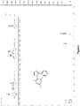
- a green emissive moleculeis tris(2-phenylpyridine) iridium, denoted Ir(ppy) 3 , which has the following structure:
- organicincludes polymeric materials as well as small molecule organic materials that may be used to fabricate organic opto-electronic devices.
- Small moleculerefers to any organic material that is not a polymer, and "small molecules” may actually be quite large. Small molecules may include repeat units in some circumstances. For example, using a long chain alkyl group as a substituent does not remove a molecule from the "small molecule” class. Small molecules may also be incorporated into polymers, for example as a pendent group on a polymer backbone or as a part of the backbone. Small molecules may also serve as the core moiety of a dendrimer, which consists of a series of chemical shells built on the core moiety.
- the core moiety of a dendrimermay be a fluorescent or phosphorescent small molecule emitter.
- a dendrimermay be a "small molecule,” and it is believed that all dendrimers currently used in the field of OLEDs are small molecules.
- topmeans furthest away from the substrate, while “bottom” means closest to the substrate.
- first layeris described as “disposed over” a second layer, the first layer is disposed further away from substrate. There may be other layers between the first and second layer, unless it is specified that the first layer is "in contact with” the second layer.
- a cathodemay be described as “disposed over” an anode, even though there are various organic layers in between.
- solution processablemeans capable of being dissolved, dispersed, or transported in and/or deposited from a liquid medium, either in solution or suspension form.
- a ligandmay be referred to as "photoactive” when it is believed that the ligand directly contributes to the photoactive properties of an emissive material.
- a ligandmay be referred to as "ancillary” when it is believed that the ligand does not contribute to the photoactive properties of an emissive material, although an ancillary ligand may alter the properties of a photoactive ligand.
- a first "Highest Occupied Molecular Orbital” (HOMO) or “Lowest Unoccupied Molecular Orbital” (LUMO) energy levelis “greater than” or "higher than” a second HOMO or LUMO energy level if the first energy level is closer to the vacuum energy level.
- IPionization potentials
- a higher HOMO energy levelcorresponds to an IP having a smaller absolute value (an IP that is less negative).
- a higher LUMO energy levelcorresponds to an electron affinity (EA) having a smaller absolute value (an EA that is less negative).
- the LUMO energy level of a materialis higher than the HOMO energy level of the same material.
- a "higher” HOMO or LUMO energy levelappears closer to the top of such a diagram than a "lower” HOMO or LUMO energy level.
- a first work functionis "greater than” or “higher than” a second work function if the first work function has a higher absolute value. Because work functions are generally measured as negative numbers relative to vacuum level, this means that a "higher” work function is more negative. On a conventional energy level diagram, with the vacuum level at the top, a “higher” work function is illustrated as further away from the vacuum level in the downward direction. Thus, the definitions of HOMO and LUMO energy levels follow a different convention than work functions.
- the present disclosurerelates to a compound having a surface region of highly negative electrostatic potential.
- the compoundcomprises a ligand L A represented by Formula I: wherein the ligand L A is coordinated to a metal M as represented by the dashed lines, and optionally, the metal M is coordinated to one or more ligands L B ;
- An OLEDcomprising the compound of the present disclosure in an organic layer therein is also disclosed.
- a consumer product comprising the OLEDis also disclosed.
- an OLEDcomprises at least one organic layer disposed between and electrically connected to an anode and a cathode.
- the anodeinjects holes and the cathode injects electrons into the organic layer(s).
- the injected holes and electronseach migrate toward the oppositely charged electrode.
- an "exciton”which is a localized electron-hole pair having an excited energy state, is formed.
- Lightis emitted when the exciton relaxes via a photoemissive mechanism.
- the excitonmay be localized on an excimer or an exciplex. Non-radiative mechanisms, such as thermal relaxation, may also occur, but are generally considered undesirable.
- the initial OLEDsused emissive molecules that emitted light from their singlet states ("fluorescence") as disclosed, for example, in U.S. Pat. No. 4,769,292 , which is incorporated by reference in its entirety. Fluorescent emission generally occurs in a time frame of less than 10 nanoseconds.
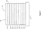
- FIG. 1shows an organic light emitting device 100.
- Device 100may include a substrate 110, an anode 115, a hole injection layer 120, a hole transport layer 125, an electron blocking layer 130, an emissive layer 135, a hole blocking layer 140, an electron transport layer 145, an electron injection layer 150, a protective layer 155, a cathode 160, and a barrier layer 170.
- Cathode 160is a compound cathode having a first conductive layer 162 and a second conductive layer 164.
- Device 100may be fabricated by depositing the layers described, in order. The properties and functions of these various layers, as well as example materials, are described in more detail in US 7,279,704 at cols. 6-10, which are incorporated by reference.
- each of these layersare available.
- a flexible and transparent substrate-anode combinationis disclosed in U.S. Pat. No. 5,844,363 , which is incorporated by reference in its entirety.
- An example of a p-doped hole transport layeris m-MTDATA doped with F 4 -TCNQ at a molar ratio of 50:1, as disclosed in U.S. Patent Application Publication No. 2003/0230980 , which is incorporated by reference in its entirety.
- Examples of emissive and host materialsare disclosed in U.S. Pat. No. 6,303,238 to Thompson et al., which is incorporated by reference in its entirety.
- An example of an n-doped electron transport layeris BPhen doped with Li at a molar ratio of 1:1, as disclosed in U.S. Patent Application Publication No. 2003/0230980 , which is incorporated by reference in its entirety.
- U.S. Pat. Nos. 5,703,436 and 5,707,745which are incorporated by reference in their entireties, disclose examples of cathodes including compound cathodes having a thin layer of metal such as Mg:Ag with an overlying transparent, electrically-conductive, sputter-deposited ITO layer.
- the theory and use of blocking layersis described in more detail in U.S. Pat. No. 6,097,147 and U.S. Patent Application Publication No.
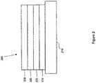
- FIG. 2shows an inverted OLED 200.
- the deviceincludes a substrate 210, a cathode 215, an emissive layer 220, a hole transport layer 225, and an anode 230.
- Device 200may be fabricated by depositing the layers described, in order. Because the most common OLED configuration has a cathode disposed over the anode, and device 200 has cathode 215 disposed under anode 230, device 200 may be referred to as an "inverted" OLED. Materials similar to those described with respect to device 100 may be used in the corresponding layers of device 200.
- FIG. 2provides one example of how some layers may be omitted from the structure of device 100.
- FIGS. 1 and 2The simple layered structure illustrated in FIGS. 1 and 2 is provided by way of non-limiting example, and it is understood that embodiments of the invention may be used in connection with a wide variety of other structures.
- the specific materials and structures describedare exemplary in nature, and other materials and structures may be used.
- Functional OLEDsmay be achieved by combining the various layers described in different ways, or layers may be omitted entirely, based on design, performance, and cost factors. Other layers not specifically described may also be included. Materials other than those specifically described may be used. Although many of the examples provided herein describe various layers as comprising a single material, it is understood that combinations of materials, such as a mixture of host and dopant, or more generally a mixture, may be used. Also, the layers may have various sublayers.
- hole transport layer 225transports holes and injects holes into emissive layer 220, and may be described as a hole transport layer or a hole injection layer.
- an OLEDmay be described as having an "organic layer" disposed between a cathode and an anode. This organic layer may comprise a single layer, or may further comprise multiple layers of different organic materials as described, for example, with respect to FIGS. 1 and 2 .
- OLEDscomprised of polymeric materials (PLEDs) such as disclosed in U.S. Pat. No. 5,247,190 to Friend et al. , which is incorporated by reference in its entirety.
- PLEDspolymeric materials
- OLEDs having a single organic layermay be used.
- OLEDsmay be stacked, for example as described in U.S. Pat. No. 5,707,745 to Forrest et al , which is incorporated by reference in its entirety.
- the OLED structuremay deviate from the simple layered structure illustrated in FIGS. 1 and 2 .
- the substratemay include an angled reflective surface to improve out-coupling, such as a mesa structure as described in U.S. Pat. No. 6,091,195 to Forrest et al. , and/or a pit structure as described in U.S. Pat. No. 5,834,893 to Bulovic et al. , which are incorporated by reference in their entireties.
- any of the layers of the various embodimentsmay be deposited by any suitable method.
- preferred methodsinclude thermal evaporation, ink-jet, such as described in U.S. Pat. Nos. 6,013,982 and 6,087,196 , which are incorporated by reference in their entireties, organic vapor phase deposition (OVPD), such as described in U.S. Pat. No. 6,337,102 to Forrest et al. , which is incorporated by reference in its entirety, and deposition by organic vapor jet printing (OVJP), such as described in U.S. Pat. No. 7,431,968 , which is incorporated by reference in its entirety.
- OVPDorganic vapor phase deposition
- OJPorganic vapor jet printing
- Other suitable deposition methodsinclude spin coating and other solution based processes.
- Solution based processesare preferably carried out in nitrogen or an inert atmosphere.
- preferred methodsinclude thermal evaporation.
- Preferred patterning methodsinclude deposition through a mask, cold welding such as described in U.S. Pat. Nos. 6,294,398 and 6,468,819 , which are incorporated by reference in their entireties, and patterning associated with some of the deposition methods such as ink-jet and organic vapor jet printing (OVJP). Other methods may also be used.
- the materials to be depositedmay be modified to make them compatible with a particular deposition method. For example, substituents such as alkyl and aryl groups, branched or unbranched, and preferably containing at least 3 carbons, may be used in small molecules to enhance their ability to undergo solution processing.
- Substituents having 20 carbons or moremay be used, and 3-20 carbons is a preferred range. Materials with asymmetric structures may have better solution processability than those having symmetric structures, because asymmetric materials may have a lower tendency to recrystallize. Dendrimer substituents may be used to enhance the ability of small molecules to undergo solution processing.
- Devices fabricated in accordance with embodiments of the present inventionmay further optionally comprise a barrier layer.
- a barrier layerOne purpose of the barrier layer is to protect the electrodes and organic layers from damaging exposure to harmful species in the environment including moisture, vapor and/or gases, etc.
- the barrier layermay be deposited over, under or next to a substrate, an electrode, or over any other parts of a device including an edge.
- the barrier layermay comprise a single layer, or multiple layers.
- the barrier layermay be formed by various known chemical vapor deposition techniques and may include compositions having a single phase as well as compositions having multiple phases. Any suitable material or combination of materials may be used for the barrier layer.
- the barrier layermay incorporate an inorganic or an organic compound or both.
- the preferred barrier layercomprises a mixture of a polymeric material and a non-polymeric material as described in U.S. Pat. No. 7,968,146 , PCT Pat. Application Nos. PCT/US2007/023098 and PCT/US2009/042829 , which are herein incorporated by reference in their entireties.
- the aforesaid polymeric and non-polymeric materials comprising the barrier layershould be deposited under the same reaction conditions and/or at the same time.
- the weight ratio of polymeric to non-polymeric materialmay be in the range of 95:5 to 5:95.
- the polymeric material and the non-polymeric materialmay be created from the same precursor material.
- the mixture of a polymeric material and a non-polymeric materialconsists essentially of polymeric silicon and inorganic silicon.
- Devices fabricated in accordance with embodiments of the inventioncan be incorporated into a wide variety of electronic component modules (or units) that can be incorporated into a variety of electronic products or intermediate components. Examples of such electronic products or intermediate components include display screens, lighting devices such as discrete light source devices or lighting panels, etc. that can be utilized by the end-user product manufacturers. Such electronic component modules can optionally include the driving electronics and/or power source(s). Devices fabricated in accordance with embodiments of the invention can be incorporated into a wide variety of consumer products that have one or more of the electronic component modules (or units) incorporated therein.
- a consumer product comprising an OLED that includes the compound of the present disclosure in the organic layer in the OLEDis disclosed.
- Such consumer productswould include any kind of products that include one or more light source(s) and/or one or more of some type of visual displays.
- Some examples of such consumer productsinclude flat panel displays, curved displays, computer monitors, medical monitors, televisions, billboards, lights for interior or exterior illumination and/or signaling, heads-up displays, fully or partially transparent displays, flexible displays, rollable displays, foldable displays, stretchable displays, laser printers, telephones, mobile phones, tablets, phablets, personal digital assistants (PDAs), wearable devices, laptop computers, digital cameras, camcorders, viewfinders, micro-displays (displays that are less than 2 inches diagonal), 3-D displays, virtual reality or augmented reality displays, vehicles, video walls comprising multiple displays tiled together, theater or stadium screen, a light therapy device, and a sign.
- control mechanismsmay be used to control devices fabricated in accordance with the present invention, including passive matrix and active matrix. Many of the devices are intended for use in a temperature range comfortable to humans, such as 18 degrees C. to 30 degrees C., and more preferably at room temperature (20-25 degrees C), but could be used outside this temperature range, for example, from -40 degree C to + 80 degree C.
- the materials and structures described hereinmay have applications in devices other than OLEDs.
- other optoelectronic devicessuch as organic solar cells and organic photodetectors may employ the materials and structures.
- organic devicessuch as organic transistors, may employ the materials and structures.
- halohalogen
- halidehalogen
- fluorinechlorine, bromine, and iodine
- acylrefers to a substituted carbonyl radical (C(O)-R s ).
- estersrefers to a substituted oxycarbonyl (-O-C(O)-R s or -C(O)-O-R s ) radical.
- etherrefers to an -OR s radical.
- sulfanylor "thio-ether” are used interchangeably and refer to a -SR s radical.
- sulfinylrefers to a -S(O)-R s radical.
- sulfonylrefers to a -SO 2 -R s radical.
- phosphinorefers to a -P(R s ) 3 radical, wherein each R s can be same or different.
- silrefers to a -Si(R s ) 3 radical, wherein each R s can be same or different.
- R scan be hydrogen or a substituent selected from the group consisting of deuterium, halogen, alkyl, cycloalkyl, heteroalkyl, heterocycloalkyl, arylalkyl, alkoxy, aryloxy, amino, silyl, alkenyl, cycloalkenyl, heteroalkenyl, alkynyl, aryl, heteroaryl, and combination thereof.
- Preferred R sis selected from the group consisting of alkyl, cycloalkyl, aryl, heteroaryl, and combination thereof.
- alkylrefers to and includes both straight and branched chain alkyl radicals.
- Preferred alkyl groupsare those containing from one to fifteen carbon atoms and includes methyl, ethyl, propyl, 1-methylethyl, butyl, 1-methylpropyl, 2-methylpropyl, pentyl, 1-methylbutyl, 2-methylbutyl, 3-methylbutyl, 1,1-dimethylpropyl, 1,2-dimethylpropyl, 2,2-dimethylpropyl,and the like. Additionally, the alkyl group is optionally substituted.
- cycloalkylrefers to and includes monocyclic, polycyclic, and spiro alkyl radicals.
- Preferred cycloalkyl groupsare those containing 3 to 12 ring carbon atoms and includes cyclopropyl, cyclopentyl, cyclohexyl, bicyclo[3.1. 1]heptyl, spiro[4.5]decyl, spiro[5.5]undecyl, adamantyl, and the like. Additionally, the cycloalkyl group is optionally substituted.
- heteroalkylor “heterocycloalkyl” refer to an alkyl or a cycloalkyl radical, respectively, having at least one carbon atom replaced by a heteroatom.
- the at least one heteroatomis selected from O, S, N, P, B, Si and Se, preferably, O, S or N.
- the heteroalkyl or heterocycloalkyl groupis optionally substituted.
- alkenylrefers to and includes both straight and branched chain alkene radicals.
- Alkenyl groupsare essentially alkyl groups that include at least one carbon-carbon double bond in the alkyl chain.
- Cycloalkenyl groupsare essentially cycloalkyl groups that include at least one carbon-carbon double bond in the cycloalkyl ring.
- heteroalkenylrefers to an alkenyl radical having at least one carbon atom replaced by a heteroatom.
- the at least one heteroatomis selected from O, S, N, P, B, Si, and Se, preferably, O, S, or N.
- Preferred alkenyl, cycloalkenyl, or heteroalkenyl groupsare those containing two to fifteen carbon atoms. Additionally, the alkenyl, cycloalkenyl, or heteroalkenyl group is optionally substituted.
- alkynylrefers to and includes both straight and branched chain alkyne radicals. Preferred alkynyl groups are those containing two to fifteen carbon atoms. Additionally, the alkynyl group is optionally substituted.
- aralkylor “arylalkyl” are used interchangeably and refer to an alkyl group that is substituted with an aryl group. Additionally, the aralkyl group is optionally substituted.
- heterocyclic grouprefers to and includes aromatic and non-aromatic cyclic radicals containing at least one heteroatom.
- the at least one heteroatomis selected from O, S, N, P, B, Si, and Se, preferably, O, S, or N.
- Hetero-aromatic cyclic radicalsmay be used interchangeably with heteroaryl.
- Preferred hetero-non-aromatic cyclic groupsare those containing 3 to 7 ring atoms which includes at least one hetero atom, and includes cyclic amines such as morpholino, piperidino, pyrrolidino, and the like, and cyclic ethers/thio-ethers, such as tetrahydrofuran, tetrahydropyran, tetrahydrothiophene, and the like. Additionally, the heterocyclic group may be optionally substituted.
- arylrefers to and includes both single-ring aromatic hydrocarbyl groups and polycyclic aromatic ring systems.
- the polycyclic ringsmay have two or more rings in which two carbons are common to two adjoining rings (the rings are "fused") wherein at least one of the rings is an aromatic hydrocarbyl group, e.g., the other rings can be cycloalkyls, cycloalkenyls, aryl, heterocycles, and/or heteroaryls.
- Preferred aryl groupsare those containing six to thirty carbon atoms, preferably six to twenty carbon atoms, more preferably six to twelve carbon atoms. Especially preferred is an aryl group having six carbons, ten carbons or twelve carbons.
- Suitable aryl groupsinclude phenyl, biphenyl, triphenyl, triphenylene, tetraphenylene, naphthalene, anthracene, phenalene, phenanthrene, fluorene, pyrene, chrysene, perylene, and azulene, preferably phenyl, biphenyl, triphenyl, triphenylene, fluorene, and naphthalene. Additionally, the aryl group is optionally substituted.
- heteroarylrefers to and includes both single-ring aromatic groups and polycyclic aromatic ring systems that include at least one heteroatom.
- the heteroatomsinclude, but are not limited to O, S, N, P, B, Si, and Se. In many instances, O, S, or N are the preferred heteroatoms.
- Hetero-single ring aromatic systemsare preferably single rings with 5 or 6 ring atoms, and the ring can have from one to six heteroatoms.
- the hetero-polycyclic ring systemscan have two or more rings in which two atoms are common to two adjoining rings (the rings are "fused") wherein at least one of the rings is a heteroaryl, e.g., the other rings can be cycloalkyls, cycloalkenyls, aryl, heterocycles, and/or heteroaryls.
- the hetero-polycyclic aromatic ring systemscan have from one to six heteroatoms per ring of the polycyclic aromatic ring system.
- Preferred heteroaryl groupsare those containing three to thirty carbon atoms, preferably three to twenty carbon atoms, more preferably three to twelve carbon atoms.
- Suitable heteroaryl groupsinclude dibenzothiophene, dibenzofuran, dibenzoselenophene, furan, thiophene, benzofuran, benzothiophene, benzoselenophene, carbazole, indolocarbazole, pyridylindole, pyrrolodipyridine, pyrazole, imidazole, triazole, oxazole, thiazole, oxadiazole, oxatriazole, dioxazole, thiadiazole, pyridine, pyridazine, pyrimidine, pyrazine, triazine, oxazine, oxathiazine, oxadiazine, indole, benzimidazole, indazole, indoxazine, benzoxazole, benzisoxazole, benzothiazole, quinoline, isoquinoline, cinnoline, qui
- aryl and heteroaryl groups listed abovethe groups of triphenylene, naphthalene, anthracene, dibenzothiophene, dibenzofuran, dibenzoselenophene, carbazole, indolocarbazole, imidazole, pyridine, pyrazine, pyrimidine, triazine, and benzimidazole, and the respective aza-analogs of each thereof are of particular interest.
- alkyl, cycloalkyl, heteroalkyl, heterocycloalkyl, alkenyl, cycloalkenyl, heteroalkenyl, alkynyl, aralkyl, heterocyclic group, aryl, and heteroaryl, as used herein,are independently unsubstituted, or independently substituted, with one or more general substituents.
- the general substituentsare selected from the group consisting of deuterium, halogen, alkyl, cycloalkyl, heteroalkyl, heterocycloalkyl, arylalkyl, alkoxy, aryloxy, amino, silyl, alkenyl, cycloalkenyl, heteroalkenyl, alkynyl, aryl, heteroaryl, acyl, carboxylic acid, ether, ester, nitrile, isonitrile, sulfanyl, sulfinyl, sulfonyl, phosphino, and combinations thereof.
- the preferred general substituentsare selected from the group consisting of deuterium, fluorine, alkyl, cycloalkyl, heteroalkyl, alkoxy, aryloxy, amino, silyl, alkenyl, cycloalkenyl, heteroalkenyl, aryl, heteroaryl, nitrile, isonitrile, sulfanyl, and combinations thereof.
- the preferred general substituentsare selected from the group consisting of deuterium, fluorine, alkyl, cycloalkyl, alkoxy, aryloxy, amino, silyl, aryl, heteroaryl, sulfanyl, and combinations thereof.
- the more preferred general substituentsare selected from the group consisting of deuterium, fluorine, alkyl, cycloalkyl, aryl, heteroaryl, and combinations thereof.
- substituted and substitutionrefer to a substituent other than H that is bonded to the relevant position, e.g., a carbon or nitrogen.
- R 1when R 1 represents monosubstitution, then one R 1 must be other than H (i.e., a substitution). Similarly, when R 1 represents disubstitution, then two of R 1 must be other than H.
- R 1when R 1 represents no substitution, R 1 , for example, can be a hydrogen for available valencies of ring atoms, as in carbon atoms for benzene and the nitrogen atom in pyrrole, or simply represents nothing for ring atoms with fully filled valencies, e.g., the nitrogen atom in pyridine.
- the maximum number of substitutions possible in a ring structurewill depend on the total number of available valencies in the ring atoms.
- substitutionincludes a combination of two to four of the listed groups.
- substitutionincludes a combination of two to three groups.
- substitutionincludes a combination of two groups.
- Preferred combinations of substituent groupsare those that contain up to fifty atoms that are not hydrogen or deuterium, or those which include up to forty atoms that are not hydrogen or deuterium, or those that include up to thirty atoms that are not hydrogen or deuterium. In many instances, a preferred combination of substituent groups will include up to twenty atoms that are not hydrogen or deuterium.
- aza-dibenzofurani.e. aza-dibenzofuran, aza-dibenzothiophene, etc.
- azatriphenyleneencompasses both dibenzo[ f,h ]quinoxaline and dibenzo[ f,h ]quinoline.
- deuteriumrefers to an isotope of hydrogen.
- Deuterated compoundscan be readily prepared using methods known in the art. For example, U.S. Pat. No. 8,557,400 , Patent Pub. No. WO 2006/095951 , and U.S. Pat. Application Pub. No. US 2011/0037057 , which are hereby incorporated by reference in their entireties, describe the making of deuterium-substituted organometallic complexes. Further reference is made to Ming Yan, et al., Tetrahedron 2015, 71, 1425-30 and Atzrodt et al., Angew. Chem. Int. Ed. (Reviews) 2007, 46, 7744-65 , which are incorporated by reference in their entireties, describe the deuteration of the methylene hydrogens in benzyl amines and efficient pathways to replace aromatic ring hydrogens with deuterium, respectively.
- a pair of adjacent substituentscan be optionally joined or fused into a ring.
- the preferred ringis a five, six, or seven-membered carbocyclic or heterocyclic ring, includes both instances where the portion of the ring formed by the pair of substituents is saturated and where the portion of the ring formed by the pair of substituents is unsaturated.
- "adjacent"means that the two substituents involved can be on the same ring next to each other, or on two neighboring rings having the two closest available substitutable positions, such as 2, 2' positions in a biphenyl, or 1, 8 position in a naphthalene, as long as they can form a stable fused ring system.
- the present disclosurerelates to a compound having a surface region of highly negative electrostatic potential.
- the compoundcomprises a ligand L A represented by Formula I: wherein the ligand L A is coordinated to a metal M as represented by the dashed lines, and optionally, the metal M is coordinated to one or more ligands L B ;
- Y 2represents CR 2 , wherein R 2 is perfluoroalkyl or perfluoroaryl.
- Y 1 and Y 3each represent CR 2 , wherein R 2 is perfluoroalkyl or perfluoroaryl.
- Y 1 , Y 2 , and Y 3each represent CR 2 , wherein R 2 is perfluoroalkyl or perfluoroaryl.
- at least one of Y 3 , Y 4 , and Y 5represents CR 2 , wherein R 2 is trifluromethyl, pentafluoroethyl, or pentafluorophenyl.
- the compoundhas the formula M(L A ) x (L B ) y , where x is 1, 2, or 3; y is 0, 1, or 2; and x + y is the oxidation state of the metal.
- the optional ligand L Bis bidentate.
- the optional ligand L Bis monoanionic.
- each of the ligands L Acan be the same as, or different from, each other ligand L A .
- each of the ligands L Bcan be the same as, or different from, each other ligand L B .
- the ligand L Ahas a different structure from the ligand L B .
- the ligand L Bdoes not include a perfluoroalkyl or perfluoroaryl group.
- the metal Mis selected from the group consisting of Re, Os, Rh, Ir, Pd, Pt, Ag, Ag, and Cu.
- the metal Mis selected from Os, Ru, Ir, or Rh.
- the ligand L Ais bidentate, and the coordination to the metal includes one, two, or three ligand(s) L A of the Formulae I, or one of the select ligands L A infra.
- the metal Mis also coordinated with one or more additional ligand L B .
- the metal Mis selected from Pt or Pd.
- the coordination to the metalincludes one or two ligand(s) L A of Formulae I, or one or two of the select ligands infra. In one embodiment, if there are two ligands L A , the ligands L A can be the same or different. In one embodiment, one ligand L A is linked to the same or different ligand L A or to a ligand L B to form a tetradentate ligand. In one embodiment, the compound comprises one ligand L A and one optional ligand L B . In one embodiment, the ligand L A is linked to the ligand L B through any substituent to form a tetradentate ligand.
- the compoundhas the formula Ir(L A ) 3 . In one embodiment, the compound having the formula Ir(L A ) 3 is the facial ( fac ) isomer. In one embodiment, the compound has a neutral charge.
- the compoundcomprises a surface region of high electrostatic potential (ESP).
- the region of high ESPcomprises a region of very negative ESP.
- the ESP of the compoundis non-uniform.
- the most negative ESPs of the compoundare symmetrically disposed around the C 3 axis.
- the negative ESP of the compoundforms a patch of high ESP.
- the patch of high ESPreinforces an alignment of the molecule that favors a low anisotropy factor.
- the patch of high ESPhas a lower affinity for the surface of the host matrix.
- the lower affinity of the region of high ESPis caused by a decrease in van der Waals interactions.
- the region of high ESPreinforces horizontal alignment during deposition of the compound.
- ring Ais a heteroaryl ring selected from the group of pyridine, imidazole, pyrrole, and N-heterocyclic carbene, wherein ring A is optionally further substituted with one or more groups R 1 . In one embodiment, two groups R 1 join to form a fused aryl or heteroaryl ring.
- X 3is C, X 2 is N, and ring A is a heteroaromatic ring. In one embodiment, X 3 is C, X 2 is C, and ring A is an N-heterocyclic carbene.
- the ligand L Ais represented by one of the following structures: wherein Y 5 to Y 12 each independently represent C or N;
- the ligand L Ais represented by one of the following structures:
- a formulationcomprising the compound described herein is also disclosed.
- the present disclosurerelates to an organic electroluminescent device (OLED) comprising an anode; a cathode; and an organic layer, disposed between the anode and the cathode, comprising a compound of the present disclosure.
- OLEDorganic electroluminescent device
- the OLEDhas one or more characteristics selected from the group consisting of being flexible, being rollable, being foldable, being stretchable, and being curved. In some embodiments, the OLED is transparent or semi-transparent. In some embodiments, the OLED further comprises a layer comprising carbon nanotubes.
- the OLEDfurther comprises a layer comprising a delayed fluorescent emitter.
- the OLEDcomprises a RGB pixel arrangement or white plus color filter pixel arrangement.
- the OLEDis a mobile device, a hand held device, or a wearable device.
- the OLEDis a display panel having less than 10 inch diagonal or 50 square inch area.
- the OLEDis a display panel having at least 10 inch diagonal or 50 square inch area.
- the OLEDis a lighting panel.
- the compoundcan be an emissive dopant.
- the compoundcan produce emissions via phosphorescence, fluorescence, thermally activated delayed fluorescence, i.e., TADF (also referred to as E-type delayed fluorescence; see, e.g., U.S. Application No. 15/700,352 , which is hereby incorporated by reference in its entirety), triplet-triplet annihilation, or combinations of these processes.
- the emissive dopantcan be a racemic mixture, or can be enriched in one enantiomer.
- the compoundis neutrally charged.
- the compoundcan be homoleptic (each ligand is the same).
- the compoundcan be heteroleptic (at least one ligand is different from others).
- the ligandscan all be the same in some embodiments.
- at least one ligandis different from the other ligands.
- every ligandcan be different from each other. This is also true in embodiments where a ligand being coordinated to a metal can be linked with other ligands being coordinated to that metal to form a tridentate, tetradentate, pentadentate, or hexadentate ligands.
- the coordinating ligandsare being linked together, all of the ligands can be the same in some embodiments, and at least one of the ligands being linked can be different from the other ligand(s) in some other embodiments.
- the compoundcan be used as a phosphorescent sensitizer in an OLED where one or multiple layers in the OLED contains an acceptor in the form of one or more fluorescent and/or delayed fluorescence emitters.
- the compoundcan be used as one component of an exciplex to be used as a sensitizer.
- the compoundmust be capable of energy transfer to the acceptor and the acceptor will emit the energy or further transfer energy to a final emitter.
- the acceptor concentrationscan range from 0.001% to 100%.
- the acceptorcould be in either the same layer as the phosphorescent sensitizer or in one or more different layers.
- the acceptoris a TADF emitter.
- the acceptoris a fluorescent emitter.
- the emissioncan arise from any or all of the sensitizer, acceptor, and final emitter.
- the OLED disclosed hereincan be incorporated into one or more of a consumer product, an electronic component module, and a lighting panel.
- the organic layercan be an emissive layer and the compound can be an emissive dopant in some embodiments, while the compound can be a non-emissive dopant in other embodiments.
- the organic layercan also include a host.
- a hostIn some embodiments, two or more hosts are preferred.
- the hosts usedmaybe a) bipolar, b) electron transporting, c) hole transporting or d) wide band gap materials that play little role in charge transport.
- the hostcan include a metal complex.
- the hostcan be a triphenylene containing benzo-fused thiophene or benzo-fused furan.
- ncan range from 1 to 10; and Ar 1 and Ar 2 can be independently selected from the group consisting of benzene, biphenyl, naphthalene, triphenylene, carbazole, and heteroaromatic analogs thereof.
- the hostcan be an inorganic compound.
- a Zn containing inorganic materiale.g. ZnS.
- the hostcan be a compound comprising at least one chemical group selected from the group consisting of triphenylene, carbazole, dibenzothiophene, dibenzofuran, dibenzoselenophene, azatriphenylene, azacarbazole, aza-dibenzothiophene, aza-dibenzofuran, and aza-dibenzoselenophene.
- the hostcan include a metal complex.
- the hostcan be, but is not limited to, a specific compound selected from the group consisting of: , and combinations thereof. Additional information on possible hosts is provided below.
- a formulation that comprises the novel compound disclosed hereinis described.
- the formulationcan include one or more components selected from the group consisting of a solvent, a host, a hole injection material, hole transport material, electron blocking material, hole blocking material, and an electron transport material, disclosed herein.
- the present disclosureencompasses any chemical structure comprising the novel compound of the present disclosure, or a monovalent or polyvalent variant thereof.
- the inventive compound, or a monovalent or polyvalent variant thereofcan be a part of a larger chemical structure.
- Such chemical structurecan be selected from the group consisting of a monomer, a polymer, a macromolecule, and a supramolecule (also known as supermolecule).
- a "monovalent variant of a compound”refers to a moiety that is identical to the compound except that one hydrogen has been removed and replaced with a bond to the rest of the chemical structure.
- a "polyvalent variant of a compound”refers to a moiety that is identical to the compound except that more than one hydrogen has been removed and replaced with a bond or bonds to the rest of the chemical structure.
- the inventive compoundcan also be incorporated into the supramolecule complex without covalent bonds.
- emissive dopants disclosed hereinmay be used in conjunction with a wide variety of hosts, transport layers, blocking layers, injection layers, electrodes and other layers that may be present.
- the materials described or referred to beloware non-limiting examples of materials that may be useful in combination with the compounds disclosed herein, and one of skill in the art can readily consult the literature to identify other materials that may be useful in combination.
- a charge transport layercan be doped with conductivity dopants to substantially alter its density of charge carriers, which will in turn alter its conductivity.
- the conductivityis increased by generating charge carriers in the matrix material, and depending on the type of dopant, a change in the Fermi level of the semiconductor may also be achieved.
- Hole-transporting layercan be doped by p-type conductivity dopants and n-type conductivity dopants are used in the electron-transporting layer.
- Non-limiting examples of the conductivity dopants that may be used in an OLED in combination with materials disclosed hereinare exemplified below together with references that disclose those materials: EP01617493 , EP01968131 , EP2020694 , EP2684932 , US20050139810 , US20070160905 , US20090167167 , US2010288362 , WO06081780 , WO2009003455 , WO2009008277 , WO2009011327 , WO2014009310 , US2007252140 , US2015060804 , US20150123047 , and US2012146012 .
- a hole injecting/transporting material to be used in the present inventionis not particularly limited, and any compound may be used as long as the compound is typically used as a hole injecting/transporting material.
- the materialinclude, but are not limited to: a phthalocyanine or porphyrin derivative; an aromatic amine derivative; an indolocarbazole derivative; a polymer containing fluorohydrocarbon; a polymer with conductivity dopants; a conducting polymer, such as PEDOT/PSS; a self-assembly monomer derived from compounds such as phosphonic acid and silane derivatives; a metal oxide derivative, such as MoO x ; a p-type semiconducting organic compound, such as 1,4,5,8,9,12-Hexaazatriphenylenehexacarbonitrile; a metal complex, and a crosslinkable compounds.
- aromatic amine derivatives used in HIL or HTLinclude, but not limit to the following general structures:
- Each of Ar 1 to Ar 9is selected from the group consisting of aromatic hydrocarbon cyclic compounds such as benzene, biphenyl, triphenyl, triphenylene, naphthalene, anthracene, phenalene, phenanthrene, fluorene, pyrene, chrysene, perylene, and azulene; the group consisting of aromatic heterocyclic compounds such as dibenzothiophene, dibenzofuran, dibenzoselenophene, furan, thiophene, benzofuran, benzothiophene, benzoselenophene, carbazole, indolocarbazole, pyridylindole, pyrrolodipyridine, pyrazole, imidazole, triazole, oxazole, thiazole, oxadiazole, oxatriazole, dioxazole, thiadiazole, pyridine, pyridazine
- Each Armay be unsubstituted or may be substituted by a substituent selected from the group consisting of deuterium, halogen, alkyl, cycloalkyl, heteroalkyl, heterocycloalkyl, arylalkyl, alkoxy, aryloxy, amino, silyl, alkenyl, cycloalkenyl, heteroalkenyl, alkynyl, aryl, heteroaryl, acyl, carboxylic acids, ether, ester, nitrile, isonitrile, sulfanyl, sulfinyl, sulfonyl, phosphino, and combinations thereof.
- a substituentselected from the group consisting of deuterium, halogen, alkyl, cycloalkyl, heteroalkyl, heterocycloalkyl, arylalkyl, alkoxy, aryloxy, amino, silyl, alkenyl, cycloalkenyl, heteroalkeny
- Ar 1 to Ar 9is independently selected from the group consisting of: wherein k is an integer from 1 to 20; X 101 to X 108 is C (including CH) or N; Z 101 is NAr 1 , O, or S; Ar 1 has the same group defined above.
- metal complexes used in HIL or HTLinclude, but are not limited to the following general formula: wherein Met is a metal, which can have an atomic weight greater than 40; (Y 101 -Y 102 ) is a bidentate ligand, Y 101 and Y 102 are independently selected from C, N, O, P, and S; L 101 is an ancillary ligand; k' is an integer value from 1 to the maximum number of ligands that may be attached to the metal; and k'+k" is the maximum number of ligands that may be attached to the metal.
- (Y 101 -Y 102 )is a 2-phenylpyridine derivative. In another aspect, (Y 101 -Y 102 ) is a carbene ligand. In another aspect, Met is selected from Ir, Pt, Os, and Zn. In a further aspect, the metal complex has a smallest oxidation potential in solution vs. Fc + /Fc couple less than about 0.6 V.
- Non-limiting examples of the HIL and HTL materials that may be used in an OLED in combination with materials disclosed hereinare exemplified below together with references that disclose those materials: CN102702075 , DE102012005215 , EP01624500 , EP01698613 , EP01806334 , EP01930964 , EP01972613 , EP01997799 , EP02011790 , EP02055700 , EP02055701 , EP1725079 , EP2085382 , EP2660300 , EP650955 , JP07-073529 , JP2005112765 , JP2007091719 , JP2008021687 , JP2014-009196 , KR20110088898 , KR20130077473 , TW201139402 , US06517957 , US20020158242 , US20030162053 , US20050123751 , US20060182993 , US200602402
- An electron blocking layermay be used to reduce the number of electrons and/or excitons that leave the emissive layer.
- the presence of such a blocking layer in a devicemay result in substantially higher efficiencies, and/or longer lifetime, as compared to a similar device lacking a blocking layer.
- a blocking layermay be used to confine emission to a desired region of an OLED.
- the EBL materialhas a higher LUMO (closer to the vacuum level) and/or higher triplet energy than the emitter closest to the EBL interface.
- the EBL materialhas a higher LUMO (closer to the vacuum level) and/or higher triplet energy than one or more of the hosts closest to the EBL interface.
- the compound used in EBLcontains the same molecule or the same functional groups used as one of the hosts described below.
- the light emitting layer of the organic EL device of the present inventionpreferably contains at least a metal complex as light emitting material, and may contain a host material using the metal complex as a dopant material.
- the host materialare not particularly limited, and any metal complexes or organic compounds may be used as long as the triplet energy of the host is larger than that of the dopant. Any host material may be used with any dopant so long as the triplet criteria is satisfied.
- Examples of metal complexes used as hostare preferred to have the following general formula: wherein Met is a metal; (Y 103 -Y 104 ) is a bidentate ligand, Y 103 and Y 104 are independently selected from C, N, O, P, and S; L 101 is an another ligand; k' is an integer value from 1 to the maximum number of ligands that may be attached to the metal; and k'+k" is the maximum number of ligands that may be attached to the metal.
- the metal complexesare: wherein (O-N) is a bidentate ligand, having metal coordinated to atoms O and N.
- Metis selected from Ir and Pt.
- (Y 103 -Y 104 )is a carbene ligand.
- the host compoundcontains at least one of the following groups selected from the group consisting of aromatic hydrocarbon cyclic compounds such as benzene, biphenyl, triphenyl, triphenylene, tetraphenylene, naphthalene, anthracene, phenalene, phenanthrene, fluorene, pyrene, chrysene, perylene, and azulene; the group consisting of aromatic heterocyclic compounds such as dibenzothiophene, dibenzofuran, dibenzoselenophene, furan, thiophene, benzofuran, benzothiophene, benzoselenophene, carbazole, indolocarbazole, pyridylindole, pyrrolodipyridine, pyrazole, imidazole, triazole, oxazole, thiazole, oxadiazole, oxatriazole, dioxazole, thiadia
- Each option within each groupmay be unsubstituted or may be substituted by a substituent selected from the group consisting of deuterium, halogen, alkyl, cycloalkyl, heteroalkyl, heterocycloalkyl, arylalkyl, alkoxy, aryloxy, amino, silyl, alkenyl, cycloalkenyl, heteroalkenyl, alkynyl, aryl, heteroaryl, acyl, carboxylic acids, ether, ester, nitrile, isonitrile, sulfanyl, sulfinyl, sulfonyl, phosphino, and combinations thereof.
- the host compoundcontains at least one of the following groups in the molecule: and wherein R 101 is selected from the group consisting of hydrogen, deuterium, halogen, alkyl, cycloalkyl, heteroalkyl, heterocycloalkyl, arylalkyl, alkoxy, aryloxy, amino, silyl, alkenyl, cycloalkenyl, heteroalkenyl, alkynyl, aryl, heteroaryl, acyl, carboxylic acids, ether, ester, nitrile, isonitrile, sulfanyl, sulfinyl, sulfonyl, phosphino, and combinations thereof, and when it is aryl or heteroaryl, it has the similar definition as Ar's mentioned above.
- kis an integer from 0 to 20 or 1 to 20.
- X 101 to X 108are independently selected from C (including CH) or N.
- Z 101 and Z 102are independently selected from NR 101
- Non-limiting examples of the host materials that may be used in an OLED in combination with materials disclosed hereinare exemplified below together with references that disclose those materials: EP2034538 , EP2034538A , EP2757608 , JP2007254297 , KR20100079458 , KR20120088644 , KR20120129733 , KR20130115564 , TW201329200 , US20030175553 , US20050238919 , US20060280965 , US20090017330 , US20090030202 , US20090167162 , US20090302743 , US20090309488 , US20100012931 , US20100084966 , US20100187984 , US2010187984 , US2012075273 , US2012126221 , US2013009543 , US2013105787 , US2013175519 , US2014001446 , US20140183503 , US20140225088 ,
- One or more additional emitter dopantsmay be used in conjunction with the compound of the present disclosure.
- the additional emitter dopantsare not particularly limited, and any compounds may be used as long as the compounds are typically used as emitter materials.
- suitable emitter materialsinclude, but are not limited to, compounds which can produce emissions via phosphorescence, fluorescence, thermally activated delayed fluorescence, i.e., TADF (also referred to as E-type delayed fluorescence), triplet-triplet annihilation, or combinations of these processes.
- Non-limiting examples of the emitter materials that may be used in an OLED in combination with materials disclosed hereinare exemplified below together with references that disclose those materials: CN103694277 , CN1696137 , EB01238981 , EP01239526 , EP01961743 , EP1239526 , EP1244155 , EP1642951 , EP1647554 , EP1841834 , EP1841834B , EP2062907 , EP2730583 , JP2012074444 , JP2013110263 , JP4478555 , KR1020090133652 , KR20120032054 , KR20130043460 , TW201332980 , US06699599 , US06916554 , US20010019782 , US20020034656 , US20030068526 , US20030072964 , US20030138657 , US20050123788 , US20050244673 , US200512379
- a hole blocking layermay be used to reduce the number of holes and/or excitons that leave the emissive layer.
- the presence of such a blocking layer in a devicemay result in substantially higher efficiencies and/or longer lifetime as compared to a similar device lacking a blocking layer.
- a blocking layermay be used to confine emission to a desired region of an OLED.
- the HBL materialhas a lower HOMO (further from the vacuum level) and/or higher triplet energy than the emitter closest to the HBL interface.
- the HBL materialhas a lower HOMO (further from the vacuum level) and/or higher triplet energy than one or more of the hosts closest to the HBL interface.
- compound used in HBLcontains the same molecule or the same functional groups used as host described above.
- compound used in HBLcontains at least one of the following groups in the molecule: wherein k is an integer from 1 to 20; L 101 is an another ligand, k' is an integer from 1 to 3.
- Electron transport layermay include a material capable of transporting electrons. Electron transport layer may be intrinsic (undoped), or doped. Doping may be used to enhance conductivity. Examples of the ETL material are not particularly limited, and any metal complexes or organic compounds may be used as long as they are typically used to transport electrons.
- compound used in ETLcontains at least one of the following groups in the molecule: wherein R 101 is selected from the group consisting of hydrogen, deuterium, halogen, alkyl, cycloalkyl, heteroalkyl, heterocycloalkyl, arylalkyl, alkoxy, aryloxy, amino, silyl, alkenyl, cycloalkenyl, heteroalkenyl, alkynyl, aryl, heteroaryl, acyl, carboxylic acids, ether, ester, nitrile, isonitrile, sulfanyl, sulfinyl, sulfonyl, phosphino, and combinations thereof, when it is aryl or heteroaryl, it has the similar definition as Ar's mentioned above.
- Ar 1 to Ar 3has the similar definition as Ar's mentioned above.
- kis an integer from 1 to 20.
- X 101 to X 108is selected from C (including CH) or N.
- the metal complexes used in ETLcontains, but not limit to the following general formula: wherein (O-N) or (N-N) is a bidentate ligand, having metal coordinated to atoms O, N or N, N; L 101 is another ligand; k' is an integer value from 1 to the maximum number of ligands that may be attached to the metal.
- Non-limiting examples of the ETL materials that may be used in an OLED in combination with materials disclosed hereinare exemplified below together with references that disclose those materials: CN103508940 , EP01602648 , EP01734038 , EP01956007 , JP2004-022334 , JP2005149918 , JP2005-268199 , KR0117693 , KR20130108183 , US20040036077 , US20070104977 , US2007018155 , US20090101870 , US20090115316 , US20090140637 , US20090179554 , US2009218940 , US2010108990 , US2011156017 , US2011210320 , US2012193612 , US2012214993 , US2014014925 , US2014014927 , US20140284580 , US6656612 , US8415031 , WO2003060956 , WO2007111263 , WO
- the CGLplays an essential role in the performance, which is composed of an n-doped layer and a p-doped layer for injection of electrons and holes, respectively. Electrons and holes are supplied from the CGL and electrodes. The consumed electrons and holes in the CGL are refilled by the electrons and holes injected from the cathode and anode, respectively; then, the bipolar currents reach a steady state gradually.
- Typical CGL materialsinclude n and p conductivity dopants used in the transport layers.
- the hydrogen atomscan be partially or fully deuterated.
- any specifically listed substituentsuch as, without limitation, methyl, phenyl, pyridyl, etc. may be undeuterated, partially deuterated, and fully deuterated versions thereof.
- classes of substituentssuch as, without limitation, alkyl, aryl, cycloalkyl, heteroaryl, etc. also may be undeuterated, partially deuterated, and fully deuterated versions thereof.
- the orientation of facial (fac) tris -cyclometalated iridium complexes in doped films prepared by vacuum depositionis investigated by altering the physical shape and electronic asymmetry in the molecular structure.
- Angle-dependent photoluminescence spectroscopy and Fourier-plane imaging microscopyshow that the orientation of roughly spherical fac-tris(2- phenylpyridyl)iridium (Ir(ppy) 3 ) is isotropic, whereas complexes that are oblate spheroids, fac -tris(mesityl-2-phenyl-1H-imidazole)iridium (Ir(mi) 3 ) and fac -tris((3,5-dimethyl-[1,1'-biphenyl]-4-yl)-2-phenyl-1H-imidazole)iridium (Ir(mip) 3 ), have a net horizontal alignment of their transition dipole moments.
- Optical anisotropy factors of 0.26 and 0.15, respectively,are obtained from the latter complexes when doped into tris (4-(9H-carbazol-9-yl)phenyl)amine host thin films.
- the horizontal alignmentis attributed to the favorable van der Waals interaction between the oblate Ir complexes and host material.
- Trifluoromethyl groups substituted on one polar face of the Ir(ppy) 3 and Ir(mi) 3 complexesintroduce chemical asymmetries in the molecules at the expense of their oblate shapes.
- the anisotropy factors of films doped with these substituted derivativesare lower relative to the parent complexes, indicating that the fluorinated patches reinforce horizontal alignment during deposition.
- High efficiencies obtained from organic light emitting diodes prepared using the Ir dopantsis attributed, in part, to improved outcoupling of electroluminescence brought about by molecular alignment.
- OLEDsOrganic light emitting diodes
- G. Hong, et al., Adv. Mater. 2021, 33Even though 100% internal quantum efficiency has been achieved using phosphorescent dopants, fabrication of extremely high efficiency OLEDs has been hampered by relatively inefficient light extraction from the device ( W. Brütting, et al., physica status solidi (a) 2013, 210, 44 ; Y. Watanabe, et al., Bull. Chem. Soc. Jpn. 2019, 92, 716 ). Typically, 80% of photons produced by the OLED are lost due to waveguiding, absorption and coupling to surface plasmon modes ( N.
- the losses of the light generated by electroluminescencedrop to ca. 30%.
- the outcouplingcan be further improved by controlling alignment of transition dipole moments (TDMs) of the emitting molecules in emissive layer.
- TDMstransition dipole moments
- ⁇p z 2 p x 2 + p y 2 + p z 2 .
- Bis -cyclometalated Ir diketonate complexesare common emissive dopants in OLEDs that show anisotropy factors of 0.22-0.25 in vacuum deposited films, indicating a net in-plane TDM alignment ( C. K. Moon, et al., Nature Communications 2017, 8 ; T. Lee, et al., Nano Lett. 2017, 17, 6464 ).
- C ⁇ Noctahedral (C ⁇ N) 2 Ir(L ⁇ X) type complexes
- Jurow et al.proposed that the organic/vacuum interface induces reorientation of dopants due to the inherent chemical asymmetries of the surface.
- C ⁇ Nrepresents a cyclometalated ligand and L ⁇ X an auxiliary ligand ( M. J. Jurow, et al., Nature Materials 2016, 15, 85 ).
- Ir(ppy) 3 , Ir(ppyCF 3 ) 3 Ir(mi) 3were prepared according to the literature procedure ( A. B. Tamayo, et al., Journal of the American Chemical Society 2003, 125, 7377 ; A. Singh, et al., J. Organomet. Chem. 2015, 776, 51 ; K. Udagawa, et al., Adv. Mater. 2014, 26, 5062 ; J. Y. Zhuang, et al., New J. Chem. 2015, 39, 246 ). Except for Ir(mipp) 3 , three compounds sublime with the reasonable yields (>50%), allowing for them to be employed in OLEDs.
- the reactionwas cooled to ambient temperature and concentrated in vacuo to remove the methanol solvent.
- the crude mixturewas diluted with ethyl acetate and treated with 1 M aqueous sodium hydroxide solution. The layers were then extracted and separated with water three times, and the resultant organic layer was then washed with brine, dried with sodium sulfate and concentrated in vacuo.
- the crude mixturewas further purified by column chromatography (4:1 hexanes:ethyl acetate) to yield a pale yellow solid (1.67 g, 8.6%).
- Phosphoric acid(1.22 g, 12.5 mmol) was added after one hour and the reaction was left to reflux for an additional 24 hrs. The reaction was cooled to ambient temperature and concentrated in vacuo to remove the methanol solvent. The crude mixture was diluted with ethyl acetate and treated with 1 M aqueous sodium hydroxide solution. The layers were then extracted and separated with water three times, and the resultant organic layer was then washed with brine, dried with sodium sulfate and concentrated in vacuo.
- the crude mixturewas diluted with ethyl acetate and extracted with water three times, and the resultant organic layer was then washed with brine, dried with sodium sulfate and concentrated in vacuo.
- the crude mixturewas further purified by column chromatography (4:1 hexanes:ethyl acetate) to yield a pale yellow solid (1.1 g, 36 %).
- Figure 8provides a 1 H NMR spectrum of mipp-H in Acetone-d 6 .
- Figure 10provides a 13 C NMR spectrum of Ir(mip) 3 in Acetone-d 6 : 13 C NMR (101 MHz, acetone) ⁇ 205.16, 156.43, 141.89, 139.85, 136.77, 136.41, 135.93, 131.95, 128.90, 127.78, 127.03, 126.98, 125.91, 120.30, 120.24, 17.21, 17.09.
- Figure 11provides a 13 C NMR spectrum of Ir(miF) 3 in Acetone-d 6 : 13 C NMR (101 MHz, acetone) ⁇ 159.43, 140.09, 139.77, 135.67, 135.24, 133.35, 129.51, 129.41, 126.29, 121.61, 120.36, 115.91, 115.87, 20.27, 16.81, 16.42.
- Figure 12provides a 13 C NMR spectrum of Ir(mipp) 3 in Acetone-d 6 : 13 C NMR (101 MHz, acetone) ⁇ 205.17, 160.48, 156.53, 141.29, 140.41, 140.28, 138.74, 137.46, 136.84, 136.48, 136.32, 136.01, 128.90, 127.53, 127.47, 127.38, 126.91, 126.76, 125.96, 120.69, 120.03, 118.27, 17.25, 17.13.
- Figure 13provides a 13 C NMR spectrum of mip-H in Acetone-d 6 : 13 C NMR (101 MHz, acetone) ⁇ 141.44, 139.82, 135.96, 129.48, 128.87, 128.24, 128.03, 127.72, 127.01, 126.90, 126.55, 122.00, 17.01.
- Figure 14provides a 13 C NMR spectrum of miF-H in Acetone-d 6 : 13 C NMR (101 MHz, acetone) ⁇ 139.14, 134.97, 129.85, 129.42, 126.72, 125.25, 125.21, 125.17, 125.14, 123.14, 20.18, 16.66.
- Figure 15provides a 13 C NMR spectrum of mipp-H in Acetone-d 6 : 13 C NMR (101 MHz, acetone) ⁇ 205.18, 205.18, 205.16, 140.82, 140.32, 140.25, 138.70, 136.83, 136.02, 131.30, 129.48, 128.89, 128.24, 128.03, 127.48, 127.37, 127.32, 126.87, 126.74, 126.54, 122.00, 17.03.
- Figure 16provides a 13 C NMR spectrum of 1-(4-bromo-2,6-dimethylphenyl)-2-phenyl-1 ⁇ 4 ,3 ⁇ 2 -imidazole in Acetone-d 6 : 13 C NMR (101 MHz, acetone) ⁇ 138.11, 136.78, 131.30, 130.98, 129.64, 128.31, 128.21, 126.58, 122.03, 121.80, 16.64.
- Photophysical MeasurementsPhotoluminescence spectra were measured using a QuantaMaster Photon Technology International phosphorescence/fluorescence spectrofluorometer. Phosphorescent lifetimes were measured by time-correlated single-photon counting using an IBH Fluorocube instrument equipped with an LED excitation source. Quantum yield measurements were carried out using a Hamamatsu C9920 system equipped with a xenon lamp, calibrated integrating sphere and model C10027 photonic multi-channel analyzer (PMA). UV-vis spectra were recorded on a Hewlett-Packard 4853 diode array spectrometer. The samples were deaerated by extensive sparging with N 2 .
- PMAphotonic multi-channel analyzer
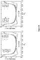
- Table 1Absorption data for the Ir complexes Ir(mi) 3 (1), Ir(miF) 3 (2), and Ir(mip) 3 (3) ⁇ max (nm) ( ⁇ , 10 3 M -1 cm -1 ) Ir(mi) 3 (1) 304 (10.7), 350 (12.6), 380 (sh, 8.13), 413 (sh, 3.47), 459 (sh, 0.461) Ir(miF) 3 (2) 353 (11.3), 386 (sh, 6.67), 428 (sh, 2.52), 473 (sh, 0.529) Ir(mip) 3 (3) 340 (14.8), 380 (sh, 9.25), 415 (sh, 3.86), 459 (sh, 0.722)
- LUMO of (1) and (3)are mainly located on mesityl and phenyl xylyl ligand respectively.
- the second phenyl group attached to mesityl imidazole ligandallows for the electrons to delocalize across extended xylyl phenyl backbone of the ligand, resulting in stabilization of the LUMO of (3).
- the 3D moments matrix of each complexwas computed by taking the Ir atom as the center.
- ⁇ 1 , ⁇ 2 and ⁇ 3represent the relative length of the principal semi-axes of a hypothetical ellipsoid hull that represents the molecule (i.e. a ⁇ ⁇ 1 , b ⁇ ⁇ 2 , c ⁇ ⁇ 3 ).
- the lengths of at least two of the semi-axesare expected to be similar ( a ⁇ b).
- the aspect ratiocan then be computed as the ratio between a and c.
- the DFT ground state optimized geometrieswere used to compute the aspect ratios in all cases; the results are shown in Table 2. Table 2.
- SOC-TDDFTspin-orbit coupling
- HOMO, LUMO, and triplet density of exemplary complexesare provided in Figure 23 .
- Transition dipole moment vector (TDM) alignment measurementsAll thin films used in PL measurements were deposited at 0.9 ⁇ /s and 0.1 ⁇ /s for the host and dopant molecules, respectively, on 0.2 mm thick fused silica glass by vacuum thermal evaporation in a chamber with a base pressure of 1 ⁇ 10 -7 torr. The deposition rate and thicknesses were controlled using a quartz crystal thickness monitor. Following the deposition, devices were encapsulated using an epoxy seal around the edge of a 1.57 mm thick cover glass in an ultrapure N 2 environment.
- TDMTransition dipole moment vector
- a motorized stagewas used to position the detector. Simulations of the angular intensity profile are based on the dyadic Green's function in a birefringent medium ( K. Celebi, et al., Opt. Express 2007, 15, 1762 ). A least-squares algorithm was used to fit the experimental data to the simulation. The refractive indices and extinction coefficients of materials were measured using variable-angle spectroscopic ellipsometry.
- FPIMFourier-plane imaging microscopy
- a long-pass filterwas used to prevent the laser beam being incident on the CCD, while a band-pass filter with the pass band near the peak wavelength of the dopant photoluminescence was also placed in the optical path.
- a linear polarizerseparates the emission into two the orthogonal planes corresponding to the p - and s - polarized plane modes. The obtained emission contour was fitted according to the reported method ( J. Kim, et al., Phys. Rev. Appl. 2020, 14, 034048 ).
- the k -space fittingwas performed over a limited range of -1.1 ⁇ k x / k 0 ⁇ 1.1 ( J. A. Kurvits, et al., J. Opt. Soc. Am. A 2015, 32, 2082 ; J. A. Schuller, et al., Nat Nanotechnol 2013, 8, 271 ; M. A. Lieb, et al., J. Opt. Soc. Am. B 2004, 21, 1210 ; T. H. Taminiau, et al., Nat. Photonics 2008, 2, 234 ; M. Böhmler, et al., Opt. Express 2010, 18, 16443 ).
- OLED fabricationAll thin films used in PL measurements were deposited at 0.9 ⁇ /s and 0.1 ⁇ /s for the host and dopant molecules, respectively, on 0.2 mm thick fused silica glass by vacuum thermal evaporation in a chamber with a base pressure of 1 ⁇ 10 -7 torr. The deposition rate and thicknesses were controlled using a quartz crystal thickness monitor. Following the deposition, devices were encapsulated using an epoxy seal around the edge of a 1.57 mm thick cover glass in an ultrapure N 2 environment. PhOLEDs were grown by vacuum thermal evaporation (VTE) on precleaned glass substrates coated with 70 nm thick indium tin oxide (ITO).
- VTEvacuum thermal evaporation
- the device structureswere: 70 nm ITO/50 nm 4,4' -cyclohexylidenebis(N,N-bis(4-methylphenyl)benzenamine) (TAPC) /EML, 15 nm Co-host, tris (4-carbazoyl-9-yl-phenyl)amine (TCTA): 2,6-bis(3-(9H-carbazol-9-yl)phenyl)pyridine (26DCzPPy) 2 mixed with the dopants doped at 10 vol.%/50 nm 3,3',5,5'-tetra[( m- pyridyl)-phen-3-yl]biphenyl (BP4mPy)/1.5 nm Li quinolate/Al.
- the current density-voltage ( J-V ) characteristicswere measured using a parameter analyzer (HP4145, Hewlett-Packard) and a calibrated photodiode (FDS1010-CAL, Thorlabs, Inc.) following standard procedures ( S. R. Forrest, et al., Adv. Mater. 2003, 15, 1043 ).
- the device structure used for the simulationis: ITO 70 nm / 1,1-bis[(di-4-tolylamino)phenyl]cyclohexane (TAPC) 50 nm / tris (4-carbazoyl-9-ylphenyl)amine (TCTA) : 2,6-bis(3-(carbazol-9-yl)phenyl)pyridine (26DCzPPy) 2 mixed host 15 nm (Active Layer) / (BP4mPy) 3,3',5,5'-tetra[( m -pyridyl)-phen-3-yl]biphenyl 50 nm / Al 100 nm.
- the Ir(ppy) 3 and Ir(ppyCF 3 ) 3 complexesemit in the green, with the CF 3 substituents leading to a small blue shift in emission.
- the complexeshave photoluminescence lifetimes ( ⁇ ) in the microsecond range at both room temperature and 77K, and high quantum yields ( ⁇ PL > 90%) (see Tables 1, 4, and 5 for the full photophysical characterization of the compounds).
- ⁇ and ⁇ PL observedare comparable to those found in other homoleptic tris-cyclometalated iridium (III) complexes ( J. Y. Zhuang, et al., New J. Chem. 2015, 39, 246 ; M. E.
- the Ir(ppy) 3 complexhas a slightly ellipsoidal shape (aspect ratio of 1.2) due to a compression along the C 3 axis.
- the Ir(mi) 3 complexhas a more oblate spheroidal shape, with an aspect ratio of 2.2. Extending the imidazolyl ligand by appending an additional phenyl group in Ir(mip) 3 increases the aspect ratio to 3.0. Addition of CF 3 groups decreases the aspect ratio relative to the parent complexes, giving ratios for Ir(miF) 3 of 1.9, and Ir(ppyCF 3 ) 3 of 1.0. In all cases, the long axis of the oblate shape lies perpendicular to the C 3 axis.
- the molecular orientation of the luminescent complex relative to the substratecan be established from the optical anisotropy of dopant-based films (vide infra).
- the dopant's TDMneeds to be mapped onto the molecular frame of the compound.
- This mapping of the TDM of the triplet excited state for each dopantwas carried out using time-dependent density functional theory (TDDFT) with the zero-order regular approximation (ZORA) that incorporates spin-orbit coupling ( E. van Lenthe, et al., The Journal of Chemical Physics 1994, 101, 9783 ; E. vanLenthe, et al., J. Chem. Phys. 1996, 105, 6505 ; E. v.
- the TDMis localized in the plane of a single Ir(C ⁇ N) moiety with the origin on the Ir atom ( Figure 29 ).
- the C 3 axis of the Ir(C ⁇ N) 3 complexleads to three such TDMs in the molecule whose orientations lie at the angle, ⁇ , relative to the Ir-N bond. Mapping the orientation of the TDM onto the full molecular frame gives its angle, ⁇ , with the C 3 axis.
- a horizontal TDM alignmentis indicative a dopant oriented with the C 3 axis perpendicular to the substrate.
- ⁇90°
- ⁇changes no more than 0.01 for a decrease in ⁇ from 90° to 84°. This is within the error range of APDS measurement (0.01-0.04), indicating directions of TDMs in all compounds are close to be in ideal condition.
- the anisotropy data for Ir(mip) 3 doped filmssupports the hypothesis that maximizing the ⁇ - ⁇ interaction area of the dopant and organic surface, and thus the van der Waals attractive forces, drives horizontal alignment.
- Molecular interactions between Ir(mip) 3 and the host during depositionis expected to be strongest when the long axis of the oblate spheroid is parallel to the substrate.
- the Coulomb force exerted by the permanent dipole momentis roughly equal when the PDM is pointed either at or away from the substrate. Since their modeling predicted a significantly lower magnitude for Coulomb relative to the van der Waals interactions, the Coulomb term only becomes relevant for dopants having a small aspect ratio, especially when deposited in host materials with high PDMs (the host molecules used in the Kim study has a PDM of 5.0 D, Table 3) ( C. K. Moon, et al., Nature Communications 2017, 8 ). The energetic models thus suggest that Coulomb forces acting on molecules with high dipole moments should favor dopant alignment.
- the net horizontal alignment of Ir(ppyCF 3 ) 3 compared to Ir(ppy) 3is attributed to the CF 3 groups, suggesting that chemical asymmetry can increase the degree of horizontal alignment of the TDMs in the thin film.
- FIG. 30A plot of the anisotropy factor versus the aspect ratio of the compounds studied here, as well as the cyano-substituted derivatives of Kim, et al., is shown in Figure 30 .
- the compoundsare clustered into three groups depending the type (or absence) of substituent, with each grouping having a similar dependence of ⁇ on the aspect ratio.
- the presence of chemical asymmetrycan be illustrated using the electrostatic surface potential of the complex.
- the ESP calculated for the unsubstituted complexesis relatively uniform, whereas in both the CF 3 - and cyano-substituted derivatives, the ESPs are non-uniform ( Figure 31 ).
- the color of the ESP surfaceis based on the energy of a proton moved across the surface.
- a large negative energy (red)denotes a high negative charge at the surface, whereas a large positive energy (blue) indicates a high positive charge at the surface of the molecule.
- the most negative ESPs of the acceptor substituted moleculesare symmetrically disposed around the C 3 axis, forming a "patch" of high ESP.
- the patch of high ESPreinforces an alignment of the molecule that favors low ⁇ .
- Dopant alignmentappears to be a cooperative process, with both high aspect ratio and non-uniform ESP contributing to a lower ⁇ .
- the cyano substituentspromote a higher degree of dopant alignment than CF 3 -substitution for a given dopant aspect ratio.
- FIGs 32 to 35illustrate the device along with the performance data obtained using the structure: glass substrate / 70 nm ITO / 50 nm 4,4'-cyclohexylidenebis [N,N-bis(4-methylphenyl)benzenamine] (TAPC) / 15 nm EML / 50 nm 3,3',5,5'-tetra[( m -pyridyl)-phen-3-yl]biphenyl (BP4mPy) / 1.5 nm 8-hydroxyquinolinato lithium (LiQ) / 100 nm Al ( Figure 32 ).
- TAPC4,4'-cyclohexylidenebis [N,N-bis(4-methylphenyl)benzenamine]
- BP4mPy4,4'-cyclohexylidenebis [N,N-bis(4-methylphenyl)benzenamine]
- BP4mPy4,4'-cyclohexylidenebis [N,
- the mixed host systemwas employed to enhance injection and transport of charges in the emissive layer, resulting in improved charge balance in the EML and low drive voltage ( K. Udagawa, et al., Adv. Opt. Mater. 2016, 4, 86 ).
- the device performance parametersare summarized in Table 7. Table 7.
- the electroluminescence (EL) spectrahave distinct vibronic features and no detectable host emission, consistent with efficient exciton trapping on the dopant.
- the modal power distributions of the PHOLEDswere calculated based on Green's function analysis, using the ⁇ values determined by ADPS and FPIM ( R. R. Chance, et al., Opt. Express 2007, 15, 1762 ).
- This analysispermits estimation of the fraction of the EL emission in the forward direction (air mode) versus waveguided modes in the OLED and in the glass substrate, and surface plasmon modes in the cathode.
- outcoupling efficiencies (air mode)are consistent with the degree of dopant alignment from the ADPS and FPIM measurements: outcoupling is highest for Ir(mip) 3 with 32.8% of the light forward scattered, compared to 24.6 % for Ir(ppy) 3 .
- V Tvoltage at 0.1 cd/m 2
- V T of OLEDs using Ir(miF) 3 and Ir(ppyCF 3 ) 3are 3.9 V and 4.5V, respectively ( Figure 34 ).
- the larger V T for the devices with CF 3 substituted dopantsis attributed to a large interfacial dipole from spontaneous ordering of dopant PDMs at the EML/ETL interface ( Y. Noguchi, et al., Appl. Phys. Lett. 2013, 102 ; K. Osada, et al., Org. Electron. 2018, 58, 313 ).
- the PDMs estimated from DFT calculations for the non-fluorinated dopantsare 6.4-6.9 D, whereas those of the CF 3 substituted derivatives are 12.7 and 16.3 D for Ir(miF) 3 and Ir(ppyCF 3 ) 3 , respectively (Table 4).
- the PDMcoincides with the C 3 axis of the molecule ( Figure 21 ).
- the increase in V Tsuggests that Ir(miF) 3 and Ir(ppyCF 3 ) 3 are aligned with the CF 3 groups oriented toward the vacuum interface during the deposition. This ordering polarizes the HTL/EML interface to hinder injection of holes into the EML, which shifts the J-V curve to higher voltages, as observed.
- This workprovides two approaches to achieve net alignment of tris -cyclometalated Ir complexes in vacuum deposited films. Altering the molecular shape to approximate an oblate spheroid or adding functional groups to one face of the molecule can lead to a net horizontal alignment of the transition dipole moments in doped films. While the oblate shape may drive the complex toward a parallel arrangement relative to the substrate, the principal axis of the molecule can be directed either toward or away from the substrate. The addition of trifluoromethyl substituents to one face of the molecule will not only promote net alignment relative to the substrate but can also orient of the principal axis of the complex to be directed either toward or away from the substrate, depending on the site of substitution. Moreover, these two effects, when acting in concert, can lead to further improvement in the degree of horizontal alignment, and hence lead to a higher outcoupling efficiency when used in OLEDs.
Landscapes
- Chemical & Material Sciences (AREA)
- Organic Chemistry (AREA)
- Engineering & Computer Science (AREA)
- Materials Engineering (AREA)
- Crystallography & Structural Chemistry (AREA)
- Inorganic Chemistry (AREA)
- Physics & Mathematics (AREA)
- Optics & Photonics (AREA)
- Electroluminescent Light Sources (AREA)
Abstract
Description
- This application claims priority under 35 U.S.C. § 119(e) to
United States Provisional Application No. 63/208,106, filed June 8, 2021 - This invention was made with government support under FA9550-18-1-0162 awarded by the U.S. Air Force Office of Scientific Research. The government has certain rights in the invention.
- The present invention relates to compounds for use as emitters, and devices, such as organic light emitting diodes, including the same.
- Opto-electronic devices that make use of organic materials are becoming increasingly desirable for a number of reasons. Many of the materials used to make such devices are relatively inexpensive, so organic opto-electronic devices have the potential for cost advantages over inorganic devices. In addition, the inherent properties of organic materials, such as their flexibility, may make them well suited for particular applications such as fabrication on a flexible substrate. Examples of organic opto-electronic devices include organic light emitting diodes/devices (OLEDs), organic phototransistors, organic photovoltaic cells, and organic photodetectors. For OLEDs, the organic materials may have performance advantages over conventional materials. For example, the wavelength at which an organic emissive layer emits light may generally be readily tuned with appropriate dopants.
- OLEDs make use of thin organic films that emit light when voltage is applied across the device. OLEDs are becoming an increasingly interesting technology for use in applications such as flat panel displays, illumination, and backlighting. Several OLED materials and configurations are described in
U.S. Pat. Nos. 5,844,363 ,6,303,238 , and5,707,745 , which are incorporated herein by reference in their entirety. - One application for phosphorescent emissive molecules is a full color display. Industry standards for such a display call for pixels adapted to emit particular colors, referred to as "saturated" colors. In particular, these standards call for saturated red, green, and blue pixels. Alternatively the OLED can be designed to emit white light. In conventional liquid crystal displays emission from a white backlight is filtered using absorption filters to produce red, green and blue emission. The same technique can also be used with OLEDs. The white OLED can be either a single EML device or a stack structure. Color may be measured using CIE coordinates, which are well known to the art.
- One example of a green emissive molecule is tris(2-phenylpyridine) iridium, denoted Ir(ppy)3, which has the following structure:

- In this, and later figures herein, we depict the dative bond from nitrogen to metal (here, Ir) as a straight line.
- As used herein, the term "organic" includes polymeric materials as well as small molecule organic materials that may be used to fabricate organic opto-electronic devices. "Small molecule" refers to any organic material that is not a polymer, and "small molecules" may actually be quite large. Small molecules may include repeat units in some circumstances. For example, using a long chain alkyl group as a substituent does not remove a molecule from the "small molecule" class. Small molecules may also be incorporated into polymers, for example as a pendent group on a polymer backbone or as a part of the backbone. Small molecules may also serve as the core moiety of a dendrimer, which consists of a series of chemical shells built on the core moiety. The core moiety of a dendrimer may be a fluorescent or phosphorescent small molecule emitter. A dendrimer may be a "small molecule," and it is believed that all dendrimers currently used in the field of OLEDs are small molecules.
- As used herein, "top" means furthest away from the substrate, while "bottom" means closest to the substrate. Where a first layer is described as "disposed over" a second layer, the first layer is disposed further away from substrate. There may be other layers between the first and second layer, unless it is specified that the first layer is "in contact with" the second layer. For example, a cathode may be described as "disposed over" an anode, even though there are various organic layers in between.
- As used herein, "solution processable" means capable of being dissolved, dispersed, or transported in and/or deposited from a liquid medium, either in solution or suspension form.
- A ligand may be referred to as "photoactive" when it is believed that the ligand directly contributes to the photoactive properties of an emissive material. A ligand may be referred to as "ancillary" when it is believed that the ligand does not contribute to the photoactive properties of an emissive material, although an ancillary ligand may alter the properties of a photoactive ligand.
- As used herein, and as would be generally understood by one skilled in the art, a first "Highest Occupied Molecular Orbital" (HOMO) or "Lowest Unoccupied Molecular Orbital" (LUMO) energy level is "greater than" or "higher than" a second HOMO or LUMO energy level if the first energy level is closer to the vacuum energy level. Since ionization potentials (IP) are measured as a negative energy relative to a vacuum level, a higher HOMO energy level corresponds to an IP having a smaller absolute value (an IP that is less negative). Similarly, a higher LUMO energy level corresponds to an electron affinity (EA) having a smaller absolute value (an EA that is less negative). On a conventional energy level diagram, with the vacuum level at the top, the LUMO energy level of a material is higher than the HOMO energy level of the same material. A "higher" HOMO or LUMO energy level appears closer to the top of such a diagram than a "lower" HOMO or LUMO energy level.
- As used herein, and as would be generally understood by one skilled in the art, a first work function is "greater than" or "higher than" a second work function if the first work function has a higher absolute value. Because work functions are generally measured as negative numbers relative to vacuum level, this means that a "higher" work function is more negative. On a conventional energy level diagram, with the vacuum level at the top, a "higher" work function is illustrated as further away from the vacuum level in the downward direction. Thus, the definitions of HOMO and LUMO energy levels follow a different convention than work functions.
- More details on OLEDs, and the definitions described above, can be found in
U.S. Pat. No. 7,279,704 , which is incorporated herein by reference in its entirety. - In one aspect, the present disclosure relates to a compound having a surface region of highly negative electrostatic potential. In one embodiment, the compound comprises a ligand LA represented by Formula I:

- wherein ring A is a 5-membered or 6-membered aryl, heteroaryl, or N-heterocyclic carbene ring;
- X1, X2, and X3 are each C or N;
- Y1, Y2, Y3, and Y4 are each CR2 or N;
- R1 represents mono to the maximum allowable substitution, or no substitution;
- R2 represents mono to the maximum allowable substitution;
- each R1 and R2 are independently hydrogen or a substituent selected from the group consisting of deuterium, halogen, alkyl, cycloalkyl, heteroalkyl, heterocycloalkyl, arylalkyl, alkoxy, aryloxy, amino, silyl, alkenyl, cycloalkenyl, heteroalkenyl, alkynyl, aryl, heteroaryl, acyl, carboxylic acid, ether, ester, nitrile, isonitrile, sulfanyl, sulfinyl, sulfonyl, phosphino, and combinations thereof;
- any two R1 and R2 can optionally join to form a carbocyclic ring or a heterocyclic ring, which is optionally substituted;
- provided that at least one of Y1, Y2, and Y3 represents CR2, wherein R2 is perfluoroalkyl or perfluoroaryl.
- An OLED comprising the compound of the present disclosure in an organic layer therein is also disclosed.
- A consumer product comprising the OLED is also disclosed.
Figure 1 shows an organic light emitting device.Figure 2 shows an inverted organic light emitting device that does not have a separate electron transport layer.Figure 3 is a1H NMR spectrum of Ir(mip)3 in Acetone-d6.Figure 4 is a1H NMR spectrum of Ir(miF)3 in Acetone-d6.Figure 5 is a1H NMR spectrum of Ir(mipp)3 in Acetone-d6.Figure 6 is a1H NMR spectrum of mip-H in Acetone-d6.Figure 7 is a1H NMR spectrum of miF-H in Acetone-d6.Figure 8 is a1H NMR spectrum of mipp-H in Acetone-d6.Figure 9 is a1H NMR spectrum of 1-(4-bromo-2,6-dimethylphenyl)-2-phenyl-1λ4,3λ2 -imidazole in Acetone-d6.Figure 10 is a13C NMR spectrum of Ir(mip)3 in Acetone-d6.Figure 11 is a13C NMR spectrum of Ir(miF)3 in Acetone-d6.Figure 12 is a13C NMR spectrum of Ir(mipp)3 in Acetone-d6.Figure 13 is a13C NMR spectrum of mip-H in Acetone-d6.Figure 14 is a13C NMR spectrum of miF-H in Acetone-d6.Figure 15 is a13C NMR spectrum of mipp-H in Acetone-d6.Figure 16 is a13C NMR spectrum of 1-(4-bromo-2,6-dimethylphenyl)-2-phenyl-1λ4,3λ2-imidazole in Acetone-d6.Figure 17 is a plot of the absorption spectra of Ir(mi)3, Ir(miF)3 and Ir(mip)3 in 2-MeTHF.Figure 18 is a plot of the absorption and emission spectrum of Ir(mipp)3 in 2-MeTHF.Figure 19 is a series of plots of Cyclic Voltammetry (CV) and Differential Pulse Voltammetry (DPV) in MeCN of Ir(mi)3 in DcFc/DcFc+ and Ir(miF)3 in Fc/FcDPV of Ir(mi)3 was measured in DMF.Figure 20 is a series of plots of Cyclic Voltammetry (CV) and Differential Pulse Voltammetry (DPV) in MeCN of Ir(mip)3 in DcFc/DcFc+, and Ir(mipp)3 in DcFc/DcFc+.Figure 21 depicts the orientation of permanent dipole moments of dopants relative to the molecular frame for Ir(ppy)3, Ir(ppy-CF3)3, Ir(mi)3, Ir(miF)3, and Ir(mip)3. The length of the dipole does not represent its magnitude.Figure 22 depicts calculated molecular structures of exemplary host materials.Figure 23 is a table of HOMO, LUMO and triplet density distribution of exemplary complexes.Figure 24 is a plot of ADPS measurements and simulations for films of TCTA doped with Ir(mi)3 (top), Ir(miF)3 (middle) and Ir(mip)3 (bottom) at 10 vol% doping ratio. The measured data have been fitted black (Isotropic) and red (Perfectly horizontal) lines to determine the degree of orientation. Ir(mi)3 Θ = 0.26; Ir(miF)3 Θ = 0.22; and Ir(mip)3.Figure 25 is a plot of ADPS measurements and simulations for films of mCBP doped with Ir(mi)3 (top), Ir(miF)3 (middle) and Ir(mip)3 (bottom) at 10 vol% doping ratio. The measured data have been fitted (black and red lines) to determine the degree of orientation. Ir(mi)3Θ = 0.25; Ir(miF)3Θ = 0.22; and Ir(mip)3Θ = 0.16 in mCBP respectively.Figure 26 is a series of plots of FPIM intensity profiles in the p-polarized dipole plane (pPP) and s-polarized dipole plane (sPP) for films of TCTA:26DCzPPy 2:1 doped with Ir(ppyCF3)3 and Ir(ppy)3 at 10 vol% doping ratio to determine the degree of orientation. Experimental data and simulated fits are expressed as points, solid lines respectively. Insets are the molecular structure of Ir(ppyCF3)3 and Ir(ppy)3 respectively.Θ = 0.29 for Ir(ppyCF3)3 andΘ = 0.35 for Ir(ppy)3 in TCTA:26DCzPPy 2:1 mixed host respectively.Figure 27 is a plot of the emission spectra and photophysical parameters for thefac-Ir(C^N)3 complexes in 2-methyltetrahydrofuran (2-MeTHF) at room temperature.Figure 28 depicts Space-filling models of eachfac-Ir(C^N)3 complex with side and top views to illustrate structural differences.Figure 29 depicts the TDM (red arrow) of thefac-Ir(C^N)3 complexes is in the Ir(C^N) plane, subtending an angle δ between the TDM and the Ir-N bond. TheC3 axis gives three equivalent TDMs, with the angle α between the TDMs and theC3.Figure 30 is a plot of anisotropy values as a function of aspect ratio for exemplary complexes.Figure 31 depicts electrostatic surface potential plots for Ir(C^N)3. D3 is the complex in Table 2 with R = CH3, the closest analog of Ir(mi)3 and Ir(miF)3.Figure 32 depicts an exemplary OLED device architecture. TCTA and 26DCzPPy are mixed with 2:1 ratio in the emissive layer with 10 vol% doping concentrationFigure 33 depicts the Electroluminescence spectra of Ir(mi)3, Ir(mip)3, Ir(miF)3, Ir(ppy)3, and Ir(ppyCF3)3.Figure 34 is a plot of the current density-voltage-luminance curve for exemplary iridium complexes.Figure 35 is a plot of EQE versus current density for exemplary iridium complexes. Inset is the molecular structures of materials used in the devices.Figure 36 depicts the simulated outcoupling efficiencies (Air mode) and the probability of light being dissipated to other modes (Surface Plasmon Polarization mode, waveguided mode and glass mode) for Ir(ppy)3, Ir(ppyCF3)3, Ir(mi)3, Ir(miF)3, and Ir(mip)3 in TCTA:26DCzPPy mixed host, with the device architecture used for the devices represented inFigure 32 .- Generally, an OLED comprises at least one organic layer disposed between and electrically connected to an anode and a cathode. When a current is applied, the anode injects holes and the cathode injects electrons into the organic layer(s). The injected holes and electrons each migrate toward the oppositely charged electrode. When an electron and hole localize on the same molecule, an "exciton," which is a localized electron-hole pair having an excited energy state, is formed. Light is emitted when the exciton relaxes via a photoemissive mechanism. In some cases, the exciton may be localized on an excimer or an exciplex. Non-radiative mechanisms, such as thermal relaxation, may also occur, but are generally considered undesirable.
- The initial OLEDs used emissive molecules that emitted light from their singlet states ("fluorescence") as disclosed, for example, in
U.S. Pat. No. 4,769,292 , which is incorporated by reference in its entirety. Fluorescent emission generally occurs in a time frame of less than 10 nanoseconds. - More recently, OLEDs having emissive materials that emit light from triplet states ("phosphorescence") have been demonstrated.Baldo et al., "Highly Efficient Phosphorescent Emission from Organic Electroluminescent Devices," Nature, vol. 395, 151-154, 1998; ("Baldo-I") andBaldo et al., "Very high-efficiency green organic light-emitting devices based on electrophosphorescence," Appl. Phys. Lett., vol. 75, No. 3, 4-6 (1999) ("Baldo-II"), are incorporated by reference in their entireties. Phosphorescence is described in more detail in
U.S. Pat. No. 7,279,704 at cols. 5-6, which are incorporated by reference. FIG. 1 shows an organiclight emitting device 100. The figures are not necessarily drawn to scale.Device 100 may include asubstrate 110, ananode 115, ahole injection layer 120, ahole transport layer 125, anelectron blocking layer 130, anemissive layer 135, ahole blocking layer 140, anelectron transport layer 145, anelectron injection layer 150, aprotective layer 155, acathode 160, and abarrier layer 170.Cathode 160 is a compound cathode having a firstconductive layer 162 and a secondconductive layer 164.Device 100 may be fabricated by depositing the layers described, in order. The properties and functions of these various layers, as well as example materials, are described in more detail inUS 7,279,704 at cols. 6-10, which are incorporated by reference.- More examples for each of these layers are available. For example, a flexible and transparent substrate-anode combination is disclosed in
U.S. Pat. No. 5,844,363 , which is incorporated by reference in its entirety. An example of a p-doped hole transport layer is m-MTDATA doped with F4-TCNQ at a molar ratio of 50:1, as disclosed inU.S. Patent Application Publication No. 2003/0230980 , which is incorporated by reference in its entirety. Examples of emissive and host materials are disclosed inU.S. Pat. No. 6,303,238 to Thompson et al., which is incorporated by reference in its entirety. An example of an n-doped electron transport layer is BPhen doped with Li at a molar ratio of 1:1, as disclosed inU.S. Patent Application Publication No. 2003/0230980 , which is incorporated by reference in its entirety.U.S. Pat. Nos. 5,703,436 and5,707,745 , which are incorporated by reference in their entireties, disclose examples of cathodes including compound cathodes having a thin layer of metal such as Mg:Ag with an overlying transparent, electrically-conductive, sputter-deposited ITO layer. The theory and use of blocking layers is described in more detail inU.S. Pat. No. 6,097,147 andU.S. Patent Application Publication No. 2003/0230980 , which are incorporated by reference in their entireties. Examples of injection layers are provided inU.S. Patent Application Publication No. 2004/0174116 , which is incorporated by reference in its entirety. A description of protective layers may be found inU.S. Patent Application Publication No. 2004/0174116 , which is incorporated by reference in its entirety. FIG. 2 shows aninverted OLED 200. The device includes asubstrate 210, acathode 215, anemissive layer 220, ahole transport layer 225, and ananode 230.Device 200 may be fabricated by depositing the layers described, in order. Because the most common OLED configuration has a cathode disposed over the anode, anddevice 200 hascathode 215 disposed underanode 230,device 200 may be referred to as an "inverted" OLED. Materials similar to those described with respect todevice 100 may be used in the corresponding layers ofdevice 200.FIG. 2 provides one example of how some layers may be omitted from the structure ofdevice 100.- The simple layered structure illustrated in
FIGS. 1 and2 is provided by way of non-limiting example, and it is understood that embodiments of the invention may be used in connection with a wide variety of other structures. The specific materials and structures described are exemplary in nature, and other materials and structures may be used. Functional OLEDs may be achieved by combining the various layers described in different ways, or layers may be omitted entirely, based on design, performance, and cost factors. Other layers not specifically described may also be included. Materials other than those specifically described may be used. Although many of the examples provided herein describe various layers as comprising a single material, it is understood that combinations of materials, such as a mixture of host and dopant, or more generally a mixture, may be used. Also, the layers may have various sublayers. The names given to the various layers herein are not intended to be strictly limiting. For example, indevice 200,hole transport layer 225 transports holes and injects holes intoemissive layer 220, and may be described as a hole transport layer or a hole injection layer. In one embodiment, an OLED may be described as having an "organic layer" disposed between a cathode and an anode. This organic layer may comprise a single layer, or may further comprise multiple layers of different organic materials as described, for example, with respect toFIGS. 1 and2 . - Structures and materials not specifically described may also be used, such as OLEDs comprised of polymeric materials (PLEDs) such as disclosed in
U.S. Pat. No. 5,247,190 to Friend et al. , which is incorporated by reference in its entirety. By way of further example, OLEDs having a single organic layer may be used. OLEDs may be stacked, for example as described inU.S. Pat. No. 5,707,745 to Forrest et al , which is incorporated by reference in its entirety. The OLED structure may deviate from the simple layered structure illustrated inFIGS. 1 and2 . For example, the substrate may include an angled reflective surface to improve out-coupling, such as a mesa structure as described inU.S. Pat. No. 6,091,195 to Forrest et al. , and/or a pit structure as described inU.S. Pat. No. 5,834,893 to Bulovic et al. , which are incorporated by reference in their entireties. - Unless otherwise specified, any of the layers of the various embodiments may be deposited by any suitable method. For the organic layers, preferred methods include thermal evaporation, ink-jet, such as described in
U.S. Pat. Nos. 6,013,982 and6,087,196 , which are incorporated by reference in their entireties, organic vapor phase deposition (OVPD), such as described inU.S. Pat. No. 6,337,102 to Forrest et al. , which is incorporated by reference in its entirety, and deposition by organic vapor jet printing (OVJP), such as described inU.S. Pat. No. 7,431,968 , which is incorporated by reference in its entirety. Other suitable deposition methods include spin coating and other solution based processes. Solution based processes are preferably carried out in nitrogen or an inert atmosphere. For the other layers, preferred methods include thermal evaporation. Preferred patterning methods include deposition through a mask, cold welding such as described inU.S. Pat. Nos. 6,294,398 and6,468,819 , which are incorporated by reference in their entireties, and patterning associated with some of the deposition methods such as ink-jet and organic vapor jet printing (OVJP). Other methods may also be used. The materials to be deposited may be modified to make them compatible with a particular deposition method. For example, substituents such as alkyl and aryl groups, branched or unbranched, and preferably containing at least 3 carbons, may be used in small molecules to enhance their ability to undergo solution processing. Substituents having 20 carbons or more may be used, and 3-20 carbons is a preferred range. Materials with asymmetric structures may have better solution processability than those having symmetric structures, because asymmetric materials may have a lower tendency to recrystallize. Dendrimer substituents may be used to enhance the ability of small molecules to undergo solution processing. - Devices fabricated in accordance with embodiments of the present invention may further optionally comprise a barrier layer. One purpose of the barrier layer is to protect the electrodes and organic layers from damaging exposure to harmful species in the environment including moisture, vapor and/or gases, etc. The barrier layer may be deposited over, under or next to a substrate, an electrode, or over any other parts of a device including an edge. The barrier layer may comprise a single layer, or multiple layers. The barrier layer may be formed by various known chemical vapor deposition techniques and may include compositions having a single phase as well as compositions having multiple phases. Any suitable material or combination of materials may be used for the barrier layer. The barrier layer may incorporate an inorganic or an organic compound or both. The preferred barrier layer comprises a mixture of a polymeric material and a non-polymeric material as described in
U.S. Pat. No. 7,968,146 , PCT Pat. Application Nos.PCT/US2007/023098 andPCT/US2009/042829 , which are herein incorporated by reference in their entireties. To be considered a "mixture", the aforesaid polymeric and non-polymeric materials comprising the barrier layer should be deposited under the same reaction conditions and/or at the same time. The weight ratio of polymeric to non-polymeric material may be in the range of 95:5 to 5:95. The polymeric material and the non-polymeric material may be created from the same precursor material. In one example, the mixture of a polymeric material and a non-polymeric material consists essentially of polymeric silicon and inorganic silicon. - Devices fabricated in accordance with embodiments of the invention can be incorporated into a wide variety of electronic component modules (or units) that can be incorporated into a variety of electronic products or intermediate components. Examples of such electronic products or intermediate components include display screens, lighting devices such as discrete light source devices or lighting panels, etc. that can be utilized by the end-user product manufacturers. Such electronic component modules can optionally include the driving electronics and/or power source(s). Devices fabricated in accordance with embodiments of the invention can be incorporated into a wide variety of consumer products that have one or more of the electronic component modules (or units) incorporated therein. A consumer product comprising an OLED that includes the compound of the present disclosure in the organic layer in the OLED is disclosed. Such consumer products would include any kind of products that include one or more light source(s) and/or one or more of some type of visual displays. Some examples of such consumer products include flat panel displays, curved displays, computer monitors, medical monitors, televisions, billboards, lights for interior or exterior illumination and/or signaling, heads-up displays, fully or partially transparent displays, flexible displays, rollable displays, foldable displays, stretchable displays, laser printers, telephones, mobile phones, tablets, phablets, personal digital assistants (PDAs), wearable devices, laptop computers, digital cameras, camcorders, viewfinders, micro-displays (displays that are less than 2 inches diagonal), 3-D displays, virtual reality or augmented reality displays, vehicles, video walls comprising multiple displays tiled together, theater or stadium screen, a light therapy device, and a sign. Various control mechanisms may be used to control devices fabricated in accordance with the present invention, including passive matrix and active matrix. Many of the devices are intended for use in a temperature range comfortable to humans, such as 18 degrees C. to 30 degrees C., and more preferably at room temperature (20-25 degrees C), but could be used outside this temperature range, for example, from -40 degree C to + 80 degree C.
- The materials and structures described herein may have applications in devices other than OLEDs. For example, other optoelectronic devices such as organic solar cells and organic photodetectors may employ the materials and structures. More generally, organic devices, such as organic transistors, may employ the materials and structures.
- The terms "halo," "halogen," and "halide" are used interchangeably and refer to fluorine, chlorine, bromine, and iodine.
- The term "acyl" refers to a substituted carbonyl radical (C(O)-Rs).
- The term "ester" refers to a substituted oxycarbonyl (-O-C(O)-Rs or -C(O)-O-Rs) radical.
- The term "ether" refers to an -ORs radical.
- The terms "sulfanyl" or "thio-ether" are used interchangeably and refer to a -SRs radical.
- The term "sulfinyl" refers to a -S(O)-Rs radical.
- The term "sulfonyl" refers to a -SO2-Rs radical.
- The term "phosphino" refers to a -P(Rs)3 radical, wherein each Rs can be same or different.
- The term "silyl" refers to a -Si(Rs)3 radical, wherein each Rs can be same or different.
- In each of the above, Rs can be hydrogen or a substituent selected from the group consisting of deuterium, halogen, alkyl, cycloalkyl, heteroalkyl, heterocycloalkyl, arylalkyl, alkoxy, aryloxy, amino, silyl, alkenyl, cycloalkenyl, heteroalkenyl, alkynyl, aryl, heteroaryl, and combination thereof. Preferred Rs is selected from the group consisting of alkyl, cycloalkyl, aryl, heteroaryl, and combination thereof.
- The term "alkyl" refers to and includes both straight and branched chain alkyl radicals. Preferred alkyl groups are those containing from one to fifteen carbon atoms and includes methyl, ethyl, propyl, 1-methylethyl, butyl, 1-methylpropyl, 2-methylpropyl, pentyl, 1-methylbutyl, 2-methylbutyl, 3-methylbutyl, 1,1-dimethylpropyl, 1,2-dimethylpropyl, 2,2-dimethylpropyl,and the like. Additionally, the alkyl group is optionally substituted.
- The term "cycloalkyl" refers to and includes monocyclic, polycyclic, and spiro alkyl radicals. Preferred cycloalkyl groups are those containing 3 to 12 ring carbon atoms and includes cyclopropyl, cyclopentyl, cyclohexyl, bicyclo[3.1. 1]heptyl, spiro[4.5]decyl, spiro[5.5]undecyl, adamantyl, and the like. Additionally, the cycloalkyl group is optionally substituted.
- The terms "heteroalkyl" or "heterocycloalkyl" refer to an alkyl or a cycloalkyl radical, respectively, having at least one carbon atom replaced by a heteroatom. Optionally the at least one heteroatom is selected from O, S, N, P, B, Si and Se, preferably, O, S or N. Additionally, the heteroalkyl or heterocycloalkyl group is optionally substituted.
- The term "alkenyl" refers to and includes both straight and branched chain alkene radicals. Alkenyl groups are essentially alkyl groups that include at least one carbon-carbon double bond in the alkyl chain. Cycloalkenyl groups are essentially cycloalkyl groups that include at least one carbon-carbon double bond in the cycloalkyl ring. The term "heteroalkenyl" as used herein refers to an alkenyl radical having at least one carbon atom replaced by a heteroatom. Optionally the at least one heteroatom is selected from O, S, N, P, B, Si, and Se, preferably, O, S, or N. Preferred alkenyl, cycloalkenyl, or heteroalkenyl groups are those containing two to fifteen carbon atoms. Additionally, the alkenyl, cycloalkenyl, or heteroalkenyl group is optionally substituted.
- The term "alkynyl" refers to and includes both straight and branched chain alkyne radicals. Preferred alkynyl groups are those containing two to fifteen carbon atoms. Additionally, the alkynyl group is optionally substituted.
- The terms "aralkyl" or "arylalkyl" are used interchangeably and refer to an alkyl group that is substituted with an aryl group. Additionally, the aralkyl group is optionally substituted.
- The term "heterocyclic group" refers to and includes aromatic and non-aromatic cyclic radicals containing at least one heteroatom. Optionally the at least one heteroatom is selected from O, S, N, P, B, Si, and Se, preferably, O, S, or N. Hetero-aromatic cyclic radicals may be used interchangeably with heteroaryl. Preferred hetero-non-aromatic cyclic groups are those containing 3 to 7 ring atoms which includes at least one hetero atom, and includes cyclic amines such as morpholino, piperidino, pyrrolidino, and the like, and cyclic ethers/thio-ethers, such as tetrahydrofuran, tetrahydropyran, tetrahydrothiophene, and the like. Additionally, the heterocyclic group may be optionally substituted.
- The term "aryl" refers to and includes both single-ring aromatic hydrocarbyl groups and polycyclic aromatic ring systems. The polycyclic rings may have two or more rings in which two carbons are common to two adjoining rings (the rings are "fused") wherein at least one of the rings is an aromatic hydrocarbyl group, e.g., the other rings can be cycloalkyls, cycloalkenyls, aryl, heterocycles, and/or heteroaryls. Preferred aryl groups are those containing six to thirty carbon atoms, preferably six to twenty carbon atoms, more preferably six to twelve carbon atoms. Especially preferred is an aryl group having six carbons, ten carbons or twelve carbons. Suitable aryl groups include phenyl, biphenyl, triphenyl, triphenylene, tetraphenylene, naphthalene, anthracene, phenalene, phenanthrene, fluorene, pyrene, chrysene, perylene, and azulene, preferably phenyl, biphenyl, triphenyl, triphenylene, fluorene, and naphthalene. Additionally, the aryl group is optionally substituted.
- The term "heteroaryl" refers to and includes both single-ring aromatic groups and polycyclic aromatic ring systems that include at least one heteroatom. The heteroatoms include, but are not limited to O, S, N, P, B, Si, and Se. In many instances, O, S, or N are the preferred heteroatoms. Hetero-single ring aromatic systems are preferably single rings with 5 or 6 ring atoms, and the ring can have from one to six heteroatoms. The hetero-polycyclic ring systems can have two or more rings in which two atoms are common to two adjoining rings (the rings are "fused") wherein at least one of the rings is a heteroaryl, e.g., the other rings can be cycloalkyls, cycloalkenyls, aryl, heterocycles, and/or heteroaryls. The hetero-polycyclic aromatic ring systems can have from one to six heteroatoms per ring of the polycyclic aromatic ring system. Preferred heteroaryl groups are those containing three to thirty carbon atoms, preferably three to twenty carbon atoms, more preferably three to twelve carbon atoms. Suitable heteroaryl groups include dibenzothiophene, dibenzofuran, dibenzoselenophene, furan, thiophene, benzofuran, benzothiophene, benzoselenophene, carbazole, indolocarbazole, pyridylindole, pyrrolodipyridine, pyrazole, imidazole, triazole, oxazole, thiazole, oxadiazole, oxatriazole, dioxazole, thiadiazole, pyridine, pyridazine, pyrimidine, pyrazine, triazine, oxazine, oxathiazine, oxadiazine, indole, benzimidazole, indazole, indoxazine, benzoxazole, benzisoxazole, benzothiazole, quinoline, isoquinoline, cinnoline, quinazoline, quinoxaline, naphthyridine, phthalazine, pteridine, xanthene, acridine, phenazine, phenothiazine, phenoxazine, benzofuropyridine, furodipyridine, benzothienopyridine, thienodipyridine, benzoselenophenopyridine, and selenophenodipyridine, preferably dibenzothiophene, dibenzofuran, dibenzoselenophene, carbazole, indolocarbazole, imidazole, pyridine, triazine, benzimidazole, 1,2-azaborine, 1,3-azaborine, 1,4-azaborine, borazine, and aza-analogs thereof. Additionally, the heteroaryl group is optionally substituted.
- Of the aryl and heteroaryl groups listed above, the groups of triphenylene, naphthalene, anthracene, dibenzothiophene, dibenzofuran, dibenzoselenophene, carbazole, indolocarbazole, imidazole, pyridine, pyrazine, pyrimidine, triazine, and benzimidazole, and the respective aza-analogs of each thereof are of particular interest.
- The terms alkyl, cycloalkyl, heteroalkyl, heterocycloalkyl, alkenyl, cycloalkenyl, heteroalkenyl, alkynyl, aralkyl, heterocyclic group, aryl, and heteroaryl, as used herein, are independently unsubstituted, or independently substituted, with one or more general substituents.
- In many instances, the general substituents are selected from the group consisting of deuterium, halogen, alkyl, cycloalkyl, heteroalkyl, heterocycloalkyl, arylalkyl, alkoxy, aryloxy, amino, silyl, alkenyl, cycloalkenyl, heteroalkenyl, alkynyl, aryl, heteroaryl, acyl, carboxylic acid, ether, ester, nitrile, isonitrile, sulfanyl, sulfinyl, sulfonyl, phosphino, and combinations thereof.
- In some instances, the preferred general substituents are selected from the group consisting of deuterium, fluorine, alkyl, cycloalkyl, heteroalkyl, alkoxy, aryloxy, amino, silyl, alkenyl, cycloalkenyl, heteroalkenyl, aryl, heteroaryl, nitrile, isonitrile, sulfanyl, and combinations thereof.
- In some instances, the preferred general substituents are selected from the group consisting of deuterium, fluorine, alkyl, cycloalkyl, alkoxy, aryloxy, amino, silyl, aryl, heteroaryl, sulfanyl, and combinations thereof.
- In yet other instances, the more preferred general substituents are selected from the group consisting of deuterium, fluorine, alkyl, cycloalkyl, aryl, heteroaryl, and combinations thereof.
- The terms "substituted" and "substitution" refer to a substituent other than H that is bonded to the relevant position, e.g., a carbon or nitrogen. For example, when R1 represents monosubstitution, then one R1 must be other than H (i.e., a substitution). Similarly, when R1 represents disubstitution, then two of R1 must be other than H. Similarly, when R1 represents no substitution, R1, for example, can be a hydrogen for available valencies of ring atoms, as in carbon atoms for benzene and the nitrogen atom in pyrrole, or simply represents nothing for ring atoms with fully filled valencies, e.g., the nitrogen atom in pyridine. The maximum number of substitutions possible in a ring structure will depend on the total number of available valencies in the ring atoms.
- As used herein, "combinations thereof" indicates that one or more members of the applicable list are combined to form a known or chemically stable arrangement that one of ordinary skill in the art can envision from the applicable list. For example, an alkyl and deuterium can be combined to form a partial or fully deuterated alkyl group; a halogen and alkyl can be combined to form a halogenated alkyl substituent; and a halogen, alkyl, and aryl can be combined to form a halogenated arylalkyl. In one instance, the term substitution includes a combination of two to four of the listed groups. In another instance, the term substitution includes a combination of two to three groups. In yet another instance, the term substitution includes a combination of two groups. Preferred combinations of substituent groups are those that contain up to fifty atoms that are not hydrogen or deuterium, or those which include up to forty atoms that are not hydrogen or deuterium, or those that include up to thirty atoms that are not hydrogen or deuterium. In many instances, a preferred combination of substituent groups will include up to twenty atoms that are not hydrogen or deuterium.
- The "aza" designation in the fragments described herein, i.e. aza-dibenzofuran, aza-dibenzothiophene, etc. means that one or more of the C-H groups in the respective aromatic ring can be replaced by a nitrogen atom, for example, and without any limitation, azatriphenylene encompasses both dibenzo[f,h]quinoxaline and dibenzo[f,h]quinoline. One of ordinary skill in the art can readily envision other nitrogen analogs of the aza-derivatives described above, and all such analogs are intended to be encompassed by the terms as set forth herein.
- As used herein, "deuterium" refers to an isotope of hydrogen. Deuterated compounds can be readily prepared using methods known in the art. For example,
U.S. Pat. No. 8,557,400 , PatentPub. No. WO 2006/095951 , and U.S. Pat. Application Pub. No.US 2011/0037057 , which are hereby incorporated by reference in their entireties, describe the making of deuterium-substituted organometallic complexes. Further reference is made toMing Yan, et al., andAtzrodt et al., Angew. Chem. Int. Ed. (Reviews) 2007, 46, 7744-65, which are incorporated by reference in their entireties, describe the deuteration of the methylene hydrogens in benzyl amines and efficient pathways to replace aromatic ring hydrogens with deuterium, respectively. - It is to be understood that when a molecular fragment is described as being a substituent or otherwise attached to another moiety, its name may be written as if it were a fragment (e.g. phenyl, phenylene, naphthyl, dibenzofuryl) or as if it were the whole molecule (e.g. benzene, naphthalene, dibenzofuran). As used herein, these different ways of designating a substituent or attached fragment are considered to be equivalent.
- In some instance, a pair of adjacent substituents can be optionally joined or fused into a ring. The preferred ring is a five, six, or seven-membered carbocyclic or heterocyclic ring, includes both instances where the portion of the ring formed by the pair of substituents is saturated and where the portion of the ring formed by the pair of substituents is unsaturated. As used herein, "adjacent" means that the two substituents involved can be on the same ring next to each other, or on two neighboring rings having the two closest available substitutable positions, such as 2, 2' positions in a biphenyl, or 1, 8 position in a naphthalene, as long as they can form a stable fused ring system.
- In one aspect, the present disclosure relates to a compound having a surface region of highly negative electrostatic potential. In one embodiment, the compound comprises a ligand LA represented by Formula I:

- wherein ring A is a 5-membered or 6-membered aryl, heteroaryl, or N-heterocyclic carbene ring;
- X1, X2, and X3 are each C or N;
- Y1, Y2, Y3, and Y4 are each CR2 or N;
- R1 represents mono to the maximum allowable substitution, or no substitution;
- R2 represents mono to the maximum allowable substitution;
- each R1 and R2 are independently hydrogen or a substituent selected from the group consisting of deuterium, halogen, alkyl, cycloalkyl, heteroalkyl, heterocycloalkyl, arylalkyl, alkoxy, aryloxy, amino, silyl, alkenyl, cycloalkenyl, heteroalkenyl, alkynyl, aryl, heteroaryl, acyl, carboxylic acid, ether, ester, nitrile, isonitrile, sulfanyl, sulfinyl, sulfonyl, phosphino, and combinations thereof;
- any two R1 and R2 can optionally join to form a carbocyclic ring or a heterocyclic ring, which is optionally substituted;
- provided that at least one of Y1, Y2, and Y3 represents CR2, wherein R2 is perfluoroalkyl or perfluoroaryl.
- In one embodiment, Y2 represents CR2, wherein R2 is perfluoroalkyl or perfluoroaryl. In one embodiment, Y1 and Y3 each represent CR2, wherein R2 is perfluoroalkyl or perfluoroaryl. In one embodiment, Y1, Y2, and Y3 each represent CR2, wherein R2 is perfluoroalkyl or perfluoroaryl. In one embodiment, at least one of Y3, Y4, and Y5 represents CR2, wherein R2 is trifluromethyl, pentafluoroethyl, or pentafluorophenyl.
- In some embodiments, the compound has the formula M(LA)x(LB)y, where x is 1, 2, or 3; y is 0, 1, or 2; and x + y is the oxidation state of the metal. In one embodiment, the optional ligand LB is bidentate. In one embodiment, the optional ligand LB is monoanionic. When more than one ligand LA is present, each of the ligands LA can be the same as, or different from, each other ligand LA. When more than one ligand LB is present, each of the ligands LB can be the same as, or different from, each other ligand LB. In one embodiment, the ligand LA has a different structure from the ligand LB. In one embodiment, the ligand LB does not include a perfluoroalkyl or perfluoroaryl group.
- In one embodiment, the metal M is selected from the group consisting of Re, Os, Rh, Ir, Pd, Pt, Ag, Ag, and Cu.
- In one embodiment, the metal M is selected from Os, Ru, Ir, or Rh. In one embodiment, the ligand LA is bidentate, and the coordination to the metal includes one, two, or three ligand(s) LA of the Formulae I, or one of the select ligands LA infra. In some embodiments, the metal M is also coordinated with one or more additional ligand LB.
- In another embodiment, the metal M is selected from Pt or Pd. In one embodiment, the coordination to the metal includes one or two ligand(s) LA of Formulae I, or one or two of the select ligands infra. In one embodiment, if there are two ligands LA, the ligands LA can be the same or different. In one embodiment, one ligand LA is linked to the same or different ligand LA or to a ligand LB to form a tetradentate ligand. In one embodiment, the compound comprises one ligand LA and one optional ligand LB. In one embodiment, the ligand LA is linked to the ligand LB through any substituent to form a tetradentate ligand.
- In one embodiment, the compound has the formula Ir(LA)3. In one embodiment, the compound having the formula Ir(LA)3 is thefacial (fac) isomer. In one embodiment, the compound has a neutral charge.
- In one embodiment, the compound comprises a surface region of high electrostatic potential (ESP). In one embodiment, the region of high ESP comprises a region of very negative ESP. In one embodiment, the ESP of the compound is non-uniform. In one embodiment, The most negative ESPs of the compound are symmetrically disposed around theC3 axis. In one embodiment, the negative ESP of the compound forms a patch of high ESP. In one embodiment, the patch of high ESP reinforces an alignment of the molecule that favors a low anisotropy factor. In one embodiment, the patch of high ESP has a lower affinity for the surface of the host matrix. In one embodiment, the lower affinity of the region of high ESP is caused by a decrease in van der Waals interactions. In one embodiment, the region of high ESP reinforces horizontal alignment during deposition of the compound.
- In one embodiment, ring A is a heteroaryl ring selected from the group of pyridine, imidazole, pyrrole, and N-heterocyclic carbene, wherein ring A is optionally further substituted with one or more groups R1. In one embodiment, two groups R1 join to form a fused aryl or heteroaryl ring. In one embodiment, X3 is C, X2 is N, and ring A is a heteroaromatic ring. In one embodiment, X3 is C, X2 is C, and ring A is an N-heterocyclic carbene.
- In one embodiment, the ligand LA is represented by one of the following structures:


- X is O, S, Se, CRR', SiRR', or NR;
- R3 represents mono to the maximum allowable substitution, or no substitution;
- each R3, R, and R' is independently hydrogen or a substituent selected from the group consisting of deuterium, halogen, alkyl, cycloalkyl, heteroalkyl, heterocycloalkyl, arylalkyl, alkoxy, aryloxy, amino, silyl, alkenyl, cycloalkenyl, heteroalkenyl, alkynyl, aryl, heteroaryl, acyl, carboxylic acid, ether, ester, nitrile, isonitrile, sulfanyl, sulfinyl, sulfonyl, phosphino, and combinations thereof;
- any two R, R', and R3 can optionally join to form a carbocyclic ring or a heterocyclic ring, which is optionally substituted.
- In one embodiment, the ligand LA is represented by one of the following structures:

- According to another aspect, a formulation comprising the compound described herein is also disclosed.
- In another aspect, the present disclosure relates to an organic electroluminescent device (OLED) comprising an anode; a cathode; and an organic layer, disposed between the anode and the cathode, comprising a compound of the present disclosure.
- In some embodiments, the OLED has one or more characteristics selected from the group consisting of being flexible, being rollable, being foldable, being stretchable, and being curved. In some embodiments, the OLED is transparent or semi-transparent. In some embodiments, the OLED further comprises a layer comprising carbon nanotubes.
- In some embodiments, the OLED further comprises a layer comprising a delayed fluorescent emitter. In some embodiments, the OLED comprises a RGB pixel arrangement or white plus color filter pixel arrangement. In some embodiments, the OLED is a mobile device, a hand held device, or a wearable device. In some embodiments, the OLED is a display panel having less than 10 inch diagonal or 50 square inch area. In some embodiments, the OLED is a display panel having at least 10 inch diagonal or 50 square inch area. In some embodiments, the OLED is a lighting panel.
- In some embodiments, the compound can be an emissive dopant. In some embodiments, the compound can produce emissions via phosphorescence, fluorescence, thermally activated delayed fluorescence, i.e., TADF (also referred to as E-type delayed fluorescence;see, e.g.,
U.S. Application No. 15/700,352 , which is hereby incorporated by reference in its entirety), triplet-triplet annihilation, or combinations of these processes. In some embodiments, the emissive dopant can be a racemic mixture, or can be enriched in one enantiomer. In some embodiments, the compound is neutrally charged. In some embodiments, the compound can be homoleptic (each ligand is the same). In some embodiments, the compound can be heteroleptic (at least one ligand is different from others). When there are more than one ligand coordinated to a metal, the ligands can all be the same in some embodiments. In some other embodiments, at least one ligand is different from the other ligands. In some embodiments, every ligand can be different from each other. This is also true in embodiments where a ligand being coordinated to a metal can be linked with other ligands being coordinated to that metal to form a tridentate, tetradentate, pentadentate, or hexadentate ligands. Thus, where the coordinating ligands are being linked together, all of the ligands can be the same in some embodiments, and at least one of the ligands being linked can be different from the other ligand(s) in some other embodiments. - In some embodiments, the compound can be used as a phosphorescent sensitizer in an OLED where one or multiple layers in the OLED contains an acceptor in the form of one or more fluorescent and/or delayed fluorescence emitters. In some embodiments, the compound can be used as one component of an exciplex to be used as a sensitizer. As a phosphorescent sensitizer, the compound must be capable of energy transfer to the acceptor and the acceptor will emit the energy or further transfer energy to a final emitter. The acceptor concentrations can range from 0.001% to 100%. The acceptor could be in either the same layer as the phosphorescent sensitizer or in one or more different layers. In some embodiments, the acceptor is a TADF emitter. In some embodiments, the acceptor is a fluorescent emitter. In some embodiments, the emission can arise from any or all of the sensitizer, acceptor, and final emitter.
- The OLED disclosed herein can be incorporated into one or more of a consumer product, an electronic component module, and a lighting panel. The organic layer can be an emissive layer and the compound can be an emissive dopant in some embodiments, while the compound can be a non-emissive dopant in other embodiments.
- The organic layer can also include a host. In some embodiments, two or more hosts are preferred. In some embodiments, the hosts used maybe a) bipolar, b) electron transporting, c) hole transporting or d) wide band gap materials that play little role in charge transport. In some embodiments, the host can include a metal complex. The host can be a triphenylene containing benzo-fused thiophene or benzo-fused furan. Any substituent in the host can be an unfused substituent independently selected from the group consisting of CnH2n+1, OCnH2n+1, OAr1, N(CnH2n+1)2, N(Ar1)(Ar2), CH=CH-CnH2n+1, C≡C-CnH2n+1, Ar1, Ar1-Ar2, and CnH2n-Ar1, or the host has no substitutions. In the preceding substituents n can range from 1 to 10; and Ar1 and Ar2 can be independently selected from the group consisting of benzene, biphenyl, naphthalene, triphenylene, carbazole, and heteroaromatic analogs thereof. The host can be an inorganic compound. For example a Zn containing inorganic material e.g. ZnS.
- The host can be a compound comprising at least one chemical group selected from the group consisting of triphenylene, carbazole, dibenzothiophene, dibenzofuran, dibenzoselenophene, azatriphenylene, azacarbazole, aza-dibenzothiophene, aza-dibenzofuran, and aza-dibenzoselenophene. The host can include a metal complex. The host can be, but is not limited to, a specific compound selected from the group consisting of:


- In yet another aspect of the present disclosure, a formulation that comprises the novel compound disclosed herein is described. The formulation can include one or more components selected from the group consisting of a solvent, a host, a hole injection material, hole transport material, electron blocking material, hole blocking material, and an electron transport material, disclosed herein.
- The present disclosure encompasses any chemical structure comprising the novel compound of the present disclosure, or a monovalent or polyvalent variant thereof. In other words, the inventive compound, or a monovalent or polyvalent variant thereof, can be a part of a larger chemical structure. Such chemical structure can be selected from the group consisting of a monomer, a polymer, a macromolecule, and a supramolecule (also known as supermolecule). As used herein, a "monovalent variant of a compound" refers to a moiety that is identical to the compound except that one hydrogen has been removed and replaced with a bond to the rest of the chemical structure. As used herein, a "polyvalent variant of a compound" refers to a moiety that is identical to the compound except that more than one hydrogen has been removed and replaced with a bond or bonds to the rest of the chemical structure. In the instance of a supramolecule, the inventive compound can also be incorporated into the supramolecule complex without covalent bonds.
- The materials described herein as useful for a particular layer in an organic light emitting device may be used in combination with a wide variety of other materials present in the device. For example, emissive dopants disclosed herein may be used in conjunction with a wide variety of hosts, transport layers, blocking layers, injection layers, electrodes and other layers that may be present. The materials described or referred to below are non-limiting examples of materials that may be useful in combination with the compounds disclosed herein, and one of skill in the art can readily consult the literature to identify other materials that may be useful in combination. Conductivity Dopants:
- A charge transport layer can be doped with conductivity dopants to substantially alter its density of charge carriers, which will in turn alter its conductivity. The conductivity is increased by generating charge carriers in the matrix material, and depending on the type of dopant, a change in the Fermi level of the semiconductor may also be achieved. Hole-transporting layer can be doped by p-type conductivity dopants and n-type conductivity dopants are used in the electron-transporting layer.
- Non-limiting examples of the conductivity dopants that may be used in an OLED in combination with materials disclosed herein are exemplified below together with references that disclose those materials:
EP01617493 EP01968131 EP2020694 ,EP2684932 ,US20050139810 ,US20070160905 ,US20090167167 ,US2010288362 ,WO06081780 WO2009003455 ,WO2009008277 ,WO2009011327 ,WO2014009310 ,US2007252140 ,US2015060804 ,US20150123047 , andUS2012146012 .


- A hole injecting/transporting material to be used in the present invention is not particularly limited, and any compound may be used as long as the compound is typically used as a hole injecting/transporting material. Examples of the material include, but are not limited to: a phthalocyanine or porphyrin derivative; an aromatic amine derivative; an indolocarbazole derivative; a polymer containing fluorohydrocarbon; a polymer with conductivity dopants; a conducting polymer, such as PEDOT/PSS; a self-assembly monomer derived from compounds such as phosphonic acid and silane derivatives; a metal oxide derivative, such as MoOx; a p-type semiconducting organic compound, such as 1,4,5,8,9,12-Hexaazatriphenylenehexacarbonitrile; a metal complex, and a crosslinkable compounds.
- Examples of aromatic amine derivatives used in HIL or HTL include, but not limit to the following general structures:


- Each of Ar1 to Ar9 is selected from the group consisting of aromatic hydrocarbon cyclic compounds such as benzene, biphenyl, triphenyl, triphenylene, naphthalene, anthracene, phenalene, phenanthrene, fluorene, pyrene, chrysene, perylene, and azulene; the group consisting of aromatic heterocyclic compounds such as dibenzothiophene, dibenzofuran, dibenzoselenophene, furan, thiophene, benzofuran, benzothiophene, benzoselenophene, carbazole, indolocarbazole, pyridylindole, pyrrolodipyridine, pyrazole, imidazole, triazole, oxazole, thiazole, oxadiazole, oxatriazole, dioxazole, thiadiazole, pyridine, pyridazine, pyrimidine, pyrazine, triazine, oxazine, oxathiazine, oxadiazine, indole, benzimidazole, indazole, indoxazine, benzoxazole, benzisoxazole, benzothiazole, quinoline, isoquinoline, cinnoline, quinazoline, quinoxaline, naphthyridine, phthalazine, pteridine, xanthene, acridine, phenazine, phenothiazine, phenoxazine, benzofuropyridine, furodipyridine, benzothienopyridine, thienodipyridine, benzoselenophenopyridine, and selenophenodipyridine; and the group consisting of 2 to 10 cyclic structural units which are groups of the same type or different types selected from the aromatic hydrocarbon cyclic group and the aromatic heterocyclic group and are bonded to each other directly or via at least one of oxygen atom, nitrogen atom, sulfur atom, silicon atom, phosphorus atom, boron atom, chain structural unit and the aliphatic cyclic group. Each Ar may be unsubstituted or may be substituted by a substituent selected from the group consisting of deuterium, halogen, alkyl, cycloalkyl, heteroalkyl, heterocycloalkyl, arylalkyl, alkoxy, aryloxy, amino, silyl, alkenyl, cycloalkenyl, heteroalkenyl, alkynyl, aryl, heteroaryl, acyl, carboxylic acids, ether, ester, nitrile, isonitrile, sulfanyl, sulfinyl, sulfonyl, phosphino, and combinations thereof.
- In one aspect, Ar1 to Ar9 is independently selected from the group consisting of:


- Examples of metal complexes used in HIL or HTL include, but are not limited to the following general formula:

- In one aspect, (Y101-Y102) is a 2-phenylpyridine derivative. In another aspect, (Y101-Y102) is a carbene ligand. In another aspect, Met is selected from Ir, Pt, Os, and Zn. In a further aspect, the metal complex has a smallest oxidation potential in solution vs. Fc+/Fc couple less than about 0.6 V.
- Non-limiting examples of the HIL and HTL materials that may be used in an OLED in combination with materials disclosed herein are exemplified below together with references that disclose those materials:
CN102702075 ,DE102012005215 ,EP01624500 EP01698613 EP01806334 EP01930964 EP01972613 EP01997799 EP02011790 EP02055700 EP02055701 EP1725079 ,EP2085382 ,EP2660300 ,EP650955 JP07-073529 JP2005112765 JP2007091719 JP2008021687 JP2014-009196 KR20110088898 KR20130077473 TW201139402 US06517957 ,US20020158242 ,US20030162053 ,US20050123751 ,US20060182993 ,US20060240279 ,US20070145888 ,US20070181874 ,US20070278938 ,US20080014464 ,US20080091025 ,US20080106190 ,US20080124572 ,US20080145707 ,US20080220265 ,US20080233434 ,US20080303417 ,US2008107919 ,US20090115320 ,US20090167161 ,US2009066235 ,US2011007385 ,US20110163302 ,US2011240968 ,US2011278551 ,US2012205642 ,US2013241401 ,US20140117329 ,US2014183517 ,US5061569 ,US5639914 ,WO05075451 WO07125714 WO08023550 WO08023759 WO2009145016 ,WO2010061824 ,WO2011075644 ,WO2012177006 ,WO2013018530 ,WO2013039073 ,WO2013087142 ,WO2013118812 ,WO2013120577 ,WO2013157367 ,WO2013175747 ,WO2014002873 ,WO2014015935 ,WO2014015937 ,WO2014030872 ,WO2014030921 ,WO2014034791 ,WO2014104514 ,WO2014157018 .


- An electron blocking layer (EBL) may be used to reduce the number of electrons and/or excitons that leave the emissive layer. The presence of such a blocking layer in a device may result in substantially higher efficiencies, and/or longer lifetime, as compared to a similar device lacking a blocking layer. Also, a blocking layer may be used to confine emission to a desired region of an OLED. In some embodiments, the EBL material has a higher LUMO (closer to the vacuum level) and/or higher triplet energy than the emitter closest to the EBL interface. In some embodiments, the EBL material has a higher LUMO (closer to the vacuum level) and/or higher triplet energy than one or more of the hosts closest to the EBL interface. In one aspect, the compound used in EBL contains the same molecule or the same functional groups used as one of the hosts described below.
- The light emitting layer of the organic EL device of the present invention preferably contains at least a metal complex as light emitting material, and may contain a host material using the metal complex as a dopant material. Examples of the host material are not particularly limited, and any metal complexes or organic compounds may be used as long as the triplet energy of the host is larger than that of the dopant. Any host material may be used with any dopant so long as the triplet criteria is satisfied.
- Examples of metal complexes used as host are preferred to have the following general formula:

- In one aspect, the metal complexes are:

- In another aspect, Met is selected from Ir and Pt. In a further aspect, (Y103-Y104) is a carbene ligand.
- In one aspect, the host compound contains at least one of the following groups selected from the group consisting of aromatic hydrocarbon cyclic compounds such as benzene, biphenyl, triphenyl, triphenylene, tetraphenylene, naphthalene, anthracene, phenalene, phenanthrene, fluorene, pyrene, chrysene, perylene, and azulene; the group consisting of aromatic heterocyclic compounds such as dibenzothiophene, dibenzofuran, dibenzoselenophene, furan, thiophene, benzofuran, benzothiophene, benzoselenophene, carbazole, indolocarbazole, pyridylindole, pyrrolodipyridine, pyrazole, imidazole, triazole, oxazole, thiazole, oxadiazole, oxatriazole, dioxazole, thiadiazole, pyridine, pyridazine, pyrimidine, pyrazine, triazine, oxazine, oxathiazine, oxadiazine, indole, benzimidazole, indazole, indoxazine, benzoxazole, benzisoxazole, benzothiazole, quinoline, isoquinoline, cinnoline, quinazoline, quinoxaline, naphthyridine, phthalazine, pteridine, xanthene, acridine, phenazine, phenothiazine, phenoxazine, benzofuropyridine, furodipyridine, benzothienopyridine, thienodipyridine, benzoselenophenopyridine, and selenophenodipyridine; and the group consisting of 2 to 10 cyclic structural units which are groups of the same type or different types selected from the aromatic hydrocarbon cyclic group and the aromatic heterocyclic group and are bonded to each other directly or via at least one of oxygen atom, nitrogen atom, sulfur atom, silicon atom, phosphorus atom, boron atom, chain structural unit and the aliphatic cyclic group. Each option within each group may be unsubstituted or may be substituted by a substituent selected from the group consisting of deuterium, halogen, alkyl, cycloalkyl, heteroalkyl, heterocycloalkyl, arylalkyl, alkoxy, aryloxy, amino, silyl, alkenyl, cycloalkenyl, heteroalkenyl, alkynyl, aryl, heteroaryl, acyl, carboxylic acids, ether, ester, nitrile, isonitrile, sulfanyl, sulfinyl, sulfonyl, phosphino, and combinations thereof.
- In one aspect, the host compound contains at least one of the following groups in the molecule:


- Non-limiting examples of the host materials that may be used in an OLED in combination with materials disclosed herein are exemplified below together with references that disclose those materials:
EP2034538 ,EP2034538A ,EP2757608 ,JP2007254297 KR20100079458 KR20120088644 KR20120129733 KR20130115564 TW201329200 US20030175553 ,US20050238919 ,US20060280965 ,US20090017330 ,US20090030202 ,US20090167162 ,US20090302743 ,US20090309488 ,US20100012931 ,US20100084966 ,US20100187984 ,US2010187984 ,US2012075273 ,US2012126221 ,US2013009543 ,US2013105787 ,US2013175519 ,US2014001446 ,US20140183503 ,US20140225088 ,US2014034914 ,US7154114 ,WO2001039234 ,WO2004093207 ,WO2005014551 ,WO2005089025 ,WO2006072002 ,WO2006114966 ,WO2007063754 ,WO2008056746 ,WO2009003898 ,WO2009021126 ,WO2009063833 ,WO2009066778 ,WO2009066779 ,WO2009086028 ,WO2010056066 ,WO2010107244 ,WO2011081423 ,WO2011081431 ,WO2011086863 ,WO2012128298 ,WO2012133644 ,WO2012133649 ,WO2013024872 ,WO2013035275 ,WO2013081315 ,WO2013191404 ,WO2014142472 ,US20170263869 ,US20160163995 ,US9466803 


- One or more additional emitter dopants may be used in conjunction with the compound of the present disclosure. Examples of the additional emitter dopants are not particularly limited, and any compounds may be used as long as the compounds are typically used as emitter materials. Examples of suitable emitter materials include, but are not limited to, compounds which can produce emissions via phosphorescence, fluorescence, thermally activated delayed fluorescence, i.e., TADF (also referred to as E-type delayed fluorescence), triplet-triplet annihilation, or combinations of these processes.
- Non-limiting examples of the emitter materials that may be used in an OLED in combination with materials disclosed herein are exemplified below together with references that disclose those materials:
CN103694277 ,CN1696137 ,EB01238981 EP01239526 EP01961743 EP1239526 ,EP1244155 ,EP1642951 ,EP1647554 ,EP1841834 ,EP1841834B ,EP2062907 ,EP2730583 ,JP2012074444 JP2013110263 JP4478555 KR1020090133652 KR20120032054 KR20130043460 TW201332980 US06699599 ,US06916554 ,US20010019782 ,US20020034656 ,US20030068526 ,US20030072964 ,US20030138657 ,US20050123788 ,US20050244673 ,US2005123791 ,US2005260449 ,US20060008670 ,US20060065890 ,US20060127696 ,US20060134459 ,US20060134462 ,US20060202194 ,US20060251923 ,US20070034863 ,US20070087321 ,US20070103060 ,US20070111026 ,US20070190359 ,US20070231600 ,US2007034863 ,US2007104979 ,US2007104980 ,US2007138437 ,US2007224450 ,US2007278936 ,US20080020237 ,US20080233410 ,US20080261076 ,US20080297033 ,US200805851 ,US2008161567 ,US2008210930 ,US20090039776 ,US20090108737 ,US20090115322 ,US20090179555 ,US2009085476 ,US2009104472 ,US20100090591 ,US20100148663 ,US20100244004 ,US20100295032 ,US2010102716 ,US2010105902 ,US2010244004 ,US2010270916 ,US20110057559 ,US20110108822 ,US20110204333 ,US2011215710 ,US2011227049 ,US2011285275 ,US2012292601 ,US20130146848 ,US2013033172 ,US2013165653 ,US2013181190 ,US2013334521 ,US20140246656 ,US2014103305 ,US6303238 ,US6413656 ,US6653654 ,US6670645 ,US6687266 ,US6835469 ,US6921915 ,US7279704 ,US7332232 ,US7378162 ,US7534505 ,US7675228 ,US7728137 ,US7740957 ,US7759489 ,US7951947 ,US8067099 ,US8592586 ,US8871361 ,WO06081973 WO06121811 WO07018067 WO07108362 WO07115970 WO07115981 WO08035571 WO2002015645 ,WO2003040257 ,WO2005019373 ,WO2006056418 ,WO2008054584 ,WO2008078800 ,WO2008096609 ,WO2008101842 ,WO2009000673 ,WO2009050281 ,WO2009100991 ,WO2010028151 ,WO2010054731 ,WO2010086089 ,WO2010118029 ,WO2011044988 ,WO2011051404 ,WO2011107491 ,WO2012020327 ,WO2012163471 ,WO2013094620 ,WO2013107487 ,WO2013174471 ,WO2014007565 ,WO2014008982 ,WO2014023377 ,WO2014024131 ,WO2014031977 ,WO2014038456 ,WO2014112450 .


- A hole blocking layer (HBL) may be used to reduce the number of holes and/or excitons that leave the emissive layer. The presence of such a blocking layer in a device may result in substantially higher efficiencies and/or longer lifetime as compared to a similar device lacking a blocking layer. Also, a blocking layer may be used to confine emission to a desired region of an OLED. In some embodiments, the HBL material has a lower HOMO (further from the vacuum level) and/or higher triplet energy than the emitter closest to the HBL interface. In some embodiments, the HBL material has a lower HOMO (further from the vacuum level) and/or higher triplet energy than one or more of the hosts closest to the HBL interface.
- In one aspect, compound used in HBL contains the same molecule or the same functional groups used as host described above.
- In another aspect, compound used in HBL contains at least one of the following groups in the molecule:

- Electron transport layer (ETL) may include a material capable of transporting electrons. Electron transport layer may be intrinsic (undoped), or doped. Doping may be used to enhance conductivity. Examples of the ETL material are not particularly limited, and any metal complexes or organic compounds may be used as long as they are typically used to transport electrons.
- In one aspect, compound used in ETL contains at least one of the following groups in the molecule:


- In another aspect, the metal complexes used in ETL contains, but not limit to the following general formula:

- Non-limiting examples of the ETL materials that may be used in an OLED in combination with materials disclosed herein are exemplified below together with references that disclose those materials:
CN103508940 ,EP01602648 EP01734038 EP01956007 JP2004-022334 JP2005149918 JP2005-268199 KR0117693 KR20130108183 US20040036077 ,US20070104977 ,US2007018155 ,US20090101870 ,US20090115316 ,US20090140637 ,US20090179554 ,US2009218940 ,US2010108990 ,US2011156017 ,US2011210320 ,US2012193612 ,US2012214993 ,US2014014925 ,US2014014927 ,US20140284580 ,US6656612 ,US8415031 ,WO2003060956 ,WO2007111263 ,WO2009148269 ,WO2010067894 ,WO2010072300 ,WO2011074770 ,WO2011105373 ,WO2013079217 ,WO2013145667 ,WO2013180376 ,WO2014104499 ,WO2014104535 ,


- In tandem or stacked OLEDs, the CGL plays an essential role in the performance, which is composed of an n-doped layer and a p-doped layer for injection of electrons and holes, respectively. Electrons and holes are supplied from the CGL and electrodes. The consumed electrons and holes in the CGL are refilled by the electrons and holes injected from the cathode and anode, respectively; then, the bipolar currents reach a steady state gradually. Typical CGL materials include n and p conductivity dopants used in the transport layers.
- In any above-mentioned compounds used in each layer of the OLED device, the hydrogen atoms can be partially or fully deuterated. Thus, any specifically listed substituent, such as, without limitation, methyl, phenyl, pyridyl, etc. may be undeuterated, partially deuterated, and fully deuterated versions thereof. Similarly, classes of substituents such as, without limitation, alkyl, aryl, cycloalkyl, heteroaryl, etc. also may be undeuterated, partially deuterated, and fully deuterated versions thereof.
- The orientation of facial(fac) tris-cyclometalated iridium complexes in doped films prepared by vacuum deposition is investigated by altering the physical shape and electronic asymmetry in the molecular structure. Angle-dependent photoluminescence spectroscopy and Fourier-plane imaging microscopy show that the orientation of roughly sphericalfac-tris(2-phenylpyridyl)iridium (Ir(ppy)3) is isotropic, whereas complexes that are oblate spheroids,fac-tris(mesityl-2-phenyl-1H-imidazole)iridium (Ir(mi)3) andfac-tris((3,5-dimethyl-[1,1'-biphenyl]-4-yl)-2-phenyl-1H-imidazole)iridium (Ir(mip)3), have a net horizontal alignment of their transition dipole moments. Optical anisotropy factors of 0.26 and 0.15, respectively, are obtained from the latter complexes when doped intotris(4-(9H-carbazol-9-yl)phenyl)amine host thin films. The horizontal alignment is attributed to the favorable van der Waals interaction between the oblate Ir complexes and host material. Trifluoromethyl groups substituted on one polar face of the Ir(ppy)3 and Ir(mi)3 complexes introduce chemical asymmetries in the molecules at the expense of their oblate shapes. The anisotropy factors of films doped with these substituted derivatives are lower relative to the parent complexes, indicating that the fluorinated patches reinforce horizontal alignment during deposition. High efficiencies obtained from organic light emitting diodes prepared using the Ir dopants is attributed, in part, to improved outcoupling of electroluminescence brought about by molecular alignment.
- Organic light emitting diodes (OLEDs) have been intensively investigated due to their capacity to give high luminance efficiency and color quality (G. Hong, et al., Adv. Mater. 2021, 33) Even though 100% internal quantum efficiency has been achieved using phosphorescent dopants, fabrication of extremely high efficiency OLEDs has been hampered by relatively inefficient light extraction from the device (W. Brütting, et al., physica status solidi (a) 2013, 210, 44; Y. Watanabe, et al., Bull. Chem. Soc. Jpn. 2019, 92, 716). Typically, 80% of photons produced by the OLED are lost due to waveguiding, absorption and coupling to surface plasmon modes (N. C. Greenham, et al., Adv. Mater. 1994, 6, 491; L. H. Smith, et al.,Adv. Funct. Mater. 2005, 15, 1839). Several extrinsic approaches have been introduced to reduce waveguiding and absorption losses (M. C. Gather, S. Reineke, Journal of Photonics for; A. Salehi, et al., Adv. Funct. Mater. 2019, 29), including the use of microlens arrays (C. F. Madigan, et al., Appl. Phys. Lett. 2000, 76, 1650;S. Möller, S. R. Forrest, J. Appl. Phys. 2002, 91, 3324; X. Huang, et al., Org. Electron. 2019, 69, 297;Y. Qu, et al.,), scattering particles (T. Yamasaki, et al., Appl. Phys. Lett. 2000, 76, 1243;P. Y. Ang, et al., Sci. Rep. 2019, 9, 18601) and mechanical roughening of the substrate (X. Huang, et al.,;B. Riedel, et al., Opt.). By using a combination of these approaches, the losses of the light generated by electroluminescence drop to ca. 30%. The outcoupling can be further improved by controlling alignment of transition dipole moments (TDMs) of the emitting molecules in emissive layer. Considering that light is primarily emitted perpendicular to the TDM, alignment of the TDM parallel to the substrate can reduce the excitation of waveguide, surface plasmon and lossy metal modes, while increasing the air and substrate modes (M. Flämmich, et al., Org. Electron. 2011, 12, 1663;J. Frischeisen, et al., Org. Electron. 2011, 12, 809;T. D. Schmidt, et al., Appl. Phys. Lett. 2011, 99;K.-H. Kim, J.-J. Kim, Adv. Mater. 2018, 30, 1705600; K.-H. Kim, et al., Nat. Commun. 2014, 5, 4769;T. D. Schmidt, et al.,;J. S. Kim, et al.,). The degree of alignment of the TDM is given by the anisotropy factor, Θ, which corresponds to the ratio of the emitted power of the projection of the net TDM onto the axis perpendicular to the substrate (pz2), to the sum of the total power of the light emitted:

- Molecular alignment in vacuum deposited films requires that diffusion along the surface be sufficiently rapid for molecules to find a preferred orientation before being overcoated with additional deposited material (M. D. Ediger, et al., Acc. Chem. Res. 2019, 52, 407). However, the underlying molecular features needed to guide the alignment of emissive dopants in the films is not yet completely understood. For complexes such as rigid-rod emitters, association of the molecule with the organic surface on deposition drives a horizontal arrangement (D. Yokoyama, J. Mater. Chem. 2011, 21, 19187). For square-planar platinum-based emitters, horizontal alignment can be induced by the orientation of the host (J. S. Huh, et al., Org. Electron. 2017, 45, 279) or by introducing a flat, ordered templating layer before depositing the film (J. Kim, et al., Adv. Mater. 2019, 31, 1900921). For octahedral (C^N)2Ir(L^X) type complexes, Jurowet al., proposed that the organic/vacuum interface induces reorientation of dopants due to the inherent chemical asymmetries of the surface. Here, C^N represents a cyclometalated ligand and L^X an auxiliary ligand (M. J. Jurow, et al.,). Recently it has been shown that molecular alignment in a series of homoleptic Ir complexes can be correlated to the effects of geometric anisotropy and electrostatic interactions with the surface of a growing film (M. Schmid, et al., ACS Applied Materials & Interfaces 2020, 12, 51709). Thus, it should be possible to design features into a homoleptic Ir complex that favor a specific molecular orientation capable of enhancing the horizontal alignment of the TDM that improves outcoupling of the emitted light.
- In 2014, a blue-emitting OLED with an external quantum efficiency of EQE = 30% that utilized tris(mesityl-2-phenyl-1H-imidazole)iridium [Ir(mi)3] was reported. (K. Udagawa, et al., Adv. Mater. 2014, 26, 5062) The high EQE in these OLEDs suggests that the TDMs of the Ir(mi)3 dopants are horizontally (in-plane) aligned. Here, angle dependent-photoluminescence spectroscopy (ADPS) (J. Frischeisen, et al., Appl. Phys. Lett. 2010, 96, 073302;C. K. Moon, et al., Opt.) and Fourier-plane imaging microscopy (FPIM) (C. K. Moon, et al., Opt.) is used to measure the alignment of the TDMs of Ir(mi)3, Ir(ppy)3 and several substituted derivatives of these complexes. A net horizontal alignment of TDMs is observed for all complexes, aside from Ir(ppy)3, leading to OLEDs with EQEs = 22.3-30.5%. In this family of emitters, both its molecular shape (i.e., deviation from roughly spheroidal) and non-uniformity in the electrostatic surface potential (ESP) of an emitter gives rise to a preferred dopant alignment. The non-uniformity in the ESP markedly increases upon addition of electron withdrawing groups to the aryl groups of the cyclometalating ligands in the organometallic complexes (M. Schmid, et al., ACS Applied Materials & Interfaces 2020, 12, 51709), and is found to enhance alignment of the dopants. Complexes with highly non-uniform ESP will hereafter be referred to as having high "chemical asymmetry". The fivefac-Ir(C^N)3 complexes studied here are presented below. The three C^N ligands are equivalent in these facial complexes. Illustrations of the three-dimensional structures of these complexes are shown with theC3 axis lying within and perpendicular to the plane of page.

- All reagents and solvents were received from commercial sources such as Sigma Aldrich. All complexation procedures were carried out in inert N2 gas atmosphere despite the air stability of the complexes, the main concern being the oxidative and thermal stability of intermediates at the high temperatures of the reactions. Both the [(mi)2IrCl]2 and [(miF)2IrCl]2 dimers were synthesized by the Nonoyama method which involves heating IrCl3·H2O to 110 °C with 2-2.5 equivalents of mi-H and miF-H in a 3:1 mixture of 2-ethoxyethanol and deionized water (M. Nonoyama, Bulletin of the Chemical Society of Japan 1974, 47, 767). Ir(ppy)3, Ir(ppyCF3)3 Ir(mi)3 were prepared according to the literature procedure (A. B. Tamayo, et al., Journal of the;A. Singh, et al., J. Organomet. Chem. 2015, 776, 51;K. Udagawa, et al., Adv. Mater. 2014, 26, 5062;J. Y. Zhuang, et al., New J. Chem. 2015, 39, 246). Except for Ir(mipp)3, three compounds sublime with the reasonable yields (>50%), allowing for them to be employed in OLEDs.


- 1-mesityl-2-phenyl-1H-imidazole (mi-H). A three neck flask was charged with 2,4,6-trimethylaniline (10.0 g, 74 mmol), glyoxal (10.73 g, 74.0 mmol) and 125 mL of methanol. The reaction mixture stirred at room temperature for 20 hours, upon which benzaldehyde (7.85 g, 74 mmol) and ammonium chloride (3.96 g, 74 mmol). A condenser was attached and the reaction was heated to reflux. Phosphoric acid (724 mg, 7.4 mmol) was added after one hour and the reaction was left to reflux for an additional 24 hrs. The reaction was cooled to ambient temperature and concentratedin vacuo to remove the methanol solvent. The crude mixture was diluted with ethyl acetate and treated with 1 M aqueous sodium hydroxide solution. The layers were then extracted and separated with water three times, and the resultant organic layer was then washed with brine, dried with sodium sulfate and concentratedin vacuo. The crude mixture was further purified by column chromatography (4:1 hexanes:ethyl acetate) to yield a pale yellow solid (1.67 g, 8.6%).1H NMR (400 MHz, CDCl3δ) 7.41 - 7.37 (m, 2H), 7.29 (d,J= 1.2 Hz, 1H), 7.22 - 7.17 (m, 3H), 6.94 (d,J= 0.7 Hz, 2H), 6.86 (d,J= 1.2 Hz, 1H), 2.33 (s, 3H), 1.90 (d,J= 0.6 Hz, 6H).
- 1-mesityl-2-(4-(trifluoromethyl)phenyl)-1H-imidazole (miF-H). A three neck flask was charged with 2,4,6-trimethylaniline (7.00 g, 51.8 mmol), glyoxal (7.51 g, 51.8 mmol) and 125 mL of methanol. The reaction mixture stirred at room temperature for 20 hours, upon which 4-(trifluoromethyl)benzaldehyde (9.01 g, 51.8 mmol) and ammonium chloride (2.77 g, 51.8 mmol). A condenser was attached and the reaction was heated to reflux. Phosphoric acid (507 mg, 5.18 mmol) was added after one hour and the reaction was left to reflux for an additional 24 hrs. The reaction was cooled to ambient temperature and concentratedin vacuo to remove the methanol solvent. The crude mixture was diluted with ethyl acetate and treated with 1 M aqueous sodium hydroxide solution. The layers were then extracted and separated with water three times, and the resultant organic layer was then washed with brine, dried with sodium sulfate and concentratedin vacuo. The crude mixture was further purified by column chromatography (4:1 hexanes:ethyl acetate) to yield a pale yellow solid (1.56 g, 9.3%).1H NMR (400 MHz, Acetone-d6)δ 7.64 - 7.57 (m, 4H), 7.31 (d,J= 1.2 Hz, 1H), 7.18 (d,J= 1.2 Hz, 1H), 7.08 (m, 2H), 2.35 (s, 3H), 1.90 (s, 6H). Elemental Analysis: Anal. Cacld. for C19H17F3N2: C, 69.08 %; H, 5.19 %; N, 8.48 %. Found: C, 69.27 %; H, 5.55 %; N, 8.71 %
- 1-(3,5-dimethyl-[1,1'-biphenyl]-4-yl)-2-phenyl-1H-imidazole (mip-H). A three neck flask was charged with 3,5-dimethyl-[1,1'-biphenyl]-4-amine (5.00 g, 25.3 mmol), glyoxal (3.68 g, 25.3 mmol) and 100 mL of methanol. The reaction mixture stirred at room temperature for 20 hours, upon which benzaldehyde (2.69 g, 25.3 mmol) and ammonium chloride (1.36 g, 25.3 mmol). A condenser was attached and the reaction was heated to reflux. Phosphoric acid (248 mg, 2.53 mmol) was added after one hour and the reaction was left to reflux for an additional 24 hrs. The reaction was cooled to ambient temperature and concentratedin vacuo to remove the methanol solvent. The crude mixture was diluted with ethyl acetate and treated with 1 M aqueous sodium hydroxide solution. The layers were then extracted and separated with water three times, and the resultant organic layer was then washed with brine, dried with sodium sulfate and concentratedin vacuo. The crude mixture was further purified by column chromatography (4:1 hexanes:ethyl acetate) to yield a pale yellow solid (784 mg, 9.5%).1H NMR (400 MHz, Acetone-d6δ) 7.73 (m, 2H), 7.55 (m, 2H), 7.48 (m, 4H), 7.40 (m, 1H), 7.28 (d,J= 1.2 Hz, 1H), 7.25 (m, 3H), 7.17 (d,J= 1.2 Hz, 1H), 2.03 (m, 6H). Elemental Analysis: Anal. Cacld. for C23H20N2: C, 85.15 %; H, 6.21 %; N, 8.63 %. Found: C, 84.86 %; H, 6.28 %; N, 8.60 %
- 1-(3,5-dimethyl-[1,1':4',1"-terphenyl]-4-yl)-2-phenyl-1H-imidazole (mipp-H). A three neck flask was charged with 4-bromo-2,6-dimethylaniline (25.0 g, 125 mmol), glyoxal (18.1 g, 125 mmol) and 230 mL of methanol. The reaction mixture stirred at room temperature for 20 hours, upon which benzaldehyde (13.3 g, 125 mmol) and ammonium chloride (6.68 g, 125 mmol). A condenser was attached and the reaction was heated to reflux. Phosphoric acid (1.22 g, 12.5 mmol) was added after one hour and the reaction was left to reflux for an additional 24 hrs. The reaction was cooled to ambient temperature and concentratedin vacuo to remove the methanol solvent. The crude mixture was diluted with ethyl acetate and treated with 1 M aqueous sodium hydroxide solution. The layers were then extracted and separated with water three times, and the resultant organic layer was then washed with brine, dried with sodium sulfate and concentratedin vacuo. The crude mixture was further purified by column chromatography (4:1 hexanes:ethyl acetate) to yield 1-(4-bromo-2,6-dimethylphenyl)-2-phenyl-1λ4,3λ2 -imidazole (2.5 g, 6%). Then, one neck flask was charged with 1-(4-bromo-2,6-dimethylphenyl)-2-phenyl-1λ4,3λ2 -imidazole (2.50 g, 7.64 mmol), [1,1'-biphenyl]-4-ylboronic acid (3.03 g, 15.3 mmol), potassium carbonate (10.6 g, 76.4 mmol) and Tetrakis(triphenylphosphine)-palladium(0) (883 mg, 764 µmol). The flask was degassed and 75 ml of toluene and water (2:1) mixed solutions was added. The reaction was heated to reflux for 24 hours and was cooled to ambient temperature. The crude mixture was diluted with ethyl acetate and extracted with water three times, and the resultant organic layer was then washed with brine, dried with sodium sulfate and concentratedin vacuo. The crude mixture was further purified by column chromatography (4:1 hexanes:ethyl acetate) to yield a pale yellow solid (1.1 g, 36 %).1H NMR (400 MHz, Acetone-d6)δ 7.88 - 7.83 (m, 2H), 7.82 - 7.78 (m, 2H), 7.76 - 7.72 (m, 2H), 7.62 (p,J= 0.6 Hz, 2H), 7.53 - 7.45 (m, 4H), 7.42 - 7.36 (m, 1H), 7.29 (d,J= 1.2 Hz, 1H), 7.27 - 7.23 (m, 3H), 7.19 (d,J= 1.2 Hz, 1H), 2.05 (s, 6H). Elemental Analysis: Anal. Cacld. for C29H24N2: C, 86.97 %; H, 6.04 %; N, 6.99 %. Found: C, 86.18 %; H, 5.97 %; N, 6.79 %
- Ir(mi)3. A pressure flask was charged with [(mi)2IrCl]2 dimer (80 mg, 0.053 mmol), mi-H ligand (70.1 mg, 0.267 mmol) and 7 mL of 50:50 dioxane water. The flask was degassed, sealed and heated to 130 °C for six days. The reaction was then cooled to ambient temperature and filtered, washing the precipitate with water and cold methanol to give a pale yellow emissive solid (43.2 mg, 83 %).1H NMR (400 MHz, Acetone-d6δ) 7.11 (d, J= 7.7 Hz, 2H), 6.99 (d, J= 1.5 Hz, 1H), 6.84 (ddd,J= 7.6, 1.3, 0.6 Hz, 1H), 6.76 (d,J= 1.5 Hz, 1H), 6.49 (ddd,J= 7.6, 7.2, 1.4 Hz, 1H), 6.35 (ddd, J = 7.7, 7.2, 1.4 Hz, 1H), 6.21 (ddd,J= 7.8, 1.4, 0.6 Hz, 1H), 2.38 (s, 3H), 2.06 (s, 3H), 1.82 (s, 3H).
- Ir(miF)3. A pressure flask was charged with [(miF)2IrCl]2 dimer (330 mg, 0.186 mmol), miF-H ligand (418 mg, 1.27 mmol) and 23 mL of 50:50 dioxane water. The flask was degassed, sealed and heated to 130 °C for six days. The reaction was then cooled to ambient temperature, diluted in ethyl acetate and extracted with water three times. The organic layers were washed with brine, dried with sodium sulfate and concentratedin vacuo. The crude mixture was further purified by column chromatography (4:1 hexanes:ethyl acetate) to yield a bright yellow solid.(65.9 mg, 30 %).1H NMR (400 MHz, Acetone-d6)δ 7.21 - 7.15 (m, 3H), 6.97 (d,J = 1.9 Hz, 1H), 6.88 (d,J= 1.9 Hz, 1H), 6.77 - 6.71 (m, 1H), 6.35 (d,J= 8.1 Hz, 1H), 2.41 (s, 3H), 2.13 (s, 3H), 2.09 (s, 3H). Elemental Analysis: Anal. Cacld. for C57H48F9IrN6: C, 58.01 %; H, 4.10 %; N, 7.12 %. Found: C, 57.64 %; H, 3.94 %; N, 7.28 %
- Ir(mip)3. A round bottom was charged with iridium (III) acetylacetonate (175 mg, 0.357 mmol), mip-H ligand (580 mg, 1.79 mmol), and tridecane (135 mg, 0.357 mmol). A condenser was attached and the reaction was degassed, heated to 240 °C for 48 hours. The reaction was cooled to ambient temperature and column chromatography on the crude mixture was further purified by column chromatography (4:1 hexanes:ethyl acetate) to give a pale yellow emissive solid (104 mg, 25%).1H NMR (400 MHz, Acetone-d6δ)δ 7.79 (m, 2H), 7.65 (m, 2H), 7.52 (m, 2H), 7.43 (m, 1H), 7.13 (d,J= 1.5 Hz, 1H), 6.90 (d, J= 7.0 Hz, 1H), 6.87 (d,J = 1.5 Hz, 1H), 6.54 (ddd,J = 8.4, 7.3, 1.5 Hz, 1H), 6.40 (ddd,J = 8.4, 7.1, 1.3 Hz, 1H), 6.34 (dd,J =7.3, 1.5 Hz, 1H), 2.24 (s, 3H), 1.98 (s, 3H). Elemental Analysis: Anal. Cacld. for C69H57IrN6: C, 71.29 %; H, 4.94 %; N, 7.23 %. Found: C, 70.59 %; H, 4.98 %; N, 6.97 %
- Ir(mipp)3. A round bottom was charged with iridium (III) acetylacetonate (175 mg, 0.357 mmol), mipp-H ligand (580 mg, 1.79 mmol), and tridecane (135 mg, 0.357 mmol). A condenser was attached and the reaction was degassed, heated to 240 °C for 48 hours. The reaction was cooled to ambient temperature and column chromatography on the crude mixture was further purified by column chromatography (4:1 hexanes:ethyl acetate) to yield a pale yellow solid.to give a pale yellow emissive solid (104 mg, 25%).1H NMR (400 MHz, Acetone-d6)δ 7.92 (d,J = 7.6, 2H), 7.86 - 7.80 (d,J = 7.6, 2H), 7.78 - 7.69 (m, 4H), 7.54 - 7.47 (t, 2H), 7.40 (t,J= 9.1, 6.8, 2.2, 1.1 Hz, 1H), 7.16 (d,J = 1.8, 0.9 Hz, 1H), 6.95 - 6.87 (m, 2H), 6.59 - 6.52 (t, 1H), 6.42 (t,J = 7.1, 1.1 Hz, 1H), 6.38 - 6.33 (m, 1H), 2.26 (s, 3H), 2.00 (s, 3H). Elemental Analysis: Anal. Cacld. for C87H69IrN6: C, 75.14 %; H, 5.00 %; N, 6.04 %. Found: C, 74.30 %; H, 5.00 %; N, 6.07 %
- NMR Measurements:1H NMR spectra were recorded on a
Varian 400 NMR spectrometer. Chemical shift data for each signal are reported in ppm and measured in deuterated acetone ((CD3)2CO).Figure 3 provides a1H NMR spectrum of Ir(mip)3 in Acetone-d6.Figure 4 provides a1H NMR spectrum of Ir(miF)3 in Acetone-d6.Figure 5 provides a1H NMR spectrum of Ir(mipp)3 in Acetone-d6.Figure 6 provides a1H NMR spectrum of mip-H in Acetone-d6.Figure 7 provides a1H NMR spectrum of miF-H in Acetone-d6.Figure 8 provides a1H NMR spectrum of mipp-H in Acetone-d6.Figure 9 provides a1H NMR spectrum of 1-(4-bromo-2,6-dimethylphenyl)-2-phenyl-1λ4,3λ2 -imidazole in Acetone-d6:1H NMR (400 MHz, Acetone-d6)δ 7.44 (m, 2H), 7.42 - 7.39 (m, 2H), 7.30 - 7.25 (m, 4H), 7.16 (d,J = 1.3 Hz, 1H), 2.09 (s, 6H).Figure 10 provides a13C NMR spectrum of Ir(mip)3 in Acetone-d6:13C NMR (101 MHz, acetone)δ 205.16, 156.43, 141.89, 139.85, 136.77, 136.41, 135.93, 131.95, 128.90, 127.78, 127.03, 126.98, 125.91, 120.30, 120.24, 17.21, 17.09.Figure 11 provides a13C NMR spectrum of Ir(miF)3 in Acetone-d6:13C NMR (101 MHz, acetone)δ 159.43, 140.09, 139.77, 135.67, 135.24, 133.35, 129.51, 129.41, 126.29, 121.61, 120.36, 115.91, 115.87, 20.27, 16.81, 16.42.Figure 12 provides a13C NMR spectrum of Ir(mipp)3 in Acetone-d6:13C NMR (101 MHz, acetone)δ 205.17, 160.48, 156.53, 141.29, 140.41, 140.28, 138.74, 137.46, 136.84, 136.48, 136.32, 136.01, 128.90, 127.53, 127.47, 127.38, 126.91, 126.76, 125.96, 120.69, 120.03, 118.27, 17.25, 17.13.Figure 13 provides a13C NMR spectrum of mip-H in Acetone-d6:13C NMR (101 MHz, acetone)δ 141.44, 139.82, 135.96, 129.48, 128.87, 128.24, 128.03, 127.72, 127.01, 126.90, 126.55, 122.00, 17.01.Figure 14 provides a13C NMR spectrum of miF-H in Acetone-d6:13C NMR (101 MHz, acetone)δ 139.14, 134.97, 129.85, 129.42, 126.72, 125.25, 125.21, 125.17, 125.14, 123.14, 20.18, 16.66.Figure 15 provides a13C NMR spectrum of mipp-H in Acetone-d6:13C NMR (101 MHz, acetone)δ 205.18, 205.18, 205.16, 140.82, 140.32, 140.25, 138.70, 136.83, 136.02, 131.30, 129.48, 128.89, 128.24, 128.03, 127.48, 127.37, 127.32, 126.87, 126.74, 126.54, 122.00, 17.03.Figure 16 provides a13C NMR spectrum of 1-(4-bromo-2,6-dimethylphenyl)-2-phenyl-1λ4,3λ2-imidazole in Acetone-d6:13C NMR (101 MHz, acetone)δ 138.11, 136.78, 131.30, 130.98, 129.64, 128.31, 128.21, 126.58, 122.03, 121.80, 16.64. - Photophysical Measurements. Photoluminescence spectra were measured using a QuantaMaster Photon Technology International phosphorescence/fluorescence spectrofluorometer. Phosphorescent lifetimes were measured by time-correlated single-photon counting using an IBH Fluorocube instrument equipped with an LED excitation source. Quantum yield measurements were carried out using a Hamamatsu C9920 system equipped with a xenon lamp, calibrated integrating sphere and model C10027 photonic multi-channel analyzer (PMA). UV-vis spectra were recorded on a Hewlett-Packard 4853 diode array spectrometer. The samples were deaerated by extensive sparging with N2.
- The absorption spectra of Ir(mi)3 (1), Ir(miF)3 (2), and Ir(mip)3 (3) are shown in
Figure 17 and data are summarized in Table 1. All of the three complexes show intense high energy bands (λ < 360 nm, ε > 10 mM-1 cm-1) corresponding toπ→π∗ transition on the cyclometalated ligands. Broad and less intense absorption bands at low energy (λ = 360-440 nm,ε > 2 × 10 mM-1 cm-1) are assigned to Metal-to Ligand Charge Transfer transitions (MLCT1). MLCT3 transitions are apparent at lower energy (λ> 450 nm,ε < 0.1 mM-1cm-1) in the absorption spectra with weaker intensity due to limited spin-orbit coupling with the single states by the iridium metal center. The Absorption and emission of complex Ir(mipp)3 in 2-MeTHF is presented inFigure 18 .Table 1: Absorption data for the Ir complexes Ir(mi)3 (1), Ir(miF)3 (2), and Ir(mip)3 (3) λmax(nm) (ε, 103 M-1 cm-1) Ir(mi)3 (1) 304 (10.7), 350 (12.6), 380 (sh, 8.13), 413 (sh, 3.47), 459 (sh, 0.461) Ir(miF)3 (2) 353 (11.3), 386 (sh, 6.67), 428 (sh, 2.52), 473 (sh, 0.529) Ir(mip)3 (3) 340 (14.8), 380 (sh, 9.25), 415 (sh, 3.86), 459 (sh, 0.722) - The redox properties of the Ir(mi)3 (1), Ir(miF)3 (2), Ir(mip)3 (3) and Ir(mipp)3 (4) were investigated by cyclic voltammetry and differential pulse voltammetry in acetonitrile solution with 0.1 M TBAF (
Figures 19 and21 ). Oxidation potentials of (1), (3) and (4) are 0.07 V, 0.10 V and 0.10 V, respectively with reversibility. These values are close to Eox1 = 0.10 V- 0.12 V which are reported with othertris-cyclometalated phenylimidazole iridium complexes. (2) is more difficult to oxidize (Eox1 = 0.40 V) compared to others due to stabilization of HOMO by the presence of electron withdrawing trifluoromethyl group on aryl moiety as shown in Table S4. Reduction potential of (1) could not be measured while (2) and (3) show reduced reduction wave (Ered1 = -2.84V, -2.86V respectively). Significant difference in reduction potentials between (1) and the rest can be explained by considering distribution of LUMO. First reduction of (2) can be assigned to phenyl imidazole ligand. Therefore, trifluoromethyl moiety on aryl group stabilizes not only the HOMO but also the LUMO of (2), leading to a smaller reduction potential. On the other hand, LUMO of (1) and (3) are mainly located on mesityl and phenyl xylyl ligand respectively. The second phenyl group attached to mesityl imidazole ligand allows for the electrons to delocalize across extended xylyl phenyl backbone of the ligand, resulting in stabilization of the LUMO of (3). - To compute the aspect ratios, the 3D moments matrix of each complex was computed by taking the Ir atom as the center. The moments matrix (M) is then computed as:


- In our case, since the disclosure relates to homoleptic octahedral complexes, the lengths of at least two of the semi-axes are expected to be similar (a ≈ b). The aspect ratio can then be computed as the ratio betweena and c. The DFT ground state optimized geometries were used to compute the aspect ratios in all cases; the results are shown in Table 2.
Table 2. Calculated aspect ratio of exemplary compounds Ir(ppy)3 Ir(ppyCF)3 Ir(mi)3 Ir(miF)3 Ir(mip)3 D1∗ D2∗ D3∗ D4∗ D5∗ Aspect ratio 1.2 1.0 2.2 1.9 3.0 1.3 1.9 2.1 2.7 2.9 ∗Molecules fromJ. S. Kim, et al., Adv. Opt. Mater. 2020, 8, 2001103. 
- Energy and permanent dipole moment calculations: The ground (So) and triplet (T1) state geometries of the complexes reported here were optimized at the B3LYP/LACV3P∗∗ level using the Jaguar (v. 9.4 release 15) program within the Material Science suite (S. Materials Science Suite 2016-4, LLC, New York, NY, 2016) developed by Schrödinger, LLC. To compute the TDMs for phosphorescent (T1 → So) emission in these molecules, time-dependent density functional theory (TDDFT) with the zero order regular approximation (ZORA) approach (E. van Lenthe, et al., The Journal of; E. vanLenthe, et al., J. Chem. Phys. 1996, 105, 6505;E. v. Lenthe, et al., The Journal of Chemical Physics 1993, 99, 4597.) (SOC-TDDFT) as implemented in Jaguar was utilized. The ZORA Hamiltonian incorporates spin-orbit coupling (SOC) effects essential to compute TDMs associated with triplet (T1 → So) emission. The SOC-TDDFT calculations were performed on structures optimized in the T1 state using the B3LYP functional and a mixed basis set utilizing the DYALL-2ZCVP-ZORA-J-Pt-Gen set for the Ir atom and the 6-31G∗∗ set for the remaining atoms. The orientation of permanent dipole moments of dopants relative to the molecular frame for Ir(ppy)3, Ir(ppy-CF3)3, Ir(mi)3, Ir(miF)3, and Ir(mip)3 are presentd in
Figure 21 . The length of the dipole does not represent its magnitude. - The molecular structures of exemplary host materials referenced herein are presented below.
Figure 22 provides calculated structures of conformers and their respective dipole moments. The host dipole moments are summarized in Table 3. HOMO, LUMO, and triplet density of all c
Table 3. Dipole moments of host materials obtained from DFT calculations. Compound Dipole moment (So in Debye) TCTA 0.1 mCBP(a) 0.8 26DCzPPY 2.6(c) HT(b) 0.8(c) ET(b) 4.7(c) a) Crystal structure of mCBP is used (Y. Qu, et al.,53) b) Host materials from C. F. Madigan, et al., Appl. Phys. Lett. 2000, 76, 1650;S. Möller, S. R. Forrest, J. Appl. Phys. 2002, 91, 3324; X. Huang, et al., Org. Electron. 2019, 69, 297c) The value listed is the average of dipole moments found for the different conformers of the molecule shown above. - HOMO, LUMO, and triplet density of exemplary complexes are provided in
Figure 23 . - Transition dipole moment vector (TDM) alignment measurements: All thin films used in PL measurements were deposited at 0.9 Å/s and 0.1 Å/s for the host and dopant molecules, respectively, on 0.2 mm thick fused silica glass by vacuum thermal evaporation in a chamber with a base pressure of 1 × 10⁻⁷ torr. The deposition rate and thicknesses were controlled using a quartz crystal thickness monitor. Following the deposition, devices were encapsulated using an epoxy seal around the edge of a 1.57 mm thick cover glass in an ultrapure N2 environment.
- Angle dependentp-polarized emission spectroscopy (ADPS;J. Frischeisen, et al., Appl. Phys. Lett. 2010, 96;C. K. Moon, et al., Opt.) was used to determine the ordering of Ir(mi)3, Ir(mip)3 and Ir(miF)3 in doped thin films. The substrate was placed perpendicular to the plane of detection and the emission is outcoupled from the substrate using a 2 cm radius, half-cylindrical lens. The emission along the plane of detection was decomposed into transverse electric(TE) and magnetic (TM) modes using a polarization analyzer. A motorized stage was used to position the detector. Simulations of the angular intensity profile are based on the dyadic Green's function in a birefringent medium (K. Celebi, et al., Opt.). A least-squares algorithm was used to fit the experimental data to the simulation. The refractive indices and extinction coefficients of materials were measured using variable-angle spectroscopic ellipsometry.
- Fourier-plane imaging microscopy (FPIM) was used to determine the orientation of Ir(ppy)3 and Ir(ppyCF3)3 in doped films (J. Kim, et al., Phys. Rev. Appl. 2020, 14, 034048). The Fourier microscope consists of two parts, (i) an inverted fluorescence microscope (Olympus IX73) with a 325 nm He-Cd continuous-wave laser, and (ii) a system comprising Fourier lens (Thorlabs), optical filters, a linear polarizer, and a spectrometer with a 1024×1024 charge coupled device (CCD) array (Princeton Instruments). The photoluminescence of the sample was coupled through an oil immersion objective (×100, NA=1.40, Olympus). The Fourier lens (f = 300 mm) was used to reconstruct the Fourier image plane on the CCD. A long-pass filter was used to prevent the laser beam being incident on the CCD, while a band-pass filter with the pass band near the peak wavelength of the dopant photoluminescence was also placed in the optical path. A linear polarizer separates the emission into two the orthogonal planes corresponding to thep- ands- polarized plane modes. The obtained emission contour was fitted according to the reported method (J. Kim, et al., Phys. Rev. Appl. 2020, 14, 034048). To suppress imaging artefacts in the high-k region, thek-space fitting was performed over a limited range of -1.1 <kx/k0 < 1.1 (J. A. Kurvits, et al., J. Opt. Soc. Am. A 2015, 32, 2082;J. A. Schuller, et al.,;M. A. Lieb, et al., J. Opt. Soc. Am. B 2004, 21, 1210;T. H. Taminiau, et al., Nat.;M. Böhmler, et al., Opt.).
- ADPS measurements and simulations for films of TCTA doped with Ir(mi)3 (Top), Ir(miF)3 (Middle) and Ir(mip)3 (Bottom) at 10 vol% doping ratio are presented in
Figure 24 . The measured data have been fitted black (Isotropic) and red (Perfectly horizontal) lines to determine the degree of orientation. Ir(mi)3 Θ = 0.26; Ir(miF)3 Θ = 0.22; and Ir(mip)3 Θ = 0.15 in TCTA respectively. ADPS measurements and simulations for films of mCBP doped with Ir(mi)3 (Top), Ir(miF)3 (Middle) and Ir(mip)3 (Bottom) at 10 vol% doping ratio are presented inFigure 25 . The measured data have been fitted (black and red lines) to determine the degree of orientation. Ir(mi)3Θ = 0.25; Ir(miF)3Θ = 0.22; and Ir(mip)3Θ = 0.16 in mCBP respectively. - FPIM intensity profiles in the p-polarized dipole plane (pPP) and s-polarized dipole plane (sPP) for films of TCTA:26DCzPPy 2:1 doped with Ir(ppyCF3)3 and Ir(ppy)3 at 10 vol% doping ratio to determine the degree of orientation are presented in
Figure 26 . Experimental data and simulated fits are expressed as points, solid lines respectively. Insets are the molecular structure of Ir(ppyCF3)3 and Ir(ppy)3 respectively.Θ = 0.29 for Ir(ppyCF3)3 andΘ = 0.35 for Ir(ppy)3 in TCTA:26DCzPPy 2:1 mixed host respectively. - OLED fabrication: All thin films used in PL measurements were deposited at 0.9 Å/s and 0.1 Å/s for the host and dopant molecules, respectively, on 0.2 mm thick fused silica glass by vacuum thermal evaporation in a chamber with a base pressure of 1 × 10⁻⁷ torr. The deposition rate and thicknesses were controlled using a quartz crystal thickness monitor. Following the deposition, devices were encapsulated using an epoxy seal around the edge of a 1.57 mm thick cover glass in an ultrapure N2 environment. PhOLEDs were grown by vacuum thermal evaporation (VTE) on precleaned glass substrates coated with 70 nm thick indium tin oxide (ITO). The device structures were: 70 nm ITO/50
nm 4,4' -cyclohexylidenebis(N,N-bis(4-methylphenyl)benzenamine) (TAPC) /EML, 15 nm Co-host,tris(4-carbazoyl-9-yl-phenyl)amine (TCTA): 2,6-bis(3-(9H-carbazol-9-yl)phenyl)pyridine (26DCzPPy) 2 mixed with the dopants doped at 10 vol.%/50nm - Device simulation: The modal power distribution of the PHOLED was calculated based on Green's function analysis (K. Celebi, et al., Opt.;R. R. Chance, et al., The Journal of). The device structure used for the simulation is:
ITO 70 nm / 1,1-bis[(di-4-tolylamino)phenyl]cyclohexane (TAPC) 50 nm /tris(4-carbazoyl-9-ylphenyl)amine (TCTA) : 2,6-bis(3-(carbazol-9-yl)phenyl)pyridine (26DCzPPy) 2mixed host 15 nm (Active Layer) / (BP4mPy) 3,3',5,5'-tetra[(m-pyridyl)-phen-3-yl]biphenyl 50 nm /Al 100 nm. Refractive indices for all materials were measured using the variable-angle spectroscopic ellipsometry atλ = 470 nm, 484 nm, 472 nm, 530 nm corresponding to the peak wavelength for Ir(mi)3, Ir(miF)3, Ir(mip)3, Ir(ppy)3 and Ir(ppyCF3)3 respectively. The dipole orientation of each dopant (Θ = 0.26, 0.22, 0.15, 0.35, 0.29 for Ir(mi)3, Ir(miF)3, Ir(mip)3, Ir(ppy)3, Ir(ppyCF3)3 respectively) measured via angle dependent p-polarized emission spectrum and Fourier-plane imaging microscopy was used in the simulations (A. Graf, et al., Journal of). and the emitter location was assumed to be in the cathode (Al) side of the EML. The radiative efficiencies of each Ir(miX)3 doped into the TCTA :26DCzPPy 2 mixed host matrix were measured with an integrating sphere following the previously reported method (Y. Kawamura, et al., Jap. J. Appl. Phys. 2005, 44, 1160). - Characterization of the complexes: The Ir complexes were synthesized using modified versions of literature methods (M. Nonoyama, Bull. Chem. Soc. Jpn. 1974, 47, 767;J. Y. Zhuang, et al., New J. Chem. 2015, 39, 246) and characterization data for the compounds are provided in
Figures 3 to 16 . All the complexes were obtained as facial(fac) isomers. Emission spectra of the phenylimidazole-based compounds display sky blue luminescence, with Ir(miF)3 showing a slight bathochromic shift relative to the other two derivatives (Figure 27 ). The Ir(ppy)3 and Ir(ppyCF3)3 complexes emit in the green, with the CF3 substituents leading to a small blue shift in emission. The complexes have photoluminescence lifetimes (τ) in the microsecond range at both room temperature and 77K, and high quantum yields (ΦPL > 90%) (see Tables 1, 4, and 5 for the full photophysical characterization of the compounds). The values for τ and ΦPL observed are comparable to those found in other homoleptic tris-cyclometalated iridium (III) complexes (J. Y. Zhuang, et al., New J. Chem. 2015, 39, 246;M. E. Thompson, et al., in Comprehensive Organometallic Chemistry III, Vol. 12 (Ed: D. O'Hare), Elsevier Ltd., Oxford, UK 2007, 102). The energies for the highest occupied (HOMO) and lowest unoccupied molecular orbital (LUMO) were determined using solution electrochemical measurements (Table 4). The presence of the electron withdrawing trifluoromethyl groups in Ir(miF)3 and Ir(ppyCF3)3 stabilize the HOMO energies by 0.30 eV relative to their parent complexes. The permanent dipole moments (PDM) of the complexes were calculated using density functional theory (DFT) and given in Table 4 and shown inFigure 21 . All of the compounds have their PDM directed along theC3 axis, with the CF3 substitution leading to a substantial increase in the magnitude of the PDM.Table 4: Maximum emission wavelength (λmax), photoluminescence efficiency (ΦPL), lifetime (τ), HOMO/LUMO and magnitude of permanent dipole moment of thefac-Ir(C^N)3 complexes λmax (nm)a ΦPLa τ (us)a HOMO/LUMO (eV)b Permanent dipole moment (Debye)c Ir(mi)3 464 0.91 2.0 -4.9/d 6.9 Ir(mip)3 466 0.98 1.8 -4.9/-1.5 6.7 Ir(miF)3 484 0.99 2.5 -5.2/-1.5 12.7 Ir(ppy)3 512 1.0 1.2 -5.2/-1.7 6.4 Ir(ppyCF3)3 506 0.98 1.2 -5.5/-1.9 16.3 (a) Measured in 2-MeTHF solution.(b) HOMO and LUMO were determined using the electrochemical potentials (J. Sworakowski, Synth. Met. 2018, 235, 125). (c) Calculated using DFT (B3LYP/LACV3P∗∗). (d) The reduction potential for Ir(mi)3 was not observable in dimethylformamide (DMF) solvent. Table 5. Photoluminescence (PL) data for the Ir(mi)3, Ir(miF)3, Ir(mip)3 and Ir(mipp)3.a) 298 K 77 K λmax (nm) [Φ]b) τ (µs)c) kr (105 s-1)d) knr(104 s-1)d) λ0-0 (nm) [τ (µs)]c) Ir(mi)3 470 [0.91] 2.0 4.5 5.0 464 [2.7] Ir(miF)3 484 [0.99] 2.5 4.0 0.4 484 [3.2] Ir(mip)3 472 [0.98] 1.8 5.4 1.6 466 [2.3] Ir(mipp)3 470 [1.00] 7.9 1.3 < 0.013 468 [180 (85%)/2100 (15%)] a)In 2-MeTHF.b)Photoluminescent quantum yield.c)Error is ± 5%.d)Derived using Φ =krτ= kr/(kr + knr). - Here the spatial anisotropies of the five emissive dopants, with shapes ranging from roughly spherical to oblate spheroidal, are compared. Space-filling models of the complexes with views looking both along and down theC3 axis are shown in
Figure 28 . To quantify the anisotropy, the 3D moment of inertia matrix of each complex was computed and diagonalized to yield three eigenvalues corresponding to the dimensions along its three principal axes of an ellipsoid that encloses the molecule (see Supporting Information for calculation details). The aspect ratio of the molecule is defined as the ratio of the eigenvalues for the major and minor axes. The Ir(ppy)3 complex has a slightly ellipsoidal shape (aspect ratio of 1.2) due to a compression along theC3 axis. The Ir(mi)3 complex has a more oblate spheroidal shape, with an aspect ratio of 2.2. Extending the imidazolyl ligand by appending an additional phenyl group in Ir(mip)3 increases the aspect ratio to 3.0. Addition of CF3 groups decreases the aspect ratio relative to the parent complexes, giving ratios for Ir(miF)3 of 1.9, and Ir(ppyCF3)3 of 1.0. In all cases, the long axis of the oblate shape lies perpendicular to theC3 axis. - The molecular orientation of the luminescent complex relative to the substrate can be established from the optical anisotropy of dopant-based films(vide infra). However, to do so the dopant's TDM needs to be mapped onto the molecular frame of the compound. This mapping of the TDM of the triplet excited state for each dopant was carried out using time-dependent density functional theory (TDDFT) with the zero-order regular approximation (ZORA) that incorporates spin-orbit coupling (E. van Lenthe, et al., The Journal of;E. vanLenthe, et al., J. Chem. Phys. 1996, 105, 6505;E. v. Lenthe, et al., The Journal of Chemical Physics 1993, 99, 4597;M. Babazadeh, et al., PCCP 2019, 21, 9740). The TDM is localized in the plane of a single Ir(C^N) moiety with the origin on the Ir atom (
Figure 29 ). TheC3 axis of the Ir(C^N)3 complex leads to three such TDMs in the molecule whose orientations lie at the angle,δ, relative to the Ir-N bond. Mapping the orientation of the TDM onto the full molecular frame gives its angle,α, with theC3 axis. The Ir(C^N)3 complexes considered here have TDMs that are nearly orthogonal to theC3 axis (α = 84-94°). Thus, a horizontal TDM alignment is indicative a dopant oriented with theC3 axis perpendicular to the substrate. One might speculate that slight deviation from perfect angle (α = 90°) might induce a meaningful change in anisotropy value. However, based on a mathematical representation that relates the value of Θ to the angle δ for a facial octahedral complex and relation between δ and α (M. J. Jurow, et al.,), Θ changes no more than 0.01 for a decrease in α from 90° to 84°. This is within the error range of APDS measurement (0.01-0.04), indicating directions of TDMs in all compounds are close to be in ideal condition. - The role of structure in dopant alignment: The three phenyl-imidazole complexes were investigated using ADPS in vacuum deposited films doped at 10 wt% intris(4-carbazoyl-9-ylphenyl)amine (TCTA) or 3,3-di(9H-carbazol-9-yl)-1,1-biphenyl (mCBP) hosts (
Figures 24 and25 ). Anisotropy factors measured for these films are insensitive to the host (see Table 6) (K.-H. Kim, et al., Chem. Mater. 2016, 28, 7505). Values obtained for films doped with Ir(mi)3 (Θ = 0.26) are similar to those reported for heteroleptic iridium complexes, and are consistent with the high EQE observed for Ir(mi)3 based OLEDs (K. Udagawa, et al., Adv. Mater. 2014, 26, 5062). Molecular alignment in heteroleptic iridium complexes (i.e. (ppy)2Ir(acac)) is thought to be driven by the chemical asymmetry induced by the auxiliary ligand (K.-H. Kim, et al., Nat. Commun. 2014, 5, 4769;A. Graf, et al., Journal of;K.-H. Kim, et al., Chem. Mater. 2016, 28, 7505; K.-H. Kim, et al., Adv. Mater. 2014, 26, 3844;T. Lampe, et al., Chem. Mater. 2016, 28, 712), however, this rationale is problematic for explaining alignment of the homoleptic Ir(mi)3 complex. The oblate shape of the molecule favors van der Waals π-π interactions between the dopant and the organic surface when the long axis of the ellipsoid is parallel to the surface (C3 axis perpendicular) (E. R. Vorpagel, J. G. Lavin,). Similar π-π interactions have been used to account for the alignment of planar (J. Kim, et al., Adv. Mater. 2019, 31, 1900921) and rigid rod-like (J. S. Huh, et al., Org. Electron. 2017, 45, 279;K.-H. Kim, et al., Chem. Mater. 2016, 28, 7505) dopants in vacuum deposited films. This explanation predicts that the spherical shape of Ir(ppy)3 would not favor a particular TDM orientation, consistent with the optical isotropy in doped thin films.Table 6. Optical anisotropy factors of iridium complexes. Emitter Host Θ (ppy)2Ir(acac) CBP 0.23a Ir(ppy)3 TCTA:B3PYMPM 0.33b CBP 0.32c TCTA:26DCzPPy 0.35 Ir(ppyCF3)3 TCTA:26DCzPPy 0.29 Ir(mi)3 TCTA 0.26 mCBP 0.25 Ir(miF)3 TCTA 0.22 mCBP 0.22 Ir(mip)3 TCTA 0.15 mCBP 0.16 aA. Graf, et al., Journal of;bK.-H. Kim, et al., Adv. Mater. 2014, 26, 3844;cC.-K. Moon, et al., Chem. Mater. 2015, 27, 2767 - The anisotropy data for Ir(mip)3 doped films supports the hypothesis that maximizing the π-π interaction area of the dopant and organic surface, and thus the van der Waals attractive forces, drives horizontal alignment. The value found for Ir(mip)3 (Θ = 0.15) is one of the lowest among Ir complexes (J. S. Kim, et al.,). Molecular interactions between Ir(mip)3 and the host during deposition is expected to be strongest when the long axis of the oblate spheroid is parallel to the substrate. With this in mind, a larger analog of Ir(mip)3 was prepared by replacing the para-methyl group on each mip ligand with a phenyl ring, thus further increasing the aspect ratio to 3.7. Unfortunately, Ir(mipp)3 decomposed upon sublimation precluding the study of vacuum deposited films using this derivative.
- A similar correlation between alignment to the substrate plane and dopant shape has been reported for a series of cyano-substituted phenyl-imidazole iridium compounds by Kim,et al. (Scheme 1) (J. S. Kim, et al.,). Aspect ratios for these complexes calculated as described above give values ranging from 1.4 to 2.9 (see Table 2). The values of Θ for these dopants were also found to decrease with an increase in the aspect ratio of the dopant. The dopant alignment was modeled using a combination of Coulomb and van der Waals forces between the host and the dopants. In the model, the Coulomb force exerted by the permanent dipole moment is roughly equal when the PDM is pointed either at or away from the substrate. Since their modeling predicted a significantly lower magnitude for Coulomb relative to the van der Waals interactions, the Coulomb term only becomes relevant for dopants having a small aspect ratio, especially when deposited in host materials with high PDMs (the host molecules used in the Kim study has a PDM of 5.0 D, Table 3) (C. K. Moon, et al., Nature Communications 2017, 8). The energetic models thus suggest that Coulomb forces acting on molecules with high dipole moments should favor dopant alignment. Countering this proposal is the fact thatfac-Ir(ppy)3 has a PDM of 6.4 D, and is isotropic in host materials of varying polarity (C.-K. Moon, et al., Chem. Mater. 2015, 27, 2767). In contrast, a model by Jurow, et al., (M. J. Jurow, et al.,) that incorporates the effects of chemical asymmetry can also be used to explain the net alignment of dopants with low aspect ratios since these tris-chelated phenyl-imidazolyl complexes have nitrile groups situated close together on the molecular surface.

- The impact of chemical asymmetry in the iridium phenyl-imidazole complexes by examining a derivative with trifluoromethyl substituents was investigated. The CF3 groups in Ir(miF)3 significantly alter the chemical asymmetry of the complex by presenting a fluorinated region on one face of the molecule (
Figure 28 ), which increases the PDM from 6.9 D for Ir(mi)3 to 12.7 D for Ir(miF)3. While the larger PDM increases Coulomb attraction between host and dopant, the dipole moments of the host materials chosen for our study are low (PDM = 0.1-2.9 D, Table 2). The CF3 groups decrease the aspect ratio of Ir(miF)3 to 1.9, which is expected to decrease the degree of horizontal alignment. Nevertheless, the anisotropy factor measured for Ir(miF)3 is lower than that of Ir(mi)3 (Θ = 0.22 ± 0.02 and 0.26 ± 0.02, respectively). Moreover, the anisotropy factors for Ir(miF)3 are unaffected by the magnitude of the dipole moment of the host matrix. Apparently, the electronic asymmetry imparted by the CF3 groups compensates for loss in alignment due to the lower aspect ratio of Ir(miF)3. Molecular interactions between the trifluoromethyl moieties and the aromatic π-systems of the host are disfavored (M. Giese, et al., Chem. Commun. (Camb.) 2016, 52, 1778;J. D. Mottishaw, H. Sun, J. Phys. Chem. A 2013, 117, 7970), thus it is expected that the dopants will orient with their fluorine-rich side directed away from the substrate toward the vacuum during deposition. Consequently, horizontal orientation of the Ir(miF)3 complex is promoted by CF3 groups even though attractive interactions between the π-system of the host and the dopant are diminished by the substituents. - To further demonstrate the contribution of chemical asymmetry to the molecular orientation, trifluoromethyl groups were introduced onto the ligands of Ir(ppy)3 to make Ir(ppyCF3)3. FPIM measurements were conducted on vapor deposited films consisting of 10% of Ir(ppy)3 or Ir(ppyCF3)3 doped (TCTA) : 2,6-bis[3-(9H-carbazol-9-yl)phenyl]pyridine (26DCzPPY) mixed host materials to determine the orientation of the TDMs (
Figure 26 ). The anisotropy factor found for Ir(ppyCF3)3 is smaller than that of Ir(ppy)3 (Θ = 0.29 and 0.35, respectively) despite the relatively spherical shape of Ir(ppyCF3)3 (aspect ratio = 1.0). Thus, the net horizontal alignment of Ir(ppyCF3)3 compared to Ir(ppy)3 is attributed to the CF3 groups, suggesting that chemical asymmetry can increase the degree of horizontal alignment of the TDMs in the thin film. - A plot of the anisotropy factor versus the aspect ratio of the compounds studied here, as well as the cyano-substituted derivatives of Kim,et al., is shown in
Figure 30 . The compounds are clustered into three groups depending the type (or absence) of substituent, with each grouping having a similar dependence of Θ on the aspect ratio. The presence of chemical asymmetry can be illustrated using the electrostatic surface potential of the complex. The ESP calculated for the unsubstituted complexes is relatively uniform, whereas in both the CF3- and cyano-substituted derivatives, the ESPs are non-uniform (Figure 31 ). The color of the ESP surface is based on the energy of a proton moved across the surface. A large negative energy (red) denotes a high negative charge at the surface, whereas a large positive energy (blue) indicates a high positive charge at the surface of the molecule. The most negative ESPs of the acceptor substituted molecules are symmetrically disposed around theC3 axis, forming a "patch" of high ESP. The patch of high ESP reinforces an alignment of the molecule that favors low Θ. Dopant alignment appears to be a cooperative process, with both high aspect ratio and non-uniform ESP contributing to a lower Θ. Interestingly, the cyano substituents promote a higher degree of dopant alignment than CF3-substitution for a given dopant aspect ratio. One possible explanation to account for this effect is a difference in the electrostatic force exerted by the various substituents. The partial charge calculated for the cyano-nitrogens of D3 is -0.53 versus -0.27 for the fluorine atoms in Ir(miF)3. The larger magnitude of charge on the cyano group results in an increased electrostatic force on the face of the molecule than one generated by the trifluoromethyl groups, thereby promoting more effective alignment in the former dopant. Note that D3 and Ir(miF)3 have their substituents on different positions of the phenyl-imidazole ligand; D3 ispara whereas the CF3 in Ir(miF)3 ismeta to Ir. However, when Ir(miF)3 is modelled with the CF3 groupspara to Ir the partial charge at the fluorine atoms is -0.22, close to that of Ir(miF)3. The magnitude of electrostatic charge on the surface of the molecule depends more on the identity of the functional group than its substitution site. - OLEDs utilizing the five Ir(C^N)3 compounds investigated here as emissive dopants illustrate how their enhanced horizontal TDM alignment affects outcoupling, and in turn external quantum efficiency.
Figures 32 to 35 illustrate the device along with the performance data obtained using the structure: glass substrate / 70 nm ITO / 50nm 4,4'-cyclohexylidenebis [N,N-bis(4-methylphenyl)benzenamine] (TAPC) / 15 nm EML / 50nm Figure 32 ). The emissive layers (EML) comprise the iridium complexes doped at 10 vol% into a TCTA-26DCzPPY mixed host (ratio = 2:1). The mixed host system was employed to enhance injection and transport of charges in the emissive layer, resulting in improved charge balance in the EML and low drive voltage (K. Udagawa, et al., Adv. Opt. Mater. 2016, 4, 86). The device performance parameters are summarized in Table 7.Table 7. Summary of device performance with simulated EQE and outcoupling efficiency VTa) Experimental EQEmax ΦPLb) Outcoupling efficiency Simulated EQE CIE Ir(ppy)3 2.9 V 22.3 % 0.91 0.246 22.4 % (0.26, 0.63) Ir(ppyCF3)3 4.5 V 20.0 % 0.82 0.254 20.8 % (0.26, 0.63) Ir(mi)3 2.5 V 26.4 % 0.94 0.286 26.9 % (0.23, 0.53) Ir(miF)3 3.9 V 25.5 % 0.91 0.302 27.5 % (0.22, 0.53) Ir(mip)3 2.8 V 30.5 % 0.97 0.328 31.8 % (0.25, 0.58) a)Turn-on voltage is defined as the voltage at brightness 0.1 cd m-2,b) Photoluminescence quantum yield measured for the dopant in a TCTA:26DCzPPy mixed film. - As shown in
Figure 33 , the electroluminescence (EL) spectra have distinct vibronic features and no detectable host emission, consistent with efficient exciton trapping on the dopant. The maximum efficiency of the device using Ir(ppy)3 (EQE = 22.3±0.6%) is close to the maximum expected value for an isotropic dopant and no extrinsic outcoupling enhancements from a glass substrate (T. D. Schmidt, et al.,), whereas the efficiency of devices using Ir(mi)3, Ir(miF)3 and Ir(mip)3 (EQE = 26.4±0.4, 25.5±0.2 and 30.5±0.6 % respectively,Figure 35 ) due to their horizontal TDM alignment. Note that OLEDs using dopants with CF3 substituents, despite having low values for Θ in films, are less efficient than the analogous devices using the parent dopants, likely due to their low photoluminescence quantum yields. - The modal power distributions of the PHOLEDs were calculated based on Green's function analysis, using the Θ values determined by ADPS and FPIM (R. R. Chance, et al., Opt.). This analysis, with results in
Figure 36 , permits estimation of the fraction of the EL emission in the forward direction (air mode) versus waveguided modes in the OLED and in the glass substrate, and surface plasmon modes in the cathode. As shown in Table 7, outcoupling efficiencies (air mode) are consistent with the degree of dopant alignment from the ADPS and FPIM measurements: outcoupling is highest for Ir(mip)3 with 32.8% of the light forward scattered, compared to 24.6 % for Ir(ppy)3. Simulated EQEs were obtained by multiplying ΦPL by the calculated outcoupling efficiency of each dopant (Table 7), showing a close correspondence between the measured and predicted EQE values for a given value of Θ. The discrepancy between experimental and simulated EQEs is the largest when Ir(miF)3 is the dopant. This could be due to a small difference in the Θ value for Ir(miF)3 in the mixed host as compared to Θ in mCBP (0.8 D) and TCTA (0.1 D) hosts (Table 2), given that the magnitude of PDM of Ir(miF)3 (12.7 D) is higher than those of Ir(mi)3 (6.9 D) and Ir(mip)3 (6.7 D). - The turn-on voltage (VT = voltage at 0.1 cd/m2) for OLEDs using the non-fluorinated dopants range from 2.5-2.9 V, whereas theVT of OLEDs using Ir(miF)3 and Ir(ppyCF3)3 are 3.9 V and 4.5V, respectively (
Figure 34 ). The largerVT for the devices with CF3 substituted dopants is attributed to a large interfacial dipole from spontaneous ordering of dopant PDMs at the EML/ETL interface (Y. Noguchi, et al., Appl. Phys. Lett. 2013, 102;K. Osada, et al., Org. Electron. 2018, 58, 313). It has been reported that a polarized interface can strongly affect charge transport and injection (L. Jager, et al., AIP Advances 2016, 6, 095220; Y. Noguchi, et al., Jap. J. Appl. Phys. 2019, 58, SF0801;J. S. Bangsund, et al.,;Y. Noguchi, et al., Jpn. J. Appl. Phys. 2019, 58.). The PDMs estimated from DFT calculations for the non-fluorinated dopants are 6.4-6.9 D, whereas those of the CF3 substituted derivatives are 12.7 and 16.3 D for Ir(miF)3 and Ir(ppyCF3)3, respectively (Table 4). In the emitters studied here, the PDM coincides with theC3 axis of the molecule (Figure 21 ). Thus, the increase inVT suggests that Ir(miF)3 and Ir(ppyCF3)3 are aligned with the CF3 groups oriented toward the vacuum interface during the deposition. This ordering polarizes the HTL/EML interface to hinder injection of holes into the EML, which shifts the J-V curve to higher voltages, as observed. - The relationship between the shapes of three homoleptictris-cyclometalated Ir complexes and their degree of alignment when doped into vacuum deposited thin films was investigated using angle dependent photoluminescence spectroscopy and Fourier-plane imaging microscopy. Molecules with oblate spheroidal shapes show the highest degree of in-plane alignment, with the long axis of the electronic density ellipsoid showing a net parallel alignment relative to the substrate. The driving force for this process is likely due to enhanced van der Waals interactions of the higher surface polar area "face" over the equatorial "edge" of the ellipsoid. Thus, molecules with spherical, or near spherical shapes are expected to show no preferred orientation in the vacuum deposited films, as observed for complexes with a low aspect ratio such as Ir(ppy)3.
- Addition of trifluoromethyl substituents onto one polar face of thetris-cyclometalated Ir complexes demonstrate the role of chemical asymmetry in the alignment of molecules. The CF3 groups in Ir(miF)3 and Ir(ppyCF3)3 make their shapes less oblate, which should promote isotropic orientation in doped thin films. This is not the case, however, as films doped with the fluorinated derivatives have anisotropy factors that are lower than those using the parent complexes. The fluorinated "patch" on the surface of the complexes has a lower affinity for the surface of the host matrix owing to a decrease in van der Waals interactions. The asymmetry in molecular attraction is expected to favor an orientation of the dopant with the fluorinated face of the complex directed away from the surface toward the vacuum during deposition.
- This work provides two approaches to achieve net alignment oftris-cyclometalated Ir complexes in vacuum deposited films. Altering the molecular shape to approximate an oblate spheroid or adding functional groups to one face of the molecule can lead to a net horizontal alignment of the transition dipole moments in doped films. While the oblate shape may drive the complex toward a parallel arrangement relative to the substrate, the principal axis of the molecule can be directed either toward or away from the substrate. The addition of trifluoromethyl substituents to one face of the molecule will not only promote net alignment relative to the substrate but can also orient of the principal axis of the complex to be directed either toward or away from the substrate, depending on the site of substitution. Moreover, these two effects, when acting in concert, can lead to further improvement in the degree of horizontal alignment, and hence lead to a higher outcoupling efficiency when used in OLEDs.
- It is understood that the various embodiments described herein are by way of example only, and are not intended to limit the scope of the invention. For example, many of the materials and structures described herein may be substituted with other materials and structures without deviating from the spirit of the invention. The present invention as claimed may therefore include variations from the particular examples and preferred embodiments described herein, as will be apparent to one of skill in the art. It is understood that various theories as to why the invention works are not intended to be limiting.


Claims (20)
- An electroluminescent compound having a surface region of highly negative electrostatic potential.
- The compound of claim 1, wherein the compound comprises a ligand LA represented by Formula I:
 wherein ring A is a 5-membered or 6-membered aryl, heteroaryl, or N-heterocyclic carbene ring;X1, X2, and X3 are each C or N;Y1, Y2, Y3, and Y4 are each CR2 or N;R1 represents mono to the maximum allowable substitution, or no substitution;R2 represents mono to the maximum allowable substitution;each R1 and R2 are independently hydrogen or a substituent selected from the group consisting of deuterium, halogen, alkyl, cycloalkyl, heteroalkyl, heterocycloalkyl, arylalkyl, alkoxy, aryloxy, amino, silyl, alkenyl, cycloalkenyl, heteroalkenyl, alkynyl, aryl, heteroaryl, acyl, carboxylic acid, ether, ester, nitrile, isonitrile, sulfanyl, sulfinyl, sulfonyl, phosphino, and combinations thereof;any two R1 and R2 can optionally join to form a carbocyclic ring or a heterocyclic ring, which is optionally substituted;provided that at least one of Y1, Y2, and Y3 represents CR2, wherein R2 is perfluoroalkyl or perfluoroaryl.
 - The compound of claim 2, wherein the compound has the formula M(LA)x(LB)y, wherein:M is a metal selected from the group consisting of Re, Os, Rh, Ir, Pd, Pt, Ag, Ag, and Cu;LB is a bidentate monoanionic ligand;x is 1, 2, or 3;y is 0, 1, or 2; andx + y is the oxidation state of the metal
- The compound of claim 2, wherein Y2 represents CR2, wherein R2 is perfluoroalkyl or perfluoroaryl.
- The compound of claim 2, wherein Y1, Y2, and Y3 each represent CR2, wherein R2 is perfluoroalkyl or perfluoroaryl.
- The compound of claim 2, wherein at least one of Y3, Y4, and Y5 represents CR2, wherein R2 is trifluromethyl, pentafluoroethyl, or pentafluorophenyl.
- The compound of claim 2, wherein the compound having the formula Ir(LA)3 is thefacial isomer.
- The compound of claim 2, wherein ring A is a heteroaryl ring selected from the group of pyridine, imidazole, pyrrole, and N-heterocyclic carbene, wherein ring A is optionally further substituted with one or more groups R1.
- The compound of claim 2, wherein the compound has a neutral charge.
- The compound of claim 2, wherein X3 is C, X2 is N, and ring A is a heteroaromatic ring.
- The compound of claim 2, wherein X3 is C, X2 is C, and ring A is an N-heterocyclic carbene.
- The compound of claim 2, wherein the ligand LA is represented by one of the following structures:


 X is O, S, Se, CRR', SiRR', or NR;R3 represents mono to the maximum allowable substitution, or no substitution;each R3, R, and R' is independently hydrogen or a substituent selected from the group consisting of deuterium, halogen, alkyl, cycloalkyl, heteroalkyl, heterocycloalkyl, arylalkyl, alkoxy, aryloxy, amino, silyl, alkenyl, cycloalkenyl, heteroalkenyl, alkynyl, aryl, heteroaryl, acyl, carboxylic acid, ether, ester, nitrile, isonitrile, sulfanyl, sulfinyl, sulfonyl, phosphino, and combinations thereof;any two R, R', and R3 can optionally join to form a carbocyclic ring or a heterocyclic ring, which is optionally substituted.
 - The compound of claim 2, wherein the ligand LA is represented by one of the following structures:

- An organic light emitting device (OLED) comprising:an anode;a cathode; andan organic layer disposed between the anode and the cathode; the organic layer comprising a electroluminescent compound having a surface region of highly negative electrostatic potential, wherein the compound comprises a ligand LA represented by Formula I:
 wherein the ligand LA is coordinated to a metal M as represented by the dashed lines, and optionally, the metal M is coordinated to one or more ligands LB;X1, X2, and X3 are each C or N;Y1, Y2, Y3, and Y4 are each CR2 or N;R1 represents mono to the maximum allowable substitution, or no substitution;R2 represents mono to the maximum allowable substitution;each R1 and R2 are independently hydrogen or a substituent selected from the group consisting of deuterium, halogen, alkyl, cycloalkyl, heteroalkyl, heterocycloalkyl, arylalkyl, alkoxy, aryloxy, amino, silyl, alkenyl, cycloalkenyl, heteroalkenyl, alkynyl, aryl, heteroaryl, acyl, carboxylic acid, ether, ester, nitrile, isonitrile, sulfanyl, sulfinyl, sulfonyl, phosphino, and combinations thereof;any two R1 and R2 can optionally join to form a carbocyclic ring or a heterocyclic ring, which is optionally substituted;provided that at least one of Y1, Y2, and Y3 represents CR2, wherein R2 is perfluoroalkyl or perfluoroaryl.
 - The OLED of claim 14, wherein the organic layer is an emissive layer and the compound is an emissive dopant or a non-emissive dopant.
- The OLED of claim 14, wherein the organic layer further comprises a host, wherein the host comprises at least one chemical group selected from the group consisting of triphenylene, carbazole, dibenzothiphene, dibenzofuran, dibenzoselenophene, azatriphenylene, azacarbazole, azadibenzothiophene, aza-dibenzofuran, and aza-dibenzoselenophene.
- The OLED of claim 14, wherein the host is selected from the group consisting of


- A consumer product comprising an organic light-emitting device (OLED) comprising:an anode;a cathode; andan organic layer disposed between the anode and the cathode; the organic layer comprising a electroluminescent compound having a surface region of highly negative electrostatic potential, wherein the compound comprises a ligand LA represented by Formula I:
 wherein ring A is a 5-membered or 6-membered aryl, heteroaryl, or N-heterocyclic carbene ring;X1, X2, and X3 are each C or N;Y1, Y2, Y3, and Y4 are each CR2 or N;R1 represents mono to the maximum allowable substitution, or no substitution;R2 represents mono to the maximum allowable substitution;each R1 and R2 are independently hydrogen or a substituent selected from the group consisting of deuterium, halogen, alkyl, cycloalkyl, heteroalkyl, heterocycloalkyl, arylalkyl, alkoxy, aryloxy, amino, silyl, alkenyl, cycloalkenyl, heteroalkenyl, alkynyl, aryl, heteroaryl, acyl, carboxylic acid, ether, ester, nitrile, isonitrile, sulfanyl, sulfinyl, sulfonyl, phosphino, and combinations thereof;any two R1 and R2 can optionally join to form a carbocyclic ring or a heterocyclic ring, which is optionally substituted;provided that at least one of Y1, Y2, and Y3 represents CR2, wherein R2 is perfluoroalkyl or perfluoroaryl.
 - The consumer product of claim 18, wherein the consumer product is selected from the group consisting of a flat panel display, a computer monitor, a medical monitors television, a billboard, a light for interior or exterior illumination and/or signaling, a heads-up display, a fully or partially transparent display, a flexible display, a laser printer, a telephone, a cell phone, tablet, a phablet, a personal digital assistant (PDA), a wearable device, a laptop computer, a digital camera, a camcorder, a viewfinder, a micro-display, a 3-D display, a virtual reality or augmented reality display, a vehicle, a large area wall, a theater or stadium screen, a light therapy device, and a sign.
- A formulation comprising a compound according to claim 1.


Priority Applications (1)
| Application Number | Priority Date | Filing Date | Title |
|---|---|---|---|
| EP24205549.9AEP4471041A3 (en) | 2021-06-08 | 2022-06-07 | Molecular alignment of homoleptic iridium phosphors |
Applications Claiming Priority (2)
| Application Number | Priority Date | Filing Date | Title |
|---|---|---|---|
| US202163208106P | 2021-06-08 | 2021-06-08 | |
| US17/830,751US20230133787A1 (en) | 2021-06-08 | 2022-06-02 | Molecular Alignment of Homoleptic Iridium Phosphors |
Related Child Applications (1)
| Application Number | Title | Priority Date | Filing Date |
|---|---|---|---|
| EP24205549.9ADivisionEP4471041A3 (en) | 2021-06-08 | 2022-06-07 | Molecular alignment of homoleptic iridium phosphors |
Publications (3)
| Publication Number | Publication Date |
|---|---|
| EP4112701A2true EP4112701A2 (en) | 2023-01-04 |
| EP4112701A3 EP4112701A3 (en) | 2023-04-26 |
| EP4112701B1 EP4112701B1 (en) | 2024-10-16 |
Family
ID=81975334
Family Applications (2)
| Application Number | Title | Priority Date | Filing Date |
|---|---|---|---|
| EP22177684.2AActiveEP4112701B1 (en) | 2021-06-08 | 2022-06-07 | Molecular alignment of homoleptic iridium phosphors |
| EP24205549.9APendingEP4471041A3 (en) | 2021-06-08 | 2022-06-07 | Molecular alignment of homoleptic iridium phosphors |
Family Applications After (1)
| Application Number | Title | Priority Date | Filing Date |
|---|---|---|---|
| EP24205549.9APendingEP4471041A3 (en) | 2021-06-08 | 2022-06-07 | Molecular alignment of homoleptic iridium phosphors |
Country Status (4)
| Country | Link |
|---|---|
| US (1) | US20230133787A1 (en) |
| EP (2) | EP4112701B1 (en) |
| KR (1) | KR20220165665A (en) |
| CN (1) | CN115448956A (en) |
Families Citing this family (2)
| Publication number | Priority date | Publication date | Assignee | Title |
|---|---|---|---|---|
| US12339331B2 (en)* | 2022-03-01 | 2025-06-24 | Guvernment Of The United States Of America, As Represented By The Secretary Of Commerce | Thin film magnetic field vector sensor |
| US12339330B2 (en)* | 2022-03-01 | 2025-06-24 | Government Of The United States Of America, As Represented By The Secretary Of Commerce | Thin film magnetic field magnitude sensor |
Citations (313)
| Publication number | Priority date | Publication date | Assignee | Title |
|---|---|---|---|---|
| GB191200102A (en) | 1912-01-01 | 1912-07-18 | Coventry Chain Company Ltd | Improvements in Driving Chains. |
| GB191502007A (en) | 1915-02-08 | 1915-08-12 | Eles Linsey Heninger | Egg Crate. |
| US4769292A (en) | 1987-03-02 | 1988-09-06 | Eastman Kodak Company | Electroluminescent device with modified thin film luminescent zone |
| US5061569A (en) | 1990-07-26 | 1991-10-29 | Eastman Kodak Company | Electroluminescent device with organic electroluminescent medium |
| US5247190A (en) | 1989-04-20 | 1993-09-21 | Cambridge Research And Innovation Limited | Electroluminescent devices |
| JPH0773529A (en) | 1993-08-31 | 1995-03-17 | Hitachi Ltd | Magneto-optical recording method and magneto-optical recording medium |
| EP0650955A1 (en) | 1993-11-01 | 1995-05-03 | Hodogaya Chemical Co., Ltd. | Amine compound and electro-luminescence device comprising same |
| US5703436A (en) | 1994-12-13 | 1997-12-30 | The Trustees Of Princeton University | Transparent contacts for organic devices |
| US5707745A (en) | 1994-12-13 | 1998-01-13 | The Trustees Of Princeton University | Multicolor organic light emitting devices |
| KR0117693Y1 (en) | 1995-03-16 | 1998-04-23 | 천일선 | Opening and closing apparatus in a roaster |
| US5834893A (en) | 1996-12-23 | 1998-11-10 | The Trustees Of Princeton University | High efficiency organic light emitting devices with light directing structures |
| US5844363A (en) | 1997-01-23 | 1998-12-01 | The Trustees Of Princeton Univ. | Vacuum deposited, non-polymeric flexible organic light emitting devices |
| US6013982A (en) | 1996-12-23 | 2000-01-11 | The Trustees Of Princeton University | Multicolor display devices |
| US6087196A (en) | 1998-01-30 | 2000-07-11 | The Trustees Of Princeton University | Fabrication of organic semiconductor devices using ink jet printing |
| US6091195A (en) | 1997-02-03 | 2000-07-18 | The Trustees Of Princeton University | Displays having mesa pixel configuration |
| US6097147A (en) | 1998-09-14 | 2000-08-01 | The Trustees Of Princeton University | Structure for high efficiency electroluminescent device |
| WO2001039234A2 (en) | 1999-11-24 | 2001-05-31 | The Trustees Of Princeton University | Organic light emitting diode having a blue phosphorescent molecule as an emitter |
| US20010019782A1 (en) | 1999-12-27 | 2001-09-06 | Tatsuya Igarashi | Light-emitting material comprising orthometalated iridium complex, light-emitting device, high efficiency red light-emitting device, and novel iridium complex |
| US6294398B1 (en) | 1999-11-23 | 2001-09-25 | The Trustees Of Princeton University | Method for patterning devices |
| US6303238B1 (en) | 1997-12-01 | 2001-10-16 | The Trustees Of Princeton University | OLEDs doped with phosphorescent compounds |
| US6337102B1 (en) | 1997-11-17 | 2002-01-08 | The Trustees Of Princeton University | Low pressure vapor phase deposition of organic thin films |
| WO2002015645A1 (en) | 2000-08-11 | 2002-02-21 | The Trustees Of Princeton University | Organometallic compounds and emission-shifting organic electrophosphorescence |
| US20020034656A1 (en) | 1998-09-14 | 2002-03-21 | Thompson Mark E. | Organometallic complexes as phosphorescent emitters in organic LEDs |
| US6413656B1 (en) | 1998-09-14 | 2002-07-02 | The University Of Southern California | Reduced symmetry porphyrin molecules for producing enhanced luminosity from phosphorescent organic light emitting devices |
| EP1239526A2 (en) | 2001-03-08 | 2002-09-11 | Canon Kabushiki Kaisha | Metal coordination compound, luminescene device and display apparatus |
| EP1244155A2 (en) | 2001-03-14 | 2002-09-25 | Canon Kabushiki Kaisha | Metal coordination compound, luminescence device and display apparatus |
| US20020158242A1 (en) | 1999-12-31 | 2002-10-31 | Se-Hwan Son | Electronic device comprising organic compound having p-type semiconducting characteristics |
| US6517957B1 (en) | 1997-05-19 | 2003-02-11 | Canon Kabushiki Kaisha | Organic compound and electroluminescent device using the same |
| US20030068526A1 (en) | 2000-11-30 | 2003-04-10 | Canon Kabushiki Kaisha | Luminescence device and display apparatus |
| US20030072964A1 (en) | 2001-10-17 | 2003-04-17 | Kwong Raymond C. | Phosphorescent compounds and devices comprising the same |
| WO2003040257A1 (en) | 2001-11-07 | 2003-05-15 | E. I. Du Pont De Nemours And Company | Electroluminescent platinum compounds and devices made with such compounds |
| US20030138657A1 (en) | 2000-12-07 | 2003-07-24 | Canon Kabushiki Kaisha | Deuterated semi-conducting organic compounds used for opto-electronic devices |
| WO2003060956A2 (en) | 2002-01-18 | 2003-07-24 | Lg Chem, Ltd. | New material for transporting electrons and organic electroluminescent display using the same |
| US20030162053A1 (en) | 1996-06-25 | 2003-08-28 | Marks Tobin J. | Organic light - emitting diodes and methods for assembly and enhanced charge injection |
| US20030175553A1 (en) | 2001-12-28 | 2003-09-18 | Thompson Mark E. | White light emitting oleds from combined monomer and aggregate emission |
| US6653654B1 (en) | 2002-05-01 | 2003-11-25 | The University Of Hong Kong | Electroluminescent materials |
| US6656612B2 (en) | 1999-07-22 | 2003-12-02 | Fuji Photo Film Co., Ltd. | Heterocyclic compounds, materials for light emitting devices and light emitting devices using the same |
| US20030230980A1 (en) | 2002-06-18 | 2003-12-18 | Forrest Stephen R | Very low voltage, high efficiency phosphorescent oled in a p-i-n structure |
| US6670645B2 (en) | 2000-06-30 | 2003-12-30 | E. I. Du Pont De Nemours And Company | Electroluminescent iridium compounds with fluorinated phenylpyridines, phenylpyrimidines, and phenylquinolines and devices made with such compounds |
| JP2004022334A (en) | 2002-06-17 | 2004-01-22 | Konica Minolta Holdings Inc | Organic electroluminescence element and display device |
| US6687266B1 (en) | 2002-11-08 | 2004-02-03 | Universal Display Corporation | Organic light emitting materials and devices |
| US20040036077A1 (en) | 2002-08-22 | 2004-02-26 | Fuji Photo Film Co., Ltd. | Light emitting element |
| US20040174116A1 (en) | 2001-08-20 | 2004-09-09 | Lu Min-Hao Michael | Transparent electrodes |
| WO2004093207A2 (en) | 2003-04-15 | 2004-10-28 | Covion Organic Semiconductors Gmbh | Mixtures of matrix materials and organic semiconductors capable of emission, use of the same and electronic components containing said mixtures |
| WO2005014551A1 (en) | 2003-08-07 | 2005-02-17 | Nippon Steel Chemical Co., Ltd. | Aluminum chelate compelx for organic el material |
| WO2005019373A2 (en) | 2003-08-19 | 2005-03-03 | Basf Aktiengesellschaft | Transition metal complexes comprising carbene ligands serving as emitters for organic light-emitting diodes (oled's) |
| JP2005112765A (en) | 2003-10-07 | 2005-04-28 | Mitsui Chemicals Inc | Heterocyclic compound and organic electroluminescent device containing the compound |
| US20050123751A1 (en) | 2003-08-25 | 2005-06-09 | Tetsuo Tsutsui | Electrode device for organic device, electronic device having electrode device for organic device, and method of forming electrode device for organic device |
| US20050123788A1 (en) | 2003-12-05 | 2005-06-09 | Shouguan Huo | Organic element for electroluminescent devices |
| US20050123791A1 (en) | 2003-12-05 | 2005-06-09 | Deaton Joseph C. | Organic electroluminescent devices |
| JP2005149918A (en) | 2003-11-17 | 2005-06-09 | Fuji Electric Fa Components & Systems Co Ltd | External circuit handle device for circuit breaker |
| US20050139810A1 (en) | 2003-12-04 | 2005-06-30 | Olaf Kuehl | Method of doping organic semiconductors with quinone derivatives and 1, 3, 2 - dioxaborine derivatives |
| US6916554B2 (en) | 2002-11-06 | 2005-07-12 | The University Of Southern California | Organic light emitting materials and devices |
| US6921915B2 (en) | 2001-03-08 | 2005-07-26 | Canon Kabushiki Kaisha | Metal coordination compound, luminescence device and display apparatus |
| WO2005075451A1 (en) | 2004-02-09 | 2005-08-18 | Nippon Steel Chemical Co., Ltd. | Aminodibenzodioxin derivative and organic electroluminescent device using same |
| WO2005089025A1 (en) | 2004-03-15 | 2005-09-22 | Nippon Steel Chemical Co., Ltd. | Organic electroluminescent device |
| JP2005268199A (en) | 2003-07-31 | 2005-09-29 | Mitsubishi Chemicals Corp | Compound, charge transport material and organic electroluminescence device |
| US20050238919A1 (en) | 2004-04-23 | 2005-10-27 | Fuji Photo Film Co., Ltd. | Organic electroluminescent device |
| US20050244673A1 (en) | 2002-08-27 | 2005-11-03 | Fujitsu Limited | Organometallic complex, organic EL element and organic EL display |
| CN1696137A (en) | 2005-04-30 | 2005-11-16 | 中国科学院长春应用化学研究所 | Red light iridium complexes with quinoline nitrogen heterocycles as ligands and their applications |
| US20050260449A1 (en) | 2004-05-18 | 2005-11-24 | Robert Walters | Complexes with tridentate ligands |
| US20060008670A1 (en) | 2004-07-06 | 2006-01-12 | Chun Lin | Organic light emitting materials and devices |
| US20060065890A1 (en) | 2001-04-05 | 2006-03-30 | Covion Organic Semiconductors Gmbh | Rhodium and iridium complexes |
| EP1642951A2 (en) | 2004-10-04 | 2006-04-05 | LG Electronics Inc. | Iridium-based luminescent compounds having phenylpyridine moieties with organosilicon group, and organic electroluminescence devices using the compounds as colour-emitting materials |
| EP1647554A2 (en) | 2003-07-22 | 2006-04-19 | Idemitsu Kosan Co., Ltd. | Metal complex compound and organic electroluminescent device using same |
| WO2006056418A2 (en) | 2004-11-25 | 2006-06-01 | Basf Aktiengesellschaft | Use of transition metal carbene complexes in organic light-emitting diodes (oleds) |
| US20060127696A1 (en) | 2002-08-24 | 2006-06-15 | Covion Organic Semiconductors Gmbh | Rhodium and iridium complexes |
| US20060134459A1 (en) | 2004-12-17 | 2006-06-22 | Shouquan Huo | OLEDs with mixed-ligand cyclometallated complexes |
| US20060134462A1 (en) | 2004-12-22 | 2006-06-22 | Industrial Technology Research Institute | Organometallic complex and organic electroluminescent devices utilizing the same |
| WO2006072002A2 (en) | 2004-12-30 | 2006-07-06 | E.I. Dupont De Nemours And Company | Organometallic complexes |
| WO2006081780A1 (en) | 2005-02-04 | 2006-08-10 | Novaled Ag | Dopants for organic semiconductors |
| WO2006081973A1 (en) | 2005-02-03 | 2006-08-10 | Merck Patent Gmbh | Metal complexes |
| US20060182993A1 (en) | 2004-08-10 | 2006-08-17 | Mitsubishi Chemical Corporation | Compositions for organic electroluminescent device and organic electroluminescent device |
| US20060202194A1 (en) | 2005-03-08 | 2006-09-14 | Jeong Hyun C | Red phosphorescene compounds and organic electroluminescence device using the same |
| WO2006095951A1 (en) | 2005-03-05 | 2006-09-14 | Doosan Corporation | Novel iridium complex and organic electroluminescence device using the same |
| US20060240279A1 (en) | 2005-04-21 | 2006-10-26 | Vadim Adamovich | Non-blocked phosphorescent OLEDs |
| WO2006114966A1 (en) | 2005-04-18 | 2006-11-02 | Konica Minolta Holdings, Inc. | Organic electroluminescent device, display and illuminating device |
| US20060251923A1 (en) | 2005-05-06 | 2006-11-09 | Chun Lin | Stability OLED materials and devices |
| EP1725079A1 (en) | 2004-03-11 | 2006-11-22 | Mitsubishi Chemical Corporation | Composition for charge-transporting film and ion compound, charge-transporting film and organic electroluminescent device using same, and method for manufacturing organic electroluminescent device and method for producing charge-transporting film |
| US20060280965A1 (en) | 2005-05-31 | 2006-12-14 | Raymond Kwong | Triphenylene hosts in phosphorescent light emitting diodes |
| US7154114B2 (en) | 2004-05-18 | 2006-12-26 | Universal Display Corporation | Cyclometallated iridium carbene complexes for use as hosts |
| US20070018155A1 (en) | 2005-07-22 | 2007-01-25 | Bae Jae S | New imidazole derivatives, preparation method thereof and organic electronic device using the same |
| WO2007018067A1 (en) | 2005-08-05 | 2007-02-15 | Idemitsu Kosan Co., Ltd. | Transition metal complex compound and organic electroluminescent device using same |
| US20070034863A1 (en) | 2003-09-29 | 2007-02-15 | Rocco Fortte | Metal complexes |
| JP2007091719A (en) | 2005-08-30 | 2007-04-12 | Mitsubishi Chemicals Corp | Organic compound, charge transport material, material for organic electroluminescence device, charge transport material composition, and organic electroluminescence device |
| US20070087321A1 (en) | 2003-09-09 | 2007-04-19 | Csaba Pribenszky | Post-thaw survival of chryopreserved biological material by hydrostatic pressure challenge |
| US20070104977A1 (en) | 2005-11-07 | 2007-05-10 | Idemitsu Kosan Co., Ltd. | Organic electroluminescent device |
| US20070103060A1 (en) | 2003-11-04 | 2007-05-10 | Takasago International Corporation | Platinum complex and light emitting device |
| US20070104980A1 (en) | 2005-11-07 | 2007-05-10 | Jung Keun Kim | Red phosphorescent compounds and organic electroluminescent devices using the same |
| US20070104979A1 (en) | 2005-11-07 | 2007-05-10 | Jung Keun Kim | Red phosphorescent compound and organic electroluminescent device using the same |
| US20070111026A1 (en) | 2005-11-15 | 2007-05-17 | Deaton Joseph C | Oled devices with dinuclear copper compounds |
| WO2007063754A1 (en) | 2005-12-01 | 2007-06-07 | Nippon Steel Chemical Co., Ltd. | Compound for organic electroluminescent element and organic electroluminescent element |
| US20070138437A1 (en) | 2005-12-15 | 2007-06-21 | Chuo University | Metal complex compound and organic electroluminescence device using the compound |
| US20070145888A1 (en) | 2005-11-16 | 2007-06-28 | Idemitsu Kosan Co., Ltd. | Aromatic amine derivatives and organic electroluminescence device using the same |
| US20070160905A1 (en) | 2006-01-11 | 2007-07-12 | Idemitsu Kosan Co., Ltd. | Novel imide derivative, material for organic electroluminescent device and organic electroluminescent device using the same |
| US20070181874A1 (en) | 2004-12-30 | 2007-08-09 | Shiva Prakash | Charge transport layers and organic electron devices comprising same |
| US20070190359A1 (en) | 2006-02-10 | 2007-08-16 | Knowles David B | Metal complexes of cyclometallated imidazo[1,2-ƒ]phenanthridine and diimidazo[1,2-a:1',2'-c]quinazoline ligands and isoelectronic and benzannulated analogs thereof |
| WO2007108362A1 (en) | 2006-03-17 | 2007-09-27 | Konica Minolta Holdings, Inc. | Organic electroluminescent device, display and illuminating device |
| US20070224450A1 (en) | 2006-03-23 | 2007-09-27 | Jung Keun Kim | Red phosphorescent compound and organic electroluminescent device using the same |
| JP2007254297A (en) | 2006-03-20 | 2007-10-04 | Nippon Steel Chem Co Ltd | Luminescent layer compound and organic electroluminescent device |
| WO2007111263A1 (en) | 2006-03-27 | 2007-10-04 | Idemitsu Kosan Co., Ltd. | Nitrogen-containing heterocyclic derivative and organic electroluminescent device using same |
| US20070231600A1 (en) | 2006-03-31 | 2007-10-04 | Canon Kabushiki Kaisha | Organic compound for light-emitting device, light-emitting device, and image display apparatus |
| EP1841834A1 (en) | 2004-12-23 | 2007-10-10 | Ciba Specialty Chemicals Holding Inc. | Electroluminescent metal complexes with nucleophilic carbene ligands |
| WO2007115970A1 (en) | 2006-04-05 | 2007-10-18 | Basf Se | Heteroleptic transition metal-carbene complexes and their use in organic light-emitting diodes (oleds) |
| WO2007115981A1 (en) | 2006-04-04 | 2007-10-18 | Basf Se | Transition metal complexes comprising one noncarbene ligand and one or two carbene ligands and their use in oleds |
| US20070252140A1 (en) | 2006-03-21 | 2007-11-01 | Michael Limmert | Heterocyclic Radical or Diradical, the Dimers, Oligomers, Polymers, Dispiro Compounds and Polycycles Thereof, the Use Thereof, Organic Semiconductive Material and Electronic or Optoelectronic Component |
| WO2007125714A1 (en) | 2006-04-26 | 2007-11-08 | Idemitsu Kosan Co., Ltd. | Aromatic amine derivative, and organic electroluminescence element using the same |
| US20070278936A1 (en) | 2006-06-02 | 2007-12-06 | Norman Herron | Red emitter complexes of IR(III) and devices made with such compounds |
| US20080005851A1 (en) | 2006-06-16 | 2008-01-10 | Eva Maria Perez-Prat Vinuesa | Cleaning and/or treatment compositions |
| US20080014464A1 (en) | 2006-06-22 | 2008-01-17 | Idemitsu Kosan Co., Ltd. | Organic electroluminescent device using aryl amine derivative containing heterocycle |
| US20080020237A1 (en) | 2006-07-18 | 2008-01-24 | Xiaofan Ren | Light emitting device containing phosphorescent complex |
| JP2008021687A (en) | 2006-07-10 | 2008-01-31 | Mitsubishi Chemicals Corp | Organic electroluminescent element material, organic electroluminescent element composition, and organic electroluminescent element |
| US7332232B2 (en) | 2004-02-03 | 2008-02-19 | Universal Display Corporation | OLEDs utilizing multidentate ligand systems |
| WO2008023550A1 (en) | 2006-08-23 | 2008-02-28 | Idemitsu Kosan Co., Ltd. | Aromatic amine derivative and organic electroluminescent device employing the same |
| WO2008035571A1 (en) | 2006-09-20 | 2008-03-27 | Konica Minolta Holdings, Inc. | Organic electroluminescence element |
| US20080091025A1 (en) | 2006-09-15 | 2008-04-17 | Idemitsu Kosan Co., Ltd. | Aromatic amine derivative and organic electroluminescence device using the same |
| WO2008054584A1 (en) | 2006-11-03 | 2008-05-08 | Universal Display Corporation | Improved stability oled materials and devices |
| US20080107919A1 (en) | 2004-11-29 | 2008-05-08 | Seok-Hwan Hwang | Phenylcarbazole-based compound and organic electroluminescent device employing the same |
| WO2008056746A1 (en) | 2006-11-09 | 2008-05-15 | Nippon Steel Chemical Co., Ltd. | Compound for organic electroluminescent device and organic electroluminescent device |
| US20080124572A1 (en) | 2006-11-24 | 2008-05-29 | Idemitsu Kosan Co., Ltd. | Aromatic amine derivative and organic electroluminescence device using the same |
| US20080145707A1 (en) | 2006-12-15 | 2008-06-19 | Idemitsu Kosan Co., Ltd. | Aromatic amine derivative and organic electroluminescence device using the same |
| WO2008078800A1 (en) | 2006-12-27 | 2008-07-03 | Sumitomo Chemical Company, Limited | Metal complex, polymer compound and device containing those |
| WO2008096609A1 (en) | 2007-02-05 | 2008-08-14 | Idemitsu Kosan Co., Ltd. | Transition metal complex compound and organic electroluminescent device using the same |
| WO2008101842A1 (en) | 2007-02-23 | 2008-08-28 | Basf Se | Electroluminescent metal complexes with benzotriazoles |
| US20080210930A1 (en) | 2004-11-30 | 2008-09-04 | Canon Kabushiki Kaisha | Metal Complex, Light-Emitting Device, and Image Display Apparatus |
| US20080220265A1 (en) | 2006-12-08 | 2008-09-11 | Universal Display Corporation | Cross-linkable Iridium Complexes and Organic Light-Emitting Devices Using the Same |
| US20080233434A1 (en) | 2005-08-08 | 2008-09-25 | Idemitsu Kosan Co., Ltd. | Aromatic amine derivatives and electroluminescence device using the same |
| US20080233410A1 (en) | 2005-11-17 | 2008-09-25 | Idemitsu Kosan Co., Ltd. | Transition metal complex compound |
| US7431968B1 (en) | 2001-09-04 | 2008-10-07 | The Trustees Of Princeton University | Process and apparatus for organic vapor jet deposition |
| US20080261076A1 (en) | 2007-03-08 | 2008-10-23 | Universal Display Corporation | Phosphorescent materials |
| US20080297033A1 (en) | 2006-02-10 | 2008-12-04 | Knowles David B | Blue phosphorescent imidazophenanthridine materials |
| US20080303417A1 (en) | 2005-01-05 | 2008-12-11 | Idemitsu Kosan Co., Ltd. | Aromatic Amine Derivative and Organic Electroluminescent Device Using Same |
| WO2009000673A2 (en) | 2007-06-22 | 2008-12-31 | Basf Se | Light emitting cu(i) complexes |
| WO2009003455A1 (en) | 2007-07-04 | 2009-01-08 | Novaled Ag | Quinoid compounds and the use thereof in semiconducting matrix materials, electronic and optoelectronic components |
| WO2009003898A1 (en) | 2007-07-05 | 2009-01-08 | Basf Se | Organic light-emitting diodes containing carbene transition metal complex emitters and at least one compound selected from disilylcarbazoles, disilyldibenzofurans, disilyldibenzothiophenes, disilyldibenzophospholes, disilyldibenzothiophene s-oxides and disilyldibenzothiophene s,s-dioxides |
| US20090017330A1 (en) | 2007-07-10 | 2009-01-15 | Idemitsu Kosan Co., Ltd. | Material for organic electroluminescence device and organic electroluminescence device utilizing the same |
| WO2009008277A1 (en) | 2007-07-11 | 2009-01-15 | Idemitsu Kosan Co., Ltd. | Material for organic electroluminescent element, and organic electroluminescent element |
| WO2009011327A1 (en) | 2007-07-18 | 2009-01-22 | Idemitsu Kosan Co., Ltd. | Organic electroluminescent device material and organic electroluminescent device |
| US20090030202A1 (en) | 2007-07-10 | 2009-01-29 | Idemitsu Kosan Co., Ltd. | Material for organic electroluminescent element and organic electroluminescent element employing the same |
| EP2020694A1 (en) | 2006-04-20 | 2009-02-04 | Idemitsu Kosan Co., Ltd. | Organic light-emitting device |
| WO2009021126A2 (en) | 2007-08-08 | 2009-02-12 | Universal Display Corporation | Benzo-fused thiophene or benzo-fused furan compounds comprising a triphenylene group |
| US20090039776A1 (en) | 2007-08-09 | 2009-02-12 | Canon Kabushiki Kaisha | Organometallic complex and organic light-emitting element using same |
| EP2034538A1 (en) | 2006-06-02 | 2009-03-11 | Idemitsu Kosan Co., Ltd. | Material for organic electroluminescence element, and organic electroluminescence element using the material |
| US20090066235A1 (en) | 2007-08-06 | 2009-03-12 | Idemitsu Kosan Co., Ltd. | Aromatic amine derivative and organic electroluminescence device using the same |
| US20090085476A1 (en) | 2007-09-27 | 2009-04-02 | Chun Gun Park | Red phosphorescent compound and organic electroluminescent device using the same |
| US20090104472A1 (en) | 2007-10-18 | 2009-04-23 | Sfc Co., Ltd | Red phosphorescent compounds and organic electroluminescent devices using the same |
| WO2009050281A1 (en) | 2007-10-17 | 2009-04-23 | Basf Se | Transition metal complexes with bridged carbene ligands and use thereof in oleds |
| US20090101870A1 (en) | 2007-10-22 | 2009-04-23 | E. I. Du Pont De Nemours And Company | Electron transport bi-layers and devices made with such bi-layers |
| US20090108737A1 (en) | 2006-12-08 | 2009-04-30 | Raymond Kwong | Light-emitting organometallic complexes |
| US20090115320A1 (en) | 2005-04-18 | 2009-05-07 | Idemitsu Kosan Co., Ltd. | Aromatic triamine compound and organic electtroluminescence device using the same |
| US20090115316A1 (en) | 2007-11-02 | 2009-05-07 | Shiying Zheng | Organic electroluminescent device having an azatriphenylene derivative |
| US20090115322A1 (en) | 2007-10-04 | 2009-05-07 | Walters Robert W | Complexes with tridentate ligands |
| US7534505B2 (en) | 2004-05-18 | 2009-05-19 | The University Of Southern California | Organometallic compounds for use in electroluminescent devices |
| WO2009063833A1 (en) | 2007-11-15 | 2009-05-22 | Idemitsu Kosan Co., Ltd. | Benzochrysene derivative and organic electroluminescent device using the same |
| EP2062907A2 (en) | 2000-12-01 | 2009-05-27 | Canon Kabushiki Kaisha | Metal coordination compound, luminescence device and display apparatus |
| WO2009066778A1 (en) | 2007-11-22 | 2009-05-28 | Idemitsu Kosan Co., Ltd. | Organic el element and solution containing organic el material |
| WO2009066779A1 (en) | 2007-11-22 | 2009-05-28 | Idemitsu Kosan Co., Ltd. | Organic el element |
| US20090140637A1 (en) | 2005-07-11 | 2009-06-04 | Idemitsu Kosan Co., Ltd. | Nitrogen-containing heterocyclic derivative having electron-attracting substituent and organic electroluminescence element using the same |
| US20090167162A1 (en) | 2007-12-28 | 2009-07-02 | Universal Display Corporation | Dibenzothiophene-containing materials in phosphorescent light emitting diodes |
| US20090167161A1 (en) | 2007-12-28 | 2009-07-02 | Idemitsu Kosan Co., Ltd. | Aromatic amine derivatives and organic electroluminescence device using the same |
| US20090167167A1 (en) | 2006-06-05 | 2009-07-02 | Idemitsu Kosan Co., Ltd. | Organic electroluminescent device and material for organic electroluminescent device |
| WO2009086028A2 (en) | 2007-12-28 | 2009-07-09 | Universal Display Corporation | Carbazole-containing materials in phosphorescent light emitting diodes |
| US20090179554A1 (en) | 2006-05-11 | 2009-07-16 | Hitoshi Kuma | Organic electroluminescent device |
| US20090179555A1 (en) | 2007-11-20 | 2009-07-16 | Gracel Display Inc. | Novel red electroluminescent compounds and organic electroluminescent device using the same |
| WO2009100991A1 (en) | 2008-02-12 | 2009-08-20 | Basf Se | Electroluminescent metal complexes with dibenzo[f,h]quinoxalines |
| US20090218940A1 (en) | 2002-09-19 | 2009-09-03 | Canon Kabushiki Kaisha | Phenanthroline compound and organic light emitting device using same |
| WO2009145016A1 (en) | 2008-05-29 | 2009-12-03 | 出光興産株式会社 | Aromatic amine derivative and organic electroluminescent device using the same |
| WO2009148269A2 (en) | 2008-06-04 | 2009-12-10 | 주식회사 두산 | Benzofluoranthene derivative and an organic luminescent element employing the same |
| US20090302743A1 (en) | 2008-06-05 | 2009-12-10 | Idemitsu Kosan Co., Ltd. | Material for organic electroluminescence device and organic electroluminescence device using the same |
| US20090309488A1 (en) | 2008-06-05 | 2009-12-17 | Idemitsu Kosan Co., Ltd. | Material for organic electroluminescence device and organic electroluminescence device using the same |
| US20100012931A1 (en) | 2008-06-05 | 2010-01-21 | Idemitsu Kosan Co., Ltd. | Polycyclic compounds and organic electroluminescence device employing the same |
| US7675228B2 (en) | 2006-06-14 | 2010-03-09 | E.I. Du Pont De Nemours And Company | Electroluminescent iridium compounds with silylated, germanylated, and stannylated ligands, and devices made with such compounds |
| WO2010028151A1 (en) | 2008-09-03 | 2010-03-11 | Universal Display Corporation | Phosphorescent materials |
| US20100084966A1 (en) | 2006-12-13 | 2010-04-08 | Konica Minolta Holdings, Inc. | Organic electroluminescent element, display device and lighting device |
| US20100090591A1 (en) | 2008-09-16 | 2010-04-15 | Universal Display Corporation | Phosphorescent materials |
| US20100102716A1 (en) | 2008-10-29 | 2010-04-29 | Jung-Keun Kim | Red color phosphorescent material and organic electroluminescent device using the same |
| US20100105902A1 (en) | 2008-10-23 | 2010-04-29 | Semiconductor Energy Laboratory Co., Ltd. | Organometallic Complex, and Light-Emitting Element, Light-Emitting Device, and Electronic Device Including the Organometallic Complex |
| US20100108990A1 (en) | 2005-08-05 | 2010-05-06 | Idemitsu Kosan Co., Ltd. | Nitrogenous heterocyclic derivative and organic electroluminescence device making use of the same |
| WO2010056066A1 (en) | 2008-11-13 | 2010-05-20 | Gracel Display Inc. | Novel organometallic compounds for electroluminescence and organic electroluminescent device using the same |
| WO2010054731A1 (en) | 2008-11-13 | 2010-05-20 | Merck Patent Gmbh | Materials for organic electroluminescent devices |
| US7728137B2 (en) | 2003-03-11 | 2010-06-01 | Merck Patent Gmbh | Metal complexes |
| WO2010061824A1 (en) | 2008-11-25 | 2010-06-03 | 出光興産株式会社 | Aromatic amine derivative, and organic electroluminescent element |
| WO2010067894A1 (en) | 2008-12-12 | 2010-06-17 | Canon Kabushiki Kaisha | Triazine compound and organic light emitting device using the same |
| US20100148663A1 (en) | 2008-12-12 | 2010-06-17 | Universal Display Corporation | Blue Emitter with High Efficiency Based on Imidazo[1,2-f] Phenanthridine Iridium Complexes |
| US7740957B2 (en) | 2005-03-08 | 2010-06-22 | Lg Electronics Inc. | Red phosphorescence compounds and organic electroluminescence device using the same |
| WO2010072300A1 (en) | 2008-12-22 | 2010-07-01 | Merck Patent Gmbh | Organic electroluminescent device comprising triazine derivatives |
| KR20100079458A (en) | 2008-12-31 | 2010-07-08 | 덕산하이메탈(주) | Bis-carbazole compound and organic electric element using same, terminal thereof |
| US7759489B2 (en) | 2006-01-27 | 2010-07-20 | Idemitsu Kosan Co., Ltd. | Transition metal complex compound and organic electroluminescence device using the compound |
| US20100187984A1 (en) | 2009-01-16 | 2010-07-29 | Universal Display Corporation | Materials with aza-dibenzothiophene or aza-dibenzofuran core for pholed |
| WO2010086089A1 (en) | 2009-02-02 | 2010-08-05 | Merck Patent Gmbh | Metal complexes |
| WO2010107244A2 (en) | 2009-03-20 | 2010-09-23 | Dow Advanced Display Materials, Ltd. | Novel organic electroluminescent compounds and organic electroluminescent device using the same |
| US20100244004A1 (en) | 2009-03-23 | 2010-09-30 | Universal Display Corporation | Heteroleptic iridium complex |
| WO2010118029A1 (en) | 2009-04-06 | 2010-10-14 | Universal Display Corporation | Metal complex comprising novel ligand structures |
| US20100270916A1 (en) | 2009-04-28 | 2010-10-28 | Universal Display Corporation | Iridium complex with methyl-d3 substitution |
| US20100288362A1 (en) | 2009-05-13 | 2010-11-18 | Hatwar Tukaram K | Internal connector for organic electronic devices |
| US20100295032A1 (en) | 2009-05-20 | 2010-11-25 | Universal Display Corporation | Metal complexes with boron-nitrogen heterocycle containing ligands |
| US20110007385A1 (en) | 2009-07-08 | 2011-01-13 | Furukawa Electric Co., Ltd. | Optical fiber for optical amplification, optical fiber amplifier, and optical fiber laser |
| US20110037057A1 (en) | 2009-02-27 | 2011-02-17 | E.I. Du Pont De Nemours And Company | Deuterated compounds for electronic applications |
| US20110057559A1 (en) | 2007-12-28 | 2011-03-10 | Universal Display Corporation | Phosphorescent emitters and host materials with improved stability |
| WO2011044988A1 (en) | 2009-10-16 | 2011-04-21 | Merck Patent Gmbh | Metal complexes |
| WO2011051404A1 (en) | 2009-10-28 | 2011-05-05 | Basf Se | Heteroleptic carbene complexes and use thereof in organic electronics |
| US20110108822A1 (en) | 2008-11-13 | 2011-05-12 | Merck Patent Gmbh | Materials for organic electroluminescent devices |
| WO2011074770A2 (en) | 2009-12-16 | 2011-06-23 | 제일모직 주식회사 | Compound for organic photoelectric device and organic photoelectric device including same |
| WO2011075644A2 (en) | 2009-12-18 | 2011-06-23 | Plextronics, Inc. | Copolymers of 3,4-dialkoxythiophenes and methods for making and devices |
| US7968146B2 (en) | 2006-11-01 | 2011-06-28 | The Trustees Of Princeton University | Hybrid layers for use in coatings on electronic devices or other articles |
| US20110156017A1 (en) | 2008-09-24 | 2011-06-30 | Dong-Hoon Lee | Novel anthracene derivatives and organic electronic device using same |
| WO2011081423A2 (en) | 2009-12-30 | 2011-07-07 | 주식회사 두산 | Triphenylene compound and organic electroluminescence device including the same |
| US20110163302A1 (en) | 2008-06-30 | 2011-07-07 | Universal Display Corporation | Hole transport materials having a sulfur-containing group |
| WO2011081431A2 (en) | 2009-12-30 | 2011-07-07 | 주식회사 두산 | Organic light emitting compound, and organic electroluminescent device using same |
| WO2011086863A1 (en) | 2010-01-15 | 2011-07-21 | 富士フイルム株式会社 | Organic electroluminescent element |
| KR20110088898A (en) | 2010-01-29 | 2011-08-04 | 주식회사 이엘엠 | Organic electroluminescent composition and organic electroluminescent device comprising same |
| US20110204333A1 (en) | 2010-02-25 | 2011-08-25 | Universal Display Corporation | Phosphorescent emitters |
| US20110210320A1 (en) | 2008-09-02 | 2011-09-01 | Doosan Corporation | Anthracene derivative and organic electroluminescence element using the same |
| WO2011105373A1 (en) | 2010-02-25 | 2011-09-01 | 保土谷化学工業株式会社 | Substituted pyridyl compound and organic electroluminescent element |
| US20110215710A1 (en) | 2010-03-03 | 2011-09-08 | Universal Display Corporation | Phosphorescent materials |
| WO2011107491A1 (en) | 2010-03-01 | 2011-09-09 | Technische Universität Braunschweig | Luminescent organometallic compound |
| US20110240968A1 (en) | 2010-04-01 | 2011-10-06 | Hee-Yeon Kim | Organic light-emitting device |
| TW201139402A (en) | 2010-01-21 | 2011-11-16 | Idemitsu Kosan Co | Aromatic amine derivative, and organic electroluminescent element comprising same |
| US20110285275A1 (en) | 2010-05-18 | 2011-11-24 | Industrial Technology Research Institute | Organometallic compound, organic electroluminescence device and composition employing the same |
| US8067099B2 (en) | 2007-05-30 | 2011-11-29 | Canon Kabushiki Kaisha | Phosphorescent material, and organic electroluminescent device and image display apparatus using same |
| WO2012020327A1 (en) | 2010-04-16 | 2012-02-16 | Basf Se | Bridged benzimidazole-carbene complexes and use thereof in oleds |
| US20120075273A1 (en) | 2010-09-29 | 2012-03-29 | Canon Kabushiki Kaisha | Indolo[3,2,1-jk]carbazole compound and organic light-emitting device containing the same |
| KR20120032054A (en) | 2010-07-28 | 2012-04-05 | 롬엔드하스전자재료코리아유한회사 | Novel organic luminescent compounds and organic electroluminescent device using the same |
| JP2012074444A (en) | 2010-09-28 | 2012-04-12 | Konica Minolta Holdings Inc | Material for organic electroluminescent element, organic electroluminescent element, display element, lighting system and metal complex compound |
| US20120126221A1 (en) | 2009-07-31 | 2012-05-24 | Fujifilm Corporation | Charge-transporting material and organic electroluminescence device |
| US20120193612A1 (en) | 2010-12-24 | 2012-08-02 | Lg Chem, Ltd. | Organic light emitting diode and manufacturing method thereof |
| KR20120088644A (en) | 2012-07-20 | 2012-08-08 | 주식회사 두산 | Organic light-emitting compound and organic electroluminescent device using the same |
| US20120205642A1 (en) | 2009-10-23 | 2012-08-16 | Hodogaya Chemical Co., Ltd | Organic electroluminescent device |
| US20120214993A1 (en) | 2009-08-21 | 2012-08-23 | Sagami Chemical Research Institute, | Cyclic azine derivatives, processes for producing these, and organic electroluminescent element containing these as component |
| WO2012128298A1 (en) | 2011-03-24 | 2012-09-27 | 出光興産株式会社 | Bis-carbazole derivative and organic electroluminescent element using same |
| CN102702075A (en) | 2012-06-13 | 2012-10-03 | 吉林奥来德光电材料股份有限公司 | Organic electroluminescent material containing tertiary aromatic amine structure and preparation method and application thereof |
| WO2012133649A1 (en) | 2011-03-31 | 2012-10-04 | 富士フイルム株式会社 | Charge transport material, organic electroluminescence element, light-emitting device, display apparatus, and illumination apparatus |
| WO2012133644A1 (en) | 2011-03-31 | 2012-10-04 | 富士フイルム株式会社 | Organic electroluminescent element, light-emitting device using organic electroluminescent element, display device using organic electroluminescent element, lighting device using organic electroluminescent element, and compound for organic electroluminescent element |
| US20120292601A1 (en) | 2011-05-19 | 2012-11-22 | Universal Display Corporation | Phosphorescent heteroleptic phenylbenzimidazole dopants and new synthetic methodology |
| KR20120129733A (en) | 2011-05-20 | 2012-11-28 | (주)씨에스엘쏠라 | Organic light compound and organic light device using the same |
| WO2012163471A1 (en) | 2011-06-03 | 2012-12-06 | Merck Patent Gmbh | Metal complexes |
| WO2012177006A2 (en) | 2011-06-22 | 2012-12-27 | 덕산하이메탈(주) | Compound for organic electronics, organic electronics using same, and electronic device for same |
| US20130009543A1 (en) | 2011-07-08 | 2013-01-10 | Semiconductor Energy Laboratory Co., Ltd. | Heterocyclic compound, light-emitting element, light-emitting device, electronic device, and lighting device |
| WO2013018530A1 (en) | 2011-08-01 | 2013-02-07 | Canon Kabushiki Kaisha | AMINOINDOLO[3,2,1-jk]CARBAZOLE COMPOUND AND ORGANIC LIGHT-EMITTING DEVICE INCLUDING THE SAME |
| US20130033172A1 (en) | 2011-08-05 | 2013-02-07 | Heh-Lung Huang | Organometallic compound and organic electroluminescence device employing the same |
| WO2013024872A1 (en) | 2011-08-18 | 2013-02-21 | 出光興産株式会社 | Biscarbazole derivative and organic electroluminescence element using same |
| WO2013035275A1 (en) | 2011-09-09 | 2013-03-14 | 出光興産株式会社 | Nitrogen-containing heteroaromatic ring compound |
| WO2013039073A1 (en) | 2011-09-15 | 2013-03-21 | 出光興産株式会社 | Aromatic amine derivative and organic electroluminescence element using same |
| US8415031B2 (en) | 2011-01-24 | 2013-04-09 | Universal Display Corporation | Electron transporting compounds |
| DE102012005215B3 (en) | 2012-03-15 | 2013-04-11 | Novaled Ag | New substituted N-phenyl-4-(4-(4-(phenylamino)phenyl)phenyl)aniline derivatives useful for an organic semiconducting component, preferably an organic light-emitting diode or a photovoltaic component, preferably a solar cell |
| KR20130043460A (en) | 2011-10-20 | 2013-04-30 | 에스에프씨 주식회사 | Organic metal compounds and organic light emitting diodes comprising the same |
| US20130105787A1 (en) | 2010-07-13 | 2013-05-02 | Toray Industries, Inc. | Light emitting element |
| WO2013081315A1 (en) | 2011-11-28 | 2013-06-06 | 덕산하이메탈(주) | Compound for organic electronic device, organic electronic device comprising same and electronic device comprising the organic electronic device |
| JP2013110263A (en) | 2011-11-21 | 2013-06-06 | Konica Minolta Holdings Inc | Organic electroluminescent element and illuminating device |
| WO2013079217A1 (en) | 2011-11-30 | 2013-06-06 | Novaled Ag | Display |
| US20130146848A1 (en) | 2011-12-09 | 2013-06-13 | Universal Display Corporation | Novel Organic Light Emitting Materials |
| WO2013087142A1 (en) | 2011-12-12 | 2013-06-20 | Merck Patent Gmbh | Compounds for electronic devices |
| US20130165653A1 (en) | 2011-12-23 | 2013-06-27 | Semiconductor Energy Laboratory Co., Ltd. | Organometallic Complex, Light-Emitting Element, Light-Emitting Device, Electronic Device, and Lighting Device |
| KR20130077473A (en) | 2011-12-29 | 2013-07-09 | 제일모직주식회사 | Compound for organic optoelectronic device, organic light emitting diode including the same and display including the organic light emitting diode |
| US20130175519A1 (en) | 2010-09-13 | 2013-07-11 | Canon Kabushiki Kaisha | New condensed polycyclic compound and organic light-emitting element using the same |
| TW201329200A (en) | 2011-11-16 | 2013-07-16 | 羅門哈斯電子材料韓國公司 | Novel organic electroluminescent compounds and organic electroluminescent device using the same |
| US20130181190A1 (en) | 2012-01-17 | 2013-07-18 | Universal Display Corporation | Novel heteroleptic iridium complexe |
| WO2013107487A1 (en) | 2012-01-16 | 2013-07-25 | Merck Patent Gmbh | Organic metal complexes |
| WO2013118812A1 (en) | 2012-02-10 | 2013-08-15 | 出光興産株式会社 | Organic electroluminescent element |
| TW201332980A (en) | 2012-01-12 | 2013-08-16 | Basf Se | Metal complex of dibenzo[F,H]quinoxaline |
| WO2013120577A1 (en) | 2012-02-14 | 2013-08-22 | Merck Patent Gmbh | Spirobifluorene compounds for organic electroluminescent devices |
| US20130241401A1 (en) | 2012-03-15 | 2013-09-19 | Universal Display Corporation | Secondary hole transporting layer with diarylamino-phenyl-carbazole compounds |
| KR20130108183A (en) | 2012-03-22 | 2013-10-02 | 다우 글로벌 테크놀로지스 엘엘씨 | Electron transport layers and films containing the same |
| WO2013145667A1 (en) | 2012-03-29 | 2013-10-03 | ソニー株式会社 | Organic electroluminescence element |
| KR20130115564A (en) | 2012-04-12 | 2013-10-22 | 주식회사 엘지화학 | New compound and organic light emitting device using the same |
| WO2013157367A1 (en) | 2012-04-18 | 2013-10-24 | 保土谷化学工業株式会社 | Novel triphenylene derivative, and organic electroluminescent element in which said derivative is used |
| EP2660300A2 (en) | 2010-12-29 | 2013-11-06 | LG Chem, Ltd. | Novel compound, and organic light-emitting device using same |
| US8592586B2 (en) | 2008-06-10 | 2013-11-26 | Basf Se | Transition metal complexes and use thereof in organic light-emitting diodes V |
| WO2013175747A1 (en) | 2012-05-22 | 2013-11-28 | 出光興産株式会社 | Organic electroluminescent element |
| WO2013174471A1 (en) | 2012-05-24 | 2013-11-28 | Merck Patent Gmbh | Metal complexes comprising condensed heteroaromatic rings |
| WO2013180376A1 (en) | 2012-05-30 | 2013-12-05 | Alpha Chem Co., Ltd. | New electron transport material and organic electroluminescent device using the same |
| US20130334521A1 (en) | 2011-04-06 | 2013-12-19 | Korea Research Institute Of Chemical Technology | Novel organometallic compound, and organic light-emitting diode using same |
| WO2013191404A1 (en) | 2012-06-22 | 2013-12-27 | 덕산하이메탈(주) | Compound, organic electronic element using same, and electronic device thereof |
| US20140001446A1 (en) | 2011-12-05 | 2014-01-02 | Yumiko Mizuki | Material for organic electroluminescence device and organic electroluminescence device |
| WO2014002873A1 (en) | 2012-06-29 | 2014-01-03 | 出光興産株式会社 | Aromatic amine derivative and organic electroluminescent element |
| WO2014007565A1 (en) | 2012-07-04 | 2014-01-09 | 제일모직 주식회사 | Compound for organic optoelectric device, organic optoelectric device comprising same, and display apparatus comprising organic optoelectric device |
| EP2684932A1 (en) | 2012-07-09 | 2014-01-15 | Novaled AG | Diarylamino matrix material doped with a mesomeric radialene compound |
| CN103508940A (en) | 2012-06-21 | 2014-01-15 | 昆山维信诺显示技术有限公司 | 6, 6-disubstituted-6-H-benzo[cd]pyrene derivatives and intermediates, and preparation methods and applications of derivatives and intermediates |
| US20140014927A1 (en) | 2012-07-10 | 2014-01-16 | Mi-Kyung Kim | Organic light emitting device |
| WO2014008982A1 (en) | 2012-07-13 | 2014-01-16 | Merck Patent Gmbh | Metal complexes |
| US20140014925A1 (en) | 2012-07-11 | 2014-01-16 | Samsung Display Co., Ltd. | Novel compound with electron injection and/or electron transport capabilities and organic light-emitting device including the same |
| WO2014015937A1 (en) | 2012-07-23 | 2014-01-30 | Merck Patent Gmbh | Compounds and organic electroluminescent devices |
| WO2014015935A2 (en) | 2012-07-23 | 2014-01-30 | Merck Patent Gmbh | Compounds and organic electronic devices |
| US20140034914A1 (en) | 2012-01-23 | 2014-02-06 | Udc Ireland Limited | Organic Electroluminescent Device; A Charge Transporting Material For The Organic Electroluminescent Device; And A Luminescent Device, A Display Device And A Lighting System Using The Organic Electroluminescent Device |
| WO2014024131A1 (en) | 2012-08-09 | 2014-02-13 | Basf Se | Transition metal complexes with carbene ligands and use thereof in oleds |
| WO2014023377A2 (en) | 2012-08-07 | 2014-02-13 | Merck Patent Gmbh | Metal complexes |
| WO2014031977A1 (en) | 2012-08-24 | 2014-02-27 | Arizona Board Of Regents For And On Behalf Of Arizona State University | Metal compounds and methods and uses thereof |
| WO2014030872A2 (en) | 2012-08-21 | 2014-02-27 | 제일모직 주식회사 | Organic photoelectric element and display device comprising same |
| WO2014030921A1 (en) | 2012-08-21 | 2014-02-27 | Rohm And Haas Electronic Materials Korea Ltd. | Novel organic electroluminescence compounds and organic electroluminescence device containing the same |
| WO2014034791A1 (en) | 2012-08-31 | 2014-03-06 | 出光興産株式会社 | Organic electroluminescent element |
| WO2014038456A1 (en) | 2012-09-04 | 2014-03-13 | コニカミノルタ株式会社 | Organic electroluminescent element, lighting device and display device |
| CN103694277A (en) | 2013-12-12 | 2014-04-02 | 江西冠能光电材料有限公司 | Red-phosphorescence organic light emitting diode (LED) |
| US20140103305A1 (en) | 2007-03-08 | 2014-04-17 | Universal Display Corporation | 5-substituted 2-phenylquinoline complexes materials for light emitting diode |
| US20140117329A1 (en) | 2012-10-29 | 2014-05-01 | Samsung Display Co., Ltd. | Amine-based compound and organic light emitting device including the same |
| EP2730583A1 (en) | 2012-11-09 | 2014-05-14 | Universal Display Corporation | Iridium complexes with aza-benzo fused ligands |
| US20140183517A1 (en) | 2011-09-09 | 2014-07-03 | Lg Chem, Ltd. | Material for organic light-emitting device, and organic light-emitting device using same |
| US20140183503A1 (en) | 2012-12-28 | 2014-07-03 | Semiconductor Energy Laboratory Co., Ltd. | Light-Emitting Element, Light-Emitting Device, Electronic Appliance, and Lighting Device |
| WO2014104514A1 (en) | 2012-12-31 | 2014-07-03 | 제일모직 주식회사 | Organic optoelectronic device, and display device including same |
| WO2014104499A1 (en) | 2012-12-31 | 2014-07-03 | 제일모직 주식회사 | Compound for organic optoelectronic element, organic light-emitting element comprising same, and display device comprising the organic light-emitting element |
| WO2014104535A1 (en) | 2012-12-31 | 2014-07-03 | 제일모직 주식회사 | Compound for organic optoelectronic device, organic light-emitting diode including same, and display apparatus including said organic light-emitting diode |
| EP2757608A1 (en) | 2011-09-12 | 2014-07-23 | Nippon Steel & Sumikin Chemical Co., Ltd. | Organic electroluminescent element |
| WO2014112450A1 (en) | 2013-01-17 | 2014-07-24 | Canon Kabushiki Kaisha | Organic light-emitting element |
| US20140225088A1 (en) | 2013-02-12 | 2014-08-14 | Cheil Industries Inc. | Compound for organic optoelectronic device, organic light emitting diode including the same, and display including the organic light emitting diode |
| US20140246656A1 (en) | 2013-03-01 | 2014-09-04 | Semiconductor Energy Laboratory Co., Ltd. | Organometallic Complex, Light-Emitting Element, Light-Emitting Device, Electronic Device, and Lighting Device |
| WO2014142472A1 (en) | 2013-03-15 | 2014-09-18 | 덕산하이메탈(주) | Compound for organic electrical element, organic electrical element using same, and electronic device thereof |
| US20140284580A1 (en) | 2013-03-22 | 2014-09-25 | E-Ray Optoelectronics Techonology Co., Ltd. | Electron transporting compounds and organic electroluminescent devices using the same |
| WO2014157018A1 (en) | 2013-03-26 | 2014-10-02 | Semiconductor Energy Laboratory Co., Ltd. | Organic compound, light-emitting element, light-emitting device, display device, electronic device, and lighting device |
| US8871361B2 (en) | 2011-02-23 | 2014-10-28 | Universal Display Corporation | Tetradentate platinum complexes |
| US20150060804A1 (en) | 2012-04-12 | 2015-03-05 | Siemens Aktiengesellschaft | Organic electronic components having organic superdonors having at least two coupled carbene groups and use thereof as an n-type dopants |
| US20150123047A1 (en) | 2012-06-06 | 2015-05-07 | Osram Oled Gmbh | Main group metal complexes as p-dopants for organic electronic matrix materials |
| US20160163995A1 (en) | 2014-12-09 | 2016-06-09 | Samsung Sdi Co., Ltd. | Organic optoelectric device and display device |
| US9466803B1 (en) | 2015-08-28 | 2016-10-11 | Duk San Neolux Co., Ltd. | Compound for organic electric element, organic electric element comprising the same and electronic device thereof |
| US20170263869A1 (en) | 2014-09-17 | 2017-09-14 | Nippon Steel & Sumikin Chemical Co., Ltd. | Organic electroluminescent element |
Family Cites Families (12)
| Publication number | Priority date | Publication date | Assignee | Title |
|---|---|---|---|---|
| TWI245068B (en)* | 2003-11-18 | 2005-12-11 | Chi Mei Optoelectronics Corp | Iridium complex as light emitting material and organic light emitting diode device |
| US7402345B2 (en)* | 2004-09-14 | 2008-07-22 | E.I. Du Pont De Nemours And Company | Electroluminescent iridium compounds with fluorinated phenylpyridine ligands, and devices made with such compounds |
| DE102007031261A1 (en)* | 2007-07-05 | 2009-01-08 | Universtität Regensburg | Luminescent metal complexes with bulky auxiliary ligands |
| JP2012006878A (en)* | 2010-06-25 | 2012-01-12 | Mitsubishi Chemicals Corp | Organometallic complex, luminescent material, organic electroluminescent element material, organometallic complex-containing composition, organic electroluminescent element, organic el display, and organic el illumination |
| JP2014531135A (en)* | 2011-10-19 | 2014-11-20 | イー・アイ・デュポン・ドウ・ヌムール・アンド・カンパニーE.I.Du Pont De Nemours And Company | Organic electronic devices for lighting |
| JP5182441B1 (en)* | 2012-05-24 | 2013-04-17 | 三菱化学株式会社 | Organic electroluminescent device, organic electroluminescent lighting device and organic electroluminescent display device |
| US9397302B2 (en)* | 2014-10-08 | 2016-07-19 | Universal Display Corporation | Organic electroluminescent materials and devices |
| US11228003B2 (en)* | 2016-04-22 | 2022-01-18 | Universal Display Corporation | Organic electroluminescent materials and devices |
| TWI572601B (en)* | 2016-06-07 | 2017-03-01 | 國立清華大學 | Platinum complex, oled and apparatus for providing visible emission or near-infrared emission |
| CN106496278A (en)* | 2016-09-02 | 2017-03-15 | 瑞声光电科技(常州)有限公司 | The electroluminescent device of complex of iridium and its preparation method and application complex of iridium |
| CN106632499A (en)* | 2016-12-09 | 2017-05-10 | 南京远淑医药科技有限公司 | Blue-black phosphor material containing iridium complex and application thereof |
| US10396298B2 (en)* | 2017-01-25 | 2019-08-27 | National Tsing Hua University | Iridium complex and organic light-emitting diode using the same |
- 2022
- 2022-06-02USUS17/830,751patent/US20230133787A1/enactivePending
- 2022-06-07EPEP22177684.2Apatent/EP4112701B1/enactiveActive
- 2022-06-07EPEP24205549.9Apatent/EP4471041A3/enactivePending
- 2022-06-08CNCN202210648105.2Apatent/CN115448956A/enactivePending
- 2022-06-08KRKR1020220069495Apatent/KR20220165665A/enactivePending
Patent Citations (335)
| Publication number | Priority date | Publication date | Assignee | Title |
|---|---|---|---|---|
| GB191200102A (en) | 1912-01-01 | 1912-07-18 | Coventry Chain Company Ltd | Improvements in Driving Chains. |
| GB191502007A (en) | 1915-02-08 | 1915-08-12 | Eles Linsey Heninger | Egg Crate. |
| US4769292A (en) | 1987-03-02 | 1988-09-06 | Eastman Kodak Company | Electroluminescent device with modified thin film luminescent zone |
| US5247190A (en) | 1989-04-20 | 1993-09-21 | Cambridge Research And Innovation Limited | Electroluminescent devices |
| US5061569A (en) | 1990-07-26 | 1991-10-29 | Eastman Kodak Company | Electroluminescent device with organic electroluminescent medium |
| JPH0773529A (en) | 1993-08-31 | 1995-03-17 | Hitachi Ltd | Magneto-optical recording method and magneto-optical recording medium |
| EP0650955A1 (en) | 1993-11-01 | 1995-05-03 | Hodogaya Chemical Co., Ltd. | Amine compound and electro-luminescence device comprising same |
| US5639914A (en) | 1993-11-01 | 1997-06-17 | Hodogaya Chemical Co., Ltd. | Tetraaryl benzidines |
| US5703436A (en) | 1994-12-13 | 1997-12-30 | The Trustees Of Princeton University | Transparent contacts for organic devices |
| US5707745A (en) | 1994-12-13 | 1998-01-13 | The Trustees Of Princeton University | Multicolor organic light emitting devices |
| KR0117693Y1 (en) | 1995-03-16 | 1998-04-23 | 천일선 | Opening and closing apparatus in a roaster |
| US20030162053A1 (en) | 1996-06-25 | 2003-08-28 | Marks Tobin J. | Organic light - emitting diodes and methods for assembly and enhanced charge injection |
| US5834893A (en) | 1996-12-23 | 1998-11-10 | The Trustees Of Princeton University | High efficiency organic light emitting devices with light directing structures |
| US6013982A (en) | 1996-12-23 | 2000-01-11 | The Trustees Of Princeton University | Multicolor display devices |
| US5844363A (en) | 1997-01-23 | 1998-12-01 | The Trustees Of Princeton Univ. | Vacuum deposited, non-polymeric flexible organic light emitting devices |
| US6091195A (en) | 1997-02-03 | 2000-07-18 | The Trustees Of Princeton University | Displays having mesa pixel configuration |
| US6517957B1 (en) | 1997-05-19 | 2003-02-11 | Canon Kabushiki Kaisha | Organic compound and electroluminescent device using the same |
| US6337102B1 (en) | 1997-11-17 | 2002-01-08 | The Trustees Of Princeton University | Low pressure vapor phase deposition of organic thin films |
| US6303238B1 (en) | 1997-12-01 | 2001-10-16 | The Trustees Of Princeton University | OLEDs doped with phosphorescent compounds |
| US6087196A (en) | 1998-01-30 | 2000-07-11 | The Trustees Of Princeton University | Fabrication of organic semiconductor devices using ink jet printing |
| US20020034656A1 (en) | 1998-09-14 | 2002-03-21 | Thompson Mark E. | Organometallic complexes as phosphorescent emitters in organic LEDs |
| US6413656B1 (en) | 1998-09-14 | 2002-07-02 | The University Of Southern California | Reduced symmetry porphyrin molecules for producing enhanced luminosity from phosphorescent organic light emitting devices |
| US6097147A (en) | 1998-09-14 | 2000-08-01 | The Trustees Of Princeton University | Structure for high efficiency electroluminescent device |
| US6656612B2 (en) | 1999-07-22 | 2003-12-02 | Fuji Photo Film Co., Ltd. | Heterocyclic compounds, materials for light emitting devices and light emitting devices using the same |
| US6294398B1 (en) | 1999-11-23 | 2001-09-25 | The Trustees Of Princeton University | Method for patterning devices |
| US6468819B1 (en) | 1999-11-23 | 2002-10-22 | The Trustees Of Princeton University | Method for patterning organic thin film devices using a die |
| WO2001039234A2 (en) | 1999-11-24 | 2001-05-31 | The Trustees Of Princeton University | Organic light emitting diode having a blue phosphorescent molecule as an emitter |
| US20010019782A1 (en) | 1999-12-27 | 2001-09-06 | Tatsuya Igarashi | Light-emitting material comprising orthometalated iridium complex, light-emitting device, high efficiency red light-emitting device, and novel iridium complex |
| US7951947B2 (en) | 1999-12-27 | 2011-05-31 | Fujifilm Corporation | Light-emitting material comprising orthometalated iridium complex, light-emitting device, high efficiency red light-emitting device, and novel iridium complex |
| US20020158242A1 (en) | 1999-12-31 | 2002-10-31 | Se-Hwan Son | Electronic device comprising organic compound having p-type semiconducting characteristics |
| US6670645B2 (en) | 2000-06-30 | 2003-12-30 | E. I. Du Pont De Nemours And Company | Electroluminescent iridium compounds with fluorinated phenylpyridines, phenylpyrimidines, and phenylquinolines and devices made with such compounds |
| WO2002015645A1 (en) | 2000-08-11 | 2002-02-21 | The Trustees Of Princeton University | Organometallic compounds and emission-shifting organic electrophosphorescence |
| US20030068526A1 (en) | 2000-11-30 | 2003-04-10 | Canon Kabushiki Kaisha | Luminescence device and display apparatus |
| EP2062907A2 (en) | 2000-12-01 | 2009-05-27 | Canon Kabushiki Kaisha | Metal coordination compound, luminescence device and display apparatus |
| US6699599B2 (en) | 2000-12-07 | 2004-03-02 | Canon Kabushiki Kaisha | Deuterated semi-conducting organic compounds used for opto-electronic devices |
| US20030138657A1 (en) | 2000-12-07 | 2003-07-24 | Canon Kabushiki Kaisha | Deuterated semi-conducting organic compounds used for opto-electronic devices |
| US6921915B2 (en) | 2001-03-08 | 2005-07-26 | Canon Kabushiki Kaisha | Metal coordination compound, luminescence device and display apparatus |
| EP1239526A2 (en) | 2001-03-08 | 2002-09-11 | Canon Kabushiki Kaisha | Metal coordination compound, luminescene device and display apparatus |
| EP1244155A2 (en) | 2001-03-14 | 2002-09-25 | Canon Kabushiki Kaisha | Metal coordination compound, luminescence device and display apparatus |
| US20060065890A1 (en) | 2001-04-05 | 2006-03-30 | Covion Organic Semiconductors Gmbh | Rhodium and iridium complexes |
| US20040174116A1 (en) | 2001-08-20 | 2004-09-09 | Lu Min-Hao Michael | Transparent electrodes |
| US7431968B1 (en) | 2001-09-04 | 2008-10-07 | The Trustees Of Princeton University | Process and apparatus for organic vapor jet deposition |
| US20030072964A1 (en) | 2001-10-17 | 2003-04-17 | Kwong Raymond C. | Phosphorescent compounds and devices comprising the same |
| US6835469B2 (en) | 2001-10-17 | 2004-12-28 | The University Of Southern California | Phosphorescent compounds and devices comprising the same |
| WO2003040257A1 (en) | 2001-11-07 | 2003-05-15 | E. I. Du Pont De Nemours And Company | Electroluminescent platinum compounds and devices made with such compounds |
| US20030175553A1 (en) | 2001-12-28 | 2003-09-18 | Thompson Mark E. | White light emitting oleds from combined monomer and aggregate emission |
| WO2003060956A2 (en) | 2002-01-18 | 2003-07-24 | Lg Chem, Ltd. | New material for transporting electrons and organic electroluminescent display using the same |
| US6653654B1 (en) | 2002-05-01 | 2003-11-25 | The University Of Hong Kong | Electroluminescent materials |
| JP2004022334A (en) | 2002-06-17 | 2004-01-22 | Konica Minolta Holdings Inc | Organic electroluminescence element and display device |
| US20030230980A1 (en) | 2002-06-18 | 2003-12-18 | Forrest Stephen R | Very low voltage, high efficiency phosphorescent oled in a p-i-n structure |
| US20040036077A1 (en) | 2002-08-22 | 2004-02-26 | Fuji Photo Film Co., Ltd. | Light emitting element |
| US20060127696A1 (en) | 2002-08-24 | 2006-06-15 | Covion Organic Semiconductors Gmbh | Rhodium and iridium complexes |
| US20050244673A1 (en) | 2002-08-27 | 2005-11-03 | Fujitsu Limited | Organometallic complex, organic EL element and organic EL display |
| US20090218940A1 (en) | 2002-09-19 | 2009-09-03 | Canon Kabushiki Kaisha | Phenanthroline compound and organic light emitting device using same |
| US6916554B2 (en) | 2002-11-06 | 2005-07-12 | The University Of Southern California | Organic light emitting materials and devices |
| US6687266B1 (en) | 2002-11-08 | 2004-02-03 | Universal Display Corporation | Organic light emitting materials and devices |
| US7728137B2 (en) | 2003-03-11 | 2010-06-01 | Merck Patent Gmbh | Metal complexes |
| WO2004093207A2 (en) | 2003-04-15 | 2004-10-28 | Covion Organic Semiconductors Gmbh | Mixtures of matrix materials and organic semiconductors capable of emission, use of the same and electronic components containing said mixtures |
| EP1647554A2 (en) | 2003-07-22 | 2006-04-19 | Idemitsu Kosan Co., Ltd. | Metal complex compound and organic electroluminescent device using same |
| JP2005268199A (en) | 2003-07-31 | 2005-09-29 | Mitsubishi Chemicals Corp | Compound, charge transport material and organic electroluminescence device |
| WO2005014551A1 (en) | 2003-08-07 | 2005-02-17 | Nippon Steel Chemical Co., Ltd. | Aluminum chelate compelx for organic el material |
| WO2005019373A2 (en) | 2003-08-19 | 2005-03-03 | Basf Aktiengesellschaft | Transition metal complexes comprising carbene ligands serving as emitters for organic light-emitting diodes (oled's) |
| US20050123751A1 (en) | 2003-08-25 | 2005-06-09 | Tetsuo Tsutsui | Electrode device for organic device, electronic device having electrode device for organic device, and method of forming electrode device for organic device |
| US20070087321A1 (en) | 2003-09-09 | 2007-04-19 | Csaba Pribenszky | Post-thaw survival of chryopreserved biological material by hydrostatic pressure challenge |
| US20070034863A1 (en) | 2003-09-29 | 2007-02-15 | Rocco Fortte | Metal complexes |
| JP2005112765A (en) | 2003-10-07 | 2005-04-28 | Mitsui Chemicals Inc | Heterocyclic compound and organic electroluminescent device containing the compound |
| US20070103060A1 (en) | 2003-11-04 | 2007-05-10 | Takasago International Corporation | Platinum complex and light emitting device |
| JP2005149918A (en) | 2003-11-17 | 2005-06-09 | Fuji Electric Fa Components & Systems Co Ltd | External circuit handle device for circuit breaker |
| US20050139810A1 (en) | 2003-12-04 | 2005-06-30 | Olaf Kuehl | Method of doping organic semiconductors with quinone derivatives and 1, 3, 2 - dioxaborine derivatives |
| US20050123791A1 (en) | 2003-12-05 | 2005-06-09 | Deaton Joseph C. | Organic electroluminescent devices |
| US20050123788A1 (en) | 2003-12-05 | 2005-06-09 | Shouguan Huo | Organic element for electroluminescent devices |
| US7332232B2 (en) | 2004-02-03 | 2008-02-19 | Universal Display Corporation | OLEDs utilizing multidentate ligand systems |
| WO2005075451A1 (en) | 2004-02-09 | 2005-08-18 | Nippon Steel Chemical Co., Ltd. | Aminodibenzodioxin derivative and organic electroluminescent device using same |
| EP1725079A1 (en) | 2004-03-11 | 2006-11-22 | Mitsubishi Chemical Corporation | Composition for charge-transporting film and ion compound, charge-transporting film and organic electroluminescent device using same, and method for manufacturing organic electroluminescent device and method for producing charge-transporting film |
| WO2005089025A1 (en) | 2004-03-15 | 2005-09-22 | Nippon Steel Chemical Co., Ltd. | Organic electroluminescent device |
| US20050238919A1 (en) | 2004-04-23 | 2005-10-27 | Fuji Photo Film Co., Ltd. | Organic electroluminescent device |
| US7534505B2 (en) | 2004-05-18 | 2009-05-19 | The University Of Southern California | Organometallic compounds for use in electroluminescent devices |
| US7154114B2 (en) | 2004-05-18 | 2006-12-26 | Universal Display Corporation | Cyclometallated iridium carbene complexes for use as hosts |
| US7279704B2 (en) | 2004-05-18 | 2007-10-09 | The University Of Southern California | Complexes with tridentate ligands |
| US20050260449A1 (en) | 2004-05-18 | 2005-11-24 | Robert Walters | Complexes with tridentate ligands |
| US20060008670A1 (en) | 2004-07-06 | 2006-01-12 | Chun Lin | Organic light emitting materials and devices |
| US20060182993A1 (en) | 2004-08-10 | 2006-08-17 | Mitsubishi Chemical Corporation | Compositions for organic electroluminescent device and organic electroluminescent device |
| EP1642951A2 (en) | 2004-10-04 | 2006-04-05 | LG Electronics Inc. | Iridium-based luminescent compounds having phenylpyridine moieties with organosilicon group, and organic electroluminescence devices using the compounds as colour-emitting materials |
| WO2006056418A2 (en) | 2004-11-25 | 2006-06-01 | Basf Aktiengesellschaft | Use of transition metal carbene complexes in organic light-emitting diodes (oleds) |
| US20080107919A1 (en) | 2004-11-29 | 2008-05-08 | Seok-Hwan Hwang | Phenylcarbazole-based compound and organic electroluminescent device employing the same |
| US20080210930A1 (en) | 2004-11-30 | 2008-09-04 | Canon Kabushiki Kaisha | Metal Complex, Light-Emitting Device, and Image Display Apparatus |
| JP4478555B2 (en) | 2004-11-30 | 2010-06-09 | キヤノン株式会社 | Metal complex, light emitting element and image display device |
| US20060134459A1 (en) | 2004-12-17 | 2006-06-22 | Shouquan Huo | OLEDs with mixed-ligand cyclometallated complexes |
| US20060134462A1 (en) | 2004-12-22 | 2006-06-22 | Industrial Technology Research Institute | Organometallic complex and organic electroluminescent devices utilizing the same |
| EP1841834A1 (en) | 2004-12-23 | 2007-10-10 | Ciba Specialty Chemicals Holding Inc. | Electroluminescent metal complexes with nucleophilic carbene ligands |
| EP1841834B1 (en) | 2004-12-23 | 2009-05-06 | Ciba Holding Inc. | Electroluminescent metal complexes with nucleophilic carbene ligands |
| US20070181874A1 (en) | 2004-12-30 | 2007-08-09 | Shiva Prakash | Charge transport layers and organic electron devices comprising same |
| WO2006072002A2 (en) | 2004-12-30 | 2006-07-06 | E.I. Dupont De Nemours And Company | Organometallic complexes |
| US20080303417A1 (en) | 2005-01-05 | 2008-12-11 | Idemitsu Kosan Co., Ltd. | Aromatic Amine Derivative and Organic Electroluminescent Device Using Same |
| WO2006081973A1 (en) | 2005-02-03 | 2006-08-10 | Merck Patent Gmbh | Metal complexes |
| US20080161567A1 (en) | 2005-02-03 | 2008-07-03 | Merck Patent Gmbh | Metal Complexes |
| WO2006081780A1 (en) | 2005-02-04 | 2006-08-10 | Novaled Ag | Dopants for organic semiconductors |
| WO2006095951A1 (en) | 2005-03-05 | 2006-09-14 | Doosan Corporation | Novel iridium complex and organic electroluminescence device using the same |
| US7378162B2 (en) | 2005-03-08 | 2008-05-27 | Lg Electronics Inc. | Organic electroluminescence devices using red phosphorescence compounds |
| US20060202194A1 (en) | 2005-03-08 | 2006-09-14 | Jeong Hyun C | Red phosphorescene compounds and organic electroluminescence device using the same |
| US7740957B2 (en) | 2005-03-08 | 2010-06-22 | Lg Electronics Inc. | Red phosphorescence compounds and organic electroluminescence device using the same |
| US20090115320A1 (en) | 2005-04-18 | 2009-05-07 | Idemitsu Kosan Co., Ltd. | Aromatic triamine compound and organic electtroluminescence device using the same |
| WO2006114966A1 (en) | 2005-04-18 | 2006-11-02 | Konica Minolta Holdings, Inc. | Organic electroluminescent device, display and illuminating device |
| US20060240279A1 (en) | 2005-04-21 | 2006-10-26 | Vadim Adamovich | Non-blocked phosphorescent OLEDs |
| CN1696137A (en) | 2005-04-30 | 2005-11-16 | 中国科学院长春应用化学研究所 | Red light iridium complexes with quinoline nitrogen heterocycles as ligands and their applications |
| US20060251923A1 (en) | 2005-05-06 | 2006-11-09 | Chun Lin | Stability OLED materials and devices |
| WO2006121811A1 (en) | 2005-05-06 | 2006-11-16 | Universal Display Corporation | Stability oled materials and devices with improved stability |
| US20060280965A1 (en) | 2005-05-31 | 2006-12-14 | Raymond Kwong | Triphenylene hosts in phosphorescent light emitting diodes |
| US20090140637A1 (en) | 2005-07-11 | 2009-06-04 | Idemitsu Kosan Co., Ltd. | Nitrogen-containing heterocyclic derivative having electron-attracting substituent and organic electroluminescence element using the same |
| US20070018155A1 (en) | 2005-07-22 | 2007-01-25 | Bae Jae S | New imidazole derivatives, preparation method thereof and organic electronic device using the same |
| WO2007018067A1 (en) | 2005-08-05 | 2007-02-15 | Idemitsu Kosan Co., Ltd. | Transition metal complex compound and organic electroluminescent device using same |
| US20100108990A1 (en) | 2005-08-05 | 2010-05-06 | Idemitsu Kosan Co., Ltd. | Nitrogenous heterocyclic derivative and organic electroluminescence device making use of the same |
| US20080233434A1 (en) | 2005-08-08 | 2008-09-25 | Idemitsu Kosan Co., Ltd. | Aromatic amine derivatives and electroluminescence device using the same |
| JP2007091719A (en) | 2005-08-30 | 2007-04-12 | Mitsubishi Chemicals Corp | Organic compound, charge transport material, material for organic electroluminescence device, charge transport material composition, and organic electroluminescence device |
| US20070104977A1 (en) | 2005-11-07 | 2007-05-10 | Idemitsu Kosan Co., Ltd. | Organic electroluminescent device |
| US20070104980A1 (en) | 2005-11-07 | 2007-05-10 | Jung Keun Kim | Red phosphorescent compounds and organic electroluminescent devices using the same |
| US20070104979A1 (en) | 2005-11-07 | 2007-05-10 | Jung Keun Kim | Red phosphorescent compound and organic electroluminescent device using the same |
| US20070111026A1 (en) | 2005-11-15 | 2007-05-17 | Deaton Joseph C | Oled devices with dinuclear copper compounds |
| US20070145888A1 (en) | 2005-11-16 | 2007-06-28 | Idemitsu Kosan Co., Ltd. | Aromatic amine derivatives and organic electroluminescence device using the same |
| US20080233410A1 (en) | 2005-11-17 | 2008-09-25 | Idemitsu Kosan Co., Ltd. | Transition metal complex compound |
| WO2007063754A1 (en) | 2005-12-01 | 2007-06-07 | Nippon Steel Chemical Co., Ltd. | Compound for organic electroluminescent element and organic electroluminescent element |
| US20070138437A1 (en) | 2005-12-15 | 2007-06-21 | Chuo University | Metal complex compound and organic electroluminescence device using the compound |
| US20070160905A1 (en) | 2006-01-11 | 2007-07-12 | Idemitsu Kosan Co., Ltd. | Novel imide derivative, material for organic electroluminescent device and organic electroluminescent device using the same |
| US7759489B2 (en) | 2006-01-27 | 2010-07-20 | Idemitsu Kosan Co., Ltd. | Transition metal complex compound and organic electroluminescence device using the compound |
| US20070190359A1 (en) | 2006-02-10 | 2007-08-16 | Knowles David B | Metal complexes of cyclometallated imidazo[1,2-ƒ]phenanthridine and diimidazo[1,2-a:1',2'-c]quinazoline ligands and isoelectronic and benzannulated analogs thereof |
| US20080297033A1 (en) | 2006-02-10 | 2008-12-04 | Knowles David B | Blue phosphorescent imidazophenanthridine materials |
| WO2007108362A1 (en) | 2006-03-17 | 2007-09-27 | Konica Minolta Holdings, Inc. | Organic electroluminescent device, display and illuminating device |
| JP2007254297A (en) | 2006-03-20 | 2007-10-04 | Nippon Steel Chem Co Ltd | Luminescent layer compound and organic electroluminescent device |
| US20120146012A1 (en) | 2006-03-21 | 2012-06-14 | Novaled Ag | Heterocyclic Radical or Diradical, The Dimers, Oligomers, Polymers, Dispiro Compounds and Polycycles Thereof, the Use Thereof, Organic Semiconductive Material and Electronic or Optoelectronic Component |
| US20070252140A1 (en) | 2006-03-21 | 2007-11-01 | Michael Limmert | Heterocyclic Radical or Diradical, the Dimers, Oligomers, Polymers, Dispiro Compounds and Polycycles Thereof, the Use Thereof, Organic Semiconductive Material and Electronic or Optoelectronic Component |
| US20070224450A1 (en) | 2006-03-23 | 2007-09-27 | Jung Keun Kim | Red phosphorescent compound and organic electroluminescent device using the same |
| WO2007111263A1 (en) | 2006-03-27 | 2007-10-04 | Idemitsu Kosan Co., Ltd. | Nitrogen-containing heterocyclic derivative and organic electroluminescent device using same |
| US20070231600A1 (en) | 2006-03-31 | 2007-10-04 | Canon Kabushiki Kaisha | Organic compound for light-emitting device, light-emitting device, and image display apparatus |
| WO2007115981A1 (en) | 2006-04-04 | 2007-10-18 | Basf Se | Transition metal complexes comprising one noncarbene ligand and one or two carbene ligands and their use in oleds |
| WO2007115970A1 (en) | 2006-04-05 | 2007-10-18 | Basf Se | Heteroleptic transition metal-carbene complexes and their use in organic light-emitting diodes (oleds) |
| EP2020694A1 (en) | 2006-04-20 | 2009-02-04 | Idemitsu Kosan Co., Ltd. | Organic light-emitting device |
| US20070278938A1 (en) | 2006-04-26 | 2007-12-06 | Idemitsu Kosan Co., Ltd. | Aromatic amine derivative and electroluminescence device using the same |
| WO2007125714A1 (en) | 2006-04-26 | 2007-11-08 | Idemitsu Kosan Co., Ltd. | Aromatic amine derivative, and organic electroluminescence element using the same |
| US20090179554A1 (en) | 2006-05-11 | 2009-07-16 | Hitoshi Kuma | Organic electroluminescent device |
| EP2034538A1 (en) | 2006-06-02 | 2009-03-11 | Idemitsu Kosan Co., Ltd. | Material for organic electroluminescence element, and organic electroluminescence element using the material |
| US20070278936A1 (en) | 2006-06-02 | 2007-12-06 | Norman Herron | Red emitter complexes of IR(III) and devices made with such compounds |
| US20090167167A1 (en) | 2006-06-05 | 2009-07-02 | Idemitsu Kosan Co., Ltd. | Organic electroluminescent device and material for organic electroluminescent device |
| US7675228B2 (en) | 2006-06-14 | 2010-03-09 | E.I. Du Pont De Nemours And Company | Electroluminescent iridium compounds with silylated, germanylated, and stannylated ligands, and devices made with such compounds |
| US20080005851A1 (en) | 2006-06-16 | 2008-01-10 | Eva Maria Perez-Prat Vinuesa | Cleaning and/or treatment compositions |
| US20080014464A1 (en) | 2006-06-22 | 2008-01-17 | Idemitsu Kosan Co., Ltd. | Organic electroluminescent device using aryl amine derivative containing heterocycle |
| JP2008021687A (en) | 2006-07-10 | 2008-01-31 | Mitsubishi Chemicals Corp | Organic electroluminescent element material, organic electroluminescent element composition, and organic electroluminescent element |
| US20080020237A1 (en) | 2006-07-18 | 2008-01-24 | Xiaofan Ren | Light emitting device containing phosphorescent complex |
| WO2008023759A1 (en) | 2006-08-23 | 2008-02-28 | Idemitsu Kosan Co., Ltd. | Aromatic amine derivatives and organic electroluminescence devices using the same |
| WO2008023550A1 (en) | 2006-08-23 | 2008-02-28 | Idemitsu Kosan Co., Ltd. | Aromatic amine derivative and organic electroluminescent device employing the same |
| US20080106190A1 (en) | 2006-08-23 | 2008-05-08 | Idemitsu Kosan Co., Ltd. | Aromatic amine derivatives and organic electroluminescent device using same |
| US20080091025A1 (en) | 2006-09-15 | 2008-04-17 | Idemitsu Kosan Co., Ltd. | Aromatic amine derivative and organic electroluminescence device using the same |
| WO2008035571A1 (en) | 2006-09-20 | 2008-03-27 | Konica Minolta Holdings, Inc. | Organic electroluminescence element |
| US7968146B2 (en) | 2006-11-01 | 2011-06-28 | The Trustees Of Princeton University | Hybrid layers for use in coatings on electronic devices or other articles |
| WO2008054584A1 (en) | 2006-11-03 | 2008-05-08 | Universal Display Corporation | Improved stability oled materials and devices |
| WO2008056746A1 (en) | 2006-11-09 | 2008-05-15 | Nippon Steel Chemical Co., Ltd. | Compound for organic electroluminescent device and organic electroluminescent device |
| US20080124572A1 (en) | 2006-11-24 | 2008-05-29 | Idemitsu Kosan Co., Ltd. | Aromatic amine derivative and organic electroluminescence device using the same |
| EP2085382A1 (en) | 2006-11-24 | 2009-08-05 | Idemitsu Kosan Co., Ltd. | Aromatic amine derivative and organic electroluminescent element using the same |
| US20080220265A1 (en) | 2006-12-08 | 2008-09-11 | Universal Display Corporation | Cross-linkable Iridium Complexes and Organic Light-Emitting Devices Using the Same |
| US20090108737A1 (en) | 2006-12-08 | 2009-04-30 | Raymond Kwong | Light-emitting organometallic complexes |
| US20100084966A1 (en) | 2006-12-13 | 2010-04-08 | Konica Minolta Holdings, Inc. | Organic electroluminescent element, display device and lighting device |
| US20080145707A1 (en) | 2006-12-15 | 2008-06-19 | Idemitsu Kosan Co., Ltd. | Aromatic amine derivative and organic electroluminescence device using the same |
| WO2008078800A1 (en) | 2006-12-27 | 2008-07-03 | Sumitomo Chemical Company, Limited | Metal complex, polymer compound and device containing those |
| WO2008096609A1 (en) | 2007-02-05 | 2008-08-14 | Idemitsu Kosan Co., Ltd. | Transition metal complex compound and organic electroluminescent device using the same |
| WO2008101842A1 (en) | 2007-02-23 | 2008-08-28 | Basf Se | Electroluminescent metal complexes with benzotriazoles |
| US20140103305A1 (en) | 2007-03-08 | 2014-04-17 | Universal Display Corporation | 5-substituted 2-phenylquinoline complexes materials for light emitting diode |
| US20080261076A1 (en) | 2007-03-08 | 2008-10-23 | Universal Display Corporation | Phosphorescent materials |
| US8067099B2 (en) | 2007-05-30 | 2011-11-29 | Canon Kabushiki Kaisha | Phosphorescent material, and organic electroluminescent device and image display apparatus using same |
| WO2009000673A2 (en) | 2007-06-22 | 2008-12-31 | Basf Se | Light emitting cu(i) complexes |
| WO2009003455A1 (en) | 2007-07-04 | 2009-01-08 | Novaled Ag | Quinoid compounds and the use thereof in semiconducting matrix materials, electronic and optoelectronic components |
| WO2009003898A1 (en) | 2007-07-05 | 2009-01-08 | Basf Se | Organic light-emitting diodes containing carbene transition metal complex emitters and at least one compound selected from disilylcarbazoles, disilyldibenzofurans, disilyldibenzothiophenes, disilyldibenzophospholes, disilyldibenzothiophene s-oxides and disilyldibenzothiophene s,s-dioxides |
| US20090017330A1 (en) | 2007-07-10 | 2009-01-15 | Idemitsu Kosan Co., Ltd. | Material for organic electroluminescence device and organic electroluminescence device utilizing the same |
| US20090030202A1 (en) | 2007-07-10 | 2009-01-29 | Idemitsu Kosan Co., Ltd. | Material for organic electroluminescent element and organic electroluminescent element employing the same |
| WO2009008277A1 (en) | 2007-07-11 | 2009-01-15 | Idemitsu Kosan Co., Ltd. | Material for organic electroluminescent element, and organic electroluminescent element |
| WO2009011327A1 (en) | 2007-07-18 | 2009-01-22 | Idemitsu Kosan Co., Ltd. | Organic electroluminescent device material and organic electroluminescent device |
| US20090066235A1 (en) | 2007-08-06 | 2009-03-12 | Idemitsu Kosan Co., Ltd. | Aromatic amine derivative and organic electroluminescence device using the same |
| WO2009021126A2 (en) | 2007-08-08 | 2009-02-12 | Universal Display Corporation | Benzo-fused thiophene or benzo-fused furan compounds comprising a triphenylene group |
| US20090039776A1 (en) | 2007-08-09 | 2009-02-12 | Canon Kabushiki Kaisha | Organometallic complex and organic light-emitting element using same |
| US20090085476A1 (en) | 2007-09-27 | 2009-04-02 | Chun Gun Park | Red phosphorescent compound and organic electroluminescent device using the same |
| US20090115322A1 (en) | 2007-10-04 | 2009-05-07 | Walters Robert W | Complexes with tridentate ligands |
| WO2009050281A1 (en) | 2007-10-17 | 2009-04-23 | Basf Se | Transition metal complexes with bridged carbene ligands and use thereof in oleds |
| US20090104472A1 (en) | 2007-10-18 | 2009-04-23 | Sfc Co., Ltd | Red phosphorescent compounds and organic electroluminescent devices using the same |
| US20090101870A1 (en) | 2007-10-22 | 2009-04-23 | E. I. Du Pont De Nemours And Company | Electron transport bi-layers and devices made with such bi-layers |
| US20090115316A1 (en) | 2007-11-02 | 2009-05-07 | Shiying Zheng | Organic electroluminescent device having an azatriphenylene derivative |
| WO2009063833A1 (en) | 2007-11-15 | 2009-05-22 | Idemitsu Kosan Co., Ltd. | Benzochrysene derivative and organic electroluminescent device using the same |
| US20090179555A1 (en) | 2007-11-20 | 2009-07-16 | Gracel Display Inc. | Novel red electroluminescent compounds and organic electroluminescent device using the same |
| WO2009066779A1 (en) | 2007-11-22 | 2009-05-28 | Idemitsu Kosan Co., Ltd. | Organic el element |
| WO2009066778A1 (en) | 2007-11-22 | 2009-05-28 | Idemitsu Kosan Co., Ltd. | Organic el element and solution containing organic el material |
| US20090167162A1 (en) | 2007-12-28 | 2009-07-02 | Universal Display Corporation | Dibenzothiophene-containing materials in phosphorescent light emitting diodes |
| WO2009086028A2 (en) | 2007-12-28 | 2009-07-09 | Universal Display Corporation | Carbazole-containing materials in phosphorescent light emitting diodes |
| US20090167161A1 (en) | 2007-12-28 | 2009-07-02 | Idemitsu Kosan Co., Ltd. | Aromatic amine derivatives and organic electroluminescence device using the same |
| US20110057559A1 (en) | 2007-12-28 | 2011-03-10 | Universal Display Corporation | Phosphorescent emitters and host materials with improved stability |
| WO2009100991A1 (en) | 2008-02-12 | 2009-08-20 | Basf Se | Electroluminescent metal complexes with dibenzo[f,h]quinoxalines |
| WO2009145016A1 (en) | 2008-05-29 | 2009-12-03 | 出光興産株式会社 | Aromatic amine derivative and organic electroluminescent device using the same |
| WO2009148269A2 (en) | 2008-06-04 | 2009-12-10 | 주식회사 두산 | Benzofluoranthene derivative and an organic luminescent element employing the same |
| US20090309488A1 (en) | 2008-06-05 | 2009-12-17 | Idemitsu Kosan Co., Ltd. | Material for organic electroluminescence device and organic electroluminescence device using the same |
| US20090302743A1 (en) | 2008-06-05 | 2009-12-10 | Idemitsu Kosan Co., Ltd. | Material for organic electroluminescence device and organic electroluminescence device using the same |
| US20100012931A1 (en) | 2008-06-05 | 2010-01-21 | Idemitsu Kosan Co., Ltd. | Polycyclic compounds and organic electroluminescence device employing the same |
| US8592586B2 (en) | 2008-06-10 | 2013-11-26 | Basf Se | Transition metal complexes and use thereof in organic light-emitting diodes V |
| US20110163302A1 (en) | 2008-06-30 | 2011-07-07 | Universal Display Corporation | Hole transport materials having a sulfur-containing group |
| US20110210320A1 (en) | 2008-09-02 | 2011-09-01 | Doosan Corporation | Anthracene derivative and organic electroluminescence element using the same |
| WO2010028151A1 (en) | 2008-09-03 | 2010-03-11 | Universal Display Corporation | Phosphorescent materials |
| US20110227049A1 (en) | 2008-09-03 | 2011-09-22 | Universal Display Corporation | Phosphorescent materials |
| US20100090591A1 (en) | 2008-09-16 | 2010-04-15 | Universal Display Corporation | Phosphorescent materials |
| US20110156017A1 (en) | 2008-09-24 | 2011-06-30 | Dong-Hoon Lee | Novel anthracene derivatives and organic electronic device using same |
| US20100105902A1 (en) | 2008-10-23 | 2010-04-29 | Semiconductor Energy Laboratory Co., Ltd. | Organometallic Complex, and Light-Emitting Element, Light-Emitting Device, and Electronic Device Including the Organometallic Complex |
| US20100102716A1 (en) | 2008-10-29 | 2010-04-29 | Jung-Keun Kim | Red color phosphorescent material and organic electroluminescent device using the same |
| WO2010056066A1 (en) | 2008-11-13 | 2010-05-20 | Gracel Display Inc. | Novel organometallic compounds for electroluminescence and organic electroluminescent device using the same |
| WO2010054731A1 (en) | 2008-11-13 | 2010-05-20 | Merck Patent Gmbh | Materials for organic electroluminescent devices |
| US20110108822A1 (en) | 2008-11-13 | 2011-05-12 | Merck Patent Gmbh | Materials for organic electroluminescent devices |
| WO2010061824A1 (en) | 2008-11-25 | 2010-06-03 | 出光興産株式会社 | Aromatic amine derivative, and organic electroluminescent element |
| US20110278551A1 (en) | 2008-11-25 | 2011-11-17 | Nobuhiro Yabunouchi | Aromatic amine derivative, and organic electroluminescent element |
| WO2010067894A1 (en) | 2008-12-12 | 2010-06-17 | Canon Kabushiki Kaisha | Triazine compound and organic light emitting device using the same |
| US20100148663A1 (en) | 2008-12-12 | 2010-06-17 | Universal Display Corporation | Blue Emitter with High Efficiency Based on Imidazo[1,2-f] Phenanthridine Iridium Complexes |
| WO2010072300A1 (en) | 2008-12-22 | 2010-07-01 | Merck Patent Gmbh | Organic electroluminescent device comprising triazine derivatives |
| KR20100079458A (en) | 2008-12-31 | 2010-07-08 | 덕산하이메탈(주) | Bis-carbazole compound and organic electric element using same, terminal thereof |
| US20100187984A1 (en) | 2009-01-16 | 2010-07-29 | Universal Display Corporation | Materials with aza-dibenzothiophene or aza-dibenzofuran core for pholed |
| WO2010086089A1 (en) | 2009-02-02 | 2010-08-05 | Merck Patent Gmbh | Metal complexes |
| US20110037057A1 (en) | 2009-02-27 | 2011-02-17 | E.I. Du Pont De Nemours And Company | Deuterated compounds for electronic applications |
| WO2010107244A2 (en) | 2009-03-20 | 2010-09-23 | Dow Advanced Display Materials, Ltd. | Novel organic electroluminescent compounds and organic electroluminescent device using the same |
| US20100244004A1 (en) | 2009-03-23 | 2010-09-30 | Universal Display Corporation | Heteroleptic iridium complex |
| WO2010118029A1 (en) | 2009-04-06 | 2010-10-14 | Universal Display Corporation | Metal complex comprising novel ligand structures |
| US20100270916A1 (en) | 2009-04-28 | 2010-10-28 | Universal Display Corporation | Iridium complex with methyl-d3 substitution |
| US8557400B2 (en) | 2009-04-28 | 2013-10-15 | Universal Display Corporation | Iridium complex with methyl-D3 substitution |
| US20100288362A1 (en) | 2009-05-13 | 2010-11-18 | Hatwar Tukaram K | Internal connector for organic electronic devices |
| US20100295032A1 (en) | 2009-05-20 | 2010-11-25 | Universal Display Corporation | Metal complexes with boron-nitrogen heterocycle containing ligands |
| US20110007385A1 (en) | 2009-07-08 | 2011-01-13 | Furukawa Electric Co., Ltd. | Optical fiber for optical amplification, optical fiber amplifier, and optical fiber laser |
| US20120126221A1 (en) | 2009-07-31 | 2012-05-24 | Fujifilm Corporation | Charge-transporting material and organic electroluminescence device |
| US20120214993A1 (en) | 2009-08-21 | 2012-08-23 | Sagami Chemical Research Institute, | Cyclic azine derivatives, processes for producing these, and organic electroluminescent element containing these as component |
| WO2011044988A1 (en) | 2009-10-16 | 2011-04-21 | Merck Patent Gmbh | Metal complexes |
| US20120205642A1 (en) | 2009-10-23 | 2012-08-16 | Hodogaya Chemical Co., Ltd | Organic electroluminescent device |
| WO2011051404A1 (en) | 2009-10-28 | 2011-05-05 | Basf Se | Heteroleptic carbene complexes and use thereof in organic electronics |
| WO2011074770A2 (en) | 2009-12-16 | 2011-06-23 | 제일모직 주식회사 | Compound for organic photoelectric device and organic photoelectric device including same |
| WO2011075644A2 (en) | 2009-12-18 | 2011-06-23 | Plextronics, Inc. | Copolymers of 3,4-dialkoxythiophenes and methods for making and devices |
| WO2011081423A2 (en) | 2009-12-30 | 2011-07-07 | 주식회사 두산 | Triphenylene compound and organic electroluminescence device including the same |
| WO2011081431A2 (en) | 2009-12-30 | 2011-07-07 | 주식회사 두산 | Organic light emitting compound, and organic electroluminescent device using same |
| WO2011086863A1 (en) | 2010-01-15 | 2011-07-21 | 富士フイルム株式会社 | Organic electroluminescent element |
| TW201139402A (en) | 2010-01-21 | 2011-11-16 | Idemitsu Kosan Co | Aromatic amine derivative, and organic electroluminescent element comprising same |
| KR20110088898A (en) | 2010-01-29 | 2011-08-04 | 주식회사 이엘엠 | Organic electroluminescent composition and organic electroluminescent device comprising same |
| WO2011105373A1 (en) | 2010-02-25 | 2011-09-01 | 保土谷化学工業株式会社 | Substituted pyridyl compound and organic electroluminescent element |
| US20110204333A1 (en) | 2010-02-25 | 2011-08-25 | Universal Display Corporation | Phosphorescent emitters |
| WO2011107491A1 (en) | 2010-03-01 | 2011-09-09 | Technische Universität Braunschweig | Luminescent organometallic compound |
| US20110215710A1 (en) | 2010-03-03 | 2011-09-08 | Universal Display Corporation | Phosphorescent materials |
| US20110240968A1 (en) | 2010-04-01 | 2011-10-06 | Hee-Yeon Kim | Organic light-emitting device |
| WO2012020327A1 (en) | 2010-04-16 | 2012-02-16 | Basf Se | Bridged benzimidazole-carbene complexes and use thereof in oleds |
| US20110285275A1 (en) | 2010-05-18 | 2011-11-24 | Industrial Technology Research Institute | Organometallic compound, organic electroluminescence device and composition employing the same |
| US20130105787A1 (en) | 2010-07-13 | 2013-05-02 | Toray Industries, Inc. | Light emitting element |
| KR20120032054A (en) | 2010-07-28 | 2012-04-05 | 롬엔드하스전자재료코리아유한회사 | Novel organic luminescent compounds and organic electroluminescent device using the same |
| US20130175519A1 (en) | 2010-09-13 | 2013-07-11 | Canon Kabushiki Kaisha | New condensed polycyclic compound and organic light-emitting element using the same |
| JP2012074444A (en) | 2010-09-28 | 2012-04-12 | Konica Minolta Holdings Inc | Material for organic electroluminescent element, organic electroluminescent element, display element, lighting system and metal complex compound |
| US20120075273A1 (en) | 2010-09-29 | 2012-03-29 | Canon Kabushiki Kaisha | Indolo[3,2,1-jk]carbazole compound and organic light-emitting device containing the same |
| US20120193612A1 (en) | 2010-12-24 | 2012-08-02 | Lg Chem, Ltd. | Organic light emitting diode and manufacturing method thereof |
| EP2660300A2 (en) | 2010-12-29 | 2013-11-06 | LG Chem, Ltd. | Novel compound, and organic light-emitting device using same |
| US8415031B2 (en) | 2011-01-24 | 2013-04-09 | Universal Display Corporation | Electron transporting compounds |
| US8871361B2 (en) | 2011-02-23 | 2014-10-28 | Universal Display Corporation | Tetradentate platinum complexes |
| WO2012128298A1 (en) | 2011-03-24 | 2012-09-27 | 出光興産株式会社 | Bis-carbazole derivative and organic electroluminescent element using same |
| WO2012133644A1 (en) | 2011-03-31 | 2012-10-04 | 富士フイルム株式会社 | Organic electroluminescent element, light-emitting device using organic electroluminescent element, display device using organic electroluminescent element, lighting device using organic electroluminescent element, and compound for organic electroluminescent element |
| WO2012133649A1 (en) | 2011-03-31 | 2012-10-04 | 富士フイルム株式会社 | Charge transport material, organic electroluminescence element, light-emitting device, display apparatus, and illumination apparatus |
| US20130334521A1 (en) | 2011-04-06 | 2013-12-19 | Korea Research Institute Of Chemical Technology | Novel organometallic compound, and organic light-emitting diode using same |
| US20120292601A1 (en) | 2011-05-19 | 2012-11-22 | Universal Display Corporation | Phosphorescent heteroleptic phenylbenzimidazole dopants and new synthetic methodology |
| KR20120129733A (en) | 2011-05-20 | 2012-11-28 | (주)씨에스엘쏠라 | Organic light compound and organic light device using the same |
| WO2012163471A1 (en) | 2011-06-03 | 2012-12-06 | Merck Patent Gmbh | Metal complexes |
| WO2012177006A2 (en) | 2011-06-22 | 2012-12-27 | 덕산하이메탈(주) | Compound for organic electronics, organic electronics using same, and electronic device for same |
| US20130009543A1 (en) | 2011-07-08 | 2013-01-10 | Semiconductor Energy Laboratory Co., Ltd. | Heterocyclic compound, light-emitting element, light-emitting device, electronic device, and lighting device |
| WO2013018530A1 (en) | 2011-08-01 | 2013-02-07 | Canon Kabushiki Kaisha | AMINOINDOLO[3,2,1-jk]CARBAZOLE COMPOUND AND ORGANIC LIGHT-EMITTING DEVICE INCLUDING THE SAME |
| US20130033172A1 (en) | 2011-08-05 | 2013-02-07 | Heh-Lung Huang | Organometallic compound and organic electroluminescence device employing the same |
| WO2013024872A1 (en) | 2011-08-18 | 2013-02-21 | 出光興産株式会社 | Biscarbazole derivative and organic electroluminescence element using same |
| US20140183517A1 (en) | 2011-09-09 | 2014-07-03 | Lg Chem, Ltd. | Material for organic light-emitting device, and organic light-emitting device using same |
| WO2013035275A1 (en) | 2011-09-09 | 2013-03-14 | 出光興産株式会社 | Nitrogen-containing heteroaromatic ring compound |
| EP2757608A1 (en) | 2011-09-12 | 2014-07-23 | Nippon Steel & Sumikin Chemical Co., Ltd. | Organic electroluminescent element |
| WO2013039073A1 (en) | 2011-09-15 | 2013-03-21 | 出光興産株式会社 | Aromatic amine derivative and organic electroluminescence element using same |
| KR20130043460A (en) | 2011-10-20 | 2013-04-30 | 에스에프씨 주식회사 | Organic metal compounds and organic light emitting diodes comprising the same |
| TW201329200A (en) | 2011-11-16 | 2013-07-16 | 羅門哈斯電子材料韓國公司 | Novel organic electroluminescent compounds and organic electroluminescent device using the same |
| JP2013110263A (en) | 2011-11-21 | 2013-06-06 | Konica Minolta Holdings Inc | Organic electroluminescent element and illuminating device |
| WO2013081315A1 (en) | 2011-11-28 | 2013-06-06 | 덕산하이메탈(주) | Compound for organic electronic device, organic electronic device comprising same and electronic device comprising the organic electronic device |
| WO2013079217A1 (en) | 2011-11-30 | 2013-06-06 | Novaled Ag | Display |
| US20140001446A1 (en) | 2011-12-05 | 2014-01-02 | Yumiko Mizuki | Material for organic electroluminescence device and organic electroluminescence device |
| US20130146848A1 (en) | 2011-12-09 | 2013-06-13 | Universal Display Corporation | Novel Organic Light Emitting Materials |
| WO2013087142A1 (en) | 2011-12-12 | 2013-06-20 | Merck Patent Gmbh | Compounds for electronic devices |
| US20130165653A1 (en) | 2011-12-23 | 2013-06-27 | Semiconductor Energy Laboratory Co., Ltd. | Organometallic Complex, Light-Emitting Element, Light-Emitting Device, Electronic Device, and Lighting Device |
| WO2013094620A1 (en) | 2011-12-23 | 2013-06-27 | Semiconductor Energy Laboratory Co., Ltd. | Organometallic complex, light-emitting element, light-emitting device, electronic device, and lighting device |
| KR20130077473A (en) | 2011-12-29 | 2013-07-09 | 제일모직주식회사 | Compound for organic optoelectronic device, organic light emitting diode including the same and display including the organic light emitting diode |
| TW201332980A (en) | 2012-01-12 | 2013-08-16 | Basf Se | Metal complex of dibenzo[F,H]quinoxaline |
| WO2013107487A1 (en) | 2012-01-16 | 2013-07-25 | Merck Patent Gmbh | Organic metal complexes |
| US20130181190A1 (en) | 2012-01-17 | 2013-07-18 | Universal Display Corporation | Novel heteroleptic iridium complexe |
| US20140034914A1 (en) | 2012-01-23 | 2014-02-06 | Udc Ireland Limited | Organic Electroluminescent Device; A Charge Transporting Material For The Organic Electroluminescent Device; And A Luminescent Device, A Display Device And A Lighting System Using The Organic Electroluminescent Device |
| WO2013118812A1 (en) | 2012-02-10 | 2013-08-15 | 出光興産株式会社 | Organic electroluminescent element |
| WO2013120577A1 (en) | 2012-02-14 | 2013-08-22 | Merck Patent Gmbh | Spirobifluorene compounds for organic electroluminescent devices |
| DE102012005215B3 (en) | 2012-03-15 | 2013-04-11 | Novaled Ag | New substituted N-phenyl-4-(4-(4-(phenylamino)phenyl)phenyl)aniline derivatives useful for an organic semiconducting component, preferably an organic light-emitting diode or a photovoltaic component, preferably a solar cell |
| US20130241401A1 (en) | 2012-03-15 | 2013-09-19 | Universal Display Corporation | Secondary hole transporting layer with diarylamino-phenyl-carbazole compounds |
| KR20130108183A (en) | 2012-03-22 | 2013-10-02 | 다우 글로벌 테크놀로지스 엘엘씨 | Electron transport layers and films containing the same |
| WO2013145667A1 (en) | 2012-03-29 | 2013-10-03 | ソニー株式会社 | Organic electroluminescence element |
| KR20130115564A (en) | 2012-04-12 | 2013-10-22 | 주식회사 엘지화학 | New compound and organic light emitting device using the same |
| US20150060804A1 (en) | 2012-04-12 | 2015-03-05 | Siemens Aktiengesellschaft | Organic electronic components having organic superdonors having at least two coupled carbene groups and use thereof as an n-type dopants |
| WO2013157367A1 (en) | 2012-04-18 | 2013-10-24 | 保土谷化学工業株式会社 | Novel triphenylene derivative, and organic electroluminescent element in which said derivative is used |
| WO2013175747A1 (en) | 2012-05-22 | 2013-11-28 | 出光興産株式会社 | Organic electroluminescent element |
| WO2013174471A1 (en) | 2012-05-24 | 2013-11-28 | Merck Patent Gmbh | Metal complexes comprising condensed heteroaromatic rings |
| WO2013180376A1 (en) | 2012-05-30 | 2013-12-05 | Alpha Chem Co., Ltd. | New electron transport material and organic electroluminescent device using the same |
| US20150123047A1 (en) | 2012-06-06 | 2015-05-07 | Osram Oled Gmbh | Main group metal complexes as p-dopants for organic electronic matrix materials |
| CN102702075A (en) | 2012-06-13 | 2012-10-03 | 吉林奥来德光电材料股份有限公司 | Organic electroluminescent material containing tertiary aromatic amine structure and preparation method and application thereof |
| CN103508940A (en) | 2012-06-21 | 2014-01-15 | 昆山维信诺显示技术有限公司 | 6, 6-disubstituted-6-H-benzo[cd]pyrene derivatives and intermediates, and preparation methods and applications of derivatives and intermediates |
| WO2013191404A1 (en) | 2012-06-22 | 2013-12-27 | 덕산하이메탈(주) | Compound, organic electronic element using same, and electronic device thereof |
| JP2014009196A (en) | 2012-06-29 | 2014-01-20 | Idemitsu Kosan Co Ltd | Aromatic amine derivative and organic electroluminescent element |
| WO2014002873A1 (en) | 2012-06-29 | 2014-01-03 | 出光興産株式会社 | Aromatic amine derivative and organic electroluminescent element |
| WO2014007565A1 (en) | 2012-07-04 | 2014-01-09 | 제일모직 주식회사 | Compound for organic optoelectric device, organic optoelectric device comprising same, and display apparatus comprising organic optoelectric device |
| WO2014009310A1 (en) | 2012-07-09 | 2014-01-16 | Novaled Ag | Doped organic semiconductive matrix material |
| EP2684932A1 (en) | 2012-07-09 | 2014-01-15 | Novaled AG | Diarylamino matrix material doped with a mesomeric radialene compound |
| US20140014927A1 (en) | 2012-07-10 | 2014-01-16 | Mi-Kyung Kim | Organic light emitting device |
| US20140014925A1 (en) | 2012-07-11 | 2014-01-16 | Samsung Display Co., Ltd. | Novel compound with electron injection and/or electron transport capabilities and organic light-emitting device including the same |
| WO2014008982A1 (en) | 2012-07-13 | 2014-01-16 | Merck Patent Gmbh | Metal complexes |
| KR20120088644A (en) | 2012-07-20 | 2012-08-08 | 주식회사 두산 | Organic light-emitting compound and organic electroluminescent device using the same |
| WO2014015937A1 (en) | 2012-07-23 | 2014-01-30 | Merck Patent Gmbh | Compounds and organic electroluminescent devices |
| WO2014015935A2 (en) | 2012-07-23 | 2014-01-30 | Merck Patent Gmbh | Compounds and organic electronic devices |
| WO2014023377A2 (en) | 2012-08-07 | 2014-02-13 | Merck Patent Gmbh | Metal complexes |
| WO2014024131A1 (en) | 2012-08-09 | 2014-02-13 | Basf Se | Transition metal complexes with carbene ligands and use thereof in oleds |
| WO2014030921A1 (en) | 2012-08-21 | 2014-02-27 | Rohm And Haas Electronic Materials Korea Ltd. | Novel organic electroluminescence compounds and organic electroluminescence device containing the same |
| WO2014030872A2 (en) | 2012-08-21 | 2014-02-27 | 제일모직 주식회사 | Organic photoelectric element and display device comprising same |
| WO2014031977A1 (en) | 2012-08-24 | 2014-02-27 | Arizona Board Of Regents For And On Behalf Of Arizona State University | Metal compounds and methods and uses thereof |
| WO2014034791A1 (en) | 2012-08-31 | 2014-03-06 | 出光興産株式会社 | Organic electroluminescent element |
| WO2014038456A1 (en) | 2012-09-04 | 2014-03-13 | コニカミノルタ株式会社 | Organic electroluminescent element, lighting device and display device |
| US20140117329A1 (en) | 2012-10-29 | 2014-05-01 | Samsung Display Co., Ltd. | Amine-based compound and organic light emitting device including the same |
| EP2730583A1 (en) | 2012-11-09 | 2014-05-14 | Universal Display Corporation | Iridium complexes with aza-benzo fused ligands |
| US20140183503A1 (en) | 2012-12-28 | 2014-07-03 | Semiconductor Energy Laboratory Co., Ltd. | Light-Emitting Element, Light-Emitting Device, Electronic Appliance, and Lighting Device |
| WO2014104499A1 (en) | 2012-12-31 | 2014-07-03 | 제일모직 주식회사 | Compound for organic optoelectronic element, organic light-emitting element comprising same, and display device comprising the organic light-emitting element |
| WO2014104535A1 (en) | 2012-12-31 | 2014-07-03 | 제일모직 주식회사 | Compound for organic optoelectronic device, organic light-emitting diode including same, and display apparatus including said organic light-emitting diode |
| WO2014104514A1 (en) | 2012-12-31 | 2014-07-03 | 제일모직 주식회사 | Organic optoelectronic device, and display device including same |
| WO2014112450A1 (en) | 2013-01-17 | 2014-07-24 | Canon Kabushiki Kaisha | Organic light-emitting element |
| US20140225088A1 (en) | 2013-02-12 | 2014-08-14 | Cheil Industries Inc. | Compound for organic optoelectronic device, organic light emitting diode including the same, and display including the organic light emitting diode |
| US20140246656A1 (en) | 2013-03-01 | 2014-09-04 | Semiconductor Energy Laboratory Co., Ltd. | Organometallic Complex, Light-Emitting Element, Light-Emitting Device, Electronic Device, and Lighting Device |
| WO2014142472A1 (en) | 2013-03-15 | 2014-09-18 | 덕산하이메탈(주) | Compound for organic electrical element, organic electrical element using same, and electronic device thereof |
| US20140284580A1 (en) | 2013-03-22 | 2014-09-25 | E-Ray Optoelectronics Techonology Co., Ltd. | Electron transporting compounds and organic electroluminescent devices using the same |
| WO2014157018A1 (en) | 2013-03-26 | 2014-10-02 | Semiconductor Energy Laboratory Co., Ltd. | Organic compound, light-emitting element, light-emitting device, display device, electronic device, and lighting device |
| CN103694277A (en) | 2013-12-12 | 2014-04-02 | 江西冠能光电材料有限公司 | Red-phosphorescence organic light emitting diode (LED) |
| US20170263869A1 (en) | 2014-09-17 | 2017-09-14 | Nippon Steel & Sumikin Chemical Co., Ltd. | Organic electroluminescent element |
| US20160163995A1 (en) | 2014-12-09 | 2016-06-09 | Samsung Sdi Co., Ltd. | Organic optoelectric device and display device |
| US9466803B1 (en) | 2015-08-28 | 2016-10-11 | Duk San Neolux Co., Ltd. | Compound for organic electric element, organic electric element comprising the same and electronic device thereof |
Non-Patent Citations (66)
| Title |
|---|
| A. B. TAMAYO ET AL., JOURNAL OF THE AMERICAN CHEMICAL SOCIETY, vol. 125, 2003, pages 7377 |
| A. GRAF ET AL., JOURNAL OF MATERIALS CHEMISTRY C, vol. 2, 2014, pages 10298 |
| A. SALEHI ET AL., ADV. FUNCT. MATER., vol. 29, 2019 |
| A. SINGH ET AL., J. ORGANOMET. CHEM., vol. 776, 2015, pages 51 |
| ATZRODT ET AL., ANGEW. CHEM. INT. ED. (REVIEWS, vol. 46, 2007, pages 7744 - 65 |
| BALDO ET AL.: "Highly Efficient Phosphorescent Emission from Organic Electroluminescent Devices", NATURE, vol. 395, 1998, pages 151 - 154, XP001002103, DOI: 10.1038/25954 |
| BALDO ET AL.: "Very high-efficiency green organic light-emitting devices based on electrophosphorescence", APPL. PHYS. LETT., vol. 75, no. 3, 1999, pages 4 - 6, XP012023409, DOI: 10.1063/1.124258 |
| C. F. MADIGAN ET AL., APPL. PHYS. LETT., vol. 76, 2000, pages 1243 |
| C. K. MOON ET AL., NATURE COMMUNICATIONS, vol. 8, 2017 |
| C. K. MOON ET AL., OPT. EXPRESS, vol. 23, 2015, pages A279 |
| C.-K. MOON ET AL., CHEM. MATER., vol. 27, 2015, pages 2767 |
| D. YOKOYAMA, J. MATER. CHEM., vol. 21, 2011, pages 19187 |
| E. R. VORPAGELJ. G. LAVIN, CARBON, vol. 30, 1992, pages 1033 |
| E. V. LENTHE ET AL., THE JOURNAL OF CHEMICAL PHYSICS, vol. 99, 1993, pages 4597 |
| E. VAN LENTHE ET AL., THE JOURNAL OF CHEMICAL PHYSICS, vol. 101, 1994, pages 9783 |
| E. VANLENTHE ET AL., J. CHEM. PHYS., vol. 105, 1996, pages 6505 |
| G. HONG ET AL., ADV. MATER., vol. 33, 2021 |
| J. A. KURVITS ET AL., J. OPT. SOC. AM. A, vol. 32, 2015, pages 2082 |
| J. A. SCHULLER ET AL., NAT NANOTECHNOL, vol. 8, 2013, pages 271 |
| J. D. MOTTISHAWH. SUN, J. PHYS. CHEM. A, vol. 117, 2013, pages 7970 |
| J. FRISCHEISEN ET AL., APPL. PHYS. LETT., vol. 96, 2010, pages 073302 |
| J. FRISCHEISEN ET AL., ORG. ELECTRON., vol. 12, 2011, pages 1663 |
| J. KIM ET AL., ADV. MATER., vol. 31, 2019, pages 1900921 |
| J. KIM ET AL., PHYS. REV. APPL., vol. 14, 2020, pages 034048 |
| J. S. BANGSUND ET AL., SCI ADV, vol. 6, 2020, pages eabb2659 |
| J. S. HUH ET AL., ORG. ELECTRON., vol. 45, 2017, pages 279 |
| J. S. KIM ET AL., ADVANCED OPTICAL MATERIALS, vol. 8, 2020, pages 2001103 |
| J. Y. ZHUANG ET AL., NEW J. CHEM., vol. 39, 2015, pages 246 |
| K. OSADA ET AL., ORG. ELECTRON., vol. 58, 2018, pages 313 |
| K. UDAGAWA ET AL., ADV. MATER., vol. 26, 2014, pages 3844 |
| K. UDAGAWA ET AL., ADV. OPT. MATER., vol. 4, 2016, pages 86 |
| K.-H. KIM ET AL., CHEM. MATER., vol. 28, 2016, pages 7505 |
| K.-H. KIM ET AL., NAT. COMMUN., vol. 5, 2014, pages 4769 |
| K.-H. KIMJ.-J. KIM, ADV. MATER., vol. 30, 2018, pages 1705600 |
| L. H. SMITH ET AL., ADV. FUNCT. MATER., vol. 15, 2005, pages 1839 |
| L. JAGER ET AL., AIP ADVANCES, vol. 6, 2016, pages 095220 |
| M. A. LIEB ET AL., J. OPT. SOC. AM. B, vol. 21, 2004, pages 1210 |
| M. BABAZADEH ET AL., PCCP, vol. 21, 2019, pages 9740 |
| M. BOHMLER ET AL., OPT. EXPRESS, vol. 18, 2010, pages 16443 |
| M. C. GATHERS. REINEKE, JOURNAL OF PHOTONICS FOR ENERGY, vol. 5, 2015, pages 20 |
| M. D. EDIGER ET AL., ACC. CHEM. RES., vol. 52, 2019, pages 407 |
| M. GIESE ET AL., CHEM. COMMUN. (CAMB., vol. 52, 2016, pages 1778 |
| M. J. JUROW ET AL., NATURE MATERIALS, vol. 15, 2016, pages 85 |
| M. NONOYAMA, BULL. CHEM. SOC. JPN., vol. 47, 1974, pages 767 |
| M. NONOYAMA, BULLETIN OF THE CHEMICAL SOCIETY OF JAPAN, vol. 47, 1974, pages 767 |
| M. SCHMID ET AL., ACS APPLIED MATERIALS & INTERFACES, vol. 12, 2020, pages 51709 |
| MING YAN ET AL., TETRAHEDRON, vol. 71, 2015, pages 1425 - 30 |
| N. C. GREENHAM ET AL., ADV. MATER., vol. 6, 1994, pages 491 |
| P. Y. ANG ET AL., SCI. REP., vol. 9, 2019, pages 18601 |
| R. R. CHANCE ET AL., OPT. EXPRESS, vol. 15, 2007, pages 1762 |
| R. R. CHANCE ET AL., THE JOURNAL OF CHEMICAL PHYSICS, vol. 60, 1974, pages 2744 |
| S. MOLLERS. R. FORREST, J. APPL. PHYS., vol. 91, 2002, pages 3324 |
| S. R. FORREST ET AL., ADV. MATER., vol. 15, 2003, pages 1043 |
| T. D. SCHMIDT ET AL., APPL. PHYS. LETT., vol. 99, 2011 |
| T. D. SCHMIDT ET AL., PHYSICAL REVIEW APPLIED, vol. 8, 2017, pages 037001 |
| T. H. TAMINIAU ET AL., NAT. PHOTONICS, vol. 2, 2008, pages 234 |
| T. LEE ET AL., NANO LETT, vol. 17, 2017, pages 6464 |
| W. BRIITTING ET AL., PHYSICA STATUS SOLIDI (A, vol. 210, 2013, pages 44 |
| X. HUANG ET AL., ORG. ELECTRON., vol. 69, 2019, pages 297 |
| X. HUANG ET AL., ORGANIC ELECTRONICS, vol. 69, 2019, pages 297 |
| Y. KAWAMURA ET AL., JAP. J. APPL. PHYS., vol. 44, 2005, pages 1160 |
| Y. NOGUCHI ET AL., APPL. PHYS. LETT., vol. 102, 2013 |
| Y. NOGUCHI ET AL., JAP. J. APPL. PHYS., vol. 58, 2019, pages SF0801 |
| Y. NOGUCHI ET AL., JPN. J. APPL. PHYS., vol. 58, 2019 |
| Y. QU ET AL., ACS PHOTONICS, vol. 5, 2018, pages 2453 |
| Y. WATANABE ET AL., BULL. CHEM. SOC. JPN., vol. 92, 2019, pages 716 |
Also Published As
| Publication number | Publication date |
|---|---|
| KR20220165665A (en) | 2022-12-15 |
| CN115448956A (en) | 2022-12-09 |
| EP4112701A3 (en) | 2023-04-26 |
| US20230133787A1 (en) | 2023-05-04 |
| EP4112701B1 (en) | 2024-10-16 |
| EP4471041A2 (en) | 2024-12-04 |
| EP4471041A3 (en) | 2025-05-28 |
Similar Documents
| Publication | Publication Date | Title |
|---|---|---|
| JP7541074B2 (en) | Organic electroluminescent materials and devices | |
| JP7370400B2 (en) | Organic electroluminescent materials and devices | |
| EP3261147B1 (en) | Organic electroluminescent materials and devices | |
| CN110265554B (en) | Host materials for electroluminescent devices | |
| KR20220122557A (en) | Organic electroluminescent materials and devices | |
| US12058929B2 (en) | Organic electroluminescent materials and devices | |
| EP4016659B1 (en) | Organic electroluminescent materials and devices | |
| EP4075530A1 (en) | Organic electroluminescent materials and devices | |
| EP4112701B1 (en) | Molecular alignment of homoleptic iridium phosphors | |
| KR20250058728A (en) | Organic electroluminescent materials and devices | |
| US11985888B2 (en) | Organic electroluminescent device | |
| CN113248531B (en) | Organic electroluminescent materials and devices | |
| KR20240125470A (en) | Organic electroluminescent materials and devices | |
| KR20240167584A (en) | Organic electroluminescent materials and devices | |
| KR20230157266A (en) | Organic electroluminescent materials and devices | |
| CN115043859A (en) | Organic electroluminescent material and device |
Legal Events
| Date | Code | Title | Description |
|---|---|---|---|
| PUAI | Public reference made under article 153(3) epc to a published international application that has entered the european phase | Free format text:ORIGINAL CODE: 0009012 | |
| STAA | Information on the status of an ep patent application or granted ep patent | Free format text:STATUS: REQUEST FOR EXAMINATION WAS MADE | |
| 17P | Request for examination filed | Effective date:20220607 | |
| AK | Designated contracting states | Kind code of ref document:A2 Designated state(s):AL AT BE BG CH CY CZ DE DK EE ES FI FR GB GR HR HU IE IS IT LI LT LU LV MC MK MT NL NO PL PT RO RS SE SI SK SM TR | |
| PUAL | Search report despatched | Free format text:ORIGINAL CODE: 0009013 | |
| AK | Designated contracting states | Kind code of ref document:A3 Designated state(s):AL AT BE BG CH CY CZ DE DK EE ES FI FR GB GR HR HU IE IS IT LI LT LU LV MC MK MT NL NO PL PT RO RS SE SI SK SM TR | |
| RIC1 | Information provided on ipc code assigned before grant | Ipc:C07F 15/00 20060101ALI20230323BHEP Ipc:C09K 11/06 20060101AFI20230323BHEP | |
| GRAP | Despatch of communication of intention to grant a patent | Free format text:ORIGINAL CODE: EPIDOSNIGR1 | |
| STAA | Information on the status of an ep patent application or granted ep patent | Free format text:STATUS: GRANT OF PATENT IS INTENDED | |
| INTG | Intention to grant announced | Effective date:20240513 | |
| GRAS | Grant fee paid | Free format text:ORIGINAL CODE: EPIDOSNIGR3 | |
| GRAA | (expected) grant | Free format text:ORIGINAL CODE: 0009210 | |
| STAA | Information on the status of an ep patent application or granted ep patent | Free format text:STATUS: THE PATENT HAS BEEN GRANTED | |
| AK | Designated contracting states | Kind code of ref document:B1 Designated state(s):AL AT BE BG CH CY CZ DE DK EE ES FI FR GB GR HR HU IE IS IT LI LT LU LV MC MK MT NL NO PL PT RO RS SE SI SK SM TR | |
| P01 | Opt-out of the competence of the unified patent court (upc) registered | Free format text:CASE NUMBER: APP_51092/2024 Effective date:20240910 | |
| REG | Reference to a national code | Ref country code:GB Ref legal event code:FG4D | |
| REG | Reference to a national code | Ref country code:CH Ref legal event code:EP Ref country code:DE Ref legal event code:R096 Ref document number:602022006799 Country of ref document:DE | |
| REG | Reference to a national code | Ref country code:IE Ref legal event code:FG4D | |
| REG | Reference to a national code | Ref country code:LT Ref legal event code:MG9D | |
| REG | Reference to a national code | Ref country code:NL Ref legal event code:MP Effective date:20241016 | |
| REG | Reference to a national code | Ref country code:AT Ref legal event code:MK05 Ref document number:1732931 Country of ref document:AT Kind code of ref document:T Effective date:20241016 | |
| PG25 | Lapsed in a contracting state [announced via postgrant information from national office to epo] | Ref country code:NL Free format text:LAPSE BECAUSE OF FAILURE TO SUBMIT A TRANSLATION OF THE DESCRIPTION OR TO PAY THE FEE WITHIN THE PRESCRIBED TIME-LIMIT Effective date:20241016 | |
| PG25 | Lapsed in a contracting state [announced via postgrant information from national office to epo] | Ref country code:NL Free format text:LAPSE BECAUSE OF FAILURE TO SUBMIT A TRANSLATION OF THE DESCRIPTION OR TO PAY THE FEE WITHIN THE PRESCRIBED TIME-LIMIT Effective date:20241016 | |
| PG25 | Lapsed in a contracting state [announced via postgrant information from national office to epo] | Ref country code:IS Free format text:LAPSE BECAUSE OF FAILURE TO SUBMIT A TRANSLATION OF THE DESCRIPTION OR TO PAY THE FEE WITHIN THE PRESCRIBED TIME-LIMIT Effective date:20250216 Ref country code:HR Free format text:LAPSE BECAUSE OF FAILURE TO SUBMIT A TRANSLATION OF THE DESCRIPTION OR TO PAY THE FEE WITHIN THE PRESCRIBED TIME-LIMIT Effective date:20241016 Ref country code:PT Free format text:LAPSE BECAUSE OF FAILURE TO SUBMIT A TRANSLATION OF THE DESCRIPTION OR TO PAY THE FEE WITHIN THE PRESCRIBED TIME-LIMIT Effective date:20250217 | |
| PG25 | Lapsed in a contracting state [announced via postgrant information from national office to epo] | Ref country code:FI Free format text:LAPSE BECAUSE OF FAILURE TO SUBMIT A TRANSLATION OF THE DESCRIPTION OR TO PAY THE FEE WITHIN THE PRESCRIBED TIME-LIMIT Effective date:20241016 | |
| PG25 | Lapsed in a contracting state [announced via postgrant information from national office to epo] | Ref country code:BG Free format text:LAPSE BECAUSE OF FAILURE TO SUBMIT A TRANSLATION OF THE DESCRIPTION OR TO PAY THE FEE WITHIN THE PRESCRIBED TIME-LIMIT Effective date:20241016 | |
| PG25 | Lapsed in a contracting state [announced via postgrant information from national office to epo] | Ref country code:ES Free format text:LAPSE BECAUSE OF FAILURE TO SUBMIT A TRANSLATION OF THE DESCRIPTION OR TO PAY THE FEE WITHIN THE PRESCRIBED TIME-LIMIT Effective date:20241016 | |
| PG25 | Lapsed in a contracting state [announced via postgrant information from national office to epo] | Ref country code:NO Free format text:LAPSE BECAUSE OF FAILURE TO SUBMIT A TRANSLATION OF THE DESCRIPTION OR TO PAY THE FEE WITHIN THE PRESCRIBED TIME-LIMIT Effective date:20250116 | |
| PG25 | Lapsed in a contracting state [announced via postgrant information from national office to epo] | Ref country code:LV Free format text:LAPSE BECAUSE OF FAILURE TO SUBMIT A TRANSLATION OF THE DESCRIPTION OR TO PAY THE FEE WITHIN THE PRESCRIBED TIME-LIMIT Effective date:20241016 Ref country code:GR Free format text:LAPSE BECAUSE OF FAILURE TO SUBMIT A TRANSLATION OF THE DESCRIPTION OR TO PAY THE FEE WITHIN THE PRESCRIBED TIME-LIMIT Effective date:20250117 Ref country code:AT Free format text:LAPSE BECAUSE OF FAILURE TO SUBMIT A TRANSLATION OF THE DESCRIPTION OR TO PAY THE FEE WITHIN THE PRESCRIBED TIME-LIMIT Effective date:20241016 | |
| PG25 | Lapsed in a contracting state [announced via postgrant information from national office to epo] | Ref country code:PL Free format text:LAPSE BECAUSE OF FAILURE TO SUBMIT A TRANSLATION OF THE DESCRIPTION OR TO PAY THE FEE WITHIN THE PRESCRIBED TIME-LIMIT Effective date:20241016 | |
| PG25 | Lapsed in a contracting state [announced via postgrant information from national office to epo] | Ref country code:RS Free format text:LAPSE BECAUSE OF FAILURE TO SUBMIT A TRANSLATION OF THE DESCRIPTION OR TO PAY THE FEE WITHIN THE PRESCRIBED TIME-LIMIT Effective date:20250116 | |
| PG25 | Lapsed in a contracting state [announced via postgrant information from national office to epo] | Ref country code:SM Free format text:LAPSE BECAUSE OF FAILURE TO SUBMIT A TRANSLATION OF THE DESCRIPTION OR TO PAY THE FEE WITHIN THE PRESCRIBED TIME-LIMIT Effective date:20241016 | |
| PGFP | Annual fee paid to national office [announced via postgrant information from national office to epo] | Ref country code:DE Payment date:20250618 Year of fee payment:4 | |
| PG25 | Lapsed in a contracting state [announced via postgrant information from national office to epo] | Ref country code:DK Free format text:LAPSE BECAUSE OF FAILURE TO SUBMIT A TRANSLATION OF THE DESCRIPTION OR TO PAY THE FEE WITHIN THE PRESCRIBED TIME-LIMIT Effective date:20241016 | |
| REG | Reference to a national code | Ref country code:DE Ref legal event code:R097 Ref document number:602022006799 Country of ref document:DE | |
| PG25 | Lapsed in a contracting state [announced via postgrant information from national office to epo] | Ref country code:EE Free format text:LAPSE BECAUSE OF FAILURE TO SUBMIT A TRANSLATION OF THE DESCRIPTION OR TO PAY THE FEE WITHIN THE PRESCRIBED TIME-LIMIT Effective date:20241016 | |
| PG25 | Lapsed in a contracting state [announced via postgrant information from national office to epo] | Ref country code:RO Free format text:LAPSE BECAUSE OF FAILURE TO SUBMIT A TRANSLATION OF THE DESCRIPTION OR TO PAY THE FEE WITHIN THE PRESCRIBED TIME-LIMIT Effective date:20241016 | |
| PG25 | Lapsed in a contracting state [announced via postgrant information from national office to epo] | Ref country code:SK Free format text:LAPSE BECAUSE OF FAILURE TO SUBMIT A TRANSLATION OF THE DESCRIPTION OR TO PAY THE FEE WITHIN THE PRESCRIBED TIME-LIMIT Effective date:20241016 | |
| PG25 | Lapsed in a contracting state [announced via postgrant information from national office to epo] | Ref country code:CZ Free format text:LAPSE BECAUSE OF FAILURE TO SUBMIT A TRANSLATION OF THE DESCRIPTION OR TO PAY THE FEE WITHIN THE PRESCRIBED TIME-LIMIT Effective date:20241016 | |
| PG25 | Lapsed in a contracting state [announced via postgrant information from national office to epo] | Ref country code:IT Free format text:LAPSE BECAUSE OF FAILURE TO SUBMIT A TRANSLATION OF THE DESCRIPTION OR TO PAY THE FEE WITHIN THE PRESCRIBED TIME-LIMIT Effective date:20241016 | |
| PLBE | No opposition filed within time limit | Free format text:ORIGINAL CODE: 0009261 | |
| STAA | Information on the status of an ep patent application or granted ep patent | Free format text:STATUS: NO OPPOSITION FILED WITHIN TIME LIMIT | |
| PG25 | Lapsed in a contracting state [announced via postgrant information from national office to epo] | Ref country code:SE Free format text:LAPSE BECAUSE OF FAILURE TO SUBMIT A TRANSLATION OF THE DESCRIPTION OR TO PAY THE FEE WITHIN THE PRESCRIBED TIME-LIMIT Effective date:20241016 | |
| 26N | No opposition filed | Effective date:20250717 |