EP3987661B1 - Device design for short circuit protection of transistors - Google Patents
Device design for short circuit protection of transistorsDownload PDFInfo
- Publication number
- EP3987661B1 EP3987661B1EP20747541.9AEP20747541AEP3987661B1EP 3987661 B1EP3987661 B1EP 3987661B1EP 20747541 AEP20747541 AEP 20747541AEP 3987661 B1EP3987661 B1EP 3987661B1
- Authority
- EP
- European Patent Office
- Prior art keywords
- semiconductor die
- short circuit
- transistor
- terminal
- diodes
- Prior art date
- Legal status (The legal status is an assumption and is not a legal conclusion. Google has not performed a legal analysis and makes no representation as to the accuracy of the status listed.)
- Active
Links
Images


Classifications
- G—PHYSICS
- G05—CONTROLLING; REGULATING
- G05F—SYSTEMS FOR REGULATING ELECTRIC OR MAGNETIC VARIABLES
- G05F1/00—Automatic systems in which deviations of an electric quantity from one or more predetermined values are detected at the output of the system and fed back to a device within the system to restore the detected quantity to its predetermined value or values, i.e. retroactive systems
- G05F1/10—Regulating voltage or current
- G05F1/46—Regulating voltage or current wherein the variable actually regulated by the final control device is DC
- G05F1/56—Regulating voltage or current wherein the variable actually regulated by the final control device is DC using semiconductor devices in series with the load as final control devices
- G05F1/565—Regulating voltage or current wherein the variable actually regulated by the final control device is DC using semiconductor devices in series with the load as final control devices sensing a condition of the system or its load in addition to means responsive to deviations in the output of the system, e.g. current, voltage, power factor
- G05F1/569—Regulating voltage or current wherein the variable actually regulated by the final control device is DC using semiconductor devices in series with the load as final control devices sensing a condition of the system or its load in addition to means responsive to deviations in the output of the system, e.g. current, voltage, power factor for protection
- H—ELECTRICITY
- H03—ELECTRONIC CIRCUITRY
- H03K—PULSE TECHNIQUE
- H03K17/00—Electronic switching or gating, i.e. not by contact-making and –breaking
- H03K17/08—Modifications for protecting switching circuit against overcurrent or overvoltage
- H03K17/082—Modifications for protecting switching circuit against overcurrent or overvoltage by feedback from the output to the control circuit
- H03K17/0828—Modifications for protecting switching circuit against overcurrent or overvoltage by feedback from the output to the control circuit in composite switches
- G—PHYSICS
- G01—MEASURING; TESTING
- G01R—MEASURING ELECTRIC VARIABLES; MEASURING MAGNETIC VARIABLES
- G01R31/00—Arrangements for testing electric properties; Arrangements for locating electric faults; Arrangements for electrical testing characterised by what is being tested not provided for elsewhere
- G01R31/50—Testing of electric apparatus, lines, cables or components for short-circuits, continuity, leakage current or incorrect line connections
- G—PHYSICS
- G05—CONTROLLING; REGULATING
- G05F—SYSTEMS FOR REGULATING ELECTRIC OR MAGNETIC VARIABLES
- G05F3/00—Non-retroactive systems for regulating electric variables by using an uncontrolled element, or an uncontrolled combination of elements, such element or such combination having self-regulating properties
- G05F3/02—Regulating voltage or current
- G05F3/08—Regulating voltage or current wherein the variable is DC
- G05F3/10—Regulating voltage or current wherein the variable is DC using uncontrolled devices with non-linear characteristics
- G05F3/16—Regulating voltage or current wherein the variable is DC using uncontrolled devices with non-linear characteristics being semiconductor devices
- G05F3/20—Regulating voltage or current wherein the variable is DC using uncontrolled devices with non-linear characteristics being semiconductor devices using diode- transistor combinations
- H—ELECTRICITY
- H03—ELECTRONIC CIRCUITRY
- H03K—PULSE TECHNIQUE
- H03K17/00—Electronic switching or gating, i.e. not by contact-making and –breaking
- H03K17/08—Modifications for protecting switching circuit against overcurrent or overvoltage
- H03K17/082—Modifications for protecting switching circuit against overcurrent or overvoltage by feedback from the output to the control circuit
- H03K17/0822—Modifications for protecting switching circuit against overcurrent or overvoltage by feedback from the output to the control circuit in field-effect transistor switches
- H—ELECTRICITY
- H03—ELECTRONIC CIRCUITRY
- H03K—PULSE TECHNIQUE
- H03K17/00—Electronic switching or gating, i.e. not by contact-making and –breaking
- H03K17/51—Electronic switching or gating, i.e. not by contact-making and –breaking characterised by the components used
- H03K17/74—Electronic switching or gating, i.e. not by contact-making and –breaking characterised by the components used by the use, as active elements, of diodes
- H—ELECTRICITY
- H10—SEMICONDUCTOR DEVICES; ELECTRIC SOLID-STATE DEVICES NOT OTHERWISE PROVIDED FOR
- H10D—INORGANIC ELECTRIC SEMICONDUCTOR DEVICES
- H10D30/00—Field-effect transistors [FET]
- H10D30/60—Insulated-gate field-effect transistors [IGFET]
- H10D30/64—Double-diffused metal-oxide semiconductor [DMOS] FETs
- H10D30/66—Vertical DMOS [VDMOS] FETs
- H10D30/665—Vertical DMOS [VDMOS] FETs having edge termination structures
- H—ELECTRICITY
- H10—SEMICONDUCTOR DEVICES; ELECTRIC SOLID-STATE DEVICES NOT OTHERWISE PROVIDED FOR
- H10D—INORGANIC ELECTRIC SEMICONDUCTOR DEVICES
- H10D62/00—Semiconductor bodies, or regions thereof, of devices having potential barriers
- H10D62/80—Semiconductor bodies, or regions thereof, of devices having potential barriers characterised by the materials
- H10D62/83—Semiconductor bodies, or regions thereof, of devices having potential barriers characterised by the materials being Group IV materials, e.g. B-doped Si or undoped Ge
- H10D62/832—Semiconductor bodies, or regions thereof, of devices having potential barriers characterised by the materials being Group IV materials, e.g. B-doped Si or undoped Ge being Group IV materials comprising two or more elements, e.g. SiGe
- H10D62/8325—Silicon carbide
Definitions
- the present disclosureis related to transistor semiconductor die, and in particular to transistor semiconductor die with improved protection against short circuit events.
- Transistor devicessuch as metal-oxide semiconductor field-effect transistors (MOSFETs), insulated gate bipolar transistors (IGBTs), junction field-effect transistors (JFETs), and bipolar junction transistors (BJTs) are often used in power electronics, in which they may be used to selectively deliver current to and from a load.
- MOSFETsmetal-oxide semiconductor field-effect transistors
- IGBTsinsulated gate bipolar transistors
- JFETsjunction field-effect transistors
- BJTsbipolar junction transistors
- a vertical type, MOS transistoris formed on the power region.
- An insulation filmis formed on part of the control region.
- a polycrystalline silicon diodeis formed on the insulation film.
- a control section comprising a lateral type, MOS transistoris formed on the control region.
- the lateral type, MOS transistoris connected to receive a signal from the polycrystalline silicon diode.
- a polycrystalline silicon resistorwhich determines a circuit constant, is formed on the insulation film. The MOS transistor protects the active semiconductor element in response to a signal suppled from said heat-sensitive element and showing that the temperature of said semi-conductor substrate has risen above a predetermined value.
- EP3419170discloses a protection circuit including: a high-side switch connected to a power terminal to which a predetermined power supply voltage V BB is supplied from an onboard battery; and an NMOS transistor connected to the high-side switch and configured to prevent an electrical conduction to the high-side switch when the onboard battery is reverse-connected to the power terminal.
- a semiconductor integrated circuitis protected from a breakdown due to the reverse connection of the external power supply.
- EP1063757discloses a MOSFET containing a voltage clamp including one or more diodes which connects its gate and source. The voltage clamp is designed to break down at a predetermined voltage and thereby protect the gate oxide layer from damage as a result of an excessive source-to-gate voltage.
- the voltage clampgenerally contains one or more parallel branches connected between the source and gate terminals of the MOSFET.
- Each branchcontains at least one diode and in many cases a series of diodes that, depending on the clamping voltage desired, are connected so that they either break down or conduct in a forward direction when the gate-to-source voltage reaches a selected level.
- the diode or diodesare typically connected so that they conduct in a forward direction, and to achieve a higher clamping voltage the diode or diodes are connected so that they undergo avalanche breakdown.
- a given branchcan contain diodes that are connected in different directions (e.g., a diode pair connected anode-to-anode) in order to obtain a desired clamping voltage.
- the diodes in one branchprovide a clamping voltage that is less than the diodes in the other branch.
- a resistancecan be connected in series with the diodes which provide the lower clamping voltage to limit the amount of current through those diodes and thereby prevent them from burning in the event that a current is forced through them.
- Diodes in certain branchesmay protect the gate oxide layer from gate voltage swings in one direction while diodes in other branches may protect the gate oxide layer from voltage swings in the other direction.
- a parallel combination of a resistor and a diodeis connected in the path between the gate terminal and the gate of the MOSFET.
- the diodeis reverse-biased, forcing the current through the resistor, when the gate is driven to turn the MOSFET on and conducts in a forward direction, shunting the current around the resistor, when the gate is driven to turn the MOSFET off.
- This arrangementprovides a differential turn-on, turn-off characteristic.
- the relatively slow turn-on timeprevents voltage overshoot and ringing that can occur in inductive circuits when the MOSFET is turned on.
- a transistor semiconductor dieaccording to claim 1.
- FIG. 1shows a schematic representation of a transistor semiconductor die 10 according to one embodiment of the present disclosure.
- the transistor semiconductor die 10includes a first current terminal 12, a second current terminal 14, and a control terminal 16.
- a semiconductor structure between the first current terminal 12, the second current terminal 14, and the control terminal 16forms a transistor device Q ig such that a resistance between the first current terminal 12 and the second current terminal 14 is based on a control signal CNT provided at the control terminal 16.
- the transistor device Q igis a metal-oxide semiconductor field-effect transistor (MOSFET). Accordingly, the first current terminal 12 is a drain terminal, the second current terminal 14 is a source terminal, and the control terminal 16 is a gate terminal.
- MOSFETmetal-oxide semiconductor field-effect transistor
- the principles of the present disclosureapply equally to any transistor device such as an insulated gate bipolar transistor (IGBT).
- IGBTinsulated gate bipolar transistor
- the first current terminal 12is a collector terminal
- the second current terminal 14is an emitter terminal
- the control terminal 16is a gate terminal.
- the transistor device Q igmay be used for power electronics
- a freewheeling anti-parallel diode D fwmay be coupled in anti-parallel with the transistor device Q ig so that current can be conducted bidirectionally between the first current terminal 12 and the second current terminal 14.
- the freewheeling diode D fwmay be external from the transistor device Q ig , or may be internal to the transistor device Q ig , e.g., a body diode.
- the transistor device Q igis shown herein as an insulated gate device, the principles of the present disclosure apply equally to any transistor device such as bipolar junction transistors (BJTs), and junction field-effect transistors (JFETs).
- BJTbipolar junction transistors
- JFETsjunction field-effect transistors
- the first current terminal 12is a collector terminal
- the second current terminal 14is an emitter terminal
- the control terminal 16is a base terminal.
- the first current terminal 12is a drain terminal
- the second current terminal 14is a source terminal
- the control terminal 16is a gate terminal.
- the transistor device Q igmay be a thyristor.
- the first current terminal 12is an anode
- the second current terminal 14is a cathode
- the control terminal 16is a gate terminal.
- the transistor semiconductor die 10may utilize a wide bandgap material system such as silicon carbide. As discussed above, the silicon carbide transistor semiconductor die 10 may be more sensitive to short circuit events than their silicon counterparts due to the smaller size and higher current density thereof. Accordingly, short circuit protection circuitry 18 is coupled between the control terminal 16 and the second current terminal 14. The short circuit protection circuitry 18 is configured to operate in a normal mode of operation and a short circuit protection mode of operation. In the normal mode of operation, the short circuit protection circuitry 18 is configured to provide a voltage drop between the control terminal 16 and the second current terminal 14 that is greater than a voltage of the control signal CNT.
- a wide bandgap material systemsuch as silicon carbide.
- the silicon carbide transistor semiconductor die 10may be more sensitive to short circuit events than their silicon counterparts due to the smaller size and higher current density thereof.
- short circuit protection circuitry 18is coupled between the control terminal 16 and the second current terminal 14.
- the short circuit protection circuitry 18is configured to operate in a normal mode of operation and a short circuit protection mode
- the short circuit protection circuitry 18is configured to provide a voltage drop between the control terminal 16 and the second current terminal 14 that is less than a voltage of the control signal CNT. In the normal mode of operation when a voltage drop across the short circuit protection circuitry 18 is greater than a voltage of the control signal CNT, the operation of the transistor device Q ig is relatively unaffected.
- a voltage at the control terminal 16is lowered such that voltage between the control terminal 16 and the second current terminal 14 (i.e., the gate-to-source voltage of the transistor device Q ig ) is reduced, which in turn partially or completely shuts off the device.
- Shutting off the transistor device Q igprotects the device during a short circuit event in order to prevent a failure.
- the short circuit protection circuitry 18may be provided such that it has a negative temperature coefficient with respect to a voltage drop across the short circuit protection circuitry 18.
- the short circuit protection circuitry 18may be provided such that a voltage drop across the short circuit protection circuitry 18 decreases as temperature increases. Since during a short circuit event a temperature of the transistor semiconductor die 10 will rapidly increase far above normal operating temperatures thereof, the short circuit protection circuitry 18 may significantly reduce a voltage drop between the control terminal 16 and the second current terminal 14 only when a short circuit event occurs. Note that this functionality requires adequate thermal coupling between the short circuit protection circuitry 18 and the current carrying portion of the transistor semiconductor die 10.
- the short circuit protection circuitry 18is located on the transistor semiconductor die 10. As discussed in detail below, the short circuit protection circuitry 18 takes up minimal area on the transistor semiconductor die 10 and may be capable of extending a short circuit withstand time of the transistor semiconductor die 10 significantly, and in some cases indefinitely.
- FIG. 2is a schematic representation of the transistor semiconductor die 10 showing details of the short circuit protection circuitry 18 according to one embodiment of the present disclosure.
- the short circuit protection circuitry 18may include a number of short circuit protection diodes D sc coupled in series between the control terminal 16 and the second current terminal 14.
- the short circuit protection diodes D scare coupled anode-to-cathode between the control terminal 16 and the second current terminal 14 such that an anode of a first one of the short circuit protection diodes D sc is coupled to the control terminal 16 and a cathode of a last one of the short circuit protection diodes D sc is coupled to the second current terminal 14.
- the short circuit protection diodes D scmay be provided with a negative temperature coefficient (e.g., an exponential negative temperature coefficient) with respect to a forward voltage drop thereof.
- the short circuit protection diodes D scmay be provided such that a forward voltage drop across the diodes decreases as temperature increases.
- a negative temperature coefficientis naturally present in silicon carbide diodes.
- the negative temperature coefficientenables a voltage drop across the short circuit protection diodes D sc to be greater than a voltage of the control signal CNT in the normal mode of operation (and thus not interfere with the operation of the transistor device Q ig ) and be less than a voltage of the control signal CNT in the short circuit protection mode of operation (thus partially or completely turning off the transistor device Q ig ). Note that this functionality requires adequate thermal coupling between the short circuit protection circuitry 18 and the current carrying portion of the transistor semiconductor die 10.
- the number of short circuit protection diodes D scmay be chosen such that when a temperature of the transistor semiconductor die 10 is below a short circuit threshold temperature a voltage drop across the short circuit protection diodes D sc is greater than or equal to a voltage of the control signal CNT and when a temperature of the transistor semiconductor die 10 is above the short circuit threshold temperature a voltage drop across the short circuit protection diodes D sc is significantly less than the voltage of the control signal CNT such that a voltage at the control terminal 16 is lowered enough to partially or completely turn off the transistor device Q ig .
- the short circuit protection circuitry 18In addition to protecting the transistor device Q ig against short circuit events, the short circuit protection circuitry 18 also clamps the maximum voltage of the gate to the combined forward voltage drop of the short circuit protection diodes D sc . This has the additional benefits of protecting the transistor device Q ig against electrostatic discharge (ESD) and provides voltage overshoot protection for the gate of the transistor device Q ig .
- ESDelectrostatic discharge
- the short circuit protection circuitry 18may enable significant improvements in the short circuit withstand time of the transistor semiconductor die 10. As discussed herein, the short circuit protection circuitry 18 may require minimal active area on the transistor semiconductor die 10. In various embodiments, an on-state resistance of the transistor semiconductor die 10 may be between 0.1 m ⁇ /cm 2 and 3.0m ⁇ /cm 2 , a blocking voltage of the transistor semiconductor die 10 may be between 600V and 10kV, and a short circuit withstand time of the transistor semiconductor die 10 may be greater than 3 ⁇ s.
- the on-state resistance of the transistor semiconductor die 10may fall anywhere in the above range, such as between 0.5m ⁇ /cm 2 and 3.0m ⁇ /cm 2 , between 1.0m ⁇ /cm 2 and 3.0m ⁇ /cm 2 , between 1.5m ⁇ /cm 2 and 3.0m ⁇ /cm 2 , between 2.0m ⁇ /cm 2 and 3.0m ⁇ /cm 2 , between 2.5m ⁇ /cm 2 and 3.0m ⁇ /cm 2 , and the like.
- the blocking voltage of the transistor semiconductor die 10may similarly fall anywhere inside the above range, such as between 600V and 1kV, between 600V and 2kV, between 600V and 5kV, between 1kV and 5kV, between 5kV and 10kV, and the like.
- the short circuit withstand time of the transistor semiconductor die 10may be less than 10s in some embodiments, but the principles of the present disclosure may also enable the transistor semiconductor die 10 to indefinitely withstand a short circuit event in some circumstances.
- the short circuit withstand time of the transistor semiconductor die 10may fall anywhere in the above ranges such that the short circuit withstand time is between 4 ⁇ s and 10s, between 5 ⁇ s and 10s, between 10 ⁇ s and 10s, between 50 ⁇ s and 10s, between 5ms and 10s, between 10ms and 10s, between 50ms and 10s, between 1s and 10s, and the like.
- Figure 3is a graph illustrating a relationship between drain-source voltage, drain-source current, and gate-source voltage in a MOSFET.
- a relationship between drain-source voltage and drain-source currentis dependent on gate-source voltage such that as the gate-source voltage increases, a steepness of the curve between drain-source voltage and drain-source current increases. Accordingly, higher gate-source voltages will lead to higher drain-source currents during a short circuit event. When a drain-source current becomes high enough, the device will fail. By reducing the gate-source voltage during a short circuit event, the drain-source current is significantly reduced such that a failure of the device can be prevented.
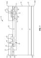
- FIG. 4is a cross-sectional view of a portion of the transistor semiconductor die 10 according to one embodiment of the present disclosure.
- the transistor semiconductor die 10includes a substrate 20, a drift layer 22 on the substrate 20, a number of implants 24 in the drift layer 22, a top metallization layer 26, and a bottom metallization layer 28.
- the transistor device Q igis provided as a vertical MOSFET including a pair of junction implants 30 in the drift layer 22 such that the junction implants 30 are separated by a JFET gap 32.
- a gate contact 34 on top of a gate oxide layer 36runs between the junction implants 30 on a surface of the drift layer 22 opposite the substrate 20.
- a source contact 38(which may also be the second current terminal 14) also contacts each one of the junction implants 30 on the surface of the drift layer 22 opposite the substrate.
- a drain contact 40(which may also be the first current terminal 12) is on the substrate 20 opposite the drift layer 22.
- the source contact 38is provided by a portion of the top metallization layer 26.
- the drain contact 40is provided by the bottom metallization layer 28.
- the control terminal 16is provided by a portion of the top metallization layer 26. While not shown, the control terminal 16 is coupled to the gate contact 34 of the transistor device Q ig on a plane not shown in the cross-section (e.g., via a gate runner 42 provided on a field oxide layer 44 below the top metallization layer 26). The control terminal 16 is also coupled to the source contact 38 of the transistor device Q ig through a number of P-N junctions 46 formed in the drift layer 22. Each one of these P-N junctions 46 forms one of the short circuit protection diodes D sc discussed above with respect to Figure 2 .
- the top metallization layer 26is appropriately patterned to form connections between the control terminal 16 and the source contact 38 through the P-N junctions 46 as shown.
- An intermetal dielectric layer 48may insulate different portions of the top metallization layer 26 to form the desired connection pattern.
- the transistor device Q igmay comprise any number of cells coupled together to provide a desired forward current rating of the transistor semiconductor die 10.
- the short circuit protection diodes D scare shown one next to another in the drift layer 22 in Figure 4
- the short circuit protection diodes D scmay be distributed in any suitable manner in the transistor semiconductor die 10.
- the short circuit protection diodes D scmay be distributed between different cells of the transistor device Q ig in a pattern in order to reduce the total active area devoted to the short circuit protection diodes D sc .
- the short circuit protection diodes D scwill consume very little area when compared to the transistor device Q ig and thus will have a minimal impact on the total active area of the transistor semiconductor die 10.
- Figure 5shows the transistor semiconductor die 10 according to an additional embodiment of the present disclosure.
- the transistor semiconductor die 10 shown in Figure 5is substantially similar to that shown in Figure 4 , except that the short circuit protection diodes D sc are provided as a number of P-N junctions 50 formed in an additional semiconductor layer 52 (e.g., a polysilicon layer) that is provided on the drift layer 22 (with the field oxide layer 44 between the additional semiconductor layer 52 and the drift layer 22 to avoid interaction between the layers).
- a number of metal jumpers 53may be provided between each adjacent P-N junction 50.
- the short circuit protection diodes D scmay be Zener diodes.
- the short circuit protection diodes D scare coupled in series cathode-to-anode between the insulted gate terminal 16 and the second current terminal 14 such that a cathode of a first one of the short circuit protection diodes D sc is coupled to the control terminal 16 and an anode of a last one of the short circuit protection diodes D sc is coupled to the second current terminal 14.
- the P-N junctions 50 in Figure 5may be reversed such that they are coupled anode-to-cathode between the insulated gate terminal 16 and the second current terminal 14 as shown.
- Providing the short circuit protection diodes D sc in the additional semiconductor layer 52 that is provided on the drift layer 22may allow a reduction or elimination of the active area devoted to the short circuit protection circuitry 18, since the short circuit protection diodes D sc can be moved over the transistor device Q ig in some embodiments.
- FIG 6is a schematic representation of the transistor semiconductor die 10 according to an additional embodiment of the present disclosure.
- the transistor semiconductor die 10 shown in Figure 6is substantially similar to that shown in Figure 2 , except that the short circuit protection circuitry 18 further includes a short circuit protection resistive element R sc coupled in series with the short circuit protection diodes D sc .
- the short circuit protection resistive element R scmay be used to achieve a precise voltage drop across the short circuit protection circuitry 18 that may be difficult to achieve using diodes alone.
- the short circuit protection circuitry 18may be provided with a negative temperature coefficient with respect to the resistance thereof, such that as the temperature of the transistor semiconductor die 10 increases, the resistance of the short circuit protection resistive element R sc decreases.
- Figure 7is a cross-sectional view of a portion of the transistor semiconductor die 10 according to an additional embodiment of the present disclosure.
- the transistor semiconductor die 10 shown in Figure 7is substantially similar to that shown in Figure 4 , except that the transistor semiconductor die 10 further includes the short circuit protection resistive element R sc coupled between the control terminal 16 and the second current terminal 14.
- the short circuit protection resistive element R scmay be implemented using a deep N-doped well 54. Providing the short circuit protection resistive element R sc in this manner may ensure a negative temperature coefficient with respect to resistance.
- the short circuit protection resistive element R scmay be implemented using a highly doped polysilicon resistor, a metal resistor with sufficiently high positive temperature coefficient with respect to resistance, or any other suitable type of resistive element.
- FIG 8is a schematic representation of the transistor semiconductor die 10 according to an additional embodiment of the present disclosure.
- the transistor semiconductor die 10 shown in Figure 8is substantially similar to that shown in Figure 1 , except that the transistor semiconductor die 10 further includes a gate resistive element R g coupled between the control terminal 16 and a gate of the transistor device Q ig .
- the gate resistive element R gis provided with a positive temperature coefficient with respect to a resistance thereof. In other words, a resistance of the gate resistive element R g increases as a temperature of the transistor semiconductor die 10 increases. Note that this functionality requires adequate thermal coupling between the short circuit protection circuitry 18 and the current carrying portion of the transistor semiconductor die 10. This may reduce a gate drive current in the event of a short circuit event, thereby enhancing the action of the short circuit protection circuitry 18.
- FIG. 9shows a schematic view of the transistor semiconductor die 10 wherein the transistor device Q ig is an IGBT instead of a MOSFET.
- the first current terminal 12is a collector terminal and the second current terminal 14 is an emitter terminal.
- FIG. 10shows a schematic view of the transistor semiconductor die 10 wherein the transistor device Q ig is a BJT instead of a MOSFET.
- the first current terminal 12is a collector terminal
- the second current terminal 14is an emitter terminal
- the control terminal 14is a base terminal.
- the MOSFET depicted in the cross-sectional views of the transistor semiconductor die 10 shown abovecan be readily replaced with a BJT.
- Figure 11shows a schematic view the transistor semiconductor die 10 wherein the transistor device Q ig is a JFET instead of a MOSFET.
- the first current terminal 12is a drain terminal
- the second current terminal 14is a source terminal
- the control terminal 16is a gate terminal.
Landscapes
- Engineering & Computer Science (AREA)
- Physics & Mathematics (AREA)
- General Physics & Mathematics (AREA)
- Electromagnetism (AREA)
- Radar, Positioning & Navigation (AREA)
- Automation & Control Theory (AREA)
- Microelectronics & Electronic Packaging (AREA)
- Nonlinear Science (AREA)
- Semiconductor Integrated Circuits (AREA)
- Metal-Oxide And Bipolar Metal-Oxide Semiconductor Integrated Circuits (AREA)
- Protection Of Static Devices (AREA)
Description
- The present disclosure is related to transistor semiconductor die, and in particular to transistor semiconductor die with improved protection against short circuit events.
- Transistor devices such as metal-oxide semiconductor field-effect transistors (MOSFETs), insulated gate bipolar transistors (IGBTs), junction field-effect transistors (JFETs), and bipolar junction transistors (BJTs) are often used in power electronics, in which they may be used to selectively deliver current to and from a load. In certain situations, a load may provide a short circuit across a transistor device. Such a short circuit event may cause the transistor device to fail.
- In recent years, there has been a push towards using wide bandgap semiconductor material systems for devices used in power electronics. For example, silicon carbide transistors are now in widespread use in power electronics. Compared to their silicon counterparts, silicon carbide transistors provide better performance, for example, by providing higher blocking voltage, lower on-state resistance, and lower switching loss. Silicon carbide transistors are also much smaller in size, and thus have higher current density. Accordingly, the short circuit withstand time, or the amount of time that a device can survive without failure during a short circuit event, of a silicon carbide transistor is much lower than that of a similar silicon device.
US2005/122748 discloses a gate of an IGBT connected to a gate terminal and one end of a clamping element connected to an anode terminal. A voltage higher than a clamping voltage is applied between the gate and the emitter, to thereby test the dielectric breakdown voltage of a gate insulating film of the IGBT. The IGBT is eliminated which has a gate insulating film at a dielectric breakdown voltage failing to fall within its proper distribution range. Thereafter, a gate terminal and an anode terminal are wire bonded in the normal IGBT.EP0224274 discloses a semiconductor substrate with a power region and a control region. The control region is located in the center portion of the substrate, and the power region surrounds the control region and is separated therefrom. A vertical type, MOS transistor is formed on the power region. An insulation film is formed on part of the control region. A polycrystalline silicon diode is formed on the insulation film. A control section comprising a lateral type, MOS transistor is formed on the control region. The lateral type, MOS transistor is connected to receive a signal from the polycrystalline silicon diode. Further, a polycrystalline silicon resistor, which determines a circuit constant, is formed on the insulation film. The MOS transistor protects the active semiconductor element in response to a signal suppled from said heat-sensitive element and showing that the temperature of said semi-conductor substrate has risen above a predetermined value.EP3419170 discloses a protection circuit including: a high-side switch connected to a power terminal to which a predetermined power supply voltage VBB is supplied from an onboard battery; and an NMOS transistor connected to the high-side switch and configured to prevent an electrical conduction to the high-side switch when the onboard battery is reverse-connected to the power terminal. A semiconductor integrated circuit is protected from a breakdown due to the reverse connection of the external power supply.EP1063757 discloses a MOSFET containing a voltage clamp including one or more diodes which connects its gate and source. The voltage clamp is designed to break down at a predetermined voltage and thereby protect the gate oxide layer from damage as a result of an excessive source-to-gate voltage. The voltage clamp generally contains one or more parallel branches connected between the source and gate terminals of the MOSFET. Each branch contains at least one diode and in many cases a series of diodes that, depending on the clamping voltage desired, are connected so that they either break down or conduct in a forward direction when the gate-to-source voltage reaches a selected level. To achieve a lower clamping voltage the diode or diodes are typically connected so that they conduct in a forward direction, and to achieve a higher clamping voltage the diode or diodes are connected so that they undergo avalanche breakdown. A given branch can contain diodes that are connected in different directions (e.g., a diode pair connected anode-to-anode) in order to obtain a desired clamping voltage. If more than one branch is used, the diodes in one branch provide a clamping voltage that is less than the diodes in the other branch. A resistance can be connected in series with the diodes which provide the lower clamping voltage to limit the amount of current through those diodes and thereby prevent them from burning in the event that a current is forced through them. Diodes in certain branches may protect the gate oxide layer from gate voltage swings in one direction while diodes in other branches may protect the gate oxide layer from voltage swings in the other direction. A parallel combination of a resistor and a diode is connected in the path between the gate terminal and the gate of the MOSFET. The diode is reverse-biased, forcing the current through the resistor, when the gate is driven to turn the MOSFET on and conducts in a forward direction, shunting the current around the resistor, when the gate is driven to turn the MOSFET off. This arrangement provides a differential turn-on, turn-off characteristic. The relatively slow turn-on time prevents voltage overshoot and ringing that can occur in inductive circuits when the MOSFET is turned on.- In light of the above, there is a present need for silicon carbide transistor devices with improved short circuit protection.
- According to a first aspect, there is provided a transistor semiconductor die according to claim 1.
- The accompanying drawing figures incorporated in and forming a part of this specification illustrate several aspects of the disclosure, and together with the description serve to explain the principles of the disclosure.
Figure 1 is a schematic representation of a transistor semiconductor die according to one embodiment of the present disclosure.Figure 2 is a schematic representation of a transistor semiconductor die according to one embodiment of the present disclosure.Figure 3 is a graph illustrating a relationship between drain-source voltage, drain-source current, and gate-source voltage for a metal-oxide semiconductor field-effect transistor (MOSFET) according to one embodiment of the present disclosure.Figure 4 is a cross-sectional view of a portion of a transistor semiconductor die according to one embodiment of the present disclosure.Figure 5 is a cross-sectional view of a portion of a transistor semiconductor die according to one embodiment of the present disclosure.Figure 6 is a schematic representation of a transistor semiconductor die according to one embodiment of the present disclosure.Figure 7 is a cross-sectional view of a transistor semiconductor die according to one embodiment of the present disclosure.Figure 8 is a schematic representation of a transistor semiconductor die according to one embodiment of the present disclosure.Figure 9 is a schematic representation of a transistor semiconductor die according to one embodiment of the present disclosure.Figure 10 is a schematic representation of a transistor semiconductor die according to one embodiment of the present disclosure.Figure 11 is a schematic representation of a transistor semiconductor die according to one embodiment of the present disclosure.- It will be understood that, although the terms first, second, etc. may be used herein to describe various elements, these elements should not be limited by these terms. These terms are only used to distinguish one element from another. For example, a first element could be termed a second element, and, similarly, a second element could be termed a first element, without departing from the scope of the present disclosure. As used herein, the term "and/or" includes any and all combinations of one or more of the associated listed items.
- It will be understood that when an element such as a layer, region, or substrate is referred to as being "on" or extending "onto" another element, it can be directly on or extend directly onto the other element or intervening elements may also be present. In contrast, when an element is referred to as being "directly on" or extending "directly onto" another element, there are no intervening elements present. Likewise, it will be understood that when an element such as a layer, region, or substrate is referred to as being "over" or extending "over" another element, it can be directly over or extend directly over the other element or intervening elements may also be present. In contrast, when an element is referred to as being "directly over" or extending "directly over" another element, there are no intervening elements present. It will also be understood that when an element is referred to as being "connected" or "coupled" to another element, it can be directly connected or coupled to the other element or intervening elements may be present. In contrast, when an element is referred to as being "directly connected" or "directly coupled" to another element, there are no intervening elements present.
- Relative terms such as "below" or "above" or "upper" or "lower" or "horizontal" or "vertical" may be used herein to describe a relationship of one element, layer, or region to another element, layer, or region as illustrated in the Figures. It will be understood that these terms and those discussed above are intended to encompass different orientations of the device in addition to the orientation depicted in the Figures.
- The terminology used herein is for the purpose of describing particular embodiments only and is not intended to be limiting of the disclosure. As used herein, the singular forms "a," "an," and "the" are intended to include the plural forms as well, unless the context clearly indicates otherwise. It will be further understood that the terms "comprises," "comprising," "includes," and/or "including" when used herein specify the presence of stated features, integers, steps, operations, elements, and/or components, but do not preclude the presence or addition of one or more other features, integers, steps, operations, elements, components, and/or groups thereof.
- Unless otherwise defined, all terms (including technical and scientific terms) used herein have the same meaning as commonly understood by one of ordinary skill in the art to which this disclosure belongs. It will be further understood that terms used herein should be interpreted as having a meaning that is consistent with their meaning in the context of this specification and the relevant art and will not be interpreted in an idealized or overly formal sense unless expressly so defined herein.
Figure 1 shows a schematic representation of a transistor semiconductor die 10 according to one embodiment of the present disclosure. The transistor semiconductor die 10 includes a firstcurrent terminal 12, a secondcurrent terminal 14, and acontrol terminal 16. A semiconductor structure between the firstcurrent terminal 12, the secondcurrent terminal 14, and thecontrol terminal 16 forms a transistor device Qig such that a resistance between the firstcurrent terminal 12 and the secondcurrent terminal 14 is based on a control signal CNT provided at thecontrol terminal 16. As shown inFigure 1 , the transistor device Qig is a metal-oxide semiconductor field-effect transistor (MOSFET). Accordingly, the firstcurrent terminal 12 is a drain terminal, the secondcurrent terminal 14 is a source terminal, and thecontrol terminal 16 is a gate terminal. However, the principles of the present disclosure apply equally to any transistor device such as an insulated gate bipolar transistor (IGBT). In the case of an IGBT, the firstcurrent terminal 12 is a collector terminal, the secondcurrent terminal 14 is an emitter terminal, and thecontrol terminal 16 is a gate terminal. Since the transistor device Qig may be used for power electronics, a freewheeling anti-parallel diode Dfw may be coupled in anti-parallel with the transistor device Qig so that current can be conducted bidirectionally between the firstcurrent terminal 12 and the secondcurrent terminal 14. In various embodiments, the freewheeling diode Dfw may be external from the transistor device Qig, or may be internal to the transistor device Qig, e.g., a body diode.- While the transistor device Qig is shown herein as an insulated gate device, the principles of the present disclosure apply equally to any transistor device such as bipolar junction transistors (BJTs), and junction field-effect transistors (JFETs). In the case of a BJT, the first
current terminal 12 is a collector terminal, the secondcurrent terminal 14 is an emitter terminal, and thecontrol terminal 16 is a base terminal. In the case of a JFET, the firstcurrent terminal 12 is a drain terminal, the secondcurrent terminal 14 is a source terminal, and thecontrol terminal 16 is a gate terminal. Further, the transistor device Qig may be a thyristor. In the case of a thyristor, the firstcurrent terminal 12 is an anode, the secondcurrent terminal 14 is a cathode, and thecontrol terminal 16 is a gate terminal. - The transistor semiconductor die 10 may utilize a wide bandgap material system such as silicon carbide. As discussed above, the silicon carbide transistor semiconductor die 10 may be more sensitive to short circuit events than their silicon counterparts due to the smaller size and higher current density thereof. Accordingly, short
circuit protection circuitry 18 is coupled between thecontrol terminal 16 and the secondcurrent terminal 14. The shortcircuit protection circuitry 18 is configured to operate in a normal mode of operation and a short circuit protection mode of operation. In the normal mode of operation, the shortcircuit protection circuitry 18 is configured to provide a voltage drop between thecontrol terminal 16 and the secondcurrent terminal 14 that is greater than a voltage of the control signal CNT. In the short circuit protection mode of operation, the shortcircuit protection circuitry 18 is configured to provide a voltage drop between thecontrol terminal 16 and the secondcurrent terminal 14 that is less than a voltage of the control signal CNT. In the normal mode of operation when a voltage drop across the shortcircuit protection circuitry 18 is greater than a voltage of the control signal CNT, the operation of the transistor device Qig is relatively unaffected. In the short circuit protection mode of operation when a voltage drop across the shortcircuit protection circuitry 18 is less than a voltage of the control signal CNT, a voltage at thecontrol terminal 16 is lowered such that voltage between thecontrol terminal 16 and the second current terminal 14 (i.e., the gate-to-source voltage of the transistor device Qig) is reduced, which in turn partially or completely shuts off the device. Shutting off the transistor device Qig protects the device during a short circuit event in order to prevent a failure. - One way in which the above-mentioned functionality may be accomplished is by providing the short
circuit protection circuitry 18 such that it has a negative temperature coefficient with respect to a voltage drop across the shortcircuit protection circuitry 18. In other words, the shortcircuit protection circuitry 18 may be provided such that a voltage drop across the shortcircuit protection circuitry 18 decreases as temperature increases. Since during a short circuit event a temperature of the transistor semiconductor die 10 will rapidly increase far above normal operating temperatures thereof, the shortcircuit protection circuitry 18 may significantly reduce a voltage drop between thecontrol terminal 16 and the secondcurrent terminal 14 only when a short circuit event occurs. Note that this functionality requires adequate thermal coupling between the shortcircuit protection circuitry 18 and the current carrying portion of the transistor semiconductor die 10. - Notably, the short
circuit protection circuitry 18 is located on the transistor semiconductor die 10. As discussed in detail below, the shortcircuit protection circuitry 18 takes up minimal area on the transistor semiconductor die 10 and may be capable of extending a short circuit withstand time of the transistor semiconductor die 10 significantly, and in some cases indefinitely. Figure 2 is a schematic representation of the transistor semiconductor die 10 showing details of the shortcircuit protection circuitry 18 according to one embodiment of the present disclosure. As shown inFigure 2 , the shortcircuit protection circuitry 18 may include a number of short circuit protection diodes Dsc coupled in series between thecontrol terminal 16 and the secondcurrent terminal 14. In particular, the short circuit protection diodes Dsc are coupled anode-to-cathode between thecontrol terminal 16 and the secondcurrent terminal 14 such that an anode of a first one of the short circuit protection diodes Dsc is coupled to thecontrol terminal 16 and a cathode of a last one of the short circuit protection diodes Dsc is coupled to the secondcurrent terminal 14. As discussed above, the short circuit protection diodes Dsc may be provided with a negative temperature coefficient (e.g., an exponential negative temperature coefficient) with respect to a forward voltage drop thereof. In other words, the short circuit protection diodes Dsc may be provided such that a forward voltage drop across the diodes decreases as temperature increases. Such a negative temperature coefficient is naturally present in silicon carbide diodes. The negative temperature coefficient enables a voltage drop across the short circuit protection diodes Dsc to be greater than a voltage of the control signal CNT in the normal mode of operation (and thus not interfere with the operation of the transistor device Qig) and be less than a voltage of the control signal CNT in the short circuit protection mode of operation (thus partially or completely turning off the transistor device Qig). Note that this functionality requires adequate thermal coupling between the shortcircuit protection circuitry 18 and the current carrying portion of the transistor semiconductor die 10. The number of short circuit protection diodes Dsc may be chosen such that when a temperature of the transistor semiconductor die 10 is below a short circuit threshold temperature a voltage drop across the short circuit protection diodes Dsc is greater than or equal to a voltage of the control signal CNT and when a temperature of the transistor semiconductor die 10 is above the short circuit threshold temperature a voltage drop across the short circuit protection diodes Dsc is significantly less than the voltage of the control signal CNT such that a voltage at thecontrol terminal 16 is lowered enough to partially or completely turn off the transistor device Qig.- In addition to protecting the transistor device Qig against short circuit events, the short
circuit protection circuitry 18 also clamps the maximum voltage of the gate to the combined forward voltage drop of the short circuit protection diodes Dsc. This has the additional benefits of protecting the transistor device Qig against electrostatic discharge (ESD) and provides voltage overshoot protection for the gate of the transistor device Qig. - The short
circuit protection circuitry 18 may enable significant improvements in the short circuit withstand time of the transistor semiconductor die 10. As discussed herein, the shortcircuit protection circuitry 18 may require minimal active area on the transistor semiconductor die 10. In various embodiments, an on-state resistance of the transistor semiconductor die 10 may be between 0.1 mΩ/cm2 and 3.0mΩ/cm2, a blocking voltage of the transistor semiconductor die 10 may be between 600V and 10kV, and a short circuit withstand time of the transistor semiconductor die 10 may be greater than 3µs. Notably, the on-state resistance of the transistor semiconductor die 10 may fall anywhere in the above range, such as between 0.5mΩ/cm2 and 3.0mΩ/cm2, between 1.0mΩ/cm2 and 3.0mΩ/cm2, between 1.5mΩ/cm2 and 3.0mΩ/cm2, between 2.0mΩ/cm2 and 3.0mΩ/cm2, between 2.5mΩ/cm2 and 3.0mΩ/cm2, and the like. The blocking voltage of the transistor semiconductor die 10 may similarly fall anywhere inside the above range, such as between 600V and 1kV, between 600V and 2kV, between 600V and 5kV, between 1kV and 5kV, between 5kV and 10kV, and the like. A relationship between the on-state resistance and the blocking voltage of the transistor semiconductor die 10 may be expressed according to Equation (1):
- The short circuit withstand time of the transistor semiconductor die 10 may be less than 10s in some embodiments, but the principles of the present disclosure may also enable the transistor semiconductor die 10 to indefinitely withstand a short circuit event in some circumstances. The short circuit withstand time of the transistor semiconductor die 10 may fall anywhere in the above ranges such that the short circuit withstand time is between 4µs and 10s, between 5µs and 10s, between 10µs and 10s, between 50µs and 10s, between 5ms and 10s, between 10ms and 10s, between 50ms and 10s, between 1s and 10s, and the like.
Figure 3 is a graph illustrating a relationship between drain-source voltage, drain-source current, and gate-source voltage in a MOSFET. As shown, a relationship between drain-source voltage and drain-source current is dependent on gate-source voltage such that as the gate-source voltage increases, a steepness of the curve between drain-source voltage and drain-source current increases. Accordingly, higher gate-source voltages will lead to higher drain-source currents during a short circuit event. When a drain-source current becomes high enough, the device will fail. By reducing the gate-source voltage during a short circuit event, the drain-source current is significantly reduced such that a failure of the device can be prevented.Figure 4 is a cross-sectional view of a portion of the transistor semiconductor die 10 according to one embodiment of the present disclosure. The transistor semiconductor die 10 includes asubstrate 20, adrift layer 22 on thesubstrate 20, a number ofimplants 24 in thedrift layer 22, atop metallization layer 26, and abottom metallization layer 28. In particular, on the right side of the transistor semiconductor die 10 the transistor device Qig is provided as a vertical MOSFET including a pair ofjunction implants 30 in thedrift layer 22 such that thejunction implants 30 are separated by aJFET gap 32. Agate contact 34 on top of agate oxide layer 36 runs between thejunction implants 30 on a surface of thedrift layer 22 opposite thesubstrate 20. A source contact 38 (which may also be the second current terminal 14) also contacts each one of thejunction implants 30 on the surface of thedrift layer 22 opposite the substrate. A drain contact 40 (which may also be the first current terminal 12) is on thesubstrate 20 opposite thedrift layer 22. The source contact 38 is provided by a portion of thetop metallization layer 26. Thedrain contact 40 is provided by thebottom metallization layer 28.- On the left side of the transistor semiconductor die 10, the
control terminal 16 is provided by a portion of thetop metallization layer 26. While not shown, thecontrol terminal 16 is coupled to thegate contact 34 of the transistor device Qig on a plane not shown in the cross-section (e.g., via agate runner 42 provided on afield oxide layer 44 below the top metallization layer 26). Thecontrol terminal 16 is also coupled to the source contact 38 of the transistor device Qig through a number ofP-N junctions 46 formed in thedrift layer 22. Each one of theseP-N junctions 46 forms one of the short circuit protection diodes Dsc discussed above with respect toFigure 2 . Thetop metallization layer 26 is appropriately patterned to form connections between thecontrol terminal 16 and the source contact 38 through theP-N junctions 46 as shown. Anintermetal dielectric layer 48 may insulate different portions of thetop metallization layer 26 to form the desired connection pattern. - While only one unit cell of the transistor device Qig is shown in
Figure 4 , the transistor device Qig may comprise any number of cells coupled together to provide a desired forward current rating of the transistor semiconductor die 10. Further, while the short circuit protection diodes Dsc are shown one next to another in thedrift layer 22 inFigure 4 , the short circuit protection diodes Dsc may be distributed in any suitable manner in the transistor semiconductor die 10. For example, the short circuit protection diodes Dsc may be distributed between different cells of the transistor device Qig in a pattern in order to reduce the total active area devoted to the short circuit protection diodes Dsc. In general, the short circuit protection diodes Dsc will consume very little area when compared to the transistor device Qig and thus will have a minimal impact on the total active area of the transistor semiconductor die 10. Figure 5 shows the transistor semiconductor die 10 according to an additional embodiment of the present disclosure. The transistor semiconductor die 10 shown inFigure 5 is substantially similar to that shown inFigure 4 , except that the short circuit protection diodes Dsc are provided as a number ofP-N junctions 50 formed in an additional semiconductor layer 52 (e.g., a polysilicon layer) that is provided on the drift layer 22 (with thefield oxide layer 44 between theadditional semiconductor layer 52 and thedrift layer 22 to avoid interaction between the layers). A number ofmetal jumpers 53 may be provided between eachadjacent P-N junction 50. In the embodiment shown inFigure 5 the short circuit protection diodes Dsc may be Zener diodes. In such an embodiment, the short circuit protection diodes Dsc are coupled in series cathode-to-anode between the insultedgate terminal 16 and the secondcurrent terminal 14 such that a cathode of a first one of the short circuit protection diodes Dsc is coupled to thecontrol terminal 16 and an anode of a last one of the short circuit protection diodes Dsc is coupled to the secondcurrent terminal 14. However, theP-N junctions 50 inFigure 5 may be reversed such that they are coupled anode-to-cathode between theinsulated gate terminal 16 and the secondcurrent terminal 14 as shown. Providing the short circuit protection diodes Dsc in theadditional semiconductor layer 52 that is provided on thedrift layer 22 may allow a reduction or elimination of the active area devoted to the shortcircuit protection circuitry 18, since the short circuit protection diodes Dsc can be moved over the transistor device Qig in some embodiments.Figure 6 is a schematic representation of the transistor semiconductor die 10 according to an additional embodiment of the present disclosure. The transistor semiconductor die 10 shown inFigure 6 is substantially similar to that shown inFigure 2 , except that the shortcircuit protection circuitry 18 further includes a short circuit protection resistive element Rsc coupled in series with the short circuit protection diodes Dsc. The short circuit protection resistive element Rsc may be used to achieve a precise voltage drop across the shortcircuit protection circuitry 18 that may be difficult to achieve using diodes alone. Since using only diodes in the shortcircuit protection circuitry 18 effectively limits the total voltage drop across the shortcircuit protection circuitry 18 to integer multiples of the forward voltage drop of the diodes, providing the short circuit protection resistive element Rsc allows for more precise tuning of the voltage drop across the shortcircuit protection circuitry 18. The shortcircuit protection circuitry 18 may be provided with a negative temperature coefficient with respect to the resistance thereof, such that as the temperature of the transistor semiconductor die 10 increases, the resistance of the short circuit protection resistive element Rsc decreases.Figure 7 is a cross-sectional view of a portion of the transistor semiconductor die 10 according to an additional embodiment of the present disclosure. The transistor semiconductor die 10 shown inFigure 7 is substantially similar to that shown inFigure 4 , except that the transistor semiconductor die 10 further includes the short circuit protection resistive element Rsc coupled between thecontrol terminal 16 and the secondcurrent terminal 14. The short circuit protection resistive element Rsc may be implemented using a deep N-dopedwell 54. Providing the short circuit protection resistive element Rsc in this manner may ensure a negative temperature coefficient with respect to resistance. While not shown, in other embodiments, the short circuit protection resistive element Rsc may be implemented using a highly doped polysilicon resistor, a metal resistor with sufficiently high positive temperature coefficient with respect to resistance, or any other suitable type of resistive element.Figure 8 is a schematic representation of the transistor semiconductor die 10 according to an additional embodiment of the present disclosure. The transistor semiconductor die 10 shown inFigure 8 is substantially similar to that shown inFigure 1 , except that the transistor semiconductor die 10 further includes a gate resistive element Rg coupled between thecontrol terminal 16 and a gate of the transistor device Qig. The gate resistive element Rg is provided with a positive temperature coefficient with respect to a resistance thereof. In other words, a resistance of the gate resistive element Rg increases as a temperature of the transistor semiconductor die 10 increases. Note that this functionality requires adequate thermal coupling between the shortcircuit protection circuitry 18 and the current carrying portion of the transistor semiconductor die 10. This may reduce a gate drive current in the event of a short circuit event, thereby enhancing the action of the shortcircuit protection circuitry 18.- As discussed above, while the foregoing examples of transistor semiconductor die 10 are primarily shown depicting the transistor device Qig as a MOSFET, the principles of the present disclosure apply equally to any type of transistor devices including IGBTs, BJTs, JFETs, and the like. Accordingly, for the sake of completeness
Figure 9 shows a schematic view of the transistor semiconductor die 10 wherein the transistor device Qig is an IGBT instead of a MOSFET. In this case, the firstcurrent terminal 12 is a collector terminal and the secondcurrent terminal 14 is an emitter terminal. Those skilled in the art will readily appreciate that the MOSFET depicted in the cross-sectional views of the transistor semiconductor die 10 shown above can be readily replaced with an IGBT, for example, by adding an injector layer between thesubstrate 20 and thedrift layer 22.Figure 10 shows a schematic view of the transistor semiconductor die 10 wherein the transistor device Qig is a BJT instead of a MOSFET. In this case, the firstcurrent terminal 12 is a collector terminal, the secondcurrent terminal 14 is an emitter terminal, and thecontrol terminal 14 is a base terminal. Those skilled in the art will readily appreciate that the MOSFET depicted in the cross-sectional views of the transistor semiconductor die 10 shown above can be readily replaced with a BJT.Figure 11 shows a schematic view the transistor semiconductor die 10 wherein the transistor device Qig is a JFET instead of a MOSFET. In this case, the firstcurrent terminal 12 is a drain terminal, the secondcurrent terminal 14 is a source terminal, and thecontrol terminal 16 is a gate terminal. Those skilled in the art will readily appreciate that the MOSFET depicted in the cross-sectional views of the transistor semiconductor die 10 shown above can be readily replaced with a JFET.

Claims (15)
- A transistor semiconductor die comprising:a first current terminal (12, 40) and a second current terminal (14, 38);a control terminal (16);a semiconductor structure comprising a drift layer (22), wherein the semiconductor structure is between the first current terminal, the second current terminal, and the control terminal, the semiconductor structure configured such that a resistance between the first current terminal and the second current terminal is based on a control signal provided at the control terminal; andshort circuit protection circuitry (Dsc, 46) that resides within the drift layer, wherein the short circuit protection circuitry comprises a plurality of diodes coupled between the control terminal and the second current terminal and configured such that:in a normal mode of operation, a voltage drop between the control terminal and the second current terminal is greater than a voltage of the control signal; andin a short circuit protection mode of operation, a voltage drop between the control terminal and the second current terminal is less than a voltage of the control signal.
- The transistor semiconductor die of claim 1 wherein the plurality of diodes are provided by a plurality of implanted regions in the semiconductor structure.
- The transistor semiconductor die of claim 1 further comprising a resistive element (Rsc, 54) coupled between the short circuit protection circuitry and the control terminal.
- The transistor semiconductor die of claim 3 wherein:the plurality of diodes have a negative temperature coefficient with respect to a voltage drop across the plurality of diodes; andthe resistive element has a positive temperature coefficient with respect to a resistance thereof.
- The transistor semiconductor die of claim 1 wherein the plurality of diodes have a negative temperature coefficient with respect to a voltage drop across the plurality of diodes.
- The transistor semiconductor die of claim 1 wherein the plurality of diodes are coupled in series such that an anode of a first one of the plurality of diodes is coupled to the control terminal and a cathode of a last one of the plurality of diodes is coupled to the second current terminal.
- The transistor semiconductor die of claim 6 wherein the plurality of diodes are PN diodes or Schottky diodes.
- The transistor semiconductor die of claim 1 wherein the plurality of diodes are Zener diodes coupled in series such that a cathode of a first one of the plurality of diodes is coupled to the control terminal and an anode of a last one of the plurality of diodes is coupled to the second current terminal.
- The transistor semiconductor die of claim 1 wherein the semiconductor structure comprises silicon carbide.
- The transistor semiconductor die of claim 9 wherein the semiconductor structure provides a metal-oxide semiconductor field-effect transistor, MOSFET, such that the first current terminal is a drain terminal and the second current terminal is a source terminal.
- The transistor semiconductor die of claim 9 wherein the semiconductor structure provides an insulated gate bipolar transistor, IGBT, such that the first current terminal is a collector terminal and the second current terminal is an emitter terminal.
- The transistor semiconductor die of claim 1 wherein:the transistor semiconductor die is configured to operate in the normal mode of operation when a temperature of the semiconductor structure is below a short circuit threshold temperature; andthe transistor semiconductor die is configured to operate in the short circuit protection mode of operation when a temperature of the semiconductor structure is above the short circuit threshold temperature.
- The transistor semiconductor die of claim 1 wherein the voltage drop between the control terminal and the second current terminal provided by the short circuit protection circuitry has a negative temperature coefficient.
- The transistor semiconductor die of claim 1 wherein an on-state resistance of the transistor semiconductor die is less than 3.0mΩ/cm2, a blocking voltage of the transistor semiconductor die is greater than 600V, and a short circuit withstand time of the transistor semiconductor die is greater than 3µs.
- The transistor semiconductor die of claim 14 wherein the on-state resistance of the transistor semiconductor die is greater than 0.1mΩ/cm2, the blocking voltage of the transistor semiconductor die is less than 10kV, and a short circuit withstand time of the transistor semiconductor die is less than 10s.
Priority Applications (1)
| Application Number | Priority Date | Filing Date | Title |
|---|---|---|---|
| EP24170557.3AEP4380056A3 (en) | 2019-06-21 | 2020-06-05 | Device design for short circuit protection of transistors |
Applications Claiming Priority (2)
| Application Number | Priority Date | Filing Date | Title |
|---|---|---|---|
| US16/448,538US11579645B2 (en) | 2019-06-21 | 2019-06-21 | Device design for short-circuitry protection circuitry within transistors |
| PCT/US2020/036251WO2020256962A1 (en) | 2019-06-21 | 2020-06-05 | Device design for short-circuit protection of transistors |
Related Child Applications (2)
| Application Number | Title | Priority Date | Filing Date |
|---|---|---|---|
| EP24170557.3ADivisionEP4380056A3 (en) | 2019-06-21 | 2020-06-05 | Device design for short circuit protection of transistors |
| EP24170557.3ADivision-IntoEP4380056A3 (en) | 2019-06-21 | 2020-06-05 | Device design for short circuit protection of transistors |
Publications (2)
| Publication Number | Publication Date |
|---|---|
| EP3987661A1 EP3987661A1 (en) | 2022-04-27 |
| EP3987661B1true EP3987661B1 (en) | 2024-05-29 |
Family
ID=71846486
Family Applications (2)
| Application Number | Title | Priority Date | Filing Date |
|---|---|---|---|
| EP20747541.9AActiveEP3987661B1 (en) | 2019-06-21 | 2020-06-05 | Device design for short circuit protection of transistors |
| EP24170557.3APendingEP4380056A3 (en) | 2019-06-21 | 2020-06-05 | Device design for short circuit protection of transistors |
Family Applications After (1)
| Application Number | Title | Priority Date | Filing Date |
|---|---|---|---|
| EP24170557.3APendingEP4380056A3 (en) | 2019-06-21 | 2020-06-05 | Device design for short circuit protection of transistors |
Country Status (4)
| Country | Link |
|---|---|
| US (2) | US11579645B2 (en) |
| EP (2) | EP3987661B1 (en) |
| JP (2) | JP7362790B2 (en) |
| WO (1) | WO2020256962A1 (en) |
Families Citing this family (6)
| Publication number | Priority date | Publication date | Assignee | Title |
|---|---|---|---|---|
| DE102020114698A1 (en)* | 2020-06-03 | 2021-12-09 | HELLA GmbH & Co. KGaA | Control device for an electrical load, in particular for a motor vehicle |
| EP3975261A1 (en)* | 2020-09-29 | 2022-03-30 | Infineon Technologies Dresden GmbH & Co . KG | Voltage-controlled switching device with resistive path |
| JP7689428B2 (en)* | 2021-01-26 | 2025-06-06 | エイブリック株式会社 | Semiconductor Device |
| EP4105989A1 (en)* | 2021-06-16 | 2022-12-21 | Infineon Technologies AG | Semiconductor device with diode chain connected to gate metallization |
| CN114636910B (en)* | 2022-03-03 | 2025-09-02 | 杭州优迈科技有限公司 | Detection circuit of transistor |
| DE102024106190A1 (en) | 2024-03-04 | 2025-09-04 | Infineon Technologies Ag | Wide bandgap semiconductor device having a heat-sensitive element |
Family Cites Families (123)
| Publication number | Priority date | Publication date | Assignee | Title |
|---|---|---|---|---|
| JPS5272183A (en)* | 1975-12-12 | 1977-06-16 | Mitsubishi Electric Corp | Semiconductor device with protecting device |
| JPS6271275A (en)* | 1985-09-25 | 1987-04-01 | Toshiba Corp | semiconductor integrated circuit |
| JPH0693485B2 (en)* | 1985-11-29 | 1994-11-16 | 日本電装株式会社 | Semiconductor device |
| US5119162A (en)* | 1989-02-10 | 1992-06-02 | Texas Instruments Incorporated | Integrated power DMOS circuit with protection diode |
| US5311391A (en)* | 1993-05-04 | 1994-05-10 | Hewlett-Packard Company | Electrostatic discharge protection circuit with dynamic triggering |
| JP3243902B2 (en)* | 1993-09-17 | 2002-01-07 | 株式会社日立製作所 | Semiconductor device |
| JP2792417B2 (en)* | 1993-12-17 | 1998-09-03 | 日本電気株式会社 | Input protection circuit for semiconductor circuit |
| JP3265849B2 (en)* | 1994-09-16 | 2002-03-18 | 富士電機株式会社 | Self-extinguishing element with overheat protection device |
| GB9424666D0 (en)* | 1994-12-07 | 1995-02-01 | Philips Electronics Uk Ltd | A protected switch |
| GB9426007D0 (en)* | 1994-12-22 | 1995-02-22 | Philips Electronics Uk Ltd | A power semiconductor switch |
| US5825603A (en)* | 1995-12-21 | 1998-10-20 | Intel Corporaiton | Method and apparatus for providing electrostatic discharge protection for high voltage inputs |
| US5812006A (en)* | 1996-10-29 | 1998-09-22 | Texas Instruments Incorporated | Optimized power output clamping structure |
| US5894200A (en)* | 1997-03-26 | 1999-04-13 | Goodale, Jr.; Garold Joseph | Two terminal method of and apparatus for improving electrical and light producing efficiency in low voltage direct current incandescent lamp intensity control |
| US5978192A (en)* | 1997-11-05 | 1999-11-02 | Harris Corporation | Schmitt trigger-configured ESD protection circuit |
| US6172383B1 (en) | 1997-12-31 | 2001-01-09 | Siliconix Incorporated | Power MOSFET having voltage-clamped gate |
| JPH11251594A (en)* | 1997-12-31 | 1999-09-17 | Siliconix Inc | Power MOSFET with voltage clamped gate |
| FR2809545B1 (en)* | 2000-05-23 | 2002-10-11 | St Microelectronics Sa | SERIAL PROTECTION DEVICE FOR A DATA OR ENERGY TRANSMISSION LINE |
| JP3502371B2 (en)* | 2000-10-23 | 2004-03-02 | 松下電器産業株式会社 | Semiconductor element |
| US7345342B2 (en)* | 2001-01-30 | 2008-03-18 | Fairchild Semiconductor Corporation | Power semiconductor devices and methods of manufacture |
| JP4846106B2 (en)* | 2001-02-16 | 2011-12-28 | 三菱電機株式会社 | Field effect semiconductor device and method for manufacturing the same |
| JP3708489B2 (en)* | 2002-01-30 | 2005-10-19 | 株式会社シマノ | Bicycle dynamo voltage clamp circuit |
| US6906399B2 (en)* | 2002-11-04 | 2005-06-14 | Delphi Technologies, Inc. | Integrated circuit including semiconductor power device and electrically isolated thermal sensor |
| JP4250412B2 (en)* | 2002-12-13 | 2009-04-08 | 三菱電機株式会社 | Semiconductor device |
| US6906386B2 (en)* | 2002-12-20 | 2005-06-14 | Advanced Analogic Technologies, Inc. | Testable electrostatic discharge protection circuits |
| JP2005175054A (en) | 2003-12-09 | 2005-06-30 | Mitsubishi Electric Corp | Semiconductor device and manufacturing method thereof |
| US7202528B2 (en)* | 2004-12-01 | 2007-04-10 | Semisouth Laboratories, Inc. | Normally-off integrated JFET power switches in wide bandgap semiconductors and methods of making |
| JP4252511B2 (en) | 2004-07-30 | 2009-04-08 | 新日本無線株式会社 | Semiconductor device |
| US7342440B2 (en)* | 2005-03-04 | 2008-03-11 | Infineon Technologies Austria Ag | Current regulator having a transistor and a measuring resistor |
| US7629631B2 (en)* | 2005-06-21 | 2009-12-08 | Hamza Yilmaz | High voltage semiconductor devices with JFET regions containing dielectrically isolated junctions |
| US7484074B2 (en)* | 2006-01-18 | 2009-01-27 | International Business Machines Corporation | Method and system for automatically distributing real memory between virtual memory page sizes |
| EP1997142A1 (en)* | 2006-03-13 | 2008-12-03 | Freescale Semiconductor, Inc. | Semiconductor device structure and integrated circuit therefor |
| US7564666B2 (en)* | 2006-05-02 | 2009-07-21 | Semiconductor Components Industries, L.L.C. | Shunt protection circuit and method therefor |
| US7982528B2 (en)* | 2006-05-18 | 2011-07-19 | Stmicroelectronics, S.R.L. | Three-terminal power device with high switching speed and manufacturing process |
| DE102007002377B4 (en)* | 2006-05-22 | 2011-12-01 | Texas Instruments Deutschland Gmbh | Integrated circuit device |
| JP2008172411A (en) | 2007-01-10 | 2008-07-24 | Sharp Corp | Semiconductor integrated circuit |
| US7511357B2 (en)* | 2007-04-20 | 2009-03-31 | Force-Mos Technology Corporation | Trenched MOSFETs with improved gate-drain (GD) clamp diodes |
| US20080272828A1 (en)* | 2007-05-03 | 2008-11-06 | Dsm Solutions, Inc. | Method and system for adaptive power management |
| JP5272183B2 (en) | 2007-09-27 | 2013-08-28 | Jx日鉱日石エネルギー株式会社 | Fuel cell reformer |
| JP5532538B2 (en)* | 2008-02-04 | 2014-06-25 | 三菱電機株式会社 | Protection circuit |
| US9620584B2 (en)* | 2009-08-31 | 2017-04-11 | Alpha And Omega Semiconductor Incorporated | Integrated Schottky diode in high voltage semiconductor device |
| US8829614B2 (en)* | 2009-08-31 | 2014-09-09 | Alpha And Omega Semiconductor Incorporated | Integrated Schottky diode in high voltage semiconductor device |
| US8324053B2 (en)* | 2009-09-30 | 2012-12-04 | Alpha And Omega Semiconductor, Inc. | High voltage MOSFET diode reverse recovery by minimizing P-body charges |
| US9166042B2 (en)* | 2009-09-30 | 2015-10-20 | Alpha And Omega Semiconductor Incorporated | High voltage MOSFET diode reverse recovery by minimizing P-body charges |
| US8373208B2 (en)* | 2009-11-30 | 2013-02-12 | Alpha And Omega Semiconductor Incorporated | Lateral super junction device with high substrate-gate breakdown and built-in avalanche clamp diode |
| DE102010008603A1 (en)* | 2010-02-19 | 2011-08-25 | OSRAM Opto Semiconductors GmbH, 93055 | Electrical resistance element |
| US8530904B2 (en)* | 2010-03-19 | 2013-09-10 | Infineon Technologies Austria Ag | Semiconductor device including a normally-on transistor and a normally-off transistor |
| JP5533104B2 (en)* | 2010-03-23 | 2014-06-25 | 日産自動車株式会社 | Semiconductor device |
| US8390969B2 (en)* | 2010-07-12 | 2013-03-05 | Monolithic Power Systems, Inc. | Smoke-free ESD protection structure used in integrated circuit devices |
| DE102010039258B4 (en)* | 2010-08-12 | 2018-03-15 | Infineon Technologies Austria Ag | Transistor device with reduced short-circuit current |
| US8373956B2 (en)* | 2010-11-11 | 2013-02-12 | International Business Machines Corporation | Low leakage electrostatic discharge protection circuit |
| US8933506B2 (en)* | 2011-01-31 | 2015-01-13 | Alpha And Omega Semiconductor Incorporated | Diode structures with controlled injection efficiency for fast switching |
| US9685523B2 (en)* | 2014-12-17 | 2017-06-20 | Alpha And Omega Semiconductor Incorporated | Diode structures with controlled injection efficiency for fast switching |
| TW201240257A (en)* | 2011-03-17 | 2012-10-01 | Green Solution Tech Co Ltd | Transistor circuit with protecting function |
| US9337268B2 (en)* | 2011-05-16 | 2016-05-10 | Cree, Inc. | SiC devices with high blocking voltage terminated by a negative bevel |
| US9349797B2 (en)* | 2011-05-16 | 2016-05-24 | Cree, Inc. | SiC devices with high blocking voltage terminated by a negative bevel |
| US8743518B1 (en)* | 2011-07-29 | 2014-06-03 | Anadigics, Inc. | Protection circuit |
| EP2568500A1 (en)* | 2011-09-09 | 2013-03-13 | Imec | ESD protection device with reduced clamping voltage |
| JP5504235B2 (en)* | 2011-09-29 | 2014-05-28 | 株式会社東芝 | Semiconductor device |
| US8946850B2 (en)* | 2011-12-06 | 2015-02-03 | Infineon Technologies Austria Ag | Integrated circuit including a power transistor and an auxiliary transistor |
| US8901647B2 (en)* | 2011-12-08 | 2014-12-02 | Infineon Technologies Ag | Semiconductor device including first and second semiconductor elements |
| TWI450465B (en)* | 2012-01-06 | 2014-08-21 | Anpec Electronics Corp | Power clamping circuit with temperature compensation |
| US8872223B2 (en)* | 2012-02-08 | 2014-10-28 | Robert Newton Rountree | Programmable SCR for ESD protection |
| DE112013002178T5 (en) | 2012-04-24 | 2014-12-31 | Fuji Electric Co., Ltd. | Vertical high voltage semiconductor device and manufacturing method thereof |
| US8699189B2 (en)* | 2012-05-22 | 2014-04-15 | Honeywell International Inc. | High precision clipping regulator circuit |
| JP2014086580A (en)* | 2012-10-24 | 2014-05-12 | Toshiba Corp | Protection circuit |
| KR20150087410A (en)* | 2012-12-19 | 2015-07-29 | 노우레스 일렉트로닉스, 엘엘시 | Apparatus and method for high voltage I/O electro-static discharge protection |
| US9112346B2 (en)* | 2013-03-14 | 2015-08-18 | Fairchild Semiconductor Corporation | Input power protection |
| JP6117602B2 (en) | 2013-04-25 | 2017-04-19 | トヨタ自動車株式会社 | Semiconductor device |
| US9105470B2 (en)* | 2013-05-07 | 2015-08-11 | Infineon Technologies Austria Ag | Semiconductor device |
| US9728580B2 (en)* | 2013-05-13 | 2017-08-08 | Infineon Technologies Ag | Power transistor with integrated temperature sensor element, power transistor circuit, method for operating a power transistor, and method for operating a power transistor circuit |
| US9768259B2 (en)* | 2013-07-26 | 2017-09-19 | Cree, Inc. | Controlled ion implantation into silicon carbide using channeling and devices fabricated using controlled ion implantation into silicon carbide using channeling |
| US10868169B2 (en)* | 2013-09-20 | 2020-12-15 | Cree, Inc. | Monolithically integrated vertical power transistor and bypass diode |
| US10600903B2 (en)* | 2013-09-20 | 2020-03-24 | Cree, Inc. | Semiconductor device including a power transistor device and bypass diode |
| US9438033B2 (en)* | 2013-11-19 | 2016-09-06 | Analog Devices, Inc. | Apparatus and method for protecting RF and microwave integrated circuits |
| JP2015103605A (en) | 2013-11-22 | 2015-06-04 | 株式会社メガチップス | ESD protection circuit |
| US20150162321A1 (en)* | 2013-12-09 | 2015-06-11 | International Rectifier Corporation | Composite Power Device with ESD Protection Clamp |
| US9871126B2 (en)* | 2014-06-16 | 2018-01-16 | Infineon Technologies Ag | Discrete semiconductor transistor |
| US9768766B2 (en)* | 2014-07-14 | 2017-09-19 | Infineon Technologies Austria Ag | Electronic switching element and integrated sensor |
| JP6265271B6 (en)* | 2014-09-11 | 2018-02-28 | 三菱電機株式会社 | Semiconductor device |
| US9136381B1 (en)* | 2014-11-18 | 2015-09-15 | Texas Instruments Incorporated | Super junction MOSFET with integrated channel diode |
| US9484339B2 (en)* | 2014-11-26 | 2016-11-01 | Infineon Technologies Ag | Smart semiconductor switch |
| DE102014117954B4 (en)* | 2014-12-05 | 2020-09-24 | Infineon Technologies Ag | Semiconductor devices with transistor cells and thermoresistive element |
| WO2016114057A1 (en)* | 2015-01-16 | 2016-07-21 | 富士電機株式会社 | Silicon carbide semiconductor device and method for producing silicon carbide semiconductor device |
| DE102015004523A1 (en)* | 2015-02-10 | 2016-08-11 | DEHN + SÖHNE GmbH + Co. KG. | Circuit arrangement for protecting a unit to be operated from a supply network against overvoltages |
| US9443845B1 (en)* | 2015-02-23 | 2016-09-13 | Freescale Semiconductor, Inc. | Transistor body control circuit and an integrated circuit |
| US9871373B2 (en)* | 2015-03-27 | 2018-01-16 | Analog Devices Global | Electrical overstress recording and/or harvesting |
| WO2016188589A1 (en)* | 2015-05-28 | 2016-12-01 | Siemens Aktiengesellschaft | Voltage-regulated power converter module |
| US10348295B2 (en)* | 2015-11-19 | 2019-07-09 | Nxp Usa, Inc. | Packaged unidirectional power transistor and control circuit therefore |
| US9748330B2 (en)* | 2016-01-11 | 2017-08-29 | Semiconductor Component Industries, Llc | Semiconductor device having self-isolating bulk substrate and method therefor |
| EP3419170B1 (en) | 2016-02-18 | 2021-01-13 | Rohm Co., Ltd. | Protective system |
| US10254327B2 (en)* | 2016-02-29 | 2019-04-09 | Infineon Technologies Ag | Method and device for short circuit detection in power semiconductor switches |
| JP6679992B2 (en)* | 2016-03-03 | 2020-04-15 | 株式会社デンソー | Semiconductor device |
| GB2549934A (en)* | 2016-04-28 | 2017-11-08 | Reinhausen Maschf Scheubeck | Junction temperature and current sensing |
| EP3249815B1 (en)* | 2016-05-23 | 2019-08-28 | NXP USA, Inc. | Circuit arrangement for fast turn-off of bi-directional switching device |
| JP6649183B2 (en)* | 2016-05-30 | 2020-02-19 | 株式会社東芝 | Semiconductor device |
| US11075264B2 (en)* | 2016-05-31 | 2021-07-27 | Cree, Inc. | Super junction power semiconductor devices formed via ion implantation channeling techniques and related methods |
| US12284817B2 (en)* | 2016-06-10 | 2025-04-22 | Maxpower Semiconductor Inc. | Trench-gated heterostructure and double-heterostructure active devices |
| US10734806B2 (en)* | 2016-07-21 | 2020-08-04 | Analog Devices, Inc. | High voltage clamps with transient activation and activation release control |
| DE102016120292A1 (en)* | 2016-10-25 | 2018-04-26 | Infineon Technologies Ag | Semiconductor device containing a transistor device |
| US9887287B1 (en)* | 2016-12-08 | 2018-02-06 | Cree, Inc. | Power semiconductor devices having gate trenches with implanted sidewalls and related methods |
| US10033297B2 (en)* | 2016-12-14 | 2018-07-24 | Infineon Technologies Ag | Rectifier device |
| JP2018139346A (en)* | 2017-02-24 | 2018-09-06 | ルネサスエレクトロニクス株式会社 | Semiconductor device and electronic control system including the same |
| JP6643382B2 (en)* | 2017-03-20 | 2020-02-12 | インフィニオン テクノロジーズ オーストリア アーゲーInfineon Technologies Austria AG | Power semiconductor device |
| DE102017108048A1 (en)* | 2017-04-13 | 2018-10-18 | Infineon Technologies Austria Ag | SEMICONDUCTOR DEVICE WITH A TRIANGULAR STRUCTURE |
| US10026728B1 (en)* | 2017-04-26 | 2018-07-17 | Semiconductor Components Industries, Llc | Semiconductor device having biasing structure for self-isolating buried layer and method therefor |
| US9998109B1 (en)* | 2017-05-15 | 2018-06-12 | Cree, Inc. | Power module with improved reliability |
| KR20180131702A (en)* | 2017-05-31 | 2018-12-11 | 에스케이하이닉스 주식회사 | Semiconductor Integrated Circuit Device Including Circuit for Protecting Electro- Static Discharge |
| US11257811B2 (en)* | 2017-07-14 | 2022-02-22 | Cambridge Enterprise Limited | Power semiconductor device with an auxiliary gate structure |
| US10319669B2 (en)* | 2017-08-31 | 2019-06-11 | Ixys, Llc | Packaged fast inverse diode component for PFC applications |
| US10424677B2 (en)* | 2017-08-31 | 2019-09-24 | Littelfuse, Inc. | Charge carrier extraction inverse diode |
| US10559681B2 (en)* | 2017-12-21 | 2020-02-11 | Texas Instruments Incorporated | High voltage lateral junction diode device |
| JP6604585B1 (en)* | 2018-02-12 | 2019-11-13 | パナソニックIpマネジメント株式会社 | Semiconductor device |
| US11114432B2 (en)* | 2018-03-16 | 2021-09-07 | Semtech Corporation | Protection circuit with a FET device coupled from a protected bus to ground |
| DE102018115326B3 (en)* | 2018-06-26 | 2020-01-02 | Infineon Technologies Dresden GmbH & Co. KG | SEMICONDUCTOR ARRANGEMENT AND METHOD FOR THE PRODUCTION THEREOF |
| US10950596B2 (en)* | 2018-10-03 | 2021-03-16 | Semiconductor Components Industries, Llc | Diode with current sensor |
| US10529812B1 (en)* | 2018-10-10 | 2020-01-07 | Texas Instruments Incorporated | Locos with sidewall spacer for transistors and other devices |
| US11031778B2 (en)* | 2018-11-26 | 2021-06-08 | Silicon Laboratories Inc. | High-voltage tolerant bi-directional electrostatic discharge protection circuit |
| US11128288B2 (en)* | 2018-12-26 | 2021-09-21 | Rohm Co., Ltd. | Switching device |
| JP7443679B2 (en)* | 2019-06-18 | 2024-03-06 | 富士電機株式会社 | semiconductor equipment |
| DE102019135762B4 (en)* | 2019-12-23 | 2021-07-22 | Infineon Technologies Austria Ag | Short-circuit protection structure in MOS gated power components |
| US11621206B2 (en)* | 2020-08-05 | 2023-04-04 | Nxp Usa, Inc. | Amplifier with integrated temperature sensor |
| EP3979330A1 (en)* | 2020-09-30 | 2022-04-06 | Infineon Technologies AG | Silicon carbide device with transistor cell and clamp regions in a well region |
| US11799026B2 (en)* | 2021-02-22 | 2023-10-24 | Infineon Technologies Ag | SiC device having a dual mode sense terminal, electronic systems for current and temperature sensing, and methods of current and temperature sensing |
- 2019
- 2019-06-21USUS16/448,538patent/US11579645B2/enactiveActive
- 2020
- 2020-06-05JPJP2021576295Apatent/JP7362790B2/enactiveActive
- 2020-06-05EPEP20747541.9Apatent/EP3987661B1/enactiveActive
- 2020-06-05EPEP24170557.3Apatent/EP4380056A3/enactivePending
- 2020-06-05WOPCT/US2020/036251patent/WO2020256962A1/ennot_activeCeased
- 2023
- 2023-01-06USUS18/093,838patent/US12393214B2/enactiveActive
- 2023-10-04JPJP2023172691Apatent/JP7747704B2/enactiveActive
Also Published As
| Publication number | Publication date |
|---|---|
| EP4380056A2 (en) | 2024-06-05 |
| EP3987661A1 (en) | 2022-04-27 |
| WO2020256962A1 (en) | 2020-12-24 |
| EP4380056A3 (en) | 2024-08-07 |
| US11579645B2 (en) | 2023-02-14 |
| JP7362790B2 (en) | 2023-10-17 |
| JP2023175916A (en) | 2023-12-12 |
| JP7747704B2 (en) | 2025-10-01 |
| US12393214B2 (en) | 2025-08-19 |
| US20200401172A1 (en) | 2020-12-24 |
| JP2022537452A (en) | 2022-08-25 |
| US20230152830A1 (en) | 2023-05-18 |
Similar Documents
| Publication | Publication Date | Title |
|---|---|---|
| EP3987661B1 (en) | Device design for short circuit protection of transistors | |
| EP0485174B1 (en) | Power mosfet transistor circuit with active clamp | |
| US5631187A (en) | Method for making semiconductor device having high energy sustaining capability and a temperature compensated sustaining voltage | |
| US6229180B1 (en) | MOS type semiconductor apparatus | |
| US5115369A (en) | Avalanche stress protected semiconductor device having variable input impedance | |
| US20140085760A1 (en) | Active Clamp Protection Circuit For Power Semiconductor Device For High Frequency Switching | |
| US8901647B2 (en) | Semiconductor device including first and second semiconductor elements | |
| US7916439B2 (en) | Semiconductor switch arrangement and an electronic device | |
| US5221850A (en) | Conductivity-modulating mosfet | |
| US10461739B2 (en) | Transistor device | |
| US10404250B2 (en) | Transistor device | |
| US5005061A (en) | Avalanche stress protected semiconductor device having variable input impedance | |
| US12432988B2 (en) | Semiconductor device including substrate layer with floating base region and gate driver circuit | |
| US7279773B2 (en) | Protection device for handling energy transients | |
| KR100200538B1 (en) | Semiconductor device including a protective element having a negative resistance characteristic | |
| JP3665367B2 (en) | Semiconductor device | |
| JP2001015750A (en) | Semiconductor device and method of using the same | |
| JP4431761B2 (en) | MOS type semiconductor device | |
| US20230418319A1 (en) | Semiconductor transistors having minimum gate-to-source voltage clamp circuits | |
| JP7722031B2 (en) | Semiconductor Devices |
Legal Events
| Date | Code | Title | Description |
|---|---|---|---|
| STAA | Information on the status of an ep patent application or granted ep patent | Free format text:STATUS: UNKNOWN | |
| STAA | Information on the status of an ep patent application or granted ep patent | Free format text:STATUS: THE INTERNATIONAL PUBLICATION HAS BEEN MADE | |
| PUAI | Public reference made under article 153(3) epc to a published international application that has entered the european phase | Free format text:ORIGINAL CODE: 0009012 | |
| STAA | Information on the status of an ep patent application or granted ep patent | Free format text:STATUS: REQUEST FOR EXAMINATION WAS MADE | |
| 17P | Request for examination filed | Effective date:20211130 | |
| AK | Designated contracting states | Kind code of ref document:A1 Designated state(s):AL AT BE BG CH CY CZ DE DK EE ES FI FR GB GR HR HU IE IS IT LI LT LU LV MC MK MT NL NO PL PT RO RS SE SI SK SM TR | |
| DAV | Request for validation of the european patent (deleted) | ||
| DAX | Request for extension of the european patent (deleted) | ||
| GRAP | Despatch of communication of intention to grant a patent | Free format text:ORIGINAL CODE: EPIDOSNIGR1 | |
| STAA | Information on the status of an ep patent application or granted ep patent | Free format text:STATUS: GRANT OF PATENT IS INTENDED | |
| INTG | Intention to grant announced | Effective date:20240109 | |
| GRAS | Grant fee paid | Free format text:ORIGINAL CODE: EPIDOSNIGR3 | |
| GRAA | (expected) grant | Free format text:ORIGINAL CODE: 0009210 | |
| STAA | Information on the status of an ep patent application or granted ep patent | Free format text:STATUS: THE PATENT HAS BEEN GRANTED | |
| P01 | Opt-out of the competence of the unified patent court (upc) registered | Effective date:20240410 | |
| AK | Designated contracting states | Kind code of ref document:B1 Designated state(s):AL AT BE BG CH CY CZ DE DK EE ES FI FR GB GR HR HU IE IS IT LI LT LU LV MC MK MT NL NO PL PT RO RS SE SI SK SM TR | |
| REG | Reference to a national code | Ref country code:CH Ref legal event code:EP | |
| REG | Reference to a national code | Ref country code:IE Ref legal event code:FG4D | |
| REG | Reference to a national code | Ref country code:DE Ref legal event code:R096 Ref document number:602020031666 Country of ref document:DE | |
| REG | Reference to a national code | Ref country code:LT Ref legal event code:MG9D | |
| REG | Reference to a national code | Ref country code:NL Ref legal event code:MP Effective date:20240529 | |
| PG25 | Lapsed in a contracting state [announced via postgrant information from national office to epo] | Ref country code:IS Free format text:LAPSE BECAUSE OF FAILURE TO SUBMIT A TRANSLATION OF THE DESCRIPTION OR TO PAY THE FEE WITHIN THE PRESCRIBED TIME-LIMIT Effective date:20240929 | |
| PG25 | Lapsed in a contracting state [announced via postgrant information from national office to epo] | Ref country code:BG Free format text:LAPSE BECAUSE OF FAILURE TO SUBMIT A TRANSLATION OF THE DESCRIPTION OR TO PAY THE FEE WITHIN THE PRESCRIBED TIME-LIMIT Effective date:20240529 | |
| PG25 | Lapsed in a contracting state [announced via postgrant information from national office to epo] | Ref country code:FI Free format text:LAPSE BECAUSE OF FAILURE TO SUBMIT A TRANSLATION OF THE DESCRIPTION OR TO PAY THE FEE WITHIN THE PRESCRIBED TIME-LIMIT Effective date:20240529 Ref country code:HR Free format text:LAPSE BECAUSE OF FAILURE TO SUBMIT A TRANSLATION OF THE DESCRIPTION OR TO PAY THE FEE WITHIN THE PRESCRIBED TIME-LIMIT Effective date:20240529 | |
| PG25 | Lapsed in a contracting state [announced via postgrant information from national office to epo] | Ref country code:GR Free format text:LAPSE BECAUSE OF FAILURE TO SUBMIT A TRANSLATION OF THE DESCRIPTION OR TO PAY THE FEE WITHIN THE PRESCRIBED TIME-LIMIT Effective date:20240830 | |
| REG | Reference to a national code | Ref country code:AT Ref legal event code:MK05 Ref document number:1691496 Country of ref document:AT Kind code of ref document:T Effective date:20240529 | |
| PG25 | Lapsed in a contracting state [announced via postgrant information from national office to epo] | Ref country code:ES Free format text:LAPSE BECAUSE OF FAILURE TO SUBMIT A TRANSLATION OF THE DESCRIPTION OR TO PAY THE FEE WITHIN THE PRESCRIBED TIME-LIMIT Effective date:20240529 | |
| PGFP | Annual fee paid to national office [announced via postgrant information from national office to epo] | Ref country code:CH Payment date:20240704 Year of fee payment:5 | |
| PG25 | Lapsed in a contracting state [announced via postgrant information from national office to epo] | Ref country code:AT Free format text:LAPSE BECAUSE OF FAILURE TO SUBMIT A TRANSLATION OF THE DESCRIPTION OR TO PAY THE FEE WITHIN THE PRESCRIBED TIME-LIMIT Effective date:20240529 | |
| PG25 | Lapsed in a contracting state [announced via postgrant information from national office to epo] | Ref country code:PL Free format text:LAPSE BECAUSE OF FAILURE TO SUBMIT A TRANSLATION OF THE DESCRIPTION OR TO PAY THE FEE WITHIN THE PRESCRIBED TIME-LIMIT Effective date:20240529 | |
| PG25 | Lapsed in a contracting state [announced via postgrant information from national office to epo] | Ref country code:LV Free format text:LAPSE BECAUSE OF FAILURE TO SUBMIT A TRANSLATION OF THE DESCRIPTION OR TO PAY THE FEE WITHIN THE PRESCRIBED TIME-LIMIT Effective date:20240529 | |
| PG25 | Lapsed in a contracting state [announced via postgrant information from national office to epo] | Ref country code:PL Free format text:LAPSE BECAUSE OF FAILURE TO SUBMIT A TRANSLATION OF THE DESCRIPTION OR TO PAY THE FEE WITHIN THE PRESCRIBED TIME-LIMIT Effective date:20240529 Ref country code:NO Free format text:LAPSE BECAUSE OF FAILURE TO SUBMIT A TRANSLATION OF THE DESCRIPTION OR TO PAY THE FEE WITHIN THE PRESCRIBED TIME-LIMIT Effective date:20240829 Ref country code:LV Free format text:LAPSE BECAUSE OF FAILURE TO SUBMIT A TRANSLATION OF THE DESCRIPTION OR TO PAY THE FEE WITHIN THE PRESCRIBED TIME-LIMIT Effective date:20240529 Ref country code:IS Free format text:LAPSE BECAUSE OF FAILURE TO SUBMIT A TRANSLATION OF THE DESCRIPTION OR TO PAY THE FEE WITHIN THE PRESCRIBED TIME-LIMIT Effective date:20240929 Ref country code:HR Free format text:LAPSE BECAUSE OF FAILURE TO SUBMIT A TRANSLATION OF THE DESCRIPTION OR TO PAY THE FEE WITHIN THE PRESCRIBED TIME-LIMIT Effective date:20240529 Ref country code:GR Free format text:LAPSE BECAUSE OF FAILURE TO SUBMIT A TRANSLATION OF THE DESCRIPTION OR TO PAY THE FEE WITHIN THE PRESCRIBED TIME-LIMIT Effective date:20240830 Ref country code:FI Free format text:LAPSE BECAUSE OF FAILURE TO SUBMIT A TRANSLATION OF THE DESCRIPTION OR TO PAY THE FEE WITHIN THE PRESCRIBED TIME-LIMIT Effective date:20240529 Ref country code:ES Free format text:LAPSE BECAUSE OF FAILURE TO SUBMIT A TRANSLATION OF THE DESCRIPTION OR TO PAY THE FEE WITHIN THE PRESCRIBED TIME-LIMIT Effective date:20240529 Ref country code:BG Free format text:LAPSE BECAUSE OF FAILURE TO SUBMIT A TRANSLATION OF THE DESCRIPTION OR TO PAY THE FEE WITHIN THE PRESCRIBED TIME-LIMIT Effective date:20240529 Ref country code:AT Free format text:LAPSE BECAUSE OF FAILURE TO SUBMIT A TRANSLATION OF THE DESCRIPTION OR TO PAY THE FEE WITHIN THE PRESCRIBED TIME-LIMIT Effective date:20240529 Ref country code:RS Free format text:LAPSE BECAUSE OF FAILURE TO SUBMIT A TRANSLATION OF THE DESCRIPTION OR TO PAY THE FEE WITHIN THE PRESCRIBED TIME-LIMIT Effective date:20240829 | |
| PGFP | Annual fee paid to national office [announced via postgrant information from national office to epo] | Ref country code:IT Payment date:20240719 Year of fee payment:5 | |
| PG25 | Lapsed in a contracting state [announced via postgrant information from national office to epo] | Ref country code:NL Free format text:LAPSE BECAUSE OF FAILURE TO SUBMIT A TRANSLATION OF THE DESCRIPTION OR TO PAY THE FEE WITHIN THE PRESCRIBED TIME-LIMIT Effective date:20240529 | |
| PG25 | Lapsed in a contracting state [announced via postgrant information from national office to epo] | Ref country code:NL Free format text:LAPSE BECAUSE OF FAILURE TO SUBMIT A TRANSLATION OF THE DESCRIPTION OR TO PAY THE FEE WITHIN THE PRESCRIBED TIME-LIMIT Effective date:20240529 | |
| PG25 | Lapsed in a contracting state [announced via postgrant information from national office to epo] | Ref country code:DK Free format text:LAPSE BECAUSE OF FAILURE TO SUBMIT A TRANSLATION OF THE DESCRIPTION OR TO PAY THE FEE WITHIN THE PRESCRIBED TIME-LIMIT Effective date:20240529 | |
| PG25 | Lapsed in a contracting state [announced via postgrant information from national office to epo] | Ref country code:EE Free format text:LAPSE BECAUSE OF FAILURE TO SUBMIT A TRANSLATION OF THE DESCRIPTION OR TO PAY THE FEE WITHIN THE PRESCRIBED TIME-LIMIT Effective date:20240529 | |
| PG25 | Lapsed in a contracting state [announced via postgrant information from national office to epo] | Ref country code:CZ Free format text:LAPSE BECAUSE OF FAILURE TO SUBMIT A TRANSLATION OF THE DESCRIPTION OR TO PAY THE FEE WITHIN THE PRESCRIBED TIME-LIMIT Effective date:20240529 | |
| PG25 | Lapsed in a contracting state [announced via postgrant information from national office to epo] | Ref country code:SK Free format text:LAPSE BECAUSE OF FAILURE TO SUBMIT A TRANSLATION OF THE DESCRIPTION OR TO PAY THE FEE WITHIN THE PRESCRIBED TIME-LIMIT Effective date:20240529 Ref country code:RO Free format text:LAPSE BECAUSE OF FAILURE TO SUBMIT A TRANSLATION OF THE DESCRIPTION OR TO PAY THE FEE WITHIN THE PRESCRIBED TIME-LIMIT Effective date:20240529 | |
| PG25 | Lapsed in a contracting state [announced via postgrant information from national office to epo] | Ref country code:SM Free format text:LAPSE BECAUSE OF FAILURE TO SUBMIT A TRANSLATION OF THE DESCRIPTION OR TO PAY THE FEE WITHIN THE PRESCRIBED TIME-LIMIT Effective date:20240529 | |
| PG25 | Lapsed in a contracting state [announced via postgrant information from national office to epo] | Ref country code:SM Free format text:LAPSE BECAUSE OF FAILURE TO SUBMIT A TRANSLATION OF THE DESCRIPTION OR TO PAY THE FEE WITHIN THE PRESCRIBED TIME-LIMIT Effective date:20240529 Ref country code:SK Free format text:LAPSE BECAUSE OF FAILURE TO SUBMIT A TRANSLATION OF THE DESCRIPTION OR TO PAY THE FEE WITHIN THE PRESCRIBED TIME-LIMIT Effective date:20240529 Ref country code:RO Free format text:LAPSE BECAUSE OF FAILURE TO SUBMIT A TRANSLATION OF THE DESCRIPTION OR TO PAY THE FEE WITHIN THE PRESCRIBED TIME-LIMIT Effective date:20240529 Ref country code:EE Free format text:LAPSE BECAUSE OF FAILURE TO SUBMIT A TRANSLATION OF THE DESCRIPTION OR TO PAY THE FEE WITHIN THE PRESCRIBED TIME-LIMIT Effective date:20240529 Ref country code:DK Free format text:LAPSE BECAUSE OF FAILURE TO SUBMIT A TRANSLATION OF THE DESCRIPTION OR TO PAY THE FEE WITHIN THE PRESCRIBED TIME-LIMIT Effective date:20240529 Ref country code:CZ Free format text:LAPSE BECAUSE OF FAILURE TO SUBMIT A TRANSLATION OF THE DESCRIPTION OR TO PAY THE FEE WITHIN THE PRESCRIBED TIME-LIMIT Effective date:20240529 | |
| PG25 | Lapsed in a contracting state [announced via postgrant information from national office to epo] | Ref country code:MC Free format text:LAPSE BECAUSE OF FAILURE TO SUBMIT A TRANSLATION OF THE DESCRIPTION OR TO PAY THE FEE WITHIN THE PRESCRIBED TIME-LIMIT Effective date:20240529 | |
| PG25 | Lapsed in a contracting state [announced via postgrant information from national office to epo] | Ref country code:LU Free format text:LAPSE BECAUSE OF NON-PAYMENT OF DUE FEES Effective date:20240605 | |
| REG | Reference to a national code | Ref country code:DE Ref legal event code:R097 Ref document number:602020031666 Country of ref document:DE | |
| PLBE | No opposition filed within time limit | Free format text:ORIGINAL CODE: 0009261 | |
| STAA | Information on the status of an ep patent application or granted ep patent | Free format text:STATUS: NO OPPOSITION FILED WITHIN TIME LIMIT | |
| PG25 | Lapsed in a contracting state [announced via postgrant information from national office to epo] | Ref country code:IE Free format text:LAPSE BECAUSE OF NON-PAYMENT OF DUE FEES Effective date:20240605 | |
| GBPC | Gb: european patent ceased through non-payment of renewal fee | Effective date:20240829 | |
| PG25 | Lapsed in a contracting state [announced via postgrant information from national office to epo] | Ref country code:SI Free format text:LAPSE BECAUSE OF FAILURE TO SUBMIT A TRANSLATION OF THE DESCRIPTION OR TO PAY THE FEE WITHIN THE PRESCRIBED TIME-LIMIT Effective date:20240529 Ref country code:BE Free format text:LAPSE BECAUSE OF NON-PAYMENT OF DUE FEES Effective date:20240630 | |
| REG | Reference to a national code | Ref country code:BE Ref legal event code:MM Effective date:20240630 | |
| 26N | No opposition filed | Effective date:20250303 | |
| PGFP | Annual fee paid to national office [announced via postgrant information from national office to epo] | Ref country code:DE Payment date:20250627 Year of fee payment:6 | |
| PG25 | Lapsed in a contracting state [announced via postgrant information from national office to epo] | Ref country code:GB Free format text:LAPSE BECAUSE OF NON-PAYMENT OF DUE FEES Effective date:20240829 | |
| PGFP | Annual fee paid to national office [announced via postgrant information from national office to epo] | Ref country code:FR Payment date:20250625 Year of fee payment:6 | |
| PG25 | Lapsed in a contracting state [announced via postgrant information from national office to epo] | Ref country code:SE Free format text:LAPSE BECAUSE OF FAILURE TO SUBMIT A TRANSLATION OF THE DESCRIPTION OR TO PAY THE FEE WITHIN THE PRESCRIBED TIME-LIMIT Effective date:20240529 | |
| PG25 | Lapsed in a contracting state [announced via postgrant information from national office to epo] | Ref country code:PT Free format text:LAPSE BECAUSE OF NON-PAYMENT OF DUE FEES Effective date:20240529 |