EP3951837B1 - Method for processing semiconductor structure - Google Patents
Method for processing semiconductor structureDownload PDFInfo
- Publication number
- EP3951837B1 EP3951837B1EP21768606.2AEP21768606AEP3951837B1EP 3951837 B1EP3951837 B1EP 3951837B1EP 21768606 AEP21768606 AEP 21768606AEP 3951837 B1EP3951837 B1EP 3951837B1
- Authority
- EP
- European Patent Office
- Prior art keywords
- semiconductor structure
- processing
- trenches
- substrate
- transition layer
- Prior art date
- Legal status (The legal status is an assumption and is not a legal conclusion. Google has not performed a legal analysis and makes no representation as to the accuracy of the status listed.)
- Active
Links
Images


Classifications
- H—ELECTRICITY
- H10—SEMICONDUCTOR DEVICES; ELECTRIC SOLID-STATE DEVICES NOT OTHERWISE PROVIDED FOR
- H10B—ELECTRONIC MEMORY DEVICES
- H10B12/00—Dynamic random access memory [DRAM] devices
- H10B12/30—DRAM devices comprising one-transistor - one-capacitor [1T-1C] memory cells
- H10B12/34—DRAM devices comprising one-transistor - one-capacitor [1T-1C] memory cells the transistor being at least partially in a trench in the substrate
- H—ELECTRICITY
- H01—ELECTRIC ELEMENTS
- H01L—SEMICONDUCTOR DEVICES NOT COVERED BY CLASS H10
- H01L21/00—Processes or apparatus adapted for the manufacture or treatment of semiconductor or solid state devices or of parts thereof
- H01L21/02—Manufacture or treatment of semiconductor devices or of parts thereof
- H01L21/02041—Cleaning
- H01L21/02057—Cleaning during device manufacture
- H01L21/0206—Cleaning during device manufacture during, before or after processing of insulating layers
- H—ELECTRICITY
- H01—ELECTRIC ELEMENTS
- H01L—SEMICONDUCTOR DEVICES NOT COVERED BY CLASS H10
- H01L21/00—Processes or apparatus adapted for the manufacture or treatment of semiconductor or solid state devices or of parts thereof
- H01L21/02—Manufacture or treatment of semiconductor devices or of parts thereof
- H01L21/02104—Forming layers
- H01L21/02107—Forming insulating materials on a substrate
- H01L21/02109—Forming insulating materials on a substrate characterised by the type of layer, e.g. type of material, porous/non-porous, pre-cursors, mixtures or laminates
- H01L21/02112—Forming insulating materials on a substrate characterised by the type of layer, e.g. type of material, porous/non-porous, pre-cursors, mixtures or laminates characterised by the material of the layer
- H01L21/02123—Forming insulating materials on a substrate characterised by the type of layer, e.g. type of material, porous/non-porous, pre-cursors, mixtures or laminates characterised by the material of the layer the material containing silicon
- H01L21/02164—Forming insulating materials on a substrate characterised by the type of layer, e.g. type of material, porous/non-porous, pre-cursors, mixtures or laminates characterised by the material of the layer the material containing silicon the material being a silicon oxide, e.g. SiO2
- H—ELECTRICITY
- H01—ELECTRIC ELEMENTS
- H01L—SEMICONDUCTOR DEVICES NOT COVERED BY CLASS H10
- H01L21/00—Processes or apparatus adapted for the manufacture or treatment of semiconductor or solid state devices or of parts thereof
- H01L21/02—Manufacture or treatment of semiconductor devices or of parts thereof
- H01L21/02104—Forming layers
- H01L21/02107—Forming insulating materials on a substrate
- H01L21/02225—Forming insulating materials on a substrate characterised by the process for the formation of the insulating layer
- H01L21/02227—Forming insulating materials on a substrate characterised by the process for the formation of the insulating layer formation by a process other than a deposition process
- H01L21/0223—Forming insulating materials on a substrate characterised by the process for the formation of the insulating layer formation by a process other than a deposition process formation by oxidation, e.g. oxidation of the substrate
- H01L21/02233—Forming insulating materials on a substrate characterised by the process for the formation of the insulating layer formation by a process other than a deposition process formation by oxidation, e.g. oxidation of the substrate of the semiconductor substrate or a semiconductor layer
- H—ELECTRICITY
- H01—ELECTRIC ELEMENTS
- H01L—SEMICONDUCTOR DEVICES NOT COVERED BY CLASS H10
- H01L21/00—Processes or apparatus adapted for the manufacture or treatment of semiconductor or solid state devices or of parts thereof
- H01L21/02—Manufacture or treatment of semiconductor devices or of parts thereof
- H01L21/04—Manufacture or treatment of semiconductor devices or of parts thereof the devices having potential barriers, e.g. a PN junction, depletion layer or carrier concentration layer
- H01L21/18—Manufacture or treatment of semiconductor devices or of parts thereof the devices having potential barriers, e.g. a PN junction, depletion layer or carrier concentration layer the devices having semiconductor bodies comprising elements of Group IV of the Periodic Table or AIIIBV compounds with or without impurities, e.g. doping materials
- H01L21/30—Treatment of semiconductor bodies using processes or apparatus not provided for in groups H01L21/20 - H01L21/26
- H01L21/302—Treatment of semiconductor bodies using processes or apparatus not provided for in groups H01L21/20 - H01L21/26 to change their surface-physical characteristics or shape, e.g. etching, polishing, cutting
- H01L21/306—Chemical or electrical treatment, e.g. electrolytic etching
- H01L21/3065—Plasma etching; Reactive-ion etching
- H—ELECTRICITY
- H01—ELECTRIC ELEMENTS
- H01L—SEMICONDUCTOR DEVICES NOT COVERED BY CLASS H10
- H01L21/00—Processes or apparatus adapted for the manufacture or treatment of semiconductor or solid state devices or of parts thereof
- H01L21/02—Manufacture or treatment of semiconductor devices or of parts thereof
- H01L21/04—Manufacture or treatment of semiconductor devices or of parts thereof the devices having potential barriers, e.g. a PN junction, depletion layer or carrier concentration layer
- H01L21/18—Manufacture or treatment of semiconductor devices or of parts thereof the devices having potential barriers, e.g. a PN junction, depletion layer or carrier concentration layer the devices having semiconductor bodies comprising elements of Group IV of the Periodic Table or AIIIBV compounds with or without impurities, e.g. doping materials
- H01L21/30—Treatment of semiconductor bodies using processes or apparatus not provided for in groups H01L21/20 - H01L21/26
- H01L21/31—Treatment of semiconductor bodies using processes or apparatus not provided for in groups H01L21/20 - H01L21/26 to form insulating layers thereon, e.g. for masking or by using photolithographic techniques; After treatment of these layers; Selection of materials for these layers
- H01L21/3105—After-treatment
- H01L21/311—Etching the insulating layers by chemical or physical means
- H01L21/31105—Etching inorganic layers
- H01L21/31111—Etching inorganic layers by chemical means
- H01L21/31116—Etching inorganic layers by chemical means by dry-etching
- H—ELECTRICITY
- H01—ELECTRIC ELEMENTS
- H01L—SEMICONDUCTOR DEVICES NOT COVERED BY CLASS H10
- H01L21/00—Processes or apparatus adapted for the manufacture or treatment of semiconductor or solid state devices or of parts thereof
- H01L21/70—Manufacture or treatment of devices consisting of a plurality of solid state components formed in or on a common substrate or of parts thereof; Manufacture of integrated circuit devices or of parts thereof
- H01L21/71—Manufacture of specific parts of devices defined in group H01L21/70
- H01L21/76—Making of isolation regions between components
- H01L21/762—Dielectric regions, e.g. EPIC dielectric isolation, LOCOS; Trench refilling techniques, SOI technology, use of channel stoppers
- H01L21/76224—Dielectric regions, e.g. EPIC dielectric isolation, LOCOS; Trench refilling techniques, SOI technology, use of channel stoppers using trench refilling with dielectric materials
- H01L21/76237—Dielectric regions, e.g. EPIC dielectric isolation, LOCOS; Trench refilling techniques, SOI technology, use of channel stoppers using trench refilling with dielectric materials introducing impurities in trench side or bottom walls, e.g. for forming channel stoppers or alter isolation behavior
- H—ELECTRICITY
- H10—SEMICONDUCTOR DEVICES; ELECTRIC SOLID-STATE DEVICES NOT OTHERWISE PROVIDED FOR
- H10B—ELECTRONIC MEMORY DEVICES
- H10B12/00—Dynamic random access memory [DRAM] devices
- H—ELECTRICITY
- H10—SEMICONDUCTOR DEVICES; ELECTRIC SOLID-STATE DEVICES NOT OTHERWISE PROVIDED FOR
- H10B—ELECTRONIC MEMORY DEVICES
- H10B12/00—Dynamic random access memory [DRAM] devices
- H10B12/01—Manufacture or treatment
- H10B12/02—Manufacture or treatment for one transistor one-capacitor [1T-1C] memory cells
- H10B12/05—Making the transistor
- H10B12/053—Making the transistor the transistor being at least partially in a trench in the substrate
Definitions
- the present disclosurerelates to the field of semiconductor production technology, and more particularly, to a method for processing a semiconductor structure.
- HARhigh-aspect-ratio
- patternssuch as trenches are etched in semiconductor structures such as a Dynamic Random Access Memory (DRAM)
- steps of wet cleaning and dryingare generally required to remove the byproduct generated in the etching process or the residual polymers generated after the etching process.
- a capillary actionmay cause the collapse or deformation of the patterns.
- a HAR Shallow Trench Isolation (STI) structurehas more severe collapse or deformation of the patterns due to the capillary action in the wet cleaning. Therefore, it is of vital importance to eliminate or reduce the risk of the collapse of the pattern in the production of semiconductor devices such as the DARM.
- the wet cleaningmay cause the collapse of the patterns due to the capillary action on the pattern structures.
- the occurrence of the collapse of the patternsmay be reduced by means of surface finishing of the HAR structure.
- this treatment methodmay lead to other negative effects, such as the super-hydrophobic effect of the HAR structure. This super-hydrophobic effect may prevent the aqueous solution from penetrating into the structure, resulting in a decrease in the effect of wet cleaning.
- a surface finishing agentis added after the wet cleaning before the drying process, which can effectively prevent the occurrence of pattern collapse.
- the surface finishing agentmay remain at the bottom of the STI structure, which may cause abnormalities of the semiconductor devices.
- D1discloses a surface treatment method for a semiconductor device having capacitor patterns, comprising: providing a substrate where a plurality of projected capacitor patterns are formed in a mold insulation layer; removing the mold insulation layer by using a wet etch solution; rinsing the substrate from which the mold insulation layer is removed with deionized water; treating the substrate with an SC-1 (NHOH+HO+OH) solution; rinsing the treated substrate with deionized water; forming a hydrophobic coating layer on a surface of each of plurality of the projected capacitor patterns; rinsing the substrate where the hydrophobic coating layer is formed with deionized water; and drying the substrate, wherein the hydrophobic coating layer is formed using a coating agent that includes phosphate having more than one hydrocarbon group, phosphonate having more than one hydrocarbon group, or a mixture thereof.
- EP2490249A1discloses a chemical solution for forming a water-repellent protective film on a wafer, which is a chemical solution containing a water-repellent-protective-film-forming agent for forming the water-repellent protective film, at the time of cleaning the wafer which has a finely uneven pattern at its surface and contains at least at a part of a surface of a recessed portion of the uneven pattern at least one kind of matter selected from the group consisting of titanium, titanium nitride, tungsten, aluminum, copper, tin, tantalum nitride, ruthenium and silicon, at least on the surface of the recessed portion, the chemical solution being characterized in that the water-repellent-protective-film-forming agent is a water-insoluble surfactant.
- D3discloses a method of processing a wafer used in fabricating semiconductor devices, said method comprising: forming high aspect ratio features in a silicon based layer on the wafer; making sidewalls of the features more hydrophobic; performing wet processing of the wafer; and subsequently drying the wafer.
- D4discloses a method for forming a semiconductor device, comprising: forming a silicon-hydrogen (Si-H) terminated surface on a silicon structure that includes patterned features by exposing the silicon structure to a hydrogen fluoride (HF) containing solution; removing the HF containing solution via a deionized (DI) water rinse; forming a solvent on the Si-H terminated surface on the silicon structure; and performing a surface modification via hydrosilylation by exposing the Si-H terminated surface to an alkene and/or an alkyne.
- Si-Hsilicon-hydrogen
- DIdeionized
- D5discloses a substrate processing method comprising: a liquid processing process of supplying a processing liquid to a substrate having a surface on which a pattern having a plurality of convex portions is formed; a drying process of removing the processing liquid existing on the surface of the substrate to dry the substrate; and a separating process of separating a sticking portion between adjacent ones of the convex portions after the drying process.
- EP1132951A1discloses an improved pre-gate cleaning technique that results in a smoother wafer surface.
- D9( CN106229288A ) discloses a method for preparing active regions.
- the present disclosureprovides a method for processing a semiconductor structure. This method is used for solving the problem of pattern collapse or deformation prone to occur in a cleaning process of the semiconductor structure, to improve the performance of the semiconductor structure and increase the yield of the semiconductor devices.
- the present disclosureprovides a method for processing a semiconductor structure, and the invention is set out in the appended set of claims.
- a transition layerconfigured to reduce the capillary force exerted by a fluid on the etched structures is formed on the inner walls of the etched structures such that the probability of collapse or deformation of the etched structures is reduced in the subsequent process of drying the etched structures.
- the transition layer covering the inner walls of the etched structuresis removed after being dried, so the attraction force between the patterns of the etched structures is broken such that the etched structures deformed in the previous drying process is restored to its original state, thereby further reducing the probability of collapse or deformation of the etched structures, improving the performance of the semiconductor structure, and increasing the productivity and the yield of the semiconductor devices.
- FIG. 1is a flowchart of the method for processing a semiconductor structure according to this specific embodiment of the present disclosure.
- FIG. 2A-FIG. 2Fare schematic diagrams showing major technologies during processing a semiconductor structure according to this specific embodiment of the present disclosure.
- FIG. 4A-FIG. 4Hare schematic sectional views of a processing chambers during processing a semiconductor structure according to this specific embodiment of the present disclosure. As shown in FIG. 1 , - FIG. 2AFIG. 2F , and FIG. 4A-FIG. 4H , the method for processing a semiconductor structure provided by this specific embodiment includes following steps.
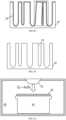
- Step S11providing a semiconductor structure, wherein the semiconductor structure comprises a substrate 20 and a plurality of etched structures 22 arranged on the surface area of the substrate 20, as shown in Fig. 2A .
- the etched structures 22may be any structures formed on the substrate 20 by means of a dry etching process.
- the etched structuresare trenches, and the number of the trenches arranged on the surface area of the substrate is more than one.
- the ratio of the depth H of the trench to the minimum width W of the trenchis greater than 8.
- the trenchesare arranged in parallel on the surface area of the substrate 20.
- the width D of the pattern line between two adjacent trenchesis less than 20nm.
- the etched structures 22may be trenches such as shallow trench isolation (STI) extending from the surface of the substrate 20 into the substrate 20 along the direction (i.e., the Y-axis direction in FIG. 2A ) perpendicular to the substrate 20.
- STIshallow trench isolation
- HARaspect ratio
- the method for processing a semiconductor structure provided in this embodimentis more effective in preventing the collapse or deformation of the trenches with higher aspect ratio during the cleaning process.
- FIG. 2Ashows five trenches arranged in parallel on the surface area of the substrate 20 (i.e., the X-axis direction in FIG. 2A ).
- the specific number of the trenchesmay be determined by the person skilled in the art according to actual needs.
- the aspect ratios of the plurality of trenchesmay be same or different.
- the term "a plurality of" in this specific embodimentmeans two or more.
- the step of providing a semiconductor structureincludes:
- cleaning the semiconductor structurecomprises the following specific steps:
- processing the semiconductor structure by means of the plasma ashing processcomprises the following specific steps: performing the ashing process on the surface of the semiconductor structure by means of plasmonized oxygen to remove the polymer residues generated after the trenches are formed by the etching.
- performing the ashing process on the surface of the semiconductor structure by means of the plasmonized oxygencomprises the following specific step: simultaneously introducing the plasmonized oxygen and a mixed gas composed of hydrogen and nitrogen, wherein the ratio of the flow of the oxygen to the flow of the mixed gas is 10:1.
- the volume ratio of the hydrogen in the mixed gas composed of the hydrogen and the nitrogenis 4%.
- the surface of the substrate 20has a mask layer, such as a first mask layer 211 covering the surface of the substrate 20 and a second mask layer 212 covering the surface of the first mask layer 211 in FIG. 2A .
- the mask layerhas a mask pattern. After the substrate 20 is etched by dry etching process or other etching processes along the mask pattern in the mask layer to form the trenches, some polymers (i.e., the polymer residues) may remain inside the trenches. Some by-products and pollutants may also be generated by the etching reaction between the etchant and the substrate 20.
- the polymer residuesare first removed by the plasma ashing process, and then the by-products and the pollutants are removed by wet cleaning process, to make sure the inside of the trenches and the surface of the substrate clear.
- the material of the first mask layer 211may be silicon oxide
- the material of the second mask layer 212may be silicon nitride.
- the flow rate of the oxygenis 5,000ml/min-30,000ml/min
- the flow rate of the mixed gas composed of the hydrogen and the nitrogen(the volume ratio of the hydrogen is 4%) is 500ml/min ⁇ 3,000ml/min
- the temperatureis 100°C ⁇ 500°C
- the durationis 10s ⁇ 120s
- the pressure in the processing chamberis of 200 mtorr ⁇ 5,000 mtorr
- the radio frequency (RF) poweris of 1,000 W ⁇ 10,000 W.
- the cleaning agentmay be diluted HF (DHF), wherein the volume ratio of the HF (49% HF liquid) to the deionized water is 1: (1 ⁇ 1000), the duration is 5s ⁇ 600s, the temperature is 15°C ⁇ 60°C, and the rotation speed of the support platform is 100rpm ⁇ 3,000rpm.
- DHFdiluted HF
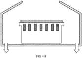
- the substrate 20 with the trenchesis placed onto the support platform 41 in the processing chamber 40 as shown in FIG. 4A .
- a spray head 42sprays the plasmonized oxygen to the substrate 20 at a flow rate of 13,000 ml/min, and simultaneously sprays the plasmonized mixed gas (the mixed gas is composed of the hydrogen and the nitrogen, and the volume ratio of the hydrogen is 4%) to the substrate at the flow rate of 1,300 ml/min, the temperature in the processing chamber 40 is maintained at 250°C, the pressure is 1,200mtorr, the RF power is 4,400W, and the duration is 21s.
- the DHF (1:200)is used as the cleaning agent, as shown in FIG. 4B .
- the cleaning agentis sprayed onto the surface of the substrate 20 through the spray head 42, meanwhile the support platform 41 rotates at the speed of 1,500 rpm, the temperature is room temperature, and the duration is 130s.
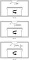
- Step S12forming a transition layer 24, the transition layer 24 at least covering the inner walls of the etched structures 22, where the transition layer 24 is configured to reduce a capillary force exerted by a fluid on the etched structures 22, and to serve as a sacrificial layer configured to repair a collapsed structure, as shown in FIG. 2C .
- forming a transition layer 24, the transition layer 24 at least covering the inner walls of the etched structures 22comprises the following specific step: oxidizing the semiconductor structure to form an oxide layer, the oxide layer at least covering the inner walls of the trenches, wherein the oxide layer is the transition layer 24.
- oxidizing the semiconductor structurecomprises the following specific step: processing the semiconductor structure by means of an oxidizing liquid, wherein the oxidizing liquid at least fills up the trenches, as shown in FIG. 2B .
- the oxidizing liquidis an ozone deionized aqueous solution (DIO 3 ) or a mixed solution (i.e., APM solution) composed of ammonia water and hydrogen peroxide solution.
- DIO 3ozone deionized aqueous solution
- APM solutiona mixed solution composed of ammonia water and hydrogen peroxide solution.
- processing the semiconductor structure by means of the oxidizing liquidcomprises the following step: spraying the oxidizing liquid to the surface of the semiconductor structure being spinning to rinse the semiconductor structure.
- the oxide layerhas a thickness of 2 ⁇ to 12 ⁇ .
- the ozone deionized aqueous solution or the APM solutionmay be sprayed to the substrate 20 through the spray head 42, while the support platform keeps spinning.
- the oxidizing liquidis the ozone deionized aqueous solution
- the flow rate of O 3 mixed into the deionized wateris 1L/min ⁇ 10L/min
- the flow rate of the ozone deionized aqueous solutionis 1L/min ⁇ 10L/min
- the process temperatureis 5 °C ⁇ 35 °C
- the process durationis 6s ⁇ 1,800s
- the rotation speed of the support platformis 100rpm ⁇ 1,200rpm
- the thickness of the oxide layer formedis 2 ⁇ 12 ⁇ .
- the oxidizing liquidis the APM solution
- the temperatureis 20°C ⁇ 65°C
- the durationis 10 s ⁇ 600 s
- the process conditionssuch as the flow rate of the APM solution and the rotation speed of the support platform may be the same as those needed when the ozone deionized aqueous solution is used as an oxidizing solution.
- the oxide layer formedhas 2 ⁇ 12 ⁇ of a thickness. The person skilled in the art may adjust the thickness of the generated transition layer 24 by adjusting the process conditions.
- the material of the transition layer 24is silicon dioxide. Due to the transition layer 24 formed in the semiconductor structure, the transition layer 24 can be prevented from serving as the interface layer between the silicon and the fluid in the subsequent semiconductor rinsing process, such that the resistance of the trenches to the tension of the fluid can be enhanced, i.e., the capillary force exerted by the fluid on the trenches can be reduced. In this way, the pattern structures such as the trenches may be protected.
- transition layer 24(such as the oxide layer) may also change the hydrophobicity of the semiconductor structure, thereby reducing the Van der Waals' force exerted by the silicon surface on the particulates, such that it is more advantageous to removing the particulates inside the etched structures such as the trenches.
- Step S13drying the semiconductor structure, as shown in FIG. 2D .
- drying the semiconductor structurecomprises the following specific step: processing the semiconductor structure by means of isopropanol at a preset temperature to remove the moisture on the surface area of the semiconductor structure.
- hot isopropanol(Hot-IPA) is used as a drying fluid.
- the Hot-IPAcan remove the moisture on the surface area of the semiconductor structure, and in another aspect, it can also help to further reduce the surface tension.
- the drying fluidis sprayed onto the surface of the semiconductor structure through the spray head 42, and at the same time, the nitrogen is introduced, as the purge gas, into the processing chamber to purge the isopropanol away through the exhaust port of the processing chamber. In this way, the semiconductor structure is dried.
- the flow rate of the isopropanolis 50ml/min ⁇ 500ml/min, the temperature is 40°C ⁇ 80°C, the duration is 10s ⁇ 600s, and the rotation speed of the support platform is 100 rpm ⁇ 4,000 rpm.
- the temperatureis preset at 40°C ⁇ 80°C, for example 60°C.
- Step S14removing the transition layer 24, as shown in FIG. 2F .
- removing the transition layer 24comprises the following specific step: removing the transition layer 24 by means of a mixed gas composed of hydrogen fluoride (99.999% HF gaseous) and ammonia gas as the etching gas.
- the substrate 20 and the transition layer 24 removed by the etching by means of the mixed gas composed of the hydrogen fluoride and the ammonia gas as the etching gashave a total thickness of 1nm to 10nm.
- the ratio of the flow of the hydrogen fluoride to the flow of the ammonia gasis (1 ⁇ 2):1.
- HF and NH 3are simultaneously introduced into the processing chamber, and the transition layer 24 is removed by means of a vapor etching method.
- the material of the transition layer 24is silicon dioxide
- the chemical reaction occurring in the process of etching the silicon dioxide by HF and NH 3is as shown in FIG. 2E .
- the exhaust gas produced in the reaction processis drawn away in time through the exhaust port at the bottom of the processing chamber, as shown by the arrows in FIG. 4E and FIG. 4F .
- a ratio of the flow of HF to the flow of NH 3is (1 ⁇ 2):1.
- the flow rate of HF and the NH 3is 10 sccm ⁇ 300 sccm (for example, 25sccm), the temperature is 20°C ⁇ 150°C (for example, 130°C) , and the duration is 1 s ⁇ 60 s, the pressure in the processing chamber is 1 mtorr ⁇ 5,000 mtorr and the temperature of the support platform is 20°C ⁇ 150°C (for example, 35°C).
- the transition layer 24is over-etched to fully remove the transition layer, such that the etched structures deformed in the drying process by using the isopropanol can be restored to the greatest extent.
- the thickness of the transition layer 24 etched awaymay be 1nm to 10 nm.
- the process of alternately and cyclically introducing NH 3 /HF and N 2may also be adopted.
- HF and NH 3are introduced in the first stage
- N 2is introduced in the second stage
- HF and NH 3are introduced in the third stage
- N 2is introduced in the fourth stage..., and so on alternately.
- the methodfurther comprises the following step: purging the semiconductor structure by means of a gas, as shown in FIG. 4G and FIG. 4H .
- a heater 43 inside the support platformis used to heat the substrate 20 to evaporate the products generated in the etching reaction.
- the nitrogenis introduced into the processing chamber and the processing chamber is continuously evacuated, such that the residues generated after the etching reaction are discharged from the processing chamber in time.
- the processing chamberis further purged by means of the nitrogen, as shown in FIG. 4G , until the support platform stops spinning, and the entire wet cleaning process is completed, as shown in FIG. 4H .
- the flow rate of the nitrogenis 200sccm ⁇ 10,000scem (for example, 2,000sccm).
- the temperature of the wet cleaningis 90°C ⁇ 250°C (for example, 95°C)
- the durationis 20s ⁇ 600s(for example, 120s)
- the pressure of the processing chamberis 200 mtorr ⁇ 10,000 mtorr (for example, 2,000mtorr).
- the probability of occurrence of collapse or deformation of the pattern after the cleaning processis less than 2%.
- FIGS 2A-2Fshow a method for processing a semiconductor structure where an etched structures is formed by a mask layer.
- the surface of the substrate 20may also have no mask layer.
- FIG. 3A-FIG. 3Eare schematic diagrams showing major technologies during processing another semiconductor structure according to embodiments of the present disclosure. That is, FIG. 3A-FIG. 3E illustrate schematic diagrams of processing the semiconductor structure having no mask layer on the surface of the substrate.
- the processing steps and the process conditions during the implementation of each of the processing stepsmay be the same as the conditions as shown in FIG. 2A to FIG. 2F and FIG. 4A to FIG. 4H .
- the transition layer configured to reduce the capillary force exerted by the fluid on the etched structuresis formed on the inner walls of the etched structures, such that the probability of collapse or deformation of the etched structures is reduced in the subsequent process of drying the etched structures. Furthermore, the transition layer covering the inner walls of the etched structures is removed after being dried, and the attraction between the patterns of the etched structures is broken, such that the etched structures deformed in the previous drying process is restored to its original state, thereby further reducing the probability of collapse or deformation of the etched structures. In this way, the performance of the semiconductor structure is improved, and the productivity and the yield of the semiconductor devices are increased.
Landscapes
- Engineering & Computer Science (AREA)
- Physics & Mathematics (AREA)
- Manufacturing & Machinery (AREA)
- Microelectronics & Electronic Packaging (AREA)
- General Physics & Mathematics (AREA)
- Computer Hardware Design (AREA)
- Condensed Matter Physics & Semiconductors (AREA)
- Power Engineering (AREA)
- Chemical & Material Sciences (AREA)
- Plasma & Fusion (AREA)
- Chemical Kinetics & Catalysis (AREA)
- General Chemical & Material Sciences (AREA)
- Inorganic Chemistry (AREA)
- Cleaning Or Drying Semiconductors (AREA)
- Drying Of Semiconductors (AREA)
Description
- This application claims priority to
Chinese Patent Application No. 202010166572.2, titled "METHOD FOR PROCESSING SEMICONDUCTOR STRUCTURE" and filed on March 11, 2020 - The present disclosure relates to the field of semiconductor production technology, and more particularly, to a method for processing a semiconductor structure.
- With the rapid development of the semiconductor industry in recent years, high-aspect-ratio (HAR) nanostructures have been widely used in various fields. As nanometer devices are increasingly pursued in technology, the feature size of chips continues to shrink in a production process, and the entire semiconductor production technology is still developing towards further miniaturization of critical dimensions.
- After patterns such as trenches are etched in semiconductor structures such as a Dynamic Random Access Memory (DRAM), steps of wet cleaning and drying are generally required to remove the byproduct generated in the etching process or the residual polymers generated after the etching process. However, in the processes of the wet cleaning and the drying, a capillary action may cause the collapse or deformation of the patterns. The smaller the sizes of the trenches formed by etching are, the greater the tension of the fluid likely appearing in the semiconductor structure is. There are three factors generally causing the collapse of the patterns: Laplace pressure; adhesive force; and electrostatic force, Van der Waals' force, and hydrogen-bond interaction. In an advanced DRAM production process, the collapse of the patterns may seriously affect the yield and productivity rate of the chips, and increasingly becomes a key factor in determining the success or failure of the DRAM production process. Particularly, a HAR Shallow Trench Isolation (STI) structure has more severe collapse or deformation of the patterns due to the capillary action in the wet cleaning. Therefore, it is of vital importance to eliminate or reduce the risk of the collapse of the pattern in the production of semiconductor devices such as the DARM.
- However, in the more advanced DRAM production process, with the size of the structure becoming smaller and requirement for HAR, a great challenge is posed to the stability of the liquid environment during cleaning. Therefore, the surface effect of the cleaning liquid becomes a major factor affecting production quality. In some embodiments, the wet cleaning may cause the collapse of the patterns due to the capillary action on the pattern structures. The occurrence of the collapse of the patterns may be reduced by means of surface finishing of the HAR structure. However, this treatment method may lead to other negative effects, such as the super-hydrophobic effect of the HAR structure. This super-hydrophobic effect may prevent the aqueous solution from penetrating into the structure, resulting in a decrease in the effect of wet cleaning. In addition, taking the STI production as an example, a surface finishing agent is added after the wet cleaning before the drying process, which can effectively prevent the occurrence of pattern collapse. However, the surface finishing agent may remain at the bottom of the STI structure, which may cause abnormalities of the semiconductor devices.
- D1 (
US2016172433A1 ) discloses a surface treatment method for a semiconductor device having capacitor patterns, comprising: providing a substrate where a plurality of projected capacitor patterns are formed in a mold insulation layer; removing the mold insulation layer by using a wet etch solution; rinsing the substrate from which the mold insulation layer is removed with deionized water; treating the substrate with an SC-1 (NHOH+HO+OH) solution; rinsing the treated substrate with deionized water; forming a hydrophobic coating layer on a surface of each of plurality of the projected capacitor patterns; rinsing the substrate where the hydrophobic coating layer is formed with deionized water; and drying the substrate, wherein the hydrophobic coating layer is formed using a coating agent that includes phosphate having more than one hydrocarbon group, phosphonate having more than one hydrocarbon group, or a mixture thereof. - D2 (
EP2490249A1 ) discloses a chemical solution for forming a water-repellent protective film on a wafer, which is a chemical solution containing a water-repellent-protective-film-forming agent for forming the water-repellent protective film, at the time of cleaning the wafer which has a finely uneven pattern at its surface and contains at least at a part of a surface of a recessed portion of the uneven pattern at least one kind of matter selected from the group consisting of titanium, titanium nitride, tungsten, aluminum, copper, tin, tantalum nitride, ruthenium and silicon, at least on the surface of the recessed portion, the chemical solution being characterized in that the water-repellent-protective-film-forming agent is a water-insoluble surfactant. - D3 (
US2011189858A1 ) discloses a method of processing a wafer used in fabricating semiconductor devices, said method comprising: forming high aspect ratio features in a silicon based layer on the wafer; making sidewalls of the features more hydrophobic; performing wet processing of the wafer; and subsequently drying the wafer. - D4 (
US2019189455A1 ) discloses a method for forming a semiconductor device, comprising: forming a silicon-hydrogen (Si-H) terminated surface on a silicon structure that includes patterned features by exposing the silicon structure to a hydrogen fluoride (HF) containing solution; removing the HF containing solution via a deionized (DI) water rinse; forming a solvent on the Si-H terminated surface on the silicon structure; and performing a surface modification via hydrosilylation by exposing the Si-H terminated surface to an alkene and/or an alkyne. - D5 (
US2017186620A1 ) discloses a substrate processing method comprising: a liquid processing process of supplying a processing liquid to a substrate having a surface on which a pattern having a plurality of convex portions is formed; a drying process of removing the processing liquid existing on the surface of the substrate to dry the substrate; and a separating process of separating a sticking portion between adjacent ones of the convex portions after the drying process. - D6 (
EP1132951A1 ) discloses an improved pre-gate cleaning technique that results in a smoother wafer surface. - D7 (
US20160086845A1 ) discloses a method for processing an inner wall surface of a micro vacancy. - D8 (
US20180076022A1 ) discloses a method of treating a semiconductor substrate. - D9 (
CN106229288A ) discloses a method for preparing active regions. - Therefore, it is a technical problem to be solved urgently at present how to reduce the occurrence of pattern collapse or deformation in the wet cleaning process of the semiconductor structures to improve the performance of the semiconductor structures and increase the yield of the semiconductor devices.
- The present disclosure provides a method for processing a semiconductor structure. This method is used for solving the problem of pattern collapse or deformation prone to occur in a cleaning process of the semiconductor structure, to improve the performance of the semiconductor structure and increase the yield of the semiconductor devices.
- To solve the above problem, the present disclosure provides a method for processing a semiconductor structure, and the invention is set out in the appended set of claims. By using the method for processing a semiconductor structure provided by the present disclosure, a transition layer configured to reduce the capillary force exerted by a fluid on the etched structures is formed on the inner walls of the etched structures such that the probability of collapse or deformation of the etched structures is reduced in the subsequent process of drying the etched structures. Furthermore, the transition layer covering the inner walls of the etched structures is removed after being dried, so the attraction force between the patterns of the etched structures is broken such that the etched structures deformed in the previous drying process is restored to its original state, thereby further reducing the probability of collapse or deformation of the etched structures, improving the performance of the semiconductor structure, and increasing the productivity and the yield of the semiconductor devices.
FIG. 1 is a flowchart of a method for processing a semiconductor structure according to embodiments of the present disclosure;FIG. 2A-FIG. 2F are schematic diagrams showing major technologies during processing a semiconductor structure according to embodiments of the present disclosure;FIG. 3A-FIG. 3E are schematic diagrams showing major technologies during processing another semiconductor structure according to embodiments of the present disclosure; andFIG. 4A-FIG. 4H are schematic sectional views of a processing chamber during processing a semiconductor structure according to embodiments of the present disclosure.- A specific embodiment of a method for processing a semiconductor structure provided by the present disclosure is described in detail below with reference to the accompanying drawings.
- This specific embodiment provides a method for processing a semiconductor structure.
FIG. 1 is a flowchart of the method for processing a semiconductor structure according to this specific embodiment of the present disclosure.FIG. 2A-FIG. 2F are schematic diagrams showing major technologies during processing a semiconductor structure according to this specific embodiment of the present disclosure.FIG. 4A-FIG. 4H are schematic sectional views of a processing chambers during processing a semiconductor structure according to this specific embodiment of the present disclosure. As shown inFIG. 1 , -FIG. 2AFIG. 2F , andFIG. 4A-FIG. 4H , the method for processing a semiconductor structure provided by this specific embodiment includes following steps. - Step S11, providing a semiconductor structure, wherein the semiconductor structure comprises a
substrate 20 and a plurality ofetched structures 22 arranged on the surface area of thesubstrate 20, as shown inFig. 2A . - In this specific embodiment, the
etched structures 22 may be any structures formed on thesubstrate 20 by means of a dry etching process. In some embodiments, the etched structures are trenches, and the number of the trenches arranged on the surface area of the substrate is more than one. - The ratio of the depth H of the trench to the minimum width W of the trench is greater than 8.
- In some embodiments, the trenches are arranged in parallel on the surface area of the
substrate 20. - The width D of the pattern line between two adjacent trenches is less than 20nm.
- In some embodiments, the
etched structures 22 may be trenches such as shallow trench isolation (STI) extending from the surface of thesubstrate 20 into thesubstrate 20 along the direction (i.e., the Y-axis direction inFIG. 2A ) perpendicular to thesubstrate 20. In semiconductor production processes, trenches with higher aspect ratio (HAR) are more likely to collapse or deform during the cleaning process. The method for processing a semiconductor structure provided in this embodiment is more effective in preventing the collapse or deformation of the trenches with higher aspect ratio during the cleaning process.FIG. 2A shows five trenches arranged in parallel on the surface area of the substrate 20 (i.e., the X-axis direction inFIG. 2A ). In practical use, the specific number of the trenches may be determined by the person skilled in the art according to actual needs. The aspect ratios of the plurality of trenches may be same or different. The term "a plurality of" in this specific embodiment means two or more. - In some embodiments, the step of providing a semiconductor structure includes:
- providing a
substrate 20; - etching the
substrate 20 to form the plurality of trenches on the surface area of thesubstrate 20, the bottoms of the trenches extending into thesubstrate 20 to form the semiconductor structure; and - cleaning the semiconductor structure to remove the impurities after forming the trenches by etching.
- In some embodiments, cleaning the semiconductor structure comprises the following specific steps:
- processing the semiconductor structure by means of a plasma ashing process to remove the polymer residues after forming the trenches by etching; and
- processing the semiconductor structure by means of a wet cleaning process to remove the by-products and the pollutants generated after the etching process and the ashing process.
- In some embodiments, processing the semiconductor structure by means of the plasma ashing process comprises the following specific steps:
performing the ashing process on the surface of the semiconductor structure by means of plasmonized oxygen to remove the polymer residues generated after the trenches are formed by the etching. - In some embodiments, performing the ashing process on the surface of the semiconductor structure by means of the plasmonized oxygen comprises the following specific step:
simultaneously introducing the plasmonized oxygen and a mixed gas composed of hydrogen and nitrogen, wherein the ratio of the flow of the oxygen to the flow of the mixed gas is 10:1. The volume ratio of the hydrogen in the mixed gas composed of the hydrogen and the nitrogen is 4%. - In some embodiments, the surface of the
substrate 20 has a mask layer, such as afirst mask layer 211 covering the surface of thesubstrate 20 and asecond mask layer 212 covering the surface of thefirst mask layer 211 inFIG. 2A . The mask layer has a mask pattern. After thesubstrate 20 is etched by dry etching process or other etching processes along the mask pattern in the mask layer to form the trenches, some polymers (i.e., the polymer residues) may remain inside the trenches. Some by-products and pollutants may also be generated by the etching reaction between the etchant and thesubstrate 20. To avoid causing adverse effects on subsequent processes, in this specific embodiment, after etching the trenches, the polymer residues are first removed by the plasma ashing process, and then the by-products and the pollutants are removed by wet cleaning process, to make sure the inside of the trenches and the surface of the substrate clear. The material of thefirst mask layer 211 may be silicon oxide, and the material of thesecond mask layer 212 may be silicon nitride. - In the plasma ashing process, the flow rate of the oxygen is 5,000ml/min-30,000ml/min, the flow rate of the mixed gas composed of the hydrogen and the nitrogen (the volume ratio of the hydrogen is 4%) is 500ml/min~3,000ml/min, the temperature is 100°C~500°C, the duration is 10s~120s, the pressure in the processing chamber is of 200 mtorr~5,000 mtorr, and the radio frequency (RF) power is of 1,000 W~10,000 W. In wet cleaning process, the cleaning agent may be diluted HF (DHF), wherein the volume ratio of the HF (49% HF liquid) to the deionized water is 1: (1~1000), the duration is 5s~600s, the temperature is 15°C~60°C, and the rotation speed of the support platform is 100rpm~3,000rpm.
- For example, after the trenches are etched, the
substrate 20 with the trenches is placed onto thesupport platform 41 in theprocessing chamber 40 as shown inFIG. 4A . In the plasma ashing process, aspray head 42 sprays the plasmonized oxygen to thesubstrate 20 at a flow rate of 13,000 ml/min, and simultaneously sprays the plasmonized mixed gas (the mixed gas is composed of the hydrogen and the nitrogen, and the volume ratio of the hydrogen is 4%) to the substrate at the flow rate of 1,300 ml/min, the temperature in theprocessing chamber 40 is maintained at 250°C, the pressure is 1,200mtorr, the RF power is 4,400W, and the duration is 21s. After the plasma ashing process is completed, in wet cleaning process, the DHF (1:200) is used as the cleaning agent, as shown inFIG. 4B . The cleaning agent is sprayed onto the surface of thesubstrate 20 through thespray head 42, meanwhile thesupport platform 41 rotates at the speed of 1,500 rpm, the temperature is room temperature, and the duration is 130s. - Step S12, forming a
transition layer 24, thetransition layer 24 at least covering the inner walls of the etchedstructures 22, where thetransition layer 24 is configured to reduce a capillary force exerted by a fluid on theetched structures 22, and to serve as a sacrificial layer configured to repair a collapsed structure, as shown inFIG. 2C . - According to the invention, forming a
transition layer 24, thetransition layer 24 at least covering the inner walls of the etchedstructures 22 comprises the following specific step:
oxidizing the semiconductor structure to form an oxide layer, the oxide layer at least covering the inner walls of the trenches, wherein the oxide layer is thetransition layer 24. - In some embodiments, oxidizing the semiconductor structure comprises the following specific step:
processing the semiconductor structure by means of an oxidizing liquid, wherein the oxidizing liquid at least fills up the trenches, as shown inFIG. 2B . - The oxidizing liquid is an ozone deionized aqueous solution (DIO3) or a mixed solution (i.e., APM solution) composed of ammonia water and hydrogen peroxide solution.
- In some embodiments, processing the semiconductor structure by means of the oxidizing liquid comprises the following step:
spraying the oxidizing liquid to the surface of the semiconductor structure being spinning to rinse the semiconductor structure. - In some embodiments, the oxide layer has a thickness of 2Å to 12Å.
- In some embodiments, after the semiconductor structure is cleaned, as shown in
FIG. 4C , the ozone deionized aqueous solution or the APM solution may be sprayed to thesubstrate 20 through thespray head 42, while the support platform keeps spinning. For example, when the oxidizing liquid is the ozone deionized aqueous solution, the flow rate of O3 mixed into the deionized water is 1L/min~10L/min, the flow rate of the ozone deionized aqueous solution is 1L/min~10L/min, the process temperature is 5 °C~35 °C, the process duration is 6s~1,800s, the rotation speed of the support platform is 100rpm~1,200rpm, and the thickness of the oxide layer formed is 2Å~12Å. When the oxidizing liquid is the APM solution, the volume ratio of NH4OH, H2O2 and H2O in the APM solution is NH4OH:H2O2:H2O=1:(1~10):(10-200)(as an example: NH4OH:H2O2:H2O=1:7:58), the temperature is 20°C~65°C, the duration is 10 s~600 s, the process conditions such as the flow rate of the APM solution and the rotation speed of the support platform may be the same as those needed when the ozone deionized aqueous solution is used as an oxidizing solution. The oxide layer formed has 2Å~12Å of a thickness. The person skilled in the art may adjust the thickness of the generatedtransition layer 24 by adjusting the process conditions. - When the material of the
substrate 20 is silicon, the material of thetransition layer 24 is silicon dioxide. Due to thetransition layer 24 formed in the semiconductor structure, thetransition layer 24 can be prevented from serving as the interface layer between the silicon and the fluid in the subsequent semiconductor rinsing process, such that the resistance of the trenches to the tension of the fluid can be enhanced, i.e., the capillary force exerted by the fluid on the trenches can be reduced. In this way, the pattern structures such as the trenches may be protected. Additionally, the transition layer 24 (such as the oxide layer) may also change the hydrophobicity of the semiconductor structure, thereby reducing the Van der Waals' force exerted by the silicon surface on the particulates, such that it is more advantageous to removing the particulates inside the etched structures such as the trenches. - Step S13, drying the semiconductor structure, as shown in
FIG. 2D . - In some embodiments, drying the semiconductor structure comprises the following specific step:
processing the semiconductor structure by means of isopropanol at a preset temperature to remove the moisture on the surface area of the semiconductor structure. - In some embodiments, as shown in
FIG. 4D , hot isopropanol (Hot-IPA) is used as a drying fluid. In one aspect, the Hot-IPA can remove the moisture on the surface area of the semiconductor structure, and in another aspect, it can also help to further reduce the surface tension. The drying fluid is sprayed onto the surface of the semiconductor structure through thespray head 42, and at the same time, the nitrogen is introduced, as the purge gas, into the processing chamber to purge the isopropanol away through the exhaust port of the processing chamber. In this way, the semiconductor structure is dried. The flow rate of the isopropanol is 50ml/min~500ml/min, the temperature is 40°C~80°C, the duration is 10s~600s, and the rotation speed of the support platform is 100 rpm~4,000 rpm. The temperature is preset at 40°C~80°C, for example 60°C. - Step S14, removing the
transition layer 24, as shown inFIG. 2F . - In the drying process, due to the effect of the surface energy of the membrane layer on the surface of the wafer, electrostatic friction may be released and/or the attraction between molecules may be applied, and the top of the etched structure is more fragile than the bottom thereof, so the etched structures is prone to tilt at the top due to the aforementioned forces, as shown in the dashed box in
FIG. 2D . However, within the elastic limit, after thetransition layer 24 is removed, the attraction between the etched structures is broken, and the etched patterns may bounce off thanks to restoring force to restore to its original state, as shown inFIG. 2F . - According to the invention, removing the
transition layer 24 comprises the following specific step:
removing thetransition layer 24 by means of a mixed gas composed of hydrogen fluoride (99.999% HF gaseous) and ammonia gas as the etching gas. - In some embodiments, the
substrate 20 and thetransition layer 24 removed by the etching by means of the mixed gas composed of the hydrogen fluoride and the ammonia gas as the etching gas have a total thickness of 1nm to 10nm. - According to the invention, the ratio of the flow of the hydrogen fluoride to the flow of the ammonia gas is (1~2):1.
- In some embodiments, as shown in
FIG. 4E and 4F , HF and NH3 are simultaneously introduced into the processing chamber, and thetransition layer 24 is removed by means of a vapor etching method. Taking as an example where the material of thetransition layer 24 is silicon dioxide, the chemical reaction occurring in the process of etching the silicon dioxide by HF and NH3 is as shown inFIG. 2E . In the process of removing the transition layer, the exhaust gas produced in the reaction process is drawn away in time through the exhaust port at the bottom of the processing chamber, as shown by the arrows inFIG. 4E and FIG. 4F . According to the invention, in the process of etching thetransition layer 24, a ratio of the flow of HF to the flow of NH3 is (1~2):1. The flow rate of HF and the NH3 is 10 sccm~300 sccm (for example, 25sccm), the temperature is 20°C~150°C (for example, 130°C) , and the duration is 1 s~60 s, the pressure in the processing chamber is 1 mtorr~5,000 mtorr and the temperature of the support platform is 20°C~150°C (for example, 35°C). In this step, thetransition layer 24 is over-etched to fully remove the transition layer, such that the etched structures deformed in the drying process by using the isopropanol can be restored to the greatest extent. The thickness of thetransition layer 24 etched away may be 1nm to 10 nm. In the process of removing thetransition layer 24 in this step, the process of alternately and cyclically introducing NH3/HF and N2 may also be adopted. For example, HF and NH3 are introduced in the first stage, N2 is introduced in the second stage, HF and NH3 are introduced in the third stage, N2 is introduced in the fourth stage..., and so on alternately. - In some embodiments, after removing the
transition layer 24, the method further comprises the following step:
purging the semiconductor structure by means of a gas, as shown inFIG. 4G andFIG. 4H . - In some embodiments, after the process of etching the
transition layer 24 is completed, in one aspect, aheater 43 inside the support platform is used to heat thesubstrate 20 to evaporate the products generated in the etching reaction. In another aspect, the nitrogen is introduced into the processing chamber and the processing chamber is continuously evacuated, such that the residues generated after the etching reaction are discharged from the processing chamber in time. Finally, the processing chamber is further purged by means of the nitrogen, as shown inFIG. 4G , until the support platform stops spinning, and the entire wet cleaning process is completed, as shown inFIG. 4H . In the process of gas purging the semiconductor structure by means of the gas, the flow rate of the nitrogen is 200sccm~10,000scem (for example, 2,000sccm). The temperature of the wet cleaning is 90°C~250°C (for example, 95°C), the duration is 20s~600s(for example, 120s), the pressure of the processing chamber is 200 mtorr~10,000 mtorr (for example, 2,000mtorr). - By using the method for processing a semiconductor structure provided in this embodiment, when the depth H of the trench is 300nm or 310nm, the probability of occurrence of collapse or deformation of the pattern after the cleaning process is less than 2%.
FIGS 2A-2F show a method for processing a semiconductor structure where an etched structures is formed by a mask layer. In other specific embodiments, during processing, the surface of thesubstrate 20 may also have no mask layer.FIG. 3A-FIG. 3E are schematic diagrams showing major technologies during processing another semiconductor structure according to embodiments of the present disclosure. That is,FIG. 3A-FIG. 3E illustrate schematic diagrams of processing the semiconductor structure having no mask layer on the surface of the substrate. The processing steps and the process conditions during the implementation of each of the processing steps may be the same as the conditions as shown inFIG. 2A to FIG. 2F andFIG. 4A to FIG. 4H .- By using the method for processing a semiconductor structure provided by this embodiment of the present disclosure, the transition layer configured to reduce the capillary force exerted by the fluid on the etched structures is formed on the inner walls of the etched structures, such that the probability of collapse or deformation of the etched structures is reduced in the subsequent process of drying the etched structures. Furthermore, the transition layer covering the inner walls of the etched structures is removed after being dried, and the attraction between the patterns of the etched structures is broken, such that the etched structures deformed in the previous drying process is restored to its original state, thereby further reducing the probability of collapse or deformation of the etched structures. In this way, the performance of the semiconductor structure is improved, and the productivity and the yield of the semiconductor devices are increased.
Claims (12)
- A method for processing a semiconductor structure comprising:providing a semiconductor structure, the semiconductor structure comprising a substrate (20) and a plurality of etched structures (22) arranged on a surface area of the substrate (20) (S11);forming a transition layer (24), the transition layer (24) at least covering inner walls of the plurality of etched structures (22), the transition layer (24) being configured to reduce a capillary force exerted by a fluid on the etched structures (22) and to serve as a sacrificial layer configured to repair a collapsed structure (S12);wherein the forming a transition layer (24), the transition layer (24) at least covering inner walls of the plurality of etched structures (22) comprises:oxidizing the semiconductor structure to form an oxide layer, the oxide layer at least covering inner walls of the trenches, the oxide layer being the transition layer (24);drying the semiconductor structure (S13); andremoving the transition layer (24), after drying the semiconductor structure (S14);wherein the removing the transition layer (24) comprises:removing the transition layer (24) by means of a mixed gas comprising hydrogen fluoride and ammonia gas as etching gas;wherein flow ratio of the hydrogen fluoride to the ammonia gas is (1~2):1; flow rate of the hydrogen fluoride and the ammonia gas is 10 sccm~300 sccm, temperature is 20°C~150°C, and duration is 1 s~60 s, pressure in a processing chamber is 1 mtorr~5,000 mtorr, and temperature of a support platform is 20°C~150°C.
- The method for processing a semiconductor structure according to claim 1, wherein the plurality of etched structures (22) are trenches, and number of the trenches arranged on the surface area of the substrate (20) is more than one; and
wherein ratio of depth of each of the trenches to minimum width of the trenches is greater than 8. - The method for processing a semiconductor structure according to claim 2, wherein the trenches are arranged in parallel on the surface area of the substrate (20); and
width of pattern line between two adjacent trenches is less than 20 nm. - The method for processing a semiconductor structure according to claim 2, wherein the providing a semiconductor structure comprises:providing the substrate (20);etching the substrate (20) to form the trenches on the surface area of the substrate (20), bottoms of the trenches extending into the substrate (20) to form the semiconductor structure; andcleaning the semiconductor structure to remove impurities generated after the trenches are formed by the etching.
- The method for processing a semiconductor structure according to claim 4, wherein the cleaning the semiconductor structure comprises:processing the semiconductor structure by means of a plasma ashing process to remove polymer residues generated after the trenches are formed by the etching; andprocessing the semiconductor structure by means of a wet cleaning process to remove by-products and pollutants generated after the etching process and the plasma ashing process.
- The method for processing a semiconductor structure according to claim 5, wherein the processing the semiconductor structure by means of a plasma ashing process comprises:
performing the plasma ashing process on a surface of the semiconductor structure by means of plasmonized oxygen to remove the polymer residues generated after the trenches are formed by the etching. - The method for processing a semiconductor structure according to claim 1, wherein the oxidizing the semiconductor structure comprises:
processing the semiconductor structure by means of an oxidizing liquid, the oxidizing liquid at least filling up the trenches, and the oxidizing liquid being an ozone deionized aqueous solution or a mixed solution of ammonia water and hydrogen peroxide. - The method for processing a semiconductor structure according to claim 7, wherein the processing the semiconductor structure by means of an oxidizing liquid comprises:
spraying the oxidizing liquid to a surface of the semiconductor structure being spinning to rinse the semiconductor structure. - The method for processing a semiconductor structure according to claim 1, wherein the oxide layer has a thickness of 2Å to 12Å.
- The method for processing a semiconductor structure according to claim 1, wherein a total thickness of the substrate (20) and the transition layer (24) removed by the etching by means of the mixed gas comprising the hydrogen fluoride and the ammonia gas as the etching gas is 1nm to 10nm.
- The method for processing a semiconductor structure according to claim 2, wherein the drying the semiconductor structure comprises:
processing the semiconductor structure by means of isopropanol at a preset temperature to remove moisture on a surface area of the semiconductor structure. - The method for processing a semiconductor structure according to claim 1, after the removing the transition layer (24), the method further comprises:
purging the semiconductor structure by means of a gas.
Applications Claiming Priority (2)
| Application Number | Priority Date | Filing Date | Title |
|---|---|---|---|
| CN202010166572.2ACN113394074A (en) | 2020-03-11 | 2020-03-11 | Method for processing semiconductor structure |
| PCT/CN2021/079971WO2021180121A1 (en) | 2020-03-11 | 2021-03-10 | Method for processing semiconductor structure |
Publications (3)
| Publication Number | Publication Date |
|---|---|
| EP3951837A1 EP3951837A1 (en) | 2022-02-09 |
| EP3951837A4 EP3951837A4 (en) | 2022-07-20 |
| EP3951837B1true EP3951837B1 (en) | 2025-02-12 |
Family
ID=77615338
Family Applications (1)
| Application Number | Title | Priority Date | Filing Date |
|---|---|---|---|
| EP21768606.2AActiveEP3951837B1 (en) | 2020-03-11 | 2021-03-10 | Method for processing semiconductor structure |
Country Status (6)
| Country | Link |
|---|---|
| US (1) | US20210335594A1 (en) |
| EP (1) | EP3951837B1 (en) |
| JP (1) | JP2023508553A (en) |
| KR (1) | KR102717795B1 (en) |
| CN (1) | CN113394074A (en) |
| WO (1) | WO2021180121A1 (en) |
Families Citing this family (4)
| Publication number | Priority date | Publication date | Assignee | Title |
|---|---|---|---|---|
| CN113495675B (en) | 2020-04-01 | 2023-08-11 | 长鑫存储技术有限公司 | Read-write method and memory device |
| CN113889405B (en) | 2020-07-02 | 2024-07-05 | 长鑫存储技术有限公司 | Method for processing and forming semiconductor structure |
| JP7411818B2 (en) | 2020-07-02 | 2024-01-11 | チャンシン メモリー テクノロジーズ インコーポレイテッド | Methods for processing and forming semiconductor structures |
| EP4539095A1 (en)* | 2023-10-13 | 2025-04-16 | Imec VZW | Fin-type and complementary-type field-effect transistors |
Citations (5)
| Publication number | Priority date | Publication date | Assignee | Title |
|---|---|---|---|---|
| EP1132951A1 (en)* | 2000-03-10 | 2001-09-12 | Lucent Technologies Inc. | Process of cleaning silicon prior to formation of the gate oxide |
| US20050022839A1 (en)* | 1999-10-20 | 2005-02-03 | Savas Stephen E. | Systems and methods for photoresist strip and residue treatment in integrated circuit manufacturing |
| US20160086845A1 (en)* | 2013-05-15 | 2016-03-24 | Tohoku University | A method for processing an inner wall surface of a micro vacancy |
| CN106229288A (en)* | 2016-07-27 | 2016-12-14 | 上海华虹宏力半导体制造有限公司 | active area preparation method |
| US20180076022A1 (en)* | 2016-09-13 | 2018-03-15 | SK Hynix Inc. | Method of treating semiconductor substrate |
Family Cites Families (24)
| Publication number | Priority date | Publication date | Assignee | Title |
|---|---|---|---|---|
| US5838055A (en)* | 1997-05-29 | 1998-11-17 | International Business Machines Corporation | Trench sidewall patterned by vapor phase etching |
| US6258663B1 (en)* | 1998-05-01 | 2001-07-10 | Vanguard International Semiconductor Corporation | Method for forming storage node |
| KR100505419B1 (en)* | 2003-04-23 | 2005-08-04 | 주식회사 하이닉스반도체 | Method for manufacturing isolation layer in semiconductor device |
| US20040235299A1 (en)* | 2003-05-22 | 2004-11-25 | Axcelis Technologies, Inc. | Plasma ashing apparatus and endpoint detection process |
| JP5229711B2 (en)* | 2006-12-25 | 2013-07-03 | 国立大学法人名古屋大学 | Pattern forming method and semiconductor device manufacturing method |
| US7838425B2 (en)* | 2008-06-16 | 2010-11-23 | Kabushiki Kaisha Toshiba | Method of treating surface of semiconductor substrate |
| JP5413016B2 (en)* | 2008-07-31 | 2014-02-12 | 東京エレクトロン株式会社 | Substrate cleaning method, substrate cleaning apparatus and storage medium |
| US20100122711A1 (en)* | 2008-11-14 | 2010-05-20 | Advanced Micro Devices, Inc. | wet clean method for semiconductor device fabrication processes |
| JP4743340B1 (en)* | 2009-10-28 | 2011-08-10 | セントラル硝子株式会社 | Chemical solution for protective film formation |
| JP5404361B2 (en)* | 2009-12-11 | 2014-01-29 | 株式会社東芝 | Semiconductor substrate surface treatment apparatus and method |
| JP5424848B2 (en)* | 2009-12-15 | 2014-02-26 | 株式会社東芝 | Semiconductor substrate surface treatment apparatus and method |
| US8440573B2 (en)* | 2010-01-26 | 2013-05-14 | Lam Research Corporation | Method and apparatus for pattern collapse free wet processing of semiconductor devices |
| US8617993B2 (en)* | 2010-02-01 | 2013-12-31 | Lam Research Corporation | Method of reducing pattern collapse in high aspect ratio nanostructures |
| JP5678720B2 (en)* | 2011-02-25 | 2015-03-04 | セントラル硝子株式会社 | Wafer cleaning method |
| SG10201506742RA (en)* | 2010-08-27 | 2015-10-29 | Entegris Inc | Method for preventing the collapse of high aspect ratio structures during drying |
| JP2012084789A (en)* | 2010-10-14 | 2012-04-26 | Toshiba Corp | Method for manufacturing semiconductor device and semiconductor manufacturing equipment |
| US20120187522A1 (en)* | 2011-01-20 | 2012-07-26 | International Business Machines Corporation | Structure and method for reduction of vt-w effect in high-k metal gate devices |
| KR102084073B1 (en)* | 2012-12-21 | 2020-03-04 | 에스케이하이닉스 주식회사 | Method for surface treatment of semiconductor device |
| US9520459B2 (en)* | 2012-12-21 | 2016-12-13 | SK Hynix Inc. | Surface treatment method for semiconductor device |
| JP6466315B2 (en)* | 2015-12-25 | 2019-02-06 | 東京エレクトロン株式会社 | Substrate processing method and substrate processing system |
| JP6966698B2 (en)* | 2017-02-20 | 2021-11-17 | セントラル硝子株式会社 | Chemical solution for forming a water-repellent protective film |
| US10475656B2 (en)* | 2017-12-19 | 2019-11-12 | Micron Technology, Inc. | Hydrosilylation in semiconductor processing |
| US10497558B2 (en)* | 2018-02-26 | 2019-12-03 | Micron Technology, Inc. | Using sacrificial polymer materials in semiconductor processing |
| JP7077184B2 (en)* | 2018-08-30 | 2022-05-30 | キオクシア株式会社 | Substrate processing method and semiconductor device manufacturing method |
- 2020
- 2020-03-11CNCN202010166572.2Apatent/CN113394074A/enactivePending
- 2021
- 2021-03-10KRKR1020227022239Apatent/KR102717795B1/enactiveActive
- 2021-03-10WOPCT/CN2021/079971patent/WO2021180121A1/ennot_activeCeased
- 2021-03-10EPEP21768606.2Apatent/EP3951837B1/enactiveActive
- 2021-03-10JPJP2022540435Apatent/JP2023508553A/enactivePending
- 2021-07-08USUS17/371,027patent/US20210335594A1/ennot_activeAbandoned
Patent Citations (5)
| Publication number | Priority date | Publication date | Assignee | Title |
|---|---|---|---|---|
| US20050022839A1 (en)* | 1999-10-20 | 2005-02-03 | Savas Stephen E. | Systems and methods for photoresist strip and residue treatment in integrated circuit manufacturing |
| EP1132951A1 (en)* | 2000-03-10 | 2001-09-12 | Lucent Technologies Inc. | Process of cleaning silicon prior to formation of the gate oxide |
| US20160086845A1 (en)* | 2013-05-15 | 2016-03-24 | Tohoku University | A method for processing an inner wall surface of a micro vacancy |
| CN106229288A (en)* | 2016-07-27 | 2016-12-14 | 上海华虹宏力半导体制造有限公司 | active area preparation method |
| US20180076022A1 (en)* | 2016-09-13 | 2018-03-15 | SK Hynix Inc. | Method of treating semiconductor substrate |
Also Published As
| Publication number | Publication date |
|---|---|
| KR20220107040A (en) | 2022-08-01 |
| US20210335594A1 (en) | 2021-10-28 |
| EP3951837A4 (en) | 2022-07-20 |
| KR102717795B1 (en) | 2024-10-15 |
| CN113394074A (en) | 2021-09-14 |
| EP3951837A1 (en) | 2022-02-09 |
| JP2023508553A (en) | 2023-03-02 |
| WO2021180121A1 (en) | 2021-09-16 |
Similar Documents
| Publication | Publication Date | Title |
|---|---|---|
| EP3951837B1 (en) | Method for processing semiconductor structure | |
| US10600639B2 (en) | SiN spacer profile patterning | |
| US10062575B2 (en) | Poly directional etch by oxidation | |
| TWI579892B (en) | Etching method for forming a partition having a multi-film layer | |
| US8901004B2 (en) | Plasma etch method to reduce micro-loading | |
| WO2011094132A2 (en) | Method of reducing pattern collapse in high aspect ratio nanostructures | |
| KR101787514B1 (en) | Plasma processing method and method of manufacturing a semiconductor device | |
| US7199059B2 (en) | Method for removing polymer as etching residue | |
| KR102628534B1 (en) | method of treating semiconductor substrate | |
| WO2022132413A1 (en) | Tin oxide and tin carbide materials for semiconductor patterning applications | |
| KR102534571B1 (en) | Method for Etching Silicon-Containing Substrates | |
| EP3316281A1 (en) | Method of structuring a semiconductor device without pattern collapse | |
| US7001838B2 (en) | Method of wet etching an inorganic antireflection layer | |
| CN115602538B (en) | Method for forming groove | |
| US20240331999A1 (en) | Systems and methods for nanohole wet cleans | |
| US20250218789A1 (en) | Substrate processing method | |
| TW202533318A (en) | Cryogenic etching of silicon-containing materials | |
| KR100195245B1 (en) | Method for forming a contact of a semiconductor device | |
| KR19990055144A (en) | Post-etching method of polysilicon film during semiconductor device | |
| TW202514795A (en) | Methods of etching oxygen-containing features at low temperatures | |
| KR100190058B1 (en) | Method for forming an element isolation region in a semiconductor device | |
| JP2003519912A (en) | Etching and ashing photoresist removal process | |
| KR930000875B1 (en) | Nitride removal method using dry etch | |
| CN117219503A (en) | Groove etching method and semiconductor process equipment | |
| CN115841946A (en) | Deep silicon etching optimization method |
Legal Events
| Date | Code | Title | Description |
|---|---|---|---|
| STAA | Information on the status of an ep patent application or granted ep patent | Free format text:STATUS: THE INTERNATIONAL PUBLICATION HAS BEEN MADE | |
| PUAI | Public reference made under article 153(3) epc to a published international application that has entered the european phase | Free format text:ORIGINAL CODE: 0009012 | |
| STAA | Information on the status of an ep patent application or granted ep patent | Free format text:STATUS: REQUEST FOR EXAMINATION WAS MADE | |
| 17P | Request for examination filed | Effective date:20211025 | |
| AK | Designated contracting states | Kind code of ref document:A1 Designated state(s):AL AT BE BG CH CY CZ DE DK EE ES FI FR GB GR HR HU IE IS IT LI LT LU LV MC MK MT NL NO PL PT RO RS SE SI SK SM TR | |
| A4 | Supplementary search report drawn up and despatched | Effective date:20220615 | |
| RIC1 | Information provided on ipc code assigned before grant | Ipc:H01L 21/306 20060101ALI20220611BHEP Ipc:H01L 21/02 20060101AFI20220611BHEP | |
| STAA | Information on the status of an ep patent application or granted ep patent | Free format text:STATUS: EXAMINATION IS IN PROGRESS | |
| 17Q | First examination report despatched | Effective date:20230324 | |
| DAV | Request for validation of the european patent (deleted) | ||
| DAX | Request for extension of the european patent (deleted) | ||
| GRAP | Despatch of communication of intention to grant a patent | Free format text:ORIGINAL CODE: EPIDOSNIGR1 | |
| STAA | Information on the status of an ep patent application or granted ep patent | Free format text:STATUS: GRANT OF PATENT IS INTENDED | |
| INTG | Intention to grant announced | Effective date:20240905 | |
| GRAS | Grant fee paid | Free format text:ORIGINAL CODE: EPIDOSNIGR3 | |
| GRAA | (expected) grant | Free format text:ORIGINAL CODE: 0009210 | |
| STAA | Information on the status of an ep patent application or granted ep patent | Free format text:STATUS: THE PATENT HAS BEEN GRANTED | |
| P01 | Opt-out of the competence of the unified patent court (upc) registered | Free format text:CASE NUMBER: APP_66593/2024 Effective date:20241217 | |
| AK | Designated contracting states | Kind code of ref document:B1 Designated state(s):AL AT BE BG CH CY CZ DE DK EE ES FI FR GB GR HR HU IE IS IT LI LT LU LV MC MK MT NL NO PL PT RO RS SE SI SK SM TR | |
| REG | Reference to a national code | Ref country code:GB Ref legal event code:FG4D | |
| REG | Reference to a national code | Ref country code:CH Ref legal event code:EP | |
| REG | Reference to a national code | Ref country code:DE Ref legal event code:R096 Ref document number:602021026049 Country of ref document:DE | |
| REG | Reference to a national code | Ref country code:IE Ref legal event code:FG4D | |
| PGFP | Annual fee paid to national office [announced via postgrant information from national office to epo] | Ref country code:DE Payment date:20250319 Year of fee payment:5 | |
| PGFP | Annual fee paid to national office [announced via postgrant information from national office to epo] | Ref country code:AT Payment date:20250417 Year of fee payment:5 | |
| PGFP | Annual fee paid to national office [announced via postgrant information from national office to epo] | Ref country code:GB Payment date:20250326 Year of fee payment:5 | |
| REG | Reference to a national code | Ref country code:NL Ref legal event code:MP Effective date:20250212 | |
| PG25 | Lapsed in a contracting state [announced via postgrant information from national office to epo] | Ref country code:RS Free format text:LAPSE BECAUSE OF FAILURE TO SUBMIT A TRANSLATION OF THE DESCRIPTION OR TO PAY THE FEE WITHIN THE PRESCRIBED TIME-LIMIT Effective date:20250512 | |
| PG25 | Lapsed in a contracting state [announced via postgrant information from national office to epo] | Ref country code:FI Free format text:LAPSE BECAUSE OF FAILURE TO SUBMIT A TRANSLATION OF THE DESCRIPTION OR TO PAY THE FEE WITHIN THE PRESCRIBED TIME-LIMIT Effective date:20250212 | |
| PG25 | Lapsed in a contracting state [announced via postgrant information from national office to epo] | Ref country code:PL Free format text:LAPSE BECAUSE OF FAILURE TO SUBMIT A TRANSLATION OF THE DESCRIPTION OR TO PAY THE FEE WITHIN THE PRESCRIBED TIME-LIMIT Effective date:20250212 | |
| PG25 | Lapsed in a contracting state [announced via postgrant information from national office to epo] | Ref country code:ES Free format text:LAPSE BECAUSE OF FAILURE TO SUBMIT A TRANSLATION OF THE DESCRIPTION OR TO PAY THE FEE WITHIN THE PRESCRIBED TIME-LIMIT Effective date:20250212 | |
| REG | Reference to a national code | Ref country code:LT Ref legal event code:MG9D | |
| PG25 | Lapsed in a contracting state [announced via postgrant information from national office to epo] | Ref country code:IS Free format text:LAPSE BECAUSE OF FAILURE TO SUBMIT A TRANSLATION OF THE DESCRIPTION OR TO PAY THE FEE WITHIN THE PRESCRIBED TIME-LIMIT Effective date:20250612 Ref country code:NO Free format text:LAPSE BECAUSE OF FAILURE TO SUBMIT A TRANSLATION OF THE DESCRIPTION OR TO PAY THE FEE WITHIN THE PRESCRIBED TIME-LIMIT Effective date:20250512 | |
| PG25 | Lapsed in a contracting state [announced via postgrant information from national office to epo] | Ref country code:NL Free format text:LAPSE BECAUSE OF FAILURE TO SUBMIT A TRANSLATION OF THE DESCRIPTION OR TO PAY THE FEE WITHIN THE PRESCRIBED TIME-LIMIT Effective date:20250212 | |
| PG25 | Lapsed in a contracting state [announced via postgrant information from national office to epo] | Ref country code:HR Free format text:LAPSE BECAUSE OF FAILURE TO SUBMIT A TRANSLATION OF THE DESCRIPTION OR TO PAY THE FEE WITHIN THE PRESCRIBED TIME-LIMIT Effective date:20250212 | |
| PG25 | Lapsed in a contracting state [announced via postgrant information from national office to epo] | Ref country code:PT Free format text:LAPSE BECAUSE OF FAILURE TO SUBMIT A TRANSLATION OF THE DESCRIPTION OR TO PAY THE FEE WITHIN THE PRESCRIBED TIME-LIMIT Effective date:20250612 Ref country code:LV Free format text:LAPSE BECAUSE OF FAILURE TO SUBMIT A TRANSLATION OF THE DESCRIPTION OR TO PAY THE FEE WITHIN THE PRESCRIBED TIME-LIMIT Effective date:20250212 | |
| PG25 | Lapsed in a contracting state [announced via postgrant information from national office to epo] | Ref country code:GR Free format text:LAPSE BECAUSE OF FAILURE TO SUBMIT A TRANSLATION OF THE DESCRIPTION OR TO PAY THE FEE WITHIN THE PRESCRIBED TIME-LIMIT Effective date:20250513 Ref country code:BG Free format text:LAPSE BECAUSE OF FAILURE TO SUBMIT A TRANSLATION OF THE DESCRIPTION OR TO PAY THE FEE WITHIN THE PRESCRIBED TIME-LIMIT Effective date:20250212 | |
| REG | Reference to a national code | Ref country code:AT Ref legal event code:MK05 Ref document number:1766930 Country of ref document:AT Kind code of ref document:T Effective date:20250212 | |
| PG25 | Lapsed in a contracting state [announced via postgrant information from national office to epo] | Ref country code:SE Free format text:LAPSE BECAUSE OF FAILURE TO SUBMIT A TRANSLATION OF THE DESCRIPTION OR TO PAY THE FEE WITHIN THE PRESCRIBED TIME-LIMIT Effective date:20250212 | |
| PG25 | Lapsed in a contracting state [announced via postgrant information from national office to epo] | Ref country code:SM Free format text:LAPSE BECAUSE OF FAILURE TO SUBMIT A TRANSLATION OF THE DESCRIPTION OR TO PAY THE FEE WITHIN THE PRESCRIBED TIME-LIMIT Effective date:20250212 |