EP3889498B1 - Tiled assemblies for a high dynamic range display panel - Google Patents
Tiled assemblies for a high dynamic range display panelDownload PDFInfo
- Publication number
- EP3889498B1 EP3889498B1EP21170091.9AEP21170091AEP3889498B1EP 3889498 B1EP3889498 B1EP 3889498B1EP 21170091 AEP21170091 AEP 21170091AEP 3889498 B1EP3889498 B1EP 3889498B1
- Authority
- EP
- European Patent Office
- Prior art keywords
- light
- light guide
- group
- light sources
- primary
- Prior art date
- Legal status (The legal status is an assumption and is not a legal conclusion. Google has not performed a legal analysis and makes no representation as to the accuracy of the status listed.)
- Active
Links
Images


Classifications
- G—PHYSICS
- G02—OPTICS
- G02B—OPTICAL ELEMENTS, SYSTEMS OR APPARATUS
- G02B6/00—Light guides; Structural details of arrangements comprising light guides and other optical elements, e.g. couplings
- G02B6/0001—Light guides; Structural details of arrangements comprising light guides and other optical elements, e.g. couplings specially adapted for lighting devices or systems
- G02B6/0011—Light guides; Structural details of arrangements comprising light guides and other optical elements, e.g. couplings specially adapted for lighting devices or systems the light guides being planar or of plate-like form
- G02B6/0013—Means for improving the coupling-in of light from the light source into the light guide
- G02B6/0023—Means for improving the coupling-in of light from the light source into the light guide provided by one optical element, or plurality thereof, placed between the light guide and the light source, or around the light source
- G02B6/0031—Reflecting element, sheet or layer
- G—PHYSICS
- G02—OPTICS
- G02B—OPTICAL ELEMENTS, SYSTEMS OR APPARATUS
- G02B6/00—Light guides; Structural details of arrangements comprising light guides and other optical elements, e.g. couplings
- G02B6/0001—Light guides; Structural details of arrangements comprising light guides and other optical elements, e.g. couplings specially adapted for lighting devices or systems
- G02B6/0011—Light guides; Structural details of arrangements comprising light guides and other optical elements, e.g. couplings specially adapted for lighting devices or systems the light guides being planar or of plate-like form
- G02B6/0033—Means for improving the coupling-out of light from the light guide
- G02B6/0035—Means for improving the coupling-out of light from the light guide provided on the surface of the light guide or in the bulk of it
- G02B6/0045—Means for improving the coupling-out of light from the light guide provided on the surface of the light guide or in the bulk of it by shaping at least a portion of the light guide
- G02B6/0046—Tapered light guide, e.g. wedge-shaped light guide
- G—PHYSICS
- G02—OPTICS
- G02B—OPTICAL ELEMENTS, SYSTEMS OR APPARATUS
- G02B6/00—Light guides; Structural details of arrangements comprising light guides and other optical elements, e.g. couplings
- G02B6/0001—Light guides; Structural details of arrangements comprising light guides and other optical elements, e.g. couplings specially adapted for lighting devices or systems
- G02B6/0011—Light guides; Structural details of arrangements comprising light guides and other optical elements, e.g. couplings specially adapted for lighting devices or systems the light guides being planar or of plate-like form
- G02B6/0066—Light guides; Structural details of arrangements comprising light guides and other optical elements, e.g. couplings specially adapted for lighting devices or systems the light guides being planar or of plate-like form characterised by the light source being coupled to the light guide
- G02B6/0068—Arrangements of plural sources, e.g. multi-colour light sources
- G—PHYSICS
- G02—OPTICS
- G02B—OPTICAL ELEMENTS, SYSTEMS OR APPARATUS
- G02B6/00—Light guides; Structural details of arrangements comprising light guides and other optical elements, e.g. couplings
- G02B6/0001—Light guides; Structural details of arrangements comprising light guides and other optical elements, e.g. couplings specially adapted for lighting devices or systems
- G02B6/0011—Light guides; Structural details of arrangements comprising light guides and other optical elements, e.g. couplings specially adapted for lighting devices or systems the light guides being planar or of plate-like form
- G02B6/0075—Arrangements of multiple light guides
- G02B6/0078—Side-by-side arrangements, e.g. for large area displays
- G—PHYSICS
- G02—OPTICS
- G02B—OPTICAL ELEMENTS, SYSTEMS OR APPARATUS
- G02B6/00—Light guides; Structural details of arrangements comprising light guides and other optical elements, e.g. couplings
- G02B6/0001—Light guides; Structural details of arrangements comprising light guides and other optical elements, e.g. couplings specially adapted for lighting devices or systems
- G02B6/0011—Light guides; Structural details of arrangements comprising light guides and other optical elements, e.g. couplings specially adapted for lighting devices or systems the light guides being planar or of plate-like form
- G02B6/0081—Mechanical or electrical aspects of the light guide and light source in the lighting device peculiar to the adaptation to planar light guides, e.g. concerning packaging
- G02B6/0086—Positioning aspects
- G02B6/0091—Positioning aspects of the light source relative to the light guide
- G—PHYSICS
- G02—OPTICS
- G02B—OPTICAL ELEMENTS, SYSTEMS OR APPARATUS
- G02B6/00—Light guides; Structural details of arrangements comprising light guides and other optical elements, e.g. couplings
- G02B6/0001—Light guides; Structural details of arrangements comprising light guides and other optical elements, e.g. couplings specially adapted for lighting devices or systems
- G02B6/0011—Light guides; Structural details of arrangements comprising light guides and other optical elements, e.g. couplings specially adapted for lighting devices or systems the light guides being planar or of plate-like form
- G02B6/0081—Mechanical or electrical aspects of the light guide and light source in the lighting device peculiar to the adaptation to planar light guides, e.g. concerning packaging
- G02B6/0095—Light guides as housings, housing portions, shelves, doors, tiles, windows, or the like
- G—PHYSICS
- G02—OPTICS
- G02B—OPTICAL ELEMENTS, SYSTEMS OR APPARATUS
- G02B6/00—Light guides; Structural details of arrangements comprising light guides and other optical elements, e.g. couplings
- G02B6/0001—Light guides; Structural details of arrangements comprising light guides and other optical elements, e.g. couplings specially adapted for lighting devices or systems
- G02B6/0011—Light guides; Structural details of arrangements comprising light guides and other optical elements, e.g. couplings specially adapted for lighting devices or systems the light guides being planar or of plate-like form
- G02B6/0033—Means for improving the coupling-out of light from the light guide
- G02B6/0035—Means for improving the coupling-out of light from the light guide provided on the surface of the light guide or in the bulk of it
- G02B6/0045—Means for improving the coupling-out of light from the light guide provided on the surface of the light guide or in the bulk of it by shaping at least a portion of the light guide
- G02B6/0046—Tapered light guide, e.g. wedge-shaped light guide
- G02B6/0048—Tapered light guide, e.g. wedge-shaped light guide with stepwise taper
Definitions
- the present inventionrelates generally to display techniques for high dynamic range images, and in particular, to compact displays for local dimming.
- Dynamic rangeis the ratio of intensity of the highest luminance parts of an image scene and the lowest luminance parts of a scene.
- the image projected by a video projection systemmay have a maximum dynamic range of 300:1.
- the human visual systemis capable of recognizing features in scenes which have very high dynamic ranges. For example, a person can look into the shadows of an unlit garage on a brightly sunlit day and see details of objects in the shadows even though the luminance in adjacent sunlit areas may be thousands of times greater than the luminance in the shadow parts of the scene. To create a realistic rendering of such a scene can require a display having a dynamic range in excess of 1000:1.
- the term "high dynamic range” (HDR)means dynamic ranges of at least 800:1.
- edge-lit technologyAs an alternative to direct-lit panels, edge-lit technology (as an example, described in US Patent No. 8,446,351 , "Edge Lit LED based Locally Dimmed Display,” ) is employed with mixed results. As shown in Fig. 1B , an edge-lit panel 150 is thinner by not stacking a light source, and width 152 driven by the liquid crystal panel, light guide, and any intervening optics (not shown). That said, edge-lit panel 150 suffers from noticeably reduced HDR performance because light source modulation is row dependent and light intensity decreases along the length of the light guide (e.g., non-uniformity as a function of distance from the light source).
- US 2011/090423 A1describes an illumination device having a partially transmissive front reflector, a back reflector, and a cavity between them. At least one light injector including a baffle and a light source is disposed in the cavity. The light injector is capable of injecting partially collimated light into the cavity.
- the output area of the illumination devicecan be increased by disposing light injectors progressively within the cavity, without sacrificing uniformity of the light emitted through the output area.
- EP 2 336 630 A1describes an illumination device with first and second reflecting sheets.
- Each of the first reflecting sheetsis provided so as to cover the opposite surface of a corresponding lightguide which is opposite to a light exit surface of the corresponding lightguide.
- Each of the second reflecting sheetsis provided on the opposite surface of a corresponding first reflecting sheet which is opposite to a surface thereof facing a corresponding lightguide, over a corresponding first gap, wherein each of the first gaps is defined between adjacent two of the lightguides that do not to overlap each other.
- Each of the second reflecting sheetscovers a region where no first reflecting sheet is provided in the corresponding first gap and extends over the adjacent two of the lightguides.
- US 2006/0221638 A1describes a light-emitting apparatus including a plurality of adjacent, overlapping light-guide plates formed of substantially transparent material and a plurality of light sources.
- Each of the light-guide plateshas first and second ends, one or more substantially transparent surfaces through which light is emitted, and one or more reflective surfaces to redirect light within the light-guide plate.
- first and second light-guide platesare adjacent, the first end of the first light-guide plate underhangs the second end of the second light-guide plate, and is positioned opposite a primary light-emitting side of the apparatus.
- the plurality of light sourcesare optically coupled to the first ends of the light-guide plates so as to illuminate the interiors of the light-guide plates.
- EP 2 378 325 A2describes a plurality of aligned backlight blocks.
- Each blockincludes light sources and a unit light guide plate for guiding light from the light sources to the side of a liquid crystal panel.
- Unit diffusion patternsare formed in a zigzag alignment on the unit light guide plate and another diffusion pattern is formed on the back of the unit light guide plate.
- One side of the unit light guide plateis defined as a light entrance surface. LEDs as the light sources are aligned along the light entrance surface.
- US 2010/149788 A1describes a display apparatus including a display panel, a light source and a plurality of a light guiding plate.
- the light guiding plateincludes light incident, counter, light emitting and rear surfaces.
- the counter and rear surfacesare respectively opposite to the light incident and light emitting surfaces.
- the light emitting surfaceincludes an ineffective light emitting area making contact with the light incident surface and an effective light emitting area connecting the ineffective light emitting area with the counter surface.
- the counter surface of a first light guiding plateis disposed overlapping the light incident surface of a second light guiding plate along a first direction, so that the rear surface partially overlaps with the effective light emitting area of the second light guiding plate, and the light guiding plates collectively form a light guiding plate array along the first direction.
- US 2008/084706 A1describes a display comprising a light source and an image display panel disposed in an optical path from the light source.
- the light sourcecomprises a primary light source for illuminating a re-emission material which comprises at least a first nanophosphor material for, when illuminated by light from the primary light source, re-emitting light in a first wavelength range different from the emission wavelength range of the primary light source.
- the image display panelcomprises a first filter having a first narrow passband or a first narrow absorption band, the first narrow passband or first narrow absorption band being aligned or substantially aligned with the first wavelength range. The combination of a narrow wavelength range emitted by the first nanophosphor material and the narrow passband or narrow absorption band of the filter allows a display with high efficiency and a high NTSC ratio to be obtained.
- a high dynamic range panelthat includes an array of light sources illuminating a corresponding array of light guides.
- a light source of the arrayilluminates a first light guide.
- the light sourcedirectly underlies, such as in a cavity, a second light guide that is adjacent to the first light guide.
- the light sourcedoes not extend below a bottom side of either the first light guide or the second light guide to reduce thickness of the panel.
- an apparatusin an example, not part of the claimed invention, includes a first light source to illuminate a first light guide with blue or ultraviolet light.
- the first light sourceis within a cavity formed by at least the first light guide and a second light guide.
- a second light sourceilluminates the second light guide with the blue or ultraviolet light.
- the second light guideis adjacent to the first light guide.
- the first light guideincludes a sloped surface generating a broad spectrum light (e.g., white light) from the blue or ultraviolet light.
- the first light sourcedoes not extend beyond the cavity.
- an apparatusincludes an array of light sources respectively illuminating an array of light guides.
- a first light source of the array of light sourcesdirectly underlies a first light guide illuminated by a second light source in the array.
- the first light sourcedoes not extend below a bottom side of the first light guide.
- the first light guideincludes a multi-faceted reflective layer that directs light to a different direction.
- an apparatus for a displayincludes a first group of primary light sources to illuminate in a first direction a first light guide with a first light.
- the first light guidedirects the first light to a second direction perpendicular to the first direction.
- the first group of primary light sourcesare disposed within a cavity of a second light guide. Both the second light guide and the cavity are coupled to the first light guide in the first direction in a tile assembly without overlapping the first light guide.
- a second group of primary light sourcesilluminates in the first direction the second light guide with a second light.
- the second light guidehas a sloped surface to direct the second light to the second direction.
- the cavityunderlies the sloped surface in a direction opposite to the second direction.
- the second light guideis adjacent to the first light guide.
- the first group of primary light sourcesunderlies in the second direction the second light guide.
- the first and second light guideseach may include a multi-faceted reflective layer to direct light to the second direction.
- the first group of primary light sourcesdoes not extend below
- Example possible embodimentswhich relate to HDR displays used for televisions, computer displays, tablets, PDAs, mobile cellular telephones, advertising displays or the like, are described herein.
- numerous specific detailsare set forth in order to provide a thorough understanding of the present invention. It will be apparent, however, that the present invention may be practiced without these specific details.
- well-known structures and devicesare not described in exhaustive detail, in order to avoid unnecessarily occluding, obscuring, or obfuscating the present invention.
- Fig. 2illustrates an exemplary HDR panel 200.
- HDR panel 200is a two dimensional array of pixel elements (e.g., 960 x 640; 1136 x 640; 1920 x 1080; 4096 x 2160; 3840 x 2160), each pixel element includes at least a light source optically coupled to a light guide (i.e., an optical waveguide, such as optical fiber) in this example.
- a light guidei.e., an optical waveguide, such as optical fiber
- Each light sourceis independently controllable for fine local dimming, or a subset of these light sources can be controlled in concert for coarse local dimming.
- the spatial resolution of HDR panel 200need not be the same, 1:1, as other optical elements, such as a liquid crystal panel (not shown).
- the spatial resolution of HDR panel 200can be 1:2, 1:4, 1:8 or less of the liquid crystal panel.
- a single light source of the backlightcan be used to reproduce multiple pixels in an area of
- light sourcesare disposed within cavities underlying adjacent light guides.
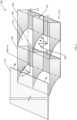
- Light source 202illuminates light guide 204, but it is placed in a cavity 208 of adjacent light guide 206.
- Light guide 206is meanwhile illuminated by light source 203.
- Cavity 208is an arbitrarily shaped void, hollow, opening, or the like sufficiently large to hold, completely or partially, light source 202.
- a cavityis form fitting to partially encapsulate a light source (e.g., cavity closely follows, at least in part, the contours of the light source).
- surface 210 of light guide 206defines size and shape of cavity 208. Further details relating to surface 210 are described more fully below in connection with Figs. 3A-3E .
- light source 202is physically mounted to light guide 204. This can be accomplished by a form factor housing both light source 202 and light guide 204. Light source 202 is can behoused with adjacent light guide 206. These structures containing one light guide and a one or more light sources (e.g., one white LED, three LED sources for red green blue, or the like), referred hereinafter as a "tile assembly,” provide benefits beyond compactness, such as a modular design.
- a one or more light sourcese.g., one white LED, three LED sources for red green blue, or the like
- Light guidescan be glass, polymer, semiconductor, plastic, or the like whether as slab, planar, rib, strip, segmented, or fiber structure.
- Light guides 204, 206direct electromagnetic waves in the optical spectrum (e.g., light with a wavelength between about 380 to 800 nanometers) or a subset of the optical spectrum.
- Light guide 204guides at least the desired wavelength(s) associated with light source 202.
- light guide 204is configured to reflect light in an outwards direction through a display's optical stack and ultimately to a viewer.
- a surface of a light guidesuch as surface 210 of light guide 206, is reflective.
- a reflective layercan be deposited (including by chemical vapor deposition), applied or affixed to, or under, to light guide 206 at surface 210.
- the reflective layerprovides a specular reflection surface or diffuse reflection surface, depending on desirability.
- Example materials for the reflective layerinclude one or more of: metals (e.g., aluminum, gold, silver, copper, brass, mercury, nickel or the like), polished metals, paint (e.g., white paint, glossy paint, matte paint), optically reflective silicone, water, and plastic.
- the reflected light from light guide 206can be further processed by subsequent elements in the optical stack.
- an optional layer 212, overlaid on one or more light guides,can diffuse the light for improved uniformity or alter the point spread function for less or more contribution to adjacent pixels.
- Light source 202can be a light-emitting diode (LED), organic light-emitting diode (OLED), active matrix organic LED, light-emitting electrochemical cell, field-induced electroluminescent polymer, cold cathode lamp, cold cathode fluorescent lamp, laser, phosphor coated LED, quantum dot coated LED, incandescent bulb, or any suitable source of electromagnetic waves of an appropriate wavelength, preferably thinner than the light guides.
- a combination of light sources of differing technologiescan be employed in panel 200.
- light sources 202 and 203can both be LEDs, but they need not be the same (e.g., as a specific embodiment, light source 202 can be an OLED, and light source 203 can be quantum dot coated LED).
- light sources 202, 203produce a broad spectrum light (e.g., white light) to illuminate light guides 204, 206.
- Colorcan be imparted to the light exiting light guides 204, 206 by several techniques.
- subsequent color filters in the optical pathcan be used to produce each of the primary colors, such as red, green and blue.
- a liquid crystal panel(not shown in Fig. 2 ) with subpixel color filters can be used.
- a matrix array of quantum dot subpixel areas in the optical stack above a light guidecan also convert light respectively to individual primary colors, e.g., red, blue, green and/or yellow.
- surface 210can optionally be a layer of quantum dots (i.e., semiconductor nanocrystals, when under excitation, emit light dependent on its size and shape) to generate broad spectrum light later imparted with color by filtering.
- the layer of quantum dotscan be within, above, or below surface 210.
- the light guidescan reflect blue or ultraviolet light to the subsequent optical stack, which can include a quantum dot layer of a matrix of red light generating, green light generating, and blue light generating areas of quantum dots. If the appropriate blue light is directly generated by light sources 202, 203, then the blue light generating area can be replaced with either a transparent filter or no filter at all (e.g., a cut-out to pass light, without alteration).
- light sourcese.g., light source 202 are positioned wholly within a cavity 208 formed by an adjacent light guide (e.g., light guide 206).
- Light source 202is completely within cavity 208.
- a light sourceshould not extend below the lowest (bottom) side 214, relative to an optical stack of a display device, of either its corresponding light guide or its adjacent light guide.
- the light sourceshould not extend above the highest (top) side 216 of either its corresponding light guide or its adjacent light guide
- thickness of the tile assemblyis enlarged.
- Figs. 3A, 3B, 3C, 3D, and 3Eillustrate simplified cross-sectional views of exemplary HDR panels, according to embodiments of the present invention.
- Fig. 3Ashows a linear surface 304.
- the slant angle of linear surface 304can range from about 1° to about 89°, preferably about 10° to about 70°, and more preferably about 30° to about 60°. In another embodiment, surface 304 can vary non-linearly.
- the desired point spread function (PSF, a measure of the degree of spreading of a point object) of the reflected light, as well as sizing of cavity 306,will influence acceptable slant angles.
- PSFpoint spread function
- cavity 306is sufficiently ample to house light source 308, whether light source 308 is integrated as a tile assembly with light guide 310 or as a standalone light source device. Such an arrangement reduces thickness 302, compared to stacking an entire thickness of a light guide plus height of a light source.
- light guidesinclude multi-faceted, convex or concave, reflection surfaces 325 and 326, although reflection surfaces can be smoothed to avoid sharp angles.
- the angle and number of facetsinfluence the PSF of the reflected light. In some instances, PSF that spread beyond one pixel area it is preferable. This increased PSF size reduces blocking artifacts associated with abrupt illumination changes at pixel boundaries.
- Fig. 3Dshows an undulating surface 327, which can be any waveform, such as sinusoidal, square, triangle, sawtooth or the like, or combinations of the foregoing.
- the waveformcan be either uniform or non-uniform in frequency or amplitude. For example, about a proximal start of surface 327 can have a higher frequency than about the distal end of surface 327.
- surfaces 325, 326, and 327can vary with height, depth, and/or length (in all three dimensions). In other words, one side of a reflective surface (e.g., left side) can differ from its opposite side (e.g., right side) or its center. In an example, a reflecting surface in three dimensions can vary with azimuth, elevation, or both.
- the proximal start 328, 329 of reflection surfaces 325 and 326is disposed away by a length 330 from illuminating light sources.
- Length 330can substantially range from about 0% to about 99% of the length of the entire light guide, but preferably 35% to 85%.
- the distal end of reflection surfaces 325 and 326need not abut the end of the light guide, nor coincide with a top surface (e.g., 331) of the light guide - in other words, surfaces 325, 326 can be less than thickness 302.
- a single light sourcee.g., white, blue or UV LED
- primary light sourcesare arranged as a group 330.
- Group 330is collectively housed, partially or wholly, in cavity 306. In other words, the primary light sources share a single light guide per group.
- Fig. 3Eillustrates a simplified cross-sectional view of exemplary HDR panels, according to another embodiment of the present invention.
- a group 330 of primary light sourcesilluminates two opposite facing light guides 350 and 352. Fewer light sources are needed, thus saving on bill of materials (BoM) cost, but reducing resolution for local dimming control.
- This implementationcan earn further BoM savings by using group 330 to illuminate four or more light guides organized radially about group 330.
- an "expanded tile assembly," as a single module,can include group 330 and its plurality of illuminated light guides.
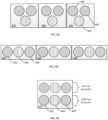
- Figs. 4A, 4B and 4Cillustrates exemplary groups 400, 450, 475 of primary light sources, according to an embodiment of the present invention.
- Groups 400, 450 and 475can be applied to the embodiments described above in connection with Figs. 2 and 3A-3D .
- Groups 400 and 450are illustrated to show three primary light sources 402, 404, and 406; however, there can be two, four, 5 or more primaries in an HDR panel.
- an HDR panelcan implement any one of RGB, RGB + yellow, RGB + white, or RGB + yellow + cyan.
- group 475For a three dimensional (3D) rendering panel utilizing spectral separation, group 475 includes six primary light sources. A viewer wears spectrally sensitive glasses such that different components of the illuminated light are directed to the viewers' left and right eyes. As an example, a first red primary is perceived in a viewer's left eye, but a second red primary (spectrally different from the first) is filtered by the left eye lenses of the 3D glasses. For the right eye, the second red primary is perceptible, but not the first. Accordingly, group 475 includes two sets of primaries that do not overlap spectrally. Additional details about 3D spectral separation as used for cinema projection are described in US Patent No. 7,784,938 .
- Fig. 5illustrates a tile assembly 500 for subpixel resolution, according to an example not part of the claimed invention.
- a plurality of light sourcese.g., 502, 504, and 506 or more
- emanating a display's primary colorsare coupled to respective light guides (e.g., 508, 510, and 512).
- light source 502can be a red LED
- light source 504can be a green LED
- light source 506can be a blue LED.
- the light output from light guides 508, 510, and 512provide subpixel color modulation by the backlight, as well as further modulation by a liquid crystal display (not shown).
- This tile assemblyavoids the use of color filters in the optical stack and quantum dots. It should be appreciated that the resulting spatial resolution of the HDR panel comprising an array of tile assemblies 500 can be less than, equal to, or greater than other optical components, such as the liquid crystal panel.
- Figs. 6A-6Dillustrate an exemplary HDR display.
- the structures depicted in Figs. 6A-6Dcan be applied to one or more of the embodiments described above for Figs. 2 , 3A-3D , 4A-4C , and 5 , as would be readily apparent by a person skilled in the art benefiting from the teachings of this specification. It will also be apparent that one or more of the depicted layers in Figs. 6A-6D are optional. For example, if the tile assembly 602 includes quantum dots, then quantum dot layer 606 can be omitted.
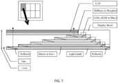
- Fig. 7illustrates an exemplary HDR display with a compact design, according to an embodiment not part of the claimed invention.
- Light sources(such as white LEDs, RGB LED groups, etc.) are mounted along the edges of an LCD display.
- the light sourcesare tiled as closely as possible in two dimensions along the edge of the display, essentially creating a low-resolution backlight.
- the lightis directed to the desired location behind the LCD display.
- the light sourcesemit light into a planar light guide.
- the lightis transmitted along the light guide either by total internal reflection (TIR) or by reflective boundaries.
- TIRtotal internal reflection
- the light sourcestransmit light at 90 degrees to the light guide to allow for the light guides to be very thin (order of um).
- the lightis reflected along the light guides using an angled reflector or TIR.
- the LEDscould emit light directly into the light guide.
- the backlight opticscan be tiled or continuous across the display, with light being emitted along both top and bottom, or left and right edges. Instead of reflecting the light upwards towards the LCD as described above for Fig. 7 , a top surface of the light guide could be diffused if using TIR, or the reflector could be terminated to eject light from the light guide in the desired location.
Landscapes
- Physics & Mathematics (AREA)
- General Physics & Mathematics (AREA)
- Optics & Photonics (AREA)
- Planar Illumination Modules (AREA)
- Liquid Crystal (AREA)
Description
- This application is a European divisional application of Euro-PCT patent application
EP 1574963.5 (reference: D09027EP01), filed 03 August 2015 . - This application claims the benefit of priority to
United States Provisional Patent Application No. 62/032,832 filed 4 August 2014 - The present invention relates generally to display techniques for high dynamic range images, and in particular, to compact displays for local dimming.
- Dynamic range is the ratio of intensity of the highest luminance parts of an image scene and the lowest luminance parts of a scene. For example, the image projected by a video projection system may have a maximum dynamic range of 300:1.
- The human visual system is capable of recognizing features in scenes which have very high dynamic ranges. For example, a person can look into the shadows of an unlit garage on a brightly sunlit day and see details of objects in the shadows even though the luminance in adjacent sunlit areas may be thousands of times greater than the luminance in the shadow parts of the scene. To create a realistic rendering of such a scene can require a display having a dynamic range in excess of 1000:1. The term "high dynamic range" (HDR) means dynamic ranges of at least 800:1.
- Conventional display technology, using direct-lit local dimming (as an example, described by
US Patent No. 8,277,056 , "Locally Dimmed Display,"), is capable of rendering images in a manner that faithfully reproduces high dynamic ranges. This is accomplished by independent modulation of light sources, as well as modulation by one or more liquid crystal panels, for improved contrast. However, a direct-lit panel 100 cannot do so in a form factor sufficiently thin for many applications (e.g., a cellular telephone display). As shown inFig. 1A , the width 102 of a direct-lit panel stacks the light sources, liquid crystal panel, and intervening optics (such as, a diffusion layer). - As an alternative to direct-lit panels, edge-lit technology (as an example, described in
US Patent No. 8,446,351 , "Edge Lit LED based Locally Dimmed Display," ) is employed with mixed results. As shown inFig. 1B , an edge-lit panel 150 is thinner by not stacking a light source, andwidth 152 driven by the liquid crystal panel, light guide, and any intervening optics (not shown). That said, edge-lit panel 150 suffers from noticeably reduced HDR performance because light source modulation is row dependent and light intensity decreases along the length of the light guide (e.g., non-uniformity as a function of distance from the light source). - Accordingly, a need exists for a compact (e.g., thin) local dimming display capable of reproducing a wide range of light intensities.
US 2011/090423 A1 describes an illumination device having a partially transmissive front reflector, a back reflector, and a cavity between them. At least one light injector including a baffle and a light source is disposed in the cavity. The light injector is capable of injecting partially collimated light into the cavity. The output area of the illumination device can be increased by disposing light injectors progressively within the cavity, without sacrificing uniformity of the light emitted through the output area.EP 2 336 630 A1 describes an illumination device with first and second reflecting sheets. Each of the first reflecting sheets is provided so as to cover the opposite surface of a corresponding lightguide which is opposite to a light exit surface of the corresponding lightguide. Each of the second reflecting sheets is provided on the opposite surface of a corresponding first reflecting sheet which is opposite to a surface thereof facing a corresponding lightguide, over a corresponding first gap, wherein each of the first gaps is defined between adjacent two of the lightguides that do not to overlap each other. Each of the second reflecting sheets covers a region where no first reflecting sheet is provided in the corresponding first gap and extends over the adjacent two of the lightguides.US 2006/0221638 A1 describes a light-emitting apparatus including a plurality of adjacent, overlapping light-guide plates formed of substantially transparent material and a plurality of light sources. Each of the light-guide plates has first and second ends, one or more substantially transparent surfaces through which light is emitted, and one or more reflective surfaces to redirect light within the light-guide plate. Where first and second light-guide plates are adjacent, the first end of the first light-guide plate underhangs the second end of the second light-guide plate, and is positioned opposite a primary light-emitting side of the apparatus. The plurality of light sources are optically coupled to the first ends of the light-guide plates so as to illuminate the interiors of the light-guide plates.EP 2 378 325 A2 describes a plurality of aligned backlight blocks. Each block includes light sources and a unit light guide plate for guiding light from the light sources to the side of a liquid crystal panel. Unit diffusion patterns are formed in a zigzag alignment on the unit light guide plate and another diffusion pattern is formed on the back of the unit light guide plate. One side of the unit light guide plate is defined as a light entrance surface. LEDs as the light sources are aligned along the light entrance surface.US 2010/149788 A1 describes a display apparatus including a display panel, a light source and a plurality of a light guiding plate. The light guiding plate includes light incident, counter, light emitting and rear surfaces. The counter and rear surfaces are respectively opposite to the light incident and light emitting surfaces. The light emitting surface includes an ineffective light emitting area making contact with the light incident surface and an effective light emitting area connecting the ineffective light emitting area with the counter surface. The counter surface of a first light guiding plate is disposed overlapping the light incident surface of a second light guiding plate along a first direction, so that the rear surface partially overlaps with the effective light emitting area of the second light guiding plate, and the light guiding plates collectively form a light guiding plate array along the first direction.US 2008/084706 A1 describes a display comprising a light source and an image display panel disposed in an optical path from the light source. The light source comprises a primary light source for illuminating a re-emission material which comprises at least a first nanophosphor material for, when illuminated by light from the primary light source, re-emitting light in a first wavelength range different from the emission wavelength range of the primary light source. The image display panel comprises a first filter having a first narrow passband or a first narrow absorption band, the first narrow passband or first narrow absorption band being aligned or substantially aligned with the first wavelength range. The combination of a narrow wavelength range emitted by the first nanophosphor material and the narrow passband or narrow absorption band of the filter allows a display with high efficiency and a high NTSC ratio to be obtained.- The approaches described in this section are approaches that could be pursued, but not necessarily approaches that have been previously conceived or pursued. Therefore, unless otherwise indicated, it should not be assumed that any of the approaches described in this section qualify as prior art merely by virtue of their inclusion in this section. Similarly, issues identified with respect to one or more approaches should not assume to have been recognized in any prior art on the basis of this section, unless otherwise indicated.
- The invention is defined by the independent claims. Embodiments of the invention are defined in the dependent claims. Techniques are provided for a high dynamic range panel that includes an array of light sources illuminating a corresponding array of light guides. A light source of the array illuminates a first light guide. The light source directly underlies, such as in a cavity, a second light guide that is adjacent to the first light guide. The light source does not extend below a bottom side of either the first light guide or the second light guide to reduce thickness of the panel.
- In an example, not part of the claimed invention, an apparatus includes a first light source to illuminate a first light guide with blue or ultraviolet light. The first light source is within a cavity formed by at least the first light guide and a second light guide. A second light source illuminates the second light guide with the blue or ultraviolet light. The second light guide is adjacent to the first light guide. The first light guide includes a sloped surface generating a broad spectrum light (e.g., white light) from the blue or ultraviolet light. The first light source does not extend beyond the cavity.
- As another example of the present disclosure, not part of the claimed invention, an apparatus includes an array of light sources respectively illuminating an array of light guides. A first light source of the array of light sources directly underlies a first light guide illuminated by a second light source in the array. The first light source does not extend below a bottom side of the first light guide. The first light guide includes a multi-faceted reflective layer that directs light to a different direction.
- In an aspect of the present invention, an apparatus for a display includes a first group of primary light sources to illuminate in a first direction a first light guide with a first light. The first light guide directs the first light to a second direction perpendicular to the first direction. The first group of primary light sources are disposed within a cavity of a second light guide. Both the second light guide and the cavity are coupled to the first light guide in the first direction in a tile assembly without overlapping the first light guide. A second group of primary light sources illuminates in the first direction the second light guide with a second light. The second light guide has a sloped surface to direct the second light to the second direction. The cavity underlies the sloped surface in a direction opposite to the second direction. The second light guide is adjacent to the first light guide. The first group of primary light sources underlies in the second direction the second light guide. The first and second light guides each may include a multi-faceted reflective layer to direct light to the second direction. The first group of primary light sources does not extend below a bottom side of the second light guide.
- The present invention is illustrated by way of example, and not by way of limitation, in the figures of the accompanying drawings and in which like reference numerals refer to similar elements and in which:
Figs. 1A and 1B illustrate conventional direct lit and edge-lit displays, respectively.Fig. 2 illustrates an exemplary HDR array panel, according to an embodiment of the present invention;Figs. 3A-3E illustrate simplified cross-sectional views of exemplary HDR color array panels, according to embodiments of the present invention;Figs. 4A-4C illustrates exemplary groups of primary light sources, according to an embodiment of the present invention;Fig. 5 illustrates a tile assembly for subpixel resolution, according to an embodimentnot part of the claimed invention; andFigs. 6A-6D illustrate an exemplary HDR display;Fig. 7 illustrates an exemplary HDR display with a compact design, according to an embodiment not part of the claimed invention.- Example possible embodiments, which relate to HDR displays used for televisions, computer displays, tablets, PDAs, mobile cellular telephones, advertising displays or the like, are described herein. In the following description, for the purposes of explanation, numerous specific details are set forth in order to provide a thorough understanding of the present invention. It will be apparent, however, that the present invention may be practiced without these specific details. In other instances, well-known structures and devices are not described in exhaustive detail, in order to avoid unnecessarily occluding, obscuring, or obfuscating the present invention.
Fig. 2 illustrates anexemplary HDR panel 200.HDR panel 200 is a two dimensional array of pixel elements (e.g., 960 x 640; 1136 x 640; 1920 x 1080; 4096 x 2160; 3840 x 2160), each pixel element includes at least a light source optically coupled to a light guide (i.e., an optical waveguide, such as optical fiber) in this example. Each light source is independently controllable for fine local dimming, or a subset of these light sources can be controlled in concert for coarse local dimming. Further, the spatial resolution ofHDR panel 200 need not be the same, 1:1, as other optical elements, such as a liquid crystal panel (not shown). For example, the spatial resolution ofHDR panel 200 can be 1:2, 1:4, 1:8 or less of the liquid crystal panel. In other words, a single light source of the backlight can be used to reproduce multiple pixels in an area of a display.- For improved compactness of
panel 200, light sources are disposed within cavities underlying adjacent light guides.Light source 202 illuminateslight guide 204, but it is placed in acavity 208 of adjacentlight guide 206.Light guide 206 is meanwhile illuminated bylight source 203.Cavity 208 is an arbitrarily shaped void, hollow, opening, or the like sufficiently large to hold, completely or partially,light source 202. In a specific embodiment, a cavity is form fitting to partially encapsulate a light source (e.g., cavity closely follows, at least in part, the contours of the light source). For simplicity,surface 210 oflight guide 206 defines size and shape ofcavity 208. Further details relating to surface 210 are described more fully below in connection withFigs. 3A-3E . - In one example,
light source 202 is physically mounted tolight guide 204. This can be accomplished by a form factor housing bothlight source 202 andlight guide 204.Light source 202 is can behoused with adjacentlight guide 206. These structures containing one light guide and a one or more light sources (e.g., one white LED, three LED sources for red green blue, or the like), referred hereinafter as a "tile assembly," provide benefits beyond compactness, such as a modular design. - Light guides (e.g., 204, 206) can be glass, polymer, semiconductor, plastic, or the like whether as slab, planar, rib, strip, segmented, or fiber structure. Light guides 204, 206 direct electromagnetic waves in the optical spectrum (e.g., light with a wavelength between about 380 to 800 nanometers) or a subset of the optical spectrum.
Light guide 204 guides at least the desired wavelength(s) associated withlight source 202. - Since
light source 202 provides lateral illumination oflight guide 204,light guide 204 is configured to reflect light in an outwards direction through a display's optical stack and ultimately to a viewer. In an implementation of the present invention, a surface of a light guide, such assurface 210 oflight guide 206, is reflective. A reflective layer can be deposited (including by chemical vapor deposition), applied or affixed to, or under, tolight guide 206 atsurface 210. The reflective layer provides a specular reflection surface or diffuse reflection surface, depending on desirability. Example materials for the reflective layer include one or more of: metals (e.g., aluminum, gold, silver, copper, brass, mercury, nickel or the like), polished metals, paint (e.g., white paint, glossy paint, matte paint), optically reflective silicone, water, and plastic. The reflected light fromlight guide 206 can be further processed by subsequent elements in the optical stack. InFig. 2 , anoptional layer 212, overlaid on one or more light guides, can diffuse the light for improved uniformity or alter the point spread function for less or more contribution to adjacent pixels. Light source 202 can be a light-emitting diode (LED), organic light-emitting diode (OLED), active matrix organic LED, light-emitting electrochemical cell, field-induced electroluminescent polymer, cold cathode lamp, cold cathode fluorescent lamp, laser, phosphor coated LED, quantum dot coated LED, incandescent bulb, or any suitable source of electromagnetic waves of an appropriate wavelength, preferably thinner than the light guides. A combination of light sources of differing technologies can be employed inpanel 200. In other words,light sources light source 202 can be an OLED, andlight source 203 can be quantum dot coated LED).- In an example of the present invention,
light sources light guides Fig. 2 ) with subpixel color filters can be used. - A matrix array of quantum dot subpixel areas in the optical stack above a light guide can also convert light respectively to individual primary colors, e.g., red, blue, green and/or yellow. When
light sources surface 210 can optionally be a layer of quantum dots (i.e., semiconductor nanocrystals, when under excitation, emit light dependent on its size and shape) to generate broad spectrum light later imparted with color by filtering. Alternatively, the layer of quantum dots can be within, above, or belowsurface 210. As another example, the light guides can reflect blue or ultraviolet light to the subsequent optical stack, which can include a quantum dot layer of a matrix of red light generating, green light generating, and blue light generating areas of quantum dots. If the appropriate blue light is directly generated bylight sources - As described above, light sources (e.g., light source 202) are positioned wholly within a
cavity 208 formed by an adjacent light guide (e.g., light guide 206).Light source 202 is completely withincavity 208. For a thinner tile assembly, a light source should not extend below the lowest (bottom)side 214, relative to an optical stack of a display device, of either its corresponding light guide or its adjacent light guide. Similarly, the light source should not extend above the highest (top)side 216 of either its corresponding light guide or its adjacent light guide To the extent the light source extends above or below the light guides, thickness of the tile assembly is enlarged. Figs. 3A, 3B, 3C, 3D, and 3E illustrate simplified cross-sectional views of exemplary HDR panels, according to embodiments of the present invention.Fig. 3A shows alinear surface 304. The slant angle oflinear surface 304 can range from about 1° to about 89°, preferably about 10° to about 70°, and more preferably about 30° to about 60°. In another embodiment,surface 304 can vary non-linearly. The desired point spread function (PSF, a measure of the degree of spreading of a point object) of the reflected light, as well as sizing ofcavity 306, will influence acceptable slant angles. In an example,cavity 306 is sufficiently ample tohouse light source 308, whetherlight source 308 is integrated as a tile assembly withlight guide 310 or as a standalone light source device. Such an arrangement reducesthickness 302, compared to stacking an entire thickness of a light guide plus height of a light source.- Referring to
Figs. 3B and 3C , light guides include multi-faceted, convex or concave, reflection surfaces 325 and 326, although reflection surfaces can be smoothed to avoid sharp angles. The angle and number of facets (e.g., two, three, four, five, six, seven or more facets) influence the PSF of the reflected light. In some instances, PSF that spread beyond one pixel area it is preferable. This increased PSF size reduces blocking artifacts associated with abrupt illumination changes at pixel boundaries.Fig. 3D shows an undulatingsurface 327, which can be any waveform, such as sinusoidal, square, triangle, sawtooth or the like, or combinations of the foregoing. The waveform can be either uniform or non-uniform in frequency or amplitude. For example, about a proximal start ofsurface 327 can have a higher frequency than about the distal end ofsurface 327. It should be appreciated, based on the teachings herein, that surfaces 325, 326, and 327 can vary with height, depth, and/or length (in all three dimensions). In other words, one side of a reflective surface (e.g., left side) can differ from its opposite side (e.g., right side) or its center. In an example, a reflecting surface in three dimensions can vary with azimuth, elevation, or both. - As depicted in the figures, the
proximal start length 330 from illuminating light sources.Length 330 can substantially range from about 0% to about 99% of the length of the entire light guide, but preferably 35% to 85%. Likewise, the distal end of reflection surfaces 325 and 326 need not abut the end of the light guide, nor coincide with a top surface (e.g., 331) of the light guide - in other words, surfaces 325, 326 can be less thanthickness 302. These considerations can also apply toreflective surface 304 ofFig. 3A . - In
Figs. 3B and 3C , instead of a single light source (e.g., white, blue or UV LED) for each light guide, primary light sources are arranged as agroup 330.Group 330 is collectively housed, partially or wholly, incavity 306. In other words, the primary light sources share a single light guide per group. Fig. 3E illustrates a simplified cross-sectional view of exemplary HDR panels, according to another embodiment of the present invention. In this example, agroup 330 of primary light sources illuminates two opposite facing light guides 350 and 352. Fewer light sources are needed, thus saving on bill of materials (BoM) cost, but reducing resolution for local dimming control. This implementation can earn further BoM savings by usinggroup 330 to illuminate four or more light guides organized radially aboutgroup 330. In this scenario, an "expanded tile assembly," as a single module, can includegroup 330 and its plurality of illuminated light guides.Figs. 4A, 4B and 4C illustratesexemplary groups Groups Figs. 2 and3A-3D .Groups light sources - For a three dimensional (3D) rendering panel utilizing spectral separation,
group 475 includes six primary light sources. A viewer wears spectrally sensitive glasses such that different components of the illuminated light are directed to the viewers' left and right eyes. As an example, a first red primary is perceived in a viewer's left eye, but a second red primary (spectrally different from the first) is filtered by the left eye lenses of the 3D glasses. For the right eye, the second red primary is perceptible, but not the first. Accordingly,group 475 includes two sets of primaries that do not overlap spectrally. Additional details about 3D spectral separation as used for cinema projection are described inUS Patent No. 7,784,938 . Fig. 5 illustrates atile assembly 500 for subpixel resolution, according to an example not part of the claimed invention. A plurality of light sources (e.g., 502, 504, and 506 or more) emanating a display's primary colors are coupled to respective light guides (e.g., 508, 510, and 512). For example,light source 502 can be a red LED,light source 504 can be a green LED, andlight source 506 can be a blue LED. The light output fromlight guides tile assemblies 500 can be less than, equal to, or greater than other optical components, such as the liquid crystal panel.Figs. 6A-6D illustrate an exemplary HDR display. The structures depicted inFigs. 6A-6D can be applied to one or more of the embodiments described above forFigs. 2 ,3A-3D ,4A-4C , and5 , as would be readily apparent by a person skilled in the art benefiting from the teachings of this specification. It will also be apparent that one or more of the depicted layers inFigs. 6A-6D are optional. For example, if thetile assembly 602 includes quantum dots, thenquantum dot layer 606 can be omitted.Fig. 7 illustrates an exemplary HDR display with a compact design, according to an embodiment not part of the claimed invention.- Light sources (such as white LEDs, RGB LED groups, etc.) are mounted along the edges of an LCD display. The light sources are tiled as closely as possible in two dimensions along the edge of the display, essentially creating a low-resolution backlight.
- The light is directed to the desired location behind the LCD display. First, the light sources emit light into a planar light guide. The light is transmitted along the light guide either by total internal reflection (TIR) or by reflective boundaries. Eventually, light is reflected upwards through a diffuser and LCD. As illustrated in
Fig. 7 , the light sources transmit light at 90 degrees to the light guide to allow for the light guides to be very thin (order of um). The light is reflected along the light guides using an angled reflector or TIR. Alternatively, the LEDs could emit light directly into the light guide. - The backlight optics can be tiled or continuous across the display, with light being emitted along both top and bottom, or left and right edges. Instead of reflecting the light upwards towards the LCD as described above for
Fig. 7 , a top surface of the light guide could be diffused if using TIR, or the reflector could be terminated to eject light from the light guide in the desired location. - This specification often refers to colors, such as blue, ultraviolet, red, green, etc. Without limiting the generality of the teachings herein, light colors can be within about the following ranges for one or moreexamples of the present disclosure:
- (i) blue - 450 to 490 nanometers (nm);
- (ii) red - 635 to 700 nm;
- (iii) green - 490 to 560 nm;
- (iv) ultraviolet - 10 nm to 400 nm (with near UV, 300 to 400 nm);
- (v) white - a combination of visible light of different wavelengths perceived by the human visual system as having no specific color (e.g., average noon sunlight; CIE (International Commission on Illumination) standard illuminant D65), visible light generally ranging from 380 nm to 800 nm.
- In the foregoing specification, possible embodiments of the invention have been described with reference to numerous specific details that may vary from implementation to implementation. Thus, the sole and exclusive indicator of what is the invention, and is intended by the applicants to be the invention, is the appended set of claims.
- The specification and drawings are, accordingly, to be regarded in an illustrative rather than a restrictive sense.
- The following references, in addition to any reference cited above, are noted:
- (i) International Publication No.
WO 2006/064500 , Device and method for optical resizing; - (ii)
US Patent Publication No. 2007/0086712 Device and method for optical resizing and backlighting; - (iii)
US Patent Publication No. 2008/0205078 Illumination tiles and related methods; - (iv)
US Patent Publication No. 2008/0205080 Tiled illumination assembly and related methods; - (v)
US Patent No. 7,311,431 , Light-emitting apparatus having a plurality of adj acent, overlapping light-guide plates; - (vi)
US Patent No. 6,768,525 , Color isolated backlight for an LCD; and - (vii)
European Patent Application Publication No. 509096
Claims (13)
- An apparatus (200) for a display, the apparatus (200) comprising:
a first group of primary light sources (202; 400; 450; 475) to illuminate in a first direction a first light guide (204) with a first light, the first light guide (204) directing the first light to a second direction perpendicular to the first direction, the first group of primary light sources (202; 400; 450; 475) disposed within a cavity (208) of a second light guide (206), both the second light guide (206) and the cavity (208) coupled to the first light guide (204) in the first direction in a tile assembly without overlapping the first light guide (204);
a second group of primary light sources (203; 400; 450; 475) to illuminate in the first direction the second light guide (206) with a second light, the second light guide (206) having a sloped surface configured to direct the second light to the second direction, the cavity (208) underlying the sloped surface (210) in a direction opposite to the second direction. - The apparatus (200) of claim 1 wherein the first (202; 400; 450; 475) and second (203; 400; 450; 475) group of light sources comprise at least one of blue and ultraviolet light emitting diodes.
- The apparatus (200) of claim 2 wherein the sloped surface (210) comprises a quantum dot layer.
- The apparatus (200) of claim 3 wherein the quantum dot layer produces a red light from the at least one of blue and ultraviolet light.
- The apparatus (200) of claim 3 wherein the quantum dot layer produces a green light from the at least one of blue and ultraviolet light.
- The apparatus (200) of any of claims 1-5 wherein the sloped surface comprises a multi-faceted reflective layer (325, 326, 327).
- The apparatus (200) of claim 6 wherein the multi-faceted reflective layer (325, 326, 327) includes at least 3 facets.
- The apparatus (200) of any of claims 1-7 wherein the first group of primary light sources (202; 400; 450; 475) and the second light guide (206) are physically coupled as a tile assembly.
- The apparatus (200) of any of claims 1-8 wherein the first group of primary light sources (202; 400; 450; 475) and the first light guide (204) are physically coupled as a tile assembly.
- The apparatus of any of the previous claims, wherein the first group of primary light sources and/or the second group of primary light sources comprise two, three, four, five or more than five primaries.
- The apparatus of claim 10, wherein the primaries comprise red, green and blue (RGB), or RGB and white, or RGB and yellow and cyan.
- The apparatus according to any one of the previous claims, wherein the first group of primary light sources and/or the second group of primary light sources comprises three sub-groups (400; 450) of primary light sources.
- The apparatus according to any one of the claims 1 to 11, wherein the first group (475) of primary light sources and/or the second group (475) of primary light sources comprise two subsets of three corresponding primaries, wherein the display is a three dimensional (3D) rendering display using spectral separation between each corresponding primary in the two subsets.
Applications Claiming Priority (3)
| Application Number | Priority Date | Filing Date | Title |
|---|---|---|---|
| US201462032832P | 2014-08-04 | 2014-08-04 | |
| EP15747963.5AEP3177868B1 (en) | 2014-08-04 | 2015-08-03 | Tiled assemblies for a high dynamic range display panel |
| PCT/US2015/043428WO2016022476A1 (en) | 2014-08-04 | 2015-08-03 | Tiled assemblies for a high dynamic range display panel |
Related Parent Applications (1)
| Application Number | Title | Priority Date | Filing Date |
|---|---|---|---|
| EP15747963.5ADivisionEP3177868B1 (en) | 2014-08-04 | 2015-08-03 | Tiled assemblies for a high dynamic range display panel |
Publications (2)
| Publication Number | Publication Date |
|---|---|
| EP3889498A1 EP3889498A1 (en) | 2021-10-06 |
| EP3889498B1true EP3889498B1 (en) | 2024-10-16 |
Family
ID=53785801
Family Applications (2)
| Application Number | Title | Priority Date | Filing Date |
|---|---|---|---|
| EP21170091.9AActiveEP3889498B1 (en) | 2014-08-04 | 2015-08-03 | Tiled assemblies for a high dynamic range display panel |
| EP15747963.5AActiveEP3177868B1 (en) | 2014-08-04 | 2015-08-03 | Tiled assemblies for a high dynamic range display panel |
Family Applications After (1)
| Application Number | Title | Priority Date | Filing Date |
|---|---|---|---|
| EP15747963.5AActiveEP3177868B1 (en) | 2014-08-04 | 2015-08-03 | Tiled assemblies for a high dynamic range display panel |
Country Status (5)
| Country | Link |
|---|---|
| US (1) | US10371884B2 (en) |
| EP (2) | EP3889498B1 (en) |
| JP (1) | JP6389321B2 (en) |
| CN (1) | CN106662703B (en) |
| WO (1) | WO2016022476A1 (en) |
Families Citing this family (7)
| Publication number | Priority date | Publication date | Assignee | Title |
|---|---|---|---|---|
| US10656465B2 (en) | 2015-05-29 | 2020-05-19 | Harman International Industries, Incorporated | Wide color-gamut vehicle infotainment display system with quantum dot element |
| EP3304186B1 (en) | 2015-05-29 | 2023-01-04 | Harman International Industries, Incorporated | Wide color-gamut vehicle infotainment display system |
| US11112653B2 (en)* | 2015-05-29 | 2021-09-07 | Harman International Industries, Incorporated | Wide color-gamut vehicle infotainment display system with quantum dot element |
| KR102507626B1 (en)* | 2017-10-31 | 2023-03-07 | 엘지디스플레이 주식회사 | Volumetric type 3-dimension display device |
| WO2019134822A1 (en)* | 2018-01-02 | 2019-07-11 | Signify Holding B.V. | Luminaire comprising a surface tile and a lighting device |
| CN108535911A (en)* | 2018-05-21 | 2018-09-14 | 京东方科技集团股份有限公司 | A kind of transparent liquid crystal display device |
| TWI709259B (en)* | 2019-07-10 | 2020-11-01 | 群光電能科技股份有限公司 | Light emitting device |
Family Cites Families (30)
| Publication number | Priority date | Publication date | Assignee | Title |
|---|---|---|---|---|
| EP0509096A4 (en) | 1990-11-02 | 1993-01-27 | Toray Industries, Inc. | Image display device and method of producing the same |
| US7046905B1 (en)* | 1999-10-08 | 2006-05-16 | 3M Innovative Properties Company | Blacklight with structured surfaces |
| US6768525B2 (en) | 2000-12-01 | 2004-07-27 | Lumileds Lighting U.S. Llc | Color isolated backlight for an LCD |
| EP1390806B1 (en) | 2001-02-27 | 2010-08-25 | Dolby Laboratories Licensing Corporation | High dynamic range display devices |
| JP4348457B2 (en) | 2002-03-13 | 2009-10-21 | ドルビー ラボラトリーズ ライセンシング コーポレイション | High dynamic range display, display controller, and image display method |
| CN1227562C (en) | 2002-12-30 | 2005-11-16 | 广辉电子股份有限公司 | Lightweight backlight module |
| JP4050726B2 (en)* | 2004-06-23 | 2008-02-20 | 株式会社東芝 | Decoding device |
| US7773849B2 (en) | 2004-12-14 | 2010-08-10 | Oms Displays Ltd. | Device and method for optical resizing and backlighting |
| CN101124497A (en) | 2004-12-14 | 2008-02-13 | Oms显示器有限公司 | Device and method for optical resizing |
| US7311431B2 (en)* | 2005-04-01 | 2007-12-25 | Avago Technologies Ecbu Ip Pte Ltd | Light-emitting apparatus having a plurality of adjacent, overlapping light-guide plates |
| KR100780205B1 (en)* | 2006-04-21 | 2007-11-27 | 삼성전기주식회사 | Backlight Unit for Liquid Crystal Display |
| TW200805912A (en)* | 2006-07-05 | 2008-01-16 | Apac Opto Electronics Inc | Transmission apparatus with fiber high-definition digital video data interface |
| EP1905955B1 (en)* | 2006-09-25 | 2009-04-22 | Siemens Aktiengesellschaft | Turbine rotor with locking plates and corresponding assembly method |
| GB2442505A (en)* | 2006-10-04 | 2008-04-09 | Sharp Kk | A display with a primary light source for illuminating a nanophosphor re-emission material |
| JP4735849B2 (en)* | 2006-10-26 | 2011-07-27 | ミネベア株式会社 | Surface lighting device |
| US20080205078A1 (en) | 2007-02-23 | 2008-08-28 | Luminus Devices, Inc. | Illumination tiles and related methods |
| US7784938B2 (en) | 2007-05-09 | 2010-08-31 | Dolby Laboratories Licensing Corporation | Method and system for shaped glasses and viewing 3D images |
| JP2010021131A (en)* | 2008-06-09 | 2010-01-28 | Hitachi Ltd | Display device and backlight unit used for the same |
| US20110090423A1 (en) | 2008-06-13 | 2011-04-21 | Wheatley John A | Illumination device with progressive injection |
| US20110164404A1 (en)* | 2008-09-30 | 2011-07-07 | Sharp Kabushiki Kaisha | Illumination device, surface light source device, and liquid crystal display apparatus |
| KR101539956B1 (en)* | 2008-12-16 | 2015-07-29 | 삼성디스플레이 주식회사 | Display device |
| KR20210022147A (en) | 2008-12-19 | 2021-03-02 | 가부시키가이샤 한도오따이 에네루기 켄큐쇼 | Method for driving display device |
| US8379172B2 (en)* | 2009-05-29 | 2013-02-19 | Panasonic Corporation | Liquid crystal display device |
| KR101565409B1 (en)* | 2009-06-02 | 2015-11-03 | 엘지전자 주식회사 | LED back-light unit |
| KR101611616B1 (en) | 2009-08-28 | 2016-04-11 | 엘지전자 주식회사 | Backlight unit and display apparatus thereof |
| WO2011030941A1 (en) | 2009-09-11 | 2011-03-17 | 단비기술 유한회사 | Local dimming backlight apparatus |
| EP2488915B1 (en)* | 2009-10-14 | 2014-12-24 | Dolby Laboratories Licensing Corporation | Variable flower display backlight system |
| JP5422473B2 (en)* | 2010-04-09 | 2014-02-19 | 日立コンシューマエレクトロニクス株式会社 | Video display device and backlight device used therefor |
| JP5754322B2 (en) | 2011-09-21 | 2015-07-29 | 日本電気硝子株式会社 | Capillary for encapsulating phosphor and wavelength conversion member |
| CN202511118U (en)* | 2011-11-25 | 2012-10-31 | 上海向隆电子科技有限公司 | Light-emitting module |
- 2015
- 2015-08-03EPEP21170091.9Apatent/EP3889498B1/enactiveActive
- 2015-08-03EPEP15747963.5Apatent/EP3177868B1/enactiveActive
- 2015-08-03USUS15/501,400patent/US10371884B2/enactiveActive
- 2015-08-03WOPCT/US2015/043428patent/WO2016022476A1/enactiveApplication Filing
- 2015-08-03JPJP2017506305Apatent/JP6389321B2/enactiveActive
- 2015-08-03CNCN201580039935.3Apatent/CN106662703B/enactiveActive
Also Published As
| Publication number | Publication date |
|---|---|
| US10371884B2 (en) | 2019-08-06 |
| US20170235041A1 (en) | 2017-08-17 |
| EP3177868B1 (en) | 2021-04-28 |
| CN106662703A (en) | 2017-05-10 |
| WO2016022476A1 (en) | 2016-02-11 |
| EP3177868A1 (en) | 2017-06-14 |
| CN106662703B (en) | 2020-08-18 |
| EP3889498A1 (en) | 2021-10-06 |
| JP6389321B2 (en) | 2018-09-12 |
| JP2017524229A (en) | 2017-08-24 |
Similar Documents
| Publication | Publication Date | Title |
|---|---|---|
| EP3889498B1 (en) | Tiled assemblies for a high dynamic range display panel | |
| CN114730044B (en) | Directional lighting and privacy displays | |
| EP2067065B1 (en) | Illumination system, luminaire and display device | |
| JP4838986B2 (en) | Luminance profile generator | |
| CA3130749C (en) | Dual view zone backlight, dual-mode display, and method employing directional emitters | |
| US7845826B2 (en) | Multilayered integrated backlight illumination assembly | |
| KR102033916B1 (en) | Crosstalk suppression in a directional backlight | |
| US8462292B2 (en) | Optically transmissive substrates and light emitting assemblies and methods of making same, and methods of displaying images using the optically transmissive substrates and light emitting assemblies | |
| US20110128471A1 (en) | Illumination panel and display | |
| CA3134524C (en) | Multi-zone backlight, multiview display, and method | |
| KR20090079929A (en) | Thin lighting device, display device and light emitting device | |
| US20150062963A1 (en) | Illumination system and method for backlighting | |
| JP2010170897A (en) | Edge light partial drive backlight unit, and liquid crystal display device | |
| US20180203300A1 (en) | Display device | |
| TWI851721B (en) | Light source, multiview backlight, and method with a bifurcated emission pattern | |
| US12326580B2 (en) | Multiview display and method using effective light sources | |
| WO2013161811A1 (en) | Surface light source device and liquid crystal display device | |
| KR20120106531A (en) | 3d image display apparatus and driving method thereof |
Legal Events
| Date | Code | Title | Description |
|---|---|---|---|
| PUAI | Public reference made under article 153(3) epc to a published international application that has entered the european phase | Free format text:ORIGINAL CODE: 0009012 | |
| STAA | Information on the status of an ep patent application or granted ep patent | Free format text:STATUS: THE APPLICATION HAS BEEN PUBLISHED | |
| AC | Divisional application: reference to earlier application | Ref document number:3177868 Country of ref document:EP Kind code of ref document:P | |
| AK | Designated contracting states | Kind code of ref document:A1 Designated state(s):AL AT BE BG CH CY CZ DE DK EE ES FI FR GB GR HR HU IE IS IT LI LT LU LV MC MK MT NL NO PL PT RO RS SE SI SK SM TR | |
| STAA | Information on the status of an ep patent application or granted ep patent | Free format text:STATUS: REQUEST FOR EXAMINATION WAS MADE | |
| 17P | Request for examination filed | Effective date:20220406 | |
| RBV | Designated contracting states (corrected) | Designated state(s):AL AT BE BG CH CY CZ DE DK EE ES FI FR GB GR HR HU IE IS IT LI LT LU LV MC MK MT NL NO PL PT RO RS SE SI SK SM TR | |
| RAP3 | Party data changed (applicant data changed or rights of an application transferred) | Owner name:DOLBY LABORATORIES LICENSING CORPORATION | |
| P01 | Opt-out of the competence of the unified patent court (upc) registered | Effective date:20230417 | |
| GRAP | Despatch of communication of intention to grant a patent | Free format text:ORIGINAL CODE: EPIDOSNIGR1 | |
| STAA | Information on the status of an ep patent application or granted ep patent | Free format text:STATUS: GRANT OF PATENT IS INTENDED | |
| INTG | Intention to grant announced | Effective date:20240524 | |
| GRAS | Grant fee paid | Free format text:ORIGINAL CODE: EPIDOSNIGR3 | |
| GRAA | (expected) grant | Free format text:ORIGINAL CODE: 0009210 | |
| STAA | Information on the status of an ep patent application or granted ep patent | Free format text:STATUS: THE PATENT HAS BEEN GRANTED | |
| AC | Divisional application: reference to earlier application | Ref document number:3177868 Country of ref document:EP Kind code of ref document:P | |
| AK | Designated contracting states | Kind code of ref document:B1 Designated state(s):AL AT BE BG CH CY CZ DE DK EE ES FI FR GB GR HR HU IE IS IT LI LT LU LV MC MK MT NL NO PL PT RO RS SE SI SK SM TR | |
| REG | Reference to a national code | Ref country code:GB Ref legal event code:FG4D | |
| REG | Reference to a national code | Ref country code:CH Ref legal event code:EP Ref country code:DE Ref legal event code:R096 Ref document number:602015090182 Country of ref document:DE | |
| REG | Reference to a national code | Ref country code:IE Ref legal event code:FG4D | |
| REG | Reference to a national code | Ref country code:LT Ref legal event code:MG9D | |
| REG | Reference to a national code | Ref country code:NL Ref legal event code:MP Effective date:20241016 | |
| REG | Reference to a national code | Ref country code:AT Ref legal event code:MK05 Ref document number:1733171 Country of ref document:AT Kind code of ref document:T Effective date:20241016 | |
| PG25 | Lapsed in a contracting state [announced via postgrant information from national office to epo] | Ref country code:NL Free format text:LAPSE BECAUSE OF FAILURE TO SUBMIT A TRANSLATION OF THE DESCRIPTION OR TO PAY THE FEE WITHIN THE PRESCRIBED TIME-LIMIT Effective date:20241016 | |
| PG25 | Lapsed in a contracting state [announced via postgrant information from national office to epo] | Ref country code:NL Free format text:LAPSE BECAUSE OF FAILURE TO SUBMIT A TRANSLATION OF THE DESCRIPTION OR TO PAY THE FEE WITHIN THE PRESCRIBED TIME-LIMIT Effective date:20241016 | |
| PG25 | Lapsed in a contracting state [announced via postgrant information from national office to epo] | Ref country code:PT Free format text:LAPSE BECAUSE OF FAILURE TO SUBMIT A TRANSLATION OF THE DESCRIPTION OR TO PAY THE FEE WITHIN THE PRESCRIBED TIME-LIMIT Effective date:20250217 Ref country code:IS Free format text:LAPSE BECAUSE OF FAILURE TO SUBMIT A TRANSLATION OF THE DESCRIPTION OR TO PAY THE FEE WITHIN THE PRESCRIBED TIME-LIMIT Effective date:20250216 Ref country code:HR Free format text:LAPSE BECAUSE OF FAILURE TO SUBMIT A TRANSLATION OF THE DESCRIPTION OR TO PAY THE FEE WITHIN THE PRESCRIBED TIME-LIMIT Effective date:20241016 | |
| PG25 | Lapsed in a contracting state [announced via postgrant information from national office to epo] | Ref country code:FI Free format text:LAPSE BECAUSE OF FAILURE TO SUBMIT A TRANSLATION OF THE DESCRIPTION OR TO PAY THE FEE WITHIN THE PRESCRIBED TIME-LIMIT Effective date:20241016 | |
| PG25 | Lapsed in a contracting state [announced via postgrant information from national office to epo] | Ref country code:BG Free format text:LAPSE BECAUSE OF FAILURE TO SUBMIT A TRANSLATION OF THE DESCRIPTION OR TO PAY THE FEE WITHIN THE PRESCRIBED TIME-LIMIT Effective date:20241016 | |
| PG25 | Lapsed in a contracting state [announced via postgrant information from national office to epo] | Ref country code:ES Free format text:LAPSE BECAUSE OF FAILURE TO SUBMIT A TRANSLATION OF THE DESCRIPTION OR TO PAY THE FEE WITHIN THE PRESCRIBED TIME-LIMIT Effective date:20241016 | |
| PG25 | Lapsed in a contracting state [announced via postgrant information from national office to epo] | Ref country code:NO Free format text:LAPSE BECAUSE OF FAILURE TO SUBMIT A TRANSLATION OF THE DESCRIPTION OR TO PAY THE FEE WITHIN THE PRESCRIBED TIME-LIMIT Effective date:20250116 | |
| PG25 | Lapsed in a contracting state [announced via postgrant information from national office to epo] | Ref country code:GR Free format text:LAPSE BECAUSE OF FAILURE TO SUBMIT A TRANSLATION OF THE DESCRIPTION OR TO PAY THE FEE WITHIN THE PRESCRIBED TIME-LIMIT Effective date:20250117 Ref country code:LV Free format text:LAPSE BECAUSE OF FAILURE TO SUBMIT A TRANSLATION OF THE DESCRIPTION OR TO PAY THE FEE WITHIN THE PRESCRIBED TIME-LIMIT Effective date:20241016 Ref country code:AT Free format text:LAPSE BECAUSE OF FAILURE TO SUBMIT A TRANSLATION OF THE DESCRIPTION OR TO PAY THE FEE WITHIN THE PRESCRIBED TIME-LIMIT Effective date:20241016 | |
| PG25 | Lapsed in a contracting state [announced via postgrant information from national office to epo] | Ref country code:PL Free format text:LAPSE BECAUSE OF FAILURE TO SUBMIT A TRANSLATION OF THE DESCRIPTION OR TO PAY THE FEE WITHIN THE PRESCRIBED TIME-LIMIT Effective date:20241016 | |
| PG25 | Lapsed in a contracting state [announced via postgrant information from national office to epo] | Ref country code:RS Free format text:LAPSE BECAUSE OF FAILURE TO SUBMIT A TRANSLATION OF THE DESCRIPTION OR TO PAY THE FEE WITHIN THE PRESCRIBED TIME-LIMIT Effective date:20250116 | |
| PG25 | Lapsed in a contracting state [announced via postgrant information from national office to epo] | Ref country code:SM Free format text:LAPSE BECAUSE OF FAILURE TO SUBMIT A TRANSLATION OF THE DESCRIPTION OR TO PAY THE FEE WITHIN THE PRESCRIBED TIME-LIMIT Effective date:20241016 | |
| PG25 | Lapsed in a contracting state [announced via postgrant information from national office to epo] | Ref country code:DK Free format text:LAPSE BECAUSE OF FAILURE TO SUBMIT A TRANSLATION OF THE DESCRIPTION OR TO PAY THE FEE WITHIN THE PRESCRIBED TIME-LIMIT Effective date:20241016 | |
| REG | Reference to a national code | Ref country code:DE Ref legal event code:R097 Ref document number:602015090182 Country of ref document:DE | |
| PG25 | Lapsed in a contracting state [announced via postgrant information from national office to epo] | Ref country code:EE Free format text:LAPSE BECAUSE OF FAILURE TO SUBMIT A TRANSLATION OF THE DESCRIPTION OR TO PAY THE FEE WITHIN THE PRESCRIBED TIME-LIMIT Effective date:20241016 | |
| PG25 | Lapsed in a contracting state [announced via postgrant information from national office to epo] | Ref country code:RO Free format text:LAPSE BECAUSE OF FAILURE TO SUBMIT A TRANSLATION OF THE DESCRIPTION OR TO PAY THE FEE WITHIN THE PRESCRIBED TIME-LIMIT Effective date:20241016 | |
| PG25 | Lapsed in a contracting state [announced via postgrant information from national office to epo] | Ref country code:SK Free format text:LAPSE BECAUSE OF FAILURE TO SUBMIT A TRANSLATION OF THE DESCRIPTION OR TO PAY THE FEE WITHIN THE PRESCRIBED TIME-LIMIT Effective date:20241016 | |
| PG25 | Lapsed in a contracting state [announced via postgrant information from national office to epo] | Ref country code:CZ Free format text:LAPSE BECAUSE OF FAILURE TO SUBMIT A TRANSLATION OF THE DESCRIPTION OR TO PAY THE FEE WITHIN THE PRESCRIBED TIME-LIMIT Effective date:20241016 | |
| PG25 | Lapsed in a contracting state [announced via postgrant information from national office to epo] | Ref country code:IT Free format text:LAPSE BECAUSE OF FAILURE TO SUBMIT A TRANSLATION OF THE DESCRIPTION OR TO PAY THE FEE WITHIN THE PRESCRIBED TIME-LIMIT Effective date:20241016 | |
| PLBE | No opposition filed within time limit | Free format text:ORIGINAL CODE: 0009261 | |
| STAA | Information on the status of an ep patent application or granted ep patent | Free format text:STATUS: NO OPPOSITION FILED WITHIN TIME LIMIT | |
| PG25 | Lapsed in a contracting state [announced via postgrant information from national office to epo] | Ref country code:SE Free format text:LAPSE BECAUSE OF FAILURE TO SUBMIT A TRANSLATION OF THE DESCRIPTION OR TO PAY THE FEE WITHIN THE PRESCRIBED TIME-LIMIT Effective date:20241016 | |
| 26N | No opposition filed | Effective date:20250717 |