EP3839626B1 - Method for manufacturing a timepiece component - Google Patents
Method for manufacturing a timepiece componentDownload PDFInfo
- Publication number
- EP3839626B1 EP3839626B1EP19217376.3AEP19217376AEP3839626B1EP 3839626 B1EP3839626 B1EP 3839626B1EP 19217376 AEP19217376 AEP 19217376AEP 3839626 B1EP3839626 B1EP 3839626B1
- Authority
- EP
- European Patent Office
- Prior art keywords
- layer
- electrically conductive
- conductive layer
- photoresist layer
- level
- Prior art date
- Legal status (The legal status is an assumption and is not a legal conclusion. Google has not performed a legal analysis and makes no representation as to the accuracy of the status listed.)
- Active
Links
Images
Classifications
- G—PHYSICS
- G03—PHOTOGRAPHY; CINEMATOGRAPHY; ANALOGOUS TECHNIQUES USING WAVES OTHER THAN OPTICAL WAVES; ELECTROGRAPHY; HOLOGRAPHY
- G03F—PHOTOMECHANICAL PRODUCTION OF TEXTURED OR PATTERNED SURFACES, e.g. FOR PRINTING, FOR PROCESSING OF SEMICONDUCTOR DEVICES; MATERIALS THEREFOR; ORIGINALS THEREFOR; APPARATUS SPECIALLY ADAPTED THEREFOR
- G03F7/00—Photomechanical, e.g. photolithographic, production of textured or patterned surfaces, e.g. printing surfaces; Materials therefor, e.g. comprising photoresists; Apparatus specially adapted therefor
- G03F7/0002—Lithographic processes using patterning methods other than those involving the exposure to radiation, e.g. by stamping
- G—PHYSICS
- G04—HOROLOGY
- G04D—APPARATUS OR TOOLS SPECIALLY DESIGNED FOR MAKING OR MAINTAINING CLOCKS OR WATCHES
- G04D3/00—Watchmakers' or watch-repairers' machines or tools for working materials
- G04D3/0069—Watchmakers' or watch-repairers' machines or tools for working materials for working with non-mechanical means, e.g. chemical, electrochemical, metallising, vapourising; with electron beams, laser beams
- G—PHYSICS
- G03—PHOTOGRAPHY; CINEMATOGRAPHY; ANALOGOUS TECHNIQUES USING WAVES OTHER THAN OPTICAL WAVES; ELECTROGRAPHY; HOLOGRAPHY
- G03F—PHOTOMECHANICAL PRODUCTION OF TEXTURED OR PATTERNED SURFACES, e.g. FOR PRINTING, FOR PROCESSING OF SEMICONDUCTOR DEVICES; MATERIALS THEREFOR; ORIGINALS THEREFOR; APPARATUS SPECIALLY ADAPTED THEREFOR
- G03F7/00—Photomechanical, e.g. photolithographic, production of textured or patterned surfaces, e.g. printing surfaces; Materials therefor, e.g. comprising photoresists; Apparatus specially adapted therefor
- G03F7/0035—Multiple processes, e.g. applying a further resist layer on an already in a previously step, processed pattern or textured surface
- B—PERFORMING OPERATIONS; TRANSPORTING
- B29—WORKING OF PLASTICS; WORKING OF SUBSTANCES IN A PLASTIC STATE IN GENERAL
- B29C—SHAPING OR JOINING OF PLASTICS; SHAPING OF MATERIAL IN A PLASTIC STATE, NOT OTHERWISE PROVIDED FOR; AFTER-TREATMENT OF THE SHAPED PRODUCTS, e.g. REPAIRING
- B29C59/00—Surface shaping of articles, e.g. embossing; Apparatus therefor
- B29C59/02—Surface shaping of articles, e.g. embossing; Apparatus therefor by mechanical means, e.g. pressing
- B—PERFORMING OPERATIONS; TRANSPORTING
- B81—MICROSTRUCTURAL TECHNOLOGY
- B81C—PROCESSES OR APPARATUS SPECIALLY ADAPTED FOR THE MANUFACTURE OR TREATMENT OF MICROSTRUCTURAL DEVICES OR SYSTEMS
- B81C99/00—Subject matter not provided for in other groups of this subclass
- B81C99/0075—Manufacture of substrate-free structures
- B81C99/0085—Manufacture of substrate-free structures using moulds and master templates, e.g. for hot-embossing
- B—PERFORMING OPERATIONS; TRANSPORTING
- B81—MICROSTRUCTURAL TECHNOLOGY
- B81C—PROCESSES OR APPARATUS SPECIALLY ADAPTED FOR THE MANUFACTURE OR TREATMENT OF MICROSTRUCTURAL DEVICES OR SYSTEMS
- B81C99/00—Subject matter not provided for in other groups of this subclass
- B81C99/0075—Manufacture of substrate-free structures
- B81C99/009—Manufacturing the stamps or the moulds
- C—CHEMISTRY; METALLURGY
- C23—COATING METALLIC MATERIAL; COATING MATERIAL WITH METALLIC MATERIAL; CHEMICAL SURFACE TREATMENT; DIFFUSION TREATMENT OF METALLIC MATERIAL; COATING BY VACUUM EVAPORATION, BY SPUTTERING, BY ION IMPLANTATION OR BY CHEMICAL VAPOUR DEPOSITION, IN GENERAL; INHIBITING CORROSION OF METALLIC MATERIAL OR INCRUSTATION IN GENERAL
- C23C—COATING METALLIC MATERIAL; COATING MATERIAL WITH METALLIC MATERIAL; SURFACE TREATMENT OF METALLIC MATERIAL BY DIFFUSION INTO THE SURFACE, BY CHEMICAL CONVERSION OR SUBSTITUTION; COATING BY VACUUM EVAPORATION, BY SPUTTERING, BY ION IMPLANTATION OR BY CHEMICAL VAPOUR DEPOSITION, IN GENERAL
- C23C2/00—Hot-dipping or immersion processes for applying the coating material in the molten state without affecting the shape; Apparatus therefor
- C23C2/02—Pretreatment of the material to be coated, e.g. for coating on selected surface areas
- C—CHEMISTRY; METALLURGY
- C23—COATING METALLIC MATERIAL; COATING MATERIAL WITH METALLIC MATERIAL; CHEMICAL SURFACE TREATMENT; DIFFUSION TREATMENT OF METALLIC MATERIAL; COATING BY VACUUM EVAPORATION, BY SPUTTERING, BY ION IMPLANTATION OR BY CHEMICAL VAPOUR DEPOSITION, IN GENERAL; INHIBITING CORROSION OF METALLIC MATERIAL OR INCRUSTATION IN GENERAL
- C23C—COATING METALLIC MATERIAL; COATING MATERIAL WITH METALLIC MATERIAL; SURFACE TREATMENT OF METALLIC MATERIAL BY DIFFUSION INTO THE SURFACE, BY CHEMICAL CONVERSION OR SUBSTITUTION; COATING BY VACUUM EVAPORATION, BY SPUTTERING, BY ION IMPLANTATION OR BY CHEMICAL VAPOUR DEPOSITION, IN GENERAL
- C23C2/00—Hot-dipping or immersion processes for applying the coating material in the molten state without affecting the shape; Apparatus therefor
- C23C2/26—After-treatment
- C—CHEMISTRY; METALLURGY
- C25—ELECTROLYTIC OR ELECTROPHORETIC PROCESSES; APPARATUS THEREFOR
- C25D—PROCESSES FOR THE ELECTROLYTIC OR ELECTROPHORETIC PRODUCTION OF COATINGS; ELECTROFORMING; APPARATUS THEREFOR
- C25D1/00—Electroforming
- C—CHEMISTRY; METALLURGY
- C25—ELECTROLYTIC OR ELECTROPHORETIC PROCESSES; APPARATUS THEREFOR
- C25D—PROCESSES FOR THE ELECTROLYTIC OR ELECTROPHORETIC PRODUCTION OF COATINGS; ELECTROFORMING; APPARATUS THEREFOR
- C25D1/00—Electroforming
- C25D1/003—3D structures, e.g. superposed patterned layers
- C—CHEMISTRY; METALLURGY
- C25—ELECTROLYTIC OR ELECTROPHORETIC PROCESSES; APPARATUS THEREFOR
- C25D—PROCESSES FOR THE ELECTROLYTIC OR ELECTROPHORETIC PRODUCTION OF COATINGS; ELECTROFORMING; APPARATUS THEREFOR
- C25D5/00—Electroplating characterised by the process; Pretreatment or after-treatment of workpieces
- C25D5/02—Electroplating of selected surface areas
- C25D5/022—Electroplating of selected surface areas using masking means
- C—CHEMISTRY; METALLURGY
- C25—ELECTROLYTIC OR ELECTROPHORETIC PROCESSES; APPARATUS THEREFOR
- C25D—PROCESSES FOR THE ELECTROLYTIC OR ELECTROPHORETIC PRODUCTION OF COATINGS; ELECTROFORMING; APPARATUS THEREFOR
- C25D5/00—Electroplating characterised by the process; Pretreatment or after-treatment of workpieces
- C25D5/10—Electroplating with more than one layer of the same or of different metals
- G—PHYSICS
- G03—PHOTOGRAPHY; CINEMATOGRAPHY; ANALOGOUS TECHNIQUES USING WAVES OTHER THAN OPTICAL WAVES; ELECTROGRAPHY; HOLOGRAPHY
- G03F—PHOTOMECHANICAL PRODUCTION OF TEXTURED OR PATTERNED SURFACES, e.g. FOR PRINTING, FOR PROCESSING OF SEMICONDUCTOR DEVICES; MATERIALS THEREFOR; ORIGINALS THEREFOR; APPARATUS SPECIALLY ADAPTED THEREFOR
- G03F7/00—Photomechanical, e.g. photolithographic, production of textured or patterned surfaces, e.g. printing surfaces; Materials therefor, e.g. comprising photoresists; Apparatus specially adapted therefor
- G03F7/20—Exposure; Apparatus therefor
- G—PHYSICS
- G03—PHOTOGRAPHY; CINEMATOGRAPHY; ANALOGOUS TECHNIQUES USING WAVES OTHER THAN OPTICAL WAVES; ELECTROGRAPHY; HOLOGRAPHY
- G03F—PHOTOMECHANICAL PRODUCTION OF TEXTURED OR PATTERNED SURFACES, e.g. FOR PRINTING, FOR PROCESSING OF SEMICONDUCTOR DEVICES; MATERIALS THEREFOR; ORIGINALS THEREFOR; APPARATUS SPECIALLY ADAPTED THEREFOR
- G03F7/00—Photomechanical, e.g. photolithographic, production of textured or patterned surfaces, e.g. printing surfaces; Materials therefor, e.g. comprising photoresists; Apparatus specially adapted therefor
- G03F7/26—Processing photosensitive materials; Apparatus therefor
- G03F7/40—Treatment after imagewise removal, e.g. baking
- G03F7/405—Treatment with inorganic or organometallic reagents after imagewise removal
- G—PHYSICS
- G04—HOROLOGY
- G04B—MECHANICALLY-DRIVEN CLOCKS OR WATCHES; MECHANICAL PARTS OF CLOCKS OR WATCHES IN GENERAL; TIME PIECES USING THE POSITION OF THE SUN, MOON OR STARS
- G04B1/00—Driving mechanisms
- G04B1/10—Driving mechanisms with mainspring
- G04B1/14—Mainsprings; Bridles therefor
- G04B1/145—Composition and manufacture of the springs
- G—PHYSICS
- G04—HOROLOGY
- G04B—MECHANICALLY-DRIVEN CLOCKS OR WATCHES; MECHANICAL PARTS OF CLOCKS OR WATCHES IN GENERAL; TIME PIECES USING THE POSITION OF THE SUN, MOON OR STARS
- G04B13/00—Gearwork
- G04B13/02—Wheels; Pinions; Spindles; Pivots
- G—PHYSICS
- G04—HOROLOGY
- G04B—MECHANICALLY-DRIVEN CLOCKS OR WATCHES; MECHANICAL PARTS OF CLOCKS OR WATCHES IN GENERAL; TIME PIECES USING THE POSITION OF THE SUN, MOON OR STARS
- G04B15/00—Escapements
- G04B15/14—Component parts or constructional details, e.g. construction of the lever or the escape wheel
- G—PHYSICS
- G04—HOROLOGY
- G04B—MECHANICALLY-DRIVEN CLOCKS OR WATCHES; MECHANICAL PARTS OF CLOCKS OR WATCHES IN GENERAL; TIME PIECES USING THE POSITION OF THE SUN, MOON OR STARS
- G04B19/00—Indicating the time by visual means
- G04B19/06—Dials
- G04B19/12—Selection of materials for dials or graduations markings
- G—PHYSICS
- G04—HOROLOGY
- G04D—APPARATUS OR TOOLS SPECIALLY DESIGNED FOR MAKING OR MAINTAINING CLOCKS OR WATCHES
- G04D3/00—Watchmakers' or watch-repairers' machines or tools for working materials
- G—PHYSICS
- G04—HOROLOGY
- G04D—APPARATUS OR TOOLS SPECIALLY DESIGNED FOR MAKING OR MAINTAINING CLOCKS OR WATCHES
- G04D3/00—Watchmakers' or watch-repairers' machines or tools for working materials
- G04D3/0002—Watchmakers' or watch-repairers' machines or tools for working materials for mechanical working other than with a lathe
- G04D3/0017—Watchmakers' or watch-repairers' machines or tools for working materials for mechanical working other than with a lathe for components of gearworks
- G04D3/002—Watchmakers' or watch-repairers' machines or tools for working materials for mechanical working other than with a lathe for components of gearworks for gear wheels or gears
- G—PHYSICS
- G04—HOROLOGY
- G04D—APPARATUS OR TOOLS SPECIALLY DESIGNED FOR MAKING OR MAINTAINING CLOCKS OR WATCHES
- G04D3/00—Watchmakers' or watch-repairers' machines or tools for working materials
- G04D3/0002—Watchmakers' or watch-repairers' machines or tools for working materials for mechanical working other than with a lathe
- G04D3/0028—Watchmakers' or watch-repairers' machines or tools for working materials for mechanical working other than with a lathe for components of the escape mechanism
- G04D3/003—Watchmakers' or watch-repairers' machines or tools for working materials for mechanical working other than with a lathe for components of the escape mechanism for levers
- G—PHYSICS
- G04—HOROLOGY
- G04D—APPARATUS OR TOOLS SPECIALLY DESIGNED FOR MAKING OR MAINTAINING CLOCKS OR WATCHES
- G04D3/00—Watchmakers' or watch-repairers' machines or tools for working materials
- G04D3/0002—Watchmakers' or watch-repairers' machines or tools for working materials for mechanical working other than with a lathe
- G04D3/0028—Watchmakers' or watch-repairers' machines or tools for working materials for mechanical working other than with a lathe for components of the escape mechanism
- G04D3/0033—Watchmakers' or watch-repairers' machines or tools for working materials for mechanical working other than with a lathe for components of the escape mechanism for lever wheels
- G—PHYSICS
- G04—HOROLOGY
- G04D—APPARATUS OR TOOLS SPECIALLY DESIGNED FOR MAKING OR MAINTAINING CLOCKS OR WATCHES
- G04D3/00—Watchmakers' or watch-repairers' machines or tools for working materials
- G04D3/0002—Watchmakers' or watch-repairers' machines or tools for working materials for mechanical working other than with a lathe
- G04D3/0043—Watchmakers' or watch-repairers' machines or tools for working materials for mechanical working other than with a lathe for components of the time-indicating mechanisms
- G04D3/0051—Watchmakers' or watch-repairers' machines or tools for working materials for mechanical working other than with a lathe for components of the time-indicating mechanisms for time markers
- B—PERFORMING OPERATIONS; TRANSPORTING
- B81—MICROSTRUCTURAL TECHNOLOGY
- B81C—PROCESSES OR APPARATUS SPECIALLY ADAPTED FOR THE MANUFACTURE OR TREATMENT OF MICROSTRUCTURAL DEVICES OR SYSTEMS
- B81C2201/00—Manufacture or treatment of microstructural devices or systems
- B81C2201/01—Manufacture or treatment of microstructural devices or systems in or on a substrate
- B81C2201/0174—Manufacture or treatment of microstructural devices or systems in or on a substrate for making multi-layered devices, film deposition or growing
- B81C2201/0181—Physical Vapour Deposition [PVD], i.e. evaporation, sputtering, ion plating or plasma assisted deposition, ion cluster beam technology
- B—PERFORMING OPERATIONS; TRANSPORTING
- B81—MICROSTRUCTURAL TECHNOLOGY
- B81C—PROCESSES OR APPARATUS SPECIALLY ADAPTED FOR THE MANUFACTURE OR TREATMENT OF MICROSTRUCTURAL DEVICES OR SYSTEMS
- B81C2201/00—Manufacture or treatment of microstructural devices or systems
- B81C2201/03—Processes for manufacturing substrate-free structures
- B81C2201/032—LIGA process
- B—PERFORMING OPERATIONS; TRANSPORTING
- B81—MICROSTRUCTURAL TECHNOLOGY
- B81C—PROCESSES OR APPARATUS SPECIALLY ADAPTED FOR THE MANUFACTURE OR TREATMENT OF MICROSTRUCTURAL DEVICES OR SYSTEMS
- B81C2201/00—Manufacture or treatment of microstructural devices or systems
- B81C2201/03—Processes for manufacturing substrate-free structures
- B81C2201/034—Moulding
Definitions
- the present inventionrelates to a method for manufacturing a complex multi-level metal structure using LIGA technology.
- the inventionalso relates to such a metallic structure, in particular watch components, obtained by this process.
- the patent document WO2010/020515A1describes the manufacturing of a part at several levels by producing a complete photoresist mold corresponding to the final part to be obtained before the step of galvanic deposition of the metal of the part in the mold. Only multi-level parts whose level projections are included in each other can be made using this method.
- a photoresist moldcomprising at least two levels, the levels formed in the substrate having only vertical and smooth sides.
- the patent application JP 2006 161138 Aalso describes the manufacture of a part at several levels by producing a photoresist mold corresponding to the final part to be obtained before the step of galvanic deposition of the metal of the part in the photoresist mold.
- This photoresist moldis formed using a multi-level stamping pad.
- W. B thoroughlyr et al. entitled “The LIGA Technique and Its Potential for Microsystems - A Survey”, published in the journal IEEE Transactions on Industrial Electronics (VOL. 42, No. 5, 1995 )describes a process for manufacturing multi-level microstructures combining X-ray lithography and electroforming.
- a metal mold insertis used to pattern the top surface of a resist layer in a process of vacuum molding. Then the bottom surface of the resist layer is structured by X-ray lithography. The resulting two-level resist is then used to fabricate a mold insert by electroforming which can be used for molding multi-level microstructures.
- the present inventionaims to remedy the aforementioned drawbacks as well as others by providing a process making it possible to manufacture multi-level metallic watch components, by combining a hot stamping step with LIGA technology, in which a conductive layer is associated with a resin layer for each level to enable reliable galvanic growth in the case of multilevel components.
- the present inventionalso aims to enable the manufacture of watch parts having complex geometries that are ordinarily infeasible via LIGA technology.
- This processtherefore allows the production of multilevel parts.
- the inventionalso relates to a method of manufacturing a watch component according to claim 2, particular embodiments being defined by claims 3, 4 and 7 to 14, insofar as the latter depend on claim 2 .
- the inventionrelates to a watch component, obtained according to a process according to the invention, such as an anchor or an escape wheel for example.
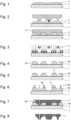
- the substrate 1 used in step a) of the method according to the inventionis, for example, formed by a silicon substrate.
- a first conductive layer 2is deposited, for example, by physical vapor deposition (PVD), that is to say a layer capable of starting a metal deposition by galvanic means.
- PVDphysical vapor deposition
- the first conductive layer 2is of the Au, Ti, Pt, Ag, Cr or Pd type ( figure 1 ), or a stack of at least two of these materials, and has a thickness of between 50nm and 500nm.
- the first conductive layer 2can be formed from a sub-layer of chromium or titanium covered with a layer of gold or copper.
- the photosensitive resin 3 used in this processis preferably an octofunctional epoxy-based negative type resin such as SU-8 resin designed to polymerize under the action of UV radiation.
- the photosensitive resin 3can be in the form of a dry film, the resin is then applied by lamination to the substrate 1.
- the photoresistcould be a positive photoresist which is designed to decompose under the action of UV radiation. It will be understood that the present invention is not limited to a few particular types of photosensitive resin. Those skilled in the art will be able to choose a photosensitive resin suitable for their needs from among all the known resins which are suitable for UV photolithography.
- the first layer of resin 3is deposited on the substrate 1 by any appropriate means, by centrifugal coating, by spinning, or by spraying until the desired thickness.
- the resin thicknessis between 10 ⁇ m and 1000 ⁇ m, and preferably between 30 ⁇ m and 300 ⁇ m.
- the first layer of resin 3will be deposited in one or more times.
- the first layer of resin 3is then heated typically between 90 and 120° C for a period depending on the thickness deposited. to evacuate the solvent (pre-bake step). This heating dries and hardens the resin.
- the following step b) illustrated in figure 2consists of hot stamping the first layer of resin 3 to shape it and define a first level of the watch component.
- the resinis initially heated to a temperature between 70°C and 150°C where it becomes viscous to allow it to be shaped by crushing it using a pad 8 which presses it.
- This stepcan be carried out under vacuum to avoid the formation of air bubbles during pressing of the resin layer 3.
- the pad 8is pressed until completely crushed, up to the substrate 1 so that Only a residual film of resin remains above the conductive layer where the pad parts have been pressed against the substrate.
- the pad 8has a relief imprint which can have variations in height and thus makes it possible to define at least one first level of the component, said at least first level thus has a complex three-dimensional geometry which it is not possible to obtained by a classic LIGA process.
- step c) illustrated in Figure 3consists of irradiating the first layer of resin 3 by means of UV radiation through a mask 4 defining the first level of the component to be formed and thus photopolymerized zones 3a and non-photopolymerized zones 3b.
- This stepensures that the residual film of resin remaining after pressing the pad disappears to reveal the conductive layer, and allows the resin to be structured as usually carried out in LIGA.
- An annealing step (post-bake step) of the first resin layer 3may be necessary to complete the photopolymerization induced by UV irradiation. This annealing step is preferably carried out between 90°C and 95°C.
- the photopolymerized zones 3abecome insensitive to a large majority of solvents.
- the non-photopolymerized areascan subsequently be dissolved by a solvent.
- the non-photopolymerized zones 3b of the first layer 3 of photosensitive resinare dissolved to reveal in places the first conductive layer 2 of the substrate 1 as on the Figure 4 .
- This operationis carried out by dissolving the non-photopolymerized zones 3b using a suitable solvent, such as PGMEA (propylene glycol methyl ethyl acetate).
- PGMEApropylene glycol methyl ethyl acetate
- a second conductive layer 5is deposited on the photopolymerized zones 3a during the previous step.
- This second conductive layer 5may have the same characteristics as the first conductive layer 2, namely that it is of the Au, Ti, Pt, Ag, Cr, Pd type or a stack of at least two of these materials, and has a thickness between 50nm and 500nm.
- a template maskis used which is positioned via optical alignment.
- Such equipmentmakes it possible to guarantee good alignment of the mask with the geometry of the photopolymerized zones 3a on the substrate and thus guarantee a deposition only on the upper surface of the photopolymerized zones 3a while avoiding a deposit on the sides of the photopolymerized resin 3a because the mask is kept as close as possible to substrate 1.
- the second electrically conductive layeris implemented by global deposition on all the exposed surfaces (sidewalls included) then removed entirely except on the upper surface of the first layer of resin, where it was protected by means of a saving deposited by stamping.
- step e) illustrated in Figure 6consists of depositing a second layer 6 of photosensitive resin covering the structure resulting from the previous step.
- the same resinis used during this step, and the thickness is greater than that deposited during step a).
- the thicknessvaries depending on the geometry of the component that we wish to obtain.
- the continuationconsists of irradiating the second layer 6 of resin through a 4" mask defining a second level of the component and dissolving the non-irradiated zones 6b of the second layer 6 of photosensitive resin.
- a moldcomprising a first and a second level revealing in places the first electrically conductive layer 2 and the second electrically conductive layer 5.
- the following step f) illustrated in Figure 7consists of depositing in the mold, by electroforming or galvanic deposition, a layer 7 of a metal from the first layer 2 and possible second electrically conductive layer 5 until forming a block preferably reaching a height less than the height of the mold, this allows for better mechanical strength during subsequent machining.
- metalin this context are of course understood metal alloys.
- the metalwill be chosen from the set comprising nickel, copper, gold or silver, and, as alloy, gold-copper, nickel-cobalt, nickel-iron, nickel-phosphorus, or even nickel-tungsten.
- the multi-layer metal structureis made entirely of the same alloy or metal. However, it is also possible to change the metal or alloy during the galvanic deposition step so as to obtain a metallic structure comprising at least two layers of different natures.
- the electroforming conditionsin particular the composition of the baths, the geometry of the system, the voltages and current densities, are chosen for each metal or alloy to be electroplated according to techniques well known in the art of electroforming.
- the metal layer 7can be machined by a mechanical process so as to obtain a thickness predefined by the thickness of the component to be produced. Depending on the side on which this operation must be carried out, the recovery can be done in wafer.
- Step g)consists of releasing the component by eliminating, through a succession of wet or dry etching steps, the substrate, the conductive layers or the resin layers, operations familiar to those skilled in the art.
- the first conductive layer 2 and the substrate 1are removed by means of wet etching, which makes it possible to release the component from the substrate 1 without damaging it.
- the silicon substratecan be etched with a potassium hydroxide (KOH) solution.
- a second sequenceconsists of eliminating the first layer 3 and the second layer 6 of resin by means of O 2 plasma etchings, spaced between wet etchings of the intermediate metal layers.
- the components obtainedcan be cleaned, and possibly taken back to a machine tool to carry out machining or aesthetic finishing.
- the partscan be directly used or subjected to various decorative and/or functional treatments, typically physical or chemical deposits.
- the process of the inventionfinds a particularly advantageous application for the manufacture of components for timepieces, such as springs, anchors, wheels, brackets, etc. Thanks to this process, it is possible to produce components of more diverse shapes and presenting complex geometries than those obtained via conventional photolithography operations. Such a process also makes it possible to obtain robust components which have good reliability in terms of geometries.
Landscapes
- Chemical & Material Sciences (AREA)
- Physics & Mathematics (AREA)
- General Physics & Mathematics (AREA)
- Engineering & Computer Science (AREA)
- Metallurgy (AREA)
- Organic Chemistry (AREA)
- Materials Engineering (AREA)
- Chemical Kinetics & Catalysis (AREA)
- Electrochemistry (AREA)
- Crystallography & Structural Chemistry (AREA)
- Mechanical Engineering (AREA)
- Optics & Photonics (AREA)
- Plasma & Fusion (AREA)
- Manufacturing & Machinery (AREA)
- Microelectronics & Electronic Packaging (AREA)
- Inorganic Chemistry (AREA)
- Micromachines (AREA)
- Moulds For Moulding Plastics Or The Like (AREA)
- Manufacturing Of Printed Wiring (AREA)
- Photosensitive Polymer And Photoresist Processing (AREA)
- Shaping Of Tube Ends By Bending Or Straightening (AREA)
Description
Translated fromFrenchLa présente invention concerne un procédé de fabrication d'une structure métallique complexe multi-niveaux au moyen de la technologie LIGA. L'invention concerne également une telle structure métallique, notamment des composants horlogers, obtenus par ce procédé.The present invention relates to a method for manufacturing a complex multi-level metal structure using LIGA technology. The invention also relates to such a metallic structure, in particular watch components, obtained by this process.
On connaît déjà des procédés correspondant à la définition ci-dessus. En particulier, l'article d'
- créer sur un substrat une couche métallique sacrificielle et une couche d'amorçage pour une étape ultérieure de croissance galvanique,
- étaler une couche de polyimide photosensible,
- irradier la couche de polyimide avec un rayonnement UV à travers un masque correspondant au contour d'un niveau de la structure à obtenir,
- développer la couche de polyimide en dissolvant les parties non irradiées de façon à obtenir un moule en polyimide,
- remplir le moule de nickel jusqu'à la hauteur de celui-ci par croissance galvanique, et obtenir une surface supérieure sensiblement plane,
- déposer une fine couche de chrome sur toute la surface supérieure par vaporisation sous vide,
- déposer sur la couche de chrome une nouvelle couche de résine photosensible,
- irradier la couche de résine à travers un nouveau masque correspondant au contour du niveau suivant de la structure à obtenir,
- développer la couche de polyimide de façon à obtenir un nouveau moule,
- remplir le nouveau moule de nickel jusqu'à la hauteur de celui-ci par croissance galvanique.
- séparer la structure multi-niveaux et le moule en polyimide de la couche sacrificielle et du substrat,
- séparer la structure multi-niveaux du moule en polyimide.
- create on a substrate a sacrificial metal layer and a priming layer for a subsequent galvanic growth step,
- spread a layer of photosensitive polyimide,
- irradiate the polyimide layer with UV radiation through a mask corresponding to the contour of a level of the structure to be obtained,
- develop the polyimide layer by dissolving the non-irradiated parts so as to obtain a polyimide mold,
- fill the mold with nickel up to the height thereof by galvanic growth, and obtain a substantially flat upper surface,
- deposit a thin layer of chrome over the entire upper surface by vacuum vaporization,
- deposit a new layer of photosensitive resin on the chrome layer,
- irradiate the resin layer through a new mask corresponding to the contour of the next level of the structure to obtain,
- develop the polyimide layer so as to obtain a new mold,
- fill the new mold with nickel up to the height of it by galvanic growth.
- separate the multi-level structure and the polyimide mold from the sacrificial layer and the substrate,
- separate the multi-level structure from the polyimide mold.
On comprendra que le procédé qui vient d'être décrit peut, en principe, être mis en oeuvre de manière itérative pour obtenir des structures métalliques ayant plus de deux niveaux.It will be understood that the process which has just been described can, in principle, be implemented iteratively to obtain metallic structures having more than two levels.
Le document de brevet
On connait également du document de brevet
Ces procédés ne permettent que la fabrication de pièces dont leurs géométries de base sont cylindriques, et ne permettent pas la fabrication de pièces comprenant des géométries complexes telles que des anglages ou des chanfreins.These processes only allow the manufacture of parts whose basic geometries are cylindrical, and do not allow the manufacture of parts comprising complex geometries such as bevels or chamfers.
La demande de brevet
La présente invention a pour but de remédier aux inconvénients susmentionnés ainsi qu'à d'autres encore en fournissant un procédé permettant de fabriquer des composants horlogers métalliques multi-niveaux, en combinant une étape d'emboutissage à chaud à la technologie LIGA, dans lequel une couche conductrice est associée à une couche de résine pour chaque niveau pour permettre une croissance galvanique fiable dans le cas de composants multiniveaux.The present invention aims to remedy the aforementioned drawbacks as well as others by providing a process making it possible to manufacture multi-level metallic watch components, by combining a hot stamping step with LIGA technology, in which a conductive layer is associated with a resin layer for each level to enable reliable galvanic growth in the case of multilevel components.
La présente invention a également pour but de permettre la fabrication de pièces horlogères présentant des géométries complexes d'ordinaire infaisable via la technologie LIGA.The present invention also aims to enable the manufacture of watch parts having complex geometries that are ordinarily infeasible via LIGA technology.
A cet effet l'invention a pour objet un procédé de fabrication d'un composant horloger comprenant les étapes suivantes :
- a) se munir d'un substrat, y déposer une première couche électriquement conductrice, et appliquer une première couche de résine photosensible ;
- b) effectuer un emboutissage à chaud via un tampon de la première couche de résine photosensible, en pressant le tampon jusqu'au substrat, pour la mettre en forme et définir un premier niveau du composant horloger ;
- c) irradier la première couche de résine photosensible mise en forme à travers un masque définissant un premier niveau du composant horloger et dissoudre les zones non irradiées de la couche de résine photosensible pour faire apparaître par endroit la première couche électriquement conductrice ;
- e) appliquer une deuxième couche de résine photosensible recouvrant la structure résultant de l'étape c), puis irradier la deuxième couche de résine photosensible à travers un masque définissant un deuxième niveau du composant et dissoudre les zones non irradiées de la deuxième couche de résine photosensible pour former un moule comprenant un premier et un second niveau ;
- f) déposer une couche métallique par électroformage dans le moule à partir de la première couche électriquement conductrice pour former le composant horloger, la couche métallique atteignant sensiblement la surface supérieure de la deuxième couche de résine photosensible ;
- g) éliminer successivement le substrat, la première couche électriquement conductrice et la résine photosensible pour libérer le composant horloger.
- a) provide a substrate, deposit a first electrically conductive layer on it, and apply a first layer of photosensitive resin;
- b) perform hot stamping via a pad of the first layer of photosensitive resin, by pressing the pad up to the substrate, to shape it and define a first level of the watch component;
- c) irradiate the first layer of shaped photosensitive resin through a mask defining a first level of the watch component and dissolve the non-irradiated areas of the layer of photosensitive resin to reveal the first electrically conductive layer in places;
- e) apply a second layer of photosensitive resin covering the structure resulting from step c), then irradiate the second layer of photosensitive resin through a mask defining a second level of the component and dissolve the non-irradiated areas of the second layer of resin photosensitive to form a mold comprising a first and a second level;
- f) deposit a metallic layer by electroforming in the mold from the first electrically conductive layer to form the watch component, the metal layer substantially reaching the upper surface of the second photosensitive resin layer;
- g) successively eliminate the substrate, the first electrically conductive layer and the photosensitive resin to release the watch component.
Ce procédé permet donc la réalisation de pièces multiniveaux.This process therefore allows the production of multilevel parts.
Conformément à d'autres variantes avantageuses de l'invention :
- l'étape b) est réalisée sous vide.
- lors de l'étape b), la première couche de résine photosensible est chauffée entre 70°C et 150°C ;
- le tampon présente une empreinte en relief, au moins une partie de l'empreinte étant agencée pour être pressée directement contre la surface du substrat lors de l'étape b) ;
- ladite empreinte du tampon définit ledit au moins un premier niveau du composant horloger;
- le procédé comprend une étape optionnelle d'), à la suite de l'étape c), qui consiste à déposer localement une deuxième couche électriquement conductrice sur les zones irradiées de la première couche de résine photosensible;
- la deuxième couche électriquement conductrice est déposée à travers un masque chablon ;
- la deuxième couche électriquement conductrice est mise en oeuvre par dépôt global sur toutes les surfaces exposées (flancs compris) puis retirée intégralement sauf sur la surface supérieure de la première couche de résine photosensible, où elle a été protégée au moyen d'une épargne déposée par tamponnage ;
- la deuxième couche électriquement conductrice est déposée via l'impression d'une encre ou d'une résine conductrice ;
- ladite première couche et ladite deuxième couche électriquement conductrice sont du type Au, Ti, Pt, Ag, Cr, Pd ou un empilement d'au moins deux de ces matériaux ;
- le substrat est en silicium ;
- la première couche conductrice présente une épaisseur comprise entre 50nm et 500nm ;
- la deuxième couche conductrice présente une épaisseur comprise entre 50nm et 500nm.
- step b) is carried out under vacuum.
- during step b), the first layer of photosensitive resin is heated between 70°C and 150°C;
- the stamp has a raised imprint, at least part of the imprint being arranged to be pressed directly against the surface of the substrate during step b);
- said buffer imprint defines said at least one first level of the watch component;
- the method comprises an optional step d'), following step c), which consists of locally depositing a second electrically conductive layer on the irradiated areas of the first layer of photosensitive resin;
- the second electrically conductive layer is deposited through a stencil mask;
- the second electrically conductive layer is implemented by global deposition on all exposed surfaces (sidewalls included) then removed entirely except on the upper surface of the first layer of photosensitive resin, where it was protected by means of a saving deposited by stamping;
- the second electrically conductive layer is deposited via printing an ink or a conductive resin;
- said first layer and said second electrically conductive layer are of the Au, Ti, Pt, Ag, Cr, Pd type or a stack of at least two of these materials;
- the substrate is made of silicon;
- the first conductive layer has a thickness of between 50nm and 500nm;
- the second conductive layer has a thickness of between 50nm and 500nm.
L'invention a également pour objet un procédé de fabrication d'un composant horloger selon la revendication 2, des modes de réalisation particuliers étant définis par les revendications 3, 4 et 7 à 14, dans la mesure où ces dernières dépendent de la revendication 2.The invention also relates to a method of manufacturing a watch component according to
Enfin, l'invention se rapporte à un composant horloger, obtenu selon un procédé conforme à l'invention, tel qu'une ancre ou une roue d'échappement par exemple.Finally, the invention relates to a watch component, obtained according to a process according to the invention, such as an anchor or an escape wheel for example.
On comprend donc que le procédé de l'invention trouve une application particulièrement avantageuse pour la fabrication de composants pour les pièces d'horlogerie.We therefore understand that the process of the invention finds a particularly advantageous application for the manufacture of components for timepieces.
D'autres caractéristiques et avantages de la présente invention ressortiront plus clairement de la description détaillée qui suit d'un exemple de réalisation d'un procédé selon l'invention, cet exemple étant donné seulement à titre purement illustratif et non limitatif, en liaison avec le dessin annexé sur lequel :
- les
figures 1 à 8 illustrent les étapes de procédé d'un mode de réalisation de l'invention en vue de la réalisation d'un composant horloger.
- THE
figures 1 to 8 illustrate the process steps of an embodiment of the invention with a view to producing a watch component.
Le substrat 1 utilisé dans l'étape a) du procédé selon l'invention est, par exemple, formé par un substrat en silicium. Lors de la première étape a) du procédé on dépose, par exemple, par un dépôt physique en phase vapeur (PVD), une première couche conductrice 2, c'est-à-dire une couche apte à démarrer un dépôt métallique par voie galvanique. Typiquement, la première couche conductrice 2 est du type Au, Ti, Pt, Ag, Cr ou Pd (
La résine photosensible 3 utilisée dans ce procédé est de préférence une résine de type négative à base d'époxy octofonctionnelle telle que la résine SU-8 conçue pour polymériser sous l'action d'un rayonnement UV.The
La résine photosensible 3 peut se présenter sous la forme d'un film sec, la résine est alors appliquée par laminage sur le substrat 1.The
Alternativement, la résine photosensible pourrait être un photorésist positif qui est conçu pour se décomposer sous l'action d'un rayonnement UV. On comprendra que la présente invention ne se limite pas à quelques types particuliers de résine photosensible. L'homme du métier saura choisir une résine photosensible convenant à ses besoins parmi toutes les résines connues qui sont adaptées à la photolithographie par UV.Alternatively, the photoresist could be a positive photoresist which is designed to decompose under the action of UV radiation. It will be understood that the present invention is not limited to a few particular types of photosensitive resin. Those skilled in the art will be able to choose a photosensitive resin suitable for their needs from among all the known resins which are suitable for UV photolithography.
La première couche de résine 3 est déposée sur le substrat 1 par tout moyen approprié, par enduction centrifuge, à la tournette, ou encore par sprayage jusqu'à l'épaisseur souhaitée. Typiquement l'épaisseur de résine est comprise entre 10 µm et 1000 µm, et de préférence entre 30 µm et 300 µm. Selon l'épaisseur désirée et la technique de dépôt utilisée la première couche de résine 3 sera déposée en une ou plusieurs fois.The first layer of
La première couche de résine 3 est ensuite chauffée typiquement entre 90 et 120° C pendant une durée dépendant de l'épaisseur déposée pour évacuer le solvant (étape de pre-bake). Ce chauffage sèche et durcit la résine.The first layer of
L'étape b) suivante illustrée à la
Avantageusement, le tampon 8 présente une empreinte en relief pouvant présenter des variations de hauteur et permettant ainsi de définir au moins un premier niveau du composant, ledit au moins premier niveau présente ainsi une géométrie tridimensionnelle complexe qu'il n'est pas possible d'obtenir par un procédé LIGA classique.Advantageously, the
Il peut également être envisagé de former deux niveaux ou plus au moyen du tampon.It can also be envisaged to form two or more levels using the buffer.
L'étape c) suivante illustrée à la
Cette étape permet de garantir que le film résiduel de résine restant après le pressage du tampon disparaît pour faire apparaître la couche conductrice, et permet de structurer la résine comme effectué usuellement en LIGA.This step ensures that the residual film of resin remaining after pressing the pad disappears to reveal the conductive layer, and allows the resin to be structured as usually carried out in LIGA.
Une étape de recuit (étape de post-bake) de la première couche de résine 3 peut être nécessaire pour compléter la photopolymérisation induite par l'irradiation UV. Cette étape de recuit est effectuée de préférence entre 90°C et 95°C. Les zones photopolymérisées 3a deviennent insensibles à une grande majorité de solvants. Par contre, les zones non photopolymérisées pourront ultérieurement être dissoutes par un solvant.An annealing step (post-bake step) of the
Ensuite, on dissout les zones non photopolymérisées 3b de la première couche 3 de résine photosensible pour faire apparaître par endroit la première couche conductrice 2 du substrat 1 comme sur la
Selon une étape d') optionnelle illustrée à la
Selon une première variante de l'invention, on utilise un masque chablon qui est positionné via un alignement optique. Un tel équipement permet de garantir un bon alignement du masque avec la géométrie des zones photopolymérisées 3a sur le substrat et ainsi garantir un dépôt uniquement sur la surface supérieure des zones photopolymérisées 3a tout en évitant un dépôt sur les flancs de la résine photopolymérisées 3a car le masque est maintenu au plus proche du substrat 1.According to a first variant of the invention, a template mask is used which is positioned via optical alignment. Such equipment makes it possible to guarantee good alignment of the mask with the geometry of the
Selon une deuxième variante de l'invention, la deuxième couche électriquement conductrice est mise en oeuvre par dépôt global sur toutes les surfaces exposées (flancs compris) puis retirée intégralement sauf sur la surface supérieure de la première couche de résine, où elle a été protégée au moyen d'une épargne déposée par tamponnage.According to a second variant of the invention, the second electrically conductive layer is implemented by global deposition on all the exposed surfaces (sidewalls included) then removed entirely except on the upper surface of the first layer of resin, where it was protected by means of a saving deposited by stamping.
L'homme du métier pourrait également envisager la mise en oeuvre d'une impression 3D pour déposer la deuxième couche conductrice 5.Those skilled in the art could also consider implementing 3D printing to deposit the second
De telles solutions permettent un dépôt sélectif et plus précis de la deuxième couche électriquement conductrice 5, et donc de n'avoir aucun dépôt sur les flancs de la résine photopolymérisées 3a.Such solutions allow selective and more precise deposition of the second electrically
L'étape e) suivante illustrée à la
La suite consiste à irradier la deuxième couche 6 de résine à travers un masque 4" définissant un deuxième niveau du composant et dissoudre les zones 6b non irradiées de la deuxième couche 6 de résine photosensible. A la fin de cette étape (
L'étape f) suivante illustrée à la
Les conditions d'électroformage, notamment la composition des bains, la géométrie du système, les tensions et densités de courant, sont choisis pour chaque métal ou alliage à électrodéposer selon les techniques bien connues dans l'art de l'électroformage.The electroforming conditions, in particular the composition of the baths, the geometry of the system, the voltages and current densities, are chosen for each metal or alloy to be electroplated according to techniques well known in the art of electroforming.
La couche métallique 7 peut être usinée par un procédé mécanique de manière à obtenir une épaisseur prédéfinie par l'épaisseur du composant à réaliser. Selon la face sur laquelle cette opération doit être effectuée, la reprise peut être faite en wafer.The
L'étape g) consiste à libérer le composant en éliminant par une succession d'étapes de gravure, humide ou sèche, le substrat, les couches conductrices ou les couches de résine, opérations familières à l'homme du métier. Par exemple la première couche conductrice 2 et le substrat 1 sont éliminés au moyen d'une gravure humide, ce qui permet de libérer le composant du substrat 1 sans l'endommager. Notoirement, le substrat en silicium peut être gravé avec une solution à base d'hydroxyde de potassium (KOH).Step g) consists of releasing the component by eliminating, through a succession of wet or dry etching steps, the substrate, the conductive layers or the resin layers, operations familiar to those skilled in the art. For example, the first
A l'issue de cette première séquence, on obtient un composant pris dans les première et deuxième couches de résine, la deuxième couche conductrice 5 étant également encore présente par endroit.At the end of this first sequence, we obtain a component taken from the first and second resin layers, the second
Une deuxième séquence consiste à éliminer la première couche 3 et la deuxième couche 6 de résine au moyen de gravures plasma O2, espacées de gravures humides des couches métalliques intermédiaires.A second sequence consists of eliminating the
A l'issue de cette étape, les composants obtenus peuvent être nettoyés, et éventuellement repris sur une machine-outil pour opérer des usinages ou une terminaison esthétique. A ce stade, les pièces peuvent être directement utilisées ou bien soumises à divers traitements décoratifs et/ou fonctionnels, typiquement des dépôts physiques ou chimiques.At the end of this step, the components obtained can be cleaned, and possibly taken back to a machine tool to carry out machining or aesthetic finishing. At this stage, the parts can be directly used or subjected to various decorative and/or functional treatments, typically physical or chemical deposits.
Le procédé de l'invention trouve une application particulièrement avantageuse pour la fabrication de composants pour pièces d'horlogerie, tels que des ressorts, des ancres, des roues, des appliques, etc. Grâce à ce procédé, on peut réaliser des composants de forme plus diverses et présentant des géométries complexes que ceux obtenus via des opérations de photolithographie classiques. Un tel procédé permet également d'obtenir des composants robustes et qui présentent une bonne fiabilité au niveau des géométries.The process of the invention finds a particularly advantageous application for the manufacture of components for timepieces, such as springs, anchors, wheels, brackets, etc. Thanks to this process, it is possible to produce components of more diverse shapes and presenting complex geometries than those obtained via conventional photolithography operations. Such a process also makes it possible to obtain robust components which have good reliability in terms of geometries.
Claims (14)
- Method for manufacturing at least one timepiece component comprising the following steps of:a) providing a substrate (1), depositing a first electrically conductive layer (2) thereon and applying a first photoresist layer (3);b) hot-pressing the first photoresist layer (3) using a stamp (8), by pressing the stamp (8) down as far as the substrate, in order to shape the first photoresist layer and define a first level of the timepiece component;c) irradiating the first shaped photoresist layer (3) through a mask (4) defining the at least one first level of the timepiece component and dissolving the non-irradiated areas (3b) of the first photoresist layer (3) to reveal, in places, the first electrically conductive layer (2);d) applying a second photoresist layer (6) covering the structure produced in step c), then irradiating the second photoresist layer (6) through a mask (4") defining a second level of the timepiece component and dissolving the non-irradiated areas (6b) of the second photoresist layer (6) to form a mould comprising a first and a second level;e) depositing a metal layer (7) in the mould by electroforming from the first electrically conductive layer (2) to form the timepiece component, the metal layer (7) substantially reaching the upper surface of the second photoresist layer (6);f) successively removing the substrate, the first electrically conductive layer (2) and the first and second photoresist layers (3, 6) to release the timepiece component.
- Method for manufacturing at least one timepiece component comprising the following steps of:a') providing a substrate (1), depositing a first electrically conductive layer (2) thereon and applying a first photoresist layer (3);b') irradiating the first photoresist layer (3) through a first mask (4) defining at least a first level of the timepiece component and dissolving the non-irradiated areas (3b) of the photoresist layer (3) to reveal, in places, the first electrically conductive layer (2);c') applying a second photoresist layer (6) covering the structure produced in step c),d') hot-pressing the second photoresist layer (6) using a stamp to shape the second photoresist layer (6) and define a second level of the timepiece component;e') irradiating the second shaped photoresist layer (6) through a second mask (4") defining the second level of the timepiece component and dissolving the non-irradiated areas (6b) of the second photoresist layer (6) to form a mould comprising the first level and the second level;f') depositing a metal layer (7) in the mould by electroforming from the first electrically conductive layer (2) to form the component, the metal layer (7) substantially reaching the upper surface of the second photoresist layer (6);g') successively removing the substrate, the first electrically conductive layer (2) and the first and second photoresist layers (3, 6) to release the timepiece component.
- Method according to claim 1 or 2,characterised in that step b) or step d') is carried out in a vacuum.
- Method according to claim 1 or 2,characterised in that in step b) or step d'), the first photoresist layer is heated to between 70°C and 150°C.
- Method according to any of claims 1, 3 or 4,characterised in that the stamp has a raised impression, at least part of the impression being arranged to be pressed directly against the surface of the substrate in step b).
- Method according to claim 5,characterised in that said impression of the stamp defines said at least one first level of the timepiece component.
- Method according to claim 1 or 2,characterised in that it comprises an optional step d'), after step c) or step b'), which consists in locally depositing a second electrically conductive layer (5) on the irradiated areas (3a) of the first photoresist layer (3).
- Method according to claim 7,characterised in that the second electrically conductive layer (5) is deposited through a stencil mask (4').
- Method according to claim 7,characterised in that in step d'), the second electrically conductive layer (5) is applied by comprehensive deposition on all the exposed surfaces, including the sidewalls, and then is entirely removed except from the upper surface of the first photoresist layer, where it was protected by means of a resist deposited by stamping.
- Method according to claim 7,characterised in that in step d'), the second electrically conductive layer (5) is deposited by printing an ink or a conductive resin.
- Method according to any of the preceding claims,characterised in that said first electrically conductive layer (2) and said second electrically conductive layer (5) are of the Au, Ti, Pt, Ag, Cr or Pd type.
- Method according to any of the preceding claims,characterised in that the substrate (1) is made of silicon.
- Method according to any of the preceding claims,characterised in that the first electrically conductive layer (2) has a thickness comprised between 50 nm and 500 nm.
- Method according to any of the preceding claims,characterised in that the second electrically conductive layer (5) has a thickness comprised between 50 nm and 500 nm.
Priority Applications (6)
| Application Number | Priority Date | Filing Date | Title |
|---|---|---|---|
| EP19217376.3AEP3839626B1 (en) | 2019-12-18 | 2019-12-18 | Method for manufacturing a timepiece component |
| TW109143033ATWI833053B (en) | 2019-12-18 | 2020-12-07 | Method of fabricating a timepiece component and component obtained from this method |
| KR1020200173699AKR102520739B1 (en) | 2019-12-18 | 2020-12-11 | Method of fabricating a timepiece component and component obtained from this method |
| JP2020205533AJP7112472B2 (en) | 2019-12-18 | 2020-12-11 | Method for making timepiece components and components resulting from this method |
| US17/121,095US12124223B2 (en) | 2019-12-18 | 2020-12-14 | Method of fabricating a timepiece component and component obtained from this method |
| CN202011500852.9ACN113009780B (en) | 2019-12-18 | 2020-12-18 | Method for manufacturing a timepiece component and component obtained by this method |
Applications Claiming Priority (1)
| Application Number | Priority Date | Filing Date | Title |
|---|---|---|---|
| EP19217376.3AEP3839626B1 (en) | 2019-12-18 | 2019-12-18 | Method for manufacturing a timepiece component |
Publications (2)
| Publication Number | Publication Date |
|---|---|
| EP3839626A1 EP3839626A1 (en) | 2021-06-23 |
| EP3839626B1true EP3839626B1 (en) | 2023-10-11 |
Family
ID=68944553
Family Applications (1)
| Application Number | Title | Priority Date | Filing Date |
|---|---|---|---|
| EP19217376.3AActiveEP3839626B1 (en) | 2019-12-18 | 2019-12-18 | Method for manufacturing a timepiece component |
Country Status (6)
| Country | Link |
|---|---|
| US (1) | US12124223B2 (en) |
| EP (1) | EP3839626B1 (en) |
| JP (1) | JP7112472B2 (en) |
| KR (1) | KR102520739B1 (en) |
| CN (1) | CN113009780B (en) |
| TW (1) | TWI833053B (en) |
Families Citing this family (3)
| Publication number | Priority date | Publication date | Assignee | Title |
|---|---|---|---|---|
| EP3839625A1 (en) | 2019-12-18 | 2021-06-23 | Nivarox-FAR S.A. | Method for manufacturing a timepiece component and component produced by this method |
| EP3839624B1 (en)* | 2019-12-18 | 2023-09-13 | Nivarox-FAR S.A. | Method for manufacturing a timepiece component |
| EP4546059A1 (en)* | 2023-10-26 | 2025-04-30 | The Swatch Group Research and Development Ltd | Method for obtaining an article with a glittering polycrystalline surface |
Citations (1)
| Publication number | Priority date | Publication date | Assignee | Title |
|---|---|---|---|---|
| JP2006161138A (en)* | 2004-12-10 | 2006-06-22 | Seiko Instruments Inc | Electroforming die and its production method |
Family Cites Families (33)
| Publication number | Priority date | Publication date | Assignee | Title |
|---|---|---|---|---|
| JPS4844138A (en)* | 1971-06-15 | 1973-06-25 | ||
| CN1112361A (en)* | 1993-06-08 | 1995-11-22 | 精工爱普生株式会社 | Mold for duplication of concave-convex pattern and method for duplicating concave-convex pattern |
| EP1015669B1 (en)* | 1997-04-04 | 2010-11-17 | University Of Southern California | Electroplating method for forming a multilayer structure |
| US6245849B1 (en)* | 1999-06-02 | 2001-06-12 | Sandia Corporation | Fabrication of ceramic microstructures from polymer compositions containing ceramic nanoparticles |
| US20020045028A1 (en)* | 2000-10-10 | 2002-04-18 | Takayuki Teshima | Microstructure array, mold for forming a microstructure array, and method of fabricating the same |
| WO2004065660A1 (en)* | 2003-01-17 | 2004-08-05 | Toppan Printing Co., Ltd. | Metal photo-etching product and production method therefor |
| JP4383182B2 (en)* | 2003-07-11 | 2009-12-16 | 株式会社クラレ | Manufacturing method of stamper for resin molded product and manufacturing method for resin molded product |
| JP2006299371A (en)* | 2005-04-25 | 2006-11-02 | Ricoh Elemex Corp | Method for producing fine metal structure, and fine metal structure |
| FR2903679B1 (en)* | 2006-07-17 | 2014-07-04 | Centre Nat Rech Scient | MANUFACTURE OF POLYMERIC MICROFLUIDIC DEVICES BY PHOTO-ASSISTED PRINTING |
| JP5030618B2 (en) | 2007-02-27 | 2012-09-19 | セイコーインスツル株式会社 | Electroforming mold and manufacturing method thereof |
| JP4825785B2 (en)* | 2007-12-20 | 2011-11-30 | 三菱製紙株式会社 | Method for producing mask for screen printing with steps |
| CH704572B1 (en)* | 2007-12-31 | 2012-09-14 | Nivarox Sa | A method of manufacturing a metal microstructure and microstructure obtained using this method. |
| EP2105807B1 (en)* | 2008-03-28 | 2015-12-02 | Montres Breguet SA | Monobloc elevated curve spiral and method for manufacturing same |
| EP2157476A1 (en)* | 2008-08-20 | 2010-02-24 | Nivarox-FAR S.A. | Method of manufacturing multi-level metal parts using the LIGA-UV technique |
| JP5470791B2 (en)* | 2008-09-29 | 2014-04-16 | オムロン株式会社 | Electroforming method |
| EP2182096A1 (en)* | 2008-10-28 | 2010-05-05 | Nivarox-FAR S.A. | Heterogeneous LIGA method |
| CN102712110B (en)* | 2009-09-03 | 2015-07-22 | Lg电子株式会社 | Method of manufacturing master mold for forming micropattern film applied to exterior of home appliance, and film manufacturing apparatus and method using master mold |
| EP2405300A1 (en)* | 2010-07-09 | 2012-01-11 | Mimotec S.A. | Manufacturing method for multi-level metal parts through an LIGA type method and parts obtained using the method |
| CN103068556B (en)* | 2010-08-06 | 2015-07-22 | 综研化学株式会社 | Resin mold for nanoimprinting and manufacturing method thereof |
| EP2823357B1 (en)* | 2012-03-09 | 2016-03-02 | Danmarks Tekniske Universitet | A method for manufacturing a tool part for an injection molding process, a hot embossing process, a nano-imprint process, or an extrusion process |
| CH706621A1 (en)* | 2012-06-05 | 2013-12-13 | Mimotec Sa | Manufacturing process difficult to reproduce micromechanical parts, and micromechanical parts made by this process. |
| CN102746033B (en) | 2012-06-10 | 2014-03-12 | 无锡赛雅环保科技有限公司 | Mobile distributed treatment method and device for kitchen garbage |
| JP6239300B2 (en)* | 2013-07-25 | 2017-11-29 | セイコーインスツル株式会社 | Timepiece parts manufacturing method, timepiece parts, movement and timepiece |
| EP3035125B1 (en)* | 2014-12-19 | 2018-01-10 | Rolex Sa | Method for manufacturing a multi-level clock component |
| JP6434833B2 (en) | 2015-03-18 | 2018-12-05 | セイコーインスツル株式会社 | Electroforming mold, electroforming mold and electroforming mold manufacturing method |
| EP3202708B1 (en)* | 2016-02-03 | 2023-05-03 | Rolex Sa | Method for manufacturing a hybrid clock component |
| HK1220859A2 (en)* | 2016-02-29 | 2017-05-12 | Master Dynamic Limited | Liga fabrication process |
| EP3266905B1 (en) | 2016-07-04 | 2020-05-13 | Richemont International S.A. | Method for manufacturing a timepiece component |
| IL267443B2 (en)* | 2016-12-22 | 2023-10-01 | Illumina Inc | stamping device |
| KR102436152B1 (en)* | 2017-10-27 | 2022-08-25 | 주식회사 엘지화학 | Imprinting mold and manufacturing method for imprinting mold |
| CH714739A2 (en)* | 2018-03-09 | 2019-09-13 | Swatch Group Res & Dev Ltd | Method of manufacturing a metallic decoration on a dial and dial obtained according to this method. |
| EP3839625A1 (en) | 2019-12-18 | 2021-06-23 | Nivarox-FAR S.A. | Method for manufacturing a timepiece component and component produced by this method |
| EP3839624B1 (en) | 2019-12-18 | 2023-09-13 | Nivarox-FAR S.A. | Method for manufacturing a timepiece component |
- 2019
- 2019-12-18EPEP19217376.3Apatent/EP3839626B1/enactiveActive
- 2020
- 2020-12-07TWTW109143033Apatent/TWI833053B/enactive
- 2020-12-11JPJP2020205533Apatent/JP7112472B2/enactiveActive
- 2020-12-11KRKR1020200173699Apatent/KR102520739B1/enactiveActive
- 2020-12-14USUS17/121,095patent/US12124223B2/enactiveActive
- 2020-12-18CNCN202011500852.9Apatent/CN113009780B/enactiveActive
Patent Citations (1)
| Publication number | Priority date | Publication date | Assignee | Title |
|---|---|---|---|---|
| JP2006161138A (en)* | 2004-12-10 | 2006-06-22 | Seiko Instruments Inc | Electroforming die and its production method |
Also Published As
| Publication number | Publication date |
|---|---|
| EP3839626A1 (en) | 2021-06-23 |
| JP7112472B2 (en) | 2022-08-03 |
| TWI833053B (en) | 2024-02-21 |
| KR20210079201A (en) | 2021-06-29 |
| CN113009780B (en) | 2024-07-26 |
| US20210191338A1 (en) | 2021-06-24 |
| TW202142375A (en) | 2021-11-16 |
| US12124223B2 (en) | 2024-10-22 |
| KR102520739B1 (en) | 2023-04-11 |
| JP2021096249A (en) | 2021-06-24 |
| CN113009780A (en) | 2021-06-22 |
Similar Documents
| Publication | Publication Date | Title |
|---|---|---|
| EP3839624B1 (en) | Method for manufacturing a timepiece component | |
| EP2229470B1 (en) | Method for obtaining a metal microstructure and microstructure obtained according to said method | |
| EP2004881B1 (en) | Process for the fabrication of liga-uv multilayer metallic structures, the layers being adjacent and not completely superimposed, and structure therefrom. | |
| EP2316056B1 (en) | Process for fabricating multi-level metal parts by the uv-liga technique | |
| EP2440690B1 (en) | Method for manufacturing a metal microstructure | |
| EP3839626B1 (en) | Method for manufacturing a timepiece component | |
| WO2009083487A2 (en) | Method for obtaining a metal microstructure and microstructure obtained according to said method | |
| EP2670700B1 (en) | Method for producing a complex smooth micromechanical part | |
| EP3839625A1 (en) | Method for manufacturing a timepiece component and component produced by this method | |
| EP3802920B1 (en) | Method for producing a metal decoration on a dial and dial obtained according to said method | |
| EP3841433B1 (en) | Method for manufacturing a timepiece component and component produced by this method | |
| CH715266A2 (en) | Method for manufacturing a timepiece component and component obtained according to this method. | |
| CH716966A2 (en) | A method of manufacturing a watch component and a component obtained according to this method. | |
| CH716967A2 (en) | A method of manufacturing a watch component and a component obtained according to this method. | |
| CH716969A2 (en) | A method of manufacturing a watch component and a component obtained according to this method. | |
| CH721414A2 (en) | Process for manufacturing watch components in batches | |
| EP4575045A1 (en) | Method for manufacturing timepiece components in batches | |
| WO2025186393A1 (en) | Method for manufacturing a timepiece component | |
| CH701260A2 (en) | Method for metal microstructure and microstructure obtained from the method. | |
| CH715028A2 (en) | Method of manufacturing a metallic decoration on a substrate and dial obtained by such a method. |
Legal Events
| Date | Code | Title | Description |
|---|---|---|---|
| PUAI | Public reference made under article 153(3) epc to a published international application that has entered the european phase | Free format text:ORIGINAL CODE: 0009012 | |
| STAA | Information on the status of an ep patent application or granted ep patent | Free format text:STATUS: THE APPLICATION HAS BEEN PUBLISHED | |
| AK | Designated contracting states | Kind code of ref document:A1 Designated state(s):AL AT BE BG CH CY CZ DE DK EE ES FI FR GB GR HR HU IE IS IT LI LT LU LV MC MK MT NL NO PL PT RO RS SE SI SK SM TR | |
| STAA | Information on the status of an ep patent application or granted ep patent | Free format text:STATUS: REQUEST FOR EXAMINATION WAS MADE | |
| 17P | Request for examination filed | Effective date:20211223 | |
| RBV | Designated contracting states (corrected) | Designated state(s):AL AT BE BG CH CY CZ DE DK EE ES FI FR GB GR HR HU IE IS IT LI LT LU LV MC MK MT NL NO PL PT RO RS SE SI SK SM TR | |
| GRAP | Despatch of communication of intention to grant a patent | Free format text:ORIGINAL CODE: EPIDOSNIGR1 | |
| STAA | Information on the status of an ep patent application or granted ep patent | Free format text:STATUS: GRANT OF PATENT IS INTENDED | |
| P01 | Opt-out of the competence of the unified patent court (upc) registered | Effective date:20230611 | |
| RIC1 | Information provided on ipc code assigned before grant | Ipc:G04B 19/12 20060101ALI20230627BHEP Ipc:G04B 19/06 20060101ALI20230627BHEP Ipc:G04B 15/14 20060101ALI20230627BHEP Ipc:G04B 13/02 20060101ALI20230627BHEP Ipc:C25D 5/02 20060101ALI20230627BHEP Ipc:C25D 1/00 20060101ALI20230627BHEP Ipc:G04D 3/00 20060101ALI20230627BHEP Ipc:B81C 99/00 20100101ALI20230627BHEP Ipc:G03F 7/00 20060101AFI20230627BHEP | |
| INTG | Intention to grant announced | Effective date:20230713 | |
| GRAS | Grant fee paid | Free format text:ORIGINAL CODE: EPIDOSNIGR3 | |
| GRAA | (expected) grant | Free format text:ORIGINAL CODE: 0009210 | |
| STAA | Information on the status of an ep patent application or granted ep patent | Free format text:STATUS: THE PATENT HAS BEEN GRANTED | |
| AK | Designated contracting states | Kind code of ref document:B1 Designated state(s):AL AT BE BG CH CY CZ DE DK EE ES FI FR GB GR HR HU IE IS IT LI LT LU LV MC MK MT NL NO PL PT RO RS SE SI SK SM TR | |
| REG | Reference to a national code | Ref country code:GB Ref legal event code:FG4D Free format text:NOT ENGLISH | |
| REG | Reference to a national code | Ref country code:CH Ref legal event code:EP | |
| REG | Reference to a national code | Ref country code:DE Ref legal event code:R096 Ref document number:602019039069 Country of ref document:DE | |
| REG | Reference to a national code | Ref country code:IE Ref legal event code:FG4D Free format text:LANGUAGE OF EP DOCUMENT: FRENCH | |
| REG | Reference to a national code | Ref country code:LT Ref legal event code:MG9D | |
| REG | Reference to a national code | Ref country code:NL Ref legal event code:MP Effective date:20231011 | |
| REG | Reference to a national code | Ref country code:AT Ref legal event code:MK05 Ref document number:1620815 Country of ref document:AT Kind code of ref document:T Effective date:20231011 | |
| PG25 | Lapsed in a contracting state [announced via postgrant information from national office to epo] | Ref country code:NL Free format text:LAPSE BECAUSE OF FAILURE TO SUBMIT A TRANSLATION OF THE DESCRIPTION OR TO PAY THE FEE WITHIN THE PRESCRIBED TIME-LIMIT Effective date:20231011 | |
| PG25 | Lapsed in a contracting state [announced via postgrant information from national office to epo] | Ref country code:GR Free format text:LAPSE BECAUSE OF FAILURE TO SUBMIT A TRANSLATION OF THE DESCRIPTION OR TO PAY THE FEE WITHIN THE PRESCRIBED TIME-LIMIT Effective date:20240112 | |
| PG25 | Lapsed in a contracting state [announced via postgrant information from national office to epo] | Ref country code:IS Free format text:LAPSE BECAUSE OF FAILURE TO SUBMIT A TRANSLATION OF THE DESCRIPTION OR TO PAY THE FEE WITHIN THE PRESCRIBED TIME-LIMIT Effective date:20240211 | |
| PG25 | Lapsed in a contracting state [announced via postgrant information from national office to epo] | Ref country code:LT Free format text:LAPSE BECAUSE OF FAILURE TO SUBMIT A TRANSLATION OF THE DESCRIPTION OR TO PAY THE FEE WITHIN THE PRESCRIBED TIME-LIMIT Effective date:20231011 | |
| PG25 | Lapsed in a contracting state [announced via postgrant information from national office to epo] | Ref country code:AT Free format text:LAPSE BECAUSE OF FAILURE TO SUBMIT A TRANSLATION OF THE DESCRIPTION OR TO PAY THE FEE WITHIN THE PRESCRIBED TIME-LIMIT Effective date:20231011 | |
| PG25 | Lapsed in a contracting state [announced via postgrant information from national office to epo] | Ref country code:ES Free format text:LAPSE BECAUSE OF FAILURE TO SUBMIT A TRANSLATION OF THE DESCRIPTION OR TO PAY THE FEE WITHIN THE PRESCRIBED TIME-LIMIT Effective date:20231011 | |
| PG25 | Lapsed in a contracting state [announced via postgrant information from national office to epo] | Ref country code:LT Free format text:LAPSE BECAUSE OF FAILURE TO SUBMIT A TRANSLATION OF THE DESCRIPTION OR TO PAY THE FEE WITHIN THE PRESCRIBED TIME-LIMIT Effective date:20231011 Ref country code:IS Free format text:LAPSE BECAUSE OF FAILURE TO SUBMIT A TRANSLATION OF THE DESCRIPTION OR TO PAY THE FEE WITHIN THE PRESCRIBED TIME-LIMIT Effective date:20240211 Ref country code:GR Free format text:LAPSE BECAUSE OF FAILURE TO SUBMIT A TRANSLATION OF THE DESCRIPTION OR TO PAY THE FEE WITHIN THE PRESCRIBED TIME-LIMIT Effective date:20240112 Ref country code:ES Free format text:LAPSE BECAUSE OF FAILURE TO SUBMIT A TRANSLATION OF THE DESCRIPTION OR TO PAY THE FEE WITHIN THE PRESCRIBED TIME-LIMIT Effective date:20231011 Ref country code:BG Free format text:LAPSE BECAUSE OF FAILURE TO SUBMIT A TRANSLATION OF THE DESCRIPTION OR TO PAY THE FEE WITHIN THE PRESCRIBED TIME-LIMIT Effective date:20240111 Ref country code:AT Free format text:LAPSE BECAUSE OF FAILURE TO SUBMIT A TRANSLATION OF THE DESCRIPTION OR TO PAY THE FEE WITHIN THE PRESCRIBED TIME-LIMIT Effective date:20231011 Ref country code:PT Free format text:LAPSE BECAUSE OF FAILURE TO SUBMIT A TRANSLATION OF THE DESCRIPTION OR TO PAY THE FEE WITHIN THE PRESCRIBED TIME-LIMIT Effective date:20240212 | |
| PG25 | Lapsed in a contracting state [announced via postgrant information from national office to epo] | Ref country code:SE Free format text:LAPSE BECAUSE OF FAILURE TO SUBMIT A TRANSLATION OF THE DESCRIPTION OR TO PAY THE FEE WITHIN THE PRESCRIBED TIME-LIMIT Effective date:20231011 Ref country code:RS Free format text:LAPSE BECAUSE OF FAILURE TO SUBMIT A TRANSLATION OF THE DESCRIPTION OR TO PAY THE FEE WITHIN THE PRESCRIBED TIME-LIMIT Effective date:20231011 Ref country code:PL Free format text:LAPSE BECAUSE OF FAILURE TO SUBMIT A TRANSLATION OF THE DESCRIPTION OR TO PAY THE FEE WITHIN THE PRESCRIBED TIME-LIMIT Effective date:20231011 Ref country code:NO Free format text:LAPSE BECAUSE OF FAILURE TO SUBMIT A TRANSLATION OF THE DESCRIPTION OR TO PAY THE FEE WITHIN THE PRESCRIBED TIME-LIMIT Effective date:20240111 Ref country code:LV Free format text:LAPSE BECAUSE OF FAILURE TO SUBMIT A TRANSLATION OF THE DESCRIPTION OR TO PAY THE FEE WITHIN THE PRESCRIBED TIME-LIMIT Effective date:20231011 Ref country code:HR Free format text:LAPSE BECAUSE OF FAILURE TO SUBMIT A TRANSLATION OF THE DESCRIPTION OR TO PAY THE FEE WITHIN THE PRESCRIBED TIME-LIMIT Effective date:20231011 | |
| PG25 | Lapsed in a contracting state [announced via postgrant information from national office to epo] | Ref country code:DK Free format text:LAPSE BECAUSE OF FAILURE TO SUBMIT A TRANSLATION OF THE DESCRIPTION OR TO PAY THE FEE WITHIN THE PRESCRIBED TIME-LIMIT Effective date:20231011 | |
| REG | Reference to a national code | Ref country code:DE Ref legal event code:R097 Ref document number:602019039069 Country of ref document:DE | |
| PG25 | Lapsed in a contracting state [announced via postgrant information from national office to epo] | Ref country code:CZ Free format text:LAPSE BECAUSE OF FAILURE TO SUBMIT A TRANSLATION OF THE DESCRIPTION OR TO PAY THE FEE WITHIN THE PRESCRIBED TIME-LIMIT Effective date:20231011 | |
| PG25 | Lapsed in a contracting state [announced via postgrant information from national office to epo] | Ref country code:SK Free format text:LAPSE BECAUSE OF FAILURE TO SUBMIT A TRANSLATION OF THE DESCRIPTION OR TO PAY THE FEE WITHIN THE PRESCRIBED TIME-LIMIT Effective date:20231011 | |
| PG25 | Lapsed in a contracting state [announced via postgrant information from national office to epo] | Ref country code:SM Free format text:LAPSE BECAUSE OF FAILURE TO SUBMIT A TRANSLATION OF THE DESCRIPTION OR TO PAY THE FEE WITHIN THE PRESCRIBED TIME-LIMIT Effective date:20231011 Ref country code:SK Free format text:LAPSE BECAUSE OF FAILURE TO SUBMIT A TRANSLATION OF THE DESCRIPTION OR TO PAY THE FEE WITHIN THE PRESCRIBED TIME-LIMIT Effective date:20231011 Ref country code:RO Free format text:LAPSE BECAUSE OF FAILURE TO SUBMIT A TRANSLATION OF THE DESCRIPTION OR TO PAY THE FEE WITHIN THE PRESCRIBED TIME-LIMIT Effective date:20231011 Ref country code:IT Free format text:LAPSE BECAUSE OF FAILURE TO SUBMIT A TRANSLATION OF THE DESCRIPTION OR TO PAY THE FEE WITHIN THE PRESCRIBED TIME-LIMIT Effective date:20231011 Ref country code:EE Free format text:LAPSE BECAUSE OF FAILURE TO SUBMIT A TRANSLATION OF THE DESCRIPTION OR TO PAY THE FEE WITHIN THE PRESCRIBED TIME-LIMIT Effective date:20231011 Ref country code:DK Free format text:LAPSE BECAUSE OF FAILURE TO SUBMIT A TRANSLATION OF THE DESCRIPTION OR TO PAY THE FEE WITHIN THE PRESCRIBED TIME-LIMIT Effective date:20231011 Ref country code:CZ Free format text:LAPSE BECAUSE OF FAILURE TO SUBMIT A TRANSLATION OF THE DESCRIPTION OR TO PAY THE FEE WITHIN THE PRESCRIBED TIME-LIMIT Effective date:20231011 | |
| PLBE | No opposition filed within time limit | Free format text:ORIGINAL CODE: 0009261 | |
| STAA | Information on the status of an ep patent application or granted ep patent | Free format text:STATUS: NO OPPOSITION FILED WITHIN TIME LIMIT | |
| PG25 | Lapsed in a contracting state [announced via postgrant information from national office to epo] | Ref country code:LU Free format text:LAPSE BECAUSE OF NON-PAYMENT OF DUE FEES Effective date:20231218 | |
| PG25 | Lapsed in a contracting state [announced via postgrant information from national office to epo] | Ref country code:MC Free format text:LAPSE BECAUSE OF FAILURE TO SUBMIT A TRANSLATION OF THE DESCRIPTION OR TO PAY THE FEE WITHIN THE PRESCRIBED TIME-LIMIT Effective date:20231011 | |
| REG | Reference to a national code | Ref country code:BE Ref legal event code:MM Effective date:20231231 | |
| PG25 | Lapsed in a contracting state [announced via postgrant information from national office to epo] | Ref country code:MC Free format text:LAPSE BECAUSE OF FAILURE TO SUBMIT A TRANSLATION OF THE DESCRIPTION OR TO PAY THE FEE WITHIN THE PRESCRIBED TIME-LIMIT Effective date:20231011 Ref country code:LU Free format text:LAPSE BECAUSE OF NON-PAYMENT OF DUE FEES Effective date:20231218 | |
| 26N | No opposition filed | Effective date:20240712 | |
| REG | Reference to a national code | Ref country code:IE Ref legal event code:MM4A | |
| PG25 | Lapsed in a contracting state [announced via postgrant information from national office to epo] | Ref country code:IE Free format text:LAPSE BECAUSE OF NON-PAYMENT OF DUE FEES Effective date:20231218 | |
| PG25 | Lapsed in a contracting state [announced via postgrant information from national office to epo] | Ref country code:BE Free format text:LAPSE BECAUSE OF NON-PAYMENT OF DUE FEES Effective date:20231231 | |
| PG25 | Lapsed in a contracting state [announced via postgrant information from national office to epo] | Ref country code:SI Free format text:LAPSE BECAUSE OF FAILURE TO SUBMIT A TRANSLATION OF THE DESCRIPTION OR TO PAY THE FEE WITHIN THE PRESCRIBED TIME-LIMIT Effective date:20231011 | |
| PG25 | Lapsed in a contracting state [announced via postgrant information from national office to epo] | Ref country code:SI Free format text:LAPSE BECAUSE OF FAILURE TO SUBMIT A TRANSLATION OF THE DESCRIPTION OR TO PAY THE FEE WITHIN THE PRESCRIBED TIME-LIMIT Effective date:20231011 Ref country code:IE Free format text:LAPSE BECAUSE OF NON-PAYMENT OF DUE FEES Effective date:20231218 Ref country code:BE Free format text:LAPSE BECAUSE OF NON-PAYMENT OF DUE FEES Effective date:20231231 | |
| PGFP | Annual fee paid to national office [announced via postgrant information from national office to epo] | Ref country code:DE Payment date:20241121 Year of fee payment:6 | |
| PGFP | Annual fee paid to national office [announced via postgrant information from national office to epo] | Ref country code:GB Payment date:20241122 Year of fee payment:6 | |
| PGFP | Annual fee paid to national office [announced via postgrant information from national office to epo] | Ref country code:FR Payment date:20241121 Year of fee payment:6 | |
| PGFP | Annual fee paid to national office [announced via postgrant information from national office to epo] | Ref country code:CH Payment date:20250101 Year of fee payment:6 | |
| PG25 | Lapsed in a contracting state [announced via postgrant information from national office to epo] | Ref country code:FI Free format text:LAPSE BECAUSE OF FAILURE TO SUBMIT A TRANSLATION OF THE DESCRIPTION OR TO PAY THE FEE WITHIN THE PRESCRIBED TIME-LIMIT Effective date:20231011 | |
| PG25 | Lapsed in a contracting state [announced via postgrant information from national office to epo] | Ref country code:CY Free format text:LAPSE BECAUSE OF FAILURE TO SUBMIT A TRANSLATION OF THE DESCRIPTION OR TO PAY THE FEE WITHIN THE PRESCRIBED TIME-LIMIT; INVALID AB INITIO Effective date:20191218 | |
| PG25 | Lapsed in a contracting state [announced via postgrant information from national office to epo] | Ref country code:HU Free format text:LAPSE BECAUSE OF FAILURE TO SUBMIT A TRANSLATION OF THE DESCRIPTION OR TO PAY THE FEE WITHIN THE PRESCRIBED TIME-LIMIT; INVALID AB INITIO Effective date:20191218 |