EP3815149B1 - Split-gate flash memory cell with varying insulation gate oxides, and method of forming same - Google Patents
Split-gate flash memory cell with varying insulation gate oxides, and method of forming sameDownload PDFInfo
- Publication number
- EP3815149B1 EP3815149B1EP19799678.8AEP19799678AEP3815149B1EP 3815149 B1EP3815149 B1EP 3815149B1EP 19799678 AEP19799678 AEP 19799678AEP 3815149 B1EP3815149 B1EP 3815149B1
- Authority
- EP
- European Patent Office
- Prior art keywords
- polysilicon layer
- layer
- forming
- insulation
- block
- Prior art date
- Legal status (The legal status is an assumption and is not a legal conclusion. Google has not performed a legal analysis and makes no representation as to the accuracy of the status listed.)
- Active
Links
Images


Classifications
- H—ELECTRICITY
- H10—SEMICONDUCTOR DEVICES; ELECTRIC SOLID-STATE DEVICES NOT OTHERWISE PROVIDED FOR
- H10D—INORGANIC ELECTRIC SEMICONDUCTOR DEVICES
- H10D30/00—Field-effect transistors [FET]
- H10D30/60—Insulated-gate field-effect transistors [IGFET]
- H10D30/68—Floating-gate IGFETs
- H10D30/6891—Floating-gate IGFETs characterised by the shapes, relative sizes or dispositions of the floating gate electrode
- H10D30/6892—Floating-gate IGFETs characterised by the shapes, relative sizes or dispositions of the floating gate electrode having at least one additional gate other than the floating gate and the control gate, e.g. program gate, erase gate or select gate
- H—ELECTRICITY
- H01—ELECTRIC ELEMENTS
- H01L—SEMICONDUCTOR DEVICES NOT COVERED BY CLASS H10
- H01L21/00—Processes or apparatus adapted for the manufacture or treatment of semiconductor or solid state devices or of parts thereof
- H01L21/02—Manufacture or treatment of semiconductor devices or of parts thereof
- H01L21/04—Manufacture or treatment of semiconductor devices or of parts thereof the devices having potential barriers, e.g. a PN junction, depletion layer or carrier concentration layer
- H01L21/18—Manufacture or treatment of semiconductor devices or of parts thereof the devices having potential barriers, e.g. a PN junction, depletion layer or carrier concentration layer the devices having semiconductor bodies comprising elements of Group IV of the Periodic Table or AIIIBV compounds with or without impurities, e.g. doping materials
- H01L21/30—Treatment of semiconductor bodies using processes or apparatus not provided for in groups H01L21/20 - H01L21/26
- H01L21/31—Treatment of semiconductor bodies using processes or apparatus not provided for in groups H01L21/20 - H01L21/26 to form insulating layers thereon, e.g. for masking or by using photolithographic techniques; After treatment of these layers; Selection of materials for these layers
- H01L21/3105—After-treatment
- H01L21/311—Etching the insulating layers by chemical or physical means
- H01L21/31105—Etching inorganic layers
- H01L21/31111—Etching inorganic layers by chemical means
- H—ELECTRICITY
- H01—ELECTRIC ELEMENTS
- H01L—SEMICONDUCTOR DEVICES NOT COVERED BY CLASS H10
- H01L21/00—Processes or apparatus adapted for the manufacture or treatment of semiconductor or solid state devices or of parts thereof
- H01L21/02—Manufacture or treatment of semiconductor devices or of parts thereof
- H01L21/04—Manufacture or treatment of semiconductor devices or of parts thereof the devices having potential barriers, e.g. a PN junction, depletion layer or carrier concentration layer
- H01L21/18—Manufacture or treatment of semiconductor devices or of parts thereof the devices having potential barriers, e.g. a PN junction, depletion layer or carrier concentration layer the devices having semiconductor bodies comprising elements of Group IV of the Periodic Table or AIIIBV compounds with or without impurities, e.g. doping materials
- H01L21/30—Treatment of semiconductor bodies using processes or apparatus not provided for in groups H01L21/20 - H01L21/26
- H01L21/31—Treatment of semiconductor bodies using processes or apparatus not provided for in groups H01L21/20 - H01L21/26 to form insulating layers thereon, e.g. for masking or by using photolithographic techniques; After treatment of these layers; Selection of materials for these layers
- H01L21/3205—Deposition of non-insulating-, e.g. conductive- or resistive-, layers on insulating layers; After-treatment of these layers
- H01L21/321—After treatment
- H01L21/32115—Planarisation
- H01L21/3212—Planarisation by chemical mechanical polishing [CMP]
- H—ELECTRICITY
- H01—ELECTRIC ELEMENTS
- H01L—SEMICONDUCTOR DEVICES NOT COVERED BY CLASS H10
- H01L21/00—Processes or apparatus adapted for the manufacture or treatment of semiconductor or solid state devices or of parts thereof
- H01L21/02—Manufacture or treatment of semiconductor devices or of parts thereof
- H01L21/04—Manufacture or treatment of semiconductor devices or of parts thereof the devices having potential barriers, e.g. a PN junction, depletion layer or carrier concentration layer
- H01L21/18—Manufacture or treatment of semiconductor devices or of parts thereof the devices having potential barriers, e.g. a PN junction, depletion layer or carrier concentration layer the devices having semiconductor bodies comprising elements of Group IV of the Periodic Table or AIIIBV compounds with or without impurities, e.g. doping materials
- H01L21/30—Treatment of semiconductor bodies using processes or apparatus not provided for in groups H01L21/20 - H01L21/26
- H01L21/31—Treatment of semiconductor bodies using processes or apparatus not provided for in groups H01L21/20 - H01L21/26 to form insulating layers thereon, e.g. for masking or by using photolithographic techniques; After treatment of these layers; Selection of materials for these layers
- H01L21/3205—Deposition of non-insulating-, e.g. conductive- or resistive-, layers on insulating layers; After-treatment of these layers
- H01L21/321—After treatment
- H01L21/3213—Physical or chemical etching of the layers, e.g. to produce a patterned layer from a pre-deposited extensive layer
- H01L21/32133—Physical or chemical etching of the layers, e.g. to produce a patterned layer from a pre-deposited extensive layer by chemical means only
- H—ELECTRICITY
- H01—ELECTRIC ELEMENTS
- H01L—SEMICONDUCTOR DEVICES NOT COVERED BY CLASS H10
- H01L23/00—Details of semiconductor or other solid state devices
- H01L23/52—Arrangements for conducting electric current within the device in operation from one component to another, i.e. interconnections, e.g. wires, lead frames
- H01L23/522—Arrangements for conducting electric current within the device in operation from one component to another, i.e. interconnections, e.g. wires, lead frames including external interconnections consisting of a multilayer structure of conductive and insulating layers inseparably formed on the semiconductor body
- H01L23/532—Arrangements for conducting electric current within the device in operation from one component to another, i.e. interconnections, e.g. wires, lead frames including external interconnections consisting of a multilayer structure of conductive and insulating layers inseparably formed on the semiconductor body characterised by the materials
- H01L23/53204—Conductive materials
- H01L23/53271—Conductive materials containing semiconductor material, e.g. polysilicon
- H—ELECTRICITY
- H10—SEMICONDUCTOR DEVICES; ELECTRIC SOLID-STATE DEVICES NOT OTHERWISE PROVIDED FOR
- H10B—ELECTRONIC MEMORY DEVICES
- H10B41/00—Electrically erasable-and-programmable ROM [EEPROM] devices comprising floating gates
- H10B41/30—Electrically erasable-and-programmable ROM [EEPROM] devices comprising floating gates characterised by the memory core region
- H—ELECTRICITY
- H10—SEMICONDUCTOR DEVICES; ELECTRIC SOLID-STATE DEVICES NOT OTHERWISE PROVIDED FOR
- H10D—INORGANIC ELECTRIC SEMICONDUCTOR DEVICES
- H10D30/00—Field-effect transistors [FET]
- H10D30/01—Manufacture or treatment
- H10D30/021—Manufacture or treatment of FETs having insulated gates [IGFET]
- H10D30/0212—Manufacture or treatment of FETs having insulated gates [IGFET] using self-aligned silicidation
- H—ELECTRICITY
- H10—SEMICONDUCTOR DEVICES; ELECTRIC SOLID-STATE DEVICES NOT OTHERWISE PROVIDED FOR
- H10D—INORGANIC ELECTRIC SEMICONDUCTOR DEVICES
- H10D30/00—Field-effect transistors [FET]
- H10D30/01—Manufacture or treatment
- H10D30/021—Manufacture or treatment of FETs having insulated gates [IGFET]
- H10D30/0411—Manufacture or treatment of FETs having insulated gates [IGFET] of FETs having floating gates
- H—ELECTRICITY
- H10—SEMICONDUCTOR DEVICES; ELECTRIC SOLID-STATE DEVICES NOT OTHERWISE PROVIDED FOR
- H10D—INORGANIC ELECTRIC SEMICONDUCTOR DEVICES
- H10D30/00—Field-effect transistors [FET]
- H10D30/60—Insulated-gate field-effect transistors [IGFET]
- H10D30/68—Floating-gate IGFETs
- H10D30/681—Floating-gate IGFETs having only two programming levels
- H10D30/683—Floating-gate IGFETs having only two programming levels programmed by tunnelling of carriers, e.g. Fowler-Nordheim tunnelling
- H—ELECTRICITY
- H10—SEMICONDUCTOR DEVICES; ELECTRIC SOLID-STATE DEVICES NOT OTHERWISE PROVIDED FOR
- H10D—INORGANIC ELECTRIC SEMICONDUCTOR DEVICES
- H10D62/00—Semiconductor bodies, or regions thereof, of devices having potential barriers
- H10D62/10—Shapes, relative sizes or dispositions of the regions of the semiconductor bodies; Shapes of the semiconductor bodies
- H10D62/13—Semiconductor regions connected to electrodes carrying current to be rectified, amplified or switched, e.g. source or drain regions
- H10D62/149—Source or drain regions of field-effect devices
- H10D62/151—Source or drain regions of field-effect devices of IGFETs
- H—ELECTRICITY
- H10—SEMICONDUCTOR DEVICES; ELECTRIC SOLID-STATE DEVICES NOT OTHERWISE PROVIDED FOR
- H10D—INORGANIC ELECTRIC SEMICONDUCTOR DEVICES
- H10D64/00—Electrodes of devices having potential barriers
- H10D64/01—Manufacture or treatment
- H10D64/021—Manufacture or treatment using multiple gate spacer layers, e.g. bilayered sidewall spacers
- H—ELECTRICITY
- H10—SEMICONDUCTOR DEVICES; ELECTRIC SOLID-STATE DEVICES NOT OTHERWISE PROVIDED FOR
- H10D—INORGANIC ELECTRIC SEMICONDUCTOR DEVICES
- H10D64/00—Electrodes of devices having potential barriers
- H10D64/01—Manufacture or treatment
- H10D64/031—Manufacture or treatment of data-storage electrodes
- H10D64/035—Manufacture or treatment of data-storage electrodes comprising conductor-insulator-conductor-insulator-semiconductor structures
- H—ELECTRICITY
- H10—SEMICONDUCTOR DEVICES; ELECTRIC SOLID-STATE DEVICES NOT OTHERWISE PROVIDED FOR
- H10D—INORGANIC ELECTRIC SEMICONDUCTOR DEVICES
- H10D64/00—Electrodes of devices having potential barriers
- H10D64/60—Electrodes characterised by their materials
- H10D64/66—Electrodes having a conductor capacitively coupled to a semiconductor by an insulator, e.g. MIS electrodes
- H10D64/661—Electrodes having a conductor capacitively coupled to a semiconductor by an insulator, e.g. MIS electrodes the conductor comprising a layer of silicon contacting the insulator, e.g. polysilicon having vertical doping variation
- H10D64/662—Electrodes having a conductor capacitively coupled to a semiconductor by an insulator, e.g. MIS electrodes the conductor comprising a layer of silicon contacting the insulator, e.g. polysilicon having vertical doping variation the conductor further comprising additional layers, e.g. multiple silicon layers having different crystal structures
- H10D64/663—Electrodes having a conductor capacitively coupled to a semiconductor by an insulator, e.g. MIS electrodes the conductor comprising a layer of silicon contacting the insulator, e.g. polysilicon having vertical doping variation the conductor further comprising additional layers, e.g. multiple silicon layers having different crystal structures the additional layers comprising a silicide layer contacting the layer of silicon, e.g. polycide gates
- H—ELECTRICITY
- H01—ELECTRIC ELEMENTS
- H01L—SEMICONDUCTOR DEVICES NOT COVERED BY CLASS H10
- H01L21/00—Processes or apparatus adapted for the manufacture or treatment of semiconductor or solid state devices or of parts thereof
- H01L21/02—Manufacture or treatment of semiconductor devices or of parts thereof
- H01L21/02104—Forming layers
- H01L21/02107—Forming insulating materials on a substrate
- H01L21/02109—Forming insulating materials on a substrate characterised by the type of layer, e.g. type of material, porous/non-porous, pre-cursors, mixtures or laminates
- H01L21/02112—Forming insulating materials on a substrate characterised by the type of layer, e.g. type of material, porous/non-porous, pre-cursors, mixtures or laminates characterised by the material of the layer
- H01L21/02123—Forming insulating materials on a substrate characterised by the type of layer, e.g. type of material, porous/non-porous, pre-cursors, mixtures or laminates characterised by the material of the layer the material containing silicon
- H01L21/02164—Forming insulating materials on a substrate characterised by the type of layer, e.g. type of material, porous/non-porous, pre-cursors, mixtures or laminates characterised by the material of the layer the material containing silicon the material being a silicon oxide, e.g. SiO2
- H—ELECTRICITY
- H01—ELECTRIC ELEMENTS
- H01L—SEMICONDUCTOR DEVICES NOT COVERED BY CLASS H10
- H01L21/00—Processes or apparatus adapted for the manufacture or treatment of semiconductor or solid state devices or of parts thereof
- H01L21/02—Manufacture or treatment of semiconductor devices or of parts thereof
- H01L21/02104—Forming layers
- H01L21/02107—Forming insulating materials on a substrate
- H01L21/02225—Forming insulating materials on a substrate characterised by the process for the formation of the insulating layer
- H01L21/02227—Forming insulating materials on a substrate characterised by the process for the formation of the insulating layer formation by a process other than a deposition process
- H01L21/0223—Forming insulating materials on a substrate characterised by the process for the formation of the insulating layer formation by a process other than a deposition process formation by oxidation, e.g. oxidation of the substrate
- H01L21/02233—Forming insulating materials on a substrate characterised by the process for the formation of the insulating layer formation by a process other than a deposition process formation by oxidation, e.g. oxidation of the substrate of the semiconductor substrate or a semiconductor layer
- H01L21/02236—Forming insulating materials on a substrate characterised by the process for the formation of the insulating layer formation by a process other than a deposition process formation by oxidation, e.g. oxidation of the substrate of the semiconductor substrate or a semiconductor layer group IV semiconductor
- H—ELECTRICITY
- H01—ELECTRIC ELEMENTS
- H01L—SEMICONDUCTOR DEVICES NOT COVERED BY CLASS H10
- H01L21/00—Processes or apparatus adapted for the manufacture or treatment of semiconductor or solid state devices or of parts thereof
- H01L21/02—Manufacture or treatment of semiconductor devices or of parts thereof
- H01L21/027—Making masks on semiconductor bodies for further photolithographic processing not provided for in group H01L21/18 or H01L21/34
- H01L21/0271—Making masks on semiconductor bodies for further photolithographic processing not provided for in group H01L21/18 or H01L21/34 comprising organic layers
- H01L21/0273—Making masks on semiconductor bodies for further photolithographic processing not provided for in group H01L21/18 or H01L21/34 comprising organic layers characterised by the treatment of photoresist layers
- H01L21/0274—Photolithographic processes
- H—ELECTRICITY
- H01—ELECTRIC ELEMENTS
- H01L—SEMICONDUCTOR DEVICES NOT COVERED BY CLASS H10
- H01L21/00—Processes or apparatus adapted for the manufacture or treatment of semiconductor or solid state devices or of parts thereof
- H01L21/02—Manufacture or treatment of semiconductor devices or of parts thereof
- H01L21/04—Manufacture or treatment of semiconductor devices or of parts thereof the devices having potential barriers, e.g. a PN junction, depletion layer or carrier concentration layer
- H01L21/18—Manufacture or treatment of semiconductor devices or of parts thereof the devices having potential barriers, e.g. a PN junction, depletion layer or carrier concentration layer the devices having semiconductor bodies comprising elements of Group IV of the Periodic Table or AIIIBV compounds with or without impurities, e.g. doping materials
- H01L21/26—Bombardment with radiation
- H01L21/263—Bombardment with radiation with high-energy radiation
- H01L21/265—Bombardment with radiation with high-energy radiation producing ion implantation
- H01L21/26506—Bombardment with radiation with high-energy radiation producing ion implantation in group IV semiconductors
- H01L21/26513—Bombardment with radiation with high-energy radiation producing ion implantation in group IV semiconductors of electrically active species
- H—ELECTRICITY
- H01—ELECTRIC ELEMENTS
- H01L—SEMICONDUCTOR DEVICES NOT COVERED BY CLASS H10
- H01L21/00—Processes or apparatus adapted for the manufacture or treatment of semiconductor or solid state devices or of parts thereof
- H01L21/02—Manufacture or treatment of semiconductor devices or of parts thereof
- H01L21/04—Manufacture or treatment of semiconductor devices or of parts thereof the devices having potential barriers, e.g. a PN junction, depletion layer or carrier concentration layer
- H01L21/18—Manufacture or treatment of semiconductor devices or of parts thereof the devices having potential barriers, e.g. a PN junction, depletion layer or carrier concentration layer the devices having semiconductor bodies comprising elements of Group IV of the Periodic Table or AIIIBV compounds with or without impurities, e.g. doping materials
- H01L21/30—Treatment of semiconductor bodies using processes or apparatus not provided for in groups H01L21/20 - H01L21/26
- H01L21/31—Treatment of semiconductor bodies using processes or apparatus not provided for in groups H01L21/20 - H01L21/26 to form insulating layers thereon, e.g. for masking or by using photolithographic techniques; After treatment of these layers; Selection of materials for these layers
- H01L21/3205—Deposition of non-insulating-, e.g. conductive- or resistive-, layers on insulating layers; After-treatment of these layers
- H01L21/321—After treatment
- H01L21/3215—Doping the layers
- H01L21/32155—Doping polycristalline - or amorphous silicon layers
- H—ELECTRICITY
- H01—ELECTRIC ELEMENTS
- H01L—SEMICONDUCTOR DEVICES NOT COVERED BY CLASS H10
- H01L21/00—Processes or apparatus adapted for the manufacture or treatment of semiconductor or solid state devices or of parts thereof
- H01L21/02—Manufacture or treatment of semiconductor devices or of parts thereof
- H01L21/04—Manufacture or treatment of semiconductor devices or of parts thereof the devices having potential barriers, e.g. a PN junction, depletion layer or carrier concentration layer
- H01L21/18—Manufacture or treatment of semiconductor devices or of parts thereof the devices having potential barriers, e.g. a PN junction, depletion layer or carrier concentration layer the devices having semiconductor bodies comprising elements of Group IV of the Periodic Table or AIIIBV compounds with or without impurities, e.g. doping materials
- H01L21/30—Treatment of semiconductor bodies using processes or apparatus not provided for in groups H01L21/20 - H01L21/26
- H01L21/324—Thermal treatment for modifying the properties of semiconductor bodies, e.g. annealing, sintering
Definitions
- oxide spacers 20are formed on the poly layer 14. Formation of spacers is well known, and involves the deposition of material followed by an anisotropic etch of the material, whereby the material is removed except for portions thereof abutting vertically oriented structures. The upper surface of the spacer is typically rounded. In this case, oxide is deposited, followed by an anisotropic oxide etch leaving oxide spacers 20 abutting the side walls of nitride block 16, as shown in Fig. 4 . A poly etch is performed to remove the portions of the poly layer 14 not protected by the oxide spacers 20, as shown in Fig. 5 .
- a wet oxidationis then used to thicken the oxide 32 over the source region 28 and the tunnel oxide layer 30 wrapping around the sharp edges 14b, as shown in Fig. 10 .
- Photoresist 34is then formed between the oxide spacers 20, and an oxide etch is used to remove the oxide layer on the substrate outside of the pair of spacers, leaving the substrate surface exposed, as shown in Fig. 11 .
- a thin oxide layer (WL oxide) 36is formed on the substrate outside of the pair of spacers, as shown in Fig. 12 (after photo resist removal).
Landscapes
- Engineering & Computer Science (AREA)
- Condensed Matter Physics & Semiconductors (AREA)
- General Physics & Mathematics (AREA)
- Computer Hardware Design (AREA)
- Microelectronics & Electronic Packaging (AREA)
- Power Engineering (AREA)
- Physics & Mathematics (AREA)
- Manufacturing & Machinery (AREA)
- Chemical & Material Sciences (AREA)
- Chemical Kinetics & Catalysis (AREA)
- General Chemical & Material Sciences (AREA)
- Inorganic Chemistry (AREA)
- Non-Volatile Memory (AREA)
- Semiconductor Memories (AREA)
- Metal-Oxide And Bipolar Metal-Oxide Semiconductor Integrated Circuits (AREA)
- Insulated Gate Type Field-Effect Transistor (AREA)
Description
- This application claims the benefit of
U.S. Provisional Application No. 62/669,263 filed on May 9, 2018 U.S. Patent Application No. 16/057,750 filed on August 7, 2018 . - The present invention relates to split gate non-volatile memory cells
- Split gate non-volatile memory cells with three gates are known. See for example
U.S. Patent 7,315,056 , which discloses split gate memory cells each having source and drain regions in a semiconductor substrate with a channel region extending there between, a floating gate over a first portion of the channel region, a control gate (also called a word line gate) over a second portion of the channel region, and a PIE gate over the source region. - Fabrication method improvements are needed to better control the formation of various elements of the memory cells.
- Document
US 2016/336415 A1 refers to a split-gate flash memory cell. An erase gate and a floating gate are laterally spaced over a semiconductor substrate. The floating gate has a height increasing towards the erase gate, a concave sidewall surface neighboring the erase gate, and a tip defined an interface of the concave sidewall surface and an upper surface of the floating gate. A control gate and a sidewall spacer are arranged over the upper surface of the floating gate. The control gate is laterally offset from the tip of the floating gate, and the sidewall spacer is laterally arranged between the control gate and the tip. A method for manufacturing the split-gate flash memory cell is also provided. - The present invention is set out in the appended claims.
- A method of forming a memory device according to the invention is presented in claim 1. Embodiments of the invention are presented in the dependent claims.
- Other objects and features of the present invention will become apparent by a review of the specification, claims and appended figures.
Figs. 1-17 are side cross sectional views showing the steps in forming the memory cells.- The present invention is an improved method of forming non-volatile split gate memory cells having three gates per memory cell. While the figures show only a pair of memory cells being formed, it should be appreciated that an array of memory cells are formed during the process. The process begins by forming an silicon dioxide layer (oxide) 12 on the upper surface of a
semiconductor substrate 10, and a polysilicon layer (poly) 14 on theoxide layer 12, as shown inFig. 1 . To dope the poly, a poly implant can be performed at this time. A silicon nitride layer (nitride) 16 is formed as a hard mask on thepoly layer 12, as shown inFig. 2 .Photo resist 18 is formed over the structure and patterned using a photolithography process (i.e., photo resist formation, selective exposure of the photo resist, removal of selective portions of the photoresist leaving portions of the underlying material exposed). Here, portions of thenitride layer 16 are left exposed. A nitride etch is then used to remove the exposed portions of thenitride layer 16 not protected by thepatterned photoresist 18, leaving a block of thenitride 16 on thepoly layer 14. A polysilicon sloped etch is then used to etch the upper surface ofpoly layer 14, creating a sloped upper surface for the poly layer where the upper surface slopes upwardly as it approaches the block ofnitride 16. To control the floating gate threshold voltage, an implantation is then performed on the exposed portions of thepoly layer 14, as shown inFig. 3 . - After photo resist removal,
oxide spacers 20 are formed on thepoly layer 14. Formation of spacers is well known, and involves the deposition of material followed by an anisotropic etch of the material, whereby the material is removed except for portions thereof abutting vertically oriented structures. The upper surface of the spacer is typically rounded. In this case, oxide is deposited, followed by an anisotropic oxide etch leavingoxide spacers 20 abutting the side walls ofnitride block 16, as shown inFig. 4 . A poly etch is performed to remove the portions of thepoly layer 14 not protected by theoxide spacers 20, as shown inFig. 5 . To control the word line threshold voltage, an implant into the portions of the substrate also not protected by thenitride block 16 andoxide spacers 20 can be performed at this time (usingoxide layer 12 on the substrate surface as a buffer layer). Anoxide spacer 22 is formed on the exposed ends of thepoly layer 14 to form the main isolation betweenpoly 14 and the word line gate to be formed later by performing oxide deposition (e.g., high temperature oxide HTO deposition), and an anisotropic oxide etch, which leavesoxide spacer 22 on the ends (along the side surfaces) of thepoly layer 14, as shown inFig. 6 . Anotheroxide layer 24 is then deposited on the structure (as the main portion of the gate oxide for high-voltage peripheral devices to be formed later), for example by high temperature oxide deposition, as shown inFig. 7 . - The structure is covered with
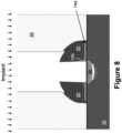
photoresist 26, which is patterned to remove the portion of the photoresist over thenitride block 16. Oxide, nitride and poly etches are performed to removeoxide layer 24 on thenitride block 16, thenitride block 16, and the portion of thepoly layer 14 exposed by the removal of thenitride block 16, leavingpoly blocks 14a having an upwardly sloping upper surface that terminates in asharp edge 14b. An implant process follows for forming thesource region 28 in thesubstrate 10 between theoxide spacers 20 andpoly blocks 14a (i.e., the source region is formed under a gap that exists between theoxide spacers 20 and a gap that exists between thepoly blocks 14a). The resulting structure is shown inFig. 8 . - A
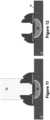
tunnel oxide layer 30 is then formed on the exposed ends of thepoly blocks 14a including thesharp edges 14b, as shown inFig. 9 . Specifically, thetunnel oxide layer 30 is formed by first performing an oxide etch (e.g., wet etch) to laterally recess the sidewall of eachspacer 20 away from the respective ends of thepoly blocks 14a, exposing thesharp edges 14b. Thetunnel oxide layer 30 is then formed by high temperature oxide HTO deposition. Thetunnel oxide layer 30 extends along the exposed sidewalls ofpoly layer blocks 14a, and wraps around thesharp edges 14b. However, the HTO deposition does not consume the polysiliconsharp edges 14b, thus maintaining their shape. - A wet oxidation is then used to thicken the
oxide 32 over thesource region 28 and thetunnel oxide layer 30 wrapping around thesharp edges 14b, as shown inFig. 10 . Photoresist 34 is then formed between theoxide spacers 20, and an oxide etch is used to remove the oxide layer on the substrate outside of the pair of spacers, leaving the substrate surface exposed, as shown inFig. 11 . Then, a thin oxide layer (WL oxide) 36 is formed on the substrate outside of the pair of spacers, as shown inFig. 12 (after photo resist removal). - A layer of
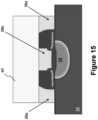
polysilicon 38 is then formed over the structure. This poly layer can be used in the logic areas of the same substrate. If it desirous for the poly layer thickness to be thicker in the memory array than the logic area, a cap oxide layer can be formed on thepoly layer 38 and patterned to remove the cap oxide layer from the memory area of the device, followed by the deposition of additional polysilicon to thicken thepoly layer 38 in the memory area. The additional polysilicon on the cap oxide layer in the logic area will later be removed by a poly CMP described below. The resulting structure is shown inFig. 13 . - The structure is then planarized by a poly CMP (chemical mechanical polish) to below the tops of the
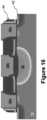
oxide spacers 20. Thepoly layer 38 can be doped by implantation with material and annealed at this time. The resulting structure is shown inFig. 14 . Photoresist 40 is formed on the structure and patterned leaving only those portions of thepoly layer 38 between theoxide spacers 20 and immediately outside of theoxide spacers 20 covered by the photo resist 40. A poly etch is then used to remove the exposed portions of thepoly layer 38 not protected by thephoto resist 40, leavingblocks 38a of thepoly layer 38 adjacent to the outsides of theoxide spacers 20, and ablock 38b of thepoly layer 38 between theoxide spacers 20. The resulting structure is shown inFig. 15 . - An implantation is then performed to form
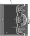
drain regions 42 in the substrate adjacent thepoly blocks 38a.Spacers 44 of insulation material are then formed on the outsides ofpoly blocks 38a. Preferably, these spacers are formed by forming one or more insulation layers (e.g., oxide, nitride, oxide) followed by one or more anisotropic etches, as shown inFig. 16 . An additional implant and anneal can then be used to further enhance thedrain regions 42. Salicide 46 is then formed on the exposed upper surfaces of the poly blocks 38a and 38b, for improved conductivity. ILD insulation is then formed over the structure, which preferably includesinsulation material 48a formed over insulation layers 48b. Contact holes are then formed through the ILD insulation, exposing thedrain regions 42. Conductive material is then formed on the structure and patterned, filling the contact holes, to form a bit line 50 extending over the ILD insulation 48, andcontacts 52 extending between and providing electrical conduction between the bit line 50 and thedrain regions 42. The final structure is shown inFig. 17 . - As shown in
Fig. 17 , the process forms pairs of memory cells. Each memory cell pair includes asource region 28 and twodrain regions 42, with two channel regions 54 each extending between thesource region 28 and one of thedrain regions 42. An erasegate 38b is disposed over and insulated from thesource region 28 by thethick oxide layer 32. Each memory cell includes a floatinggate 14a disposed over and insulated from a first portion of the channel region 54, and aword line gate 38a disposed over and insulated from a second portion of the channel region 54. The floatinggate 14a has asharp tip 14b (caused by the sloping surface) that faces a notch 56 formed in the erasegate 38b, whereby the erasegate 38b wraps around thesharp tip 14b of the floatinggate 14a. Thesharp tip 14b is insulated from the erasegate 38b by thetunnel oxide layer 30. Theword line gates 38a are insulated from the substrate by anoxide layer 36 that is thinner than theoxide 12 between the floatinggate 14a and thesubstrate 10, which is thinner than theoxide 32 between the erasegate 38b and thesource region 28. Theoxide layer 36 under theword line gate 38a and thetunnel oxide 30 are formed separately, and therefore can be separately adjusted in terms of thickness for optimal performance. - The cell size can be scaled down by shortening the portion of the channel region 54 under the
word line gate 38a (i.e., making the length ofword line gate 38a in the direction of the channel region shorter), and thinning theoxide layer 36 under theword line gate 38a (which can be done independently relative to other insulation layers such as the tunnel oxide that can remain thicker) which allows for a higher current drive for the memory cell. The erasegate 38b andword line gates 38a are formed by the same poly deposition, so only two poly depositions are needed to form the floatinggates 14a, theword line gates 38a and the erasegates 38b for all the memory cells. The length of eachword line gate 38a (in the direction of the channel region) is determined by photolithography for better dimension control. The height of theword line gates 38a and erasegate 38b are determine by chemical mechanical polish, which avoids defect issues that could exist should the word line gates instead be made by a poly spacer technique. The isolation (oxide) between the floatinggate 14a andword line gate 38a can be independently optimized, because that oxide is originally formed asoxide 22 which is then thickened by subsequent processing. Finally, thetunnel oxide 30 is formed as a single layer wrapping around the sharp tip of the floating gate, and thickened by a subsequent wet oxidation process. Using the above method, erase efficiency and word line gate performance can be independently optimized. - It is to be understood that the present invention is not limited to the embodiment(s) described above and illustrated herein, but encompasses any and all variations falling within the scope of any claims. Materials, processes and numerical examples described above are exemplary only, and should not be deemed to limit the claims. Further, not all method steps need be performed in the exact order illustrated or claimed, but rather in any order that allows the proper formation of the non-volatile memory cells of the present invention. Single layers of material could be formed as multiple layers of such or similar materials, and vice versa. Lastly, the terms "forming" and "formed" as used herein shall include material deposition, material growth, or any other technique in providing the material as disclosed or claimed.
- It should be noted that, as used herein, the terms "over" and "on" both inclusively include "directly on" (no intermediate materials, elements or space disposed there between) and "indirectly on" (intermediate materials, elements or space disposed there between). Likewise, the term "adjacent" includes "directly adjacent" (no intermediate materials, elements or space disposed there between) and "indirectly adjacent" (intermediate materials, elements or space disposed there between), "mounted to" includes "directly mounted to" (no intermediate materials, elements or space disposed there between) and "indirectly mounted to" (intermediate materials, elements or spaced disposed there between), and "electrically coupled" includes "directly electrically coupled to" (no intermediate materials or elements there between that electrically connect the elements together) and "indirectly electrically coupled to" (intermediate materials or elements there between that electrically connect the elements together). For example, forming an element "over a substrate" can include forming the element directly on the substrate with no intermediate materials/elements there between, as well as forming the element indirectly on the substrate with one or more intermediate materials/elements there between.
Claims (7)
- A method of forming a memory device, comprising:forming a first insulation layer (12) having a first thickness on a semiconductor substrate (10);forming a first polysilicon layer (14) on the first insulation layer;forming first and second spaced apart insulation spacers (20) directly on the first polysilicon layer;removing portions of the first polysilicon layer such that a first block of the first polysilicon layer (14a) remains under the first insulation spacer and a second block of the first polysilicon layer (14a) remains under the second insulation spacer, wherein each of the first and second blocks of the first polysilicon layer include opposing first and second side surfaces, the first side surfaces face toward each other and the second side surfaces face away from each other, and each of the first and second blocks of the first polysilicon layer has a sloping upper surface that terminates in a sharp edge (14b);forming oxide spacers (22) on the second side surfaces of the first and second blocks of the first polysilicon layer;thickening the oxide spacers;forming a source region (28) in the substrate that is disposed under a gap between the first and second blocks of the first polysilicon layer;forming a tunnel oxide layer (30) on the sharp edges and the first side surfaces of the first and second block of the first polysilicon layer;forming a second insulation layer (32) having a second thickness on the semiconductor substrate over the source region, wherein the forming of the second insulation layer includes thickening the tunnel oxide layer;forming a third insulation layer (36) having a third thickness directly on portions of the semiconductor substrate adjacent the second side surfaces of the first and second blocks of the first polysilicon layer;forming a second polysilicon layer (38) over the substrate and the first and second insulation spacers;removing portions of the second polysilicon layer using a chemical mechanical polish that also removes top portions of the insulation spacers such that a first block of the second polysilicon layer (38b) remains that is disposed on the second insulation layer and between the first and second insulation spacers, and second and third blocks of the second polysilicon layer (38a) remain that are disposed on the third insulation layer such that the second and third blocks of the second polysilicon layer are insulated from the substrate only by the third insulation layer, wherein the first insulation spacer is disposed between the first and second blocks of the second polysilicon layer and wherein the second insulation spacer is disposed between the first and third blocks of the second polysilicon layer;forming a first drain region (42) in the substrate adjacent the second block of the second polysilicon layer; andforming a second drain region (42) in the substrate adjacent the third block of the second polysilicon layer;wherein the first block of the second polysilicon layer includes a first notch (56) that wraps around and is insulated from the sharp edge of the first block of the first polysilicon layer and a second notch (56) that wraps around and is insulated from the sharp edge of the second block of the first polysilicon layer;wherein the second thickness is greater than the first thickness, and wherein the first thickness is greater than the third thickness.
- The method of claim 1, further comprising:
forming salicide (46) on upper surfaces of the first, second and third blocks of the second polysilicon layer. - The method of claim 1, wherein the forming of the first and second insulation spacers includes:forming a block of nitride (16) on the first polysilicon layer;forming oxide on the block of nitride and on the first polysilicon layer;performing an oxide etch to remove portions of the oxide except for the first and second insulation spacers of the oxide abutting side surfaces of the block of nitride; andremoving the block of nitride.
- The method of claim 1, wherein the sloping upper surfaces of the first and second blocks of the first polysilicon layer are formed by:forming a block of nitride (16) on the first polysilicon layer;performing a poly etch on the upper surface of the first polysilicon layer so that the upper surface of the first polysilicon layer slopes upwardly as it approaches sidewalls of the block of nitride.
- The method of claim 1, wherein the removing of the portions of the second polysilicon layer includes a photolithographic etch of the second polysilicon layer.
- The method of claim 1, wherein:the first insulation layer is oxide;the second insulation layer is oxide; andthe third insulation layer is oxide.
- The method of claim 1, wherein:the first and second notches of the first block of the second polysilicon layer are insulated from the first and second blocks of the first polysilicon layer, respectively, by the tunnel oxide layer having a fourth thickness; andthe third thickness is less than the fourth thickness.
Applications Claiming Priority (3)
| Application Number | Priority Date | Filing Date | Title |
|---|---|---|---|
| US201862669263P | 2018-05-09 | 2018-05-09 | |
| US16/057,750US10418451B1 (en) | 2018-05-09 | 2018-08-07 | Split-gate flash memory cell with varying insulation gate oxides, and method of forming same |
| PCT/US2019/026671WO2019217022A1 (en) | 2018-05-09 | 2019-04-09 | Split-gate flash memory cell with varying insulation gate oxides, and method of forming same |
Publications (3)
| Publication Number | Publication Date |
|---|---|
| EP3815149A1 EP3815149A1 (en) | 2021-05-05 |
| EP3815149A4 EP3815149A4 (en) | 2022-06-15 |
| EP3815149B1true EP3815149B1 (en) | 2023-08-09 |
Family
ID=67909170
Family Applications (1)
| Application Number | Title | Priority Date | Filing Date |
|---|---|---|---|
| EP19799678.8AActiveEP3815149B1 (en) | 2018-05-09 | 2019-04-09 | Split-gate flash memory cell with varying insulation gate oxides, and method of forming same |
Country Status (7)
| Country | Link |
|---|---|
| US (1) | US10418451B1 (en) |
| EP (1) | EP3815149B1 (en) |
| JP (1) | JP7316302B2 (en) |
| KR (1) | KR102397576B1 (en) |
| CN (1) | CN112074958B (en) |
| TW (1) | TWI681543B (en) |
| WO (1) | WO2019217022A1 (en) |
Families Citing this family (8)
| Publication number | Priority date | Publication date | Assignee | Title |
|---|---|---|---|---|
| CN112185970B (en) | 2019-07-02 | 2024-05-28 | 硅存储技术公司 | Method of forming a split gate memory cell |
| CN112185815B (en) | 2019-07-04 | 2024-07-23 | 硅存储技术公司 | Method for forming split gate flash memory cell |
| US11018147B1 (en)* | 2020-02-04 | 2021-05-25 | Silicon Storage Technology, Inc. | Method of forming split gate memory cells with thinned tunnel oxide |
| US11362218B2 (en)* | 2020-06-23 | 2022-06-14 | Silicon Storage Technology, Inc. | Method of forming split gate memory cells with thinned side edge tunnel oxide |
| CN114335186B (en)* | 2020-09-30 | 2025-02-07 | 硅存储技术股份有限公司 | Split gate non-volatile memory cell with erase gate disposed above word line gate and method of making the same |
| CN115083912B (en)* | 2021-03-11 | 2025-05-27 | 硅存储技术股份有限公司 | Split-gate memory cell with improved control gate capacitive coupling and method of manufacturing the same |
| US11462622B1 (en)* | 2021-06-23 | 2022-10-04 | Globalfoundries Singapore Pte. Ltd. | Memory cells and methods of forming a memory cell |
| TW202329418A (en) | 2022-01-11 | 2023-07-16 | 聯華電子股份有限公司 | Smeiconductor memory device |
Family Cites Families (24)
| Publication number | Priority date | Publication date | Assignee | Title |
|---|---|---|---|---|
| US5029130A (en) | 1990-01-22 | 1991-07-02 | Silicon Storage Technology, Inc. | Single transistor non-valatile electrically alterable semiconductor memory device |
| US5856943A (en)* | 1996-03-18 | 1999-01-05 | Integrated Memory Technologies, Inc. | Scalable flash EEPROM memory cell and array |
| JP4222675B2 (en) | 1999-03-29 | 2009-02-12 | 三洋電機株式会社 | Nonvolatile semiconductor memory device |
| US6727545B2 (en) | 2000-09-20 | 2004-04-27 | Silicon Storage Technology, Inc. | Semiconductor memory array of floating gate memory cells with low resistance source regions and high source coupling |
| US6952034B2 (en) | 2002-04-05 | 2005-10-04 | Silicon Storage Technology, Inc. | Semiconductor memory array of floating gate memory cells with buried source line and floating gate |
| US6747310B2 (en) | 2002-10-07 | 2004-06-08 | Actrans System Inc. | Flash memory cells with separated self-aligned select and erase gates, and process of fabrication |
| US7315056B2 (en) | 2004-06-07 | 2008-01-01 | Silicon Storage Technology, Inc. | Semiconductor memory array of floating gate memory cells with program/erase and select gates |
| TWI284415B (en)* | 2005-10-26 | 2007-07-21 | Promos Technologies Inc | Split gate flash memory cell and fabrication method thereof |
| US20090039410A1 (en) | 2007-08-06 | 2009-02-12 | Xian Liu | Split Gate Non-Volatile Flash Memory Cell Having A Floating Gate, Control Gate, Select Gate And An Erase Gate With An Overhang Over The Floating Gate, Array And Method Of Manufacturing |
| CN102956643A (en)* | 2011-08-24 | 2013-03-06 | 硅存储技术公司 | Non-volatile floating gate storage unit manufacturing method and storage unit manufactured by same |
| US8878281B2 (en) | 2012-05-23 | 2014-11-04 | Taiwan Semiconductor Manufacturing Company, Ltd. | Methods and apparatus for non-volatile memory cells |
| US9018690B2 (en) | 2012-09-28 | 2015-04-28 | Silicon Storage Technology, Inc. | Split-gate memory cell with substrate stressor region, and method of making same |
| JP2015130438A (en)* | 2014-01-08 | 2015-07-16 | ルネサスエレクトロニクス株式会社 | Semiconductor device and semiconductor device manufacturing method |
| US20150213898A1 (en) | 2014-01-27 | 2015-07-30 | Silicon Storage Technololgy, Inc. | Byte Erasable Non-volatile Memory Architecture And Method Of Erasing Same |
| US20150255614A1 (en)* | 2014-03-05 | 2015-09-10 | Powerchip Technology Corporation | Split gate flash memory and manufacturing method thereof |
| KR102240022B1 (en)* | 2014-11-26 | 2021-04-15 | 삼성전자주식회사 | Semicondcutor device and manufacturing method for the same |
| CN105990367B (en)* | 2015-02-27 | 2019-03-12 | 硅存储技术公司 | Nonvolatile memory cell array with ROM cells |
| US9917165B2 (en)* | 2015-05-15 | 2018-03-13 | Taiwan Semiconductor Manufacturing Co., Ltd. | Memory cell structure for improving erase speed |
| US9793279B2 (en)* | 2015-07-10 | 2017-10-17 | Silicon Storage Technology, Inc. | Split gate non-volatile memory cell having a floating gate, word line, erase gate, and method of manufacturing |
| US9793281B2 (en)* | 2015-07-21 | 2017-10-17 | Silicon Storage Technology, Inc. | Non-volatile split gate memory cells with integrated high K metal gate logic device and metal-free erase gate, and method of making same |
| US9859291B2 (en) | 2015-08-03 | 2018-01-02 | Iotmemory Technology Inc. | Non-volatile memory and manufacturing method thereof |
| US10141321B2 (en)* | 2015-10-21 | 2018-11-27 | Silicon Storage Technology, Inc. | Method of forming flash memory with separate wordline and erase gates |
| EP3371829B1 (en)* | 2015-11-03 | 2020-11-25 | Silicon Storage Technology, Inc. | Integration of split gate non-volatile flash memory with finfet logic |
| WO2017184315A1 (en) | 2016-04-20 | 2017-10-26 | Silicon Storage Technology, Inc. | Method of forming pairs of three-gate non-volatile flash memory cells using two polysilicon deposition steps |
- 2018
- 2018-08-07USUS16/057,750patent/US10418451B1/enactiveActive
- 2019
- 2019-04-09WOPCT/US2019/026671patent/WO2019217022A1/ennot_activeCeased
- 2019-04-09EPEP19799678.8Apatent/EP3815149B1/enactiveActive
- 2019-04-09CNCN201980030337.8Apatent/CN112074958B/enactiveActive
- 2019-04-09JPJP2020562590Apatent/JP7316302B2/enactiveActive
- 2019-04-09KRKR1020207031428Apatent/KR102397576B1/enactiveActive
- 2019-05-03TWTW108115433Apatent/TWI681543B/enactive
Also Published As
| Publication number | Publication date |
|---|---|
| TWI681543B (en) | 2020-01-01 |
| EP3815149A1 (en) | 2021-05-05 |
| JP7316302B2 (en) | 2023-07-27 |
| KR20200140312A (en) | 2020-12-15 |
| KR102397576B1 (en) | 2022-05-12 |
| CN112074958B (en) | 2024-09-03 |
| TW201947741A (en) | 2019-12-16 |
| EP3815149A4 (en) | 2022-06-15 |
| WO2019217022A1 (en) | 2019-11-14 |
| JP2021523566A (en) | 2021-09-02 |
| CN112074958A (en) | 2020-12-11 |
| US10418451B1 (en) | 2019-09-17 |
Similar Documents
| Publication | Publication Date | Title |
|---|---|---|
| EP3815149B1 (en) | Split-gate flash memory cell with varying insulation gate oxides, and method of forming same | |
| CN111418063B (en) | Non-volatile split-gate memory cell with integrated high-K metal control gate and method of fabrication | |
| CN107112328B (en) | Nonvolatile memory array with simultaneously formed low voltage logic devices and high voltage logic devices | |
| US11652162B2 (en) | Method of forming a three-gate non-volatile flash memory cell using two polysilicon deposition steps | |
| TWI590313B (en) | Method of forming a self-aligned separation gate memory cell array including metal gates and logic devices | |
| TW202005061A (en) | Split gate non-volatile memory cells and logic devices with FINFET structure, and method of making same | |
| CN111133515B (en) | Method of fabricating a split gate flash memory cell with erase gate | |
| KR20170039297A (en) | Split-gate flash memory cell with improved scaling using enhanced lateral control gate to floating gate coupling | |
| TWI752727B (en) | Method of forming a device with split gate non-volatile memory cells, hv devices having planar channel regions and finfet logic devices | |
| KR102763644B1 (en) | Split gate, 2-bit nonvolatile memory cell having an erase gate arranged over a word line gate, and method for manufacturing the same | |
| KR20180132950A (en) | Detachable-gate, twin-bit non-volatile memory cells | |
| CN112185970A (en) | Method of forming split gate memory cell | |
| CN112400230A (en) | Split-gate non-volatile memory cell with three-dimensional fin field effect transistor structure and manufacturing method thereof | |
| EP3994731B1 (en) | Method of forming split-gate flash memory cell with spacer defined floating gate and discretely formed polysilicon gates | |
| CN109699188B (en) | Method of forming a low-height split-gate memory cell | |
| WO2017184315A1 (en) | Method of forming pairs of three-gate non-volatile flash memory cells using two polysilicon deposition steps | |
| JP7522869B2 (en) | Method for forming a split-gate memory cell having a thinned side edge tunnel oxide - Patents.com |
Legal Events
| Date | Code | Title | Description |
|---|---|---|---|
| STAA | Information on the status of an ep patent application or granted ep patent | Free format text:STATUS: THE INTERNATIONAL PUBLICATION HAS BEEN MADE | |
| PUAI | Public reference made under article 153(3) epc to a published international application that has entered the european phase | Free format text:ORIGINAL CODE: 0009012 | |
| STAA | Information on the status of an ep patent application or granted ep patent | Free format text:STATUS: REQUEST FOR EXAMINATION WAS MADE | |
| 17P | Request for examination filed | Effective date:20201203 | |
| AK | Designated contracting states | Kind code of ref document:A1 Designated state(s):AL AT BE BG CH CY CZ DE DK EE ES FI FR GB GR HR HU IE IS IT LI LT LU LV MC MK MT NL NO PL PT RO RS SE SI SK SM TR | |
| DAV | Request for validation of the european patent (deleted) | ||
| DAX | Request for extension of the european patent (deleted) | ||
| RIC1 | Information provided on ipc code assigned before grant | Ipc:H01L 27/11521 20170101ALI20220114BHEP Ipc:H01L 29/423 20060101AFI20220114BHEP | |
| A4 | Supplementary search report drawn up and despatched | Effective date:20220513 | |
| RIC1 | Information provided on ipc code assigned before grant | Ipc:H01L 27/11521 20170101ALI20220509BHEP Ipc:H01L 29/423 20060101AFI20220509BHEP | |
| REG | Reference to a national code | Ref country code:DE Ref legal event code:R079 Free format text:PREVIOUS MAIN CLASS: H01L0029660000 Ipc:H01L0029423000 Ref document number:602019034721 Country of ref document:DE | |
| GRAP | Despatch of communication of intention to grant a patent | Free format text:ORIGINAL CODE: EPIDOSNIGR1 | |
| STAA | Information on the status of an ep patent application or granted ep patent | Free format text:STATUS: GRANT OF PATENT IS INTENDED | |
| RIC1 | Information provided on ipc code assigned before grant | Ipc:H10B 41/30 20230101ALI20230210BHEP Ipc:H01L 29/423 20060101AFI20230210BHEP | |
| INTG | Intention to grant announced | Effective date:20230307 | |
| P01 | Opt-out of the competence of the unified patent court (upc) registered | Effective date:20230519 | |
| GRAS | Grant fee paid | Free format text:ORIGINAL CODE: EPIDOSNIGR3 | |
| GRAA | (expected) grant | Free format text:ORIGINAL CODE: 0009210 | |
| STAA | Information on the status of an ep patent application or granted ep patent | Free format text:STATUS: THE PATENT HAS BEEN GRANTED | |
| AK | Designated contracting states | Kind code of ref document:B1 Designated state(s):AL AT BE BG CH CY CZ DE DK EE ES FI FR GB GR HR HU IE IS IT LI LT LU LV MC MK MT NL NO PL PT RO RS SE SI SK SM TR | |
| REG | Reference to a national code | Ref country code:GB Ref legal event code:FG4D | |
| REG | Reference to a national code | Ref country code:CH Ref legal event code:EP | |
| REG | Reference to a national code | Ref country code:IE Ref legal event code:FG4D | |
| REG | Reference to a national code | Ref country code:DE Ref legal event code:R096 Ref document number:602019034721 Country of ref document:DE | |
| REG | Reference to a national code | Ref country code:NL Ref legal event code:FP | |
| REG | Reference to a national code | Ref country code:LT Ref legal event code:MG9D | |
| REG | Reference to a national code | Ref country code:AT Ref legal event code:MK05 Ref document number:1598535 Country of ref document:AT Kind code of ref document:T Effective date:20230809 | |
| PG25 | Lapsed in a contracting state [announced via postgrant information from national office to epo] | Ref country code:GR Free format text:LAPSE BECAUSE OF FAILURE TO SUBMIT A TRANSLATION OF THE DESCRIPTION OR TO PAY THE FEE WITHIN THE PRESCRIBED TIME-LIMIT Effective date:20231110 | |
| PG25 | Lapsed in a contracting state [announced via postgrant information from national office to epo] | Ref country code:IS Free format text:LAPSE BECAUSE OF FAILURE TO SUBMIT A TRANSLATION OF THE DESCRIPTION OR TO PAY THE FEE WITHIN THE PRESCRIBED TIME-LIMIT Effective date:20231209 | |
| PG25 | Lapsed in a contracting state [announced via postgrant information from national office to epo] | Ref country code:SE Free format text:LAPSE BECAUSE OF FAILURE TO SUBMIT A TRANSLATION OF THE DESCRIPTION OR TO PAY THE FEE WITHIN THE PRESCRIBED TIME-LIMIT Effective date:20230809 Ref country code:RS Free format text:LAPSE BECAUSE OF FAILURE TO SUBMIT A TRANSLATION OF THE DESCRIPTION OR TO PAY THE FEE WITHIN THE PRESCRIBED TIME-LIMIT Effective date:20230809 Ref country code:PT Free format text:LAPSE BECAUSE OF FAILURE TO SUBMIT A TRANSLATION OF THE DESCRIPTION OR TO PAY THE FEE WITHIN THE PRESCRIBED TIME-LIMIT Effective date:20231211 Ref country code:NO Free format text:LAPSE BECAUSE OF FAILURE TO SUBMIT A TRANSLATION OF THE DESCRIPTION OR TO PAY THE FEE WITHIN THE PRESCRIBED TIME-LIMIT Effective date:20231109 Ref country code:LV Free format text:LAPSE BECAUSE OF FAILURE TO SUBMIT A TRANSLATION OF THE DESCRIPTION OR TO PAY THE FEE WITHIN THE PRESCRIBED TIME-LIMIT Effective date:20230809 Ref country code:LT Free format text:LAPSE BECAUSE OF FAILURE TO SUBMIT A TRANSLATION OF THE DESCRIPTION OR TO PAY THE FEE WITHIN THE PRESCRIBED TIME-LIMIT Effective date:20230809 Ref country code:IS Free format text:LAPSE BECAUSE OF FAILURE TO SUBMIT A TRANSLATION OF THE DESCRIPTION OR TO PAY THE FEE WITHIN THE PRESCRIBED TIME-LIMIT Effective date:20231209 Ref country code:HR Free format text:LAPSE BECAUSE OF FAILURE TO SUBMIT A TRANSLATION OF THE DESCRIPTION OR TO PAY THE FEE WITHIN THE PRESCRIBED TIME-LIMIT Effective date:20230809 Ref country code:GR Free format text:LAPSE BECAUSE OF FAILURE TO SUBMIT A TRANSLATION OF THE DESCRIPTION OR TO PAY THE FEE WITHIN THE PRESCRIBED TIME-LIMIT Effective date:20231110 Ref country code:FI Free format text:LAPSE BECAUSE OF FAILURE TO SUBMIT A TRANSLATION OF THE DESCRIPTION OR TO PAY THE FEE WITHIN THE PRESCRIBED TIME-LIMIT Effective date:20230809 Ref country code:AT Free format text:LAPSE BECAUSE OF FAILURE TO SUBMIT A TRANSLATION OF THE DESCRIPTION OR TO PAY THE FEE WITHIN THE PRESCRIBED TIME-LIMIT Effective date:20230809 | |
| PG25 | Lapsed in a contracting state [announced via postgrant information from national office to epo] | Ref country code:PL Free format text:LAPSE BECAUSE OF FAILURE TO SUBMIT A TRANSLATION OF THE DESCRIPTION OR TO PAY THE FEE WITHIN THE PRESCRIBED TIME-LIMIT Effective date:20230809 | |
| PG25 | Lapsed in a contracting state [announced via postgrant information from national office to epo] | Ref country code:ES Free format text:LAPSE BECAUSE OF FAILURE TO SUBMIT A TRANSLATION OF THE DESCRIPTION OR TO PAY THE FEE WITHIN THE PRESCRIBED TIME-LIMIT Effective date:20230809 | |
| PG25 | Lapsed in a contracting state [announced via postgrant information from national office to epo] | Ref country code:SM Free format text:LAPSE BECAUSE OF FAILURE TO SUBMIT A TRANSLATION OF THE DESCRIPTION OR TO PAY THE FEE WITHIN THE PRESCRIBED TIME-LIMIT Effective date:20230809 Ref country code:RO Free format text:LAPSE BECAUSE OF FAILURE TO SUBMIT A TRANSLATION OF THE DESCRIPTION OR TO PAY THE FEE WITHIN THE PRESCRIBED TIME-LIMIT Effective date:20230809 Ref country code:ES Free format text:LAPSE BECAUSE OF FAILURE TO SUBMIT A TRANSLATION OF THE DESCRIPTION OR TO PAY THE FEE WITHIN THE PRESCRIBED TIME-LIMIT Effective date:20230809 Ref country code:EE Free format text:LAPSE BECAUSE OF FAILURE TO SUBMIT A TRANSLATION OF THE DESCRIPTION OR TO PAY THE FEE WITHIN THE PRESCRIBED TIME-LIMIT Effective date:20230809 Ref country code:DK Free format text:LAPSE BECAUSE OF FAILURE TO SUBMIT A TRANSLATION OF THE DESCRIPTION OR TO PAY THE FEE WITHIN THE PRESCRIBED TIME-LIMIT Effective date:20230809 Ref country code:CZ Free format text:LAPSE BECAUSE OF FAILURE TO SUBMIT A TRANSLATION OF THE DESCRIPTION OR TO PAY THE FEE WITHIN THE PRESCRIBED TIME-LIMIT Effective date:20230809 Ref country code:SK Free format text:LAPSE BECAUSE OF FAILURE TO SUBMIT A TRANSLATION OF THE DESCRIPTION OR TO PAY THE FEE WITHIN THE PRESCRIBED TIME-LIMIT Effective date:20230809 | |
| REG | Reference to a national code | Ref country code:DE Ref legal event code:R097 Ref document number:602019034721 Country of ref document:DE | |
| PG25 | Lapsed in a contracting state [announced via postgrant information from national office to epo] | Ref country code:IT Free format text:LAPSE BECAUSE OF FAILURE TO SUBMIT A TRANSLATION OF THE DESCRIPTION OR TO PAY THE FEE WITHIN THE PRESCRIBED TIME-LIMIT Effective date:20230809 | |
| PLBE | No opposition filed within time limit | Free format text:ORIGINAL CODE: 0009261 | |
| STAA | Information on the status of an ep patent application or granted ep patent | Free format text:STATUS: NO OPPOSITION FILED WITHIN TIME LIMIT | |
| 26N | No opposition filed | Effective date:20240513 | |
| PG25 | Lapsed in a contracting state [announced via postgrant information from national office to epo] | Ref country code:SI Free format text:LAPSE BECAUSE OF FAILURE TO SUBMIT A TRANSLATION OF THE DESCRIPTION OR TO PAY THE FEE WITHIN THE PRESCRIBED TIME-LIMIT Effective date:20230809 | |
| PG25 | Lapsed in a contracting state [announced via postgrant information from national office to epo] | Ref country code:BG Free format text:LAPSE BECAUSE OF FAILURE TO SUBMIT A TRANSLATION OF THE DESCRIPTION OR TO PAY THE FEE WITHIN THE PRESCRIBED TIME-LIMIT Effective date:20230809 | |
| PG25 | Lapsed in a contracting state [announced via postgrant information from national office to epo] | Ref country code:MC Free format text:LAPSE BECAUSE OF FAILURE TO SUBMIT A TRANSLATION OF THE DESCRIPTION OR TO PAY THE FEE WITHIN THE PRESCRIBED TIME-LIMIT Effective date:20230809 | |
| REG | Reference to a national code | Ref country code:DE Ref legal event code:R079 Ref document number:602019034721 Country of ref document:DE Free format text:PREVIOUS MAIN CLASS: H01L0029423000 Ipc:H10D0064270000 | |
| PG25 | Lapsed in a contracting state [announced via postgrant information from national office to epo] | Ref country code:MC Free format text:LAPSE BECAUSE OF FAILURE TO SUBMIT A TRANSLATION OF THE DESCRIPTION OR TO PAY THE FEE WITHIN THE PRESCRIBED TIME-LIMIT Effective date:20230809 Ref country code:BG Free format text:LAPSE BECAUSE OF FAILURE TO SUBMIT A TRANSLATION OF THE DESCRIPTION OR TO PAY THE FEE WITHIN THE PRESCRIBED TIME-LIMIT Effective date:20230809 | |
| REG | Reference to a national code | Ref country code:CH Ref legal event code:PL | |
| PG25 | Lapsed in a contracting state [announced via postgrant information from national office to epo] | Ref country code:LU Free format text:LAPSE BECAUSE OF NON-PAYMENT OF DUE FEES Effective date:20240409 | |
| GBPC | Gb: european patent ceased through non-payment of renewal fee | Effective date:20240409 | |
| REG | Reference to a national code | Ref country code:BE Ref legal event code:MM Effective date:20240430 | |
| PG25 | Lapsed in a contracting state [announced via postgrant information from national office to epo] | Ref country code:LU Free format text:LAPSE BECAUSE OF NON-PAYMENT OF DUE FEES Effective date:20240409 | |
| PG25 | Lapsed in a contracting state [announced via postgrant information from national office to epo] | Ref country code:BE Free format text:LAPSE BECAUSE OF NON-PAYMENT OF DUE FEES Effective date:20240430 | |
| PG25 | Lapsed in a contracting state [announced via postgrant information from national office to epo] | Ref country code:GB Free format text:LAPSE BECAUSE OF NON-PAYMENT OF DUE FEES Effective date:20240409 | |
| PG25 | Lapsed in a contracting state [announced via postgrant information from national office to epo] | Ref country code:GB Free format text:LAPSE BECAUSE OF NON-PAYMENT OF DUE FEES Effective date:20240409 Ref country code:BE Free format text:LAPSE BECAUSE OF NON-PAYMENT OF DUE FEES Effective date:20240430 Ref country code:CH Free format text:LAPSE BECAUSE OF NON-PAYMENT OF DUE FEES Effective date:20240430 | |
| PGFP | Annual fee paid to national office [announced via postgrant information from national office to epo] | Ref country code:NL Payment date:20250319 Year of fee payment:7 | |
| PG25 | Lapsed in a contracting state [announced via postgrant information from national office to epo] | Ref country code:IE Free format text:LAPSE BECAUSE OF NON-PAYMENT OF DUE FEES Effective date:20240409 | |
| PGFP | Annual fee paid to national office [announced via postgrant information from national office to epo] | Ref country code:FR Payment date:20250319 Year of fee payment:7 | |
| PGFP | Annual fee paid to national office [announced via postgrant information from national office to epo] | Ref country code:DE Payment date:20250319 Year of fee payment:7 | |
| PG25 | Lapsed in a contracting state [announced via postgrant information from national office to epo] | Ref country code:CY Free format text:LAPSE BECAUSE OF FAILURE TO SUBMIT A TRANSLATION OF THE DESCRIPTION OR TO PAY THE FEE WITHIN THE PRESCRIBED TIME-LIMIT; INVALID AB INITIO Effective date:20190409 | |
| PG25 | Lapsed in a contracting state [announced via postgrant information from national office to epo] | Ref country code:HU Free format text:LAPSE BECAUSE OF FAILURE TO SUBMIT A TRANSLATION OF THE DESCRIPTION OR TO PAY THE FEE WITHIN THE PRESCRIBED TIME-LIMIT; INVALID AB INITIO Effective date:20190409 |